EP3770928A1 - Coupled output inductor and system - Google Patents
Coupled output inductor and system Download PDFInfo
- Publication number
- EP3770928A1 EP3770928A1 EP20187494.8A EP20187494A EP3770928A1 EP 3770928 A1 EP3770928 A1 EP 3770928A1 EP 20187494 A EP20187494 A EP 20187494A EP 3770928 A1 EP3770928 A1 EP 3770928A1
- Authority
- EP
- European Patent Office
- Prior art keywords
- output inductor
- ferromagnetic
- coupled output
- core
- shielding
- Prior art date
- Legal status (The legal status is an assumption and is not a legal conclusion. Google has not performed a legal analysis and makes no representation as to the accuracy of the status listed.)
- Granted
Links
Images


Classifications
-
- H—ELECTRICITY
- H01—ELECTRIC ELEMENTS
- H01F—MAGNETS; INDUCTANCES; TRANSFORMERS; SELECTION OF MATERIALS FOR THEIR MAGNETIC PROPERTIES
- H01F3/00—Cores, Yokes, or armatures
- H01F3/10—Composite arrangements of magnetic circuits
-
- H—ELECTRICITY
- H01—ELECTRIC ELEMENTS
- H01F—MAGNETS; INDUCTANCES; TRANSFORMERS; SELECTION OF MATERIALS FOR THEIR MAGNETIC PROPERTIES
- H01F17/00—Fixed inductances of the signal type
- H01F17/04—Fixed inductances of the signal type with magnetic core
- H01F17/06—Fixed inductances of the signal type with magnetic core with core substantially closed in itself, e.g. toroid
-
- H—ELECTRICITY
- H01—ELECTRIC ELEMENTS
- H01F—MAGNETS; INDUCTANCES; TRANSFORMERS; SELECTION OF MATERIALS FOR THEIR MAGNETIC PROPERTIES
- H01F27/00—Details of transformers or inductances, in general
- H01F27/24—Magnetic cores
- H01F27/26—Fastening parts of the core together; Fastening or mounting the core on casing or support
-
- H—ELECTRICITY
- H01—ELECTRIC ELEMENTS
- H01F—MAGNETS; INDUCTANCES; TRANSFORMERS; SELECTION OF MATERIALS FOR THEIR MAGNETIC PROPERTIES
- H01F27/00—Details of transformers or inductances, in general
- H01F27/34—Special means for preventing or reducing unwanted electric or magnetic effects, e.g. no-load losses, reactive currents, harmonics, oscillations, leakage fields
- H01F27/346—Preventing or reducing leakage fields
-
- H—ELECTRICITY
- H01—ELECTRIC ELEMENTS
- H01F—MAGNETS; INDUCTANCES; TRANSFORMERS; SELECTION OF MATERIALS FOR THEIR MAGNETIC PROPERTIES
- H01F27/00—Details of transformers or inductances, in general
- H01F27/34—Special means for preventing or reducing unwanted electric or magnetic effects, e.g. no-load losses, reactive currents, harmonics, oscillations, leakage fields
- H01F27/36—Electric or magnetic shields or screens
-
- H—ELECTRICITY
- H01—ELECTRIC ELEMENTS
- H01F—MAGNETS; INDUCTANCES; TRANSFORMERS; SELECTION OF MATERIALS FOR THEIR MAGNETIC PROPERTIES
- H01F3/00—Cores, Yokes, or armatures
- H01F3/10—Composite arrangements of magnetic circuits
- H01F3/14—Constrictions; Gaps, e.g. air-gaps
-
- H—ELECTRICITY
- H01—ELECTRIC ELEMENTS
- H01F—MAGNETS; INDUCTANCES; TRANSFORMERS; SELECTION OF MATERIALS FOR THEIR MAGNETIC PROPERTIES
- H01F37/00—Fixed inductances not covered by group H01F17/00
-
- H—ELECTRICITY
- H02—GENERATION; CONVERSION OR DISTRIBUTION OF ELECTRIC POWER
- H02M—APPARATUS FOR CONVERSION BETWEEN AC AND AC, BETWEEN AC AND DC, OR BETWEEN DC AND DC, AND FOR USE WITH MAINS OR SIMILAR POWER SUPPLY SYSTEMS; CONVERSION OF DC OR AC INPUT POWER INTO SURGE OUTPUT POWER; CONTROL OR REGULATION THEREOF
- H02M1/00—Details of apparatus for conversion
- H02M1/44—Circuits or arrangements for compensating for electromagnetic interference in converters or inverters
-
- H—ELECTRICITY
- H02—GENERATION; CONVERSION OR DISTRIBUTION OF ELECTRIC POWER
- H02M—APPARATUS FOR CONVERSION BETWEEN AC AND AC, BETWEEN AC AND DC, OR BETWEEN DC AND DC, AND FOR USE WITH MAINS OR SIMILAR POWER SUPPLY SYSTEMS; CONVERSION OF DC OR AC INPUT POWER INTO SURGE OUTPUT POWER; CONTROL OR REGULATION THEREOF
- H02M3/00—Conversion of DC power input into DC power output
- H02M3/02—Conversion of DC power input into DC power output without intermediate conversion into AC
- H02M3/04—Conversion of DC power input into DC power output without intermediate conversion into AC by static converters
- H02M3/10—Conversion of DC power input into DC power output without intermediate conversion into AC by static converters using discharge tubes with control electrode or semiconductor devices with control electrode
- H02M3/145—Conversion of DC power input into DC power output without intermediate conversion into AC by static converters using discharge tubes with control electrode or semiconductor devices with control electrode using devices of a triode or transistor type requiring continuous application of a control signal
- H02M3/155—Conversion of DC power input into DC power output without intermediate conversion into AC by static converters using discharge tubes with control electrode or semiconductor devices with control electrode using devices of a triode or transistor type requiring continuous application of a control signal using semiconductor devices only
- H02M3/156—Conversion of DC power input into DC power output without intermediate conversion into AC by static converters using discharge tubes with control electrode or semiconductor devices with control electrode using devices of a triode or transistor type requiring continuous application of a control signal using semiconductor devices only with automatic control of output voltage or current, e.g. switching regulators
- H02M3/158—Conversion of DC power input into DC power output without intermediate conversion into AC by static converters using discharge tubes with control electrode or semiconductor devices with control electrode using devices of a triode or transistor type requiring continuous application of a control signal using semiconductor devices only with automatic control of output voltage or current, e.g. switching regulators including plural semiconductor devices as final control devices for a single load
- H02M3/1584—Conversion of DC power input into DC power output without intermediate conversion into AC by static converters using discharge tubes with control electrode or semiconductor devices with control electrode using devices of a triode or transistor type requiring continuous application of a control signal using semiconductor devices only with automatic control of output voltage or current, e.g. switching regulators including plural semiconductor devices as final control devices for a single load with a plurality of power processing stages connected in parallel
-
- H—ELECTRICITY
- H02—GENERATION; CONVERSION OR DISTRIBUTION OF ELECTRIC POWER
- H02M—APPARATUS FOR CONVERSION BETWEEN AC AND AC, BETWEEN AC AND DC, OR BETWEEN DC AND DC, AND FOR USE WITH MAINS OR SIMILAR POWER SUPPLY SYSTEMS; CONVERSION OF DC OR AC INPUT POWER INTO SURGE OUTPUT POWER; CONTROL OR REGULATION THEREOF
- H02M3/00—Conversion of DC power input into DC power output
- H02M3/22—Conversion of DC power input into DC power output with intermediate conversion into AC
- H02M3/24—Conversion of DC power input into DC power output with intermediate conversion into AC by static converters
- H02M3/28—Conversion of DC power input into DC power output with intermediate conversion into AC by static converters using discharge tubes with control electrode or semiconductor devices with control electrode to produce the intermediate AC
- H02M3/325—Conversion of DC power input into DC power output with intermediate conversion into AC by static converters using discharge tubes with control electrode or semiconductor devices with control electrode to produce the intermediate AC using devices of a triode or a transistor type requiring continuous application of a control signal
- H02M3/335—Conversion of DC power input into DC power output with intermediate conversion into AC by static converters using discharge tubes with control electrode or semiconductor devices with control electrode to produce the intermediate AC using devices of a triode or a transistor type requiring continuous application of a control signal using semiconductor devices only
- H02M3/337—Conversion of DC power input into DC power output with intermediate conversion into AC by static converters using discharge tubes with control electrode or semiconductor devices with control electrode to produce the intermediate AC using devices of a triode or a transistor type requiring continuous application of a control signal using semiconductor devices only in push-pull configuration
-
- H—ELECTRICITY
- H01—ELECTRIC ELEMENTS
- H01F—MAGNETS; INDUCTANCES; TRANSFORMERS; SELECTION OF MATERIALS FOR THEIR MAGNETIC PROPERTIES
- H01F27/00—Details of transformers or inductances, in general
- H01F27/34—Special means for preventing or reducing unwanted electric or magnetic effects, e.g. no-load losses, reactive currents, harmonics, oscillations, leakage fields
- H01F27/36—Electric or magnetic shields or screens
- H01F27/366—Electric or magnetic shields or screens made of ferromagnetic material
-
- H—ELECTRICITY
- H01—ELECTRIC ELEMENTS
- H01F—MAGNETS; INDUCTANCES; TRANSFORMERS; SELECTION OF MATERIALS FOR THEIR MAGNETIC PROPERTIES
- H01F27/00—Details of transformers or inductances, in general
- H01F27/34—Special means for preventing or reducing unwanted electric or magnetic effects, e.g. no-load losses, reactive currents, harmonics, oscillations, leakage fields
- H01F27/38—Auxiliary core members; Auxiliary coils or windings
-
- H—ELECTRICITY
- H03—ELECTRONIC CIRCUITRY
- H03H—IMPEDANCE NETWORKS, e.g. RESONANT CIRCUITS; RESONATORS
- H03H1/00—Constructional details of impedance networks whose electrical mode of operation is not specified or applicable to more than one type of network
- H03H2001/0021—Constructional details
- H03H2001/0057—Constructional details comprising magnetic material
Definitions
- a power converter using a current doubler output with a coupled output inductor can be used to reduce the overall size of the power converter.
- the common design for a coupled inductor can result in degraded performance and cause the system to suffer from adverse effects.
- Such adverse effects may be present with an existing design of a power converter with a current doubler output that uses a coupled inductor (common magnetic core for multiple inductors) as the output inductor.
- the output inductor is designed to obtain a desired output ripple current by specifying the winding inductance and leakage inductance.
- the current ripple can vary significantly, depending on the inductor's proximity to other electrically-conductive non-ferromagnetic materials. For example, an inductor placed very close to an aluminum case could cause the effective leakage inductance to be reduced by 50% or more. This is significant because the current doubler output operates into the leakage inductance of the coupled output inductor and low effective leakage inductance leads to high ripple current.
- Such adverse effects may include significant radiated magnetic field emissions. Radiated emissions from the inductor may also couple into nearby circuitry, causing erroneous behavior or conducted emissions.
- the invention provides a system.
- the coupled output inductor includes a ferromagnetic core, wire wrapped around the ferromagnetic core, and at least one ferromagnetic path for control of leakage flux.
- the leakage flux is at least mostly contained within the at least one ferromagnetic path.
- the invention provides a power converter.
- the power converter may include a coupled output inductor.
- the coupled output inductor includes a ferromagnetic core, wire wrapped around the ferromagnetic core, and at least one ferromagnetic path for control of leakage flux.
- the leakage flux is at least mostly contained within the at least one ferromagnetic path.
- the invention provides a coupled output inductor.
- the coupled output inductor includes a ferromagnetic core, wire wrapped around the ferromagnetic core, and at least one ferromagnetic path for control of leakage flux.
- the leakage flux is at least mostly contained within the at least one ferromagnetic path.
- inventive concepts are not limited in their application to the details of construction and the arrangement of the components or steps or methodologies set forth in the following description or illustrated in the drawings.
- inventive concepts disclosed herein may be practiced without these specific details.
- well-known features may not be described in detail to avoid unnecessarily complicating the instant disclosure.
- inventive concepts disclosed herein are capable of other embodiments or of being practiced or carried out in various ways. Also, it is to be understood that the phraseology and terminology employed herein is for the purpose of description and should not be regarded as limiting.
- a letter following a reference numeral is intended to reference an embodiment of the feature or element that may be similar, but not necessarily identical, to a previously described element or feature bearing the same reference numeral (e.g., 1, 1a, 1b).
- reference numeral e.g. 1, 1a, 1b
- Such shorthand notations are used for purposes of convenience only, and should not be construed to limit the inventive concepts disclosed herein in any way unless expressly stated to the contrary.
- any reference to "one embodiment,” or “some embodiments” means that a particular element, feature, structure, or characteristic described in connection with the embodiment is included in at least one embodiment of the inventive concepts disclosed herein.
- the appearances of the phrase “in some embodiments” in various places in the specification are not necessarily all referring to the same embodiment, and embodiments of the inventive concepts disclosed may include one or more of the features expressly described or inherently present herein, or any combination of sub-combination of two or more such features, along with any other features which may not necessarily be expressly described or inherently present in the instant disclosure.
- embodiments of the inventive concepts disclosed herein are directed to a system, apparatus, and method to provide a high-permeability path for leakage flux by surrounding a coupled output inductor with high-permeability material (e.g., relative permeability ⁇ / ⁇ 0 much greater than 1, such as greater than 10).
- high-permeability material e.g., relative permeability ⁇ / ⁇ 0 much greater than 1, such as greater than 10.
- a coupled output inductor may provide a high-permeability controlled magnetic path to contain leakage flux from the coupled inductor.
- the controlled leakage flux path may be a part of the ferromagnetic core, ferromagnetic shielding, one or more additional ferromagnetic cores, or any additional high-permeability material.
- the coupled output inductor may incorporate a method to control the leakage flux formed at least in part by the shielding and/or ferromagnetic material.
- the system may be a vehicular system (e.g., an aircraft system) implemented in a vehicle (e.g., an aircraft 100).
- a vehicular system e.g., an aircraft system
- FIG. 1 exemplarily depicts an aircraft system implemented on the aircraft 100
- some embodiments may be implemented as any suitable vehicular system (e.g., an automobile system, a train system, and/or a ship system) including an electronic device that may include a coupled output inductor implemented in any suitable vehicle (e.g., an automobile, a train, and/or a ship).
- FIG. 1 exemplarily depicts a vehicular system
- some embodiments may be implemented as a non-vehicular system.
- some embodiments may be implemented as any suitable system including any suitable electronic device that may include a coupled output inductor.
- the aircraft 100 may include at least one electronic device (e.g. radio 102), for example, that may use a power converter 104.
- electronic device e.g. radio 102
- the radio 102 may include at least one power converter 104.
- the power converter 104 may be implemented as any suitable power converter, such as a push-pull power converter.
- the power converter 104 may include at least one power converter transformer 106 (T) (for simplicity, only the secondary side of the power converter's 104 transformer is schematically shown), one or more (e.g., two) rectifying diodes (D) 108, at least one coupled output inductor 110, and output capacitance (C) 114.
- the rectifying diodes (D) 108 may be substituted with metal-oxide-semiconductor field-effect transistors (MosFETs) as controlled switches.
- the power converter 104 may be configured to include a current doubler output by using the coupled output inductor 110. L Leakage represents the leakage inductance 112 of the coupled output inductor 110.
- energy is not stored in the portion of the core associated with mutual inductance.
- the energy is stored in the magnetic field associated with the leakage inductance 112, which is largely in the free space around the core of the coupled output inductor 110.
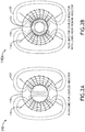
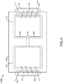
- FIGS. 2A, 2B , 3 , and 4 exemplary embodiments of the coupled output inductor 110, 110A, 110B showing flux lines 120 (e.g., leakage inductance flux lines) according to the inventive concepts disclosed herein are depicted.
- flux lines 120 e.g., leakage inductance flux lines
- the coupled output inductor 110, 110A, 110B may include wire 116 (e.g., magnet wire), a ferromagnetic core (e.g., a toroid core 118 (e.g., an outer toroid core) or a ferromagnetic core 118B), shield material (e.g., ferromagnetic material 124, such as ferrite) and, optionally, one or more inner ferromagnetic cores (e.g., inner toroid cores 122).
- the wire 116 may be wrapped around the ferromagnetic core (e.g., the toroid core 118 (e.g., the outer toroid core) or the ferromagnetic core 118B).
- the ferromagnetic core and/or the one or more inner ferromagnetic cores may be composed of high relative permeability material, such as a ferromagnetic material (e.g., ferrite or molypermalloy).
- a ferromagnetic material e.g., ferrite or molypermalloy
- the flux path (e.g., represented by the flux lines 120) generated by the leakage inductance 112 may be largely in free space around the coupled output inductor 110, 110A, 110B.
- the flux path may interact with nearby electrically-conductive non-ferromagnetic materials, which may attenuate the leakage flux and in turn may reduce the effective leakage inductance 112.
- Some embodiments may include a shielding (e.g., shield material) including at least one ferromagnetic material 124 (which may have a high relative permeability) around (e.g., surrounding or encasing) the coupled output inductor's 110, 110A, 110B ferromagnetic core 118, 118B and/or the one or more inner ferromagnetic core 122, which may minimize such interaction by containing the flux within the shield material. Furthermore, by containing the flux within the shield material, the magnetic field emissions may also be significantly reduced.
- shielding e.g., shield material
- at least one ferromagnetic material 124 which may have a high relative permeability
- the coupled output inductor's 110, 110A, 110B ferromagnetic core 118, 118B and/or the one or more inner ferromagnetic core 122 which may minimize such interaction by containing the flux within the shield material.
- the magnetic field emissions may also be significantly reduced.
- the shielding may provide a higher permeability path for the flux from the leakage inductance 112 to follow, which may result in overall higher leakage inductance 112.
- the permeability of the leakage flux path can be further increased by inserting a stack of smaller inner toroid cores 122 inside the outer toroid core 118, such as illustrated in FIG. 2B .
- shielding e.g., the shield material, such as the ferromagnetic material 124, such as ferrite
- the leakage flux may be contained within the shielding.
- shielding may be similarly applied to the coupled output inductor 110A and 110B.
- Some embodiments including the coupled output inductor 110, 110A, 110B may provide immunity to interaction with nearby electrically-conductive non-ferromagnetic material, significantly reduce magnetic field emissions, and may achieve higher inductances with lower losses in a given volume. Such benefits may lead to higher power density solutions.
- the coupled output inductor 110B may function similarly to the toroid configuration of FIG. 2B .
- the coupled output inductor 110B may include wire 116 (e.g., magnet wire), a ferromagnetic core 118B, and shield material (e.g., ferromagnetic material 124, such as ferrite) that surrounds the ferromagnetic core 118B.
- wire 116 e.g., magnet wire
- shield material e.g., ferromagnetic material 124, such as ferrite
- the ferromagnetic core 118B may be generally rectangular, though in other embodiments, the ferromagnetic core may have any suitable shape. In some embodiments, the ferromagnetic core 118B has identical left and right halves (as shown in FIG. 4 ), though in other embodiments, the ferromagnetic core 118B may be asymmetrical.
- the ferromagnetic core 118B may include outer portions 402 (e.g., outer legs) where the wire 116 is wound around.
- the ferromagnetic core 118B may include at least one inner portion 404 (e.g., an inner leg). The inner portion 404 may be gapped with a gap 406 or may be ungapped.
- the gap 406 or lack of the gap 406 may affect how much leakage flux is allowed to pass through the ferromagnetic core 118B. Some of the flux may pass through a controlled path through the ferromagnetic core 118B and the inner leg, and some of the flux may pass through an uncontrolled path outside of the ferromagnetic core 118B.
- the outer two legs may be wound with the wire 116 to form a coupled inductor.
- the inner leg may provide a path for the leakage flux (similar to the inserted toroid cores 122 in the toroidal configuration of FIG. 2B ). If the inner leg is gapped, the leakage flux may be restricted and may in turn provide better coupling between the two windings. If the inner leg is ungapped, the coupling between windings may weaken, but the leakage flux may be mostly (e.g., almost entirely) contained in the inner leg.
- the outer legs may be gapped, which may weaken the coupling between the windings but may also reduce the overall flux induced by the windings. If the outer legs are gapped, most of the flux induced may become leakage flux, but the total leakage flux would may be decreased since the overall flux is reduced.
- Some embodiments including the coupled output inductor 110, 110A, 110B may allow products to be driven to smaller form factors with higher power capabilities and lower thermal dissipation, which are goals for power converters utilizing current doubler outputs. Some embodiments including the coupled output inductor 110, 110A, 110B may allow for smaller, lighter, and more efficient power solutions for products, such as small-form factor radios with small-form factor power converters.
- embodiments of the inventive concepts disclosed herein may be directed to a system, a power converter, and a coupled output inductor configured to provide a high-permeability path for leakage flux by surrounding a coupled output inductor with high relative permeability material.
- At least one non-transitory computer-readable medium may refer to as at least one non-transitory computer-readable medium (e.g., at least one computer-readable medium implemented as hardware; e.g., at least one non-transitory processor-readable medium, at least one memory (e.g., at least one nonvolatile memory, at least one volatile memory, or a combination thereof; e.g., at least one random-access memory, at least one flash memory, at least one read-only memory (ROM) (e.g., at least one electrically erasable programmable read-only memory (EEPROM)), at least one on-processor memory (e.g., at least one on-processor cache, at least one on-processor buffer, at least one on-processor flash memory, at least one on-processor EEPROM, or a combination thereof), or a combination thereof), at least one storage device (e.g., at least one hard-disk drive, at
- At least one means one or a plurality of; for example, “at least one” may comprise one, two, three, ..., one hundred, or more.
- one or more means one or a plurality of; for example, “one or more” may comprise one, two, three, ..., one hundred, or more.
- zero or more means zero, one, or a plurality of; for example, “zero or more” may comprise zero, one, two, three, ..., one hundred, or more.
- the methods, operations, and/or functionality disclosed may be implemented as sets of instructions or software readable by a device. Further, it is understood that the specific order or hierarchy of steps in the methods, operations, and/or functionality disclosed are examples of exemplary approaches. Based upon design preferences, it is understood that the specific order or hierarchy of steps in the methods, operations, and/or functionality can be rearranged while remaining within the scope of the inventive concepts disclosed herein.
- the accompanying claims may present elements of the various steps in a sample order, and are not necessarily meant to be limited to the specific order or hierarchy presented.
- embodiments of the methods according to the inventive concepts disclosed herein may include one or more of the steps described herein. Further, such steps may be carried out in any desired order and two or more of the steps may be carried out simultaneously with one another. Two or more of the steps disclosed herein may be combined in a single step, and in some embodiments, one or more of the steps may be carried out as two or more sub-steps. Further, other steps or sub-steps may be carried in addition to, or as substitutes to one or more of the steps disclosed herein.
Landscapes
- Engineering & Computer Science (AREA)
- Power Engineering (AREA)
- Chemical & Material Sciences (AREA)
- Composite Materials (AREA)
- Microelectronics & Electronic Packaging (AREA)
- Physics & Mathematics (AREA)
- Electromagnetism (AREA)
- Dc-Dc Converters (AREA)
- Electric Propulsion And Braking For Vehicles (AREA)
- Regulation Of General Use Transformers (AREA)
Abstract
Description
- A power converter using a current doubler output with a coupled output inductor (as opposed to two independent inductors) can be used to reduce the overall size of the power converter. However, in such an application, the common design for a coupled inductor can result in degraded performance and cause the system to suffer from adverse effects.
- Such adverse effects may be present with an existing design of a power converter with a current doubler output that uses a coupled inductor (common magnetic core for multiple inductors) as the output inductor. In such a design, the output inductor is designed to obtain a desired output ripple current by specifying the winding inductance and leakage inductance. In such an existing design, the current ripple can vary significantly, depending on the inductor's proximity to other electrically-conductive non-ferromagnetic materials. For example, an inductor placed very close to an aluminum case could cause the effective leakage inductance to be reduced by 50% or more. This is significant because the current doubler output operates into the leakage inductance of the coupled output inductor and low effective leakage inductance leads to high ripple current.
- Such adverse effects may include significant radiated magnetic field emissions. Radiated emissions from the inductor may also couple into nearby circuitry, causing erroneous behavior or conducted emissions.
- In one aspect, the invention provides a system. The coupled output inductor includes a ferromagnetic core, wire wrapped around the ferromagnetic core, and at least one ferromagnetic path for control of leakage flux. The leakage flux is at least mostly contained within the at least one ferromagnetic path.
- In a further aspect, the invention provides a power converter. The power converter may include a coupled output inductor. The coupled output inductor includes a ferromagnetic core, wire wrapped around the ferromagnetic core, and at least one ferromagnetic path for control of leakage flux. The leakage flux is at least mostly contained within the at least one ferromagnetic path.
- In a further aspect, the invention provides a coupled output inductor. The coupled output inductor includes a ferromagnetic core, wire wrapped around the ferromagnetic core, and at least one ferromagnetic path for control of leakage flux. The leakage flux is at least mostly contained within the at least one ferromagnetic path.
- Implementations of the inventive concepts disclosed herein may be better understood when consideration is given to the following detailed description thereof. Such description makes reference to the included drawings, which are not necessarily to scale, and in which some features may be exaggerated and some features may be omitted or may be represented schematically in the interest of clarity. Like reference numerals in the drawings may represent and refer to the same or similar element, feature, or function. In the drawings:
-
FIG. 1 is a view of an exemplary embodiment of a system implemented according to the inventive concepts disclosed herein. -
FIG. 2A is a view of an exemplary coupled output inductor ofFIG. 1 according to the inventive concepts disclosed herein. -
FIG. 2B is a view of an exemplary coupled output inductor ofFIG. 1 according to the inventive concepts disclosed herein. -
FIG. 3 is a view of the coupled output inductor ofFIG. 2B according to the inventive concepts disclosed herein. -
FIG. 4 is a view of another exemplary coupled output inductor ofFIG. 1 according to the inventive concepts disclosed herein. - Before explaining at least one embodiment of the inventive concepts disclosed herein in detail, it is to be understood that the inventive concepts are not limited in their application to the details of construction and the arrangement of the components or steps or methodologies set forth in the following description or illustrated in the drawings. In the following detailed description of embodiments of the instant inventive concepts, numerous specific details are set forth in order to provide a more thorough understanding of the inventive concepts. However, it will be apparent to one of ordinary skill in the art having the benefit of the instant disclosure that the inventive concepts disclosed herein may be practiced without these specific details. In other instances, well-known features may not be described in detail to avoid unnecessarily complicating the instant disclosure. The inventive concepts disclosed herein are capable of other embodiments or of being practiced or carried out in various ways. Also, it is to be understood that the phraseology and terminology employed herein is for the purpose of description and should not be regarded as limiting.
- As used herein a letter following a reference numeral is intended to reference an embodiment of the feature or element that may be similar, but not necessarily identical, to a previously described element or feature bearing the same reference numeral (e.g., 1, 1a, 1b). Such shorthand notations are used for purposes of convenience only, and should not be construed to limit the inventive concepts disclosed herein in any way unless expressly stated to the contrary.
- Further, unless expressly stated to the contrary, "or" refers to an inclusive or and not to an exclusive or. For example, a condition A or B is satisfied by anyone of the following: A is true (or present) and B is false (or not present), A is false (or not present) and B is true (or present), and both A and B are true (or present).
- In addition, use of the "a" or "an" are employed to describe elements and components of embodiments of the instant inventive concepts. This is done merely for convenience and to give a general sense of the inventive concepts, and "a" and "an" are intended to include one or at least one and the singular also includes the plural unless it is obvious that it is meant otherwise.
- Finally, as used herein any reference to "one embodiment," or "some embodiments" means that a particular element, feature, structure, or characteristic described in connection with the embodiment is included in at least one embodiment of the inventive concepts disclosed herein. The appearances of the phrase "in some embodiments" in various places in the specification are not necessarily all referring to the same embodiment, and embodiments of the inventive concepts disclosed may include one or more of the features expressly described or inherently present herein, or any combination of sub-combination of two or more such features, along with any other features which may not necessarily be expressly described or inherently present in the instant disclosure.
- Broadly, embodiments of the inventive concepts disclosed herein are directed to a system, apparatus, and method to provide a high-permeability path for leakage flux by surrounding a coupled output inductor with high-permeability material (e.g., relative permeability µ/µ0 much greater than 1, such as greater than 10). Some embodiments may provide a solution to provide immunity to nearby conductive materials and reduce magnetic field emissions while reducing part size, core loss, and resistive losses (DCR).
- In some embodiments, a coupled output inductor may provide a high-permeability controlled magnetic path to contain leakage flux from the coupled inductor. The controlled leakage flux path may be a part of the ferromagnetic core, ferromagnetic shielding, one or more additional ferromagnetic cores, or any additional high-permeability material. The coupled output inductor may incorporate a method to control the leakage flux formed at least in part by the shielding and/or ferromagnetic material.
- Referring now to
FIG. 1 , an exemplary embodiment of a system according to the inventive concepts disclosed herein is depicted. For example, the system may be a vehicular system (e.g., an aircraft system) implemented in a vehicle (e.g., an aircraft 100). WhileFIG. 1 exemplarily depicts an aircraft system implemented on theaircraft 100, some embodiments may be implemented as any suitable vehicular system (e.g., an automobile system, a train system, and/or a ship system) including an electronic device that may include a coupled output inductor implemented in any suitable vehicle (e.g., an automobile, a train, and/or a ship). WhileFIG. 1 exemplarily depicts a vehicular system, some embodiments may be implemented as a non-vehicular system. For example, some embodiments may be implemented as any suitable system including any suitable electronic device that may include a coupled output inductor. - The
aircraft 100 may include at least one electronic device (e.g. radio 102), for example, that may use apower converter 104. - The
radio 102 may include at least onepower converter 104. - The
power converter 104 may be implemented as any suitable power converter, such as a push-pull power converter. Thepower converter 104 may include at least one power converter transformer 106 (T) (for simplicity, only the secondary side of the power converter's 104 transformer is schematically shown), one or more (e.g., two) rectifying diodes (D) 108, at least one coupledoutput inductor 110, and output capacitance (C) 114. In some embodiments, the rectifying diodes (D) 108 may be substituted with metal-oxide-semiconductor field-effect transistors (MosFETs) as controlled switches. Thepower converter 104 may be configured to include a current doubler output by using the coupledoutput inductor 110. LLeakage represents theleakage inductance 112 of the coupledoutput inductor 110. - In some embodiments including the coupled
output inductor 110, energy is not stored in the portion of the core associated with mutual inductance. The energy is stored in the magnetic field associated with theleakage inductance 112, which is largely in the free space around the core of the coupledoutput inductor 110. - Referring now to
FIGS. 2A, 2B ,3 , and4 , exemplary embodiments of the coupledoutput inductor output inductor ferromagnetic core 118B), shield material (e.g.,ferromagnetic material 124, such as ferrite) and, optionally, one or more inner ferromagnetic cores (e.g., inner toroid cores 122). Thewire 116 may be wrapped around the ferromagnetic core (e.g., the toroid core 118 (e.g., the outer toroid core) or theferromagnetic core 118B). - The ferromagnetic core and/or the one or more inner ferromagnetic cores may be composed of high relative permeability material, such as a ferromagnetic material (e.g., ferrite or molypermalloy).
- The flux path (e.g., represented by the flux lines 120) generated by the
leakage inductance 112 may be largely in free space around the coupledoutput inductor effective leakage inductance 112. Some embodiments may include a shielding (e.g., shield material) including at least one ferromagnetic material 124 (which may have a high relative permeability) around (e.g., surrounding or encasing) the coupled output inductor's 110, 110A, 110Bferromagnetic core ferromagnetic core 122, which may minimize such interaction by containing the flux within the shield material. Furthermore, by containing the flux within the shield material, the magnetic field emissions may also be significantly reduced. - An additional benefit of the shielding is that the shielding may provide a higher permeability path for the flux from the
leakage inductance 112 to follow, which may result in overallhigher leakage inductance 112. - Furthermore, in some embodiments, with the coupled
output inductor wire 116 wound on acommon toroid core 118, the permeability of the leakage flux path can be further increased by inserting a stack of smallerinner toroid cores 122 inside theouter toroid core 118, such as illustrated inFIG. 2B . - As shown in
FIG. 3 , which shows a cross-section of the coupledoutput inductor 110A, in some embodiments, just as the leakage flux may flow through the higher permeability path provided by theinner toroid cores 118, when shielding (e.g., the shield material, such as theferromagnetic material 124, such as ferrite) is added, the leakage flux may be contained within the shielding. In some embodiments, shielding may be similarly applied to the coupledoutput inductor - Some embodiments including the coupled
output inductor - As shown in
FIG. 4 , an exemplary embodiment of the coupledoutput inductor 110B showingflux lines 120 according to the inventive concepts disclosed herein is depicted. The coupledoutput inductor 110B may function similarly to the toroid configuration ofFIG. 2B . The coupledoutput inductor 110B may include wire 116 (e.g., magnet wire), aferromagnetic core 118B, and shield material (e.g.,ferromagnetic material 124, such as ferrite) that surrounds theferromagnetic core 118B. - In some embodiments, the
ferromagnetic core 118B may be generally rectangular, though in other embodiments, the ferromagnetic core may have any suitable shape. In some embodiments, theferromagnetic core 118B has identical left and right halves (as shown inFIG. 4 ), though in other embodiments, theferromagnetic core 118B may be asymmetrical. Theferromagnetic core 118B may include outer portions 402 (e.g., outer legs) where thewire 116 is wound around. Theferromagnetic core 118B may include at least one inner portion 404 (e.g., an inner leg). Theinner portion 404 may be gapped with a gap 406 or may be ungapped. The gap 406 or lack of the gap 406 may affect how much leakage flux is allowed to pass through theferromagnetic core 118B. Some of the flux may pass through a controlled path through theferromagnetic core 118B and the inner leg, and some of the flux may pass through an uncontrolled path outside of theferromagnetic core 118B. - Still referring to
FIG. 4 , the outer two legs may be wound with thewire 116 to form a coupled inductor. The inner leg may provide a path for the leakage flux (similar to the insertedtoroid cores 122 in the toroidal configuration ofFIG. 2B ). If the inner leg is gapped, the leakage flux may be restricted and may in turn provide better coupling between the two windings. If the inner leg is ungapped, the coupling between windings may weaken, but the leakage flux may be mostly (e.g., almost entirely) contained in the inner leg. - In some embodiments, the outer legs may be gapped, which may weaken the coupling between the windings but may also reduce the overall flux induced by the windings. If the outer legs are gapped, most of the flux induced may become leakage flux, but the total leakage flux would may be decreased since the overall flux is reduced.
- Some embodiments including the coupled
output inductor output inductor - As will be appreciated from the above, embodiments of the inventive concepts disclosed herein may be directed to a system, a power converter, and a coupled output inductor configured to provide a high-permeability path for leakage flux by surrounding a coupled output inductor with high relative permeability material.
- As used throughout and as would be appreciated by those skilled in the art, "at least one non-transitory computer-readable medium" may refer to as at least one non-transitory computer-readable medium (e.g., at least one computer-readable medium implemented as hardware; e.g., at least one non-transitory processor-readable medium, at least one memory (e.g., at least one nonvolatile memory, at least one volatile memory, or a combination thereof; e.g., at least one random-access memory, at least one flash memory, at least one read-only memory (ROM) (e.g., at least one electrically erasable programmable read-only memory (EEPROM)), at least one on-processor memory (e.g., at least one on-processor cache, at least one on-processor buffer, at least one on-processor flash memory, at least one on-processor EEPROM, or a combination thereof), or a combination thereof), at least one storage device (e.g., at least one hard-disk drive, at least one tape drive, at least one solid-state drive, at least one flash drive, at least one readable and/or writable disk of at least one optical drive configured to read from and/or write to the at least one readable and/or writable disk, or a combination thereof), or a combination thereof).
- As used throughout, "at least one" means one or a plurality of; for example, "at least one" may comprise one, two, three, ..., one hundred, or more. Similarly, as used throughout, "one or more" means one or a plurality of; for example, "one or more" may comprise one, two, three, ..., one hundred, or more. Further, as used throughout, "zero or more" means zero, one, or a plurality of; for example, "zero or more" may comprise zero, one, two, three, ..., one hundred, or more.
- In the present disclosure, the methods, operations, and/or functionality disclosed may be implemented as sets of instructions or software readable by a device. Further, it is understood that the specific order or hierarchy of steps in the methods, operations, and/or functionality disclosed are examples of exemplary approaches. Based upon design preferences, it is understood that the specific order or hierarchy of steps in the methods, operations, and/or functionality can be rearranged while remaining within the scope of the inventive concepts disclosed herein. The accompanying claims may present elements of the various steps in a sample order, and are not necessarily meant to be limited to the specific order or hierarchy presented.
- It is to be understood that embodiments of the methods according to the inventive concepts disclosed herein may include one or more of the steps described herein. Further, such steps may be carried out in any desired order and two or more of the steps may be carried out simultaneously with one another. Two or more of the steps disclosed herein may be combined in a single step, and in some embodiments, one or more of the steps may be carried out as two or more sub-steps. Further, other steps or sub-steps may be carried in addition to, or as substitutes to one or more of the steps disclosed herein.
- From the above description, it is clear that the inventive concepts disclosed herein are well adapted to carry out the objects and to attain the advantages mentioned herein as well as those inherent in the inventive concepts disclosed herein. While presently preferred embodiments of the inventive concepts disclosed herein have been described for purposes of this disclosure, it will be understood that numerous changes may be made which will readily suggest themselves to those skilled in the art and which are accomplished within the broad scope and coverage of the inventive concepts disclosed and claimed herein.
Claims (15)
- A coupled output inductor, comprising:a ferromagnetic core (118); andwire (116) wrapped around the ferromagnetic core; andat least one ferromagnetic path for control of leakage flux,wherein the leakage flux is at least mostly contained within the at least one ferromagnetic path.
- The coupled output inductor of claim 1, wherein the ferromagnetic core is at least composed of at least one of ferrite or molypermalloy.
- The coupled output inductor of claim 1 or 2, wherein the at least one ferromagnetic path comprises shielding surrounding the ferromagnetic core, wherein the shielding is composed of a ferromagnetic material (124).
- The coupled output inductor of claim 3, wherein the shielding is at least composed of ferrite, and/orwherein the at least one ferromagnetic path is formed at least in part by the shielding, and/orwherein the shielding reduces magnetic field emissions as compared to a coupled output inductor without the shielding, and/orwherein the shielding provides a path for the leakage flux to flow, which results in overall higher leakage inductance as compared to a coupled output inductor without the shielding.
- The coupled output inductor of any preceding claim, wherein the ferromagnetic core is a toroid core.
- The coupled output inductor of claim 5, wherein the toroid core is an outer toroid core, wherein the at least one ferromagnetic path further comprises:at least one inner toroid core implemented inside a hole of the outer toroid core, and optionallywherein the at least one inner toroid core comprises a stack of inner toroid cores.
- The system of claim 6, wherein the at least one ferromagnetic path is formed at least in part by the at least one inner toroid core.
- The coupled output inductor of any preceding claim, wherein the ferromagnetic core includes outer legs (402) and an inner leg (404), wherein the wire is wrapped around the outer legs of the ferromagnetic core, wherein the at least one ferromagnetic path comprises the inner leg.
- The system of claim 8, wherein the inner leg is gapped (406).
- A system, comprising:a coupled output inductor (110) according to any preceding claim.
- The system of claim 10, further comprising a power converter (104), wherein the power converter comprises the coupled output inductor (110).
- The system of claim 11, further comprising an electronic device comprising the power converter.
- The system of claim 11 or 12, wherein the power converter is implemented in a vehicle (100).
- The system of claim 11, 12 or 13, wherein the power converter further comprises at least one transformer (106) and at least one rectifying diode (108), the at least one transformer coupled to the at least one rectifying diode, the at least one rectifying diode coupled to the coupled output inductor (110).
- The system of claims 11 to 14, wherein the power converter is configured to include a current doubler output by using the coupled output inductor.
Applications Claiming Priority (1)
| Application Number | Priority Date | Filing Date | Title |
|---|---|---|---|
| US16/521,182 US20210210281A1 (en) | 2019-07-24 | 2019-07-24 | Coupled Output Inductor and System |
Publications (2)
| Publication Number | Publication Date |
|---|---|
| EP3770928A1 true EP3770928A1 (en) | 2021-01-27 |
| EP3770928B1 EP3770928B1 (en) | 2023-10-11 |
Family
ID=71783952
Family Applications (1)
| Application Number | Title | Priority Date | Filing Date |
|---|---|---|---|
| EP20187494.8A Active EP3770928B1 (en) | 2019-07-24 | 2020-07-23 | Coupled output inductor and system |
Country Status (2)
| Country | Link |
|---|---|
| US (1) | US20210210281A1 (en) |
| EP (1) | EP3770928B1 (en) |
Citations (4)
| Publication number | Priority date | Publication date | Assignee | Title |
|---|---|---|---|---|
| KR100732612B1 (en) * | 2006-02-07 | 2007-06-27 | 학교법인 포항공과대학교 | High Efficiency Step-Down DC-DC Converters for Hybrid Vehicles |
| US20090185398A1 (en) * | 2007-06-30 | 2009-07-23 | Cuks, Llc | Integrated magnetics switching converter with zero inductor and output ripple currents and lossless switching |
| US20100254168A1 (en) * | 2009-03-31 | 2010-10-07 | Sriram Chandrasekaran | Magnetic Device Formed with U-Shaped Core Pieces and Power Converter Employing the Same |
| EP2299456A1 (en) * | 2009-09-17 | 2011-03-23 | DET International Holding Limited | Integrated magnetic component |
Family Cites Families (1)
| Publication number | Priority date | Publication date | Assignee | Title |
|---|---|---|---|---|
| JPH0746664B2 (en) * | 1992-06-19 | 1995-05-17 | 日本▲まき▼線工業株式会社 | Magnetic shield structure of toroidal transformer |
-
2019
- 2019-07-24 US US16/521,182 patent/US20210210281A1/en not_active Abandoned
-
2020
- 2020-07-23 EP EP20187494.8A patent/EP3770928B1/en active Active
Patent Citations (4)
| Publication number | Priority date | Publication date | Assignee | Title |
|---|---|---|---|---|
| KR100732612B1 (en) * | 2006-02-07 | 2007-06-27 | 학교법인 포항공과대학교 | High Efficiency Step-Down DC-DC Converters for Hybrid Vehicles |
| US20090185398A1 (en) * | 2007-06-30 | 2009-07-23 | Cuks, Llc | Integrated magnetics switching converter with zero inductor and output ripple currents and lossless switching |
| US20100254168A1 (en) * | 2009-03-31 | 2010-10-07 | Sriram Chandrasekaran | Magnetic Device Formed with U-Shaped Core Pieces and Power Converter Employing the Same |
| EP2299456A1 (en) * | 2009-09-17 | 2011-03-23 | DET International Holding Limited | Integrated magnetic component |
Non-Patent Citations (2)
| Title |
|---|
| KEVIN J HARTNETT ET AL: "CCTT-Core Split-Winding Integrated Magnetic for High-Power DC DC Converters", IEEE TRANSACTIONS ON POWER ELECTRONICS, INSTITUTE OF ELECTRICAL AND ELECTRONICS ENGINEERS, USA, vol. 28, no. 11, 1 November 2013 (2013-11-01), pages 4970 - 4984, XP011507702, ISSN: 0885-8993, DOI: 10.1109/TPEL.2013.2240394 * |
| PENG XU ET AL: "Design of high-input voltage regulator modules with a novel integrated magnetics", APEC 2001. 16TH. ANNUAL IEEE APPLIED POWER ELECTRONICS CONFERENCE AND EXPOSITION. ANAHEIM, CA, MARCH 4 - 8, 2001; [ANNUAL APPLIED POWER ELECTRONICS CONFERENCE], NEW YORK, NY : IEEE, US, vol. 1, 4 March 2001 (2001-03-04), pages 262 - 267, XP010536005, ISBN: 978-0-7803-6618-3 * |
Also Published As
| Publication number | Publication date |
|---|---|
| US20210210281A1 (en) | 2021-07-08 |
| EP3770928B1 (en) | 2023-10-11 |
Similar Documents
| Publication | Publication Date | Title |
|---|---|---|
| EP2624260B1 (en) | Forward converter with magnetic component | |
| US8487733B2 (en) | Composite magnetic core assembly, magnetic element and fabricating method thereof | |
| KR0165948B1 (en) | Choke coil | |
| US10083791B2 (en) | Integrated magnetics for soft switching converter | |
| US8766756B2 (en) | Transverse shroud and bobbin assembly | |
| JPWO2018173900A1 (en) | Reactor, power circuit | |
| US20170117091A1 (en) | Power converter transformer with reduced leakage inductance | |
| US9799440B2 (en) | Coupled inductor | |
| US12266462B2 (en) | Reactor and multi-phase interleave-type DC-DC converter | |
| EP2771891B2 (en) | Inductive component and use | |
| US20120223795A1 (en) | Shroud for bobbin | |
| US11205537B2 (en) | Magnetic component, resonant electrical circuit, electrical converter and electrical system | |
| CN110832607A (en) | Memory choke | |
| US5635890A (en) | Choke coil | |
| EP3770928B1 (en) | Coupled output inductor and system | |
| JP2017073486A (en) | Coil parts | |
| KR20220101193A (en) | Magnetic components with electrically variable properties | |
| CN213905093U (en) | Inductor core assembly and inductor including the same | |
| JPH04230009A (en) | Choke or transformer | |
| US5726618A (en) | Planar transductor | |
| GB2361110A (en) | An induction device | |
| US5825272A (en) | Choke coil for suppressing common-mode noise and normal-mode noise | |
| JPH075617Y2 (en) | Electromagnetic device | |
| JPH11135332A (en) | Variable inductance transformer | |
| JP3079071B2 (en) | Inductance element with gap |
Legal Events
| Date | Code | Title | Description |
|---|---|---|---|
| PUAI | Public reference made under article 153(3) epc to a published international application that has entered the european phase |
Free format text: ORIGINAL CODE: 0009012 |
|
| STAA | Information on the status of an ep patent application or granted ep patent |
Free format text: STATUS: THE APPLICATION HAS BEEN PUBLISHED |
|
| AK | Designated contracting states |
Kind code of ref document: A1 Designated state(s): AL AT BE BG CH CY CZ DE DK EE ES FI FR GB GR HR HU IE IS IT LI LT LU LV MC MK MT NL NO PL PT RO RS SE SI SK SM TR |
|
| AX | Request for extension of the european patent |
Extension state: BA ME |
|
| STAA | Information on the status of an ep patent application or granted ep patent |
Free format text: STATUS: REQUEST FOR EXAMINATION WAS MADE |
|
| 17P | Request for examination filed |
Effective date: 20210727 |
|
| RBV | Designated contracting states (corrected) |
Designated state(s): AL AT BE BG CH CY CZ DE DK EE ES FI FR GB GR HR HU IE IS IT LI LT LU LV MC MK MT NL NO PL PT RO RS SE SI SK SM TR |
|
| RIC1 | Information provided on ipc code assigned before grant |
Ipc: H02M 1/44 20070101ALI20230320BHEP Ipc: H02M 3/337 20060101ALI20230320BHEP Ipc: H01F 27/34 20060101ALI20230320BHEP Ipc: H01F 3/10 20060101AFI20230320BHEP |
|
| GRAP | Despatch of communication of intention to grant a patent |
Free format text: ORIGINAL CODE: EPIDOSNIGR1 |
|
| STAA | Information on the status of an ep patent application or granted ep patent |
Free format text: STATUS: GRANT OF PATENT IS INTENDED |
|
| INTG | Intention to grant announced |
Effective date: 20230519 |
|
| RIN1 | Information on inventor provided before grant (corrected) |
Inventor name: WEISS, JEREMY Inventor name: DEHOTAL, JAROD Inventor name: LUCAS, JOHNNY Inventor name: DEWALD, JUSTIN |
|
| GRAS | Grant fee paid |
Free format text: ORIGINAL CODE: EPIDOSNIGR3 |
|
| GRAA | (expected) grant |
Free format text: ORIGINAL CODE: 0009210 |
|
| STAA | Information on the status of an ep patent application or granted ep patent |
Free format text: STATUS: THE PATENT HAS BEEN GRANTED |
|
| AK | Designated contracting states |
Kind code of ref document: B1 Designated state(s): AL AT BE BG CH CY CZ DE DK EE ES FI FR GB GR HR HU IE IS IT LI LT LU LV MC MK MT NL NO PL PT RO RS SE SI SK SM TR |
|
| REG | Reference to a national code |
Ref country code: GB Ref legal event code: FG4D |
|
| REG | Reference to a national code |
Ref country code: CH Ref legal event code: EP |
|
| REG | Reference to a national code |
Ref country code: DE Ref legal event code: R096 Ref document number: 602020018930 Country of ref document: DE |
|
| REG | Reference to a national code |
Ref country code: IE Ref legal event code: FG4D |
|
| REG | Reference to a national code |
Ref country code: LT Ref legal event code: MG9D |
|
| REG | Reference to a national code |
Ref country code: NL Ref legal event code: MP Effective date: 20231011 |
|
| REG | Reference to a national code |
Ref country code: AT Ref legal event code: MK05 Ref document number: 1621078 Country of ref document: AT Kind code of ref document: T Effective date: 20231011 |
|
| PG25 | Lapsed in a contracting state [announced via postgrant information from national office to epo] |
Ref country code: NL Free format text: LAPSE BECAUSE OF FAILURE TO SUBMIT A TRANSLATION OF THE DESCRIPTION OR TO PAY THE FEE WITHIN THE PRESCRIBED TIME-LIMIT Effective date: 20231011 |
|
| PG25 | Lapsed in a contracting state [announced via postgrant information from national office to epo] |
Ref country code: GR Free format text: LAPSE BECAUSE OF FAILURE TO SUBMIT A TRANSLATION OF THE DESCRIPTION OR TO PAY THE FEE WITHIN THE PRESCRIBED TIME-LIMIT Effective date: 20240112 |
|
| PG25 | Lapsed in a contracting state [announced via postgrant information from national office to epo] |
Ref country code: IS Free format text: LAPSE BECAUSE OF FAILURE TO SUBMIT A TRANSLATION OF THE DESCRIPTION OR TO PAY THE FEE WITHIN THE PRESCRIBED TIME-LIMIT Effective date: 20240211 |
|
| PG25 | Lapsed in a contracting state [announced via postgrant information from national office to epo] |
Ref country code: LT Free format text: LAPSE BECAUSE OF FAILURE TO SUBMIT A TRANSLATION OF THE DESCRIPTION OR TO PAY THE FEE WITHIN THE PRESCRIBED TIME-LIMIT Effective date: 20231011 |
|
| PG25 | Lapsed in a contracting state [announced via postgrant information from national office to epo] |
Ref country code: AT Free format text: LAPSE BECAUSE OF FAILURE TO SUBMIT A TRANSLATION OF THE DESCRIPTION OR TO PAY THE FEE WITHIN THE PRESCRIBED TIME-LIMIT Effective date: 20231011 |
|
| PG25 | Lapsed in a contracting state [announced via postgrant information from national office to epo] |
Ref country code: ES Free format text: LAPSE BECAUSE OF FAILURE TO SUBMIT A TRANSLATION OF THE DESCRIPTION OR TO PAY THE FEE WITHIN THE PRESCRIBED TIME-LIMIT Effective date: 20231011 |
|
| PG25 | Lapsed in a contracting state [announced via postgrant information from national office to epo] |
Ref country code: LT Free format text: LAPSE BECAUSE OF FAILURE TO SUBMIT A TRANSLATION OF THE DESCRIPTION OR TO PAY THE FEE WITHIN THE PRESCRIBED TIME-LIMIT Effective date: 20231011 Ref country code: IS Free format text: LAPSE BECAUSE OF FAILURE TO SUBMIT A TRANSLATION OF THE DESCRIPTION OR TO PAY THE FEE WITHIN THE PRESCRIBED TIME-LIMIT Effective date: 20240211 Ref country code: GR Free format text: LAPSE BECAUSE OF FAILURE TO SUBMIT A TRANSLATION OF THE DESCRIPTION OR TO PAY THE FEE WITHIN THE PRESCRIBED TIME-LIMIT Effective date: 20240112 Ref country code: ES Free format text: LAPSE BECAUSE OF FAILURE TO SUBMIT A TRANSLATION OF THE DESCRIPTION OR TO PAY THE FEE WITHIN THE PRESCRIBED TIME-LIMIT Effective date: 20231011 Ref country code: BG Free format text: LAPSE BECAUSE OF FAILURE TO SUBMIT A TRANSLATION OF THE DESCRIPTION OR TO PAY THE FEE WITHIN THE PRESCRIBED TIME-LIMIT Effective date: 20240111 Ref country code: AT Free format text: LAPSE BECAUSE OF FAILURE TO SUBMIT A TRANSLATION OF THE DESCRIPTION OR TO PAY THE FEE WITHIN THE PRESCRIBED TIME-LIMIT Effective date: 20231011 Ref country code: PT Free format text: LAPSE BECAUSE OF FAILURE TO SUBMIT A TRANSLATION OF THE DESCRIPTION OR TO PAY THE FEE WITHIN THE PRESCRIBED TIME-LIMIT Effective date: 20240212 |
|
| PG25 | Lapsed in a contracting state [announced via postgrant information from national office to epo] |
Ref country code: SE Free format text: LAPSE BECAUSE OF FAILURE TO SUBMIT A TRANSLATION OF THE DESCRIPTION OR TO PAY THE FEE WITHIN THE PRESCRIBED TIME-LIMIT Effective date: 20231011 Ref country code: RS Free format text: LAPSE BECAUSE OF FAILURE TO SUBMIT A TRANSLATION OF THE DESCRIPTION OR TO PAY THE FEE WITHIN THE PRESCRIBED TIME-LIMIT Effective date: 20231011 Ref country code: PL Free format text: LAPSE BECAUSE OF FAILURE TO SUBMIT A TRANSLATION OF THE DESCRIPTION OR TO PAY THE FEE WITHIN THE PRESCRIBED TIME-LIMIT Effective date: 20231011 Ref country code: NO Free format text: LAPSE BECAUSE OF FAILURE TO SUBMIT A TRANSLATION OF THE DESCRIPTION OR TO PAY THE FEE WITHIN THE PRESCRIBED TIME-LIMIT Effective date: 20240111 Ref country code: LV Free format text: LAPSE BECAUSE OF FAILURE TO SUBMIT A TRANSLATION OF THE DESCRIPTION OR TO PAY THE FEE WITHIN THE PRESCRIBED TIME-LIMIT Effective date: 20231011 Ref country code: HR Free format text: LAPSE BECAUSE OF FAILURE TO SUBMIT A TRANSLATION OF THE DESCRIPTION OR TO PAY THE FEE WITHIN THE PRESCRIBED TIME-LIMIT Effective date: 20231011 |
|
| PG25 | Lapsed in a contracting state [announced via postgrant information from national office to epo] |
Ref country code: DK Free format text: LAPSE BECAUSE OF FAILURE TO SUBMIT A TRANSLATION OF THE DESCRIPTION OR TO PAY THE FEE WITHIN THE PRESCRIBED TIME-LIMIT Effective date: 20231011 |
|
| REG | Reference to a national code |
Ref country code: DE Ref legal event code: R097 Ref document number: 602020018930 Country of ref document: DE |
|
| PG25 | Lapsed in a contracting state [announced via postgrant information from national office to epo] |
Ref country code: CZ Free format text: LAPSE BECAUSE OF FAILURE TO SUBMIT A TRANSLATION OF THE DESCRIPTION OR TO PAY THE FEE WITHIN THE PRESCRIBED TIME-LIMIT Effective date: 20231011 |
|
| PG25 | Lapsed in a contracting state [announced via postgrant information from national office to epo] |
Ref country code: SK Free format text: LAPSE BECAUSE OF FAILURE TO SUBMIT A TRANSLATION OF THE DESCRIPTION OR TO PAY THE FEE WITHIN THE PRESCRIBED TIME-LIMIT Effective date: 20231011 |
|
| PG25 | Lapsed in a contracting state [announced via postgrant information from national office to epo] |
Ref country code: SM Free format text: LAPSE BECAUSE OF FAILURE TO SUBMIT A TRANSLATION OF THE DESCRIPTION OR TO PAY THE FEE WITHIN THE PRESCRIBED TIME-LIMIT Effective date: 20231011 Ref country code: SK Free format text: LAPSE BECAUSE OF FAILURE TO SUBMIT A TRANSLATION OF THE DESCRIPTION OR TO PAY THE FEE WITHIN THE PRESCRIBED TIME-LIMIT Effective date: 20231011 Ref country code: RO Free format text: LAPSE BECAUSE OF FAILURE TO SUBMIT A TRANSLATION OF THE DESCRIPTION OR TO PAY THE FEE WITHIN THE PRESCRIBED TIME-LIMIT Effective date: 20231011 Ref country code: IT Free format text: LAPSE BECAUSE OF FAILURE TO SUBMIT A TRANSLATION OF THE DESCRIPTION OR TO PAY THE FEE WITHIN THE PRESCRIBED TIME-LIMIT Effective date: 20231011 Ref country code: EE Free format text: LAPSE BECAUSE OF FAILURE TO SUBMIT A TRANSLATION OF THE DESCRIPTION OR TO PAY THE FEE WITHIN THE PRESCRIBED TIME-LIMIT Effective date: 20231011 Ref country code: DK Free format text: LAPSE BECAUSE OF FAILURE TO SUBMIT A TRANSLATION OF THE DESCRIPTION OR TO PAY THE FEE WITHIN THE PRESCRIBED TIME-LIMIT Effective date: 20231011 Ref country code: CZ Free format text: LAPSE BECAUSE OF FAILURE TO SUBMIT A TRANSLATION OF THE DESCRIPTION OR TO PAY THE FEE WITHIN THE PRESCRIBED TIME-LIMIT Effective date: 20231011 |
|
| PLBE | No opposition filed within time limit |
Free format text: ORIGINAL CODE: 0009261 |
|
| STAA | Information on the status of an ep patent application or granted ep patent |
Free format text: STATUS: NO OPPOSITION FILED WITHIN TIME LIMIT |
|
| 26N | No opposition filed |
Effective date: 20240712 |
|
| PG25 | Lapsed in a contracting state [announced via postgrant information from national office to epo] |
Ref country code: SI Free format text: LAPSE BECAUSE OF FAILURE TO SUBMIT A TRANSLATION OF THE DESCRIPTION OR TO PAY THE FEE WITHIN THE PRESCRIBED TIME-LIMIT Effective date: 20231011 |
|
| PG25 | Lapsed in a contracting state [announced via postgrant information from national office to epo] |
Ref country code: SI Free format text: LAPSE BECAUSE OF FAILURE TO SUBMIT A TRANSLATION OF THE DESCRIPTION OR TO PAY THE FEE WITHIN THE PRESCRIBED TIME-LIMIT Effective date: 20231011 |
|
| PG25 | Lapsed in a contracting state [announced via postgrant information from national office to epo] |
Ref country code: MC Free format text: LAPSE BECAUSE OF FAILURE TO SUBMIT A TRANSLATION OF THE DESCRIPTION OR TO PAY THE FEE WITHIN THE PRESCRIBED TIME-LIMIT Effective date: 20231011 |
|
| REG | Reference to a national code |
Ref country code: CH Ref legal event code: PL |
|
| PG25 | Lapsed in a contracting state [announced via postgrant information from national office to epo] |
Ref country code: LU Free format text: LAPSE BECAUSE OF NON-PAYMENT OF DUE FEES Effective date: 20240723 |
|
| PG25 | Lapsed in a contracting state [announced via postgrant information from national office to epo] |
Ref country code: LU Free format text: LAPSE BECAUSE OF NON-PAYMENT OF DUE FEES Effective date: 20240723 |
|
| PG25 | Lapsed in a contracting state [announced via postgrant information from national office to epo] |
Ref country code: BE Free format text: LAPSE BECAUSE OF NON-PAYMENT OF DUE FEES Effective date: 20240731 Ref country code: CH Free format text: LAPSE BECAUSE OF NON-PAYMENT OF DUE FEES Effective date: 20240731 |
|
| REG | Reference to a national code |
Ref country code: BE Ref legal event code: MM Effective date: 20240731 |
|
| PGFP | Annual fee paid to national office [announced via postgrant information from national office to epo] |
Ref country code: GB Payment date: 20250619 Year of fee payment: 6 |
|
| PGFP | Annual fee paid to national office [announced via postgrant information from national office to epo] |
Ref country code: FR Payment date: 20250620 Year of fee payment: 6 |
|
| PG25 | Lapsed in a contracting state [announced via postgrant information from national office to epo] |
Ref country code: IE Free format text: LAPSE BECAUSE OF NON-PAYMENT OF DUE FEES Effective date: 20240723 |
|
| PG25 | Lapsed in a contracting state [announced via postgrant information from national office to epo] |
Ref country code: FI Free format text: LAPSE BECAUSE OF FAILURE TO SUBMIT A TRANSLATION OF THE DESCRIPTION OR TO PAY THE FEE WITHIN THE PRESCRIBED TIME-LIMIT Effective date: 20231011 |
|
| PGFP | Annual fee paid to national office [announced via postgrant information from national office to epo] |
Ref country code: DE Payment date: 20250620 Year of fee payment: 6 |
|
| P01 | Opt-out of the competence of the unified patent court (upc) registered |
Free format text: CASE NUMBER: UPC_APP_0018650_3770928/2025 Effective date: 20251221 |
|
| PG25 | Lapsed in a contracting state [announced via postgrant information from national office to epo] |
Ref country code: CY Free format text: LAPSE BECAUSE OF FAILURE TO SUBMIT A TRANSLATION OF THE DESCRIPTION OR TO PAY THE FEE WITHIN THE PRESCRIBED TIME-LIMIT; INVALID AB INITIO Effective date: 20200723 |
|
| PG25 | Lapsed in a contracting state [announced via postgrant information from national office to epo] |
Ref country code: HU Free format text: LAPSE BECAUSE OF FAILURE TO SUBMIT A TRANSLATION OF THE DESCRIPTION OR TO PAY THE FEE WITHIN THE PRESCRIBED TIME-LIMIT; INVALID AB INITIO Effective date: 20200723 |