EP3770753A1 - Program generation unit, information processing device, program generation method, and program - Google Patents
Program generation unit, information processing device, program generation method, and program Download PDFInfo
- Publication number
- EP3770753A1 EP3770753A1 EP19771160.9A EP19771160A EP3770753A1 EP 3770753 A1 EP3770753 A1 EP 3770753A1 EP 19771160 A EP19771160 A EP 19771160A EP 3770753 A1 EP3770753 A1 EP 3770753A1
- Authority
- EP
- European Patent Office
- Prior art keywords
- voltage value
- program
- core
- command
- voltage
- Prior art date
- Legal status (The legal status is an assumption and is not a legal conclusion. Google has not performed a legal analysis and makes no representation as to the accuracy of the status listed.)
- Granted
Links
Images



Classifications
-
- G—PHYSICS
- G06—COMPUTING OR CALCULATING; COUNTING
- G06F—ELECTRIC DIGITAL DATA PROCESSING
- G06F8/00—Arrangements for software engineering
- G06F8/40—Transformation of program code
- G06F8/54—Link editing before load time
-
- G—PHYSICS
- G06—COMPUTING OR CALCULATING; COUNTING
- G06F—ELECTRIC DIGITAL DATA PROCESSING
- G06F1/00—Details not covered by groups G06F3/00 - G06F13/00 and G06F21/00
- G06F1/26—Power supply means, e.g. regulation thereof
- G06F1/32—Means for saving power
- G06F1/3203—Power management, i.e. event-based initiation of a power-saving mode
- G06F1/3234—Power saving characterised by the action undertaken
- G06F1/3296—Power saving characterised by the action undertaken by lowering the supply or operating voltage
-
- G—PHYSICS
- G06—COMPUTING OR CALCULATING; COUNTING
- G06F—ELECTRIC DIGITAL DATA PROCESSING
- G06F8/00—Arrangements for software engineering
- G06F8/40—Transformation of program code
- G06F8/41—Compilation
- G06F8/44—Encoding
- G06F8/447—Target code generation
-
- G—PHYSICS
- G06—COMPUTING OR CALCULATING; COUNTING
- G06F—ELECTRIC DIGITAL DATA PROCESSING
- G06F8/00—Arrangements for software engineering
- G06F8/40—Transformation of program code
- G06F8/41—Compilation
-
- Y—GENERAL TAGGING OF NEW TECHNOLOGICAL DEVELOPMENTS; GENERAL TAGGING OF CROSS-SECTIONAL TECHNOLOGIES SPANNING OVER SEVERAL SECTIONS OF THE IPC; TECHNICAL SUBJECTS COVERED BY FORMER USPC CROSS-REFERENCE ART COLLECTIONS [XRACs] AND DIGESTS
- Y02—TECHNOLOGIES OR APPLICATIONS FOR MITIGATION OR ADAPTATION AGAINST CLIMATE CHANGE
- Y02D—CLIMATE CHANGE MITIGATION TECHNOLOGIES IN INFORMATION AND COMMUNICATION TECHNOLOGIES [ICT], I.E. INFORMATION AND COMMUNICATION TECHNOLOGIES AIMING AT THE REDUCTION OF THEIR OWN ENERGY USE
- Y02D10/00—Energy efficient computing, e.g. low power processors, power management or thermal management
Definitions
- the present invention relates to a program generation unit, an information processing device, a program generation method, and a program.
- Patent Document 1 and Patent Document 2 disclose the feature of changing operating voltage values in order to control the power consumption so as to be reduced.
- Patent Document 1 discloses the feature of changing operating voltage values based on power contexts in which power control information is stored for each program.
- Patent Document 1 changes the operating voltage values when executing programs based on success rates or failure rates in the power control information, which are power contexts.
- a program in order to generate power contexts, a program must be executed at least once in order to check the success rate or the failure rate in advance, and changing the operating voltage values in accordance with user programs creates a burden.
- Patent Document 2 if a set of commands in which the same minimum operating voltage value command occurs consecutively is detected, then the operating voltage values are changed when a program is executed.
- an example objective of the present invention is to provide a program generation unit, an information processing device, a program generation method, and a program in which changing operating voltage values in accordance with user programs does not tend to create a burden.
- a program generation unit generates voltage value information for making an LSI run on an operating voltage value based on a voltage context.
- the program generation unit includes: a first compiler configured to compile a source program and that generates an object including a command sequence; a second compiler configured to generate the voltage value information based on a command density in the command sequence; and a linker configure to link the object with the voltage value information and that generates a user program.
- a program generation method generates voltage value information for making an LSI run on an operating voltage value based on a voltage context.
- the program generation method includes: compiling a source program and generating an object including a command sequence; generating the voltage value information based on a command density in the command sequence; and linking the object with the voltage value information and generating a user program.
- a program makes a computer generate voltage value information for making an LSI run on an operating voltage value based on a voltage context, wherein the program makes the computer execute processes.
- the process includes: compiling a source program and generating an object including a command sequence; generating the voltage value information based on a command density in the command sequence; and linking the object with the voltage value information and generating a user program.
- changing operating voltage values in accordance with user programs does not tend to create a burden.
- an information processing device 1 is provided with a program generation unit 10, a host unit 20, and a system unit 30.
- the program generation unit 10 is provided with a first compiler 101, a second compiler 102, and a linker 103.
- the host unit 20 is provided with an OS dispatcher 201 and a voltage value transmission unit 202.
- the system unit 30 is provided with a voltage control circuit 301, a memory unit 307 and an LSI 309.
- the system unit 30 is further provided with a first core power source 303A, a second core power source 303B, a third core power source 303C, a fourth core power source 303D, a memory control power source 303E, and an IO power source 303F.
- each of these power sources is a DC/DC converter, and the output voltages are controlled by control from the voltage control circuit 301.
- the LSI 309 is provided with a first core 309A, a second core 309B, a third core 309C, a fourth core 309D, a host interface 306, and a memory control unit 310.
- the first compiler 101 receives a source program prepared by a user.
- the first compiler 101 compiles the received source program and generates an object OJT including a command sequence.
- the first compiler 101 sends the generated object OJT to both the second compiler 102 and the linker 103.
- the second compiler 102 receives the object OJT from the first compiler 101.
- the second compiler 102 analyzes the command densities, respectively, of fixed point number commands, LDST commands, logic operation commands, shift operation commands, and floating point number commands in the received object OJT, and generates voltage value information VIF.
- the second compiler 102 sends the generated voltage value information VIF to the linker 103.
- the linker 103 receives the object OJT from the first compiler 101. Additionally, the linker 103 receives the voltage value information VIF from the second compiler 102.
- the linker 103 links the object OJT with the voltage value information VIF, and sequentially generates user programs PGM (programs).
- the linker 103 sequentially sends the generated user programs PGM to the host unit 20.
- the OS dispatcher 201 sequentially receives the user programs PGM generated by the linker 103.
- the OS dispatcher 201 assigns the cores that are to execute the respective user programs PGM that have been sequentially received.
- the OS dispatcher 201 considers the free space in each of the cores, namely, the first core 309A, the second core 309B, the third core 309C, and the fourth core 309D, and determines which core to assign each user program PGM. For example, the OS dispatcher 201 determines the core that is to be assigned to each user program PGM based on the processing conditions, such as the usage state and the load state of the resources in each core.
- the OS dispatcher 201 sequentially sends the voltage value information VIF of the respective user programs PGM to the voltage value transmission unit 202.
- the voltage value transmission unit 202 sequentially receives the voltage value information VIF of the respective user programs PGM from the OS dispatcher 201.
- the voltage value transmission unit 202 generates set voltage values based on the voltage value information VIF of the respective user programs PGM, and sends the set voltage values to the voltage control circuit 301.
- the system unit 30 sets the operating voltage values in the cores and the host interface 306 to the set voltage values transmitted from the voltage value transmission unit 202.
- CSW context switching
- the voltage control circuit 301 receives the set voltage values from the voltage value transmission unit 202.
- the voltage control circuit 301 controls the respective output voltages from the first core power source 303A, the second core power source 303B, the third core power source 303C, the fourth core power source 303D, the memory control power source 303E, and the IO power source 303F based on the set voltage values that have been received.
- the first core power source 303A supplies power to the first core 309A by outputting a first core operating voltage value Vc1, which is a prescribed DC voltage, in accordance with the control by the voltage control circuit 301.
- the second core power source 303B supplies power to the second core 309B by outputting a second core operating voltage value Vc2, which is a prescribed DC voltage, in accordance with the control by the voltage control circuit 301.
- the third core power source 303C supplies power to the third core 309C by outputting a third core operating voltage value Vc3, which is a prescribed DC voltage, in accordance with the control by the voltage control circuit 301.
- the fourth core power source 303D supplies power to the fourth core 309D by outputting a fourth core operating voltage value Vc4, which is a prescribed DC voltage, in accordance with the control by the voltage control circuit 301.
- the memory control power source 303E supplies power to the memory control unit 310 by outputting a memory control operating voltage value Vcm, which is a prescribed DC voltage, in accordance with the control by the voltage control circuit 301.
- the IO power source 303F supplies power to the host interface 306 by outputting an IO operating voltage value Vci, which is a prescribed DC voltage, in accordance with the control by the voltage control circuit 301.
- the memory unit 307 is a common memory unit that can be accessed by any of the cores for reading and writing data.
- the first core 309A, the second core 309B, the third core 309C, and the fourth core 309D each process user programs PGM assigned by the OS dispatcher 201.
- the host interface 306 communicates with the OS dispatcher 201 and supplies the user programs PGM to the cores, among the respective cores, to which the user programs PGM have been assigned.
- the memory control unit 310 controls access to the memory unit 307 by each of the cores among the first core 309A, the second core 309B, the third core 309C, and the fourth core 309D.
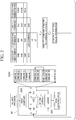
- Fig. 2 is a diagram illustrating the functions of a program generation unit according to the first embodiment.
- the first compiler 101 generates a command sequence SQC that can be processed by the system unit 30 as an object OJT.
- the command A, the command B, the command C, ..., the command XX in the command sequence SQC are each classified as one of a fixed point number command, a logic operation command, a shift operation command, a floating point number command, and an LDST command (load-and-store command).
- the second compiler 102 analyzes the command densities in the command sequence SQC as indicated below, and prepares voltage value information VIF as indicated below.
- the command densities indicate, for example, the proportions, within the command sequence SQC, occupied by the command types to which the commands included in the command sequence SQC belong.
- the second compiler 102 classifies each of the commands, i.e., the command A, the command B, the command C, ..., the command XX in the command sequence SQC, into one of the command types among fixed point number commands, logic operation commands, shift operation commands, floating point number commands, and LDST commands (load-and-store commands).
- the second compiler 102 determines the command type, among the multiple command types, into which the highest proportion of the commands included in the command sequence SQC have been classified.
- the voltage value information VIF is information for making the LSI run with operating voltage values based on voltage contexts.
- the second compiler 102 generates voltage value information VIF by performing one of the actions in the following (Case 1) to (Case 5) in accordance with the results of command density analysis, and sends the generated voltage value information VIF to the linker 103.
- the second compiler 102 classifies the commands included in the command sequence SQC into multiple command types, and generates voltage value information VIF based on the command type into which the highest proportion have been classified.
- the second compiler sets the voltage value information in accordance with the command type with the highest proportion indicated by the command density.
- the second compiler for example, sets the voltage value information to a value that is increased or decreased in accordance with the command type with the highest proportion.
- Fig. 3 is a time chart showing the operations in the information processing device according to the first embodiment.
- the execution time of each JOB is set to be short for the purpose of explanation, but the actual JOB execution times are longer than those indicated.
- Fig. 3 indicates the conditions under which the respective user programs PGM assigned to the respective cores are executed by the OS dispatcher 201.
- the respective user programs PGM that are executed are indicated as JOB01, JOB02, JOB03, JOB11, ..., JOB34.
- the OS dispatcher 201 assigns JOB01 to the first core 309A, JOB 11 to the second core 309B, JOB21 to the third core 309C, and JOB31 to the fourth core 309D.
- the voltage value transmission unit 202 generates, as the first core set voltage value Vs1, a voltage value appropriate for the first core 309A based on the voltage value information VIF.
- the voltage value transmission unit 202 sets a prescribed initial setting voltage value, unchanged, as the first core set voltage value Vs1.
- the voltage value transmission unit 202 sets a voltage value obtained by lowering the initial setting voltage value with respect to the prescribed initial setting voltage value as a new first core set voltage value Vs1.
- the voltage value transmission unit 202 sets a voltage value based on the voltage value information VIF as the new first core set voltage value Vs1.
- the voltage value transmission unit 202 generates a voltage value appropriate for the second core 309B based on the voltage value information VIF as the second core set voltage value Vs2, a voltage value appropriate for the third core 309C based on the voltage value information VIF as the third core set voltage value Vs3, and a voltage value appropriate for the fourth core 309D based on the voltage value information VIF as the fourth core set voltage value Vs4.
- the voltage value transmission unit 202 sends, to the voltage control circuit 301, the first core set voltage value Vs1, the second core set voltage value Vs2, the third core set voltage value Vs3, and the fourth core set voltage value Vs4 that have been generated.
- the voltage control circuit 301 Upon receiving the respective set voltage values form the voltage value transmission unit 202, the voltage control circuit 301 controls the operating voltage values of the respective cores so as to be the set voltage values at timing 0.
- the voltage control circuit 301 controls the first core power source 303A so that the first core operating voltage value Vc1 supplied to the first core 309A becomes the first core set voltage value Vs1.
- the voltage control circuit 301 controls the second core power source 303B so that the second core operating voltage value Vc2 supplied to the second core 309B becomes the second core set voltage value Vs2.
- the voltage control circuit 301 controls the third core power source 303C so that the third core operating voltage value Vc3 supplied to the third core 309C becomes the third core set voltage value Vs3.
- the voltage control circuit 301 controls the fourth core power source 303D so that the fourth core operating voltage value Vc4 supplied to the fourth core 309D becomes the fourth core set voltage value Vs4.
- the information processing device 1 similarly sets the host interface operating voltage value Vci.
- the voltage value transmission unit 202 generates, as the host interface set voltage value Vsi, a voltage value that is appropriate for the host interface 306 based on the voltage information VIF, and sends the generated host interface set voltage value Vsi to the voltage control circuit 301. Furthermore, the voltage control circuit 301 controls the IO power source 303F so that the host interface operating voltage value Vci supplied to the host interface 306 becomes the host interface set voltage value Vsi.
- the voltage value transmission unit 202 sets, as a new host interface set voltage value Vsi, a voltage value obtained by raising the voltage of the initial setting with respect to the prescribed initial setting voltage value.
- the voltage control circuit 301 controls the memory control operating voltage value Vcm so as to become a prescribed initial setting voltage value.
- the voltage value transmission unit 202 generates, as the first core set voltage value Vs1, a voltage value appropriate for the first core 309A based on the voltage value information VIF.
- the information processing device 1 lowers the voltage supplied to the first core 309A one timing before the timing at which the execution of JOB02 is started.
- the voltage value transmission unit 202 For example, if the voltage value information VIF for JOB02 is "settings information for lowering the core operating voltage value", then the voltage value transmission unit 202 generates, as a new first core set voltage value Vs1, a voltage lower than the first core set voltage value Vs1 that was set at timing 1, and sends the new first core set voltage value Vs1 to the voltage control circuit 301. As a result thereof, the information processing device 1 lowers the voltage supplied to the first core 309A one timing before the timing at which the execution of JOB02 is started.
- the voltage value transmission unit 202 generates, as the first core set voltage value Vs1, a voltage value appropriate for the first core 309A based on the voltage value information VIF.
- the information processing device 1 raises the voltage supplied to the first core 309A one timing before the timing at which the execution of JOB03 is started.
- the execution of JOB12 is started at timing 10
- the execution of JOB13 is started at timing 18 in the second core 309B.
- the voltage value transmission unit 202 respectively generates, as new second core set voltage values Vs2, voltage values appropriate for the second core 309B based on the voltage value information VIF.
- the execution of JOB22 is started at timing 7, and the execution of JOB23 is started at timing 13 in the third core 309C.
- the voltage value transmission unit 202 respectively generates, as new third core set voltage values Vs3, voltage values appropriate for the third core 309C based on the voltage value information VIF.
- the appropriate voltage value is the same for JOB22 and JOB23.
- the third core set voltage value Vs3 generated for JOB22 and the third core set voltage value Vs3 generated for JOB23 are the same voltage.
- the execution of JOB32 is started at timing 7
- the execution of JOB33 is started at timing 12
- the execution of JOB34 is started at timing 17 in the fourth core 309D.
- the voltage value transmission unit 202 respectively generates, as new fourth core set voltage values Vs4, voltage values appropriate for the fourth core 309D based on the voltage value information VIF.
- the appropriate voltage value is the same for JOB33 and JOB34.
- the fourth core set voltage value Vs4 generated for JOB33 and the fourth core set voltage value Vs4 generated for JOB34 are the same voltage.
- the second compiler 102 analyzes the respective command densities of fixed point number commands, LDST commands, logic operation commands, shift operation commands, and floating point number commands in a command sequence. For this reason, voltages appropriate for the respective user programs PGM can be supplied to the cores and the host interface without checking for the operating voltage values that are appropriate for the respective user programs PGM in advance. Thus, it is possible to eliminate wasted power consumption.
- the necessary voltage values are supplied for the respective user programs PGM.
- the information processing device 1 can suppress wasted power and achieve low power consumption.
- the power sources of the respective cores are separated, and the operating voltage values can be controlled separately for the respective cores and the host interface.
- the information processing device 1 can supply power separately to each core and the host interface by setting, separately for each core and the host interface, voltages appropriate for the assigned user programs PGM.
- the information processing device 1 can supply the optimum power with less waste.
- Voltage values are set so as to allow operation even for programs in which the maximum electric current flows. For this reason, in an information processing device in which the operating voltage values are not changed, excessive power is sometimes supplied depending on the program.
- the information processing device 1 of the present embodiment analyzes the command densities of command sequences. Thus, there is no need to check for the operating voltage values appropriate for the respective user programs PGM in advance.
- the operating voltage values appropriate for executing the user programs PGM can be supplied to the cores from the first time the user programs PGM are executed. Furthermore, even if a user program PGM is updated, appropriate operating voltage values can be supplied to the cores.
- the operating voltage values are changed in accordance with a command sequence in order to reduce excess power.
- an operating voltage value control command is added to the front of consecutive commands to issue an operating voltage value change instruction.
- the information processing device 1 in the present embodiment changes the voltages supplied to the respective cores during CSW times before the execution of the respective user programs PGM.
- the information processing device 1 in the present embodiment can suppress the occurrence of time lag in the voltage change such as that in Patent Document 2.
- the information processing device 1' according to the present embodiment differs in that a power source is shared by the cores. Aside from the points explained below, the structure of the information processing device 1' is similar to that of the information processing device 1 according to the first embodiment.
- the information processing device 1' is provided with a program generation unit 10, a host unit 20', and a system unit 30'.
- the host unit 20' is provided with an OS dispatcher 201 and a voltage value transmission unit 202'.
- the system unit 30' is provided with a voltage control circuit 301', a memory unit 307, and an LSI 309'.
- the system unit 30' is further provided with an internal power source 303A' and an IO power source 303F.
- these power sources are DC/DC converters, and the output voltages are controlled by control from the voltage control circuit 301'.
- the voltage value transmission unit 202' sequentially receives the voltage value information VIF of the respective user programs PGM from the OS dispatcher 201.
- the voltage value transmission unit 202' generates set voltage values based on the voltage value information VIF of the respective user programs PGM, and sends the set voltage values to the voltage control circuit 301'.
- the system unit 30' sets the operating voltage values in the respective cores to the set voltage values transmitted from the voltage value transmission unit 202'.
- the voltage control circuit 301' receives the set voltage values from the voltage value transmission unit 202'.
- the voltage control circuit 301' respectively controls the output voltages from the internal power source 303A' and the IO power source 303F based on the set voltage values that have been received.
- the internal power source 303A' is a power source that is common to the first core 309A, the second core 309B, the third core 309C, the fourth core 309D, and the memory control unit 310.
- the internal power source 303A' outputs a common operating voltage Vcc, which is a prescribed DC voltage, in accordance with control by the voltage control circuit 301', and supplies power to the first core 309A, the second core 309B, the third core 309C, the fourth core 309D, and the memory control unit 310.
- Vcc a common operating voltage
- Fig. 5 is a time chart of the operations in the information processing device according to the second embodiment. As illustrated in Fig. 5 , first, at timing 0, a first core set voltage value Vs1, a second core set voltage value Vs2, a third core set voltage value Vs3, and a fourth core set voltage value Vs4 are generated.
- the generated first core set voltage value Vs1, the second core set voltage value Vs2, the third core set voltage value Vs3, and the fourth core set voltage value Vs4 are summed to compute a common set voltage value Vsc.
- the voltage value transmission unit 202' sends the generated common set voltage value Vsc to the voltage control circuit 301'.
- the voltage control circuit 301' upon receiving the common set voltage value Vsc from the voltage value transmission unit 202', controls the internal power source 303A' so that the common operating voltage value Vcc becomes the common set voltage value Vsc at timing 0.
- the information processing device 1' similarly sets the host interface operating voltage value Vci, separately from the common operating voltage value Vcc.
- the voltage value transmission unit 202' generates, as the host interface set voltage value Vsi, a voltage value appropriate for the host interface 306 based on the voltage value information VIF, and sends the generated host interface set voltage value Vsi to the voltage control circuit 301'. Furthermore, the voltage control circuit 301' controls the IO power source 303F so that the host interface operating voltage value Vci supplied to the host interface 306 becomes the host interface set voltage value Vsi.
- the voltage value transmission unit 202' computes the common set voltage value Vsc before the respective user programs PGM are executed (CSW times before the execution of the user programs PGM).
- the voltage value transmission unit 202' computes the common set voltage value Vsc by summing the respective set voltage values of the four cores, namely, the first core set voltage value Vs1, the second core set voltage value Vs2, the third core set voltage value Vs3, and the fourth core set voltage value Vs4, at each timing.
- the voltage value transmission unit 202' counts the number of instructions for lowering the set voltage value (voltage value lowering instruction number), as indicated in Fig. 5 .
- the voltage value transmission unit 202' generates, as the new common set voltage value Vsc, a voltage lower than the common set voltage value Vsc that was set, and sends the new common set voltage value Vsc to the voltage control circuit 301'.
- the voltage control circuit 301' Upon receiving the new common set voltage value Vsc from the voltage value transmission unit 202', the voltage control circuit 301' controls the internal power source 303A' so that the common operating voltage value Vcc becomes the new common set voltage value Vsc, before the respective user programs are executed (CSW times before the execution of the user programs PGM).
- the original common operating voltage value Vcc is set so as to be able to operate even with a user program PGM in which the maximum electric current flows. For this reason, if the common operating voltage value Vcc is lowered on the basis of the criterion "voltage value lowering instruction number of four cores ⁇ 3", then the user programs PGM can be executed without hindering the operation of the user programs PGM.
- the voltage value lowering instruction number shifts to become three or higher.
- the voltage value transmission unit 202' generates a lower voltage as a new common set voltage value Vsc.
- the voltage control circuit 301' controls the internal power source 303' so that the common set voltage value Vcc becomes the new common set voltage value Vsc.
- the information processing device 1' lowers the voltage supplied to the respective cores and the memory control unit 310 one timing before the timing at which the execution of JOB02 is started.
- the information processing device 1' makes the common operating voltage value Vcc higher, as indicated at timing 15 in Fig. 5 .
- the voltage value lowering instruction number shifts to become less than three at timing 14. For this reason, the voltage value transmission unit 202' generates a higher voltage as a new common set voltage value Vsc.
- the voltage control circuit 301' controls the internal power source 303A' so that the common operating voltage value Vcc becomes the new common set voltage value Vsc, as indicated at timing 15. As a result thereof, the information processing device 1' raises the voltage supplied to the respective cores and the memory control unit 310 one timing before the timing at which the execution of JOB03 is started.
- the voltage value transmission unit 202' changes the common set voltage value Vsc when the voltage value lowering instruction number shifts to become three or higher, or when the voltage value lowering instruction number shifts to become less than three.
- the voltage value transmission unit 202' may, for example, change the common set voltage value Vsc when the voltage value lowering instruction number shifts to become two or higher, or when the voltage value lowering instruction number shifts to become less than two.
- the voltage value transmission unit 202' may recompute the common set voltage value Vsc by summing the set voltage values of the respective cores.
- the second compiler 102 analyzes the respective command densities of fixed point number commands, LDST commands, logic operation commands, shift operation commands, and floating point number commands in a command sequence. For this reason, voltages appropriate for the respective user programs PGM can be supplied to the respective cores and the host interface without checking for the operating voltage values that are appropriate for the respective user programs in advance. Thus, it becomes possible to eliminate wasted power consumption.
- the common operating voltage value is changed during CSW times before the execution of the respective user programs PGM.
- the internal power source 303A' is a power source that is common to the first core 309A, the second core 309B, the third core 309C, the fourth core 309D, and the memory control unit 310.
- the number of power sources to be mounted can be suppressed relative to the information processing device 1 in the first embodiment.
- the cost can be suppressed and the size of the information processing device 1' can be made smaller.
- Fig. 6 is a flow chart of the program generation method according to the embodiments.
- the present program generation method generates user programs PGM to be executed by an LSI at operating voltage values based on voltage information VIF.
- the program generation unit 10 compiles a source program prepared by a user, and generates an object including a command sequence (ST10: step of generating obj ect).
- the program generation unit 10 analyzes the command densities in the command sequence and generates voltage value information (ST20: step of generating voltage value information).
- the program generation unit 10 links the object OJT with the voltage value information VIF, and generates user programs PGM (ST30: step of generating programs).
- Fig. 7 illustrates an example of a hardware structure for realizing the program generation unit 10 in the above-mentioned embodiments.
- the program generation unit 10 is a computer provided with hardware including a CPU (Central Processing Unit) 105, a memory unit 106, a storage/playback device 107, a HDD (Hard Disk Drive) 108, an IO interface (Input Output Interface) 109, and the like.
- a CPU Central Processing Unit
- memory unit 106 a memory unit 106
- HDD Hard Disk Drive
- IO interface Input Output Interface
- the memory unit 106 is a storage medium such as a RAM (Random Access Memory) or a ROM (Read Only Memory).
- the storage/playback device 107 is a device for storing programs, data, and the like in external media such as a CD-ROM, a DVD, or a flash memory, and for playing programs, data, and the like in the external media.
- the IO interface 109 is an interface for inputting source programs, and for inputting and outputting information and the like with respect to the host unit 20 (20').
- the processes in the respective units may be performed by storing a program for realizing all or some of the functions of the program generation unit on a computer-readable storage medium, reading the program stored on this recording medium into a computer system, and executing the program.
- the "computer system” mentioned here includes hardware such as an OS and peripheral devices.
- the "computer system” includes homepage-providing environments (or display environments) in the case in which a WWW system is used.
- “computer-readable recording medium” refers to portable media such as flexible disks, magneto-optic disks, ROMs, and CD-ROMs, and also to storage apparatus, such as hard disks, installed internally in a computer system.
- the "computer-readable recording medium” may include those that dynamically hold the program for a short time, such as communication cables when the program is transmitted over a network such as the internet or over a communication line such as a telephone line, and in this case, may include those that hold the program for a certain period of time, such as volatile memory inside a computer system used as a server or a client.
- the above-mentioned program may be for the purpose of realizing some of the aforementioned functions, and furthermore, the aforementioned functions may be able to be realized by being combined with a program that is already stored in the computer system.
- Fig. 8 illustrates the minimum structure of the program generation unit 10 in the above-mentioned embodiments.
- the program generation unit 10 generates voltage value information for making an LSI run on operating voltage values based on voltage contexts.
- the program generation unit 10 is provided with a first compiler 101, a second compiler 102, and a linker 103.
- the first compiler 10 compiles a source program and generates an object including a command sequence.
- the second compiler 102 analyzes the command densities in the command sequence and generates voltage value information.
- the linker 103 links the object with voltage value information and generates user programs.
- the LSI is composed of four cores, but it may be composed of any number of cores. As a modified example, it may be composed of five or more cores. As another modified example, it may be composed of three or fewer cores.
- the second compiler 102 classifies the commands included in the command sequence into command types including LDST commands, logic operation commands, shift operation commands, fixed point number commands, and floating point number commands.
- the second compiler 102 may classify the respective commands included in the command sequence into at least two or more command types among LDST commands, logic operation commands, shift operation commands, fixed point number commands, and floating point number commands.
- the command types may include command types other than LDST commands, logic operation commands, shift operation commands, fixed point number commands, and floating point number commands.
- the information processing device controls the memory control operating voltage value Vcm so as to be a prescribed initial setting voltage value.
- the information processing device may generate a memory control set voltage value appropriate for the memory control unit based on voltage value information VIF, and may control the memory control operating voltage value Vcm so as to be a memory control set voltage value.
- the respective set voltage values of the four cores are summed to compute the common set voltage value Vsc.
- the host interface set voltage value Vsi may be summed together with the respective set voltage values of the four cores.
- changing operating voltage values in accordance with user programs does not tend to create a burden.
Landscapes
- Engineering & Computer Science (AREA)
- Theoretical Computer Science (AREA)
- General Engineering & Computer Science (AREA)
- Physics & Mathematics (AREA)
- General Physics & Mathematics (AREA)
- Software Systems (AREA)
- Power Sources (AREA)
- Devices For Executing Special Programs (AREA)
Abstract
Description
- The present invention relates to a program generation unit, an information processing device, a program generation method, and a program.
- The controlling of information processing devices so as to eliminate power consumption is known.
- For example,
Patent Document 1 andPatent Document 2 disclose the feature of changing operating voltage values in order to control the power consumption so as to be reduced. -
- [Patent Document 1]
Japanese Unexamined Patent Application, First Publication No.2010-250858 - [Patent Document 2]
Japanese Unexamined Patent Application, First Publication No.2003-202942 -
Patent Document 1 discloses the feature of changing operating voltage values based on power contexts in which power control information is stored for each program. - The information processing device in
Patent Document 1 changes the operating voltage values when executing programs based on success rates or failure rates in the power control information, which are power contexts. However, inPatent Document 1, in order to generate power contexts, a program must be executed at least once in order to check the success rate or the failure rate in advance, and changing the operating voltage values in accordance with user programs creates a burden. - Additionally, in
Patent Document 2, if a set of commands in which the same minimum operating voltage value command occurs consecutively is detected, then the operating voltage values are changed when a program is executed. - However, in
Patent Document 2, the operating voltage values are not changed as long as the same minimum operating voltage value command does not occur consecutively. For this reason, operating voltage values that are appropriate for programs must be checked in advance, and changing the operating voltage values in accordance with user programs creates a burden. - In view of the above-mentioned problems, an example objective of the present invention is to provide a program generation unit, an information processing device, a program generation method, and a program in which changing operating voltage values in accordance with user programs does not tend to create a burden.
- According to a first aspect of the present invention, a program generation unit generates voltage value information for making an LSI run on an operating voltage value based on a voltage context. The program generation unit includes: a first compiler configured to compile a source program and that generates an object including a command sequence; a second compiler configured to generate the voltage value information based on a command density in the command sequence; and a linker configure to link the object with the voltage value information and that generates a user program.
- According to a second aspect of the present invention, a program generation method generates voltage value information for making an LSI run on an operating voltage value based on a voltage context. The program generation method includes: compiling a source program and generating an object including a command sequence; generating the voltage value information based on a command density in the command sequence; and linking the object with the voltage value information and generating a user program.
- According to a third aspect of the present invention, a program makes a computer generate voltage value information for making an LSI run on an operating voltage value based on a voltage context, wherein the program makes the computer execute processes. The process includes: compiling a source program and generating an object including a command sequence; generating the voltage value information based on a command density in the command sequence; and linking the object with the voltage value information and generating a user program.
- According to the present invention, changing operating voltage values in accordance with user programs does not tend to create a burden.
-
-
Fig. 1 is a block diagram of an information processing device according to a first embodiment. -
Fig. 2 is a diagram illustrating the functions of a program generation unit according to a first embodiment. -
Fig. 3 is a time chart of the operations in the information processing device according to the first embodiment. -
Fig. 4 is a block diagram of an information processing device according to a second embodiment. -
Fig. 5 is a time chart of the operations in the information processing device according to the second embodiment. -
Fig. 6 is a flow chart of the program generation method according to each embodiment. -
Fig. 7 is a hardware structure diagram of the program generation unit according to each embodiment. -
Fig. 8 is a minimum structure diagram of the program generation unit according to each embodiment. - Hereinafter, various embodiments of the present invention will be explained by using the drawings.
- An information processing device according to a first embodiment will be explained with reference to
Fig. 1 to 3 . - As illustrated in
Fig. 1 , aninformation processing device 1 is provided with aprogram generation unit 10, ahost unit 20, and asystem unit 30. - The
program generation unit 10 is provided with afirst compiler 101, asecond compiler 102, and a linker 103. - The
host unit 20 is provided with anOS dispatcher 201 and a voltagevalue transmission unit 202. - The
system unit 30 is provided with avoltage control circuit 301, amemory unit 307 and anLSI 309. - The
system unit 30 is further provided with a firstcore power source 303A, a secondcore power source 303B, a thirdcore power source 303C, a fourthcore power source 303D, a memorycontrol power source 303E, and anIO power source 303F. In the present embodiment, each of these power sources is a DC/DC converter, and the output voltages are controlled by control from thevoltage control circuit 301. - The LSI 309 is provided with a
first core 309A, asecond core 309B, athird core 309C, afourth core 309D, ahost interface 306, and amemory control unit 310. - The
first compiler 101 receives a source program prepared by a user. - The
first compiler 101 compiles the received source program and generates an object OJT including a command sequence. - The
first compiler 101 sends the generated object OJT to both thesecond compiler 102 and the linker 103. - The
second compiler 102 receives the object OJT from thefirst compiler 101. - The
second compiler 102 analyzes the command densities, respectively, of fixed point number commands, LDST commands, logic operation commands, shift operation commands, and floating point number commands in the received object OJT, and generates voltage value information VIF. - The
second compiler 102 sends the generated voltage value information VIF to the linker 103. - The linker 103 receives the object OJT from the
first compiler 101. Additionally, the linker 103 receives the voltage value information VIF from thesecond compiler 102. - The linker 103 links the object OJT with the voltage value information VIF, and sequentially generates user programs PGM (programs).
- The linker 103 sequentially sends the generated user programs PGM to the
host unit 20. - The
OS dispatcher 201 sequentially receives the user programs PGM generated by the linker 103. - The
OS dispatcher 201 assigns the cores that are to execute the respective user programs PGM that have been sequentially received. TheOS dispatcher 201 considers the free space in each of the cores, namely, thefirst core 309A, thesecond core 309B, thethird core 309C, and thefourth core 309D, and determines which core to assign each user program PGM. For example, theOS dispatcher 201 determines the core that is to be assigned to each user program PGM based on the processing conditions, such as the usage state and the load state of the resources in each core. - The
OS dispatcher 201 sequentially sends the voltage value information VIF of the respective user programs PGM to the voltagevalue transmission unit 202. - The voltage
value transmission unit 202 sequentially receives the voltage value information VIF of the respective user programs PGM from theOS dispatcher 201. - The voltage
value transmission unit 202 generates set voltage values based on the voltage value information VIF of the respective user programs PGM, and sends the set voltage values to thevoltage control circuit 301. - Before the respective user programs PGM are executed, the
system unit 30 sets the operating voltage values in the cores and thehost interface 306 to the set voltage values transmitted from the voltagevalue transmission unit 202. - Hereinafter, "before the respective user programs PGM are executed" will refer to context switching (CSW) times before the user programs PGM start being executed in the respective cores. The CSW, for example, indicates steps for saving and restoring the states of the cores so that multiple processes can share a single core.
- The
voltage control circuit 301 receives the set voltage values from the voltagevalue transmission unit 202. Thevoltage control circuit 301 controls the respective output voltages from the firstcore power source 303A, the secondcore power source 303B, the thirdcore power source 303C, the fourthcore power source 303D, the memorycontrol power source 303E, and theIO power source 303F based on the set voltage values that have been received. - The first
core power source 303A supplies power to thefirst core 309A by outputting a first core operating voltage value Vc1, which is a prescribed DC voltage, in accordance with the control by thevoltage control circuit 301. - The second
core power source 303B supplies power to thesecond core 309B by outputting a second core operating voltage value Vc2, which is a prescribed DC voltage, in accordance with the control by thevoltage control circuit 301. - The third
core power source 303C supplies power to thethird core 309C by outputting a third core operating voltage value Vc3, which is a prescribed DC voltage, in accordance with the control by thevoltage control circuit 301. - The fourth
core power source 303D supplies power to thefourth core 309D by outputting a fourth core operating voltage value Vc4, which is a prescribed DC voltage, in accordance with the control by thevoltage control circuit 301. - The memory
control power source 303E supplies power to thememory control unit 310 by outputting a memory control operating voltage value Vcm, which is a prescribed DC voltage, in accordance with the control by thevoltage control circuit 301. - The
IO power source 303F supplies power to thehost interface 306 by outputting an IO operating voltage value Vci, which is a prescribed DC voltage, in accordance with the control by thevoltage control circuit 301. - The
memory unit 307 is a common memory unit that can be accessed by any of the cores for reading and writing data. - The
first core 309A, thesecond core 309B, thethird core 309C, and thefourth core 309D each process user programs PGM assigned by theOS dispatcher 201. - The
host interface 306 communicates with theOS dispatcher 201 and supplies the user programs PGM to the cores, among the respective cores, to which the user programs PGM have been assigned. - The
memory control unit 310 controls access to thememory unit 307 by each of the cores among thefirst core 309A, thesecond core 309B, thethird core 309C, and thefourth core 309D. - The functions of the
first compiler 101 and thesecond compiler 102 will be explained in detail. -
Fig. 2 is a diagram illustrating the functions of a program generation unit according to the first embodiment. Thefirst compiler 101 generates a command sequence SQC that can be processed by thesystem unit 30 as an object OJT. - In the case of the present embodiment, as illustrated in
Fig. 2 , the command A, the command B, the command C, ..., the command XX in the command sequence SQC are each classified as one of a fixed point number command, a logic operation command, a shift operation command, a floating point number command, and an LDST command (load-and-store command). - The
second compiler 102 analyzes the command densities in the command sequence SQC as indicated below, and prepares voltage value information VIF as indicated below. The command densities indicate, for example, the proportions, within the command sequence SQC, occupied by the command types to which the commands included in the command sequence SQC belong. - The
second compiler 102 classifies each of the commands, i.e., the command A, the command B, the command C, ..., the command XX in the command sequence SQC, into one of the command types among fixed point number commands, logic operation commands, shift operation commands, floating point number commands, and LDST commands (load-and-store commands). - As a result of the command density analysis, the
second compiler 102 determines the command type, among the multiple command types, into which the highest proportion of the commands included in the command sequence SQC have been classified. - The voltage value information VIF is information for making the LSI run with operating voltage values based on voltage contexts.
- The
second compiler 102 generates voltage value information VIF by performing one of the actions in the following (Case 1) to (Case 5) in accordance with the results of command density analysis, and sends the generated voltage value information VIF to thelinker 103. In other words, thesecond compiler 102 classifies the commands included in the command sequence SQC into multiple command types, and generates voltage value information VIF based on the command type into which the highest proportion have been classified. - (Case 1) If the proportion of LDST commands is the highest, then "settings information for raising the IO operating voltage value" is generated as the voltage value information VIF.
- (Case 2) If the proportion of logic operation commands is the highest, then "settings information for lowering the core operating voltage values" is generated as the voltage value information VIF.
- (Case 3) If the proportion of shift operation commands is the highest, then "settings information for setting the core operating voltage values to an intermediate voltage" is generated as the voltage value information VIF.
- (Case 4) If the proportion of fixed point number commands is the highest, then "settings information for setting the core operating voltage values to an intermediate voltage" is generated as the voltage value information VIF.
- (Case 5) If the proportion of floating point number commands is the highest, then "settings information for setting the core operating voltage values to the maximum" is generated as the voltage value information VIF.
- Thus, the second compiler sets the voltage value information in accordance with the command type with the highest proportion indicated by the command density. The second compiler, for example, sets the voltage value information to a value that is increased or decreased in accordance with the command type with the highest proportion.
- The functions of the voltage
value transmission unit 202 will be explained in detail. -
Fig. 3 is a time chart showing the operations in the information processing device according to the first embodiment. InFig. 3 , the execution time of each JOB is set to be short for the purpose of explanation, but the actual JOB execution times are longer than those indicated.Fig. 3 indicates the conditions under which the respective user programs PGM assigned to the respective cores are executed by theOS dispatcher 201. InFig. 3 , the respective user programs PGM that are executed are indicated as JOB01, JOB02, JOB03, JOB11, ..., JOB34. - First, at
timing 0, theOS dispatcher 201 assigns JOB01 to thefirst core 309A,JOB 11 to thesecond core 309B, JOB21 to thethird core 309C, and JOB31 to thefourth core 309D. - In this case, at
timing 0, the voltagevalue transmission unit 202 generates, as the first core set voltage value Vs1, a voltage value appropriate for thefirst core 309A based on the voltage value information VIF. - In (Case 1), the voltage
value transmission unit 202 sets a prescribed initial setting voltage value, unchanged, as the first core set voltage value Vs1. - In (Case 2), the voltage
value transmission unit 202 sets a voltage value obtained by lowering the initial setting voltage value with respect to the prescribed initial setting voltage value as a new first core set voltage value Vs1. - In (
Cases 3 to 5), the voltagevalue transmission unit 202 sets a voltage value based on the voltage value information VIF as the new first core set voltage value Vs1. - Similarly, at
timing 0, the voltagevalue transmission unit 202 generates a voltage value appropriate for thesecond core 309B based on the voltage value information VIF as the second core set voltage value Vs2, a voltage value appropriate for thethird core 309C based on the voltage value information VIF as the third core set voltage value Vs3, and a voltage value appropriate for thefourth core 309D based on the voltage value information VIF as the fourth core set voltage value Vs4. - In the present embodiment, at
timing 0, the voltagevalue transmission unit 202 sends, to thevoltage control circuit 301, the first core set voltage value Vs1, the second core set voltage value Vs2, the third core set voltage value Vs3, and the fourth core set voltage value Vs4 that have been generated. - Upon receiving the respective set voltage values form the voltage
value transmission unit 202, thevoltage control circuit 301 controls the operating voltage values of the respective cores so as to be the set voltage values attiming 0. - Specifically, the
voltage control circuit 301 controls the firstcore power source 303A so that the first core operating voltage value Vc1 supplied to thefirst core 309A becomes the first core set voltage value Vs1. - Similarly, the
voltage control circuit 301 controls the secondcore power source 303B so that the second core operating voltage value Vc2 supplied to thesecond core 309B becomes the second core set voltage value Vs2. - Similarly, the
voltage control circuit 301 controls the thirdcore power source 303C so that the third core operating voltage value Vc3 supplied to thethird core 309C becomes the third core set voltage value Vs3. - Similarly, the
voltage control circuit 301 controls the fourthcore power source 303D so that the fourth core operating voltage value Vc4 supplied to thefourth core 309D becomes the fourth core set voltage value Vs4. - Though not shown in
Fig. 3 , theinformation processing device 1 similarly sets the host interface operating voltage value Vci. - In other words, at
timing 0, the voltagevalue transmission unit 202 generates, as the host interface set voltage value Vsi, a voltage value that is appropriate for thehost interface 306 based on the voltage information VIF, and sends the generated host interface set voltage value Vsi to thevoltage control circuit 301. Furthermore, thevoltage control circuit 301 controls theIO power source 303F so that the host interface operating voltage value Vci supplied to thehost interface 306 becomes the host interface set voltage value Vsi. - In
Case 1, the voltagevalue transmission unit 202 sets, as a new host interface set voltage value Vsi, a voltage value obtained by raising the voltage of the initial setting with respect to the prescribed initial setting voltage value. - Additionally, in the present embodiment, the
voltage control circuit 301 controls the memory control operating voltage value Vcm so as to become a prescribed initial setting voltage value. - Next, at
timing 1, the execution, respectively, of JOB01 in thefirst core 309A, JOB11 in thesecond core 309B, JOB21 in thethird core 309C, and JOB31 in thefourth core 309D is started. - Next, at
timing 8, the execution of JOB02 is started in thefirst core 309A. At this time, one timing before the timing at which the execution of JOB02 is started, the voltagevalue transmission unit 202 generates, as the first core set voltage value Vs1, a voltage value appropriate for thefirst core 309A based on the voltage value information VIF. - In the present embodiment, the
information processing device 1 lowers the voltage supplied to thefirst core 309A one timing before the timing at which the execution of JOB02 is started. - For example, if the voltage value information VIF for JOB02 is "settings information for lowering the core operating voltage value", then the voltage
value transmission unit 202 generates, as a new first core set voltage value Vs1, a voltage lower than the first core set voltage value Vs1 that was set attiming 1, and sends the new first core set voltage value Vs1 to thevoltage control circuit 301. As a result thereof, theinformation processing device 1 lowers the voltage supplied to thefirst core 309A one timing before the timing at which the execution of JOB02 is started. - Similarly, at timing 15, the execution of JOB03 is started in the
first core 309A. At this time, one timing before the timing at which the execution of JOB3 is started, the voltagevalue transmission unit 202 generates, as the first core set voltage value Vs1, a voltage value appropriate for thefirst core 309A based on the voltage value information VIF. - In the present embodiment, the
information processing device 1 raises the voltage supplied to thefirst core 309A one timing before the timing at which the execution of JOB03 is started. - Similarly, the execution of JOB12 is started at timing 10, and the execution of JOB13 is started at timing 18 in the
second core 309B. At this time, one timing before the timing at which the execution of each JOB is started, the voltagevalue transmission unit 202 respectively generates, as new second core set voltage values Vs2, voltage values appropriate for thesecond core 309B based on the voltage value information VIF. - Similarly, the execution of JOB22 is started at
timing 7, and the execution of JOB23 is started at timing 13 in thethird core 309C. At this time, one timing before the timing at which the execution of each JOB is started, the voltagevalue transmission unit 202 respectively generates, as new third core set voltage values Vs3, voltage values appropriate for thethird core 309C based on the voltage value information VIF. - However, in the case of the present embodiment, the appropriate voltage value is the same for JOB22 and JOB23. For this reason, the third core set voltage value Vs3 generated for JOB22 and the third core set voltage value Vs3 generated for JOB23 are the same voltage.
- Similarly, the execution of JOB32 is started at
timing 7, the execution of JOB33 is started at timing 12, and the execution of JOB34 is started at timing 17 in thefourth core 309D. At this time, one timing before the timing at which the execution of each JOB is started, the voltagevalue transmission unit 202 respectively generates, as new fourth core set voltage values Vs4, voltage values appropriate for thefourth core 309D based on the voltage value information VIF. - However, in the case of the present embodiment, the appropriate voltage value is the same for JOB33 and JOB34. For this reason, the fourth core set voltage value Vs4 generated for JOB33 and the fourth core set voltage value Vs4 generated for JOB34 are the same voltage.
- In the
information processing device 1 of the present embodiment, thesecond compiler 102 analyzes the respective command densities of fixed point number commands, LDST commands, logic operation commands, shift operation commands, and floating point number commands in a command sequence. For this reason, voltages appropriate for the respective user programs PGM can be supplied to the cores and the host interface without checking for the operating voltage values that are appropriate for the respective user programs PGM in advance. Thus, it is possible to eliminate wasted power consumption. - Therefore, in the
information processing device 1, changes to the operating voltage values in accordance with the respective user programs PGM do not tend to become a burden. - Additionally, in the present embodiment, the necessary voltage values are supplied for the respective user programs PGM. Thus, the
information processing device 1 can suppress wasted power and achieve low power consumption. - Furthermore, in the present embodiment, the power sources of the respective cores are separated, and the operating voltage values can be controlled separately for the respective cores and the host interface. For this reason, the
information processing device 1 can supply power separately to each core and the host interface by setting, separately for each core and the host interface, voltages appropriate for the assigned user programs PGM. - Therefore, the
information processing device 1 can supply the optimum power with less waste. - Voltage values are set so as to allow operation even for programs in which the maximum electric current flows. For this reason, in an information processing device in which the operating voltage values are not changed, excessive power is sometimes supplied depending on the program.
- In order to reduce such excess power in the information processing device of
Patent Document 1, power control information that is separate for each program is used, and voltage control is implemented after running the program once in order to check whether or not it can be successfully run. For this reason, an information processing device as inPatent Document 1 cannot supply the cores with the appropriate operating voltage values for executing a program from the first time the program is run. Furthermore, when a program is updated, the appropriate operating voltage values cannot be supplied to the cores. - In contrast therewith, the
information processing device 1 of the present embodiment, as mentioned above, analyzes the command densities of command sequences. Thus, there is no need to check for the operating voltage values appropriate for the respective user programs PGM in advance. - Therefore, the operating voltage values appropriate for executing the user programs PGM can be supplied to the cores from the first time the user programs PGM are executed. Furthermore, even if a user program PGM is updated, appropriate operating voltage values can be supplied to the cores.
- Additionally, in the information processing device in
Patent Document 2 also, the operating voltage values are changed in accordance with a command sequence in order to reduce excess power. In the information processing device inPatent Document 2, in a command sequence, an operating voltage value control command is added to the front of consecutive commands to issue an operating voltage value change instruction. Normally, when performing voltage control, there is a time lag between the time at which the operating voltage value change instruction is issued and the time at which the operating voltage values are actually changed. For this reason, in the information processing device inPatent Document 2, there is a time lag between the time at which an operating voltage value change instruction is issued and the time at which the operating voltage values of the cores are actually changed. - In contrast therewith, the
information processing device 1 in the present embodiment changes the voltages supplied to the respective cores during CSW times before the execution of the respective user programs PGM. - Therefore, the
information processing device 1 in the present embodiment can suppress the occurrence of time lag in the voltage change such as that inPatent Document 2. - An information processing device according to a second embodiment will be explained with reference to
Fig. 4 and5 . - The information processing device 1' according to the present embodiment differs in that a power source is shared by the cores. Aside from the points explained below, the structure of the information processing device 1' is similar to that of the
information processing device 1 according to the first embodiment. - As illustrated in
Fig. 4 , the information processing device 1' is provided with aprogram generation unit 10, a host unit 20', and a system unit 30'. - The host unit 20' is provided with an
OS dispatcher 201 and a voltage value transmission unit 202'. - The system unit 30' is provided with a voltage control circuit 301', a
memory unit 307, and an LSI 309'. - The system unit 30' is further provided with an
internal power source 303A' and anIO power source 303F. In the present embodiment, these power sources are DC/DC converters, and the output voltages are controlled by control from the voltage control circuit 301'. - The voltage value transmission unit 202' sequentially receives the voltage value information VIF of the respective user programs PGM from the
OS dispatcher 201. - The voltage value transmission unit 202' generates set voltage values based on the voltage value information VIF of the respective user programs PGM, and sends the set voltage values to the voltage control circuit 301'.
- Before the respective user programs PGM are executed, the system unit 30' sets the operating voltage values in the respective cores to the set voltage values transmitted from the voltage value transmission unit 202'.
- The voltage control circuit 301' receives the set voltage values from the voltage value transmission unit 202'. The voltage control circuit 301' respectively controls the output voltages from the
internal power source 303A' and theIO power source 303F based on the set voltage values that have been received. - The
internal power source 303A' is a power source that is common to thefirst core 309A, thesecond core 309B, thethird core 309C, thefourth core 309D, and thememory control unit 310. - The
internal power source 303A' outputs a common operating voltage Vcc, which is a prescribed DC voltage, in accordance with control by the voltage control circuit 301', and supplies power to thefirst core 309A, thesecond core 309B, thethird core 309C, thefourth core 309D, and thememory control unit 310. - The functions of the voltage value transmission unit 202' will be explained in detail.
-
Fig. 5 is a time chart of the operations in the information processing device according to the second embodiment. As illustrated inFig. 5 , first, attiming 0, a first core set voltage value Vs1, a second core set voltage value Vs2, a third core set voltage value Vs3, and a fourth core set voltage value Vs4 are generated. - Next, at
timing 0, the generated first core set voltage value Vs1, the second core set voltage value Vs2, the third core set voltage value Vs3, and the fourth core set voltage value Vs4 are summed to compute a common set voltage value Vsc. - Next, at
timing 0, the voltage value transmission unit 202' sends the generated common set voltage value Vsc to the voltage control circuit 301'. - The voltage control circuit 301', upon receiving the common set voltage value Vsc from the voltage value transmission unit 202', controls the
internal power source 303A' so that the common operating voltage value Vcc becomes the common set voltage value Vsc attiming 0. - Though not illustrated in
Fig. 5 , the information processing device 1' similarly sets the host interface operating voltage value Vci, separately from the common operating voltage value Vcc. - In other words, at
timing 0, the voltage value transmission unit 202' generates, as the host interface set voltage value Vsi, a voltage value appropriate for thehost interface 306 based on the voltage value information VIF, and sends the generated host interface set voltage value Vsi to the voltage control circuit 301'. Furthermore, the voltage control circuit 301' controls theIO power source 303F so that the host interface operating voltage value Vci supplied to thehost interface 306 becomes the host interface set voltage value Vsi. - In the present embodiment, the voltage value transmission unit 202' computes the common set voltage value Vsc before the respective user programs PGM are executed (CSW times before the execution of the user programs PGM). The voltage value transmission unit 202' computes the common set voltage value Vsc by summing the respective set voltage values of the four cores, namely, the first core set voltage value Vs1, the second core set voltage value Vs2, the third core set voltage value Vs3, and the fourth core set voltage value Vs4, at each timing.
- Examples of summation of the set voltage values will be explained.
- First, for each of the set voltage values of the four cores, the voltage value transmission unit 202' counts the number of instructions for lowering the set voltage value (voltage value lowering instruction number), as indicated in
Fig. 5 . When there are three or more voltage value lowering instructions (voltage value lowering instruction number ≥ 3), the voltage value transmission unit 202' generates, as the new common set voltage value Vsc, a voltage lower than the common set voltage value Vsc that was set, and sends the new common set voltage value Vsc to the voltage control circuit 301'. - Upon receiving the new common set voltage value Vsc from the voltage value transmission unit 202', the voltage control circuit 301' controls the
internal power source 303A' so that the common operating voltage value Vcc becomes the new common set voltage value Vsc, before the respective user programs are executed (CSW times before the execution of the user programs PGM). - In the information processing device 1', the original common operating voltage value Vcc is set so as to be able to operate even with a user program PGM in which the maximum electric current flows. For this reason, if the common operating voltage value Vcc is lowered on the basis of the criterion "voltage value lowering instruction number of four cores ≥ 3", then the user programs PGM can be executed without hindering the operation of the user programs PGM.
- According to
Fig. 5 , attiming 7, the voltage value lowering instruction number shifts to become three or higher. For this reason, the voltage value transmission unit 202' generates a lower voltage as a new common set voltage value Vsc. As indicated attiming 8, the voltage control circuit 301' controls the internal power source 303' so that the common set voltage value Vcc becomes the new common set voltage value Vsc. As a result thereof, the information processing device 1' lowers the voltage supplied to the respective cores and thememory control unit 310 one timing before the timing at which the execution of JOB02 is started. - Conversely, when the voltage value lowering instruction number returns to being less than three (voltage value lowering instruction number < 3), the information processing device 1' makes the common operating voltage value Vcc higher, as indicated at timing 15 in
Fig. 5 . - According to
Fig. 5 , the voltage value lowering instruction number shifts to become less than three attiming 14. For this reason, the voltage value transmission unit 202' generates a higher voltage as a new common set voltage value Vsc. The voltage control circuit 301' controls theinternal power source 303A' so that the common operating voltage value Vcc becomes the new common set voltage value Vsc, as indicated attiming 15. As a result thereof, the information processing device 1' raises the voltage supplied to the respective cores and thememory control unit 310 one timing before the timing at which the execution of JOB03 is started. - In the present embodiment, the voltage value transmission unit 202' changes the common set voltage value Vsc when the voltage value lowering instruction number shifts to become three or higher, or when the voltage value lowering instruction number shifts to become less than three. However, the invention is not limited to this example. The voltage value transmission unit 202' may, for example, change the common set voltage value Vsc when the voltage value lowering instruction number shifts to become two or higher, or when the voltage value lowering instruction number shifts to become less than two. When changing the common set voltage value Vsc, the voltage value transmission unit 202' may recompute the common set voltage value Vsc by summing the set voltage values of the respective cores.
- In the information processing device 1' of the present embodiment, as in the
information processing device 1 of the first embodiment, thesecond compiler 102 analyzes the respective command densities of fixed point number commands, LDST commands, logic operation commands, shift operation commands, and floating point number commands in a command sequence. For this reason, voltages appropriate for the respective user programs PGM can be supplied to the respective cores and the host interface without checking for the operating voltage values that are appropriate for the respective user programs in advance. Thus, it becomes possible to eliminate wasted power consumption. - Therefore, in the information processing device 1', changes to the operating voltage values in accordance with the respective user programs PGM do not tend to become a burden.
- Additionally, in the information processing device 1' of the present embodiment, as in the
information processing device 1 of the first embodiment, the common operating voltage value is changed during CSW times before the execution of the respective user programs PGM. - Additionally, in the information processing device 1' of the present embodiment, the
internal power source 303A' is a power source that is common to thefirst core 309A, thesecond core 309B, thethird core 309C, thefourth core 309D, and thememory control unit 310. For this reason, according to the information processing device 1' of the present embodiment, the number of power sources to be mounted can be suppressed relative to theinformation processing device 1 in the first embodiment. Thus, for example, the cost can be suppressed and the size of the information processing device 1' can be made smaller. - The program generation method in the above-mentioned embodiments will be explained with reference to
Fig. 6 . -
Fig. 6 is a flow chart of the program generation method according to the embodiments. The present program generation method generates user programs PGM to be executed by an LSI at operating voltage values based on voltage information VIF. - First, the
program generation unit 10 compiles a source program prepared by a user, and generates an object including a command sequence (ST10: step of generating obj ect). - Following the generation of the object in ST10, the
program generation unit 10 analyzes the command densities in the command sequence and generates voltage value information (ST20: step of generating voltage value information). - Following the generation of the voltage value information in ST20, the
program generation unit 10 links the object OJT with the voltage value information VIF, and generates user programs PGM (ST30: step of generating programs). - When the generation of the voltage value information ends in ST30, the process in the
program generation unit 10 ends. Additionally, when the next source program is provided, theprogram generation unit 10 starts the process again. -
Fig. 7 illustrates an example of a hardware structure for realizing theprogram generation unit 10 in the above-mentioned embodiments. As illustrated in this diagram, theprogram generation unit 10 is a computer provided with hardware including a CPU (Central Processing Unit) 105, amemory unit 106, a storage/playback device 107, a HDD (Hard Disk Drive) 108, an IO interface (Input Output Interface) 109, and the like. - The
memory unit 106 is a storage medium such as a RAM (Random Access Memory) or a ROM (Read Only Memory). - The storage/
playback device 107 is a device for storing programs, data, and the like in external media such as a CD-ROM, a DVD, or a flash memory, and for playing programs, data, and the like in the external media. - The
IO interface 109 is an interface for inputting source programs, and for inputting and outputting information and the like with respect to the host unit 20 (20'). - In the above-mentioned embodiments, the processes in the respective units may be performed by storing a program for realizing all or some of the functions of the program generation unit on a computer-readable storage medium, reading the program stored on this recording medium into a computer system, and executing the program. The "computer system" mentioned here includes hardware such as an OS and peripheral devices.
- Additionally, the "computer system" includes homepage-providing environments (or display environments) in the case in which a WWW system is used.
- Additionally, "computer-readable recording medium" refers to portable media such as flexible disks, magneto-optic disks, ROMs, and CD-ROMs, and also to storage apparatus, such as hard disks, installed internally in a computer system. Furthermore, the "computer-readable recording medium" may include those that dynamically hold the program for a short time, such as communication cables when the program is transmitted over a network such as the internet or over a communication line such as a telephone line, and in this case, may include those that hold the program for a certain period of time, such as volatile memory inside a computer system used as a server or a client. Additionally, the above-mentioned program may be for the purpose of realizing some of the aforementioned functions, and furthermore, the aforementioned functions may be able to be realized by being combined with a program that is already stored in the computer system.
- <Minimum Structures of Embodiments>
-
Fig. 8 illustrates the minimum structure of theprogram generation unit 10 in the above-mentioned embodiments. - The
program generation unit 10 generates voltage value information for making an LSI run on operating voltage values based on voltage contexts. - The
program generation unit 10 is provided with afirst compiler 101, asecond compiler 102, and alinker 103. - The
first compiler 10 compiles a source program and generates an object including a command sequence. Thesecond compiler 102 analyzes the command densities in the command sequence and generates voltage value information. Thelinker 103 links the object with voltage value information and generates user programs. - In the above-mentioned embodiments, the LSI is composed of four cores, but it may be composed of any number of cores. As a modified example, it may be composed of five or more cores. As another modified example, it may be composed of three or fewer cores.
- In the above-mentioned embodiments, the
second compiler 102 classifies the commands included in the command sequence into command types including LDST commands, logic operation commands, shift operation commands, fixed point number commands, and floating point number commands. As a modified example, thesecond compiler 102 may classify the respective commands included in the command sequence into at least two or more command types among LDST commands, logic operation commands, shift operation commands, fixed point number commands, and floating point number commands. Additionally, the command types may include command types other than LDST commands, logic operation commands, shift operation commands, fixed point number commands, and floating point number commands. - In the above-mentioned first embodiment, the information processing device controls the memory control operating voltage value Vcm so as to be a prescribed initial setting voltage value. As a modified example, the information processing device may generate a memory control set voltage value appropriate for the memory control unit based on voltage value information VIF, and may control the memory control operating voltage value Vcm so as to be a memory control set voltage value.
- In the above-mentioned second embodiment, the respective set voltage values of the four cores are summed to compute the common set voltage value Vsc. As a modified example, the host interface set voltage value Vsi may be summed together with the respective set voltage values of the four cores.
- Although various embodiments of the present invention have been explained above, these embodiments were merely described as examples, and they are not intended to limit the scope of the invention. These embodiments may be implemented in various other forms, and various omissions, replacements and changes may be made within a range not departing from the spirit of the invention. These embodiments and modifications thereof are included in the scope and the gist of the invention, and are likewise included in the invention as recited in the claims and the range of equivalents thereof.
- Priority is claimed on Japanese Patent Application No.
2018-051582, filed March 19, 2018 - According to the present invention, changing operating voltage values in accordance with user programs does not tend to create a burden.
-
- 1
- Information processing device
- 1'
- Information processing device
- 10
- Program generation unit
- 20
- Host unit
- 20'
- Host unit
- 30
- System unit
- 30'
- System unit
- 101
- First compiler
- 102
- Second compiler
- 103
- Linker
- 106
- Memory
- 107
- Storage/playback device
- 108
- HDD
- 109
- IO interface
- 201
- OS dispatcher
- 202
- Voltage value transmission unit
- 202'
- Voltage value transmission unit
- 301
- Voltage control circuit
- 301'
- Voltage control circuit
- 303A
- First core power source
- 303A'
- Internal power source
- 303B
- Second core power source
- 303C
- Third core power source
- 303D
- Fourth core power source
- 303E
- Memory control power source
- 303F
- IO power source
- 306
- Host interface
- 307
- Memory unit
- 309
- LSI
- 309'
- LSI
- 309A
- First core
- 309B
- Second core
- 309C
- Third core
- 309D
- Fourth core
- 310
- Memory control unit
- SQC
- Command sequence
- Vc1
- First core operating voltage value
- Vc2
- Second core operating voltage value
- Vc3
- Third core operating voltage value
- Vc4
- Fourth core operating voltage value
- Vcc
- Common operating voltage value
- Vci
- Host interface operating voltage value
- Vcm
- Memory control operating voltage value
- Vs1
- First core set voltage value
- Vs2
- Second core set voltage value
- Vs3
- Third core set voltage value
- Vs4
- Fourth core set voltage value
- Vsc
- Common set voltage value
- Vsi
- Host interface set voltage value
Claims (9)
- A program generation unit that generates voltage value information for making an LSI run on an operating voltage value based on a voltage context, wherein the program generation unit comprises:a first compiler configured to compile a source program and generate an object including a command sequence;a second compiler configured to generate the voltage value information based on a command density in the command sequence; anda linker configured to link the object with the voltage value information and that generates a user program.
- The program generation unit according to claim 1, wherein the command density in the command sequence indicates a proportion, in the command sequence, of a command type to which commands included in the command sequence belong.
- The program generation unit according to claim 1 or 2, wherein the second compiler classifies commands included in the command sequence into multiple command types, and generates the voltage value information based on the command type into which the highest proportion have been classified.
- The program generation unit according to claim 2 or 3, wherein the second compiler sets voltage value information in accordance with the command type into which the highest proportion have been classified, indicated by the command density.
- The program generation unit according to any one of claims 2 to 4, wherein the second compiler classifies the command types into at least two or more of LDST commands, logic operation commands, shift operation commands, fixed point number commands, and floating point number commands.
- An information processing device comprising:the program generation unit according to any one of claims 1 to 5;a host unit having a voltage transmission unit configured to generate a voltage value based on the voltage value information; anda system unit that has a core for processing the user program, and that sets the operating voltage value in the core to the voltage value before the user program is executed.
- The information processing device according to claim 6, wherein:the system unit has a plurality of the cores; andthe voltage transmission unit generates a plurality of the voltage values corresponding to the plurality of cores, sums the plurality of voltage values that have been generated, and sets the operating voltage value corresponding to the plurality of cores to the summed voltage value.
- A program generation method that generates voltage value information for making an LSI run on an operating voltage value based on a voltage context, wherein the program generation method comprises:compiling a source program and generating an object including a command sequence;generating the voltage value information based on a command density in the command sequence; andlinking the object with the voltage value information and generating a user program.
- A program that makes a computer generate voltage value information for making an LSI run on an operating voltage value based on a voltage context, wherein the program makes the computer execute processes, the process comprising:compiling a source program and generating an object including a command sequence;generating the voltage value information based on a command density in the command sequence; andlinking the object with the voltage value information and generating a user program.
Applications Claiming Priority (2)
| Application Number | Priority Date | Filing Date | Title |
|---|---|---|---|
| JP2018051582A JP7031930B2 (en) | 2018-03-19 | 2018-03-19 | Program generator, information processing device, program generation method, and program |
| PCT/JP2019/011345 WO2019181904A1 (en) | 2018-03-19 | 2019-03-19 | Program generation unit, information processing device, program generation method, and program |
Publications (3)
| Publication Number | Publication Date |
|---|---|
| EP3770753A1 true EP3770753A1 (en) | 2021-01-27 |
| EP3770753A4 EP3770753A4 (en) | 2021-12-15 |
| EP3770753B1 EP3770753B1 (en) | 2024-10-30 |
Family
ID=67986255
Family Applications (1)
| Application Number | Title | Priority Date | Filing Date |
|---|---|---|---|
| EP19771160.9A Active EP3770753B1 (en) | 2018-03-19 | 2019-03-19 | Program generation unit, information processing device, program generation method, and program |
Country Status (4)
| Country | Link |
|---|---|
| US (1) | US11656858B2 (en) |
| EP (1) | EP3770753B1 (en) |
| JP (1) | JP7031930B2 (en) |
| WO (1) | WO2019181904A1 (en) |
Families Citing this family (1)
| Publication number | Priority date | Publication date | Assignee | Title |
|---|---|---|---|---|
| CN111338606A (en) * | 2020-02-20 | 2020-06-26 | 北京邮电大学 | An Experimental System Development Framework |
Family Cites Families (17)
| Publication number | Priority date | Publication date | Assignee | Title |
|---|---|---|---|---|
| US4393377A (en) * | 1980-08-12 | 1983-07-12 | Pitney Bowes Inc. | Circuit for controlling information on a display |
| US4570217A (en) * | 1982-03-29 | 1986-02-11 | Allen Bruce S | Man machine interface |
| KR100236876B1 (en) * | 1990-03-28 | 2000-01-15 | 가나이 쓰도무 | CMOS circuit reduces signal swing |
| US6879341B1 (en) * | 1997-07-15 | 2005-04-12 | Silverbrook Research Pty Ltd | Digital camera system containing a VLIW vector processor |
| JP2003202942A (en) | 2001-11-05 | 2003-07-18 | Matsushita Electric Ind Co Ltd | How to optimize power consumption |
| JP4044756B2 (en) * | 2001-12-11 | 2008-02-06 | 松下電器産業株式会社 | Program conversion device, program conversion method, and program for realizing the program conversion device |
| WO2003073185A2 (en) * | 2002-02-28 | 2003-09-04 | Zetacon Corporation | Predictive control system and method |
| JP4082706B2 (en) * | 2005-04-12 | 2008-04-30 | 学校法人早稲田大学 | Multiprocessor system and multigrain parallelizing compiler |
| WO2006117950A1 (en) | 2005-04-27 | 2006-11-09 | Matsushita Electric Industrial Co., Ltd. | Power controller in information processor |
| US8191052B2 (en) * | 2006-12-01 | 2012-05-29 | Murex S.A.S. | Producer graph oriented programming and execution |
| US9378181B2 (en) * | 2012-11-09 | 2016-06-28 | Intel Corporation | Scalable computing array |
| US10180828B2 (en) * | 2014-04-29 | 2019-01-15 | Significs And Elements, Llc | Systems and methods for power optimization of processors |
| US20160216969A1 (en) * | 2015-01-28 | 2016-07-28 | Qualcomm Incorporated | System and method for adaptively managing registers in an instruction processor |
| US10460057B2 (en) * | 2015-11-10 | 2019-10-29 | Wei Li | Apparatus and method for modelling a modular multilevel converter in an electronic simulator |
| US10705589B2 (en) * | 2016-06-02 | 2020-07-07 | Northwestern University | System and method for associative power and clock management with instruction governed operation for power efficient computing |
| JP6587996B2 (en) | 2016-09-28 | 2019-10-09 | 水ing株式会社 | Screw press and operating method of screw press |
| US10621116B2 (en) * | 2017-06-08 | 2020-04-14 | Western Digital Technologies, Inc. | Non-volatile storage device with adaptive data bus inversion |
-
2018
- 2018-03-19 JP JP2018051582A patent/JP7031930B2/en active Active
-
2019
- 2019-03-19 US US16/981,014 patent/US11656858B2/en active Active
- 2019-03-19 EP EP19771160.9A patent/EP3770753B1/en active Active
- 2019-03-19 WO PCT/JP2019/011345 patent/WO2019181904A1/en not_active Ceased
Also Published As
| Publication number | Publication date |
|---|---|
| US11656858B2 (en) | 2023-05-23 |
| EP3770753A4 (en) | 2021-12-15 |
| US20210019129A1 (en) | 2021-01-21 |
| JP7031930B2 (en) | 2022-03-08 |
| JP2019164527A (en) | 2019-09-26 |
| WO2019181904A1 (en) | 2019-09-26 |
| EP3770753B1 (en) | 2024-10-30 |
Similar Documents
| Publication | Publication Date | Title |
|---|---|---|
| CN101221517B (en) | Device, system and method for exchanging resources between partitions of a data processing system | |
| CN113204412A (en) | Method, electronic device, and computer storage medium for task scheduling | |
| US9716383B2 (en) | Multiple supply DVFs | |
| EP4398101A1 (en) | Task scheduling execution method, and generation method and apparatus for task scheduling execution instruction | |
| US7788672B2 (en) | System for controlling assignment of a plurality of modules of a program to available execution units based on speculative executing and granularity adjusting | |
| US8839163B2 (en) | Behavioral synthesis method, behavioral synthesis program and behavioral synthesis apparatus | |
| US20180322093A1 (en) | Method and apparatus for solving a mixed integer programming problem | |
| KR101519825B1 (en) | Data processing device and control method of the same | |
| US9734268B2 (en) | Slack redistribution for additional power recovery | |
| CN113837382B (en) | Training method and system for graph neural network | |
| EP3770753B1 (en) | Program generation unit, information processing device, program generation method, and program | |
| US8522187B2 (en) | Method and data processing system to optimize performance of an electric circuit design, data processing program and computer program product | |
| US7865896B2 (en) | Facilitating scheduling of jobs by decoupling job scheduling algorithm from recorded resource usage and allowing independent manipulation of recorded resource usage space | |
| US9208055B2 (en) | Importance-based call graph construction | |
| US20120017070A1 (en) | Compile system, compile method, and storage medium storing compile program | |
| US20090083751A1 (en) | Information processing apparatus, parallel processing optimization method, and program | |
| US20240420000A1 (en) | Quantum circuit optimization method, device, equipment and storage medium | |
| US20210117239A1 (en) | Dynamic accelerator generation and deployment | |
| EP4654089A1 (en) | Quantum circuit design support program, quantum circuit design support method, and quantum circuit design support device | |
| Chen et al. | Power-manageable scheduling technique for control dominated high-level synthesis | |
| WO2014027444A1 (en) | Scheduling device and scheduling method | |
| AU2020462915B2 (en) | Information processing system for assisting in solving allocation problems, and method | |
| CN118012563A (en) | Resource allocation method, device, medium and electronic equipment | |
| US20210208989A1 (en) | Enterprise-scale time series graphite backend infrastructure | |
| US20250086003A1 (en) | Computer-readable recording medium storing control program, system, and control method |
Legal Events
| Date | Code | Title | Description |
|---|---|---|---|
| STAA | Information on the status of an ep patent application or granted ep patent |
Free format text: STATUS: THE INTERNATIONAL PUBLICATION HAS BEEN MADE |
|
| PUAI | Public reference made under article 153(3) epc to a published international application that has entered the european phase |
Free format text: ORIGINAL CODE: 0009012 |
|
| STAA | Information on the status of an ep patent application or granted ep patent |
Free format text: STATUS: REQUEST FOR EXAMINATION WAS MADE |
|
| 17P | Request for examination filed |
Effective date: 20200923 |
|
| AK | Designated contracting states |
Kind code of ref document: A1 Designated state(s): AL AT BE BG CH CY CZ DE DK EE ES FI FR GB GR HR HU IE IS IT LI LT LU LV MC MK MT NL NO PL PT RO RS SE SI SK SM TR |
|
| AX | Request for extension of the european patent |
Extension state: BA ME |
|
| DAV | Request for validation of the european patent (deleted) | ||
| DAX | Request for extension of the european patent (deleted) | ||
| A4 | Supplementary search report drawn up and despatched |
Effective date: 20211117 |
|
| RIC1 | Information provided on ipc code assigned before grant |
Ipc: G06F 1/3296 20190101ALI20211111BHEP Ipc: G06F 8/41 20180101AFI20211111BHEP |
|
| STAA | Information on the status of an ep patent application or granted ep patent |
Free format text: STATUS: EXAMINATION IS IN PROGRESS |
|
| 17Q | First examination report despatched |
Effective date: 20230704 |
|
| GRAP | Despatch of communication of intention to grant a patent |
Free format text: ORIGINAL CODE: EPIDOSNIGR1 |
|
| STAA | Information on the status of an ep patent application or granted ep patent |
Free format text: STATUS: GRANT OF PATENT IS INTENDED |
|
| INTG | Intention to grant announced |
Effective date: 20240621 |
|
| GRAS | Grant fee paid |
Free format text: ORIGINAL CODE: EPIDOSNIGR3 |
|
| GRAA | (expected) grant |
Free format text: ORIGINAL CODE: 0009210 |
|
| STAA | Information on the status of an ep patent application or granted ep patent |
Free format text: STATUS: THE PATENT HAS BEEN GRANTED |
|
| AK | Designated contracting states |
Kind code of ref document: B1 Designated state(s): AL AT BE BG CH CY CZ DE DK EE ES FI FR GB GR HR HU IE IS IT LI LT LU LV MC MK MT NL NO PL PT RO RS SE SI SK SM TR |
|
| REG | Reference to a national code |
Ref country code: GB Ref legal event code: FG4D |
|
| REG | Reference to a national code |
Ref country code: CH Ref legal event code: EP |
|
| REG | Reference to a national code |
Ref country code: DE Ref legal event code: R096 Ref document number: 602019061167 Country of ref document: DE |
|
| REG | Reference to a national code |
Ref country code: IE Ref legal event code: FG4D |
|
| REG | Reference to a national code |
Ref country code: LT Ref legal event code: MG9D |
|
| REG | Reference to a national code |
Ref country code: NL Ref legal event code: MP Effective date: 20241030 |
|
| PG25 | Lapsed in a contracting state [announced via postgrant information from national office to epo] |
Ref country code: HR Free format text: LAPSE BECAUSE OF FAILURE TO SUBMIT A TRANSLATION OF THE DESCRIPTION OR TO PAY THE FEE WITHIN THE PRESCRIBED TIME-LIMIT Effective date: 20241030 Ref country code: IS Free format text: LAPSE BECAUSE OF FAILURE TO SUBMIT A TRANSLATION OF THE DESCRIPTION OR TO PAY THE FEE WITHIN THE PRESCRIBED TIME-LIMIT Effective date: 20250228 Ref country code: PT Free format text: LAPSE BECAUSE OF FAILURE TO SUBMIT A TRANSLATION OF THE DESCRIPTION OR TO PAY THE FEE WITHIN THE PRESCRIBED TIME-LIMIT Effective date: 20250228 |
|
| PG25 | Lapsed in a contracting state [announced via postgrant information from national office to epo] |
Ref country code: FI Free format text: LAPSE BECAUSE OF FAILURE TO SUBMIT A TRANSLATION OF THE DESCRIPTION OR TO PAY THE FEE WITHIN THE PRESCRIBED TIME-LIMIT Effective date: 20241030 Ref country code: NL Free format text: LAPSE BECAUSE OF FAILURE TO SUBMIT A TRANSLATION OF THE DESCRIPTION OR TO PAY THE FEE WITHIN THE PRESCRIBED TIME-LIMIT Effective date: 20241030 |
|
| REG | Reference to a national code |
Ref country code: AT Ref legal event code: MK05 Ref document number: 1737563 Country of ref document: AT Kind code of ref document: T Effective date: 20241030 |
|
| PG25 | Lapsed in a contracting state [announced via postgrant information from national office to epo] |
Ref country code: BG Free format text: LAPSE BECAUSE OF FAILURE TO SUBMIT A TRANSLATION OF THE DESCRIPTION OR TO PAY THE FEE WITHIN THE PRESCRIBED TIME-LIMIT Effective date: 20241030 |
|
| PG25 | Lapsed in a contracting state [announced via postgrant information from national office to epo] |
Ref country code: ES Free format text: LAPSE BECAUSE OF FAILURE TO SUBMIT A TRANSLATION OF THE DESCRIPTION OR TO PAY THE FEE WITHIN THE PRESCRIBED TIME-LIMIT Effective date: 20241030 |
|
| PG25 | Lapsed in a contracting state [announced via postgrant information from national office to epo] |
Ref country code: NO Free format text: LAPSE BECAUSE OF FAILURE TO SUBMIT A TRANSLATION OF THE DESCRIPTION OR TO PAY THE FEE WITHIN THE PRESCRIBED TIME-LIMIT Effective date: 20250130 |
|
| PG25 | Lapsed in a contracting state [announced via postgrant information from national office to epo] |
Ref country code: LV Free format text: LAPSE BECAUSE OF FAILURE TO SUBMIT A TRANSLATION OF THE DESCRIPTION OR TO PAY THE FEE WITHIN THE PRESCRIBED TIME-LIMIT Effective date: 20241030 Ref country code: GR Free format text: LAPSE BECAUSE OF FAILURE TO SUBMIT A TRANSLATION OF THE DESCRIPTION OR TO PAY THE FEE WITHIN THE PRESCRIBED TIME-LIMIT Effective date: 20250131 Ref country code: AT Free format text: LAPSE BECAUSE OF FAILURE TO SUBMIT A TRANSLATION OF THE DESCRIPTION OR TO PAY THE FEE WITHIN THE PRESCRIBED TIME-LIMIT Effective date: 20241030 |
|
| PG25 | Lapsed in a contracting state [announced via postgrant information from national office to epo] |
Ref country code: PL Free format text: LAPSE BECAUSE OF FAILURE TO SUBMIT A TRANSLATION OF THE DESCRIPTION OR TO PAY THE FEE WITHIN THE PRESCRIBED TIME-LIMIT Effective date: 20241030 |
|
| PG25 | Lapsed in a contracting state [announced via postgrant information from national office to epo] |
Ref country code: RS Free format text: LAPSE BECAUSE OF FAILURE TO SUBMIT A TRANSLATION OF THE DESCRIPTION OR TO PAY THE FEE WITHIN THE PRESCRIBED TIME-LIMIT Effective date: 20250130 |
|
| PG25 | Lapsed in a contracting state [announced via postgrant information from national office to epo] |
Ref country code: SM Free format text: LAPSE BECAUSE OF FAILURE TO SUBMIT A TRANSLATION OF THE DESCRIPTION OR TO PAY THE FEE WITHIN THE PRESCRIBED TIME-LIMIT Effective date: 20241030 |
|
| PG25 | Lapsed in a contracting state [announced via postgrant information from national office to epo] |
Ref country code: DK Free format text: LAPSE BECAUSE OF FAILURE TO SUBMIT A TRANSLATION OF THE DESCRIPTION OR TO PAY THE FEE WITHIN THE PRESCRIBED TIME-LIMIT Effective date: 20241030 |
|
| PG25 | Lapsed in a contracting state [announced via postgrant information from national office to epo] |
Ref country code: EE Free format text: LAPSE BECAUSE OF FAILURE TO SUBMIT A TRANSLATION OF THE DESCRIPTION OR TO PAY THE FEE WITHIN THE PRESCRIBED TIME-LIMIT Effective date: 20241030 |
|
| PG25 | Lapsed in a contracting state [announced via postgrant information from national office to epo] |
Ref country code: RO Free format text: LAPSE BECAUSE OF FAILURE TO SUBMIT A TRANSLATION OF THE DESCRIPTION OR TO PAY THE FEE WITHIN THE PRESCRIBED TIME-LIMIT Effective date: 20241030 |
|
| PG25 | Lapsed in a contracting state [announced via postgrant information from national office to epo] |
Ref country code: SK Free format text: LAPSE BECAUSE OF FAILURE TO SUBMIT A TRANSLATION OF THE DESCRIPTION OR TO PAY THE FEE WITHIN THE PRESCRIBED TIME-LIMIT Effective date: 20241030 |
|
| PG25 | Lapsed in a contracting state [announced via postgrant information from national office to epo] |
Ref country code: CZ Free format text: LAPSE BECAUSE OF FAILURE TO SUBMIT A TRANSLATION OF THE DESCRIPTION OR TO PAY THE FEE WITHIN THE PRESCRIBED TIME-LIMIT Effective date: 20241030 |
|
| PG25 | Lapsed in a contracting state [announced via postgrant information from national office to epo] |
Ref country code: IT Free format text: LAPSE BECAUSE OF FAILURE TO SUBMIT A TRANSLATION OF THE DESCRIPTION OR TO PAY THE FEE WITHIN THE PRESCRIBED TIME-LIMIT Effective date: 20241030 |
|
| REG | Reference to a national code |
Ref country code: DE Ref legal event code: R097 Ref document number: 602019061167 Country of ref document: DE |
|
| PLBE | No opposition filed within time limit |
Free format text: ORIGINAL CODE: 0009261 |
|
| STAA | Information on the status of an ep patent application or granted ep patent |
Free format text: STATUS: NO OPPOSITION FILED WITHIN TIME LIMIT |
|
| PG25 | Lapsed in a contracting state [announced via postgrant information from national office to epo] |
Ref country code: SE Free format text: LAPSE BECAUSE OF FAILURE TO SUBMIT A TRANSLATION OF THE DESCRIPTION OR TO PAY THE FEE WITHIN THE PRESCRIBED TIME-LIMIT Effective date: 20241030 |
|
| 26N | No opposition filed |
Effective date: 20250731 |
|
| PG25 | Lapsed in a contracting state [announced via postgrant information from national office to epo] |
Ref country code: MC Free format text: LAPSE BECAUSE OF FAILURE TO SUBMIT A TRANSLATION OF THE DESCRIPTION OR TO PAY THE FEE WITHIN THE PRESCRIBED TIME-LIMIT Effective date: 20241030 |
|
| REG | Reference to a national code |
Ref country code: CH Ref legal event code: H13 Free format text: ST27 STATUS EVENT CODE: U-0-0-H10-H13 (AS PROVIDED BY THE NATIONAL OFFICE) Effective date: 20251023 |
|
| PG25 | Lapsed in a contracting state [announced via postgrant information from national office to epo] |
Ref country code: LU Free format text: LAPSE BECAUSE OF NON-PAYMENT OF DUE FEES Effective date: 20250319 |
|
| GBPC | Gb: european patent ceased through non-payment of renewal fee |
Effective date: 20250319 |
|
| REG | Reference to a national code |
Ref country code: BE Ref legal event code: MM Effective date: 20250331 |
|
| PG25 | Lapsed in a contracting state [announced via postgrant information from national office to epo] |
Ref country code: GB Free format text: LAPSE BECAUSE OF NON-PAYMENT OF DUE FEES Effective date: 20250319 |
|
| PG25 | Lapsed in a contracting state [announced via postgrant information from national office to epo] |
Ref country code: FR Free format text: LAPSE BECAUSE OF NON-PAYMENT OF DUE FEES Effective date: 20250331 |
|
| PG25 | Lapsed in a contracting state [announced via postgrant information from national office to epo] |
Ref country code: BE Free format text: LAPSE BECAUSE OF NON-PAYMENT OF DUE FEES Effective date: 20250331 |
|
| PG25 | Lapsed in a contracting state [announced via postgrant information from national office to epo] |
Ref country code: CH Free format text: LAPSE BECAUSE OF NON-PAYMENT OF DUE FEES Effective date: 20250331 |
|
| PG25 | Lapsed in a contracting state [announced via postgrant information from national office to epo] |
Ref country code: IE Free format text: LAPSE BECAUSE OF NON-PAYMENT OF DUE FEES Effective date: 20250319 |
|
| PGFP | Annual fee paid to national office [announced via postgrant information from national office to epo] |
Ref country code: DE Payment date: 20260319 Year of fee payment: 8 |
|
| PG25 | Lapsed in a contracting state [announced via postgrant information from national office to epo] |
Ref country code: LT Free format text: LAPSE BECAUSE OF FAILURE TO SUBMIT A TRANSLATION OF THE DESCRIPTION OR TO PAY THE FEE WITHIN THE PRESCRIBED TIME-LIMIT Effective date: 20241030 |
|
| PG25 | Lapsed in a contracting state [announced via postgrant information from national office to epo] |
Ref country code: TR Free format text: LAPSE BECAUSE OF FAILURE TO SUBMIT A TRANSLATION OF THE DESCRIPTION OR TO PAY THE FEE WITHIN THE PRESCRIBED TIME-LIMIT Effective date: 20241030 |