EP3770613A1 - Current sense circuit and method thereof - Google Patents
Current sense circuit and method thereof Download PDFInfo
- Publication number
- EP3770613A1 EP3770613A1 EP20185427.0A EP20185427A EP3770613A1 EP 3770613 A1 EP3770613 A1 EP 3770613A1 EP 20185427 A EP20185427 A EP 20185427A EP 3770613 A1 EP3770613 A1 EP 3770613A1
- Authority
- EP
- European Patent Office
- Prior art keywords
- current
- terminal
- coupled
- leg
- node
- Prior art date
- Legal status (The legal status is an assumption and is not a legal conclusion. Google has not performed a legal analysis and makes no representation as to the accuracy of the status listed.)
- Granted
Links
Images


Classifications
-
- G—PHYSICS
- G01—MEASURING; TESTING
- G01R—MEASURING ELECTRIC VARIABLES; MEASURING MAGNETIC VARIABLES
- G01R19/00—Arrangements for measuring currents or voltages or for indicating presence or sign thereof
- G01R19/0092—Measuring current only
-
- G—PHYSICS
- G01—MEASURING; TESTING
- G01R—MEASURING ELECTRIC VARIABLES; MEASURING MAGNETIC VARIABLES
- G01R1/00—Details of instruments or arrangements of the types included in groups G01R5/00 - G01R13/00 and G01R31/00
- G01R1/02—General constructional details
- G01R1/18—Screening arrangements against electric or magnetic fields, e.g. against earth's field
-
- G—PHYSICS
- G01—MEASURING; TESTING
- G01R—MEASURING ELECTRIC VARIABLES; MEASURING MAGNETIC VARIABLES
- G01R1/00—Details of instruments or arrangements of the types included in groups G01R5/00 - G01R13/00 and G01R31/00
- G01R1/30—Structural combination of electric measuring instruments with basic electronic circuits, e.g. with amplifier
-
- G—PHYSICS
- G01—MEASURING; TESTING
- G01R—MEASURING ELECTRIC VARIABLES; MEASURING MAGNETIC VARIABLES
- G01R1/00—Details of instruments or arrangements of the types included in groups G01R5/00 - G01R13/00 and G01R31/00
- G01R1/36—Overload-protection arrangements or circuits for electric measuring instruments
-
- G—PHYSICS
- G01—MEASURING; TESTING
- G01R—MEASURING ELECTRIC VARIABLES; MEASURING MAGNETIC VARIABLES
- G01R15/00—Details of measuring arrangements of the types provided for in groups G01R17/00 - G01R29/00, G01R33/00 - G01R33/26 or G01R35/00
- G01R15/14—Adaptations providing voltage or current isolation, e.g. for high-voltage or high-current networks
-
- G—PHYSICS
- G01—MEASURING; TESTING
- G01R—MEASURING ELECTRIC VARIABLES; MEASURING MAGNETIC VARIABLES
- G01R31/00—Arrangements for testing electric properties; Arrangements for locating electric faults; Arrangements for electrical testing characterised by what is being tested not provided for elsewhere
- G01R31/001—Measuring interference from external sources to, or emission from, the device under test, e.g. EMC, EMI, EMP or ESD testing
-
- G—PHYSICS
- G05—CONTROLLING; REGULATING
- G05F—SYSTEMS FOR REGULATING ELECTRIC OR MAGNETIC VARIABLES
- G05F3/00—Non-retroactive systems for regulating electric variables by using an uncontrolled element, or an uncontrolled combination of elements, such element or such combination having self-regulating properties
- G05F3/02—Regulating voltage or current
- G05F3/08—Regulating voltage or current wherein the variable is DC
- G05F3/10—Regulating voltage or current wherein the variable is DC using uncontrolled devices with non-linear characteristics
- G05F3/16—Regulating voltage or current wherein the variable is DC using uncontrolled devices with non-linear characteristics being semiconductor devices
- G05F3/20—Regulating voltage or current wherein the variable is DC using uncontrolled devices with non-linear characteristics being semiconductor devices using diode- transistor combinations
- G05F3/26—Current mirrors
- G05F3/262—Current mirrors using field-effect transistors only
-
- G—PHYSICS
- G05—CONTROLLING; REGULATING
- G05F—SYSTEMS FOR REGULATING ELECTRIC OR MAGNETIC VARIABLES
- G05F3/00—Non-retroactive systems for regulating electric variables by using an uncontrolled element, or an uncontrolled combination of elements, such element or such combination having self-regulating properties
- G05F3/02—Regulating voltage or current
- G05F3/08—Regulating voltage or current wherein the variable is DC
- G05F3/10—Regulating voltage or current wherein the variable is DC using uncontrolled devices with non-linear characteristics
- G05F3/16—Regulating voltage or current wherein the variable is DC using uncontrolled devices with non-linear characteristics being semiconductor devices
- G05F3/20—Regulating voltage or current wherein the variable is DC using uncontrolled devices with non-linear characteristics being semiconductor devices using diode- transistor combinations
- G05F3/26—Current mirrors
Definitions
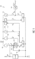
- FIG. 1 illustrates, in simplified schematic diagram form, an example current sense circuit 100 in accordance with an embodiment.
- Current sense circuit 100 is formed as an integrated circuit and includes a current limiter circuit block 108, a current rectifier circuit 122 and 124, a clamp circuit block 120, an amplifier circuit block 118, current sources 102-106 and 116, and current mirrors 110-114.
- An input terminal labeled IN is coupled to sense an input current IIN and an output terminal labeled OUT is coupled for generating and providing an amplified current IOUT1 based on the sensed current IIN.
- Current source 204 is configured and arranged to generate a current I22.
- a first terminal of current source 204 is connected at node BB and a second terminal of current source 204 is connected at the VDD supply terminal.
- a current mirror 210 labeled CM11 is connected at the VSS supply terminal.
- a first current leg of current mirror 210 is connected at node BB and a second current leg of current mirror 210 is connected at node labeled CC.
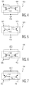
- Example implementations of current mirrors 210 and 212 are depicted in FIGs. 4-7 .
- the clamp circuit 220 includes a first terminal connected at the IN terminal and a second terminal connected at the VSS supply terminal.
- the clamp circuit 220 serves to protect circuitry coupled at the IN terminal.
- the input current IIN may be several orders of magnitude higher than during nominal operating conditions increasing or decreasing the input voltage to damaging levels.
- the clamp circuit 220 protects the circuitry coupled at the IN terminal by limiting the input voltage to predetermined voltage levels thus preventing damage.
- clamp circuit 220 may be implemented with a Zener diode having an anode terminal connected to the VSS supply terminal and a cathode terminal connected to the IN terminal.
- clamp circuit 220 may be implemented with other circuitry configured to clamp the voltage at the IN terminal.
- the current sense circuit may further include a second current source having a first terminal and a second terminal and configured to generate a second current, the first terminal coupled to the second leg of the first current mirror at a third node.
- the current sense circuit may further include a capacitor having a first terminal and a second terminal, the first terminal coupled at the first node and the second terminal coupled at the first voltage supply terminal.
- the current sense circuit may further include a clamp circuit having a first terminal and a second terminal, the first terminal coupled at the input terminal and the second terminal coupled at the first voltage supply terminal.
Landscapes
- Physics & Mathematics (AREA)
- General Physics & Mathematics (AREA)
- Engineering & Computer Science (AREA)
- Electromagnetism (AREA)
- Microelectronics & Electronic Packaging (AREA)
- Nonlinear Science (AREA)
- Radar, Positioning & Navigation (AREA)
- Automation & Control Theory (AREA)
- Control Of Electrical Variables (AREA)
Abstract
Description
- This disclosure relates generally to electronic circuits, and more specifically, to a current sense circuit.
- Today, many electronic products can be impacted by disturbances such as electro-magnetic interference. These electro-magnetic interference disturbances may cause sensitive circuitry, such as current sensing circuits, to operate abnormally. In turn, other circuitry relying on the outputs from these current sensing circuits may fail due to the abnormal operation. In safety critical situations, such abnormal operations may cause more dire consequences. Therefore, a need exists for current sensing circuits having a more robust tolerance to electro-magnetic interference disturbances.
- The present invention is illustrated by way of example and is not limited by the accompanying figures, in which like references indicate similar elements. Elements in the figures are illustrated for simplicity and clarity and have not necessarily been drawn to scale.
-
FIG. 1 illustrates, in simplified schematic diagram form, an example current sense circuit in accordance with an embodiment. -
FIG. 2 illustrates, in simplified schematic diagram form, an alternative example current sense circuit in accordance with an embodiment. -
FIG. 3 illustrates, in simplified schematic diagram form, an example implementation of a current limiter circuit in accordance with an embodiment. -
FIGs. 4-7 illustrate, in simplified schematic diagram form, example current mirror implementations in accordance with an embodiment. - Generally, there is provided, a current sense circuit configured and arranged to bound a sensed current with predetermined minimum and maximum currents, and thus improving robustness. By bounding the sensed current, subsequent stages are prevented from becoming unbiased due to lack of current. Having a bounded sensed current allows for a known output current during disturbance conditions such as electro-magnetic interference (EMI). Because the current sensing is based on current mirrors ratios, the current sense circuit is process, voltage, and temperature independent.
-
FIG. 1 illustrates, in simplified schematic diagram form, an examplecurrent sense circuit 100 in accordance with an embodiment.Current sense circuit 100 is formed as an integrated circuit and includes a currentlimiter circuit block 108, acurrent rectifier circuit clamp circuit block 120, anamplifier circuit block 118, current sources 102-106 and 116, and current mirrors 110-114. An input terminal labeled IN is coupled to sense an input current IIN and an output terminal labeled OUT is coupled for generating and providing an amplified current IOUT1 based on the sensed current IIN. -
Current source 102 is configured and arranged to generate a current I1. The current I1 is generated as a bias current IB multiplied by a ratio multiplier M (e.g., I1 = M x IB).Current source 102 includes a first terminal connected at the IN terminal and a second terminal connected to a voltage supply terminal labeled VDD. The rectifier circuit is connected at the IN terminal and includes adiode 122 and acapacitor 124. An anode terminal ofdiode 122 is connected at the IN terminal and a cathode terminal ofdiode 122 is connected to a first terminal ofcapacitor 124 at node labeled A. A second terminal ofcapacitor 124 is connected at a voltage supply terminal labeled VSS. An input terminal ofcurrent limiter 108 is connected at node A and an output terminal ofcurrent limiter 108 is connected at node labeled B. An example implementation ofcurrent limiter 108 is depicted inFIG. 3 . -
Current source 104 is configured and arranged to generate a current I2. The current I2 is generated as the bias current IB multiplied by a ratio multiplier L (e.g., I2 = L x IB). A first terminal ofcurrent source 104 is connected at node B and a second terminal ofcurrent source 104 is connected at the VDD supply terminal. Acurrent mirror 110 labeled CM1 is connected at the VSS supply terminal. A first current leg ofcurrent mirror 110 is connected at node B and a second current leg ofcurrent mirror 110 is connected at node labeled C. Example implementations of current mirrors 110-114 are depicted inFIGs. 4-7 . -
Current source 106 is configured and arranged to generate a current I3. The current I3 is generated as the bias current IB multiplied by a ratio multiplier N (e.g., I3 = N x IB).Current source 106 includes a first terminal connected at node C and a second terminal connected at the VDD supply terminal. A secondcurrent mirror 112 labeled CM2 is connected at the VDD supply terminal. A first current leg ofcurrent mirror 112 is connected at node C. A thirdcurrent mirror 114 labeled CM3 is connected at the VSS supply terminal. A second current leg ofcurrent mirror 112 is connected to a first current leg ofcurrent mirror 114 at node labeled D. A second current leg ofcurrent mirror 114 is connected at node labeled E.Current source 116 is configured and arranged to generate a current I9. The current I9 is generated as the bias current IB multiplied by a ratio multiplier P, where multiplier P is a sum of multipliers M + L - N + 1 (e.g., I9 = (M + L - N + 1) x IB). A first terminal of a fourthcurrent source 116 is connected at node E and a second terminal ofcurrent source 116 is connected at the VDD supply terminal. An output error current IE1 at a current branch labeled IE1 connected at node E is provided by current I9 minus current I8. - The
amplifier circuit block 118 includes an input terminal connected at node E to receive an input current labeled IE1 and an output terminal connected at the OUT terminal to provide an output current labeled IOUT1. Theamplifier circuit 118 serves as a gain stage and is configured to generate the IOUT1 current as an amplified or multiplied received input current IE1. In this embodiment, theamplifier circuit 118 may be implemented with any suitable circuitry (e.g., current mirror) for amplifying or multiplying the IE1 current received at the input terminal. In other embodiments, theamplifier circuit 118 may be implemented as a current to voltage converter providing an output voltage at the OUT terminal based on the IE1 current received. - The
clamp circuit 120 includes a first terminal connected at the IN terminal and a second terminal connected at the VSS supply terminal. Theclamp circuit 120 serves to protect circuitry coupled at the IN terminal. For example, during an EMI event, the input current IIN may be several orders of magnitude higher than during nominal operating conditions increasing or decreasing the input voltage to damaging levels. Theclamp circuit 120 protects the circuitry coupled at the IN terminal by limiting the input voltage to predetermined voltage levels thus preventing damage. In an embodiment,clamp circuit 120 may be implemented with a Zener diode having an anode terminal connected to the VSS supply terminal and a cathode terminal connected to the IN terminal. In other embodiments,clamp circuit 120 may be implemented with other circuitry configured to clamp the voltage at the IN terminal. - In the embodiment depicted in
FIG. 1 ,current sense circuit 100 is configured and arranged to generate an output error current IE1, for example, which is bound so that a minimum and maximum sensed current is known and predetermined by design. Having a bounded current allows for a known output current even during EMI disturbance conditions such as RF interference, and thus, prevents subsequent stages from becoming unbiased due to lack of current or excessive current. Further, the output current IE1, for example, can be kept constant under EMI conditions. -
Current source 102 is configured and arranged to generate current I1 which serves to allow detection of a negative IIN current. A minimum or lower bound sensed current (e.g., during disturbance conditions) occurs when current IIN is a negative current larger in magnitude than current I1 (e.g., IIN <= -I1).Diode 122 prevents negative current from propagating intocurrent limiter 108. A positive current ID throughdiode 122, provided by input current IIN plus current I1 (e.g., ID = IIN + I1), flows throughcurrent limiter 108 until a predetermined current limit value (ICLV) is reached.Current limiter 108 is configured and arranged to limit current to not exceed the ICLV and serves to provide a maximum or upper bound sensed current. A current I4 in the first current leg ofcurrent mirror 110 coupled at node B is provided by current ID plus current I2 (e.g., I4 = ID + I2) when ID is equal to or less than the ICLV. When the current ID is essentially zero (e.g., negative IIN current), the minimum or lower bound sensed current is current I4 provided by current I2 (e.g., I4 = I2). In turn, a mirrored current I5 is generated in the second current leg of current mirror 110 (e.g., I5 = ID + I2, ID <= ICLV). A current I6 in the first current leg ofcurrent mirror 112 coupled at node C is provided by current I5 minus current I3 (e.g., I6 = I5 - I3). In turn, a mirrored current I7 is generated in the second current leg of current mirror 112 (e.g., I7 = I5 - I3).Current mirror 114 is connected tocurrent mirror 112 at node D such that the current I7 flows in the first current leg ofcurrent mirror 114. In turn, a mirrored current I8 is generated in the second current leg of current mirror 114 (e.g., I8 = I5 - I3). Output current IE1 is provided by current I9 minus current I8 (e.g., IE1 = I9 - I8). Parameters such as ratio multipliers M, N, L, bias current IB, and ICLV serve to define a transfer function from input current IIN to the output error current IE1. -
FIG. 2 illustrates, in simplified schematic diagram form, an examplecurrent sense circuit 200 in accordance with an embodiment.Current sense circuit 200 is formed as an integrated circuit and includes a currentlimiter circuit block 208, acurrent rectifier circuit clamp circuit block 220, anamplifier circuit block 218, current sources 202-206 and 214, andcurrent mirrors -
Current source 202 is configured and arranged to generate a current I11. The current I11 is generated as a bias current IB multiplied by a ratio multiplier M (e.g., I11 = M x IB).Current source 202 includes a first terminal connected at the IN terminal and a second terminal connected to a voltage supply terminal labeled VDD. The rectifier circuit is connected at the IN terminal and includes adiode 222 and acapacitor 224. An anode terminal ofdiode 222 is connected at the IN terminal and a cathode terminal ofdiode 222 is connected to a first terminal ofcapacitor 224 at node labeled AA. A second terminal ofcapacitor 224 is connected at a voltage supply terminal labeled VSS. An input terminal ofcurrent limiter 208 is connected at node AA and an output terminal ofcurrent limiter 208 is connected at node labeled BB. An example implementation ofcurrent limiter 208 is depicted inFIG. 3 . -
Current source 204 is configured and arranged to generate a current I22. The current I22 is generated as the bias current IB multiplied by a ratio multiplier L (e.g., I22 = L x IB). A first terminal ofcurrent source 204 is connected at node BB and a second terminal ofcurrent source 204 is connected at the VDD supply terminal. Acurrent mirror 210 labeled CM11 is connected at the VSS supply terminal. A first current leg ofcurrent mirror 210 is connected at node BB and a second current leg ofcurrent mirror 210 is connected at node labeled CC. Example implementations ofcurrent mirrors FIGs. 4-7 . -
Current source 206 is configured and arranged to generate a current I33. The current I33 is generated as the bias current IB multiplied by a ratio multiplier N (e.g., I33 = N x IB).Current source 206 includes a first terminal connected at node CC and a second terminal connected at the VDD supply terminal. A secondcurrent mirror 212 labeled CM22 is connected at the VDD supply terminal. A first current leg ofcurrent mirror 212 is connected at node CC. A second current leg ofcurrent mirror 212 is connected at node labeled DD.Current source 214 is configured and arranged to source a current I88. The current I88 is generated as the bias current IB multiplied by a ratio multiplier Q, where multiplier Q is a first sum of multipliers M + L - N - 1 (e.g., I88 = (M + L - N - 1) x IB) or a second sum of multipliers M + L - N + 1 (e.g., I88 = (M + L - N + 1) x IB). A first terminal of a fourthcurrent source 214 is connected at node DD and a second terminal ofcurrent source 214 is connected at the VSS supply terminal. An output error current IE2 at a current branch labeled IE2 connected at node DD is provided by current I77 minus current I88. - The
amplifier circuit block 218 includes an input terminal connected at node DD to receive an input current labeled IE2 and an output terminal connected at the OUT terminal to provide an output current labeled IOUT2. Theamplifier circuit 218 serves as a gain stage and is configured to generate the IOUT2 current as an amplified or multiplied received input current IE2. In this embodiment, theamplifier circuit 218 may be implemented with any suitable circuitry (e.g., current mirror) for amplifying or multiplying the IE2 current received at the input terminal. In other embodiments, theamplifier circuit 218 may be implemented as a current to voltage converter providing an output voltage at the OUT terminal based on the IE2 current received. - The
clamp circuit 220 includes a first terminal connected at the IN terminal and a second terminal connected at the VSS supply terminal. Theclamp circuit 220 serves to protect circuitry coupled at the IN terminal. For example, during an EMI event, the input current IIN may be several orders of magnitude higher than during nominal operating conditions increasing or decreasing the input voltage to damaging levels. Theclamp circuit 220 protects the circuitry coupled at the IN terminal by limiting the input voltage to predetermined voltage levels thus preventing damage. In an embodiment,clamp circuit 220 may be implemented with a Zener diode having an anode terminal connected to the VSS supply terminal and a cathode terminal connected to the IN terminal. In other embodiments,clamp circuit 220 may be implemented with other circuitry configured to clamp the voltage at the IN terminal. - In the embodiment depicted in
FIG. 2 ,current sense circuit 200 is configured and arranged to generate an output current IE2, for example, which is bound so that a minimum and maximum sensed current is known and predetermined by design. Having a bounded current allows for a known output current even during EMI disturbance conditions such as RF interference, and thus, prevents subsequent stages from becoming unbiased due to lack of current or excessive current. Further, the output current IE2, for example, can be kept constant under EMI conditions. -
Current source 202 is configured and arranged to generate current I11 which serves to allow detection of a negative IIN current. A minimum or lower bound sensed current (e.g., during disturbance conditions) occurs when current IIN is a negative current larger in magnitude than current I11 (e.g., IIN <= -I11).Diode 222 prevents negative current from propagating intocurrent limiter 208. A current ID throughdiode 222, provided by input current IIN plus current I11 (e.g., ID = IIN + I11), flows throughcurrent limiter 208 until a predetermined current limit value (ICLV) is reached.Current limiter 208 is configured and arranged to limit current to not exceed the ICLV and serves to provide a maximum or upper bound sensed current. A current I44 in the first current leg ofcurrent mirror 210 coupled at node BB is provided by current ID plus current I22 (e.g., I44 = ID + I22) when ID is equal to or less than the ICLV. When the current ID is essentially zero (e.g., negative IIN current), the minimum or lower bound sensed current is current I4 provided by current I2 (e.g., I4 = I2). In turn, a mirrored current I55 is generated in the second current leg of current mirror 210 (e.g., I55 = ID + I22, ID <= ICLV). A current I66 in the first current leg ofcurrent mirror 212 coupled at node CC is provided by current I55 minus current I33 (e.g., I66 = I55 - I33). In turn, a mirrored current I77 is generated in the second current leg of current mirror 212 (e.g., I77 = I55 - I33). Output current IE2 is provided by current I77 minus current I88 (e.g., IE2 = I77-I88). Parameters such as ratio multipliers M, N, L, bias current IB, and ICLV serve to define a transfer function from input current IIN to the output error current IE2. -
FIG. 3 illustrates, in simplified schematic diagram form, an example implementation of acurrent limiter circuit 300 in accordance with an embodiment.Current limiter 300 is an example implementation of the current limiter circuit blocks 108 and 208 depicted inFIGs. 1 and2 , respectively. In this embodiment,current limiter 300 includescurrent sources current limiter 300 may be implemented by way of alternative circuitry.Current limiter 300 includes a first terminal labeled A/AA corresponding to the A and AA terminals ofFIGs. 1 and2 and a second terminal labeled B/BB corresponding to the B and BB terminals ofFIGs. 1 and2 . -
Current source 302 is configured and arranged to generate a current I302 (e.g., I302 = ICLV).Current source 302 includes a first terminal connected atnode 312 and a second terminal connected to the VDD supply terminal.Current source 304 is configured and arranged to generate a current I304 (e.g., I304 = L x IB).Current source 304 includes a first terminal connected atnode 314 and a second terminal connected to the VDD supply terminal. - A first current electrode of
transistor 306 is connected to control electrodes oftransistors node 312. A first current electrode oftransistor 310 is connected at the A/AA terminal and a second current electrode oftransistor 310 is connected at the B/BB terminal. A second current electrode oftransistor 306 is connected to a first current electrode and a control electrode oftransistor 308 atnode 314. A second current electrode oftransistor 308 is connected to the VSS supply terminal. In this arrangement,transistor 308 is configured as a diode. - In the embodiment depicted in
FIG. 3 ,current sources transistors node 312.Transistor 310 serves to control the amount of current flowing between terminals A/AA and B/BB based on the bias voltage applied to the control electrode oftransistor 310 connected atnode 312. The bias voltage generated atnode 312 is a predetermined value chosen such that a desired current limit value is realized. -
FIGs. 4-7 illustrate, in simplified schematic diagram form, example current mirror implementations for current mirrors 110-114 and 210 and 212 depicted inFIGs. 1 and2 , respectively, in accordance with an embodiment. More specifically, the circuits illustrated inFIGs. 4 and 5 are example implementations forcurrent mirrors FIGs. 1 and2 and the circuits illustrated inFIGs. 6 and 7 are example implementations forcurrent mirrors FIGs. 1 and2 . In other embodiments, current mirrors 110-114 and 210 and 212 may be implemented by way of alternative circuitry. -
FIG. 4 depicts examplecurrent mirror 400 implemented with N-channel transistors transistor 402 having a current path betweennode 406 and the VSS supply terminal, and a second current leg includestransistor 404 having a current path betweennode 408 and the VSS supply terminal.Current mirror 400 is configured and arranged to generate a mirrored current in the second current leg based on a current in the first current leg. A first current electrode oftransistor 402 is connected to control electrodes oftransistors node 406. A first current electrode oftransistor 404 is connected atnode 408 and second current electrodes oftransistors -
FIG. 5 depicts examplecurrent mirror 500 implemented with NPNbipolar transistors transistor 502 having a current path betweennode 506 and the VSS supply terminal, and a second current leg includestransistor 504 having a current path betweennode 508 and the VSS supply terminal.Current mirror 500 is configured and arranged to generate a mirrored current in the second current leg based on a current in the first current leg. A first current electrode oftransistor 502 is connected to control electrodes oftransistors node 506. A first current electrode oftransistor 504 is connected atnode 508 and second current electrodes oftransistors -
FIG. 6 depicts examplecurrent mirror 600 implemented with P-channel transistors transistor 602 having a current path between node 606 and the VDD supply terminal, and a second current leg includestransistor 604 having a current path betweennode 608 and the VDD supply terminal.Current mirror 600 is configured and arranged to generate a mirrored current in the second current leg based on a current in the first current leg. A first current electrode oftransistor 602 is connected to control electrodes oftransistors transistor 604 is connected atnode 608 and second current electrodes oftransistors -
FIG. 7 depicts examplecurrent mirror 700 implemented with PNPbipolar transistors transistor 702 having a current path betweennode 706 and the VDD supply terminal, and a second current leg includestransistor 704 having a current path betweennode 708 and the VDD supply terminal.Current mirror 700 is configured and arranged to generate a mirrored current in the second current leg based on a current in the first current leg. A first current electrode oftransistor 702 is connected to control electrodes oftransistors node 706. A first current electrode oftransistor 704 is connected atnode 708 and second current electrodes oftransistors - Generally, there is provided, a current sense circuit including an input terminal coupled to sense an input current; a diode having a first terminal and a second terminal, the first terminal coupled at the input terminal; a current limiter having a first terminal and a second terminal, the first terminal coupled to the second terminal of the diode at a first node; a first current source having a first terminal and a second terminal and configured to generate a first current, the first terminal coupled to the second terminal of the current limiter at a second node; and a first current mirror coupled to a first voltage supply terminal and having a first leg and a second leg, the first leg coupled at the second node and the second leg coupled for generating a first output current. The current sense circuit may further include a second current source having a first terminal and a second terminal and configured to generate a second current, the first terminal coupled to the second leg of the first current mirror at a third node. The current sense circuit may further include a capacitor having a first terminal and a second terminal, the first terminal coupled at the first node and the second terminal coupled at the first voltage supply terminal. The current sense circuit may further include a clamp circuit having a first terminal and a second terminal, the first terminal coupled at the input terminal and the second terminal coupled at the first voltage supply terminal. The current limiter may include a first transistor having a first current electrode coupled at the first node and a second current electrode coupled at the second node; a second transistor having a first current electrode coupled to control electrodes of the first transistor and the second transistor; and a third transistor configured as a second diode having a first current electrode and a control electrode coupled to a second current electrode of the second transistor. The current sense circuit may further include a second current mirror coupled to a second voltage supply terminal and having a first leg and a second leg, the first leg coupled to the second leg of the first current mirror and the second leg coupled for generating a mirrored current of the first output current. The current sense circuit may further include an amplifier circuit having an input coupled to the second leg of the second current mirror and an output coupled for generating an amplified current based on the first output current. The current sense circuit may further include a third current mirror coupled to the first voltage supply terminal and having a first leg and a second leg, the first leg coupled to the second leg of the second current mirror and the second leg coupled for generating a second output current based on a mirrored current of the first leg. The current sense circuit may further include a third current source having a first terminal and a second terminal, the first terminal coupled at the input terminal and configured to generate a third current.
- In another embodiment, there is provided, a current sense circuit including a diode having an anode terminal coupled to an input terminal and a cathode terminal, the input terminal coupled for sensing an input current; a current limiter having a first terminal and a second terminal, the first terminal coupled to the cathode terminal of the diode at a first node; a first current mirror coupled to a first voltage supply terminal and having a first leg and a second leg, the first leg coupled to the second terminal of the current limiter at a second node; a first current source including a first terminal and a second terminal and configured to generate a first current, the first terminal coupled at the second node; a second current source including a first terminal and a second terminal and configured to generate a second current, the first terminal coupled to the second leg of the first current mirror at a third node; and a first current branch coupled at the third node, the first current branch coupled for generating a first output current. The current sense circuit may further include a second current mirror coupled to a second voltage supply terminal and having a first leg and a second leg, the first leg coupled to the third node by way of the first current branch and the second leg coupled for generating a second output current, the second output current a mirrored current of the first output current. The current limiter may include a first transistor having a first current electrode coupled at the first node and a second current electrode coupled at the second node; a second transistor having a first current electrode coupled to control electrodes of the first transistor and the second transistor; and a third current source including a first terminal coupled to the first current electrode of the second transistor, the third current source configured to generate a third current. The current sense circuit may further include a capacitor having a first terminal and a second terminal, the first terminal coupled at the first node and the second terminal coupled at the first voltage supply terminal. The current sense circuit may further include a clamp circuit having a first terminal and a second terminal, the first terminal coupled at the input terminal and the second terminal coupled at the first voltage supply terminal. The clamp circuit may include a Zener diode coupled to the first voltage supply terminal. The current sense circuit may further include a third current source including a first terminal coupled at the input terminal, the third current source configured to generate a third current. The first output current may be bound at a lower limit based on the third current.
- In yet another embodiment, there is provided, a current sense circuit including a current rectifier circuit having a first terminal coupled to an input terminal, the input terminal coupled for sensing an input current; a current limiter having a first terminal and a second terminal, the first terminal coupled to a second terminal of the current rectifier circuit at a first node; a first current mirror coupled to a first voltage supply terminal and having a first leg and a second leg, the first leg coupled to the second terminal of the current limiter at a second node; a first current source having a first terminal and a second terminal and configured to generate a first current, the first terminal coupled at the second node; a second current source having a first terminal and a second terminal and configured to generate a second current, the first terminal coupled to the second leg of the first current mirror at a third node; and a first current branch coupled at the third node, the first current branch coupled for generating a first output current. The current sense circuit may further include a diode having an anode terminal coupled to the input terminal and a cathode terminal coupled at the first node; and a capacitor having a first terminal coupled at the first node and a second terminal coupled at the first voltage supply terminal. The first current mirror and the second current source may be configured and arranged such that the first output current is a current in the second leg of the first current mirror minus the second current.
- By now it should be appreciated that there has been provided, a current sense circuit configured and arranged to bound a sensed current with predetermined minimum and maximum currents, and thus improving robustness. By bounding the sensed current, subsequent stages are prevented from becoming unbiased due to lack of current or excessive current. Having a bounded sensed current allows for a known output current during disturbance conditions such as electro-magnetic interference (EMI). Because the current sensing is based on current mirrors ratios, the current sense circuit is process, voltage, and temperature independent.
- Because the apparatus implementing the present invention is, for the most part, composed of electronic components and circuits known to those skilled in the art, circuit details will not be explained in any greater extent than that considered necessary as illustrated above, for the understanding and appreciation of the underlying concepts of the present invention and in order not to obfuscate or distract from the teachings of the present invention.
- Although the invention is described herein with reference to specific embodiments, various modifications and changes can be made without departing from the scope of the present invention as set forth in the claims below. Accordingly, the specification and figures are to be regarded in an illustrative rather than a restrictive sense, and all such modifications are intended to be included within the scope of the present invention. Any benefits, advantages, or solutions to problems that are described herein with regard to specific embodiments are not intended to be construed as a critical, required, or essential feature or element of any or all the claims.
- Furthermore, the terms "a" or "an," as used herein, are defined as one or more than one. Also, the use of introductory phrases such as "at least one" and "one or more" in the claims should not be construed to imply that the introduction of another claim element by the indefinite articles "a" or "an" limits any particular claim containing such introduced claim element to inventions containing only one such element, even when the same claim includes the introductory phrases "one or more" or "at least one" and indefinite articles such as "a" or "an." The same holds true for the use of definite articles.
- Unless stated otherwise, terms such as "first" and "second" are used to arbitrarily distinguish between the elements such terms describe. Thus, these terms are not necessarily intended to indicate temporal or other prioritization of such elements.
Claims (9)
- A current sense circuit comprising:an input terminal coupled to sense an input current;a diode having a first terminal and a second terminal, the first terminal coupled at the input terminal;a current limiter having a first terminal and a second terminal, the first terminal coupled to the second terminal of the diode at a first node;a first current source having a first terminal and a second terminal and configured to generate a first current, the first terminal coupled to the second terminal of the current limiter at a second node; anda first current mirror coupled to a first voltage supply terminal and having a first leg and a second leg, the first leg coupled at the second node and the second leg coupled for generating a first output current.
- The current sense circuit of claim 1, further comprising:
a second current source having a first terminal and a second terminal and configured to generate a second current, the first terminal coupled to the second leg of the first current mirror at a third node. - The current sense circuit of claim 1 or 2, further comprising:
a capacitor having a first terminal and a second terminal, the first terminal coupled at the first node and the second terminal coupled at the first voltage supply terminal. - The current sense circuit of any preceding claim, further comprising:
a clamp circuit having a first terminal and a second terminal, the first terminal coupled at the input terminal and the second terminal coupled at the first voltage supply terminal. - The current sense circuit of any preceding claim, wherein the current limiter comprises:a first transistor having a first current electrode coupled at the first node and a second current electrode coupled at the second node;a second transistor having a first current electrode coupled to control electrodes of the first transistor and the second transistor; and a third transistor configured as a second diode having a first current electrode and a control electrode coupled to a second current electrode of the second transistor.
- The current sense circuit of any preceding claim, further comprising:
a second current mirror coupled to a second voltage supply terminal and having a first leg and a second leg, the first leg coupled to the second leg of the first current mirror and the second leg coupled for generating a mirrored current of the first output current. - The current sense circuit of claim 6, further comprising:
an amplifier circuit having an input coupled to the second leg of the second current mirror and an output coupled for generating an amplified current based on the first output current. - The current sense circuit of claim 6 or 7, further comprising:
a third current mirror coupled to the first voltage supply terminal and having a first leg and a second leg, the first leg coupled to the second leg of the second current mirror and the second leg coupled for generating a second output current based on a mirrored current of the first leg. - The current sense circuit of any preceding claim, further comprising:
a third current source having a first terminal and a second terminal, the first terminal coupled at the input terminal and configured to generate a third current.
Applications Claiming Priority (1)
| Application Number | Priority Date | Filing Date | Title |
|---|---|---|---|
| US16/522,785 US11079414B2 (en) | 2019-07-26 | 2019-07-26 | Current sense circuit and method thereof |
Publications (2)
| Publication Number | Publication Date |
|---|---|
| EP3770613A1 true EP3770613A1 (en) | 2021-01-27 |
| EP3770613B1 EP3770613B1 (en) | 2022-04-13 |
Family
ID=71614686
Family Applications (1)
| Application Number | Title | Priority Date | Filing Date |
|---|---|---|---|
| EP20185427.0A Active EP3770613B1 (en) | 2019-07-26 | 2020-07-13 | Current sense circuit and method thereof |
Country Status (3)
| Country | Link |
|---|---|
| US (1) | US11079414B2 (en) |
| EP (1) | EP3770613B1 (en) |
| CN (1) | CN112305292A (en) |
Families Citing this family (2)
| Publication number | Priority date | Publication date | Assignee | Title |
|---|---|---|---|---|
| CN113484595B (en) * | 2021-07-09 | 2022-06-10 | 江南大学 | Current reading system and method for memory operation memory unit |
| US12375076B2 (en) | 2023-04-05 | 2025-07-29 | Nxp B.V. | Leakage current compensation |
Citations (4)
| Publication number | Priority date | Publication date | Assignee | Title |
|---|---|---|---|---|
| US20160147247A1 (en) * | 2014-11-20 | 2016-05-26 | Qualcomm Incorporated | Low voltage, highly accurate current mirror |
| US20160233666A1 (en) * | 2015-02-06 | 2016-08-11 | Sandia Corporation | Current limiter circuit system |
| US20160320433A1 (en) * | 2015-04-29 | 2016-11-03 | Delta Electronics, Inc. | High side current monitoring apparatus |
| US10228713B1 (en) * | 2017-12-21 | 2019-03-12 | Texas Instruments Incorporated | Large range current mirror |
Family Cites Families (8)
| Publication number | Priority date | Publication date | Assignee | Title |
|---|---|---|---|---|
| US5262713A (en) * | 1991-01-31 | 1993-11-16 | Texas Instruments Incorporated | Current mirror for sensing current |
| US5414583A (en) * | 1991-12-19 | 1995-05-09 | Unitrode Corporation | Current source bus terminator with voltage clamping and steady state power reduction |
| DE10146849A1 (en) * | 2001-09-24 | 2003-04-10 | Atmel Germany Gmbh | Process for generating an output voltage |
| US7535691B2 (en) * | 2006-03-30 | 2009-05-19 | Power Integrations, Inc. | Method and apparatus for an in-rush current limiting circuit |
| US7960997B2 (en) * | 2007-08-08 | 2011-06-14 | Advanced Analogic Technologies, Inc. | Cascode current sensor for discrete power semiconductor devices |
| US7893670B2 (en) * | 2009-02-20 | 2011-02-22 | Standard Microsystems Corporation | Frequency compensation scheme for stabilizing the LDO using external NPN in HV domain |
| TWI496504B (en) * | 2013-04-26 | 2015-08-11 | Unity Opto Technology Co Ltd | Variable power dimming control circuit |
| US11095111B2 (en) * | 2018-04-02 | 2021-08-17 | Allegro Microsystems, Llc | Systems and methods for transient pulse protection |
-
2019
- 2019-07-26 US US16/522,785 patent/US11079414B2/en not_active Expired - Fee Related
-
2020
- 2020-07-13 EP EP20185427.0A patent/EP3770613B1/en active Active
- 2020-07-20 CN CN202010701753.0A patent/CN112305292A/en not_active Withdrawn
Patent Citations (4)
| Publication number | Priority date | Publication date | Assignee | Title |
|---|---|---|---|---|
| US20160147247A1 (en) * | 2014-11-20 | 2016-05-26 | Qualcomm Incorporated | Low voltage, highly accurate current mirror |
| US20160233666A1 (en) * | 2015-02-06 | 2016-08-11 | Sandia Corporation | Current limiter circuit system |
| US20160320433A1 (en) * | 2015-04-29 | 2016-11-03 | Delta Electronics, Inc. | High side current monitoring apparatus |
| US10228713B1 (en) * | 2017-12-21 | 2019-03-12 | Texas Instruments Incorporated | Large range current mirror |
Also Published As
| Publication number | Publication date |
|---|---|
| US20210025923A1 (en) | 2021-01-28 |
| CN112305292A (en) | 2021-02-02 |
| US11079414B2 (en) | 2021-08-03 |
| EP3770613B1 (en) | 2022-04-13 |
Similar Documents
| Publication | Publication Date | Title |
|---|---|---|
| US5589759A (en) | Circuit for detecting voltage variations in relation to a set value, for devices comprising error amplifiers | |
| US5831471A (en) | DC-stabilized power circuit | |
| US7135842B2 (en) | Voltage regulator having improved IR drop | |
| KR102252365B1 (en) | Overheat protection circuit and voltage regulator | |
| US10061334B2 (en) | Voltage regulator | |
| KR100888483B1 (en) | Reference bias circuit compensates for process variation | |
| EP3770613B1 (en) | Current sense circuit and method thereof | |
| KR20080025284A (en) | Temperature detector | |
| US20100289464A1 (en) | Power supply circuit | |
| US10901009B2 (en) | Power detector for radiofrequency power amplifier circuits | |
| US6600639B1 (en) | Precision low voltage supply system and method with undervoltage lockout capabilities | |
| CN114157252A (en) | Power amplifying circuit and radio frequency signal processing method | |
| US5059921A (en) | Amplifier having two operating modes | |
| US5568547A (en) | Subscriber circuit provided with a circuit for monitoring a subscriber instrument | |
| US11996830B2 (en) | Power switch reverse current protection systems | |
| EP4135196A1 (en) | Digital output circuit, digital output device, and digital output system | |
| US3122694A (en) | Current limiter utilizing a small ohmic resistance in series with the load | |
| US9454174B2 (en) | Power supply voltage monitoring circuit, and electronic circuit including the power supply voltage monitoring circuit | |
| KR20180129477A (en) | Envelope-tracking current bias circuit with offset cancellation function | |
| US10627838B1 (en) | Comparator with adaptive sense voltage clamp | |
| US11139786B2 (en) | Amplifying device with adaptive CTAT biasing control | |
| KR101091718B1 (en) | Detection circuit, detection method and computer readable medium | |
| US20050093596A1 (en) | Power supply apparatus for delay locked loop and method thereof | |
| US10488446B2 (en) | Power detector | |
| CN111142603A (en) | Circuit and device for detecting reference voltage bjt tube temperature saving |
Legal Events
| Date | Code | Title | Description |
|---|---|---|---|
| PUAI | Public reference made under article 153(3) epc to a published international application that has entered the european phase |
Free format text: ORIGINAL CODE: 0009012 |
|
| STAA | Information on the status of an ep patent application or granted ep patent |
Free format text: STATUS: THE APPLICATION HAS BEEN PUBLISHED |
|
| AK | Designated contracting states |
Kind code of ref document: A1 Designated state(s): AL AT BE BG CH CY CZ DE DK EE ES FI FR GB GR HR HU IE IS IT LI LT LU LV MC MK MT NL NO PL PT RO RS SE SI SK SM TR |
|
| AX | Request for extension of the european patent |
Extension state: BA ME |
|
| STAA | Information on the status of an ep patent application or granted ep patent |
Free format text: STATUS: REQUEST FOR EXAMINATION WAS MADE |
|
| 17P | Request for examination filed |
Effective date: 20210727 |
|
| RBV | Designated contracting states (corrected) |
Designated state(s): AL AT BE BG CH CY CZ DE DK EE ES FI FR GB GR HR HU IE IS IT LI LT LU LV MC MK MT NL NO PL PT RO RS SE SI SK SM TR |
|
| GRAP | Despatch of communication of intention to grant a patent |
Free format text: ORIGINAL CODE: EPIDOSNIGR1 |
|
| STAA | Information on the status of an ep patent application or granted ep patent |
Free format text: STATUS: GRANT OF PATENT IS INTENDED |
|
| INTG | Intention to grant announced |
Effective date: 20220120 |
|
| GRAS | Grant fee paid |
Free format text: ORIGINAL CODE: EPIDOSNIGR3 |
|
| GRAA | (expected) grant |
Free format text: ORIGINAL CODE: 0009210 |
|
| STAA | Information on the status of an ep patent application or granted ep patent |
Free format text: STATUS: THE PATENT HAS BEEN GRANTED |
|
| AK | Designated contracting states |
Kind code of ref document: B1 Designated state(s): AL AT BE BG CH CY CZ DE DK EE ES FI FR GB GR HR HU IE IS IT LI LT LU LV MC MK MT NL NO PL PT RO RS SE SI SK SM TR |
|
| REG | Reference to a national code |
Ref country code: GB Ref legal event code: FG4D |
|
| REG | Reference to a national code |
Ref country code: CH Ref legal event code: EP |
|
| REG | Reference to a national code |
Ref country code: DE Ref legal event code: R096 Ref document number: 602020002640 Country of ref document: DE |
|
| REG | Reference to a national code |
Ref country code: IE Ref legal event code: FG4D |
|
| REG | Reference to a national code |
Ref country code: AT Ref legal event code: REF Ref document number: 1483798 Country of ref document: AT Kind code of ref document: T Effective date: 20220515 |
|
| REG | Reference to a national code |
Ref country code: LT Ref legal event code: MG9D |
|
| REG | Reference to a national code |
Ref country code: NL Ref legal event code: MP Effective date: 20220413 |
|
| REG | Reference to a national code |
Ref country code: AT Ref legal event code: MK05 Ref document number: 1483798 Country of ref document: AT Kind code of ref document: T Effective date: 20220413 |
|
| PG25 | Lapsed in a contracting state [announced via postgrant information from national office to epo] |
Ref country code: NL Free format text: LAPSE BECAUSE OF FAILURE TO SUBMIT A TRANSLATION OF THE DESCRIPTION OR TO PAY THE FEE WITHIN THE PRESCRIBED TIME-LIMIT Effective date: 20220413 |
|
| PG25 | Lapsed in a contracting state [announced via postgrant information from national office to epo] |
Ref country code: SE Free format text: LAPSE BECAUSE OF FAILURE TO SUBMIT A TRANSLATION OF THE DESCRIPTION OR TO PAY THE FEE WITHIN THE PRESCRIBED TIME-LIMIT Effective date: 20220413 Ref country code: PT Free format text: LAPSE BECAUSE OF FAILURE TO SUBMIT A TRANSLATION OF THE DESCRIPTION OR TO PAY THE FEE WITHIN THE PRESCRIBED TIME-LIMIT Effective date: 20220816 Ref country code: NO Free format text: LAPSE BECAUSE OF FAILURE TO SUBMIT A TRANSLATION OF THE DESCRIPTION OR TO PAY THE FEE WITHIN THE PRESCRIBED TIME-LIMIT Effective date: 20220713 Ref country code: LT Free format text: LAPSE BECAUSE OF FAILURE TO SUBMIT A TRANSLATION OF THE DESCRIPTION OR TO PAY THE FEE WITHIN THE PRESCRIBED TIME-LIMIT Effective date: 20220413 Ref country code: HR Free format text: LAPSE BECAUSE OF FAILURE TO SUBMIT A TRANSLATION OF THE DESCRIPTION OR TO PAY THE FEE WITHIN THE PRESCRIBED TIME-LIMIT Effective date: 20220413 Ref country code: GR Free format text: LAPSE BECAUSE OF FAILURE TO SUBMIT A TRANSLATION OF THE DESCRIPTION OR TO PAY THE FEE WITHIN THE PRESCRIBED TIME-LIMIT Effective date: 20220714 Ref country code: FI Free format text: LAPSE BECAUSE OF FAILURE TO SUBMIT A TRANSLATION OF THE DESCRIPTION OR TO PAY THE FEE WITHIN THE PRESCRIBED TIME-LIMIT Effective date: 20220413 Ref country code: ES Free format text: LAPSE BECAUSE OF FAILURE TO SUBMIT A TRANSLATION OF THE DESCRIPTION OR TO PAY THE FEE WITHIN THE PRESCRIBED TIME-LIMIT Effective date: 20220413 Ref country code: BG Free format text: LAPSE BECAUSE OF FAILURE TO SUBMIT A TRANSLATION OF THE DESCRIPTION OR TO PAY THE FEE WITHIN THE PRESCRIBED TIME-LIMIT Effective date: 20220713 Ref country code: AT Free format text: LAPSE BECAUSE OF FAILURE TO SUBMIT A TRANSLATION OF THE DESCRIPTION OR TO PAY THE FEE WITHIN THE PRESCRIBED TIME-LIMIT Effective date: 20220413 |
|
| PG25 | Lapsed in a contracting state [announced via postgrant information from national office to epo] |
Ref country code: RS Free format text: LAPSE BECAUSE OF FAILURE TO SUBMIT A TRANSLATION OF THE DESCRIPTION OR TO PAY THE FEE WITHIN THE PRESCRIBED TIME-LIMIT Effective date: 20220413 Ref country code: PL Free format text: LAPSE BECAUSE OF FAILURE TO SUBMIT A TRANSLATION OF THE DESCRIPTION OR TO PAY THE FEE WITHIN THE PRESCRIBED TIME-LIMIT Effective date: 20220413 Ref country code: LV Free format text: LAPSE BECAUSE OF FAILURE TO SUBMIT A TRANSLATION OF THE DESCRIPTION OR TO PAY THE FEE WITHIN THE PRESCRIBED TIME-LIMIT Effective date: 20220413 Ref country code: IS Free format text: LAPSE BECAUSE OF FAILURE TO SUBMIT A TRANSLATION OF THE DESCRIPTION OR TO PAY THE FEE WITHIN THE PRESCRIBED TIME-LIMIT Effective date: 20220813 |
|
| REG | Reference to a national code |
Ref country code: DE Ref legal event code: R097 Ref document number: 602020002640 Country of ref document: DE |
|
| PG25 | Lapsed in a contracting state [announced via postgrant information from national office to epo] |
Ref country code: SM Free format text: LAPSE BECAUSE OF FAILURE TO SUBMIT A TRANSLATION OF THE DESCRIPTION OR TO PAY THE FEE WITHIN THE PRESCRIBED TIME-LIMIT Effective date: 20220413 Ref country code: SK Free format text: LAPSE BECAUSE OF FAILURE TO SUBMIT A TRANSLATION OF THE DESCRIPTION OR TO PAY THE FEE WITHIN THE PRESCRIBED TIME-LIMIT Effective date: 20220413 Ref country code: RO Free format text: LAPSE BECAUSE OF FAILURE TO SUBMIT A TRANSLATION OF THE DESCRIPTION OR TO PAY THE FEE WITHIN THE PRESCRIBED TIME-LIMIT Effective date: 20220413 Ref country code: EE Free format text: LAPSE BECAUSE OF FAILURE TO SUBMIT A TRANSLATION OF THE DESCRIPTION OR TO PAY THE FEE WITHIN THE PRESCRIBED TIME-LIMIT Effective date: 20220413 Ref country code: DK Free format text: LAPSE BECAUSE OF FAILURE TO SUBMIT A TRANSLATION OF THE DESCRIPTION OR TO PAY THE FEE WITHIN THE PRESCRIBED TIME-LIMIT Effective date: 20220413 Ref country code: CZ Free format text: LAPSE BECAUSE OF FAILURE TO SUBMIT A TRANSLATION OF THE DESCRIPTION OR TO PAY THE FEE WITHIN THE PRESCRIBED TIME-LIMIT Effective date: 20220413 |
|
| PLBE | No opposition filed within time limit |
Free format text: ORIGINAL CODE: 0009261 |
|
| STAA | Information on the status of an ep patent application or granted ep patent |
Free format text: STATUS: NO OPPOSITION FILED WITHIN TIME LIMIT |
|
| PG25 | Lapsed in a contracting state [announced via postgrant information from national office to epo] |
Ref country code: MC Free format text: LAPSE BECAUSE OF FAILURE TO SUBMIT A TRANSLATION OF THE DESCRIPTION OR TO PAY THE FEE WITHIN THE PRESCRIBED TIME-LIMIT Effective date: 20220413 |
|
| 26N | No opposition filed |
Effective date: 20230116 |
|
| REG | Reference to a national code |
Ref country code: BE Ref legal event code: MM Effective date: 20220731 |
|
| PG25 | Lapsed in a contracting state [announced via postgrant information from national office to epo] |
Ref country code: AL Free format text: LAPSE BECAUSE OF FAILURE TO SUBMIT A TRANSLATION OF THE DESCRIPTION OR TO PAY THE FEE WITHIN THE PRESCRIBED TIME-LIMIT Effective date: 20220413 |
|
| PG25 | Lapsed in a contracting state [announced via postgrant information from national office to epo] |
Ref country code: LU Free format text: LAPSE BECAUSE OF NON-PAYMENT OF DUE FEES Effective date: 20220713 |
|
| PG25 | Lapsed in a contracting state [announced via postgrant information from national office to epo] |
Ref country code: SI Free format text: LAPSE BECAUSE OF FAILURE TO SUBMIT A TRANSLATION OF THE DESCRIPTION OR TO PAY THE FEE WITHIN THE PRESCRIBED TIME-LIMIT Effective date: 20220413 Ref country code: BE Free format text: LAPSE BECAUSE OF NON-PAYMENT OF DUE FEES Effective date: 20220731 |
|
| PG25 | Lapsed in a contracting state [announced via postgrant information from national office to epo] |
Ref country code: IE Free format text: LAPSE BECAUSE OF NON-PAYMENT OF DUE FEES Effective date: 20220713 |
|
| P01 | Opt-out of the competence of the unified patent court (upc) registered |
Effective date: 20230725 |
|
| PG25 | Lapsed in a contracting state [announced via postgrant information from national office to epo] |
Ref country code: IT Free format text: LAPSE BECAUSE OF FAILURE TO SUBMIT A TRANSLATION OF THE DESCRIPTION OR TO PAY THE FEE WITHIN THE PRESCRIBED TIME-LIMIT Effective date: 20220413 |
|
| REG | Reference to a national code |
Ref country code: CH Ref legal event code: PL |
|
| PG25 | Lapsed in a contracting state [announced via postgrant information from national office to epo] |
Ref country code: MK Free format text: LAPSE BECAUSE OF FAILURE TO SUBMIT A TRANSLATION OF THE DESCRIPTION OR TO PAY THE FEE WITHIN THE PRESCRIBED TIME-LIMIT Effective date: 20220413 Ref country code: CY Free format text: LAPSE BECAUSE OF FAILURE TO SUBMIT A TRANSLATION OF THE DESCRIPTION OR TO PAY THE FEE WITHIN THE PRESCRIBED TIME-LIMIT Effective date: 20220413 Ref country code: CH Free format text: LAPSE BECAUSE OF NON-PAYMENT OF DUE FEES Effective date: 20230731 |
|
| PG25 | Lapsed in a contracting state [announced via postgrant information from national office to epo] |
Ref country code: HU Free format text: LAPSE BECAUSE OF FAILURE TO SUBMIT A TRANSLATION OF THE DESCRIPTION OR TO PAY THE FEE WITHIN THE PRESCRIBED TIME-LIMIT; INVALID AB INITIO Effective date: 20200713 |
|
| PGFP | Annual fee paid to national office [announced via postgrant information from national office to epo] |
Ref country code: GB Payment date: 20240620 Year of fee payment: 5 |
|
| PGFP | Annual fee paid to national office [announced via postgrant information from national office to epo] |
Ref country code: FR Payment date: 20240619 Year of fee payment: 5 |
|
| PG25 | Lapsed in a contracting state [announced via postgrant information from national office to epo] |
Ref country code: MT Free format text: LAPSE BECAUSE OF FAILURE TO SUBMIT A TRANSLATION OF THE DESCRIPTION OR TO PAY THE FEE WITHIN THE PRESCRIBED TIME-LIMIT Effective date: 20220413 |
|
| PGFP | Annual fee paid to national office [announced via postgrant information from national office to epo] |
Ref country code: DE Payment date: 20240619 Year of fee payment: 5 |
|
| PG25 | Lapsed in a contracting state [announced via postgrant information from national office to epo] |
Ref country code: BG Free format text: LAPSE BECAUSE OF FAILURE TO SUBMIT A TRANSLATION OF THE DESCRIPTION OR TO PAY THE FEE WITHIN THE PRESCRIBED TIME-LIMIT Effective date: 20220413 |
|
| PG25 | Lapsed in a contracting state [announced via postgrant information from national office to epo] |
Ref country code: BG Free format text: LAPSE BECAUSE OF FAILURE TO SUBMIT A TRANSLATION OF THE DESCRIPTION OR TO PAY THE FEE WITHIN THE PRESCRIBED TIME-LIMIT Effective date: 20220413 |
|
| PG25 | Lapsed in a contracting state [announced via postgrant information from national office to epo] |
Ref country code: TR Free format text: LAPSE BECAUSE OF FAILURE TO SUBMIT A TRANSLATION OF THE DESCRIPTION OR TO PAY THE FEE WITHIN THE PRESCRIBED TIME-LIMIT Effective date: 20220413 |
|
| REG | Reference to a national code |
Ref country code: DE Ref legal event code: R119 Ref document number: 602020002640 Country of ref document: DE |
|
| GBPC | Gb: european patent ceased through non-payment of renewal fee |
Effective date: 20250713 |
|
| PG25 | Lapsed in a contracting state [announced via postgrant information from national office to epo] |
Ref country code: GB Free format text: LAPSE BECAUSE OF NON-PAYMENT OF DUE FEES Effective date: 20250713 |
|
| PG25 | Lapsed in a contracting state [announced via postgrant information from national office to epo] |
Ref country code: DE Free format text: LAPSE BECAUSE OF NON-PAYMENT OF DUE FEES Effective date: 20260203 |
|
| PG25 | Lapsed in a contracting state [announced via postgrant information from national office to epo] |
Ref country code: FR Free format text: LAPSE BECAUSE OF NON-PAYMENT OF DUE FEES Effective date: 20250731 |