EP3769903A1 - Process for preparing a processed filament by interaction of a filament with at least one processing beam in n processing steps - Google Patents
Process for preparing a processed filament by interaction of a filament with at least one processing beam in n processing steps Download PDFInfo
- Publication number
- EP3769903A1 EP3769903A1 EP20187767.7A EP20187767A EP3769903A1 EP 3769903 A1 EP3769903 A1 EP 3769903A1 EP 20187767 A EP20187767 A EP 20187767A EP 3769903 A1 EP3769903 A1 EP 3769903A1
- Authority
- EP
- European Patent Office
- Prior art keywords
- filament
- processing
- segment
- section
- processing beam
- Prior art date
- Legal status (The legal status is an assumption and is not a legal conclusion. Google has not performed a legal analysis and makes no representation as to the accuracy of the status listed.)
- Pending
Links
Images









Classifications
-
- B—PERFORMING OPERATIONS; TRANSPORTING
- B23—MACHINE TOOLS; METAL-WORKING NOT OTHERWISE PROVIDED FOR
- B23K—SOLDERING OR UNSOLDERING; WELDING; CLADDING OR PLATING BY SOLDERING OR WELDING; CUTTING BY APPLYING HEAT LOCALLY, e.g. FLAME CUTTING; WORKING BY LASER BEAM
- B23K26/00—Working by laser beam, e.g. welding, cutting or boring
- B23K26/36—Removing material
-
- B—PERFORMING OPERATIONS; TRANSPORTING
- B23—MACHINE TOOLS; METAL-WORKING NOT OTHERWISE PROVIDED FOR
- B23P—METAL-WORKING NOT OTHERWISE PROVIDED FOR; COMBINED OPERATIONS; UNIVERSAL MACHINE TOOLS
- B23P15/00—Making specific metal objects by operations not covered by a single other subclass or a group in this subclass
-
- B—PERFORMING OPERATIONS; TRANSPORTING
- B05—SPRAYING OR ATOMISING IN GENERAL; APPLYING FLUENT MATERIALS TO SURFACES, IN GENERAL
- B05D—PROCESSES FOR APPLYING FLUENT MATERIALS TO SURFACES, IN GENERAL
- B05D3/00—Pretreatment of surfaces to which liquids or other fluent materials are to be applied; After-treatment of applied coatings, e.g. intermediate treating of an applied coating preparatory to subsequent applications of liquids or other fluent materials
- B05D3/06—Pretreatment of surfaces to which liquids or other fluent materials are to be applied; After-treatment of applied coatings, e.g. intermediate treating of an applied coating preparatory to subsequent applications of liquids or other fluent materials by exposure to radiation
-
- B—PERFORMING OPERATIONS; TRANSPORTING
- B23—MACHINE TOOLS; METAL-WORKING NOT OTHERWISE PROVIDED FOR
- B23K—SOLDERING OR UNSOLDERING; WELDING; CLADDING OR PLATING BY SOLDERING OR WELDING; CUTTING BY APPLYING HEAT LOCALLY, e.g. FLAME CUTTING; WORKING BY LASER BEAM
- B23K26/00—Working by laser beam, e.g. welding, cutting or boring
- B23K26/0006—Working by laser beam, e.g. welding, cutting or boring taking account of the properties of the material involved
-
- B—PERFORMING OPERATIONS; TRANSPORTING
- B23—MACHINE TOOLS; METAL-WORKING NOT OTHERWISE PROVIDED FOR
- B23K—SOLDERING OR UNSOLDERING; WELDING; CLADDING OR PLATING BY SOLDERING OR WELDING; CUTTING BY APPLYING HEAT LOCALLY, e.g. FLAME CUTTING; WORKING BY LASER BEAM
- B23K26/00—Working by laser beam, e.g. welding, cutting or boring
- B23K26/02—Positioning or observing the workpiece, e.g. with respect to the point of impact; Aligning, aiming or focusing the laser beam
- B23K26/06—Shaping the laser beam, e.g. by masks or multi-focusing
- B23K26/062—Shaping the laser beam, e.g. by masks or multi-focusing by direct control of the laser beam
- B23K26/0622—Shaping the laser beam, e.g. by masks or multi-focusing by direct control of the laser beam by shaping pulses
-
- B—PERFORMING OPERATIONS; TRANSPORTING
- B23—MACHINE TOOLS; METAL-WORKING NOT OTHERWISE PROVIDED FOR
- B23K—SOLDERING OR UNSOLDERING; WELDING; CLADDING OR PLATING BY SOLDERING OR WELDING; CUTTING BY APPLYING HEAT LOCALLY, e.g. FLAME CUTTING; WORKING BY LASER BEAM
- B23K26/00—Working by laser beam, e.g. welding, cutting or boring
- B23K26/08—Devices involving relative movement between laser beam and workpiece
- B23K26/082—Scanning systems, i.e. devices involving movement of the laser beam relative to the laser head
-
- B—PERFORMING OPERATIONS; TRANSPORTING
- B23—MACHINE TOOLS; METAL-WORKING NOT OTHERWISE PROVIDED FOR
- B23K—SOLDERING OR UNSOLDERING; WELDING; CLADDING OR PLATING BY SOLDERING OR WELDING; CUTTING BY APPLYING HEAT LOCALLY, e.g. FLAME CUTTING; WORKING BY LASER BEAM
- B23K26/00—Working by laser beam, e.g. welding, cutting or boring
- B23K26/352—Working by laser beam, e.g. welding, cutting or boring for surface treatment
- B23K26/355—Texturing
-
- B—PERFORMING OPERATIONS; TRANSPORTING
- B23—MACHINE TOOLS; METAL-WORKING NOT OTHERWISE PROVIDED FOR
- B23K—SOLDERING OR UNSOLDERING; WELDING; CLADDING OR PLATING BY SOLDERING OR WELDING; CUTTING BY APPLYING HEAT LOCALLY, e.g. FLAME CUTTING; WORKING BY LASER BEAM
- B23K26/00—Working by laser beam, e.g. welding, cutting or boring
- B23K26/36—Removing material
- B23K26/362—Laser etching
-
- B—PERFORMING OPERATIONS; TRANSPORTING
- B23—MACHINE TOOLS; METAL-WORKING NOT OTHERWISE PROVIDED FOR
- B23K—SOLDERING OR UNSOLDERING; WELDING; CLADDING OR PLATING BY SOLDERING OR WELDING; CUTTING BY APPLYING HEAT LOCALLY, e.g. FLAME CUTTING; WORKING BY LASER BEAM
- B23K26/00—Working by laser beam, e.g. welding, cutting or boring
- B23K26/36—Removing material
- B23K26/40—Removing material taking account of the properties of the material involved
- B23K26/402—Removing material taking account of the properties of the material involved involving non-metallic material, e.g. isolators
-
- A—HUMAN NECESSITIES
- A61—MEDICAL OR VETERINARY SCIENCE; HYGIENE
- A61B—DIAGNOSIS; SURGERY; IDENTIFICATION
- A61B5/00—Measuring for diagnostic purposes; Identification of persons
- A61B5/145—Measuring characteristics of blood in vivo, e.g. gas concentration or pH-value ; Measuring characteristics of body fluids or tissues, e.g. interstitial fluid or cerebral tissue
- A61B5/1468—Measuring characteristics of blood in vivo, e.g. gas concentration or pH-value ; Measuring characteristics of body fluids or tissues, e.g. interstitial fluid or cerebral tissue using chemical or electrochemical methods, e.g. by polarographic means
- A61B5/1486—Measuring characteristics of blood in vivo, e.g. gas concentration or pH-value ; Measuring characteristics of body fluids or tissues, e.g. interstitial fluid or cerebral tissue using chemical or electrochemical methods, e.g. by polarographic means using enzyme electrodes, e.g. with immobilised oxidase
- A61B5/14865—Measuring characteristics of blood in vivo, e.g. gas concentration or pH-value ; Measuring characteristics of body fluids or tissues, e.g. interstitial fluid or cerebral tissue using chemical or electrochemical methods, e.g. by polarographic means using enzyme electrodes, e.g. with immobilised oxidase invasive, e.g. introduced into the body by a catheter or needle or using implanted sensors
-
- B—PERFORMING OPERATIONS; TRANSPORTING
- B05—SPRAYING OR ATOMISING IN GENERAL; APPLYING FLUENT MATERIALS TO SURFACES, IN GENERAL
- B05D—PROCESSES FOR APPLYING FLUENT MATERIALS TO SURFACES, IN GENERAL
- B05D1/00—Processes for applying liquids or other fluent materials
- B05D1/26—Processes for applying liquids or other fluent materials performed by applying the liquid or other fluent material from an outlet device in contact with, or almost in contact with, the surface
-
- B—PERFORMING OPERATIONS; TRANSPORTING
- B05—SPRAYING OR ATOMISING IN GENERAL; APPLYING FLUENT MATERIALS TO SURFACES, IN GENERAL
- B05D—PROCESSES FOR APPLYING FLUENT MATERIALS TO SURFACES, IN GENERAL
- B05D2256/00—Wires or fibres
-
- B—PERFORMING OPERATIONS; TRANSPORTING
- B05—SPRAYING OR ATOMISING IN GENERAL; APPLYING FLUENT MATERIALS TO SURFACES, IN GENERAL
- B05D—PROCESSES FOR APPLYING FLUENT MATERIALS TO SURFACES, IN GENERAL
- B05D2503/00—Polyurethanes
-
- B—PERFORMING OPERATIONS; TRANSPORTING
- B23—MACHINE TOOLS; METAL-WORKING NOT OTHERWISE PROVIDED FOR
- B23K—SOLDERING OR UNSOLDERING; WELDING; CLADDING OR PLATING BY SOLDERING OR WELDING; CUTTING BY APPLYING HEAT LOCALLY, e.g. FLAME CUTTING; WORKING BY LASER BEAM
- B23K2101/00—Articles made by soldering, welding or cutting
- B23K2101/32—Wires
-
- B—PERFORMING OPERATIONS; TRANSPORTING
- B23—MACHINE TOOLS; METAL-WORKING NOT OTHERWISE PROVIDED FOR
- B23K—SOLDERING OR UNSOLDERING; WELDING; CLADDING OR PLATING BY SOLDERING OR WELDING; CUTTING BY APPLYING HEAT LOCALLY, e.g. FLAME CUTTING; WORKING BY LASER BEAM
- B23K2101/00—Articles made by soldering, welding or cutting
- B23K2101/34—Coated articles ; Surface treated articles
-
- B—PERFORMING OPERATIONS; TRANSPORTING
- B23—MACHINE TOOLS; METAL-WORKING NOT OTHERWISE PROVIDED FOR
- B23K—SOLDERING OR UNSOLDERING; WELDING; CLADDING OR PLATING BY SOLDERING OR WELDING; CUTTING BY APPLYING HEAT LOCALLY, e.g. FLAME CUTTING; WORKING BY LASER BEAM
- B23K2101/00—Articles made by soldering, welding or cutting
- B23K2101/36—Electric or electronic devices
- B23K2101/38—Conductors
-
- B—PERFORMING OPERATIONS; TRANSPORTING
- B23—MACHINE TOOLS; METAL-WORKING NOT OTHERWISE PROVIDED FOR
- B23K—SOLDERING OR UNSOLDERING; WELDING; CLADDING OR PLATING BY SOLDERING OR WELDING; CUTTING BY APPLYING HEAT LOCALLY, e.g. FLAME CUTTING; WORKING BY LASER BEAM
- B23K2103/00—Materials to be soldered, welded or cut
- B23K2103/16—Composite materials
- B23K2103/166—Multilayered materials
- B23K2103/172—Multilayered materials wherein at least one of the layers is non-metallic
Definitions
- the invention relates to a process for preparing a processed filament, the process comprising as process steps
- Thin multilayer wires are used in applications such as electrochemical sensors. Such wires often include a metal core, a polymer coating and an outer metal coating. Preparing the wire for manufacture of an electrochemical sensor includes removal of the outer metal layer across defined segments of the wire which are then coated with enzymes. In the prior art, removal of the outer metal layer by high-precision laser ablation is known. Therein, the longitudinal positions of the wire (segments) are ablated one after the other (sequentially). This is done because the laser introduces a considerable amount of heat to the wire. Overheating of the wire may, however, damage parts of the wire which are not meant to be altered by the ablation process.
- the above trade-off is between high production rates and high accuracies of electrochemical sensors.
- This trade-off is resolved in the inventive examples 1 and 2.
- the process according to the invention allows to produce wires for high accuracy electrochemical sensors at a high production rate.
- the sensor accuracy preferably, refers to a signal-to-noise-ratio of the sensor or a linearity of a sensor response or both.
- one of the above advantageous processes and/or devices is provided, wherein the process/device is as simple as possible.
- an embodiment 1 of a process, according to the invention, for preparing a processed filament comprising as process steps
- n and m are indices which are independent from one another.
- n defines the number of processing which are described by the above.
- the inventive process may, however, comprise further processing steps, i.e. more than n processing steps.
- m defines the number sections per segment which is processed in the n processing steps as described above.
- i is a running variable which runs from 1 to n. Accordingly, i is used to denote single processing steps of the n processing steps.
- j is a running variable which, for each of the n processing steps, runs from 1 to m. j is used to denote single sections of a segment and also to denote the respective segment.
- the characters "n”, “m”, “i” and “j” are not abbreviations and do not have any meaning other than being characters to identify the respective index or running variable.
- the sections of a segment may or may not follow one another around the circumference of the segment in the order of their numbers.
- the segments of the filament may or may not follow one another in the longitudinal direction of the filament in the order of their numbers.
- the segments of the filament do follow one another in the longitudinal direction of the filament in the order of their numbers.
- process steps which follow one another in the order of the characters denoting the steps may follow one another directly or indirectly in time, i.e. there may be a further process step in-between or not.
- the process steps, which follow one another in the order of the characters denoting the steps may be conducted one after the other, in partial temporal overlap or simultaneously.
- the processing steps are conducted one after the other in the order of their numbers.
- the term multitude means that there are at least two items which form the multitude of items.
- subsequent items may follow one another directly or indirectly.
- Consecutive items on the other hand, mandatorily follow one another directly. In case of items following one another directly, there is no such item in-between.
- the process preferably, further comprises creating an image, preferably a sequence of images, of a segment that has been processed, preferably at m sections, in the process step b). This may be conducted in the process step b) or after the process step b). Preferably, the image, preferably the sequence of images, of the segment is captured.
- the inventive process is configured according to its embodiment 1, wherein, in each i th processing step, the processing of the 1 st to m th sections is conducted at least in temporal overlap, preferably simultaneously, with one another.
- the m sections, which are processed in each of the n processing steps are processed in temporal overlap or, preferably, simultaneously.
- there is more than 1 processing beam preferably m processing beams.
- the inventive process is configured according to its embodiment 1 or 2, wherein n equals m.
- the inventive process is configured according to any of its preceding embodiments, wherein the sum of the surface areas of the sections of a segment, which are processed in the process step b), equals the surface area of an outer surface of this segment.
- all the sections of the segment are equidistantly disposed around the circumference of the respective segment in terms of an angular distance between neighbouring sections along the circumference.
- the surface areas of m sections of each of the segments of the multitude of segments, for each of these segments sum up the surface area of an outer surface of the respective segment.
- m sections cover the whole circumference of the respective segment.
- each of the segments of the multitude of segments the m sections are of equal circumferential span.
- each of the segments of the multitude of segments consists of m sections, wherein each of these sections covers 360°/m of a circumference of the respective segment.
- all the sections of the segment are adjacent to one another.
- all the sections of the segment are equidistantly disposed around the circumference of the respective segment in terms of an angular distance between neighbouring sections along the circumference.
- the inventive process is configured according to any of its preceding embodiments, wherein n or m or each of both is at least 3, preferably at least 4, more preferably exactly 4. In some cases, n or m or each of both may even be more than 4. In a particularly preferred embodiment m and n are each exactly 4.
- the inventive process is configured according to any of its preceding embodiments, wherein the segments of the multitude of segments are disposed equidistantly to one another along a length of the filament.
- the inventive process is configured according to any of its preceding embodiments, wherein between each of two consecutive processing steps the filament is moved in a direction of its length.
- the filament is moved by a distance which is a distance between neighbouring segments of the multitude of segments.
- the distance is, preferably, measure in a centre-to-centre manner.
- a preferred kind of moving is a shifting.
- the inventive process is configured according to any of its preceding embodiments, wherein the at least one processing beam is at least one beam of particles or at least one beam of electromagnetic radiation or at least one beam of both.
- the at least one processing beam is at least one beam of particles or at least one beam of electromagnetic radiation or at least one beam of both.
- a beam of particles may, for example, be a beam of electrons or a beam of ions or both, for example a plasma beam.
- Preferred electromagnetic radiation of a beam of electromagnetic radiation has a spectrum with a peak wavelength in the range from 430 to 780 nm, preferably from 430 to 640 nm, more preferably from 430 to 600 nm, more preferably from 490 to 600 nm, more preferably from 490 to 570 nm, more preferably from 500 to 560 nm, more preferably from 510 to 550 nm, more preferably from 520 to 540 nm, even more preferably from 525 to 540 nm, most preferably from 528 to 536 nm.
- the inventive process is configured according to any of its preceding embodiments, wherein the filament comprises
- the inventive process is configured according to its embodiment 9, wherein the second metal is different from the first metal.
- the inventive process is configured according to its embodiment 9 or 10, wherein the first metal is one selected from the group consisting of platinum, tantalum, and palladium, or an alloy comprising one of the preceding metals.
- the first metal is one selected from the group consisting of platinum, tantalum, and palladium, or an alloy comprising one of the preceding metals.
- a preferred alloy comprising platinum is platinum iridium or platinum tungsten.
- a preferred alloy comprising tantalum is tantalum niobium or tantalum tungsten.
- the inventive process is configured according to any of its embodiments 9 to 11, wherein the second metal is silver.
- the second layer further comprises a salt of the second metal.
- a preferred salt of silver is AgCl.
- the inventive process is configured according to any of its embodiments 9 to 12, wherein the polymer is one selected from the group consisting of a poly-addition product, a poly-condensation product, and one or more polysiloxanes, or a combination of at least two thereof.
- a preferred poly-addition product is polyurethane or a polyolefin.
- a preferred poly-condensation product is one selected from the group consisting of polyimide, polyamide, and polyethylene terephthalate, or a combination of at least two thereof.
- a preferred polyolefin is polyethylene or polypropylene.
- a further preferred polymer is a thermoplastic polymer.
- a particularly preferred polymer is polyurethane.
- the inventive process is configured according to any of its preceding embodiments, wherein the processing in the processing steps is a, preferably exclusively, subtractive process, as opposed to an additive process, such as welding.
- the inventive process is configured according to any of its embodiments 9 to 14, wherein the processing in the processing steps comprises at least partially, preferably completely, removing the second layer from the sections of the segments of the multitude of segments.
- the inventive process is configured according to its embodiment 15, wherein, in the processing steps, at least partially, preferably completely, removing the second layer comprises ablation.
- Ablation is removal of material from the surface of an object by vaporisation, chipping, or other erosive processes.
- a preferred ablation is laser-ablation.
- the inventive process is configured according to any of its preceding embodiments, wherein the filament has a length in range from 10 m to 10 km, preferably from 100 to 8 km, more preferably from 500 m to 5 km.
- the inventive process is configured according to any of its preceding embodiments, wherein the filament has a diameter in the range from 0.1 to 1.0 mm, preferably from 0.1 to 0.8 mm, more preferably from 0.1 to 0.6 mm, most preferably from 0.12 to 0.4 mm.
- the inventive process is configured according to any of its preceding embodiments, wherein the filament is one selected from the group consisting of a wire, a cable, and a fibre, or a combination of at least two thereof.
- a preferred fibre is an optical fibre.
- a particularly preferred filament is a wire.
- the inventive process is configured according to any of its embodiments 9 to 19, wherein a thickness of the second layer is in the range from 1 to 25 ⁇ m, preferably from 2 to 20 ⁇ m, more preferably from 3 to 17 ⁇ m, most preferably from 5 to 15 ⁇ m.
- the inventive process is configured according to any of its preceding embodiments, wherein the at least one processing beam is at least one laser beam.
- the at least one laser beam preferably, has a spectrum with a peak wavelength in the range from 430 to 780 nm, preferably from 430 to 640 nm, more preferably from 430 to 600 nm, more preferably from 490 to 600 nm, more preferably from 490 to 570 nm, more preferably from 500 to 560 nm, more preferably from 510 to 550 nm, more preferably from 520 to 540 nm, even more preferably from 525 to 540 nm, most preferably from 528 to 536 nm.
- the inventive process is configured according to its embodiment 21, wherein the at least one laser beam is at least one pulsed laser beam, as opposed to at least one continuous layer beam.
- the inventive process is configured according to its embodiment 22, wherein the at least one pulsed laser beam is characterised by a pulse duration in a range from 10 fs to 500 ns, preferably from 50 fs to 400 ns, more preferably from 100 fs to 300 ns, more preferably from 500 fs to 200 ns, more preferably from 1 to 100 ns, even more preferably from 10 to 100 ns, most preferably from 15 to 80 ns.
- the inventive process is configured according to its embodiment 22 or 23, wherein a fluence of the at least one pulsed laser beam is in the range from 1.0 to 5.0 J/cm 2 per pulse, preferably from 1.5 to 4.5 J/cm 2 per pulse, more preferably from 2.0 to 4.0 J/cm 2 per pulse, most preferably from 2.5 to 3.8 J/cm 2 per pulse.
- the inventive process is configured according to any of its preceding embodiments, wherein the processing in the processing steps comprises moving at least one spot of the at least one processing beam across the section of the segment.
- the inventive process is configured according to its embodiment 25, wherein the at least one spot is of a size in the range from 5 to 50 ⁇ m, more preferably 5 to 40 ⁇ m, most preferably 5 to 30 ⁇ m, more preferably 10 to 20 ⁇ m.
- a preferred spot is a focal spot. Further preferably, the sport is about circular.
- the inventive process is configured according to any of its embodiments 22 to 26, wherein the at least one pulsed laser beam is characterised by an energy per pulse in the range from 2 to 15 ⁇ J, preferably from 2 to 13 ⁇ J, more preferably from 3 to 10 ⁇ J, most preferably from 4 to 8 ⁇ J.
- the inventive process is configured according to any of its embodiments 22 to 27, wherein the at least one pulsed laser beam is pulsed at a frequency in the range from 5 to 600 kHz, preferably from 10 to 500 kHz, more preferably from 20 to 500 kHz, more preferably from 30 to 450 kHz, more preferably from 40 to 400 kHz, more preferably from 50 to 350 kHz, more preferably from 80 to 300 kHz, more preferably from 90 to 250 kHz, more preferably from 100 to 200 kHz, most preferably from 110 to 190 kHz.
- the inventive process is configured according to any of its embodiments 21 to 28, wherein the at least one laser beam is obtainable from, preferably emitted by, at least one solid-state laser.
- a gain medium of the at least one solid-state laser is, preferably, a crystal.
- a preferred crystal is doped with neodym.
- a preferred neodym-doped crystal comprises yttrium.
- a preferred crystal which comprises yttrium is selected from the group consisting of Nd:YAG, Nd:Y 3 Al 5 ,O 12 , and Nd:YVO 4 . Therein, Nd:YVO 4 is particularly preferred.
- the inventive process is configured according to any of its preceding embodiments, wherein, in each i th processing step, the processing of the 1 st to m th sections comprises sweeping a spot of the at least one processing beam across a surface of each of the 1 st to m th sections, in each case in a multitude of linear sweeps.
- the spot of the at least one processing beam is, preferably, a focal spot of this at least one processing beam. In case of more than one processing beam, there may be more than one spot.
- the spot is moved across the surface of the section in a sequence of straight lines (multitude of linear sweeps), thereby scanning the surface with the at least one processing beam.
- each linear sweep represents a straight line.
- the surface of the section is, preferably, an outer surface of the second layer.
- the surface is, preferably, an entire outer surface of the section.
- the inventive process is configured according to its embodiment 30, wherein for each multitude of linear sweeps, the linear sweeps of this multitude of linear sweeps are conducted in the same direction. This case is also referred to as uni-directional processing.
- the inventive process is configured according to its embodiment 30, wherein a first fraction of the linear sweeps of at least one of the multitudes of linear sweeps is conducted in a first direction, wherein a further fraction of the linear sweeps of this multitude of linear sweeps is conducted in a further direction, wherein the further direction is opposite to the first direction.
- This case is also referred to as bi-directional processing.
- the inventive process is configured according to any its embodiments 30 to 32, wherein the linear sweeps of at least one of the multitudes of linear sweeps incline angles with a length of the filament in the range from 0 to 30°, preferably from 0 to 20°, more preferably from 0 to 10°, even more preferably from 0 to 5°. Most preferably the linear sweeps of the multitude of linear sweeps are parallel to the length of the filament, as oriented in the segment to be processed.
- the inventive process is configured according to any its embodiments 30 to 33, wherein the linear sweeps of at least one of the multitudes of linear sweeps incline angles with a length of the filament in the range from 60 to 90°, preferably from 70 to 90°, more preferably from 80 to 90°, even more preferably from 85 to 90°. Most preferably the linear sweeps of the multitude of linear sweeps are perpendicular to the length of the filament, as oriented in the segment to be processed.
- the inventive process is configured according to any its embodiments 30 to 34, wherein a distance between the linear sweeps of at least one of the multitudes of linear sweeps is in the range from 5 to 50 ⁇ m, preferably from 5 to 40 ⁇ m, more preferably from 5 to 30 ⁇ m, more preferably from 8 to 20 ⁇ m, most preferably from 10 to 20 ⁇ m.
- This distance is determined in a centre-to-centre manner. In the technical field, this distance is often also referred to as pitch.
- the inventive process is configured according to any its embodiments 30 to 35, wherein, in the sweeping of the processing steps, the spot moves relative to the surface of the section at a velocity in the range from 100 to 3000 mm/s, preferably from 200 to 2500 mm/s, more preferably from 400 to 2000 mm/s, more preferably from 600 to 1800 mm/s, most preferably from 800 to 1600 mm/s.
- the inventive process is configured according to any its embodiments 30 to 36, wherein in at least one of the multitudes of linear sweeps the spot of the at least one processing beam sweeps across each position on the surface of the section at least once.
- the respective multitude of linear sweeps covers the entire surface of the section.
- the at least one processing beam scans the entire surface of the respective section.
- the inventive process is configured according to its embodiment 37, wherein the linear sweeps of the at least one multitude of linear sweeps is repeated 1 to 15 times, preferably 1 to 10 times, more preferably 1 to 8 times, more preferably 2 to 7 times, most preferably 2 to 5 times.
- the inventive process is configured according to any its preceding embodiments, wherein the process step b) does not include cutting the filament.
- the inventive process is configured according to any its preceding embodiments, wherein, after the step b) the process further comprises a step of rolling up the multitude of segments of the filament on a take-up reel.
- the inventive process is configured according to any its preceding embodiments, wherein, in the process step a), the filament is provided on a feed reel.
- the inventive process is configured according to any its preceding embodiments, wherein the process is performed as a reel-to-reel-process.
- each of the segments of the multitude of segments has a length in the range from 50 ⁇ m to 10 mm, preferably from 100 ⁇ m to 10 mm, more preferably from 1 to 10 mm, most preferably from 1 to 8 mm.
- an embodiment 1 of a processed filament, according to the invention obtainable by the inventive process according to any of its embodiments.
- the inventive processed filament is configured according to its embodiment 1, wherein the processed filament comprises the multitude of segments, wherein in the sections of the segments of the multitude of segments
- the inventive filament is configured according to its embodiment 1, wherein the filament is obtainable by the inventive process according to any of its embodiments.
- the inventive filament is the processed filament as defined in the context of the process.
- the inventive processed filament and the inventive filament is configured according to its embodiment 1 or 2, wherein the processed filament, respectively the filament has a length in range from 10 m to 10 km, preferably from 100 to 8 km, more preferably from 500 m to 5 km.
- the inventive processed filament and the inventive filament is configured according to any of its embodiments 1 to 3, wherein the processed filament, respectively the filament is at least partially rolled up on a reel.
- the inventive processed filament and the inventive filament is configured according to its embodiment 1 or 2, wherein the processed filament, respectively the filament has a length in range from 0.5 to 5 cm, preferably from 1 to 4 cm, more preferably from 1 to 3 cm.
- the inventive processed filament and the inventive filament is configured according to any of its embodiments 1 to 5, wherein each of the segments has a length in the range from 50 ⁇ m to 10 mm, preferably from 100 ⁇ m to 10 mm, more preferably from 1 to 10 mm, most preferably from 1 to 8 mm.
- the inventive processed filament and the inventive filament is configured according to any of its embodiments 1 to 6, wherein outside the sections of the segments a thickness of the second layer is in a range from 1 to 25 ⁇ m, preferably from 2 to 20 ⁇ m, more preferably from 3 to 17 ⁇ m, most preferably from 5 to 15 ⁇ m.
- the second layer has a thickness in one of the preceding ranges.
- an embodiment 1 of an electrical device, according to the invention comprising at least a part of the inventive processed filament or the inventive filament, in each case according to any of its embodiments.
- the inventive electrical device is configured according to its embodiment 1, wherein the electrical device comprises a sensor, which comprises the at least part of the processed filament.
- a preferred sensor is an electrochemical sensor.
- the inventive electrical device is configured according to its embodiment 1 or 2, wherein the electrical device is a medical device.
- a preferred medical device is an implantable medical device.
- the inventive device 1 is configured according to its embodiment 1, wherein the first processing beam source is designed and arranged to emit the first processing beam onto a first section of the first segment of the filament for processing the filament by interaction of the first processing beam with the first section of the first segment, wherein the further processing beam source is designed and arranged to emit the further processing beam onto a further section of the further segment of the filament for processing the filament by interaction of the further processing beam with the further section of the further segment, wherein the first section and the further section are at different circumferential locations around the filament.
- the device comprises at least 3, more preferably at least 4, most preferably exactly 4, processing beam sources, wherein each processing beam source is designed and arranged to emit a processing beam onto a section of another segment of the filament for processing the filament by interaction of the respective processing beam with the respective section of respective segment, wherein the preceding sections are at different circumferential locations around the filament.
- the inventive device 1 is configured according to its embodiment 1 or 2, wherein first processing beam source and the further processing beam source are designed and arranged for processing the filament by interaction of the first processing beam with the first section and of the further processing with the further section at least in temporal overlap with, preferably simultaneously to, one another.
- first processing beam source and the further processing beam source are designed and arranged for processing the filament by interaction of the processing beams from the processing beam sources with the respective sections at least in temporal overlap with, preferably simultaneously to, one another.
- the inventive device 1 is configured according to any of its embodiments 1 to 3, wherein the device is designed and arranged for conducting the inventive process according to any of its embodiments.
- the inventive device 1 is configured according to its embodiment 4, wherein the device comprises the filament.
- the inventive device 1 is configured according to its embodiment 4 or 5, wherein the device comprises n processing beam sources, or m processing beam sources, or each of both, wherein each of the processing beam sources is designed and arranged to emit a processing beam onto a different segment of the filament for processing the filament by interaction of the processing beam with this segment, wherein the different segments follow one another in the longitudinal direction of the filament.
- the inventive device 1 is configured according to its embodiment 6, wherein each of the processing beam sources is designed and arranged to emit its processing beam onto a section of the respective segment of the different segments of the filament for processing the filament by interaction of the processing beam with this section, wherein each of the sections is at a different circumferential location around the filament.
- the inventive device 1 is configured according to any of its preceding embodiments, wherein the first processing beam source is a first electromagnetic emitter, or a first particle emitter, or both, wherein the further processing beam source is a further electromagnetic emitter, or a further particle emitter, or both.
- the inventive device 1 is configured according to its embodiment 8, wherein the first electromagnetic emitter is a first laser and the first processing beam is a first laser beam, wherein the further electromagnetic emitter is a further laser and the further processing beam is a further laser beam.
- the first laser beam or the further laser beam or each of both is one of the at least one laser beams of any of the embodiments 21 to 43 of the process according to the invention.
- the inventive device 1 is configured according to its embodiment 9, wherein the first laser beam or the further laser beam or each of both has a spectrum with a peak wavelength in the range from 430 to 780 nm, preferably from 430 to 640 nm, more preferably from 430 to 600 nm, more preferably from 490 to 600 nm, more preferably from 490 to 570 nm, more preferably from 500 to 560 nm, more preferably from 510 to 550 nm, more preferably from 520 to 540 nm, even more preferably from 525 to 540 nm, most preferably from 528 to 536 nm.
- the inventive device 1 is configured according to its embodiment 9 or 10, wherein the first laser or the further laser of each of both is a solid-state laser.
- a gain medium of this solid-state laser is, preferably, a crystal.
- a preferred crystal is doped with neodym.
- a preferred neodym-doped crystal comprises yttrium.
- a preferred crystal which comprises yttrium is selected from the group consisting of Nd:YAG, Nd:Y 3 Al 5 ,O 12 , and Nd:YVO 4 . Therein, Nd:YVO 4 is particularly preferred.
- the inventive device 1 is configured according to any of its preceding embodiments, wherein the device further comprises a first scanning element and a further scanning element, wherein the first scanning element is designed and arranged for sweeping the first processing beam across a surface of the first segment, preferably of the first section, wherein the further scanning element is designed and arranged for sweeping the further processing beam across a surface of the further segment, preferably of the further section.
- inventive device 1 is configured according to any of its preceding embodiments, wherein the filament comprises
- the inventive device 1 is configured according to its embodiment 13, wherein the first processing beam source is designed and arranged to remove the second layer at least partially from the first segment, preferably from the first section, of the filament, wherein the further processing beam source is designed and arranged to remove the second layer at least partially from the further segment, preferably from the further section, of the filament.
- the inventive device 2 is configured according to its embodiment 1, wherein the first processing beam source is designed and arranged
- the inventive device 2 is configured according to its embodiment 1 or 2, wherein first processing beam source and the processing beam distribution element are designed and arranged for processing the filament by interaction of the first processing beam with the first section and of the further processing with the further section at least in temporal overlap with, preferably simultaneously to, one another.
- first processing beam source and the processing beam distribution element are, preferably, designed and arranged for processing the filament by interaction of each processing beam with the respective section at least in temporal overlap with, preferably simultaneously to, one another.
- the inventive device 2 is configured according to any of its preceding embodiments, wherein the processing beam distribution element is arranged in a beam path between the first processing beam source and the filament.
- the inventive device 2 is configured according to any of its preceding embodiments, wherein the processing beam distribution element is a beam splitter, which is designed and arranged to split a source beam which has been emitted by the first processing beam source into the first processing beam and the further processing beam.
- the processing beam distribution element is a beam splitter, which is designed and arranged to split a source beam which has been emitted by the first processing beam source into the first processing beam and the further processing beam.
- the inventive device 2 is configured according to its embodiment 5, wherein the device further comprises
- the inventive device 2 is configured according to any of its embodiments 1 to 4, wherein the processing beam distribution element is a scanning element, which is designed and arranged for sweeping the first processing beam across a surface of the first segment, preferably of the first section, and for sweeping the further processing beam across a surface of the further segment, preferably of the further section.
- the processing beam distribution element is a scanning element, which is designed and arranged for sweeping the first processing beam across a surface of the first segment, preferably of the first section, and for sweeping the further processing beam across a surface of the further segment, preferably of the further section.
- the inventive device 2 is configured according to its embodiment 7, wherein the device further comprises a beam splitter, which is arranged in a beam path between the processing beam distribution element and the filament, and is designed and arranged to split a source beam which has been emitted by the first processing beam source into the first processing beam and the further processing beam.
- a beam splitter which is arranged in a beam path between the processing beam distribution element and the filament, and is designed and arranged to split a source beam which has been emitted by the first processing beam source into the first processing beam and the further processing beam.
- the inventive device 2 is configured according to any of its preceding embodiments, wherein the device is designed and arranged for conducting the process according to any of its embodiments.
- the inventive device 2 is configured according to its embodiment 9, wherein the device comprises the filament.
- the inventive device 2 is configured according to any of its preceding embodiments, wherein the first processing beam source is an electromagnetic emitter, or a particle emitter, or both.
- the inventive device 2 is configured according to its embodiment 11, wherein the electromagnetic emitter is a laser, the first processing beam is a first laser beam, and the further processing beam is a further laser beam.
- the first laser beam or the further laser beam or each of both is one of the at least one laser beams of any of the embodiments 21 to 43 of the process according to the invention.
- the inventive device 2 is configured according to its embodiment 12, wherein the first laser beam or the further laser beam or each of both has a spectrum with a peak wavelength in the range from 430 to 780 nm, preferably from 430 to 640 nm, more preferably from 430 to 600 nm, more preferably from 490 to 600 nm, more preferably from 490 to 570 nm, more preferably from 500 to 560 nm, more preferably from 510 to 550 nm, more preferably from 520 to 540 nm, even more preferably from 525 to 540 nm, most preferably from 528 to 536 nm.
- the inventive device 2 is configured according to its embodiment 12 or 13, wherein the first laser or the further laser of each of both is a solid-state laser.
- a gain medium of this solid-state laser is, preferably, a crystal.
- a preferred crystal is doped with neodym.
- a preferred neodym-doped crystal comprises yttrium.
- a preferred crystal which comprises yttrium is selected from the group consisting of Nd:YAG, Nd:Y 3 Al 5 ,O 12 , and Nd:YVO 4 . Therein, Nd:YVO 4 is particularly preferred.
- inventive device 2 is configured according to any of its preceding embodiments, wherein the filament comprises
- the inventive device 2 is configured according to its embodiment 15, wherein the first processing beam source is designed and arranged to remove the second layer at least partially from the first segment, preferably from the first section, of the filament and at least partially from the further segment, preferably from the further section, of the filament.
- the inventive device 1 is configured according to any of its embodiments, in its embodiment 17, the inventive device 2 is configured according to any of its embodiments, wherein, in each case, the device further comprises an imaging means, which designed and arranged to provide an image, preferably a sequence of images, of the first segment or the further segment or each of both of the processed filament.
- the imaging means is, preferably, arranged downstream, of the first processing beam source and more preferably also downstream of the further processing beam source.
- a preferred imaging means is an image capturing means.
- a preferred image capturing means is a camera. The image capturing means is designed and arranged for creating and recording an image, preferably a sequence of images, of the first segment or the further segment or each of both of the processed filament.
- the inventive device 1 is configured according to any of its embodiments, in its embodiment 18, the inventive device 2 is configured according to any of its embodiments, wherein, in each case, the device is designed for a reel-to-reel-processing of the filament.
- the inventive device 1 is configured according to any of its embodiments
- the inventive device 2 is configured according to any of its embodiments, wherein, in each case, the device further comprises a guiding means, comprising a filament feed, which is arranged upstream of the first processing beam source, and designed to feed the filament from a feed reel.
- the guiding means may include the feed reel or not.
- the inventive device 1 is configured according to its embodiment 17, in its embodiment 20, the inventive device 2 is configured according to its embodiment 19, wherein, in each case, the device comprises the feed reel.
- the inventive device 1 is configured according to its embodiment 17 or 18, in its embodiment 21, the inventive device 2 is configured according to its embodiment 19 or 20, wherein, in each case, the guiding means further comprises a filament take-up means, which is arranged down-stream of the first processing beam source, preferably also down-stream of the further processing beam source. Preferably, between the filament feed and the filament take-up means, the device includes no means to cut the filament.
- the inventive device 1 is configured according to its embodiment 19
- the inventive device 2 is configured according to its embodiment 21, wherein, in each case, the filament take-up means is designed for the processed filament to be rolled up on a take-up reel.
- the guiding means may include the take-up reel or not.
- the inventive device 1 is configured according to its embodiment 20 in its embodiment 23, the inventive device 2 is configured according to its embodiment 22, wherein, in each case, the device comprises the take-up reel.
- the inventive device 1 is configured according to any of its embodiments 17 to 21, in its embodiment 24, the inventive device 2 is configured according to any of its embodiments 19 to 23, wherein, in each case, the guiding means further comprises a first tension control means which is arranged up-stream of the first processing beam source, wherein the first tension control means is designed and arranged to adapt a tension of the first segment or of the further segment or of each of both during the processing.
- the first tension control means is arranged between the filament feed and the first processing beam source.
- the inventive device 1 is configured according to its embodiment 22, in its embodiment 25, the inventive device 2 is configured according to its embodiment 24, wherein, in each case, the first tension control means comprises a first multitude of deflection rollers.
- the inventive device 1 is configured according to any of its embodiments 17 to 23, in its embodiment 26, the inventive device 2 is configured according to any of its embodiments 19 to 25, wherein, in each case, the guiding means further comprises a further tension control means which is arranged down-stream of the first processing beam source, preferably also of the further processing beam source, wherein the further tension control means is designed and arranged to adapt a tension of the first segment or of the further segment or of each of both during the processing.
- the further tension control means is arranged between the first processing beam source and the filament take-up means, more preferably between the further processing beam source and the filament take-up means.
- the inventive device 1 is configured according to its embodiment 24, in its embodiment 27, the inventive device 2 is configured according to its embodiment 26, wherein, in each case, the further tension control means comprises a further multitude of deflection rollers.
- the inventive device 1 is configured according to any of its embodiments 18 to 25, in its embodiment 28, the inventive device 2 is configured according to any of its embodiments 20 to 27, wherein, in each case, a first part of the filament is rolled up on the feed reel.
- the feed reel is, preferably, arranged up-stream of the first processing beam source.
- the first segment and the further segment are down-stream of the first part.
- the inventive device 1 is configured according to any of its embodiments 21 to 26, in its embodiment 29, the inventive device 2 is configured according to any of its embodiments 23 to 28, wherein, in each case, a further part of the filament is rolled up on the take-up reel.
- the take-up reel is, preferably, arranged down-stream of the first processing beam source, preferably also of the further processing beam source.
- the first segment and the further segment are up-stream of the further part.
- the first segment and the further segment are between the first and the further part of the filament.
- an embodiment 1 of a use 2, according to the invention of a filament for being processed in the inventive process according to any of its embodiments, or by the device 1 or 2, in each case, according to any of its embodiments, in each case, thereby obtaining the processed filament from the filament.
- the filament is the filament described in any of the embodiments of the process according to the invention.
- the filament may be any kind of filament which the skilled person deems appropriate.
- a filament is a linear, non-rigid element which has a length that is at least 10 times, preferably at least 100 times, more preferably at least 1000 times, a diameter of the filament.
- non-rigid means that the filament is flexible at least to a degree which allows to reversibly roll the filament up on a roll without damaging the filament.
- the filament may have any shape which the skilled person deems appropriate.
- the filament has a cross-sectional shape, selected from the group consisting of circular, rectangular, oval, and elliptical, wherein a circular cross-section is particularly preferred.
- the filament has the preceding cross-sectional shape over its full length.
- a particularly preferred filament is a wire.
- the longitudinal direction of the filament is a direction of a length of the filament.
- Each segment of the multitude of segments is a longitudinally extending portion of the filament, wherein a length of the segment is shorter than the length of the filament.
- the length of the filament is at least 100 times, preferably at least 1000 times, the length of the segment.
- the segments of the multitude of segments are spaced apart from one another in the longitudinal direction. This means that, preferably, no 2 segments adjoin one another.
- a preferred filament comprises a multilayer structure.
- the filament preferably, comprises the core, the first layer which superimpose the core and the second layer which superimposes the first layer.
- the term "superimpose” means that the entities given may follow one another directly, in case of which they are in contact with each other, or indirectly, in case of which there is at least one further entity in-between.
- the first layer is in contact with the core.
- the second layer is on contact with the first layer.
- the core preferably, comprises a geometric centre of the filament.
- the second layer may be superimposed by a further layer on its outer side or not.
- the second layer is not superimposed by any further layer on its outer side, i.e. the side which faces away from the core.
- the first layer preferably, superimposes the core over at least 50 %, more preferably at least 60 %, more preferably at least 70 %, more preferably at least 80 %, more preferably at least 90 %, most preferably 100 %, in each case of an entire lateral surface of the core.
- the second layer superimposes the first layer over at least 50 %, more preferably at least 60 %, more preferably at least 70 %, more preferably at least 80 %, more preferably at least 90 %, most preferably 100 %, in each case of an entire lateral surface of the first layer, wherein this lateral surface faces away from the core.
- the core preferably, is of a shape of a cylinder which may have been bend (oblique cylinder).
- the first layer or the second layer or both is of the shape of a hollow cylinder, respectively.
- cylinder does not restrict a cross-sectional shape.
- a preferred cylinder is a circular cylinder (circular cross-sectional shape) or a prism (polygonal cross-sectional shape).
- the core, the first layer and the second layer may be co-axial or not.
- the second layer is often not co-axial to the core and the first layer.
- the core of the filament comprises the first metal, preferably, in a proportion in the range from 50 to 100 wt.-%, preferably from 60 to 100 wt.-%, more preferably from 70 to 100 wt.-%, even more preferably from 80 to 100 wt.-%, most preferably from 90 to 100 wt.-%, in each case based on the weight of the core.
- a preferred first metal is biocompatible. More preferably, the overall core material is biocompatible.
- the first layer comprises the polymer, preferably, in a proportion in the range from 50 to 100 wt.-%, preferably from 60 to 100 wt.-%, more preferably from 70 to 100 wt.-%, even more preferably from 80 to 100 wt.-%, most preferably from 90 to 100 wt.-%, in each case based on the weight of the first layer.
- the polymer of the first layer more preferably the overall material of the first layer is biocompatible.
- the second layer comprises the second metal, preferably, in a proportion in the range from 50 to 100 wt.-%, preferably from 60 to 100 wt.-%, more preferably from 70 to 100 wt.-%, even more preferably from 80 to 100 wt.-%, most preferably from 90 to 100 wt.-%, in each case based on the weight of the second layer.
- the second metal more preferably the overall material of the second layer is biocompatible.
- each of the materials of the filament defined herein is biocompatible.
- a preferred filament consists essentially of biocompatible materials.
- a preferred biocompatible material is one selected from the group consisting of biotolerant, bioinert and bioactive or a combination of at least two thereof.
- the first metal or the second metal or each of both is a noble metal.
- the first and second metals are different noble metals.
- a surface of the first layer is characterised by an average roughness R a in the range from 0.07 to 4 ⁇ m, preferably from 0.1 to 2 ⁇ m, more preferably from 0.2 to 1.2 ⁇ m; or by a root-mean-squared roughness R q in the range from 0.2 to 7 ⁇ m, preferably from 0.5 to 4 ⁇ m, more preferably from 1 to 3.5 ⁇ m; or by each of both kinds of roughness.
- the preceding surface of the first layer preferably, faces the second layer. This means that the surface is, preferably, an outer surface of the first layer. Preferably, the surface is at least part of a lateral surface of the first layer.
- the surface represents 50 to 100 %, more preferably 60 to 100 %, more preferably 70 to 100 %, more preferably 80 to 100 %, more preferably 90 to 100 %, most preferably 95 to 100 %, of an overall outer lateral surface of the first layer.
- a surface of the core is characterised by an average roughness which is less, preferably at least by a factor 0.1, than the average roughness R a of the surface of the first layer; or by a root-mean-squared roughness which is less, preferably at least by a factor 0.1, than the root-mean-squared roughness R q of the surface of the first layer; or by both of the preceding specifications.
- the average roughness of the surface of the core is in the range from 0.001 to 0.1 ⁇ m, preferably from 0.005 to 0.05 ⁇ m, more preferably from 0.01 to 0.05 ⁇ m.
- the root-mean-squared roughness of the surface of the core is in the range from 0.001 to 0.1 ⁇ m, preferably from 0.006 to 0.06 ⁇ m, more preferably from 0.02 to 0.06 ⁇ m.
- the preceding surface of the core is, preferably, at least part of a lateral surface of the core.
- the surface represents 50 to 100 %, more preferably 60 to 100 %, more preferably 70 to 100 %, more preferably 80 to 100 %, more preferably 90 to 100 %, most preferably 95 to 100 %, of an overall lateral surface of the core.
- the guiding means may be any means which the skilled person deems suitable for guiding the filament such that the segment is arranged during the processing in a predetermined orientation.
- the guiding means is one or more elements of the device 1 or 2 according to the invention which defines an orientation of a the segment during processing this segment.
- the guiding means may define a fixation of the segment during processing or a tension of the segment during processing or both.
- the orientation of the segment may, for example, be achieved by an appropriate arrangement of the filament feed or the filament take-up means or both.
- the orientation of the segment during processing may be achieved by means of suitably arranged deflection rollers of the guiding means. Those deflection rollers may be part of the first and/or further tension control means.
- the processing of the filament may be any kind of processing which the skilled person deems appropriate and which can be achieved by interaction of the at least one processing beam with the section or segment of the filament.
- a preferred interaction is absorption.
- a particularly preferred processing includes removing part of the filament in the section or segment, preferably by ablation, more preferably laser-ablation.
- Reel-to-reel-processing means provision of the filament at least partially rolled up on a reel, at least partially unwinding the filament from the reel, then processing and then at least partially re-winding the processed filament on a further reel. Most preferably, the filament is not cut in that process.
- cutting means separating the filament into at least two distinct filaments.
- the diameter of the shape is a length of a longest straight line which starts and ends on the edge of the shape.
- the recited scanning elements may be any element which the skilled person deems suitable for sweeping the respective processing beam across a surface of the respective segment or section.
- the processing beam can be provided to different target locations one after the other, but not simultaneously to the different target locations.
- the latter requires to split up the beam which can be done by a beam splitter.
- the scanning element is, preferably, an optical component which is designed to deflect a processing beam, preferably a laser beam. Therein, an angle of deflection can, preferably, be changed, more preferably scanned across an angular range.
- a preferred scanning element comprises a mirror which is designed and arranged in a movable manner. Preferably the mirror can be swiveled around an axis of rotation.
- a preferred scanning element is of a galvanometer type.
- test methods which follow were utilized within the context of the invention. Unless stated otherwise, the measurements were conducted at an ambient temperature of 23 °C, an ambient air pressure of 100 kPa (0.986 atm) and a relative air humidity of 50 %.
- a cross-section through the filament which is perpendicular to the filament length is prepared.
- the cross-section is polished prior to focussed-ion-beam (FIB) inspection.
- An FIB image is assessed using suitable image editing software.
- a suitable geometric form is drawn.
- a circular filament a circle is drawn.
- the diameter of the circle is chosen to match the diameter of the surface to be examined in the cross-section.
- the position of the circle is fitted to the surface to be examined.
- the distance of the surface to the circle in radial direction is measured at 10 positions equidistantly around the circumference of the circle (see figure 19 ).
- the average roughness R a is obtained by calculating the arithmetic mean of the 10 distances, whereas the root-mean-squared roughness R q is obtained by calculating the root mean square of the 10 distances.
- the peak wavelength of the spectrum is the nominal peak wavelength of the laser output. This is either the wavelength at which the laser lases or, if a non-linear optical process is used to alter the output wavelength, the respective harmonic of the lasing wavelength.
- a KrF-Excimer laser typically has a lasing wavelength at about 248 nm.
- a Nd:YVO 4 -laser typically has a lasing wavelength at about 1064 nm. If the light of the Nd:YVO 4 -laser is frequency doubled, the peak wavelength of the laser output is at about 532 nm.
- the processing beam is not a laser beam, but another type of beam of electromagnetic radiation
- the spectrum of this electromagnetic radiation is measured using a spectrometer of the type CCS200 from Thorlabs GmbH. The measurement is conducted in accordance with the manufacturer's instructions. The peak wavelength of the measured spectrum is then a local maximum of the spectrum which is also its global maximum.
- the pulse Frequency is defined as the number of pulses, emitted per unit of time.
- the pulse frequency of a pulsed laser is adjusted at the device. Any pulse frequency, referred to herein, means the pulse frequency as adjusted at the device.
- the pulse duration is defined as the time duration between the intensity levels of a pulse measured at FWHM (full width at half-maximum). It is measured with a suitable photo diode and an oscilloscope.
- the fluence is defined as energy per pulse [J] / effective focal spot area [cm 2 ].
- the effective focal spot area is calculated as the area of a circle of a diameter which is the spot size according to the test method below.
- the energy per pulse is determined by first measuring the accumulated energy of the beam over a period of irradiation of 1 second using a thermal power meter. If the focus of the beam is on the workpiece, this energy is measured right in front of the workpiece, i.e. slightly out of the focus point.
- the pulse frequency is determined as described above. The energy per pulse is calculated by dividing the accumulated energy by the pulse frequency in Hz.
- the 2D-intensity distribution of the spot is measured using a 2D power meter.
- the spot size is determined by fitting a circle to the Full Width at half Maximum of the 2D-intensity distribution.
- the spot size is the diameter of this circle.
- 3 km long wires which consist from the inside to the outside of a core of tantalum, a platinum layer, a polyurethane layer and a layer consisting of a mixture of silver and AgCl (Ag/AgCl-layer), are prepared as described in the following.
- a wire precursor consisting of a core of tantalum and a cladding of platinum is prepared. This is effected by drawing a tube made of platinum on a rod made of tantalum. Further a conventional wire drawing method is applied to the wire precursor. This includes single die drawing (elongation per die 5 to 15 %) the wire precursor at a drawing speed of about 10 m/min using lubrication oil. Ultrasonic cleaning and rinsing of the wire precursor are conducted in-line. Subsequently, an intermediate annealing step is conducted at an annealing temperature of 800 °C. Therein, the wire precursor is moved through a furnace at an annealing speed of 20 m/min. Thereby, mechanical properties of the wire precursor are adjusted.
- multi die drawing (elongation per die 10 to 20 %) is conducted at a drawing speed of 30 m/min using lubrication oil.
- Ultrasonic cleaning and rinsing of the wire precursor are conducted in-line.
- the wire precursor is coated with a resin of polyurethane. This is done by applying a wet film of the resin on the wire using enameling dies. Then the applied resin is dried thermally and the polymer is cured in an annealer. The applying, drying and curing steps are repeated 10 to 40 times in order to obtained a polyurethane layer thickness of about 20 ⁇ m.
- the polyurethane layer is coated in-line with an Ag/AgCl-layer.
- a paste which includes silver particles, AgCl, binder and solvent
- the applied paste is dried thermally and cured.
- the steps of applying, drying and curing are repeated 2 to 10 times in order to obtain a 10 ⁇ m thick Ag/AgCl.
- a paste with a fineness of grind (as defined in ASTM D1316) of about 12 to 5 ⁇ m (50 point) and about 12 to 20 ⁇ m (fourth continuous scratch), and a temperature of about 300 to 450 °C is used for application of the Ag/AgCl layer.
- Fineness of grind as defined in ASTM D1316 is measured by dragging a paste through a wedge using a scraping tool, from the deep end to the shallow end, and the location of the fourth continuous scratch is measured at a scale. This value corresponds to the fourth-largest particle agglomerate size in the paste. Furthermore, the so-called "50 point” is measured at the location where half of the surface of the wedge is scratched.
- wires which have been prepared as described above are processed in a reel-to-reel fashion.
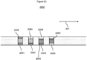
- a setup in accordance with figure 14 with 4 instead of only 2 lasers as processing beam sources, is used.
- Each 25 mm of the wire an about 7 mm long segment of the wire is processed by completely laser-ablating the Ag/AgCl-layer from circumferentially around the wire.
- 4 Nd:YVO 4 -lasers each having a peak output wavelength at 532 nm, are used as processing beam sources.
- the preceding output wavelength is obtained by frequency doubling the lasing wavelength of about 1064 nm of the Nd:YVO 4 -crystal.
- the laser is pulsed at a frequency of 160 kHz, wherein each pulse has an energy of 5 ⁇ J and a duration (width) of about 60 ns.
- the laser beam is focussed down to a focal beam diameter of 15 ⁇ m on the wire surface.
- Each laser pulse has a fluence of 2.8 J/cm 2 .
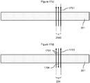
- processing of each of the 4 sections of each segment is effected by scanning the laser focus over the respective section in form of a multitude of lines/sweeps as shown in figure 17a ).
- the lines of each multitude are uni-directional and parallel to the length of the wire.
- this scanning is repeated 4 times, i.e. each section is scanned in 5 passes by the respective laser.
- the scanning speed of the laser is about 1250 mm/s.
- the distance between the lines/sweeps (pitch) is about 13 ⁇ m.
- the 4 sections of different segments which are processed in the same processing step are processed one after the other (sequentially).
- Example 2 is conducted as example 1, however, the processing of the 4 sections of different segments which are processed in the same processing step is conducted at the same time (simultaneously). Hence, the 4 lasers ablate at the same time in each of the processing steps.
- the Ag/AgCl-layer is ablated in segments of the wire as described in example 1, except for the following differences.
- the 4 lasers are not positioned to provide their focal spots to 4 different longitudinal positions of the wire. Instead, all 4 lasers are arranged to irradiate the same longitudinal position (segment) of the wire, however, each at another circumferential region (section). Further, the processing is not conducted in accordance with the figures 7 to 11d ). Instead, the segments of the wire are processed one after the other. Hence, in each processing step, exactly 1 segment is ablated. This is effected, by activating the 4 lasers one after the other.
- the first laser ablates the first section of the single segment to be processed in this process step, subsequently the second laser ablates the second section of the same segment, subsequently the third laser ablates the third section of the same segment, and subsequently the fourth laser ablates the fourth section of the same segment.
- the wire is shifted by 25 mm and the next processing step is conducted at the next segment.
- a delay is incorporated between the consecutive laser ablation actions in the same processing step. The delay is selected to allow for sufficient dissipation of the heat introduced by the previous laser action in order not to overheat the wire and, thus, damage parts of the wire other than the Ag/AgCl-layer.
- Comparative example 2 is conducted as comparative example 1, however, without the delay between consecutive laser ablation actions in the same processing step. Instead, the ablation steps are conducted directly one after the other.
- Comparative example 3 is conducted as comparative example 1 with the following exception.
- the 4 lasers ablate the Ag/AgCl-layer from the 4 sections of the same segment simultaneously.
- the Ag/AgCl-layer is removed from each segment by simultaneously irradiating the segment from all 4 sides circumferentially around the wire.
- the above described methods of processing the wires are assessed in terms of their overall process step. i.e. in terms of the time which is needed to process the whole wire.
- the processed segments of the wires are studied under an optical microscope for damages to the PU-layer which has been laid open. Any changes to the layer surface, such as molten regions or structures introduced to the surface of the PU-layer, are rated as disadvantageous.
- a wire precursor which has been prepared as described above, but without application of the Ag/AgCl-layer is used as a reference without damages to the PU-layer.
- the above trade-off is between high production rates and high accuracies of electrochemical sensors.
- This trade-off is resolved in the inventive examples 1 and 2.
- the process according to the invention allows to produce wires for high accuracy electrochemical sensors at a high production rate.
- FIG 1 shows a flow-chart of a process 100 for preparing a processed filament 410 according to the invention.
- This process 100 comprises a process step a) 101 of providing a filament 201, which comprises a multitude of segments 204, which follow one another in a longitudinal direction 401 of the filament 201. Each of these segments 204 consists a first section 202 and a second section 203, which are disposed circumferentially around the filament 201.
- the preceding definitions are illustrated by figure 2a) and 2b ).
- the filament 201 is processed in a first processing step 103 and a second processing step 104. Thereby the processed filament 410 is obtained.
- the processing steps 103, 104 are defined further in the context of figures 3) to 6b ).
- Figure 2a shows a cross-section through a filament 201 to be processed by the process 100 of figure 1 .
- the cross-section has been made through one of the segments 204 of the filament 201.
- the first section 202 and the second section 203 of this segment 204 are depicted by a full and a dashed line, respectively.
- Figure 2b shows the filament 201 of figure 2a ) in side view.
- FIG 3 shows a scheme for illustration of the processing steps 103, 104 of the process 100 of figure 1 .
- each of the processing steps 103, 104 includes processing the second section 203 of one of the segments 204 and processing the first section 202 of a neighbouring segment 204, which follows the other segment 204 in the longitudinal direction 401 of the filament 201.
- processing a section 202, 203 means irradiating this section 202, 203 with a processing beam 301 which is a laser beam for laser ablation.
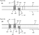
- Figure 4a shows a scheme for illustration of the first processing step 103 of the process 100 of figure 1 .
- the filament 201 in a side view.
- a first segment 402, a second segment 403 and a third segment 404 of the filament 201 are depicted. Those segments follow one another equidistantly in the longitudinal direction 401.
- a processing beam 301 processes a second section 406 of the first segment 402
- another processing beam 301 processes a first section 407 of the second segment 403.
- a first section 405 of the first segment 402 has already been processed before the first processing step 103.
- the third segment 404 is not processed in the first processing step 103.
- Figure 4b shows scheme for illustration of the second processing step 104 of the process 100 of figure 1 .
- the filament 201 has been shifted opposite to the longitudinal direction 401 by a distance between 2 neighbouring segments of the first through third segments 402 to 404.
- a processing beam 301 processes a second section 408 of the second segment 403, whereas another processing beam 301 processes a first section 409 of the third segment 404.
- the processed filament 410 is obtained.
- Figure 5a shows a cross-section through the second segment 403 of the filament 201 after the first processing step 103 of the process 100 of figure 1 .
- the first section 407 of the second segment 403 has just been processed. This is indicated by a full line which depicts the processed first section 407 in the figure.
- Figure 5b shows a cross-section through the second segment 403 of the processed filament 410 after the second processing step 104 of the process 100 of figure 1 .
- FIG 5a shows a cross-section through the second segment 403 of the processed filament 410 after the second processing step 104 of the process 100 of figure 1 .
- the second section 408 dashed line
- Figure 6a shows a side view of the second segment 403 of the filament 201 after the first processing step 103 of the process 100 of figure 1 .
- Figure 6a shows the situation of figure 5a ) in the side view.
- Figure 6b shows a side view of the second segment 403 of the processed filament 410 after the second processing step 104 of the process 100 of figure 1 .
- Figure 6b shows the situation of figure 5b ) in the side view.
- FIG. 7 shows a flow-chart of a further process 100 for preparing a processed filament 410 according to the invention.
- This process 100 comprises a process step a) 101 of providing a filament 201, which comprises a multitude of segments 204, which follow one another equidistantly in a longitudinal direction 401 of the filament 201. Each of these segments 204 consists a first section 202, a second section 203, a third section 801 and a fourth section 802, which are disposed circumferentially around the filament 201.
- the preceding definitions are illustrated by figure 8a) and 8b ).
- the filament 201 is processed in a sequence of first 103 through fourth processing steps 702. Thereby the processed filament 410 is obtained.
- the processing steps 103, 104 are defined further in the context of figures 9 to 11d ).
- Figure 8a shows a cross-section through a filament 201 to be processed by the process 100 of figure 7 .
- the cross-section has been made through one of the segments 204 of the filament 201.
- the first section 202, the second section 203, the third section 801 and the fourth section 802 of this segment 204 are depicted by different lines.
- Figure 8b shows the filament 201 of figure 8a ) in side view.
- the first section 202 cannot be seen as it is at the backside of the filament 201.
- FIG 9 shows a scheme for illustration of the first 103 through fourth processing steps 702 of the process 100 of figure 1 .
- each of the processing steps 103, 104, 701, 702 includes processing the fourth section 802 of one of the segments 204, processing the third section 801 of the next neighbouring segment 204, which follows the other segment 204 in the longitudinal direction 401 of the filament 201, processing the second section 203 of the next neighbouring segment 204 and processing the first section 202 (at the backside of the filament 201 in the figure) of the next neighbouring segment 204.
- processing a section means irradiating this section with a processing beam 301 which is a laser beam for laser ablation.
- the filament is shifted in the longitudinal direction 401 (to the left in the figure) by a distance between neighbouring segments.
- the processing beams 301 are then provided at the same place in the reference space. This is similar to what is shown in figures 4a) and 4b ) for the two processing steps of the process of figure 1 , but extended to 4 sections per segment and 4 processing steps.
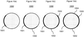
- Figure 10a shows a cross-section through the fourth segment 1000 of the filament 201 after the first processing step 103 of the process 100 of figure 7 .
- the first section 1001 of the fourth segment 1000 has just been processed. This is indicated by a full line which depicts the processed first section 1001 in the figure.
- Figure 10b shows a cross-section through the 20fourth segment 1000 of the filament 201 after the second processing step 104 of the process 100 of figure 7 .
- the first section 1001 and the second section 1002 of the 20fourth segment 1000 have already been processed. This is indicated by the different bold lines in the figure.
- Figure 10c shows a cross-section through the 20fourth segment 1000 of the filament 201 after the third processing step 701 of the process 100 of figure 7 .
- the first section 1001, the second section 1002 and the third section 1003 of the 20fourth segment 1000 have already been processed. This is indicated by the different bold lines in the figure.
- Figure 10d shows a cross-section through the second segment of the processed filament 410 after the fourth processing step 702 of the process 100 of figure 7 .
- the first section 1001, the second section 1002, the third section 1003 and the fourth section 1004 of the 20fourth segment 1000 have already been processed. This is indicated by the different bold lines in the figure.
- Figure 11a shows a side view of the 20fourth segment 1000 of the filament 201 after the first processing step 103 of the process 100 of figure 7 .
- Figure 11a shows the situation of figure 10a ) in the side view.
- Figure 11b shows a side view of the 20fourth segment 1000 of the filament 201 after the second processing step 104 of the process 100 of figure 7 .
- Figure 11b shows the situation of figure 10b ) in the side view.
- Figure 11c shows a side view of the 20fourth segment 1000 of the filament 201 after the third processing step 701 of the process 100 of figure 7 .
- Figure 11c shows the situation of figure 10c ) in the side view.
- Figure 11d shows a side view of the 20fourth segment 1000 of the processed filament 410 after the fourth processing step 702 of the process 100 of figure 1 .
- Figure 11d shows the situation of figure 10d ) in the side view.
- Figure 12 shows a cross-section through the fourth segment 1000 of the filament 201 prior to the first processing step 103 of the process 100 of figure 7 .
- a structure of the filament 201 is shown. As all the cross-sections of the figures, this one has been made with perpendicular orientation to a length of the filament 201. Over its entire length of 3 km, the filament 201 consists inside-out of a core 121, which is made from platinum; a first layer 1202, which is coated onto the core 1201 and made from a polyurethane; and a second layer 1203 which is coated onto the first layer 1202 and consists of a mixture of silver and AgCl.
- the filament 201 has an overall diameter of 200 ⁇ m.
- the filament 201 is a wire.
- the core 1201, the first layer 1202 and the second layer 1203 are co-axial to one another.
- Figure 13 shows a cross-section through the fourth segment 1000 of the processed filament 410 obtained in the fourth processing step 702 of the process 100 of figure 7 .
- the cross-section has been made through the fourth segment 1000 of the processed filament 410 and with perpendicular orientation to a length of the processed filament 410.
- Comparison to figure 12 shows that the second layer 1203 has been completely ablated from circumferentially around the segment.
- Figure 14 shows a device 1400, according to the invention, for processing a filament 201 in a process stream 1409, thereby obtaining a processed filament 410.
- the device 1400 is configured for carrying out the process 100 of figure 1 .
- the device 1400 comprises a first processing beam source 1404, which designed and arranged to emit a first processing beam onto a first section of a first segment of the filament 201 for processing the filament 201 by interaction of the first processing beam with the first section of the first segment.
- the device 1400 comprises a further processing beam source 1405, which designed and arranged to emit a further processing beam onto a further section of a further segment of the filament 201 for processing the filament 201 by interaction of the further processing beam with the further section of the further segment.
- the first segment and the further segment follow one another in a longitudinal direction 401 of the filament 201, and the first section and the further section are at different circumferential locations around the filament 201.
- the first and further processing beam sources 1404, 1405 are frequency-doubled Nd:YVO 4 -lasers.
- the device 1400 is designed for a reel-to-reel-processing of the filament 201. Accordingly, the device comprises a guiding means which, upstream of the laser, comprises a filament feed that is designed to feed the filament 201 from a feed reel 1401 which is also part of the device 1400.
- the guiding means comprises a filament take-up means which is designed for the processed filament 410 to be rolled up on a take-up reel 1408.
- the guiding means includes the take-up reel 1408.
- the guiding means further comprises a first tension control means 14002 which is designed and arranged to adapt a tension of the first an further segments of the filament 201 during the processing.
- the first tension control means 1402 comprises a first multitude of deflection rollers 1403.
- the guiding means includes a further tension control means 1406 which is arranged down-stream of the lasers.
- the further tension control means 1406, as well, is designed and arranged to adapt a tension of the first and further segments of the filament 201 during the processing.
- the further tension control means 1406 comprises a further multitude of deflection rollers 1407.
- Figure 15 shows a further device 1400, according to the invention, for processing a filament 201 in a process stream 1409, thereby obtaining a processed filament 410.
- the device 1400 of figure 15 is the same as the device 1400 of figure 14 , except for comprising only a single laser (first processing beam source 1404).
- the device of figure 15 includes a beam splitter 1501 as processing beam distribution element.
- the first processing beam source 1404 is designed and arrange to provide a first processing beam via the beam splitter 1501 onto a first section of a first segment of the filament 201 for processing the filament 201 by interaction of the first processing beam with the first section of the first segment, and to provide a further processing beam via the beam splitter 1501 onto a further section of a further segment of the filament 201 for processing the filament 201 by interaction of the further processing beam with the further section of the further segment.
- Figure 16 shows an electrical device 1600 according to the invention.
- the electrical device 1600 comprises a 2 cm long part of the processed filament 410, obtained by the process 100 of figure 7 , wherein the part includes the first through fourth segments.
- the electrical device 1600 is a medical device and the part of the processed filament 410 is a component of an electrochemical sensor.
- Figure 17a shows an illustration of parallel uni-directional processing. What is shown is a part of a filament 201, comprising a segment 204. Further, linear sweeps 1701 (so-called lines) of a first multitude of linear sweeps (so-called pass) are depicted by arrows which show a sweeping direction. Here, the linear sweeps 1701 are conducted in the same direction. The linear sweeps 1701 of the first multitude of linear sweeps are oriented in parallel to a length of the filament 201, as oriented in the segment 204. Further, a distance 1702 between the linear sweeps 1701 (so-called pitch) is depicted.
- Figure 17b shows an illustration of parallel bi-directional processing. What is shown is a part of a filament 201, comprising a segment 204. Further, linear sweeps 1701 (so-called lines) of a first multitude of linear sweeps (so-called pass) are depicted by arrows which show a sweeping direction. Here, a first fraction 1703 of the linear sweeps 1701 of the first multitude of linear sweeps is conducted in a first direction, wherein a further fraction 1704 of the linear sweeps 1701 of the first multitude of linear sweeps is conducted in a further direction, which is opposite to the first direction. The linear sweeps 1701 of the first multitude of linear sweeps are oriented in parallel to a length of the filament 201, as oriented in the segment 204. Further, a distance between the linear sweeps 1702 (so-called pitch) is depicted.
- pitch a distance between the linear sweeps 1702
- Figure 17c shows an illustration of perpendicular uni-directional processing. What is shown is a part of a filament 201, comprising a segment 204. Further, linear sweeps 1701 (so-called lines) of a first multitude of linear sweeps (so-called pass) are depicted by arrows which show a sweeping direction. Here, the linear sweeps 1701 are conducted in the same direction. The linear sweeps 1701 of the first multitude of linear sweeps are oriented perpendicular to a length of the filament 201, as oriented in the segment 204.
- Figure 17d shows an illustration of perpendicular bi-directional processing. What is shown is a part of a filament 201, comprising a segment 204. Further, linear sweeps 1701 (so-called lines) of a first multitude of linear sweeps (so-called pass) are depicted by arrows which show a sweeping direction. Here, a first fraction 1703 of the linear sweeps 1701 of the first multitude of linear sweeps is conducted in a first direction, wherein a further fraction 1704 of the linear sweeps 1701 of the first multitude of linear sweeps is conducted in a further direction, which is opposite to the first direction. The linear sweeps 1701 of the first multitude of linear sweeps are oriented in parallel to a length of the filament 201, as oriented in the segment 204.
- Figure 18 shows an optical microscope image of a processed filament 410 which is a processed wire.
- This wire is of the structure shown in figure 12 .
- a segment 204 of the wire is shown.
- the second layer 1203 has been ablated, whereas in an unprocessed section 1802 of the segment the second layer 1203 has not been removed.
- the first layer 1202 has been laid open.
- Figure 19 shows a focussed-ion-beam image of a cross-section of a wire for determining a roughness of a surface 1903 of a first layer 1202 of the wire.
- a first layer 1202 which is a PU-layer
- a second layer 1203, which is an Ag/AgCl-layer This interface is at an outer lateral surface 1903 of the first layer 1202.
- a circle 1901 has been drawn into the image as described above in the test methods section. Further, a distance 1902 between the circle 1901 and the surface 1903 of the first layer 1202 is depicted at equidistant positions along the circle 1101.
- Figure 20 shows a side view of a filament 2000 according to the invention.
- This filament 2000 is of the structure shown in figure 12 .
- the filament 2000 comprises 4 segments 2001 to 2004 which follow one another in a longitudinal direction 401 of the filament 2000.
- Each segment 2001 to 2004 cosists of 4 sections which are disposed circumferentially around the filament 2000.
- the first segment 2001 comprises exactly 4 sections 2005 which have been processed segment. One of these is in the backside of the filament 2000 in the figure.
- the second segment 2002 comprises exactly 3 sections 2005 which have been processed (one on the backside).
- the third segment 2003 comprises exactly 2 sections 2005 which have been processed (one on the backside depicted by dashed lines).
- the fourth segment 2004 comprises exactly 1 section 2005 which has been processed.
- This section 2005 is on the backside of the filament 2000 and depicted by dashed lines. Hence, from the first 2001 to the fourth segment 2004, the segments comprise an increasing number of sections 2006 which have not been processed. From each section 2005 that has been processed the second layer 1203 of the wire has been removed by laser ablation.
Landscapes
- Engineering & Computer Science (AREA)
- Physics & Mathematics (AREA)
- Optics & Photonics (AREA)
- Plasma & Fusion (AREA)
- Mechanical Engineering (AREA)
- Laser Beam Processing (AREA)
- Yarns And Mechanical Finishing Of Yarns Or Ropes (AREA)
Abstract
a) providing a filament (201), which comprises a multitude of segments (204), which follow one another in a longitudinal direction (401) of the filament (201), wherein each of the segments (204) of the multitude of segments (204) comprises a multitude of sections (202, 203), which are disposed circumferentially around the filament (201); and
b) processing the filament (201) in n processing steps 103, 104, 701, 702), thereby obtaining the processed filament (410);
wherein for each integer i in the range from 1 to n, the ith processing step comprises, for each integer j in the range from 1 to m, processing the jth section of the (i+j-1)th segment; wherein n and m are integers which are, independent from one another, at least 2; wherein sections (202, 203) of different number are at different circumferential locations of the filament (201); wherein the processing of each section (202, 203) of each segment (204) of the filament (201) comprises an interaction of the section (202, 203) of the segment (204) of the filament (201) with at least one processing beam (301). Further, the invention refers to a processed filament (410), obtainable by the process (100); to an electrical device (1600), comprising at least a part of the processed filament (410); to devices (1400) for preparing a processed filament (410); to a use of at least one laser; and to a use of a filament (201) for being processed.
Description
- The invention relates to a process for preparing a processed filament, the process comprising as process steps
- a) providing a filament, which comprises a multitude of segments, which follow one another in a longitudinal direction of the filament,
wherein each of the segments of the multitude of segments comprises a multitude of sections, which are disposed circumferentially around the filament (203); and - b) processing the filament in n processing steps, thereby obtaining the processed filament;
- Thin multilayer wires are used in applications such as electrochemical sensors. Such wires often include a metal core, a polymer coating and an outer metal coating. Preparing the wire for manufacture of an electrochemical sensor includes removal of the outer metal layer across defined segments of the wire which are then coated with enzymes. In the prior art, removal of the outer metal layer by high-precision laser ablation is known. Therein, the longitudinal positions of the wire (segments) are ablated one after the other (sequentially). This is done because the laser introduces a considerable amount of heat to the wire. Overheating of the wire may, however, damage parts of the wire which are not meant to be altered by the ablation process.
- Such damages may affect the quality of the electrochemical sensor which includes such a wire. Accordingly, such damages have to be avoided. Nevertheless, there is a strong need for higher production rates. In result, there is room for improvement of laser ablation processes of the prior art.
- From the results of the comparative examples 1 to 3, it can be seen that there is a trade-off between high process speed, i.e. high production rate, and the goal to avoid damages to the PU-layer, i.e. a high quality of processed wires. Here, it should be considered that damaging the PU-layer means to partially structure the outer surface of the PU-layer. In result, a surface tension of the outer surface of the PU-layer is not uniform across the exposed region of the PU-layer. In preparing an electrochemical sensor, this may lead to non-uniform coating thicknesses of enzyme layers on the wire. The signal-to-noise ratio of the sensor as well as the linearity of the sensor response may suffer in result. Hence, in the technical field of the invention, the above trade-off is between high production rates and high accuracies of electrochemical sensors. This trade-off is resolved in the inventive examples 1 and 2. Hence, the process according to the invention allows to produce wires for high accuracy electrochemical sensors at a high production rate.
- Generally, it is an object of the present invention to at least partly overcome a disadvantage arising from the prior art.
- It is a further object of the invention to provide a process and/or device for preparing a multilayer wire for manufacturing an electrochemical sensor of as high as possible accuracy at an as high as possible production rate.
- Therein, the sensor accuracy, preferably, refers to a signal-to-noise-ratio of the sensor or a linearity of a sensor response or both. Further, it is an object of the invention to provide a process and/or device for preparing a multilayer wire for manufacturing an electrochemical sensor, wherein a polymer layer of the wire or a metal core of the wire or both is as far as possible not damaged in the course of preparing the wire. According to a further object of the invention, one of the above advantageous processes and/or devices is provided, wherein the process/device is as simple as possible. It is a further object of the invention to provide a thin multilayer wire which is particularly suitable for manufacturing an electrochemical sensor of as high as possible accuracy, wherein the wire is obtainable at an as high as possible production rate.
- A contribution to at least one of the above objects is given by the independent claims. The dependent claims provide preferred embodiments of the present invention which also serve solving at least one of the above mentioned objects.
- A contribution to the solution of at least one of the above objects is provided by an embodiment 1 of a process, according to the invention, for preparing a processed filament, the process comprising as process steps
- a) providing a filament, which comprises a multitude of segments, which follow one another in a longitudinal direction of the filament, wherein each of the segments of the multitude of segments comprises a multitude of sections, which are disposed circumferentially around the filament; and
- b) processing the filament in n processing steps, thereby obtaining the processed filament;
- Herein, n and m are indices which are independent from one another. n defines the number of processing which are described by the above. The inventive process may, however, comprise further processing steps, i.e. more than n processing steps. m defines the number sections per segment which is processed in the n processing steps as described above. i is a running variable which runs from 1 to n. Accordingly, i is used to denote single processing steps of the n processing steps. j is a running variable which, for each of the n processing steps, runs from 1 to m. j is used to denote single sections of a segment and also to denote the respective segment. Accordingly, the characters "n", "m", "i" and "j" are not abbreviations and do not have any meaning other than being characters to identify the respective index or running variable. The sections of a segment may or may not follow one another around the circumference of the segment in the order of their numbers. The segments of the filament may or may not follow one another in the longitudinal direction of the filament in the order of their numbers. Preferably, the segments of the filament do follow one another in the longitudinal direction of the filament in the order of their numbers.
- Herein, process steps which follow one another in the order of the characters denoting the steps may follow one another directly or indirectly in time, i.e. there may be a further process step in-between or not. Further, the process steps, which follow one another in the order of the characters denoting the steps, may be conducted one after the other, in partial temporal overlap or simultaneously. Preferably, the processing steps are conducted one after the other in the order of their numbers. Herein, the term multitude means that there are at least two items which form the multitude of items. Further, herein subsequent items may follow one another directly or indirectly. Consecutive items, on the other hand, mandatorily follow one another directly. In case of items following one another directly, there is no such item in-between. There may, however, be items of another kind in-between. For example, 2 segments may follow one another directly. This means that there is no segment of the multitude of segments in-between. This does, however, not imply that the 2 segments adjoin one another.
- The process, preferably, further comprises creating an image, preferably a sequence of images, of a segment that has been processed, preferably at m sections, in the process step b). This may be conducted in the process step b) or after the process step b). Preferably, the image, preferably the sequence of images, of the segment is captured.
- In its embodiment 2, the inventive process is configured according to its embodiment 1, wherein, in each ith processing step, the processing of the 1st to mth sections is conducted at least in temporal overlap, preferably simultaneously, with one another. Here, the m sections, which are processed in each of the n processing steps, are processed in temporal overlap or, preferably, simultaneously. Accordingly, there is more than 1 processing beam, preferably m processing beams. Preferably, there are m processing beams. Preferably, there is at least one processing beam per each segment which is processed in a single processing step.
- In its embodiment 3, the inventive process is configured according to its embodiment 1 or 2, wherein n equals m.
- In its embodiment 4, the inventive process is configured according to any of its preceding embodiments, wherein the sum of the surface areas of the sections of a segment, which are processed in the process step b), equals the surface area of an outer surface of this segment. Preferably, for each segment of the multitude of segments, all the sections of the segment are equidistantly disposed around the circumference of the respective segment in terms of an angular distance between neighbouring sections along the circumference. Preferably, the surface areas of m sections of each of the segments of the multitude of segments, for each of these segments, sum up the surface area of an outer surface of the respective segment. Additionally or alternatively preferred, for each of the segments of the multitude of segments, m sections cover the whole circumference of the respective segment. Additionally or alternatively preferred, for each of the segments of the multitude of segments, the m sections are of equal circumferential span. In other words, it is preferred that each of the segments of the multitude of segments consists of m sections, wherein each of these sections covers 360°/m of a circumference of the respective segment. Additionally or alternatively preferred, for each segment of the multitude of segments, all the sections of the segment are adjacent to one another. Preferably, for each segment of the multitude of segments, all the sections of the segment are equidistantly disposed around the circumference of the respective segment in terms of an angular distance between neighbouring sections along the circumference.
- In its embodiment 5, the inventive process is configured according to any of its preceding embodiments, wherein n or m or each of both is at least 3, preferably at least 4, more preferably exactly 4. In some cases, n or m or each of both may even be more than 4. In a particularly preferred embodiment m and n are each exactly 4.
- In its embodiment 6, the inventive process is configured according to any of its preceding embodiments, wherein the segments of the multitude of segments are disposed equidistantly to one another along a length of the filament.
- In its
embodiment 7, the inventive process is configured according to any of its preceding embodiments, wherein between each of two consecutive processing steps the filament is moved in a direction of its length. Preferably, the filament is moved by a distance which is a distance between neighbouring segments of the multitude of segments. Therein, the distance is, preferably, measure in a centre-to-centre manner. A preferred kind of moving is a shifting. - In its embodiment 8, the inventive process is configured according to any of its preceding embodiments, wherein the at least one processing beam is at least one beam of particles or at least one beam of electromagnetic radiation or at least one beam of both. In the latter case, there may be at least one beam of particles and at least one beam of electromagnetic radiation, or at least one beam which is a combination of a beam of particles and a beam of electromagnetic radiation. A beam of particles may, for example, be a beam of electrons or a beam of ions or both, for example a plasma beam. Preferred electromagnetic radiation of a beam of electromagnetic radiation has a spectrum with a peak wavelength in the range from 430 to 780 nm, preferably from 430 to 640 nm, more preferably from 430 to 600 nm, more preferably from 490 to 600 nm, more preferably from 490 to 570 nm, more preferably from 500 to 560 nm, more preferably from 510 to 550 nm, more preferably from 520 to 540 nm, even more preferably from 525 to 540 nm, most preferably from 528 to 536 nm.
- In its embodiment 9, the inventive process is configured according to any of its preceding embodiments, wherein the filament comprises
- a. a core, comprising a first metal,
- b. a first layer which
- i. is superimposed on the core, and
- ii. comprises a polymer, and
- c. a second layer which
- i. is superimposed on the first layer, and
- ii. comprises a second metal.
- In its embodiment 10, the inventive process is configured according to its embodiment 9, wherein the second metal is different from the first metal.
- In its embodiment 11, the inventive process is configured according to its embodiment 9 or 10, wherein the first metal is one selected from the group consisting of platinum, tantalum, and palladium, or an alloy comprising one of the preceding metals. A preferred alloy comprising platinum is platinum iridium or platinum tungsten. A preferred alloy comprising tantalum is tantalum niobium or tantalum tungsten.
- In its embodiment 12, the inventive process is configured according to any of its embodiments 9 to 11, wherein the second metal is silver. Preferably, the second layer further comprises a salt of the second metal. A preferred salt of silver is AgCl.
- In its embodiment 13, the inventive process is configured according to any of its embodiments 9 to 12, wherein the polymer is one selected from the group consisting of a poly-addition product, a poly-condensation product, and one or more polysiloxanes, or a combination of at least two thereof. A preferred poly-addition product is polyurethane or a polyolefin. A preferred poly-condensation product is one selected from the group consisting of polyimide, polyamide, and polyethylene terephthalate, or a combination of at least two thereof. A preferred polyolefin is polyethylene or polypropylene. A further preferred polymer is a thermoplastic polymer. A particularly preferred polymer is polyurethane.
- In its embodiment 14, the inventive process is configured according to any of its preceding embodiments, wherein the processing in the processing steps is a, preferably exclusively, subtractive process, as opposed to an additive process, such as welding.
- In its embodiment 15, the inventive process is configured according to any of its embodiments 9 to 14, wherein the processing in the processing steps comprises at least partially, preferably completely, removing the second layer from the sections of the segments of the multitude of segments.
- In its embodiment 16, the inventive process is configured according to its embodiment 15, wherein, in the processing steps, at least partially, preferably completely, removing the second layer comprises ablation. Ablation is removal of material from the surface of an object by vaporisation, chipping, or other erosive processes. A preferred ablation is laser-ablation.
- In its embodiment 17, the inventive process is configured according to any of its preceding embodiments, wherein the filament has a length in range from 10 m to 10 km, preferably from 100 to 8 km, more preferably from 500 m to 5 km.
- In its embodiment 18, the inventive process is configured according to any of its preceding embodiments, wherein the filament has a diameter in the range from 0.1 to 1.0 mm, preferably from 0.1 to 0.8 mm, more preferably from 0.1 to 0.6 mm, most preferably from 0.12 to 0.4 mm.
- In its embodiment 19, the inventive process is configured according to any of its preceding embodiments, wherein the filament is one selected from the group consisting of a wire, a cable, and a fibre, or a combination of at least two thereof. A preferred fibre is an optical fibre. A particularly preferred filament is a wire.
- In its embodiment 20, the inventive process is configured according to any of its embodiments 9 to 19, wherein a thickness of the second layer is in the range from 1 to 25 µm, preferably from 2 to 20 µm, more preferably from 3 to 17 µm, most preferably from 5 to 15 µm.
- In its embodiment 21, the inventive process is configured according to any of its preceding embodiments, wherein the at least one processing beam is at least one laser beam. The at least one laser beam, preferably, has a spectrum with a peak wavelength in the range from 430 to 780 nm, preferably from 430 to 640 nm, more preferably from 430 to 600 nm, more preferably from 490 to 600 nm, more preferably from 490 to 570 nm, more preferably from 500 to 560 nm, more preferably from 510 to 550 nm, more preferably from 520 to 540 nm, even more preferably from 525 to 540 nm, most preferably from 528 to 536 nm.
- In its embodiment 22, the inventive process is configured according to its embodiment 21, wherein the at least one laser beam is at least one pulsed laser beam, as opposed to at least one continuous layer beam.
- In its embodiment 23, the inventive process is configured according to its embodiment 22, wherein the at least one pulsed laser beam is characterised by a pulse duration in a range from 10 fs to 500 ns, preferably from 50 fs to 400 ns, more preferably from 100 fs to 300 ns, more preferably from 500 fs to 200 ns, more preferably from 1 to 100 ns, even more preferably from 10 to 100 ns, most preferably from 15 to 80 ns.
- In its embodiment 24, the inventive process is configured according to its embodiment 22 or 23, wherein a fluence of the at least one pulsed laser beam is in the range from 1.0 to 5.0 J/cm2 per pulse, preferably from 1.5 to 4.5 J/cm2 per pulse, more preferably from 2.0 to 4.0 J/cm2 per pulse, most preferably from 2.5 to 3.8 J/cm2 per pulse.
- In its embodiment 25, the inventive process is configured according to any of its preceding embodiments, wherein the processing in the processing steps comprises moving at least one spot of the at least one processing beam across the section of the segment.
- In its embodiment 26, the inventive process is configured according to its embodiment 25, wherein the at least one spot is of a size in the range from 5 to 50 µm, more preferably 5 to 40 µm, most preferably 5 to 30 µm, more preferably 10 to 20 µm. A preferred spot is a focal spot. Further preferably, the sport is about circular.
- In its embodiment 27, the inventive process is configured according to any of its embodiments 22 to 26, wherein the at least one pulsed laser beam is characterised by an energy per pulse in the range from 2 to 15 µJ, preferably from 2 to 13 µJ, more preferably from 3 to 10 µJ, most preferably from 4 to 8 µJ.
- In its embodiment 28, the inventive process is configured according to any of its embodiments 22 to 27, wherein the at least one pulsed laser beam is pulsed at a frequency in the range from 5 to 600 kHz, preferably from 10 to 500 kHz, more preferably from 20 to 500 kHz, more preferably from 30 to 450 kHz, more preferably from 40 to 400 kHz, more preferably from 50 to 350 kHz, more preferably from 80 to 300 kHz, more preferably from 90 to 250 kHz, more preferably from 100 to 200 kHz, most preferably from 110 to 190 kHz.
- In its embodiment 29, the inventive process is configured according to any of its embodiments 21 to 28, wherein the at least one laser beam is obtainable from, preferably emitted by, at least one solid-state laser. A gain medium of the at least one solid-state laser is, preferably, a crystal. A preferred crystal is doped with neodym. A preferred neodym-doped crystal comprises yttrium. A preferred crystal which comprises yttrium is selected from the group consisting of Nd:YAG, Nd:Y3Al5,O12, and Nd:YVO4. Therein, Nd:YVO4 is particularly preferred.
- In its embodiment 30, the inventive process is configured according to any of its preceding embodiments, wherein, in each ith processing step, the processing of the 1st to mth sections comprises sweeping a spot of the at least one processing beam across a surface of each of the 1st to mth sections, in each case in a multitude of linear sweeps. The spot of the at least one processing beam is, preferably, a focal spot of this at least one processing beam. In case of more than one processing beam, there may be more than one spot. In this embodiment, the spot is moved across the surface of the section in a sequence of straight lines (multitude of linear sweeps), thereby scanning the surface with the at least one processing beam. Hence, each linear sweep represents a straight line. Here, the surface of the section is, preferably, an outer surface of the second layer. The surface is, preferably, an entire outer surface of the section.
- In its embodiment 31, the inventive process is configured according to its embodiment 30, wherein for each multitude of linear sweeps, the linear sweeps of this multitude of linear sweeps are conducted in the same direction. This case is also referred to as uni-directional processing.
- In its embodiment 32, the inventive process is configured according to its embodiment 30, wherein a first fraction of the linear sweeps of at least one of the multitudes of linear sweeps is conducted in a first direction, wherein a further fraction of the linear sweeps of this multitude of linear sweeps is conducted in a further direction, wherein the further direction is opposite to the first direction. This case is also referred to as bi-directional processing.
- In its embodiment 33, the inventive process is configured according to any its embodiments 30 to 32, wherein the linear sweeps of at least one of the multitudes of linear sweeps incline angles with a length of the filament in the range from 0 to 30°, preferably from 0 to 20°, more preferably from 0 to 10°, even more preferably from 0 to 5°. Most preferably the linear sweeps of the multitude of linear sweeps are parallel to the length of the filament, as oriented in the segment to be processed.
- In its embodiment 34, the inventive process is configured according to any its embodiments 30 to 33, wherein the linear sweeps of at least one of the multitudes of linear sweeps incline angles with a length of the filament in the range from 60 to 90°, preferably from 70 to 90°, more preferably from 80 to 90°, even more preferably from 85 to 90°. Most preferably the linear sweeps of the multitude of linear sweeps are perpendicular to the length of the filament, as oriented in the segment to be processed.
- In its embodiment 35, the inventive process is configured according to any its embodiments 30 to 34, wherein a distance between the linear sweeps of at least one of the multitudes of linear sweeps is in the range from 5 to 50 µm, preferably from 5 to 40 µm, more preferably from 5 to 30 µm, more preferably from 8 to 20 µm, most preferably from 10 to 20 µm. This distance is determined in a centre-to-centre manner. In the technical field, this distance is often also referred to as pitch.
- In its embodiment 36, the inventive process is configured according to any its embodiments 30 to 35, wherein, in the sweeping of the processing steps, the spot moves relative to the surface of the section at a velocity in the range from 100 to 3000 mm/s, preferably from 200 to 2500 mm/s, more preferably from 400 to 2000 mm/s, more preferably from 600 to 1800 mm/s, most preferably from 800 to 1600 mm/s.
- In its embodiment 37, the inventive process is configured according to any its embodiments 30 to 36, wherein in at least one of the multitudes of linear sweeps the spot of the at least one processing beam sweeps across each position on the surface of the section at least once. Hence, in this embodiment, the respective multitude of linear sweeps covers the entire surface of the section. In other words, in this multitude of linear sweeps, the at least one processing beam scans the entire surface of the respective section.
- In its embodiment 38, the inventive process is configured according to its embodiment 37, wherein the linear sweeps of the at least one multitude of linear sweeps is repeated 1 to 15 times, preferably 1 to 10 times, more preferably 1 to 8 times, more preferably 2 to 7 times, most preferably 2 to 5 times.
- In its embodiment 39, the inventive process is configured according to any its preceding embodiments, wherein the process step b) does not include cutting the filament.
- In its embodiment 40, the inventive process is configured according to any its preceding embodiments, wherein, after the step b) the process further comprises a step of rolling up the multitude of segments of the filament on a take-up reel.
- In its embodiment 41, the inventive process is configured according to any its preceding embodiments, wherein, in the process step a), the filament is provided on a feed reel.
- In its embodiment 42, the inventive process is configured according to any its preceding embodiments, wherein the process is performed as a reel-to-reel-process.
- In its embodiment 43, the inventive process is configured according to any its preceding embodiments, wherein each of the segments of the multitude of segments has a length in the range from 50 µm to 10 mm, preferably from 100 µm to 10 mm, more preferably from 1 to 10 mm, most preferably from 1 to 8 mm.
- A contribution to the solution of at least one of the above objects is provided by an embodiment 1 of a processed filament, according to the invention, obtainable by the inventive process according to any of its embodiments.
- In its embodiment 2, the inventive processed filament is configured according to its embodiment 1, wherein the processed filament comprises the multitude of segments, wherein in the sections of the segments of the multitude of segments
- a] a thickness of the second layer is less than outside the sections, or
- b] the second layer has been removed.
- A contribution to the solution of at least one of the above objects is provided by an embodiment 1 of a filament, according to the invention, wherein the filament comprises
- a. a core, comprising a first metal,
- b. a first layer which
- i. is superimposed on the core, and
- ii. comprises a polymer, and
- c. a second layer which
- i. is superimposed on the first layer, and
- ii. comprises a second metal;
- a] a thickness of the second layer is less than outside the sections which have been processed, or
- b] the second layer has been removed.
- In its embodiment 2, the inventive filament is configured according to its embodiment 1, wherein the filament is obtainable by the inventive process according to any of its embodiments. Preferably, the inventive filament is the processed filament as defined in the context of the process.
- In its respective embodiment 3, the inventive processed filament and the inventive filament is configured according to its embodiment 1 or 2, wherein the processed filament, respectively the filament has a length in range from 10 m to 10 km, preferably from 100 to 8 km, more preferably from 500 m to 5 km.
- In its respective embodiment 4, the inventive processed filament and the inventive filament is configured according to any of its embodiments 1 to 3, wherein the processed filament, respectively the filament is at least partially rolled up on a reel.
- In its respective embodiment 5, the inventive processed filament and the inventive filament is configured according to its embodiment 1 or 2, wherein the processed filament, respectively the filament has a length in range from 0.5 to 5 cm, preferably from 1 to 4 cm, more preferably from 1 to 3 cm.
- In its respective embodiment 6, the inventive processed filament and the inventive filament is configured according to any of its embodiments 1 to 5, wherein each of the segments has a length in the range from 50 µm to 10 mm, preferably from 100 µm to 10 mm, more preferably from 1 to 10 mm, most preferably from 1 to 8 mm.
- In its
respective embodiment 7, the inventive processed filament and the inventive filament is configured according to any of its embodiments 1 to 6, wherein outside the sections of the segments a thickness of the second layer is in a range from 1 to 25 µm, preferably from 2 to 20 µm, more preferably from 3 to 17 µm, most preferably from 5 to 15 µm. Preferably, in regions of the filament which have not been processed, the second layer has a thickness in one of the preceding ranges. - A contribution to the solution of at least one of the above objects is provided by an embodiment 1 of an electrical device, according to the invention, comprising at least a part of the inventive processed filament or the inventive filament, in each case according to any of its embodiments.
- In its embodiment 2, the inventive electrical device is configured according to its embodiment 1, wherein the electrical device comprises a sensor, which comprises the at least part of the processed filament. A preferred sensor is an electrochemical sensor.
- In its embodiment 3, the inventive electrical device is configured according to its embodiment 1 or 2, wherein the electrical device is a medical device. A preferred medical device is an implantable medical device.
- A contribution to the solution of at least one of the above objects is provided by an embodiment 1 of a device 1, according to the invention, for preparing a processed filament in a process stream, the device comprising, as components,
- a) a first processing beam source, which designed and arranged to emit a first processing beam onto a first segment of a filament for processing the filament by interaction of the first processing beam with the first segment; and
- b) a further processing beam source, which designed and arranged to emit a further processing beam onto a further segment of the filament for processing the filament by interaction of the further processing beam with the further segment;
- In its embodiment 2, the inventive device 1 is configured according to its embodiment 1, wherein the first processing beam source is designed and arranged to emit the first processing beam onto a first section of the first segment of the filament for processing the filament by interaction of the first processing beam with the first section of the first segment, wherein the further processing beam source is designed and arranged to emit the further processing beam onto a further section of the further segment of the filament for processing the filament by interaction of the further processing beam with the further section of the further segment, wherein the first section and the further section are at different circumferential locations around the filament. Preferably, the device comprises at least 3, more preferably at least 4, most preferably exactly 4, processing beam sources, wherein each processing beam source is designed and arranged to emit a processing beam onto a section of another segment of the filament for processing the filament by interaction of the respective processing beam with the respective section of respective segment, wherein the preceding sections are at different circumferential locations around the filament.
- In its embodiment 3, the inventive device 1 is configured according to its embodiment 1 or 2, wherein first processing beam source and the further processing beam source are designed and arranged for processing the filament by interaction of the first processing beam with the first section and of the further processing with the further section at least in temporal overlap with, preferably simultaneously to, one another. In case of more than 2 processing beam sources, it is preferred that all the processing beam sources are designed and arranged for processing the filament by interaction of the processing beams from the processing beam sources with the respective sections at least in temporal overlap with, preferably simultaneously to, one another.
- In its embodiment 4, the inventive device 1 is configured according to any of its embodiments 1 to 3, wherein the device is designed and arranged for conducting the inventive process according to any of its embodiments.
- In its embodiment 5, the inventive device 1 is configured according to its embodiment 4, wherein the device comprises the filament.
- In its embodiment 6, the inventive device 1 is configured according to its embodiment 4 or 5, wherein the device comprises n processing beam sources, or m processing beam sources, or each of both, wherein each of the processing beam sources is designed and arranged to emit a processing beam onto a different segment of the filament for processing the filament by interaction of the processing beam with this segment, wherein the different segments follow one another in the longitudinal direction of the filament.
- In its
embodiment 7, the inventive device 1 is configured according to its embodiment 6, wherein each of the processing beam sources is designed and arranged to emit its processing beam onto a section of the respective segment of the different segments of the filament for processing the filament by interaction of the processing beam with this section, wherein each of the sections is at a different circumferential location around the filament. - In its embodiment 8, the inventive device 1 is configured according to any of its preceding embodiments, wherein the first processing beam source is a first electromagnetic emitter, or a first particle emitter, or both, wherein the further processing beam source is a further electromagnetic emitter, or a further particle emitter, or both.
- In its embodiment 9, the inventive device 1 is configured according to its embodiment 8, wherein the first electromagnetic emitter is a first laser and the first processing beam is a first laser beam, wherein the further electromagnetic emitter is a further laser and the further processing beam is a further laser beam. Preferably, the first laser beam or the further laser beam or each of both is one of the at least one laser beams of any of the embodiments 21 to 43 of the process according to the invention.
- In its embodiment 10, the inventive device 1 is configured according to its embodiment 9, wherein the first laser beam or the further laser beam or each of both has a spectrum with a peak wavelength in the range from 430 to 780 nm, preferably from 430 to 640 nm, more preferably from 430 to 600 nm, more preferably from 490 to 600 nm, more preferably from 490 to 570 nm, more preferably from 500 to 560 nm, more preferably from 510 to 550 nm, more preferably from 520 to 540 nm, even more preferably from 525 to 540 nm, most preferably from 528 to 536 nm.
- In its embodiment 11, the inventive device 1 is configured according to its embodiment 9 or 10, wherein the first laser or the further laser of each of both is a solid-state laser. A gain medium of this solid-state laser is, preferably, a crystal. A preferred crystal is doped with neodym. A preferred neodym-doped crystal comprises yttrium. A preferred crystal which comprises yttrium is selected from the group consisting of Nd:YAG, Nd:Y3Al5,O12, and Nd:YVO4. Therein, Nd:YVO4 is particularly preferred.
- In its embodiment 12, the inventive device 1 is configured according to any of its preceding embodiments, wherein the device further comprises a first scanning element and a further scanning element, wherein the first scanning element is designed and arranged for sweeping the first processing beam across a surface of the first segment, preferably of the first section, wherein the further scanning element is designed and arranged for sweeping the further processing beam across a surface of the further segment, preferably of the further section.
- In its embodiment 13, the inventive device 1 is configured according to any of its preceding embodiments, wherein the filament comprises
- a. a core, comprising a first metal,
- b. a first layer which
- i. is superimposed on the core, and
- ii. comprises a polymer, and
- c. a second layer which
- i. is superimposed on the first layer, and
- ii. comprises a second metal.
- In its embodiment 14, the inventive device 1 is configured according to its embodiment 13, wherein the first processing beam source is designed and arranged to remove the second layer at least partially from the first segment, preferably from the first section, of the filament, wherein the further processing beam source is designed and arranged to remove the second layer at least partially from the further segment, preferably from the further section, of the filament.
- A contribution to the solution of at least one of the above objects is provided by an embodiment 1 of a device 2, according to the invention, for preparing a processed filament in a process stream, the device comprising as components
- a) a first processing beam source, and
- b) a processing beam distribution element,
wherein the first processing beam source is designed and arranged- a. to provide a first processing beam via the processing beam distribution element onto a first segment of a filament for processing the filament by interaction of the first processing beam with the first segment, and
- b. to provide a further processing beam via the processing beam distribution element onto a further segment of the filament for processing the filament by interaction of the further processing beam with the further segment,
- In its embodiment 2, the inventive device 2 is configured according to its embodiment 1, wherein the first processing beam source is designed and arranged
- a] to provide the first processing beam via the processing beam distribution element onto a first section of the first segment of the filament for processing the filament by interaction of the first processing beam with the first section of the first segment, and
- b] to provide the further processing beam via the processing beam distribution element onto a further section of the further segment of the filament for processing the filament by interaction of the further processing beam with the further section of the further segment,
- In its embodiment 3, the inventive device 2 is configured according to its embodiment 1 or 2, wherein first processing beam source and the processing beam distribution element are designed and arranged for processing the filament by interaction of the first processing beam with the first section and of the further processing with the further section at least in temporal overlap with, preferably simultaneously to, one another. In case of more than 2 processing beams, the first processing beam source and the processing beam distribution element are, preferably, designed and arranged for processing the filament by interaction of each processing beam with the respective section at least in temporal overlap with, preferably simultaneously to, one another.
- In its embodiment 4, the inventive device 2 is configured according to any of its preceding embodiments, wherein the processing beam distribution element is arranged in a beam path between the first processing beam source and the filament.
- In its embodiment 5, the inventive device 2 is configured according to any of its preceding embodiments, wherein the processing beam distribution element is a beam splitter, which is designed and arranged to split a source beam which has been emitted by the first processing beam source into the first processing beam and the further processing beam.
- In its embodiment 6, the inventive device 2 is configured according to its embodiment 5, wherein the device further comprises
- a} a first scanning element, which is
- i} arranged in a beam path of the first processing beam between the processing beam distribution element and the filament, and
- ii} designed and arranged for sweeping the first processing beam across a surface of the first segment, preferably of the first section; and
- b} a further scanning element, which is
- i} arranged in a beam path of the further processing beam between the processing beam distribution element and the filament, and
- ii} designed and arranged for sweeping the further processing beam across a surface of the further segment, preferably of the further section.
- In its
embodiment 7, the inventive device 2 is configured according to any of its embodiments 1 to 4, wherein the processing beam distribution element is a scanning element, which is designed and arranged for sweeping the first processing beam across a surface of the first segment, preferably of the first section, and for sweeping the further processing beam across a surface of the further segment, preferably of the further section. - In its embodiment 8, the inventive device 2 is configured according to its
embodiment 7, wherein the device further comprises a beam splitter, which is arranged in a beam path between the processing beam distribution element and the filament, and is designed and arranged to split a source beam which has been emitted by the first processing beam source into the first processing beam and the further processing beam. - In its embodiment 9, the inventive device 2 is configured according to any of its preceding embodiments, wherein the device is designed and arranged for conducting the process according to any of its embodiments.
- In its embodiment 10, the inventive device 2 is configured according to its embodiment 9, wherein the device comprises the filament.
- In its embodiment 11, the inventive device 2 is configured according to any of its preceding embodiments, wherein the first processing beam source is an electromagnetic emitter, or a particle emitter, or both.
- In its embodiment 12, the inventive device 2 is configured according to its embodiment 11, wherein the electromagnetic emitter is a laser, the first processing beam is a first laser beam, and the further processing beam is a further laser beam. Preferably, the first laser beam or the further laser beam or each of both is one of the at least one laser beams of any of the embodiments 21 to 43 of the process according to the invention.
- In its embodiment 13, the inventive device 2 is configured according to its embodiment 12, wherein the first laser beam or the further laser beam or each of both has a spectrum with a peak wavelength in the range from 430 to 780 nm, preferably from 430 to 640 nm, more preferably from 430 to 600 nm, more preferably from 490 to 600 nm, more preferably from 490 to 570 nm, more preferably from 500 to 560 nm, more preferably from 510 to 550 nm, more preferably from 520 to 540 nm, even more preferably from 525 to 540 nm, most preferably from 528 to 536 nm.
- In its embodiment 14, the inventive device 2 is configured according to its embodiment 12 or 13, wherein the first laser or the further laser of each of both is a solid-state laser. A gain medium of this solid-state laser is, preferably, a crystal. A preferred crystal is doped with neodym.
- A preferred neodym-doped crystal comprises yttrium. A preferred crystal which comprises yttrium is selected from the group consisting of Nd:YAG, Nd:Y3Al5,O12, and Nd:YVO4. Therein, Nd:YVO4 is particularly preferred.
- In its embodiment 15, the inventive device 2 is configured according to any of its preceding embodiments, wherein the filament comprises
- a. a core, comprising a first metal,
- b. a first layer which
- i. is superimposed on the core, and
- ii. comprises a polymer, and
- c. a second layer which
- i. is superimposed on the first layer, and
- ii. comprises a second metal.
- In its embodiment 16, the inventive device 2 is configured according to its embodiment 15, wherein the first processing beam source is designed and arranged to remove the second layer at least partially from the first segment, preferably from the first section, of the filament and at least partially from the further segment, preferably from the further section, of the filament.
- In its embodiment 15, the inventive device 1 is configured according to any of its embodiments, in its embodiment 17, the inventive device 2 is configured according to any of its embodiments, wherein, in each case, the device further comprises an imaging means, which designed and arranged to provide an image, preferably a sequence of images, of the first segment or the further segment or each of both of the processed filament. Accordingly, the imaging means is, preferably, arranged downstream, of the first processing beam source and more preferably also downstream of the further processing beam source. A preferred imaging means is an image capturing means. A preferred image capturing means is a camera. The image capturing means is designed and arranged for creating and recording an image, preferably a sequence of images, of the first segment or the further segment or each of both of the processed filament.
- In its embodiment 16, the inventive device 1 is configured according to any of its embodiments, in its embodiment 18, the inventive device 2 is configured according to any of its embodiments, wherein, in each case, the device is designed for a reel-to-reel-processing of the filament.
- In its embodiment 17, the inventive device 1 is configured according to any of its embodiments, in its embodiment 19, the inventive device 2 is configured according to any of its embodiments, wherein, in each case, the device further comprises a guiding means, comprising a filament feed, which is arranged upstream of the first processing beam source, and designed to feed the filament from a feed reel. Here, the guiding means may include the feed reel or not.
- In its embodiment 18, the inventive device 1 is configured according to its embodiment 17, in its embodiment 20, the inventive device 2 is configured according to its embodiment 19, wherein, in each case, the device comprises the feed reel.
- In its embodiment 19, the inventive device 1 is configured according to its embodiment 17 or 18, in its embodiment 21, the inventive device 2 is configured according to its embodiment 19 or 20, wherein, in each case, the guiding means further comprises a filament take-up means, which is arranged down-stream of the first processing beam source, preferably also down-stream of the further processing beam source. Preferably, between the filament feed and the filament take-up means, the device includes no means to cut the filament.
- In its embodiment 20, the inventive device 1 is configured according to its embodiment 19, in its embodiment 22, the inventive device 2 is configured according to its embodiment 21, wherein, in each case, the filament take-up means is designed for the processed filament to be rolled up on a take-up reel. Here, the guiding means may include the take-up reel or not.
- In its embodiment 21, the inventive device 1 is configured according to its embodiment 20, in its embodiment 23, the inventive device 2 is configured according to its embodiment 22, wherein, in each case, the device comprises the take-up reel.
- In its embodiment 22, the inventive device 1 is configured according to any of its embodiments 17 to 21, in its embodiment 24, the inventive device 2 is configured according to any of its embodiments 19 to 23, wherein, in each case, the guiding means further comprises a first tension control means which is arranged up-stream of the first processing beam source, wherein the first tension control means is designed and arranged to adapt a tension of the first segment or of the further segment or of each of both during the processing. Preferably, the first tension control means is arranged between the filament feed and the first processing beam source.
- In its embodiment 23, the inventive device 1 is configured according to its embodiment 22, in its embodiment 25, the inventive device 2 is configured according to its embodiment 24, wherein, in each case, the first tension control means comprises a first multitude of deflection rollers.
- In its embodiment 24, the inventive device 1 is configured according to any of its embodiments 17 to 23, in its embodiment 26, the inventive device 2 is configured according to any of its embodiments 19 to 25, wherein, in each case, the guiding means further comprises a further tension control means which is arranged down-stream of the first processing beam source, preferably also of the further processing beam source, wherein the further tension control means is designed and arranged to adapt a tension of the first segment or of the further segment or of each of both during the processing. Preferably, the further tension control means is arranged between the first processing beam source and the filament take-up means, more preferably between the further processing beam source and the filament take-up means.
- In its embodiment 25, the inventive device 1 is configured according to its embodiment 24, in its embodiment 27, the inventive device 2 is configured according to its embodiment 26, wherein, in each case, the further tension control means comprises a further multitude of deflection rollers.
- In its embodiment 26, the inventive device 1 is configured according to any of its embodiments 18 to 25, in its embodiment 28, the inventive device 2 is configured according to any of its embodiments 20 to 27, wherein, in each case, a first part of the filament is rolled up on the feed reel. The feed reel is, preferably, arranged up-stream of the first processing beam source. Preferably, the first segment and the further segment are down-stream of the first part.
- In its embodiment 27, the inventive device 1 is configured according to any of its embodiments 21 to 26, in its embodiment 29, the inventive device 2 is configured according to any of its embodiments 23 to 28, wherein, in each case, a further part of the filament is rolled up on the take-up reel. The take-up reel is, preferably, arranged down-stream of the first processing beam source, preferably also of the further processing beam source. Preferably, the first segment and the further segment are up-stream of the further part. Further preferred, the first segment and the further segment are between the first and the further part of the filament.
- A contribution to the solution of at least one of the above objects is provided by an embodiment 1 of a use 1, according to the invention, of at least one laser for providing the at least one processing beam in the inventive process according to any of its embodiments, or as the first processing beam source of the device 1 or 2, in each case according to any of its embodiments.
- A contribution to the solution of at least one of the above objects is provided by an embodiment 1 of a use 2, according to the invention, of a filament for being processed in the inventive process according to any of its embodiments, or by the device 1 or 2, in each case, according to any of its embodiments, in each case, thereby obtaining the processed filament from the filament. Preferably, the filament is the filament described in any of the embodiments of the process according to the invention.
- Features described as preferred in one category of the invention, such as the process or the device 1 or 2 of the invention, are likewise preferred in a respective embodiment of the further categories of the invention, including the inventive processed filament and uses.
- In the context of the invention, the filament may be any kind of filament which the skilled person deems appropriate. Herein, a filament is a linear, non-rigid element which has a length that is at least 10 times, preferably at least 100 times, more preferably at least 1000 times, a diameter of the filament. Therein, "non-rigid" means that the filament is flexible at least to a degree which allows to reversibly roll the filament up on a roll without damaging the filament. In a cross-section which is perpendicular to the length of the filament, the filament may have any shape which the skilled person deems appropriate. Preferably, the filament has a cross-sectional shape, selected from the group consisting of circular, rectangular, oval, and elliptical, wherein a circular cross-section is particularly preferred. Preferably, the filament has the preceding cross-sectional shape over its full length. A particularly preferred filament is a wire. The longitudinal direction of the filament is a direction of a length of the filament.
- Each segment of the multitude of segments is a longitudinally extending portion of the filament, wherein a length of the segment is shorter than the length of the filament. Preferably, the length of the filament is at least 100 times, preferably at least 1000 times, the length of the segment. Preferably, the segments of the multitude of segments are spaced apart from one another in the longitudinal direction. This means that, preferably, no 2 segments adjoin one another.
- A preferred filament comprises a multilayer structure. The filament, preferably, comprises the core, the first layer which superimpose the core and the second layer which superimposes the first layer. Herein, the term "superimpose" means that the entities given may follow one another directly, in case of which they are in contact with each other, or indirectly, in case of which there is at least one further entity in-between. Hence, there may or may not be further layers between the core and the first layer and/or the first layer and the second layer. Preferably, the first layer is in contact with the core. Additionally or alternatively preferred, the second layer is on contact with the first layer. In each cross-section through the filament, which is perpendicular to the length of the filament, the core, preferably, comprises a geometric centre of the filament. Further, the second layer may be superimposed by a further layer on its outer side or not. Preferably, the second layer is not superimposed by any further layer on its outer side, i.e. the side which faces away from the core. Before processing the filament, the first layer, preferably, superimposes the core over at least 50 %, more preferably at least 60 %, more preferably at least 70 %, more preferably at least 80 %, more preferably at least 90 %, most preferably 100 %, in each case of an entire lateral surface of the core. Additionally or alternatively preferred, the second layer superimposes the first layer over at least 50 %, more preferably at least 60 %, more preferably at least 70 %, more preferably at least 80 %, more preferably at least 90 %, most preferably 100 %, in each case of an entire lateral surface of the first layer, wherein this lateral surface faces away from the core. After processing the filament, the preceding holds, preferably, outside of regions of the filament that have been processed. Hence, at least the sections which have been processed are excluded from this specification. The core, preferably, is of a shape of a cylinder which may have been bend (oblique cylinder). Preferably, the first layer or the second layer or both is of the shape of a hollow cylinder, respectively. Herein, the term cylinder does not restrict a cross-sectional shape. A preferred cylinder is a circular cylinder (circular cross-sectional shape) or a prism (polygonal cross-sectional shape). The core, the first layer and the second layer may be co-axial or not. In particular, the second layer is often not co-axial to the core and the first layer.
- The core of the filament comprises the first metal, preferably, in a proportion in the range from 50 to 100 wt.-%, preferably from 60 to 100 wt.-%, more preferably from 70 to 100 wt.-%, even more preferably from 80 to 100 wt.-%, most preferably from 90 to 100 wt.-%, in each case based on the weight of the core. A preferred first metal is biocompatible. More preferably, the overall core material is biocompatible. The first layer comprises the polymer, preferably, in a proportion in the range from 50 to 100 wt.-%, preferably from 60 to 100 wt.-%, more preferably from 70 to 100 wt.-%, even more preferably from 80 to 100 wt.-%, most preferably from 90 to 100 wt.-%, in each case based on the weight of the first layer. Preferably, the polymer of the first layer, more preferably the overall material of the first layer is biocompatible. The second layer comprises the second metal, preferably, in a proportion in the range from 50 to 100 wt.-%, preferably from 60 to 100 wt.-%, more preferably from 70 to 100 wt.-%, even more preferably from 80 to 100 wt.-%, most preferably from 90 to 100 wt.-%, in each case based on the weight of the second layer. Preferably, the second metal, more preferably the overall material of the second layer is biocompatible. Preferably, each of the materials of the filament defined herein is biocompatible. A preferred filament consists essentially of biocompatible materials. A preferred biocompatible material is one selected from the group consisting of biotolerant, bioinert and bioactive or a combination of at least two thereof. Preferably, the first metal or the second metal or each of both is a noble metal. Preferably, the first and second metals are different noble metals.
- In a preferred filament, a surface of the first layer is characterised by an average roughness Ra in the range from 0.07 to 4 µm, preferably from 0.1 to 2 µm, more preferably from 0.2 to 1.2 µm; or by a root-mean-squared roughness Rq in the range from 0.2 to 7 µm, preferably from 0.5 to 4 µm, more preferably from 1 to 3.5 µm; or by each of both kinds of roughness. The preceding surface of the first layer, preferably, faces the second layer. This means that the surface is, preferably, an outer surface of the first layer. Preferably, the surface is at least part of a lateral surface of the first layer. Preferably, the surface represents 50 to 100 %, more preferably 60 to 100 %, more preferably 70 to 100 %, more preferably 80 to 100 %, more preferably 90 to 100 %, most preferably 95 to 100 %, of an overall outer lateral surface of the first layer. Preferably, a surface of the core is characterised by an average roughness which is less, preferably at least by a factor 0.1, than the average roughness Ra of the surface of the first layer; or by a root-mean-squared roughness which is less, preferably at least by a factor 0.1, than the root-mean-squared roughness Rq of the surface of the first layer; or by both of the preceding specifications. Preferably, the average roughness of the surface of the core is in the range from 0.001 to 0.1 µm, preferably from 0.005 to 0.05 µm, more preferably from 0.01 to 0.05 µm. Additionally or alternatively preferred, the root-mean-squared roughness of the surface of the core is in the range from 0.001 to 0.1 µm, preferably from 0.006 to 0.06 µm, more preferably from 0.02 to 0.06 µm. The preceding surface of the core is, preferably, at least part of a lateral surface of the core. Preferably, the surface represents 50 to 100 %, more preferably 60 to 100 %, more preferably 70 to 100 %, more preferably 80 to 100 %, more preferably 90 to 100 %, most preferably 95 to 100 %, of an overall lateral surface of the core.
- In the context of the invention, the guiding means may be any means which the skilled person deems suitable for guiding the filament such that the segment is arranged during the processing in a predetermined orientation. In general, the guiding means is one or more elements of the device 1 or 2 according to the invention which defines an orientation of a the segment during processing this segment. Further, the guiding means may define a fixation of the segment during processing or a tension of the segment during processing or both. The orientation of the segment may, for example, be achieved by an appropriate arrangement of the filament feed or the filament take-up means or both. Alternatively, the orientation of the segment during processing may be achieved by means of suitably arranged deflection rollers of the guiding means. Those deflection rollers may be part of the first and/or further tension control means.
- In the context of the invention, the processing of the filament may be any kind of processing which the skilled person deems appropriate and which can be achieved by interaction of the at least one processing beam with the section or segment of the filament. A preferred interaction is absorption. A particularly preferred processing includes removing part of the filament in the section or segment, preferably by ablation, more preferably laser-ablation.
- Reel-to-reel-processing means provision of the filament at least partially rolled up on a reel, at least partially unwinding the filament from the reel, then processing and then at least partially re-winding the processed filament on a further reel. Most preferably, the filament is not cut in that process. Here, cutting means separating the filament into at least two distinct filaments.
- In case of a non-circular shape, such as a cross-section of the filament, the diameter of the shape is a length of a longest straight line which starts and ends on the edge of the shape.
- In the context of the invention, the recited scanning elements may be any element which the skilled person deems suitable for sweeping the respective processing beam across a surface of the respective segment or section. By means of the scanning element, the processing beam can be provided to different target locations one after the other, but not simultaneously to the different target locations. The latter requires to split up the beam which can be done by a beam splitter. The scanning element is, preferably, an optical component which is designed to deflect a processing beam, preferably a laser beam. Therein, an angle of deflection can, preferably, be changed, more preferably scanned across an angular range. A preferred scanning element comprises a mirror which is designed and arranged in a movable manner. Preferably the mirror can be swiveled around an axis of rotation. A preferred scanning element is of a galvanometer type.
- The test methods which follow were utilized within the context of the invention. Unless stated otherwise, the measurements were conducted at an ambient temperature of 23 °C, an ambient air pressure of 100 kPa (0.986 atm) and a relative air humidity of 50 %.
- In order to determine the roughness of a surface of layer or of the core of the filament, a cross-section through the filament which is perpendicular to the filament length is prepared. The cross-section is polished prior to focussed-ion-beam (FIB) inspection. An FIB image is assessed using suitable image editing software. Depending on the general cross-sectional shape of the surface to be examined, a suitable geometric form is drawn. In the case of a circular filament, a circle is drawn. The diameter of the circle is chosen to match the diameter of the surface to be examined in the cross-section. The position of the circle is fitted to the surface to be examined. The distance of the surface to the circle in radial direction is measured at 10 positions equidistantly around the circumference of the circle (see
figure 19 ). The average roughness Ra is obtained by calculating the arithmetic mean of the 10 distances, whereas the root-mean-squared roughness Rq is obtained by calculating the root mean square of the 10 distances. - In case of a laser beam as processing beam, the peak wavelength of the spectrum is the nominal peak wavelength of the laser output. This is either the wavelength at which the laser lases or, if a non-linear optical process is used to alter the output wavelength, the respective harmonic of the lasing wavelength. For example, a KrF-Excimer laser typically has a lasing wavelength at about 248 nm. A Nd:YVO4-laser typically has a lasing wavelength at about 1064 nm. If the light of the Nd:YVO4-laser is frequency doubled, the peak wavelength of the laser output is at about 532 nm. If the processing beam is not a laser beam, but another type of beam of electromagnetic radiation, the spectrum of this electromagnetic radiation is measured using a spectrometer of the type CCS200 from Thorlabs GmbH. The measurement is conducted in accordance with the manufacturer's instructions. The peak wavelength of the measured spectrum is then a local maximum of the spectrum which is also its global maximum.
- The pulse Frequency is defined as the number of pulses, emitted per unit of time. The pulse frequency of a pulsed laser is adjusted at the device. Any pulse frequency, referred to herein, means the pulse frequency as adjusted at the device.
- The pulse duration is defined as the time duration between the intensity levels of a pulse measured at FWHM (full width at half-maximum). It is measured with a suitable photo diode and an oscilloscope.
- The fluence is defined as energy per pulse [J] / effective focal spot area [cm2]. Therein, the effective focal spot area is calculated as the area of a circle of a diameter which is the spot size according to the test method below.
- The energy per pulse is determined by first measuring the accumulated energy of the beam over a period of irradiation of 1 second using a thermal power meter. If the focus of the beam is on the workpiece, this energy is measured right in front of the workpiece, i.e. slightly out of the focus point. The pulse frequency is determined as described above. The energy per pulse is calculated by dividing the accumulated energy by the pulse frequency in Hz.
- The 2D-intensity distribution of the spot is measured using a 2D power meter. The spot size is determined by fitting a circle to the Full Width at half Maximum of the 2D-intensity distribution. The spot size is the diameter of this circle.
- The invention is illustrated further by way of example hereinafter by examples and figures. The invention is neither restricted to the examples nor the figures.
- In the comparative examples (not according to the invention) and the examples (according to the invention), wires which have been prepared as described below are processed as described further below.
- 3 km long wires which consist from the inside to the outside of a core of tantalum, a platinum layer, a polyurethane layer and a layer consisting of a mixture of silver and AgCl (Ag/AgCl-layer), are prepared as described in the following.
- A wire precursor consisting of a core of tantalum and a cladding of platinum is prepared. This is effected by drawing a tube made of platinum on a rod made of tantalum. Further a conventional wire drawing method is applied to the wire precursor. This includes single die drawing (elongation per die 5 to 15 %) the wire precursor at a drawing speed of about 10 m/min using lubrication oil. Ultrasonic cleaning and rinsing of the wire precursor are conducted in-line. Subsequently, an intermediate annealing step is conducted at an annealing temperature of 800 °C. Therein, the wire precursor is moved through a furnace at an annealing speed of 20 m/min. Thereby, mechanical properties of the wire precursor are adjusted. Subsequently, multi die drawing (elongation per die 10 to 20 %) is conducted at a drawing speed of 30 m/min using lubrication oil. Ultrasonic cleaning and rinsing of the wire precursor are conducted in-line. Further in-line, the wire precursor is coated with a resin of polyurethane. This is done by applying a wet film of the resin on the wire using enameling dies. Then the applied resin is dried thermally and the polymer is cured in an annealer. The applying, drying and curing steps are repeated 10 to 40 times in order to obtained a polyurethane layer thickness of about 20 µm. The polyurethane layer is coated in-line with an Ag/AgCl-layer.
- This is done by applying a paste, which includes silver particles, AgCl, binder and solvent, to the polyurethane layer by enamel dies. The applied paste is dried thermally and cured. The steps of applying, drying and curing are repeated 2 to 10 times in order to obtain a 10 µm thick Ag/AgCl. A paste with a fineness of grind (as defined in ASTM D1316) of about 12 to 5 µm (50 point) and about 12 to 20 µm (fourth continuous scratch), and a temperature of about 300 to 450 °C is used for application of the Ag/AgCl layer.
- Fineness of grind as defined in ASTM D1316 is measured by dragging a paste through a wedge using a scraping tool, from the deep end to the shallow end, and the location of the fourth continuous scratch is measured at a scale. This value corresponds to the fourth-largest particle agglomerate size in the paste. Furthermore, the so-called "50 point" is measured at the location where half of the surface of the wedge is scratched.
- In the example 1, wires which have been prepared as described above are processed in a reel-to-reel fashion. A setup in accordance with
figure 14 , however, with 4 instead of only 2 lasers as processing beam sources, is used. Each 25 mm of the wire, an about 7 mm long segment of the wire is processed by completely laser-ablating the Ag/AgCl-layer from circumferentially around the wire. Here, 4 Nd:YVO4-lasers, each having a peak output wavelength at 532 nm, are used as processing beam sources. The preceding output wavelength is obtained by frequency doubling the lasing wavelength of about 1064 nm of the Nd:YVO4-crystal. For the laser ablation, the laser is pulsed at a frequency of 160 kHz, wherein each pulse has an energy of 5 µJ and a duration (width) of about 60 ns. The laser beam is focussed down to a focal beam diameter of 15 µm on the wire surface. Each laser pulse has a fluence of 2.8 J/cm2. - The processing is conducted as described in the context of
figures 7 to 11d ). Hence, m = n = 4. The processing, however, does not stop after 4 processing steps. Instead, the processing is set forth by starting another 4 processing steps which are followed by further 4 processing steps and so forth. After each processing step, the wire is shifted by the distance between two neighbouring segments, i.e. by 25 mm. Hence, consecutive blocks of 4 processing steps overlap with one another in terms of the segments which are processed in these blocks. This way an overall continuous process is obtained which allows to completely ablate the Ag/AgCl-layer from segments each 25 mm of the wire over its entire length. - In the preceding, processing of each of the 4 sections of each segment is effected by scanning the laser focus over the respective section in form of a multitude of lines/sweeps as shown in
figure 17a ). The lines of each multitude are uni-directional and parallel to the length of the wire. Per section, this scanning is repeated 4 times, i.e. each section is scanned in 5 passes by the respective laser. Therein, the scanning speed of the laser is about 1250 mm/s. The distance between the lines/sweeps (pitch) is about 13 µm. In this particular example, the 4 sections of different segments which are processed in the same processing step are processed one after the other (sequentially). - Example 2 is conducted as example 1, however, the processing of the 4 sections of different segments which are processed in the same processing step is conducted at the same time (simultaneously). Hence, the 4 lasers ablate at the same time in each of the processing steps.
- In the comparative example 1, the Ag/AgCl-layer is ablated in segments of the wire as described in example 1, except for the following differences. The 4 lasers are not positioned to provide their focal spots to 4 different longitudinal positions of the wire. Instead, all 4 lasers are arranged to irradiate the same longitudinal position (segment) of the wire, however, each at another circumferential region (section). Further, the processing is not conducted in accordance with the
figures 7 to 11d ). Instead, the segments of the wire are processed one after the other. Hence, in each processing step, exactly 1 segment is ablated. This is effected, by activating the 4 lasers one after the other. Thus, in each of the process steps, first the first laser ablates the first section of the single segment to be processed in this process step, subsequently the second laser ablates the second section of the same segment, subsequently the third laser ablates the third section of the same segment, and subsequently the fourth laser ablates the fourth section of the same segment. This way the Ag/AgCl-layer is removed completely from the preceding segment. Subsequently, the wire is shifted by 25 mm and the next processing step is conducted at the next segment. In this particular, comparative example, a delay is incorporated between the consecutive laser ablation actions in the same processing step. The delay is selected to allow for sufficient dissipation of the heat introduced by the previous laser action in order not to overheat the wire and, thus, damage parts of the wire other than the Ag/AgCl-layer. - Comparative example 2 is conducted as comparative example 1, however, without the delay between consecutive laser ablation actions in the same processing step. Instead, the ablation steps are conducted directly one after the other.
- Comparative example 3 is conducted as comparative example 1 with the following exception. In each of the processing steps, the 4 lasers ablate the Ag/AgCl-layer from the 4 sections of the same segment simultaneously. Hence, the Ag/AgCl-layer is removed from each segment by simultaneously irradiating the segment from all 4 sides circumferentially around the wire.
- The above described methods of processing the wires are assessed in terms of their overall process step. i.e. in terms of the time which is needed to process the whole wire. After having processed the wires as described above for the comparative examples and examples, the processed segments of the wires are studied under an optical microscope for damages to the PU-layer which has been laid open. Any changes to the layer surface, such as molten regions or structures introduced to the surface of the PU-layer, are rated as disadvantageous. As a reference without damages to the PU-layer, a wire precursor which has been prepared as described above, but without application of the Ag/AgCl-layer is used.
- The results of the above studies are summarised in the below table. Therein, "--" means a result which is less favourable than "-", "-" means a result which is less favourable than "+", and "+" means a result which is less favourable than "++".
High Process Speed Avoidance of Damages to the Wire Comparative Example 1 - + Comparative Example 2 + - Comparative Example 3 ++ - Example 1 + + Example 2 ++ + - From the results of the comparative examples 1 to 3, it can be seen that there is a trade-off between high process speed, i.e. high production rate, and the goal to avoid damages to the PU-layer, i.e. a high quality of processed wires. Here, it should be considered that damaging the PU-layer means to partially structure the outer surface of the PU-layer. In result, a surface tension of the outer surface of the PU-layer is not uniform across the exposed region of the PU-layer. In preparing an electrochemical sensor, this may lead to non-uniform coating thicknesses of enzyme layers on the wire. The signal-to-noise ratio of the sensor as well as the linearity of the sensor response may suffer in result. Hence, in the technical field of the invention, the above trade-off is between high production rates and high accuracies of electrochemical sensors. This trade-off is resolved in the inventive examples 1 and 2. Hence, the process according to the invention allows to produce wires for high accuracy electrochemical sensors at a high production rate.
- The figures show, in schematic form and not to scale, unless stated otherwise in the description or the respective figure:
- Figure 1
- a flow-chart of a process according to the invention;
- Figure 2a)
- a cross-section through a filament to be processed by the process of
figure 1 , depicting the sections of a segment; - Figure 2b)
- the filament of
figure 2a ) in side view; - Figure 3
- a scheme for illustration of a general processing step of the process of
figure 1 ; - Figure 4a)
- a scheme for illustration of the first processing step of the process of
figure 1 ; - Figure 4b)
- a scheme for illustration of the second processing step of the process of
figure 1 ; - Figure 5a)
- a cross-section through the second segment of the filament after the first processing step of the process of
figure 1 ; - Figure 5b)
- a cross-section through the second segment of the processed filament after the second processing step of the process of
figure 1 ; - Figure 6a)
- a side view of the second segment of the filament after the first processing step of the process of
figure 1 ; - Figure 6b)
- a side view of the second segment of the processed filament after the second processing step of the process of
figure 1 ; - Figure 7
- a flow-chart of a further process according to the invention;
- Figure 8a)
- a cross-section through a filament to be processed by the process of
figure 7 , depicting the sections of a segment; - Figure 8b)
- the filament of
figure 8a ) in side view; - Figure 9
- a scheme for illustration of a general processing step of the process of
figure 7 ; - Figure 10a)
- a cross-section through the fourth segment of the filament after the first processing step of the process of
figure 7 ; - Figure 10b)
- a cross-section through the fourth segment of the filament after the second processing step of the process of
figure 7 ; - Figure 10c)
- a cross-section through the fourth segment of the filament after the third processing step of the process of
figure 7 ; - Figure 10d)
- a cross-section through the fourth segment of the filament after the fourth processing step of the process of
figure 7 ; - Figure 11a)
- a side view of the fourth segment of the filament after the first processing step of the process of
figure 7 ; - Figure 11b)
- a side view of the fourth segment of the filament after the second processing step of the process of
figure 7 ; - Figure 11c)
- a side view of the fourth segment of the filament after the third processing step of the process of
figure 7 ; - Figure 11d)
- a side view of the fourth segment of the filament after the fourth processing step of the process of
figure 7 ; - Figure 12
- a cross-section through a filament depicting the structure of the filament;
- Figure 13
- a cross-section through a processed filament;
- Figure 14
- a device according to the invention;
- Figure 15
- a further device according to the invention;
- Figure 16
- an electrical device according to the invention;
- Figure 17a)
- an illustration of parallel uni-directional processing;
- Figure 17b)
- an illustration of parallel bi-directional processing;
- Figure 17c)
- an illustration of perpendicular uni-directional processing;
- Figure 17d)
- an illustration of perpendicular bi-directional processing;
- Figure 18
- an optical microscope image of a processed wire;
- Figure 19
- a focussed-ion-beam image of a cross-section of a wire for determining a roughness of a surface of a first layer of the wire; and
- Figure 20
- a side view of a filament according to the invention.
-
Figure 1 shows a flow-chart of aprocess 100 for preparing a processedfilament 410 according to the invention. Thisprocess 100 comprises a process step a) 101 of providing afilament 201, which comprises a multitude ofsegments 204, which follow one another in alongitudinal direction 401 of thefilament 201. Each of thesesegments 204 consists afirst section 202 and asecond section 203, which are disposed circumferentially around thefilament 201. The preceding definitions are illustrated byfigure 2a) and 2b ). In a process step b) 102, thefilament 201 is processed in afirst processing step 103 and asecond processing step 104. Thereby the processedfilament 410 is obtained. The processing steps 103, 104 are defined further in the context offigures 3) to 6b ). -
Figure 2a ) shows a cross-section through afilament 201 to be processed by theprocess 100 offigure 1 . The cross-section has been made through one of thesegments 204 of thefilament 201. Here, thefirst section 202 and thesecond section 203 of thissegment 204 are depicted by a full and a dashed line, respectively. -
Figure 2b ) shows thefilament 201 offigure 2a ) in side view. -
Figure 3 shows a scheme for illustration of the processing steps 103, 104 of theprocess 100 offigure 1 . What is shown is that each of the processing steps 103, 104 includes processing thesecond section 203 of one of thesegments 204 and processing thefirst section 202 of a neighbouringsegment 204, which follows theother segment 204 in thelongitudinal direction 401 of thefilament 201. Therein processing asection section processing beam 301 which is a laser beam for laser ablation. -
Figure 4a ) shows a scheme for illustration of thefirst processing step 103 of theprocess 100 offigure 1 . What is shown is thefilament 201 in a side view. Afirst segment 402, asecond segment 403 and athird segment 404 of thefilament 201 are depicted. Those segments follow one another equidistantly in thelongitudinal direction 401. In thefirst processing step 103, aprocessing beam 301 processes asecond section 406 of thefirst segment 402, whereas anotherprocessing beam 301 processes afirst section 407 of thesecond segment 403. Afirst section 405 of thefirst segment 402 has already been processed before thefirst processing step 103. Thethird segment 404 is not processed in thefirst processing step 103. -
Figure 4b ) shows scheme for illustration of thesecond processing step 104 of theprocess 100 offigure 1 . Between the first 103 and second processing steps 104, thefilament 201 has been shifted opposite to thelongitudinal direction 401 by a distance between 2 neighbouring segments of the first throughthird segments 402 to 404. In thesecond processing step 104, aprocessing beam 301 processes asecond section 408 of thesecond segment 403, whereas anotherprocessing beam 301 processes afirst section 409 of thethird segment 404. Thereby, the processedfilament 410 is obtained. -
Figure 5a ) shows a cross-section through thesecond segment 403 of thefilament 201 after thefirst processing step 103 of theprocess 100 offigure 1 . In that situation, thefirst section 407 of thesecond segment 403 has just been processed. This is indicated by a full line which depicts the processedfirst section 407 in the figure. -
Figure 5b ) shows a cross-section through thesecond segment 403 of the processedfilament 410 after thesecond processing step 104 of theprocess 100 offigure 1 . With respect tofigure 5a ), not only thefirst section 407 of thesecond segment 403, but also the second section 408 (dashed line) has been processed. -
Figure 6a ) shows a side view of thesecond segment 403 of thefilament 201 after thefirst processing step 103 of theprocess 100 offigure 1 .Figure 6a ) shows the situation offigure 5a ) in the side view. -
Figure 6b ) shows a side view of thesecond segment 403 of the processedfilament 410 after thesecond processing step 104 of theprocess 100 offigure 1 .Figure 6b ) shows the situation offigure 5b ) in the side view. -
Figure 7 shows a flow-chart of afurther process 100 for preparing a processedfilament 410 according to the invention. Thisprocess 100 comprises a process step a) 101 of providing afilament 201, which comprises a multitude ofsegments 204, which follow one another equidistantly in alongitudinal direction 401 of thefilament 201. Each of thesesegments 204 consists afirst section 202, asecond section 203, athird section 801 and afourth section 802, which are disposed circumferentially around thefilament 201. The preceding definitions are illustrated byfigure 8a) and 8b ). In a process step b) 102, thefilament 201 is processed in a sequence of first 103 through fourth processing steps 702. Thereby the processedfilament 410 is obtained. The processing steps 103, 104 are defined further in the context offigures 9 to 11d ). -
Figure 8a ) shows a cross-section through afilament 201 to be processed by theprocess 100 offigure 7 . The cross-section has been made through one of thesegments 204 of thefilament 201. Here, thefirst section 202, thesecond section 203, thethird section 801 and thefourth section 802 of thissegment 204 are depicted by different lines. -
Figure 8b ) shows thefilament 201 offigure 8a ) in side view. Here, thefirst section 202 cannot be seen as it is at the backside of thefilament 201. -
Figure 9 shows a scheme for illustration of the first 103 through fourth processing steps 702 of theprocess 100 offigure 1 . What is shown is that each of the processing steps 103, 104, 701, 702 includes processing thefourth section 802 of one of thesegments 204, processing thethird section 801 of the next neighbouringsegment 204, which follows theother segment 204 in thelongitudinal direction 401 of thefilament 201, processing thesecond section 203 of the next neighbouringsegment 204 and processing the first section 202 (at the backside of thefilament 201 in the figure) of the next neighbouringsegment 204. Therein processing a section means irradiating this section with aprocessing beam 301 which is a laser beam for laser ablation. Between consecutive processing steps the filament is shifted in the longitudinal direction 401 (to the left in the figure) by a distance between neighbouring segments. The processing beams 301 are then provided at the same place in the reference space. This is similar to what is shown infigures 4a) and 4b ) for the two processing steps of the process offigure 1 , but extended to 4 sections per segment and 4 processing steps. -
Figure 10a ) shows a cross-section through thefourth segment 1000 of thefilament 201 after thefirst processing step 103 of theprocess 100 offigure 7 . In that situation, thefirst section 1001 of thefourth segment 1000 has just been processed. This is indicated by a full line which depicts the processedfirst section 1001 in the figure. -
Figure 10b ) shows a cross-section through the20fourth segment 1000 of thefilament 201 after thesecond processing step 104 of theprocess 100 offigure 7 . In that situation, thefirst section 1001 and thesecond section 1002 of the20fourth segment 1000 have already been processed. This is indicated by the different bold lines in the figure. -
Figure 10c ) shows a cross-section through the20fourth segment 1000 of thefilament 201 after thethird processing step 701 of theprocess 100 offigure 7 . In that situation, thefirst section 1001, thesecond section 1002 and thethird section 1003 of the20fourth segment 1000 have already been processed. This is indicated by the different bold lines in the figure. -
Figure 10d ) shows a cross-section through the second segment of the processedfilament 410 after thefourth processing step 702 of theprocess 100 offigure 7 . In that situation, thefirst section 1001, thesecond section 1002, thethird section 1003 and thefourth section 1004 of the20fourth segment 1000 have already been processed. This is indicated by the different bold lines in the figure. -
Figure 11a ) shows a side view of the20fourth segment 1000 of thefilament 201 after thefirst processing step 103 of theprocess 100 offigure 7 .Figure 11a ) shows the situation offigure 10a ) in the side view. -
Figure 11b ) shows a side view of the20fourth segment 1000 of thefilament 201 after thesecond processing step 104 of theprocess 100 offigure 7 .Figure 11b ) shows the situation offigure 10b ) in the side view. -
Figure 11c ) shows a side view of the20fourth segment 1000 of thefilament 201 after thethird processing step 701 of theprocess 100 offigure 7 .Figure 11c ) shows the situation offigure 10c ) in the side view. -
Figure 11d ) shows a side view of the20fourth segment 1000 of the processedfilament 410 after thefourth processing step 702 of theprocess 100 offigure 1 .Figure 11d ) shows the situation offigure 10d ) in the side view. -
Figure 12 shows a cross-section through thefourth segment 1000 of thefilament 201 prior to thefirst processing step 103 of theprocess 100 offigure 7 . A structure of thefilament 201 is shown. As all the cross-sections of the figures, this one has been made with perpendicular orientation to a length of thefilament 201. Over its entire length of 3 km, thefilament 201 consists inside-out of a core 121, which is made from platinum; afirst layer 1202, which is coated onto thecore 1201 and made from a polyurethane; and asecond layer 1203 which is coated onto thefirst layer 1202 and consists of a mixture of silver and AgCl. Thefilament 201 has an overall diameter of 200 µm. Thefilament 201 is a wire. Here, thecore 1201, thefirst layer 1202 and thesecond layer 1203 are co-axial to one another. -
Figure 13 shows a cross-section through thefourth segment 1000 of the processedfilament 410 obtained in thefourth processing step 702 of theprocess 100 offigure 7 . The cross-section has been made through thefourth segment 1000 of the processedfilament 410 and with perpendicular orientation to a length of the processedfilament 410. Comparison tofigure 12 shows that thesecond layer 1203 has been completely ablated from circumferentially around the segment. -
Figure 14 shows adevice 1400, according to the invention, for processing afilament 201 in aprocess stream 1409, thereby obtaining a processedfilament 410. Thedevice 1400 is configured for carrying out theprocess 100 offigure 1 . Thedevice 1400 comprises a firstprocessing beam source 1404, which designed and arranged to emit a first processing beam onto a first section of a first segment of thefilament 201 for processing thefilament 201 by interaction of the first processing beam with the first section of the first segment. Downstream of the firstprocessing beam source 1404, thedevice 1400 comprises a furtherprocessing beam source 1405, which designed and arranged to emit a further processing beam onto a further section of a further segment of thefilament 201 for processing thefilament 201 by interaction of the further processing beam with the further section of the further segment. Therein, the first segment and the further segment follow one another in alongitudinal direction 401 of thefilament 201, and the first section and the further section are at different circumferential locations around thefilament 201. The first and furtherprocessing beam sources device 1400 is designed for a reel-to-reel-processing of thefilament 201. Accordingly, the device comprises a guiding means which, upstream of the laser, comprises a filament feed that is designed to feed thefilament 201 from afeed reel 1401 which is also part of thedevice 1400. Further, downstream of the lasers, the guiding means comprises a filament take-up means which is designed for the processedfilament 410 to be rolled up on a take-up reel 1408. Here, the guiding means includes the take-up reel 1408. The guiding means further comprises a first tension control means 14002 which is designed and arranged to adapt a tension of the first an further segments of thefilament 201 during the processing. The first tension control means 1402 comprises a first multitude ofdeflection rollers 1403. In addition, the guiding means includes a further tension control means 1406 which is arranged down-stream of the lasers. The further tension control means 1406, as well, is designed and arranged to adapt a tension of the first and further segments of thefilament 201 during the processing. The further tension control means 1406 comprises a further multitude ofdeflection rollers 1407. -
Figure 15 shows afurther device 1400, according to the invention, for processing afilament 201 in aprocess stream 1409, thereby obtaining a processedfilament 410. Thedevice 1400 offigure 15 is the same as thedevice 1400 offigure 14 , except for comprising only a single laser (first processing beam source 1404). In order to, nevertheless, allow for simultaneously processing first and further sections of two different segments of thefilament 201 as described in the context offigure 14 , the device offigure 15 includes abeam splitter 1501 as processing beam distribution element. Accordingly, the firstprocessing beam source 1404 is designed and arrange to provide a first processing beam via thebeam splitter 1501 onto a first section of a first segment of thefilament 201 for processing thefilament 201 by interaction of the first processing beam with the first section of the first segment, and to provide a further processing beam via thebeam splitter 1501 onto a further section of a further segment of thefilament 201 for processing thefilament 201 by interaction of the further processing beam with the further section of the further segment. -
Figure 16 shows anelectrical device 1600 according to the invention. Theelectrical device 1600 comprises a 2 cm long part of the processedfilament 410, obtained by theprocess 100 offigure 7 , wherein the part includes the first through fourth segments. Here, theelectrical device 1600 is a medical device and the part of the processedfilament 410 is a component of an electrochemical sensor. -
Figure 17a ) shows an illustration of parallel uni-directional processing. What is shown is a part of afilament 201, comprising asegment 204. Further, linear sweeps 1701 (so-called lines) of a first multitude of linear sweeps (so-called pass) are depicted by arrows which show a sweeping direction. Here, thelinear sweeps 1701 are conducted in the same direction. Thelinear sweeps 1701 of the first multitude of linear sweeps are oriented in parallel to a length of thefilament 201, as oriented in thesegment 204. Further, adistance 1702 between the linear sweeps 1701 (so-called pitch) is depicted. -
Figure 17b ) shows an illustration of parallel bi-directional processing. What is shown is a part of afilament 201, comprising asegment 204. Further, linear sweeps 1701 (so-called lines) of a first multitude of linear sweeps (so-called pass) are depicted by arrows which show a sweeping direction. Here, afirst fraction 1703 of thelinear sweeps 1701 of the first multitude of linear sweeps is conducted in a first direction, wherein afurther fraction 1704 of thelinear sweeps 1701 of the first multitude of linear sweeps is conducted in a further direction, which is opposite to the first direction. Thelinear sweeps 1701 of the first multitude of linear sweeps are oriented in parallel to a length of thefilament 201, as oriented in thesegment 204. Further, a distance between the linear sweeps 1702 (so-called pitch) is depicted. -
Figure 17c ) shows an illustration of perpendicular uni-directional processing. What is shown is a part of afilament 201, comprising asegment 204. Further, linear sweeps 1701 (so-called lines) of a first multitude of linear sweeps (so-called pass) are depicted by arrows which show a sweeping direction. Here, thelinear sweeps 1701 are conducted in the same direction. Thelinear sweeps 1701 of the first multitude of linear sweeps are oriented perpendicular to a length of thefilament 201, as oriented in thesegment 204. -
Figure 17d ) shows an illustration of perpendicular bi-directional processing. What is shown is a part of afilament 201, comprising asegment 204. Further, linear sweeps 1701 (so-called lines) of a first multitude of linear sweeps (so-called pass) are depicted by arrows which show a sweeping direction. Here, afirst fraction 1703 of thelinear sweeps 1701 of the first multitude of linear sweeps is conducted in a first direction, wherein afurther fraction 1704 of thelinear sweeps 1701 of the first multitude of linear sweeps is conducted in a further direction, which is opposite to the first direction. Thelinear sweeps 1701 of the first multitude of linear sweeps are oriented in parallel to a length of thefilament 201, as oriented in thesegment 204. -
Figure 18 shows an optical microscope image of a processedfilament 410 which is a processed wire. This wire is of the structure shown infigure 12 . Asegment 204 of the wire is shown. In a processedsection 1801 of thesegment 204, thesecond layer 1203 has been ablated, whereas in anunprocessed section 1802 of the segment thesecond layer 1203 has not been removed. In the processedsection 1801, thefirst layer 1202 has been laid open. -
Figure 19 shows a focussed-ion-beam image of a cross-section of a wire for determining a roughness of asurface 1903 of afirst layer 1202 of the wire. What can be seen is an interface between afirst layer 1202, which is a PU-layer, and asecond layer 1203, which is an Ag/AgCl-layer. This interface is at an outerlateral surface 1903 of thefirst layer 1202. Acircle 1901 has been drawn into the image as described above in the test methods section. Further, adistance 1902 between thecircle 1901 and thesurface 1903 of thefirst layer 1202 is depicted at equidistant positions along the circle 1101. -
Figure 20 shows a side view of afilament 2000 according to the invention. Thisfilament 2000 is of the structure shown infigure 12 . Thefilament 2000 comprises 4segments 2001 to 2004 which follow one another in alongitudinal direction 401 of thefilament 2000. Eachsegment 2001 to 2004cosists of 4 sections which are disposed circumferentially around thefilament 2000. Thefirst segment 2001 comprises exactly 4sections 2005 which have been processed segment. One of these is in the backside of thefilament 2000 in the figure. Thesecond segment 2002 comprises exactly 3sections 2005 which have been processed (one on the backside). Thethird segment 2003 comprises exactly 2sections 2005 which have been processed (one on the backside depicted by dashed lines). Thefourth segment 2004 comprises exactly 1section 2005 which has been processed. Thissection 2005 is on the backside of thefilament 2000 and depicted by dashed lines. Hence, from the first 2001 to thefourth segment 2004, the segments comprise an increasing number ofsections 2006 which have not been processed. From eachsection 2005 that has been processed thesecond layer 1203 of the wire has been removed by laser ablation. -
- 100
- process according to the invention
- 101
- process step a)
- 102
- process step b)
- 103
- first processing step
- 104
- second processing step
- 201
- filament
- 202
- first section
- 203
- second section
- 204
- segment
- 301
- processing beam
- 401
- longitudinal direction
- 402
- first segment
- 403
- second segment
- 404
- third segment
- 405
- first section of first segment
- 406
- second section of first segment
- 407
- first section of second segment
- 408
- second section of second segment
- 409
- first section of third segment
- 410
- processed filament
- 701
- third processing step
- 702
- fourth processing step
- 801
- third section
- 802
- fourth section
- 1000
- fourth segment
- 1001
- first section of fourth segment
- 1002
- second section of fourth segment
- 1003
- third section of fourth segment
- 1004
- fourth section of fourth segment
- 1201
- core
- 1202
- first layer
- 1203
- second layer
- 1400
- device according to the invention
- 1401
- feed reel
- 1402
- first tension control means
- 1403
- deflection roller of first tension control means
- 1404
- first processing beam source
- 1405
- further processing beam source
- 1406
- further tension control means
- 1407
- deflection roller of further tension control means
- 1408
- take-up reel
- 1409
- process stream
- 1501
- beam splitter
- 1600
- electrical device according to the invention
- 1701
- linear sweep of first multitude of linear sweeps
- 1702
- distance between linear sweeps of first multitude of linear sweeps (pitch)
- 1703
- first fraction of linear sweeps of first multitude of linear sweeps
- 1704
- further fraction of linear sweeps of first multitude of linear sweeps
- 1801
- processed section
- 1802
- unprocessed section
- 1901
- circle
- 1902
- distance from circle to surface of first layer
- 1903
- surface of first layer
- 2000
- filament according to the invention
- 2001
- first segment
- 2002
- second segment
- 2003
- third segment
- 2004
- fourth segment
- 2005
- section which has been processed
- 2006
- section which has not been processed
Claims (18)
- A process (100) for preparing a processed filament (410), the process (100) comprising as process stepsa) providing a filament (201), which comprises a multitude of segments (204), which follow one another in a longitudinal direction (401) of the filament (201),
wherein each of the segments (204) of the multitude of segments (204) comprises a multitude of sections (202, 203), which are disposed circumferentially around the filament (201); andb) processing the filament (201) in n processing steps (103, 104, 701, 702), thereby obtaining the processed filament (410);wherein for each integer i in the range from 1 to n, the ith processing step comprises, for each integer j in the range from 1 to m, processing the jth section of the (i+j-1)th segment;
wherein n and m are integers which are, independent from one another, at least 2;
wherein sections (202, 203) of different number are at different circumferential locations of the filament (201);
wherein the processing of each section (202, 203) of each segment (204) of the filament (201) comprises an interaction of the section (202, 203) of the segment (204) of the filament (201) with at least one processing beam (301). - The process (100) according to claim 1, wherein, in each ith processing step, the processing of the 1st to mth sections is conducted at least in temporal overlap with one another.
- The process (100) according to claim 1 or 2, wherein n equals m.
- The process (100) according to any of the preceding claims, wherein the sum of the surface areas of the sections (202, 203) of a segment (204), which are processed in the process step b) (102), equals the surface area of an outer surface of this segment (204).
- The process (100) according to any of the preceding claims, wherein n or m or each of both is at least 3.
- The process (100) according to any of the preceding claims, wherein between each of two consecutive processing steps (103, 104, 701, 702) the filament (201) is moved in a direction of its length.
- The process (100) according to any of the preceding claims, wherein the processing in the processing steps (103, 104, 701, 702) is a subtractive process.
- The process (100) according to any of the preceding claims, wherein the filament (201) is one selected from the group consisting of a wire, a cable, and a fibre, or a combination of at least two thereof.
- The process (100) according to any of the preceding claims, wherein the at least one processing beam (301) is at least one laser beam.
- A processed filament (410), obtainable by the process (100) according to any of the preceding claims.
- A filament (2000), according to the invention, wherein the filament (2000) comprisesa. a core (1201), comprising a first metal,b. a first layer (1202) whichi. is superimposed on the core (1201), andii. comprises a polymer, andc. a second layer (1203) whichwherein the filament (2000) comprises p segments (2001 to 2004) which follow one another in a longitudinal direction (410) of the filament (2000);i. is superimposed on the first layer (1202), andii. comprises a second metal;
wherein the p segments (2001 to 2004) are numbered from 1 to p in the longitudinal direction (401);
wherein each of the p segments (2001 to 2004) comprises p sections which are disposed circumferentially around the filament (2000);
wherein p is an integer which is at least 3;
wherein for each integer k in the range from 1 to p the kth segment comprises exactly (p - [k - 1]) sections (2005) which have been processed;
wherein in each section (2005) that has been processeda] a thickness of the second layer (1203) is less than outside the sections (2005) which have been processed, orb] the second layer (1203) has been removed. - An electrical device (1600), comprising at least a part of the processed filament (410) according to claim 10 or of the filament (2000) according to claim 11.
- A device (1400) for preparing a processed filament (410) in a process stream (1409), the device (1400) comprising, as components,a) a first processing beam source (1404), which designed and arranged to emit a first processing beam onto a first segment of a filament (201) for processing the filament (201) by interaction of the first processing beam with the first segment; andb) a further processing beam source (1405), which designed and arranged to emit a further processing beam onto a further segment of the filament (201) for processing the filament (201) by interaction of the further processing beam with the further segment;wherein the first segment and the further segment follow one another in a longitudinal direction (401) of the filament (201).
- The device (1400) according to claim 13, wherein the first processing beam source (1404) is designed and arranged to emit the first processing beam onto a first section of the first segment of the filament (201) for processing the filament (201) by interaction of the first processing beam with the first section of the first segment,
wherein the further processing beam source (1405) is designed and arranged to emit the further processing beam onto a further section of the further segment of the filament (201) for processing the filament (201) by interaction of the further processing beam with the further section of the further segment,
wherein the first section and the further section are at different circumferential locations around the filament (201). - A device (1400) for preparing a processed filament (410) in a process stream (1409), the device (1400) comprising as componentsa) a first processing beam source (1404), andb) a processing beam distribution element,
wherein the first processing beam source (1404) is designed and arrangeda. to provide a first processing beam via the processing beam distribution element onto a first segment of a filament (201) for processing the filament (201) by interaction of the first processing beam with the first segment, andb. to provide a further processing beam via the processing beam distribution element onto a further segment of the filament (201) for processing the filament (201) by interaction of the further processing beam with the further segment,wherein the first segment and the further segment follow one another in a longitudinal direction (401) of the filament (201). - The device (1400) according to claim 15, wherein the first processing beam source (1404) is designed and arrangeda] to provide the first processing beam via the processing beam distribution element onto a first section of the first segment of the filament (201) for processing the filament (201) by interaction of the first processing beam with the first section of the first segment, andb] to provide the further processing beam via the processing beam distribution element onto a further section of the further segment of the filament (201) for processing the filament (201) by interaction of the further processing beam with the further section of the further segment,wherein the first section and the further section are at different circumferential locations around the filament (201).
- A use of at least one laser for providing the at least one processing beam (301) in the process (100) according to any of the claims 1 to 9, or as the first processing beam source of the device (1400) according to any of the claims 13 to 16.
- A use of a filament (201) for being processed in the process (100) according any of the claims 1 to 9, or by the device (1400) according to any of the claims 13 to 16, in each case, thereby obtaining the processed filament (410) from the filament (201).
Applications Claiming Priority (1)
| Application Number | Priority Date | Filing Date | Title |
|---|---|---|---|
| US201962879189P | 2019-07-26 | 2019-07-26 |
Publications (1)
| Publication Number | Publication Date |
|---|---|
| EP3769903A1 true EP3769903A1 (en) | 2021-01-27 |
Family
ID=72147870
Family Applications (1)
| Application Number | Title | Priority Date | Filing Date |
|---|---|---|---|
| EP20187767.7A Pending EP3769903A1 (en) | 2019-07-26 | 2020-07-24 | Process for preparing a processed filament by interaction of a filament with at least one processing beam in n processing steps |
Country Status (3)
| Country | Link |
|---|---|
| US (1) | US12623304B2 (en) |
| EP (1) | EP3769903A1 (en) |
| SG (1) | SG10202006597QA (en) |
Families Citing this family (3)
| Publication number | Priority date | Publication date | Assignee | Title |
|---|---|---|---|---|
| CN118660772A (en) * | 2022-02-11 | 2024-09-17 | 安普朗公司 | Device and method for treating the surface of an elongated article for wire drawing purposes |
| US20250242446A1 (en) * | 2024-01-31 | 2025-07-31 | Kataoka Corporation | Coating removing method and coating removing device |
| JP2025175755A (en) * | 2024-05-20 | 2025-12-03 | 株式会社片岡製作所 | Coating stripping method and coating stripping device |
Citations (6)
| Publication number | Priority date | Publication date | Assignee | Title |
|---|---|---|---|---|
| US5515848A (en) * | 1991-10-22 | 1996-05-14 | Pi Medical Corporation | Implantable microelectrode |
| WO2001013102A1 (en) * | 1999-08-11 | 2001-02-22 | Iit Limited | Sensor devices and analytical methods for their use |
| US20110230735A1 (en) * | 2010-03-16 | 2011-09-22 | Medtronic Minimed, Inc. | Analyte sensor apparatuses having improved electrode configurations and methods for making and using them |
| US20130245412A1 (en) * | 2009-07-02 | 2013-09-19 | Dexcom, Inc. | Analyte sensor with increased reference capacity |
| US8755654B1 (en) * | 2013-05-10 | 2014-06-17 | Corning Cable Systems Llc | Coating removal systems for optical fibers |
| WO2015156966A1 (en) * | 2014-04-10 | 2015-10-15 | Dexcom, Inc. | Sensors for continuous analyte monitoring, and related methods |
Family Cites Families (5)
| Publication number | Priority date | Publication date | Assignee | Title |
|---|---|---|---|---|
| TWI310326B (en) * | 2005-10-11 | 2009-06-01 | Gsi Group Corp | Optical metrological scale and laser-based manufacturing method therefor |
| WO2011100041A1 (en) | 2009-12-30 | 2011-08-18 | Resonetics Llc | Laser machining system and method for machining three-dimensional objects from a plurality of directions |
| WO2012006736A2 (en) * | 2010-07-12 | 2012-01-19 | Filaser Inc. | Method of material processing by laser filamentation |
| US9401266B2 (en) * | 2014-07-25 | 2016-07-26 | Bruker Daltonics, Inc. | Filament for mass spectrometric electron impact ion source |
| RU2694089C1 (en) * | 2015-08-10 | 2019-07-09 | Сэн-Гобэн Гласс Франс | Method of cutting a thin glass layer |
-
2020
- 2020-07-09 SG SG10202006597QA patent/SG10202006597QA/en unknown
- 2020-07-24 EP EP20187767.7A patent/EP3769903A1/en active Pending
- 2020-07-27 US US16/939,774 patent/US12623304B2/en active Active
Patent Citations (6)
| Publication number | Priority date | Publication date | Assignee | Title |
|---|---|---|---|---|
| US5515848A (en) * | 1991-10-22 | 1996-05-14 | Pi Medical Corporation | Implantable microelectrode |
| WO2001013102A1 (en) * | 1999-08-11 | 2001-02-22 | Iit Limited | Sensor devices and analytical methods for their use |
| US20130245412A1 (en) * | 2009-07-02 | 2013-09-19 | Dexcom, Inc. | Analyte sensor with increased reference capacity |
| US20110230735A1 (en) * | 2010-03-16 | 2011-09-22 | Medtronic Minimed, Inc. | Analyte sensor apparatuses having improved electrode configurations and methods for making and using them |
| US8755654B1 (en) * | 2013-05-10 | 2014-06-17 | Corning Cable Systems Llc | Coating removal systems for optical fibers |
| WO2015156966A1 (en) * | 2014-04-10 | 2015-10-15 | Dexcom, Inc. | Sensors for continuous analyte monitoring, and related methods |
Also Published As
| Publication number | Publication date |
|---|---|
| US12623304B2 (en) | 2026-05-12 |
| US20210023657A1 (en) | 2021-01-28 |
| SG10202006597QA (en) | 2021-02-25 |
Similar Documents
| Publication | Publication Date | Title |
|---|---|---|
| US12623304B2 (en) | Method for preparing a processed filament by interaction of a filament with at least one processing beam in n processing steps | |
| EP1166358B1 (en) | Method for removing thin layers on a support material | |
| DE69722633T2 (en) | REMOVAL OF MATERIAL THROUGH RADIATION OF RADIATION | |
| EP2756290B1 (en) | Device for detecting the layer thickness and/or for detecting the degree of contamination of a band | |
| DE10318681B4 (en) | Method and device for removing an edge region of a substrate layer and for substrate coating and substrate | |
| JP5839390B2 (en) | Ablation processing method | |
| EP3771516A1 (en) | A device for processing a filament, the device comprising a processing beam source and a guiding means | |
| EP3766414B1 (en) | Process for preparing a processed filament, processed filament and its use | |
| CN119618113A (en) | Method for evaluating quality of metal parts | |
| US20220294196A1 (en) | Method for producing an ablated conductor | |
| Han et al. | Surface enhanced Raman scattering silica substrate fast fabrication by femtosecond laser pulses | |
| US12519293B2 (en) | Method for producing an ablated wire | |
| WO2018054405A1 (en) | Fast beam measurement in a plurality of planes | |
| WO2025169113A2 (en) | Line and method for producing a metal product with heat treatment and stripping | |
| EP2501836B1 (en) | Device and method for coating a substrate | |
| DE102018128983B4 (en) | Method for determining temperature and associated spectral reflection measuring system | |
| WO2023152548A1 (en) | Facility and method for treating the surface of an elongate product for the purpose of wire-drawing | |
| Zavalov et al. | Parameterization of the characteristics of the melt pool using the video diagnostics of the laser metal deposition process | |
| EP0551316A1 (en) | Process for manufacturing a texturing roller. | |
| EP0506725B1 (en) | Process and device for measuring laser power | |
| DE102017113804B4 (en) | Method and device for monitoring a laser polishing process | |
| JP2016027678A (en) | Ablation processing method | |
| Cermak et al. | Segmental laser stripping of thin coatings on monolithic cutting tools | |
| DE4031547A1 (en) | METHOD AND DEVICE FOR PRODUCING TEXTURE ROLLERS | |
| WO2025169111A1 (en) | Line and method for producing a metal strip with cutting on the fly |
Legal Events
| Date | Code | Title | Description |
|---|---|---|---|
| PUAI | Public reference made under article 153(3) epc to a published international application that has entered the european phase |
Free format text: ORIGINAL CODE: 0009012 |
|
| STAA | Information on the status of an ep patent application or granted ep patent |
Free format text: STATUS: THE APPLICATION HAS BEEN PUBLISHED |
|
| AK | Designated contracting states |
Kind code of ref document: A1 Designated state(s): AL AT BE BG CH CY CZ DE DK EE ES FI FR GB GR HR HU IE IS IT LI LT LU LV MC MK MT NL NO PL PT RO RS SE SI SK SM TR |
|
| AX | Request for extension of the european patent |
Extension state: BA ME |
|
| STAA | Information on the status of an ep patent application or granted ep patent |
Free format text: STATUS: REQUEST FOR EXAMINATION WAS MADE |
|
| 17P | Request for examination filed |
Effective date: 20210716 |
|
| RBV | Designated contracting states (corrected) |
Designated state(s): AL AT BE BG CH CY CZ DE DK EE ES FI FR GB GR HR HU IE IS IT LI LT LU LV MC MK MT NL NO PL PT RO RS SE SI SK SM TR |
|
| RAP3 | Party data changed (applicant data changed or rights of an application transferred) |
Owner name: HERAEUS MEDICAL COMPONENTS LLC Owner name: HERAEUS DEUTSCHLAND GMBH & CO. KG |
|
| RAP1 | Party data changed (applicant data changed or rights of an application transferred) |
Owner name: HERAEUS MEDICAL COMPONENTS LLC Owner name: HERAEUS MEDEVIO GMBH & CO. KG |
|
| STAA | Information on the status of an ep patent application or granted ep patent |
Free format text: STATUS: EXAMINATION IS IN PROGRESS |
|
| 17Q | First examination report despatched |
Effective date: 20240503 |