EP3768048A1 - Dielectric barrier discharge plasma reactor and method for plasma-enhanced vapor deposition - Google Patents
Dielectric barrier discharge plasma reactor and method for plasma-enhanced vapor deposition Download PDFInfo
- Publication number
- EP3768048A1 EP3768048A1 EP19187406.4A EP19187406A EP3768048A1 EP 3768048 A1 EP3768048 A1 EP 3768048A1 EP 19187406 A EP19187406 A EP 19187406A EP 3768048 A1 EP3768048 A1 EP 3768048A1
- Authority
- EP
- European Patent Office
- Prior art keywords
- electrode
- face
- barrier discharge
- plasma reactor
- dielectric barrier
- Prior art date
- Legal status (The legal status is an assumption and is not a legal conclusion. Google has not performed a legal analysis and makes no representation as to the accuracy of the status listed.)
- Granted
Links
Images






Classifications
-
- H—ELECTRICITY
- H05—ELECTRIC TECHNIQUES NOT OTHERWISE PROVIDED FOR
- H05H—PLASMA TECHNIQUE; PRODUCTION OF ACCELERATED ELECTRICALLY-CHARGED PARTICLES OR OF NEUTRONS; PRODUCTION OR ACCELERATION OF NEUTRAL MOLECULAR OR ATOMIC BEAMS
- H05H1/00—Generating plasma; Handling plasma
- H05H1/24—Generating plasma
- H05H1/2406—Generating plasma using dielectric barrier discharges, i.e. with a dielectric interposed between the electrodes
Definitions
- the invention is related to a dielectric barrier discharge (DBD) plasma reactor. More specifically, the DBD plasma reactor according to the invention is a device suitable for plasma-enhanced chemical vapor deposition (PECVD) of a coating, for example a crystalline inorganic coating, on a substrate under atmospheric pressure conditions. Examples of crystalline inorganic coatings are V 2 O 5 and TiO 2 .
- the invention is also related to a method for performing PECVD. More precisely, a PECVD method for forming a coating, for example a crystalline inorganic coating, on a substrate under atmospheric pressure conditions.
- a known option for forming crystalline inorganic coatings is the use of a two-step process wherein in a first step quasi-amorphous films are deposited followed by a second annealing step.
- a DBD plasma reactor operating at atmospheric pressure and room temperature e.g. 25°
- room temperature e.g. 25°
- the DBD plasma reactor is a device that comprises a first electrode, a second electrode separated from the first electrode, and a first dielectric layer located at least partly between the first and the second electrode.
- a plasma area is formed between the first and the second electrode and the substrate is placed in the plasma area.
- a main gas and generally also a precursor under gaseous form, are introduced between the two electrodes and a power supply is used to apply a voltage, generally an alternating voltage, between the first electrode and the second electrode and create a plasma in the plasma area.
- an annealing process needs to be started, i.e. the substrate needs to be heated after deposition until it reaches a sufficiently high temperature for the coating to recrystallize and take a specific crystalline form.
- the substrate could be heated by resistive heating during the deposition.
- resistive heating is often hard to realize in real experimental conditions, as most of the atmospheric plasma deposition is done using high-frequency dielectric barrier discharge, typically in the 1kHz to 100 kHz range.
- One of the problems is electrical interference between the heating circuit and the plasma circuit, and a further difficulty is related to efficiently heating a substrate when a dielectric is located between the substrate and the electrode. In practice, when using resistive heating, the entire reactor with the electrodes and dielectric is being heated resulting in high power consumption.
- a further object is to reduce the overall power consumption of the DBD plasma reactor and reduce the overall processing time for forming the coating.
- a dielectric barrier discharge (DBD) plasma reactor for plasma enhanced chemical vapor deposition of a coating on a substrate under atmospheric pressure is provided.
- DBD dielectric barrier discharge
- the DBD plasma reactor comprises a first electrode having a first face and a second face opposite to the first face, a second electrode having a third and a fourth face opposite to the third face, the fourth face of the second electrode facing the second face of the first electrode, and wherein the second electrode is separated from the first electrode for forming a plasma area between the second face and the fourth face.
- the DBD plasma reactor further comprises a first dielectric layer covering at least partly the second face of the first electrode and a power supply configured to apply a voltage between the first and second electrode.
- the DBD plasma reactor is characterized in that the plasma reactor further comprises an induction heating coil for heating by induction a substrate when placed in the plasma area and/or for heating a susceptor by induction when placed in the plasma area.
- the induction heating coil is located outside of the plasma area and the induction heating coil comprises a plurality of windings winded around a central coil axis.
- the induction heating coil is for example located such that the first face of the first electrode is facing the induction heating coil or the third face of the second electrode is facing the induction heating coil.
- the DBD plasma reactor is further characterized in that the first electrode and/or second electrode comprises at least a through-hole extending along the central coil axis.
- magnetic field lines generated along the coil axis are passing through the through-hole for crossing the first electrode.
- the heating of the first electrode by induction is reduced and when a susceptor is placed on the first dielectric layer, mainly the susceptor is heated by induction.
- overall power consumption for heating the substrate is reduced.
- the DBD plasma reactor further comprises, in addition to the first dielectric layer, a second dielectric layer covering at least partly the fourth face of the second electrode.
- a second dielectric layer covering at least partly the fourth face of the second electrode.
- At least a central portion of the second face and a central portion of the fourth face are planar and parallel. If for example the second face is planar, this facilitates positioning a susceptor or a substrate on top of the dielectric covering the second face.
- the plurality of windings of the induction heating coil are forming a helix-type coil extending along the central coil axis.
- magnetic field lines are extending and concentrated along the central coil axis and are passing through the through-hole in the first electrode.
- the first electrode comprises a slit for suppressing Eddy currents generated in the first electrode.
- the slit is extending from an inner perimeter delimiting the through-hole of the first electrode to an outer perimeter of the first electrode.
- closed circuits of Eddy currents formed in a plane of the first electrode are broken such that heating of the electrode by Eddy currents is avoided.
- the slit is not entirely extending from the inner perimeter to the outer perimeter, but is only extending over a limited distance.
- the plurality of windings of the induction heating coil are located in a plane for forming a pancake-type coil.
- the ratio between a thickness of the first electrode and a skin depth of the first electrode is smaller than 1, preferably smaller than 0.5, more preferably smaller than0.1. In this way, induction heating of the first electrode is strongly reduced.
- the ratio between a thickness (S) of the second electrode and a skin depth ( ⁇ ) of the second electrode is smaller than 1, preferably smaller than 0.5, more preferably smaller than 0.1.
- both the first and second electrode fulfill this condition.
- the induction heating coil comprises a magnetic core, preferably a ferrite core.
- the coating is a crystalline inorganic coating, more preferably comprising a transition metal oxide.
- the DBD plasma reactor is especially suited for crystalline coating, such as for example V 2 O 5 and TiO 2 , that is performed at atmospheric pressure and room temperature.
- the substrate is directly or indirectly heated by the induction heating coil, no additional step of annealing is needed.
- the DBD plasma reactor comprises a gas injection system configured to introduce a gas into the plasma area.
- a precursor in a gaseous form is also injected in the plasma area by the gas injection system.
- the DBD plasma reactor comprises a susceptor, generally arranged on the first dielectric layer.
- a susceptor is to be construed as a piece of material, such as a layer or plate of material configured such that the substrate can be arranged on the susceptor for forming a thermal contact between the susceptor and the substrate.
- the susceptor when the DBD plasma reactor is in operation, the susceptor is heated by induction by the induction heating coil and a substrate in thermal contact with the susceptor will be heated by thermal conduction.
- the susceptor is made of a metal, more preferably the susceptor is made of a ferromagnetic metal or a ferromagnetic alloy.
- the central coil axis of the induction heating coil is crossing the susceptor.
- a method for forming a coating, preferably a crystalline inorganic coating, on a substrate using PECVD under atmospheric pressure conditions is provided as defined in the appended claims.
- Fig.1a to Fig.1d and Fig.2a to Fig.2c examples of embodiments of dielectric barrier discharge (DBD) plasma reactors 1 for plasma enhanced chemical vapor deposition of a coating on a substrate under atmospheric pressure according to the present invention are shown.
- DBD dielectric barrier discharge
- Such a DBD plasma reactor 1 comprises a first electrode 11 separated from a second electrode 12.
- the first electrode 11 has a first face 11a and a second face 11b opposite to the first face 11a
- the second electrode 12 has a third 12a and a fourth face 12b, opposite to the third face.
- the fourth face 12b of the second electrode is facing the second face 11b of the first electrode.
- the first electrode is for example a ground electrode and the second electrode is a high-voltage electrode and a voltage can be applied between the first and second electrode with a power supply 30.
- the voltage applied between the first and the second electrode is a direct pulsed voltage.
- the electrodes are made of a good conducting material, such as for example copper or aluminum.
- the fact that the second face 11b and the fourth face 12b are facing each other does not imply that no other elements are placed between the two faces.
- one or more dielectric layers or additionally a susceptor can for example be placed between the second face 11b and the fourth face 12b.
- the DBD plasma reactor 1 shown on Fig.1a and Fig.1b comprises a first dielectric layer 21 covering at least partly the second face 11b of the first electrode.
- the DBD plasma reactor according to the invention is characterized in that it comprises an induction heating coil 40 for heating by induction a substrate when placed in the plasma area 62 and/or for heating a susceptor by induction when placed in the plasma area 62.
- induction heating coil 40 for heating by induction a substrate when placed in the plasma area 62 and/or for heating a susceptor by induction when placed in the plasma area 62.
- reference 100 schematically illustrates a susceptor that is located on top of the first dielectric layer 21.
- the substrate is directly positioned on the first dielectric layer 21 without use of a susceptor.
- the induction heating coil is located outside of the plasma area.
- the first face 11a of the first electrode is facing the inducting heating coil 40.
- the induction heating coil 40 is placed under the first electrode.
- the induction heating coil is placed on top of the second electrode.
- the third face 12a of the second electrode is facing the induction heating coil 40.
- the induction heating coil 40 is a coil comprising a plurality of windings winded around a central coil axis X B .
- the induction heating coil is powered by a power supply 50 for providing an alternating current in the coil, typically at a frequency in the kHz range, for example a frequency in range between 1 kHz and 100 kHz.
- the DBD reactor according to the present invention is not limited to embodiments having only one induction heating coil. Indeed, in some embodiments the DBD reactor comprises more than one induction heating coil. For example, as schematically illustrated on Fig.1d and Fig.2c , two induction heating coils 40a and 40b are provided having a common central axis X B .
- the DBD plasma reactor according the invention is further characterized in that the first electrode 11 and/or the second electrode 12 comprises a through-hole 15 extending along the central coil axis X B .
- the first electrode 11 and/or the second electrode 12 comprises a through-hole 15 extending along the central coil axis X B .
- Fig.1a and Fig.2a examples are shown of embodiments wherein the first electrode comprises a through-hole while Fig.1b shows an example wherein the through-hole is made in the second electrode.
- Fig.1c and Fig.2b examples of embodiments are shown wherein both the first 11 and the second 12 electrode comprise a through-hole 15. The role of the through-hole 15 will be further discussed.
- the DBD plasma reactor of the current invention is not limited to one dielectric layer.
- Fig.2a and Fig.2b embodiments of a reactor are shown comprising a second dielectric layer 22 covering at least partly the fourth face 12b of the second electrode 12.
- the DBD plasma reactor is suitable to operate under atmospheric pressure, which is to be construed as operating in pressure ranges between 100 torr and 1000 torr.
- a DBD plasma reactor comprises a gas injection system configured to introduce gases into the plasma area.
- a main gas such as e.g. argon, or helium or any other noble gas
- the word "main gas” is used in order to distinguish the noble gas from other additional gases that could be introduced in the plasma area.
- a precursor under gaseous form is introduced into the plasma area.
- a chamber 60 is used that is containing at least the first electrode, the second electrode and the induction heating coil.
- a gas inlet 61 is generally provided to supply gas to the chamber.
- the arrow on Fig.2a schematically indicates a gas flow direction when entering the chamber.
- no chamber is required when for example the DBD plasma reactor is located in an atmospheric pressure controlled environment and wherein a gas can directly be introduced in the plasma area.
- the power supply 30 for the electrodes is commercially available and is for example supplying an alternating voltage, e.g. generating an alternating voltage in the kHz range, for example a frequency between 1 and 30 kHz. In other embodiments, the power supply provides a pulsed DC voltage.
- a central portion of the first electrode 11 and a central portion of the second electrode 12 are planar and parallel.
- the electrodes do not necessarily have portions that are planar and/or parallel.
- the second face of the first electrode and the fourth face of the second electrode are planar and/or parallel.
- the first and/or second electrode is/are made of non-magnetic metals.
- the magnetic field lines pass through the metal plate longitudinally, in a plane parallel with the metal plate.
- the induced Eddy currents will flow through the thickness of the metal plate in small loops as schematically illustrated on Fig.3b .
- the skin depth ⁇ being the thickness used by the current to flow, also plays a role when designing the first electrode and/or the susceptor as will be further explained below.
- the equation defining the skin depth is well known in the art and the skin depth ⁇ depends on the frequency of the varying magnetic field inducing the Eddy currents and on the electrical conductivity and magnetic permeability of the material wherein the Eddy currents are induced.
- the DBD plasma reactor comprises a susceptor.
- a susceptor to achieve a good heating of any kind of substrate, either metallic or non-metallic, it is preferred to add a metallic component placed under the substrate that will be uniformly heated by induction.
- This metallic component is called the "susceptor”.
- This susceptor can be made of any kind of metal, but a ferromagnetic metal like nickel or iron will be far more susceptible to induction heating than a non-ferromagnetic metal like copper or aluminum, due to the contribution of the magnetic permeability to the skin depth and the hysteresis losses.
- the electric resistance of the conductor is also important as a high resistance metal will heat faster than a low resistance metal due to Joule effect.
- the susceptor will be a thin sheet or grid of ferromagnetic metal preferably with high resistance. It should withstand a high temperature without oxidation, melting or chemical modification. Suitable materials are Iron, Nickel, Cobalt and any other ferromagnetic alloy with a high Curie temperature and with a reasonable resistance.
- the substrate is a conducting material, it is not absolutely necessary to use an additional susceptor and the substrate can for example directly be placed on top of the first dielectric layer for being heated by induction by the induction heating coil.
- the induction heating coil 40 that is schematically shown on Fig.1a to Fig.1c , Fig.2a and Fig.2b is a coil wherein the plurality of windings are forming a so-called helix-type coil extending along the central coil axis X B .
- This type of coil can also be named solenoid shaped coil.
- the windings are typically made with Litz wire.
- the magnetic field lines are similar to the magnetic field lines shown on Fig.3a , i.e. the magnetic field lines are crossing the first electrode in a direction parallel with the central coil axis. If the first electrode would not have the through-hole 15, the first electrode would be heated by the induced Eddy currents circulating in the first electrode. By providing the through-hole 15 in the first electrode, the magnetic field lines are passing through the through-hole 15, thereby avoiding or reducing induction heating in the first electrode.
- the person skilled in the art will design the dimension of the opening of the through-hole 15 in accordance with the dimension of the induction heating coil. If the through-hole has a circular opening, the diameter can for example be chosen to be equal or slightly larger than an external dimeter of a solenoid shaped coil used as induction coil, as schematically shown on Fig.1a and Fig.2a .
- a through-hole 15 is provided in each of the two electrodes.
- the induction current in the first electrode can be further reduced or eliminated by providing a slit 14 in the electrode.
- the slit 14 is extending from an inner perimeter delimiting the through-hole 15 of the first electrode to an outer perimeter of the first electrode 11.
- the slit brakes the closed electrical circuit when formed in the first electrode such that no circular Eddy currents can circulate.
- a slit 14 is schematically shown on Fig.4b for an embodiment wherein the through-hole 15 has a rounded square shape. The two crosses on Fig.4b schematically illustrate that due to the slit 14 no Eddy currents I can circulate as the closed circuit is broken by the slit 14.
- the induction heating coil 40 comprises a magnetic core 41, for example a ferrite core.
- a magnetic core 41 for example a ferrite core.
- additional holes 16,17 are made in the first electrode 11. The location of these additional holes match with corresponding components of the magnetic core 41.
- the additional holes 16,17 are also shown on Fig.4b which is a top view of the electrode shown on Fig.4a . This is further illustrated on Fig.5 where a perspective view is shown of the first electrode 11 and part of the ferrite core 41 shown on Fig.4a .
- the DBD plasma reactor is using a pancake-type of induction coil as schematically shown on Fig.6 .
- Fig.6 the first electrode 11, the first dielectric layer 21 and the induction coil 40 of the pancake-type are shown.
- a pancake-type of coil also named flat coil, is a coil wherein the plurality of windings of the coil around a central coil axis X B are located in a plane. This type of pancake coil allows to generate longitudinal field lines, similar to field lines shown on Fig.3b , in a susceptor arranged on the first dielectric layer 21.
- the magnetic field lines of a pancake-type coil are not completely longitudinal and in the center along the central coil axis X B , the magnetic field lines are aligned in the direction of the central coil axis X B and hence these transverse magnetic field lines have to cross through the first electrode before reaching the susceptor. Therefore, for the same reasons as discussed above for the helix-type coil, also for the pancake-type coil, a through-hole 15 extending along the central common coil axis X B is provided in the first electrode 11 in order to avoid or reduce Eddy currents in the plane of the first electrode induced by a varying transverse magnetic field.
- the heating of the first electrode by Eddy currents resulting from the varying longitudinal magnetic field, as illustrated on Fig.3b can be strongly reduced or avoided by selecting the thickness S of the first electrode in relation to the skin depth. Indeed, it is known, that if the ratio S/ ⁇ between the thickness S of the conductor and the skin depth ⁇ is below 2, the power efficiency of the induction heating drops drastically. This is described in for example the publication " Induction heating of thin slabs and sheets in the rolling line", D. Wohlfahrt and R. Jurgens, in 51st Internationalesticianliches Kolloquium Technische (2015) Ilmenau September 11 - 15, 2006 . In other words, if the metal thickness of the first electrode is selected such that the ratio S/ ⁇ is well below 2, the induction heating power is nearly zero and the first electrode will not be heated up.
- the ratio between the thickness S of the first electrode and the skin depth ⁇ of the first electrode is smaller than 1, preferably smaller than 0.5, more preferably equal or smaller than 0.1.
- the material selected for the first electrode is important as the material needs to have on the one hand a good conductivity and on the other hand have a low magnetic permeability.
- the electrode needs at the same time to be a good conductor for the high voltage and also have a low ratio S/ ⁇ , preferably have a skin depth of for example five times or ten time larger than the thickness S of the electrode.
- Usual non-magnetic metals like copper, aluminum and silver have approximatively the same skin depth and need to be 1 ⁇ m thick or thinner to avoid any induction heating with 100 kHz current frequency.
- Carbon graphite is a good alternative as it has an anisotropic conductivity that reduces the skin depth to some millimeters but keeping a good conductivity.
- the pancake-type of induction coil also comprises a magnetic core 41, e.g. made of ferrite or another magnetic material, configured such that the magnetic field lines are bent and concentrated in the region where the induction heating is needed, i.e. at the location where the susceptor and/or the substrate are positioned.
- Magnetic fields lines B resulting from the pancake-induction coil are schematically shown as dotted lines on Fig.7 .
- a method for plasma-enhanced chemical vapor deposition of a coating on a substrate under atmospheric pressure using a dielectric barrier discharge plasma reactor as discussed above is provided.
- the coating is a crystalline inorganic coating.
- two methods can be distinguished, depending on if the substrate is conductive or not.
- the method for plasma-enhanced chemical vapor deposition of a coating on a substrate comprises steps of:
- the method for plasma-enhanced chemical vapor deposition of a coating on a substrate comprises steps of:
Landscapes
- Physics & Mathematics (AREA)
- Engineering & Computer Science (AREA)
- Plasma & Fusion (AREA)
- Spectroscopy & Molecular Physics (AREA)
- Plasma Technology (AREA)
Abstract
Description
- The invention is related to a dielectric barrier discharge (DBD) plasma reactor. More specifically, the DBD plasma reactor according to the invention is a device suitable for plasma-enhanced chemical vapor deposition (PECVD) of a coating, for example a crystalline inorganic coating, on a substrate under atmospheric pressure conditions. Examples of crystalline inorganic coatings are V2O5 and TiO2.
- The invention is also related to a method for performing PECVD. More precisely, a PECVD method for forming a coating, for example a crystalline inorganic coating, on a substrate under atmospheric pressure conditions.
- A known option for forming crystalline inorganic coatings is the use of a two-step process wherein in a first step quasi-amorphous films are deposited followed by a second annealing step. For the first step, a DBD plasma reactor operating at atmospheric pressure and room temperature (e.g. 25°) can for example be used.
- The DBD plasma reactor is a device that comprises a first electrode, a second electrode separated from the first electrode, and a first dielectric layer located at least partly between the first and the second electrode. A plasma area is formed between the first and the second electrode and the substrate is placed in the plasma area. A main gas and generally also a precursor under gaseous form, are introduced between the two electrodes and a power supply is used to apply a voltage, generally an alternating voltage, between the first electrode and the second electrode and create a plasma in the plasma area.
- After performing this first step of deposition of the coating to the substrate using the DBD plasma reactor, an annealing process needs to be started, i.e. the substrate needs to be heated after deposition until it reaches a sufficiently high temperature for the coating to recrystallize and take a specific crystalline form.
- However, a disadvantage of this approach is that the overall processing time is long as the annealing step can take some hours before completion.
- Alternatively, to avoid the annealing step, the substrate could be heated by resistive heating during the deposition. However, this option is often hard to realize in real experimental conditions, as most of the atmospheric plasma deposition is done using high-frequency dielectric barrier discharge, typically in the 1kHz to 100 kHz range. One of the problems is electrical interference between the heating circuit and the plasma circuit, and a further difficulty is related to efficiently heating a substrate when a dielectric is located between the substrate and the electrode. In practice, when using resistive heating, the entire reactor with the electrodes and dielectric is being heated resulting in high power consumption.
- Hence, there is room for improving DBD plasma reactors for performing PECVD coating on a substrate at atmospheric pressure.
- It is an object of the present invention to provide a new and improved DBD plasma reactor for performing PECVD of a coating, preferably of a crystalline inorganic coating, on a substrate. A further object is to reduce the overall power consumption of the DBD plasma reactor and reduce the overall processing time for forming the coating.
- The present invention is defined in the appended independent claims. Preferred embodiments are defined in the dependent claims.
- According to a first aspect of the invention, a dielectric barrier discharge (DBD) plasma reactor for plasma enhanced chemical vapor deposition of a coating on a substrate under atmospheric pressure is provided.
- The DBD plasma reactor comprises a first electrode having a first face and a second face opposite to the first face, a second electrode having a third and a fourth face opposite to the third face, the fourth face of the second electrode facing the second face of the first electrode, and wherein the second electrode is separated from the first electrode for forming a plasma area between the second face and the fourth face. The DBD plasma reactor further comprises a first dielectric layer covering at least partly the second face of the first electrode and a power supply configured to apply a voltage between the first and second electrode.
- The DBD plasma reactor is characterized in that the plasma reactor further comprises an induction heating coil for heating by induction a substrate when placed in the plasma area and/or for heating a susceptor by induction when placed in the plasma area. The induction heating coil is located outside of the plasma area and the induction heating coil comprises a plurality of windings winded around a central coil axis. In some embodiments, the induction heating coil is for example located such that the first face of the first electrode is facing the induction heating coil or the third face of the second electrode is facing the induction heating coil.
- The DBD plasma reactor is further characterized in that the first electrode and/or second electrode comprises at least a through-hole extending along the central coil axis.
- Advantageously, by providing a through-hole extending along the central coil axis of the induction heating coil, magnetic field lines generated along the coil axis are passing through the through-hole for crossing the first electrode. In this way, when the DBD plasma reactor is in operation, the heating of the first electrode by induction is reduced and when a susceptor is placed on the first dielectric layer, mainly the susceptor is heated by induction. Hence, overall power consumption for heating the substrate is reduced.
- In embodiments, the DBD plasma reactor further comprises, in addition to the first dielectric layer, a second dielectric layer covering at least partly the fourth face of the second electrode. Advantageously, with two dielectrics as claimed, the power and formation of streamer discharges is limited.
- In preferred embodiments, at least a central portion of the second face and a central portion of the fourth face are planar and parallel. If for example the second face is planar, this facilitates positioning a susceptor or a substrate on top of the dielectric covering the second face.
- In embodiments, the plurality of windings of the induction heating coil are forming a helix-type coil extending along the central coil axis. Advantageously, magnetic field lines are extending and concentrated along the central coil axis and are passing through the through-hole in the first electrode.
- In further embodiments comprising a helix-type coil, the first electrode comprises a slit for suppressing Eddy currents generated in the first electrode. In some embodiments, the slit is extending from an inner perimeter delimiting the through-hole of the first electrode to an outer perimeter of the first electrode. Advantageously, closed circuits of Eddy currents formed in a plane of the first electrode are broken such that heating of the electrode by Eddy currents is avoided. In some embodiments, the slit is not entirely extending from the inner perimeter to the outer perimeter, but is only extending over a limited distance.
- In other embodiments, the plurality of windings of the induction heating coil are located in a plane for forming a pancake-type coil. Preferably, when using a pancake-type coil, the ratio between a thickness of the first electrode and a skin depth of the first electrode is smaller than 1, preferably smaller than 0.5, more preferably smaller than0.1. In this way, induction heating of the first electrode is strongly reduced.
- Similarly, in embodiments, the ratio between a thickness (S) of the second electrode and a skin depth (δ) of the second electrode is smaller than 1, preferably smaller than 0.5, more preferably smaller than 0.1. In further embodiments, both the first and second electrode fulfill this condition.
- In preferred embodiments, the induction heating coil comprises a magnetic core, preferably a ferrite core.
- Preferably, the coating is a crystalline inorganic coating, more preferably comprising a transition metal oxide. Indeed, the DBD plasma reactor is especially suited for crystalline coating, such as for example V2O5 and TiO2, that is performed at atmospheric pressure and room temperature. As during the coating with the DBD plasma reactor according to the invention, the substrate is directly or indirectly heated by the induction heating coil, no additional step of annealing is needed.
- In embodiments, the DBD plasma reactor comprises a gas injection system configured to introduce a gas into the plasma area. In particular embodiments, a precursor in a gaseous form is also injected in the plasma area by the gas injection system.
- In preferred embodiments, the DBD plasma reactor comprises a susceptor, generally arranged on the first dielectric layer.
- A susceptor is to be construed as a piece of material, such as a layer or plate of material configured such that the substrate can be arranged on the susceptor for forming a thermal contact between the susceptor and the substrate.
- Advantageously, when the DBD plasma reactor is in operation, the susceptor is heated by induction by the induction heating coil and a substrate in thermal contact with the susceptor will be heated by thermal conduction.
- Preferably, the susceptor is made of a metal, more preferably the susceptor is made of a ferromagnetic metal or a ferromagnetic alloy.
- In embodiments, the central coil axis of the induction heating coil is crossing the susceptor.
- According to a second aspect of the invention, a method for forming a coating, preferably a crystalline inorganic coating, on a substrate using PECVD under atmospheric pressure conditions is provided as defined in the appended claims.
- These and further aspects of the invention will be explained in greater detail by way of example and with reference to the accompanying drawings in which:
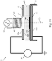
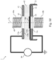
- Fig.1a to Fig.1d
- schematically illustrates cross sectional views of examples of embodiments of DBD plasma reactors according to the invention comprising one dielectric layer;
- Fig.2a to Fig.2c
- schematically illustrates cross sectional views of examples of embodiments of DBD plasma reactors according to the invention comprising two dielectric layers;
- Fig.3a and Fig.3b
- schematically illustrate the induction of Eddy currents in a metal plate for two different magnetic field orientations;
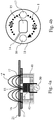
- Fig.4a
- is a cross sectional view of an induction heating coil, an electrode and a dielectric layer of a DBD plasma reactor according to the invention;
- Fig.4b
- is a top view of the electrode shown in
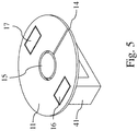
Fig.4a ; - Fig.5
- is a perspective view of an example of an electrode having a slit and a through-hole;
- Fig.6
- is a cross sectional view of an example of a pancake-type coil shown in combination with an electrode and a dielectric layer;
- Fig.7
- is a cross section view of an example of a pancake-type coil comprising a magnetic core;
- Fig.8.
- is a perspective view of an example of pancake type coil having a magnetic core;
- The figures are not drawn to scale. Generally, identical components are denoted by the same reference numerals in the figures.
- The present disclosure will be described in terms of specific embodiments, which are illustrative of the disclosure and not to be construed as limiting. It will be appreciated by persons skilled in the art that the present disclosure is not limited by what has been particularly shown and/or described and that alternatives or modified embodiments could be developed in the light of the overall teaching of this disclosure. The drawings described are only schematic and are non-limiting.
- Use of the verb "to comprise", as well as the respective conjugations, does not exclude the presence of elements other than those stated.
- Use of the article "a", "an" or "the" preceding an element does not exclude the presence of a plurality of such elements.
- Furthermore, the terms first, second and the like in the description and in the claims, are used for distinguishing between similar elements and not necessarily for describing a sequence, either temporally, spatially, in ranking or in any other manner. It is to be understood that the terms so used are interchangeable under appropriate circumstances and that the embodiments of the disclosure described herein are capable of operation in other sequences than described or illustrated herein.
- In
Fig.1a to Fig.1d andFig.2a to Fig.2c , examples of embodiments of dielectric barrier discharge (DBD)plasma reactors 1 for plasma enhanced chemical vapor deposition of a coating on a substrate under atmospheric pressure according to the present invention are shown. - Such a
DBD plasma reactor 1 comprises afirst electrode 11 separated from asecond electrode 12. Thefirst electrode 11 has afirst face 11a and asecond face 11b opposite to thefirst face 11a, and thesecond electrode 12 has a third 12a and afourth face 12b, opposite to the third face. As schematically shown onFig.1a to Fig.1c ,Fig.2a andFig.2b , thefourth face 12b of the second electrode is facing thesecond face 11b of the first electrode. By separating the first and second electrode, aplasma area 62 between thesecond face 11b and thefourth face 12b is formed, as illustrated with a dotted area on the figures mentioned above. - The first electrode is for example a ground electrode and the second electrode is a high-voltage electrode and a voltage can be applied between the first and second electrode with a
power supply 30. In some embodiments, the voltage applied between the first and the second electrode is a direct pulsed voltage. Preferably, the electrodes are made of a good conducting material, such as for example copper or aluminum. - The fact that the
second face 11b and thefourth face 12b are facing each other does not imply that no other elements are placed between the two faces. As further explained below, depending on the specific embodiment, between thesecond face 11b and thefourth face 12b one or more dielectric layers or additionally a susceptor can for example be placed. - The
DBD plasma reactor 1 shown onFig.1a andFig.1b comprises afirst dielectric layer 21 covering at least partly thesecond face 11b of the first electrode. - The DBD plasma reactor according to the invention is characterized in that it comprises an
induction heating coil 40 for heating by induction a substrate when placed in theplasma area 62 and/or for heating a susceptor by induction when placed in theplasma area 62. InFig.1a to Fig.1c ,Fig.2a andFig.2b ,reference 100 schematically illustrates a susceptor that is located on top of thefirst dielectric layer 21. In other embodiments, the substrate is directly positioned on thefirst dielectric layer 21 without use of a susceptor. - The induction heating coil is located outside of the plasma area. In the embodiment shown on
Fig.1a andFig.2a , thefirst face 11a of the first electrode is facing the inductingheating coil 40. In other words, in these examples, theinduction heating coil 40 is placed under the first electrode. In other embodiments, as for example shown onFig.1b ,Fig.1c andFig.2b , the induction heating coil is placed on top of the second electrode. In these examples, thethird face 12a of the second electrode is facing theinduction heating coil 40. - The
induction heating coil 40 is a coil comprising a plurality of windings winded around a central coil axis XB. Various embodiments of an induction heating coil will be further discussed below. The induction heating coil is powered by apower supply 50 for providing an alternating current in the coil, typically at a frequency in the kHz range, for example a frequency in range between 1 kHz and 100 kHz. - The DBD reactor according to the present invention is not limited to embodiments having only one induction heating coil. Indeed, in some embodiments the DBD reactor comprises more than one induction heating coil. For example, as schematically illustrated on
Fig.1d andFig.2c , twoinduction heating coils - The DBD plasma reactor according the invention is further characterized in that the
first electrode 11 and/or thesecond electrode 12 comprises a through-hole 15 extending along the central coil axis XB. InFig.1a andFig.2a , examples are shown of embodiments wherein the first electrode comprises a through-hole whileFig.1b shows an example wherein the through-hole is made in the second electrode. InFig.1c andFig.2b , examples of embodiments are shown wherein both the first 11 and the second 12 electrode comprise a through-hole 15. The role of the through-hole 15 will be further discussed. - The DBD plasma reactor of the current invention is not limited to one dielectric layer. For example in
Fig.2a andFig.2b , embodiments of a reactor are shown comprising asecond dielectric layer 22 covering at least partly thefourth face 12b of thesecond electrode 12. - The DBD plasma reactor is suitable to operate under atmospheric pressure, which is to be construed as operating in pressure ranges between 100 torr and 1000 torr. Typically, a DBD plasma reactor comprises a gas injection system configured to introduce gases into the plasma area. For example a main gas, such as e.g. argon, or helium or any other noble gas, can be introduced in the plasma area. The word "main gas" is used in order to distinguish the noble gas from other additional gases that could be introduced in the plasma area. Indeed, in some embodiments, besides the main gas, also a precursor under gaseous form is introduced into the plasma area. In some embodiments, as schematically illustrated on
Fig.2a , achamber 60 is used that is containing at least the first electrode, the second electrode and the induction heating coil. For DBD plasma reactors comprising a chamber, agas inlet 61 is generally provided to supply gas to the chamber. The arrow onFig.2a schematically indicates a gas flow direction when entering the chamber. - In other embodiments, no chamber is required when for example the DBD plasma reactor is located in an atmospheric pressure controlled environment and wherein a gas can directly be introduced in the plasma area.
- The
power supply 30 for the electrodes is commercially available and is for example supplying an alternating voltage, e.g. generating an alternating voltage in the kHz range, for example a frequency between 1 and 30 kHz. In other embodiments, the power supply provides a pulsed DC voltage. - In the embodiment illustrated on
Fig.1a , a central portion of thefirst electrode 11 and a central portion of thesecond electrode 12 are planar and parallel. In other embodiments, the electrodes do not necessarily have portions that are planar and/or parallel. In further embodiments, the second face of the first electrode and the fourth face of the second electrode are planar and/or parallel. - Preferably, the first and/or second electrode is/are made of non-magnetic metals.
- The goal of using an induction heating coil as mentioned above is to heat the substrate and/or susceptor and not to heat the electrode. Indeed, it is well known that Eddy currents induced in a metal by a varying magnetic field can heat the metal. This is schematically illustrated on
Fig.3a and Fig.3b , where two exemplary orientations of a magnetic field generated by an induction coil with respect to ametal plate 90 are shown. InFig.3a , the magnetic field lines are crossing themetal plate 90 transversally, resulting in Eddy currents, indicated by the reference "I" on the figure, flowing in circles in the plane of themetal plate 90. On the other hand, for the configuration shown inFig.3b , the magnetic field lines pass through the metal plate longitudinally, in a plane parallel with the metal plate. With the latter configuration, the induced Eddy currents will flow through the thickness of the metal plate in small loops as schematically illustrated onFig.3b . The skin depth δ, being the thickness used by the current to flow, also plays a role when designing the first electrode and/or the susceptor as will be further explained below. The equation defining the skin depth is well known in the art and the skin depth δ depends on the frequency of the varying magnetic field inducing the Eddy currents and on the electrical conductivity and magnetic permeability of the material wherein the Eddy currents are induced. - In some embodiments, the DBD plasma reactor comprises a susceptor. Indeed, to achieve a good heating of any kind of substrate, either metallic or non-metallic, it is preferred to add a metallic component placed under the substrate that will be uniformly heated by induction. This metallic component is called the "susceptor". This susceptor can be made of any kind of metal, but a ferromagnetic metal like nickel or iron will be far more susceptible to induction heating than a non-ferromagnetic metal like copper or aluminum, due to the contribution of the magnetic permeability to the skin depth and the hysteresis losses. The electric resistance of the conductor is also important as a high resistance metal will heat faster than a low resistance metal due to Joule effect. In induction heating, the skin effect is also an important factor for heating. The susceptor will be a thin sheet or grid of ferromagnetic metal preferably with high resistance. It should withstand a high temperature without oxidation, melting or chemical modification. Suitable materials are Iron, Nickel, Cobalt and any other ferromagnetic alloy with a high Curie temperature and with a reasonable resistance.
- If the substrate is a conducting material, it is not absolutely necessary to use an additional susceptor and the substrate can for example directly be placed on top of the first dielectric layer for being heated by induction by the induction heating coil.
- The
induction heating coil 40 that is schematically shown onFig.1a to Fig.1c ,Fig.2a andFig.2b is a coil wherein the plurality of windings are forming a so-called helix-type coil extending along the central coil axis XB. This type of coil can also be named solenoid shaped coil. The windings are typically made with Litz wire. - When such a helix-type coil is placed for example under the first electrode such that the central coil axis is perpendicular to the first electrode, as shown on
Fig.1a andFig.2a , the magnetic field lines are similar to the magnetic field lines shown onFig.3a , i.e. the magnetic field lines are crossing the first electrode in a direction parallel with the central coil axis. If the first electrode would not have the through-hole 15, the first electrode would be heated by the induced Eddy currents circulating in the first electrode. By providing the through-hole 15 in the first electrode, the magnetic field lines are passing through the through-hole 15, thereby avoiding or reducing induction heating in the first electrode. The person skilled in the art will design the dimension of the opening of the through-hole 15 in accordance with the dimension of the induction heating coil. If the through-hole has a circular opening, the diameter can for example be chosen to be equal or slightly larger than an external dimeter of a solenoid shaped coil used as induction coil, as schematically shown onFig.1a andFig.2a . - The same reasoning can be made for a DBD reactor configuration wherein the induction heating coil is placed on top of the second electrode and wherein the second electrode comprise a through-hole, as shown on
Fig.1b . In alternative embodiments, as shown onFig.1c andFig.2b , to reduce the heating of both electrodes, a through-hole 15 is provided in each of the two electrodes. - Remark that the exact location of the induction heating coil outside the plasma area is not important for the current invention, as long as the through-hole is extending along the central coil axis of the induction heating coil.
- Remark also that the
dielectric layer 21 partially covering the first electrode is not affecting the magnetic field lines as a dielectric is not a magnetic material. In embodiments, in addition to the provision of the through-hole 15, the induction current in the first electrode can be further reduced or eliminated by providing aslit 14 in the electrode. In preferred embodiments, theslit 14 is extending from an inner perimeter delimiting the through-hole 15 of the first electrode to an outer perimeter of thefirst electrode 11. The slit brakes the closed electrical circuit when formed in the first electrode such that no circular Eddy currents can circulate. Aslit 14 is schematically shown onFig.4b for an embodiment wherein the through-hole 15 has a rounded square shape. The two crosses onFig.4b schematically illustrate that due to theslit 14 no Eddy currents I can circulate as the closed circuit is broken by theslit 14. - In embodiments, as illustrated on
Fig.4a , in order to better concentrate the magnetic field in the center of theinduction coil 40, i.e. concentrate the magnetic field linesB along the central coil axis, theinduction heating coil 40 comprises amagnetic core 41, for example a ferrite core. In this particular embodiment, shown onFig.4a , in addition to the through-hole 15,additional holes first electrode 11. The location of these additional holes match with corresponding components of themagnetic core 41. Theadditional holes Fig.4b which is a top view of the electrode shown onFig.4a . This is further illustrated onFig.5 where a perspective view is shown of thefirst electrode 11 and part of theferrite core 41 shown onFig.4a . - In other embodiments, the DBD plasma reactor is using a pancake-type of induction coil as schematically shown on
Fig.6 . InFig.6 , thefirst electrode 11, thefirst dielectric layer 21 and theinduction coil 40 of the pancake-type are shown. A pancake-type of coil, also named flat coil, is a coil wherein the plurality of windings of the coil around a central coil axis XB are located in a plane. This type of pancake coil allows to generate longitudinal field lines, similar to field lines shown onFig.3b , in a susceptor arranged on thefirst dielectric layer 21. However, the magnetic field lines of a pancake-type coil are not completely longitudinal and in the center along the central coil axis XB, the magnetic field lines are aligned in the direction of the central coil axis XB and hence these transverse magnetic field lines have to cross through the first electrode before reaching the susceptor. Therefore, for the same reasons as discussed above for the helix-type coil, also for the pancake-type coil, a through-hole 15 extending along the central common coil axis XB is provided in thefirst electrode 11 in order to avoid or reduce Eddy currents in the plane of the first electrode induced by a varying transverse magnetic field. - When a pancake-type coil is used as an induction coil, the heating of the first electrode by Eddy currents resulting from the varying longitudinal magnetic field, as illustrated on
Fig.3b , can be strongly reduced or avoided by selecting the thickness S of the first electrode in relation to the skin depth. Indeed, it is known, that if the ratio S/δ between the thickness S of the conductor and the skin depth δ is below 2, the power efficiency of the induction heating drops drastically. This is described in for example the publication "Induction heating of thin slabs and sheets in the rolling line", D. Wohlfahrt and R. Jurgens, in 51st Internationales Wissenschaftliches Kolloquium Technische Universität Ilmenau September 11 - 15, 2006. In other words, if the metal thickness of the first electrode is selected such that the ratio S/δ is well below 2, the induction heating power is nearly zero and the first electrode will not be heated up. - In embodiments, the ratio between the thickness S of the first electrode and the skin depth δ of the first electrode is smaller than 1, preferably smaller than 0.5, more preferably equal or smaller than 0.1.
- The material selected for the first electrode is important as the material needs to have on the one hand a good conductivity and on the other hand have a low magnetic permeability. Indeed the electrode needs at the same time to be a good conductor for the high voltage and also have a low ratio S/δ, preferably have a skin depth of for example five times or ten time larger than the thickness S of the electrode. Usual non-magnetic metals like copper, aluminum and silver have approximatively the same skin depth and need to be 1 µm thick or thinner to avoid any induction heating with 100 kHz current frequency. Carbon graphite is a good alternative as it has an anisotropic conductivity that reduces the skin depth to some millimeters but keeping a good conductivity.
- In embodiments, as illustrated on
Fig.7 , the pancake-type of induction coil, also comprises amagnetic core 41, e.g. made of ferrite or another magnetic material, configured such that the magnetic field lines are bent and concentrated in the region where the induction heating is needed, i.e. at the location where the susceptor and/or the substrate are positioned. Magnetic fields linesB resulting from the pancake-induction coil are schematically shown as dotted lines onFig.7 . - According to a further aspect of the invention, a method for plasma-enhanced chemical vapor deposition of a coating on a substrate under atmospheric pressure using a dielectric barrier discharge plasma reactor as discussed above is provided. Preferably the coating is a crystalline inorganic coating. Generally, two methods can be distinguished, depending on if the substrate is conductive or not.
- As discussed above, if the substrate is conductive, it is not always necessarily to use a susceptor. In that case, when the DBD plasma reactor does not comprise a susceptor the method for plasma-enhanced chemical vapor deposition of a coating on a substrate comprises steps of:
- placing a conductive substrate in the
plasma area 62, preferably arranging the substrate on the first dielectric layer, - powering the
induction heating coil 40 such that a varying magnetic field is generated in the substrate and the substrate is heated by induction, - introducing a main gas into the plasma area, preferably additionally introducing a precursor under gaseous form in the plasma area,
- using the
power supply 30 for applying a voltage, preferably an alternating voltage, between the first electrode and the second electrode so as to generate a plasma in the plasma area. - On the other hand, when the DBD plasma reactor comprises a susceptor as discussed above, the method for plasma-enhanced chemical vapor deposition of a coating on a substrate comprises steps of:
- placing a substrate on the
susceptor 100 such that a thermal contact is made between the susceptor and the substrate, - powering the
induction heating coil 40 such that a varying magnetic field is generated in thesusceptor 100 and thesusceptor 100 is heated by induction, - introducing a main gas into the plasma area, preferably additionally introducing a precursor under gaseous form into the plasma area,
- using the
power supply 30 for applying a voltage, preferably an alternating voltage, between the first electrode and the second electrode so as to generate a plasma in the plasma area. - The method according to the invention as described above and expressed in the appended claims, is not limited by the order of the steps given, in embodiments steps can be performed in a different order or some steps can be performed in parallel.
Claims (15)
- A dielectric barrier discharge plasma reactor (1) for plasma enhanced chemical vapor deposition of a coating on a substrate under atmospheric pressure, comprising:• a first electrode (11) having a first face (11a) and a second face (11b) opposite to the first face (11a),• a second electrode (12) having a third face (12a) and a fourth face (12b) opposite to the third face, the fourth face (12b) of the second electrode facing the second face (11b) of the first electrode, and wherein the second electrode is separated from the first electrode (11) for forming a plasma area (62) between the second face (11b) and the fourth face (12b),• a first dielectric layer (21) covering at least partly the second face (11b) of the first electrode,• a power supply (30) configured to apply a voltage between the first and second electrode,characterized in that
the reactor (1) further comprises an induction heating coil (40) for heating by induction the substrate when placed in the plasma area (62) and/or for heating a susceptor by induction when placed in the plasma area (62), said induction heating coil being located outside of said plasma area, and wherein said induction heating coil (40) comprises a plurality of windings (45) winded around a central coil axis (XB),
and in that said first electrode (11) and/or said second electrode (12) comprises a through-hole (15) extending along said central coil axis (XB). - A dielectric barrier discharge plasma reactor according to claim 1, further comprising a second dielectric layer (22) covering at least partly said fourth face (12b) of the second electrode.
- A dielectric barrier discharge plasma reactor according to any of the previous claims, wherein at least a central portion of said second face (11b) and a central portion of said fourth face (12b) are planar and parallel.
- A dielectric barrier discharge plasma reactor according to any of previous claims, wherein said plurality of windings (45) of the induction heating coil (40) are forming a helix-type coil extending along said central coil axis (XB).
- A dielectric barrier discharge plasma reactor according to any of claims 1 to 3, wherein said plurality of windings (45) of the induction heating coil (40) are located in a plane so as to form a pancake-type coil.
- A dielectric barrier discharge plasma reactor according to claim 5, wherein a ratio between a thickness (S) of the first electrode and a skin depth (δ) of the first electrode and/or a ratio between a thickness (S) of the second electrode and a skin depth (δ) of the second electrode is smaller than 1, preferably smaller than 0.5, more preferably equal or smaller than 0.1.
- A dielectric barrier discharge plasma reactor according to any of the previous claims, wherein said induction heating coil (40) comprises a magnetic core (41), preferably a ferrite core.
- A dielectric barrier discharge plasma reactor according to any of the previous claims, wherein the first electrode (11) and/or second electrode (12) further comprises a slit (14) for suppressing Eddy currents, preferably said slit is extending from an inner perimeter delimiting the through-hole (15) of the electrode to an outer perimeter of the electrode.
- A dielectric barrier discharge plasma reactor according to any of the previous claims, wherein said coating is a crystalline inorganic coating, preferably comprising a transition metal oxide.
- A dielectric barrier discharge plasma reactor according to any of the previous claims, wherein the first and/or second electrode is/are made of non-magnetic metals.
- A dielectric barrier discharge plasma reactor according to any of the previous claims, further comprising a gas injection system configured to introduce a gas into the plasma area.
- A dielectric barrier discharge plasma reactor according to any of the previous claims, further comprising a chamber containing at least the first electrode, the second electrode and the first dielectric layer, preferably the chamber has a gas inlet (61).
- A dielectric barrier discharge plasma reactor according to any of previous claims, further comprising a susceptor (100) arranged on said first dielectric layer (21).
- A method for plasma-enhanced chemical vapor deposition of a coating on a substrate under atmospheric pressure using a dielectric barrier discharge plasma reactor according to any of claims 1 to 13, said method comprising the steps of:• placing the substrate on the first dielectric layer or placing a susceptor on the first dielectric layer and placing the substrate on the susceptor (100) such that a thermal contact is made between the susceptor and the substrate;• powering the induction heating coil (40) such that a varying magnetic field is generated in said substrate and/or said susceptor,• introducing a main gas into the plasma area, preferably additionally introducing a precursor under gaseous form in the plasma area,• using the power supply (30) for applying a voltage, preferably an alternating voltage, between the first electrode and the second electrode so as to generate a plasma in the plasma area.
- A method according to claim 14, wherein said coating is a crystalline inorganic coating, preferably comprising a transition metal oxide.
Priority Applications (1)
| Application Number | Priority Date | Filing Date | Title |
|---|---|---|---|
| EP19187406.4A EP3768048B1 (en) | 2019-07-19 | 2019-07-19 | Dielectric barrier discharge plasma reactor and method for plasma-enhanced vapor deposition |
Applications Claiming Priority (1)
| Application Number | Priority Date | Filing Date | Title |
|---|---|---|---|
| EP19187406.4A EP3768048B1 (en) | 2019-07-19 | 2019-07-19 | Dielectric barrier discharge plasma reactor and method for plasma-enhanced vapor deposition |
Publications (3)
| Publication Number | Publication Date |
|---|---|
| EP3768048A1 true EP3768048A1 (en) | 2021-01-20 |
| EP3768048C0 EP3768048C0 (en) | 2023-06-07 |
| EP3768048B1 EP3768048B1 (en) | 2023-06-07 |
Family
ID=67438241
Family Applications (1)
| Application Number | Title | Priority Date | Filing Date |
|---|---|---|---|
| EP19187406.4A Active EP3768048B1 (en) | 2019-07-19 | 2019-07-19 | Dielectric barrier discharge plasma reactor and method for plasma-enhanced vapor deposition |
Country Status (1)
| Country | Link |
|---|---|
| EP (1) | EP3768048B1 (en) |
Citations (4)
| Publication number | Priority date | Publication date | Assignee | Title |
|---|---|---|---|---|
| US5510158A (en) * | 1993-11-26 | 1996-04-23 | Ushiodenki Kabushiki Kaisha | Process for oxidation of an article |
| US20050236374A1 (en) * | 2004-04-01 | 2005-10-27 | Lincoln Global, Inc. | Device for processing welding wire |
| JP2006032303A (en) * | 2004-07-22 | 2006-02-02 | Sharp Corp | High frequency plasma processing apparatus and processing method |
| KR101507383B1 (en) * | 2013-10-01 | 2015-03-31 | 한국표준과학연구원 | Inductive Heating Graphene Forming Apparatus and Graphene Forming Method |
-
2019
- 2019-07-19 EP EP19187406.4A patent/EP3768048B1/en active Active
Patent Citations (4)
| Publication number | Priority date | Publication date | Assignee | Title |
|---|---|---|---|---|
| US5510158A (en) * | 1993-11-26 | 1996-04-23 | Ushiodenki Kabushiki Kaisha | Process for oxidation of an article |
| US20050236374A1 (en) * | 2004-04-01 | 2005-10-27 | Lincoln Global, Inc. | Device for processing welding wire |
| JP2006032303A (en) * | 2004-07-22 | 2006-02-02 | Sharp Corp | High frequency plasma processing apparatus and processing method |
| KR101507383B1 (en) * | 2013-10-01 | 2015-03-31 | 한국표준과학연구원 | Inductive Heating Graphene Forming Apparatus and Graphene Forming Method |
Non-Patent Citations (1)
| Title |
|---|
| D. WOHLFAHRTR. JURGENS: "Induction heating of thin slabs and sheets in the rolling line", 51ST INTERNATIONALES WISSENSCHAFTLICHES KOLLOQUIUM TECHNISCHE UNIVERSITAT ILMENAU, 11 September 2006 (2006-09-11) |
Also Published As
| Publication number | Publication date |
|---|---|
| EP3768048C0 (en) | 2023-06-07 |
| EP3768048B1 (en) | 2023-06-07 |
Similar Documents
| Publication | Publication Date | Title |
|---|---|---|
| US11450509B2 (en) | Inductive plasma source with metallic shower head using b-field concentrator | |
| US7255774B2 (en) | Process apparatus and method for improving plasma production of an inductively coupled plasma | |
| US9530619B2 (en) | Plasma processing apparatus and filter unit | |
| JP5257917B2 (en) | Inductively coupled plasma reactor with multiple magnetic cores | |
| US5998933A (en) | RF plasma inductor with closed ferrite core | |
| EP1089319B1 (en) | Uniform gas distribution in large area plasma treatment device | |
| EP1727186B1 (en) | Plasma chamber with discharge inducing bridge | |
| EP2020160B1 (en) | Electric induction heat treatment of an end of tubular material | |
| US7163602B2 (en) | Apparatus for generating planar plasma using concentric coils and ferromagnetic cores | |
| JP3190690B2 (en) | Method and apparatus for generating large-scale induction plasma for plasma processing | |
| US5541566A (en) | Diamond-like carbon coating for magnetic cores | |
| JP4579534B2 (en) | Method and apparatus for controlling the temperature of an object | |
| TW201143552A (en) | Plasma source design | |
| CN107004561A (en) | Plasma process system with directly exported toroidal plasma source | |
| TW201143547A (en) | Plasma processing apparatus | |
| KR102125028B1 (en) | Cooling kit and a plasma reactor having the same magnetic core for cooling | |
| JP2024012449A (en) | stage | |
| US6475333B1 (en) | Discharge plasma processing device | |
| JP2004200169A (en) | Electromagnetic induction accelerator | |
| JP7422077B2 (en) | High power radio frequency helical coil filter | |
| EP3768048B1 (en) | Dielectric barrier discharge plasma reactor and method for plasma-enhanced vapor deposition | |
| KR20230119210A (en) | Ion source in which the coil structure can be changed according to the discharge chamber structure | |
| KR100805557B1 (en) | Inductively Coupled Plasma Sources with Multiple Magnetic Cores | |
| KR102001030B1 (en) | Radio frequency(rf) antenna, method of forming the same, and ion source | |
| JP2019527486A (en) | Variable magnetic monopole field electromagnet and inductor |
Legal Events
| Date | Code | Title | Description |
|---|---|---|---|
| PUAI | Public reference made under article 153(3) epc to a published international application that has entered the european phase |
Free format text: ORIGINAL CODE: 0009012 |
|
| STAA | Information on the status of an ep patent application or granted ep patent |
Free format text: STATUS: THE APPLICATION HAS BEEN PUBLISHED |
|
| AK | Designated contracting states |
Kind code of ref document: A1 Designated state(s): AL AT BE BG CH CY CZ DE DK EE ES FI FR GB GR HR HU IE IS IT LI LT LU LV MC MK MT NL NO PL PT RO RS SE SI SK SM TR |
|
| AX | Request for extension of the european patent |
Extension state: BA ME |
|
| STAA | Information on the status of an ep patent application or granted ep patent |
Free format text: STATUS: REQUEST FOR EXAMINATION WAS MADE |
|
| 17P | Request for examination filed |
Effective date: 20210712 |
|
| RBV | Designated contracting states (corrected) |
Designated state(s): AL AT BE BG CH CY CZ DE DK EE ES FI FR GB GR HR HU IE IS IT LI LT LU LV MC MK MT NL NO PL PT RO RS SE SI SK SM TR |
|
| GRAP | Despatch of communication of intention to grant a patent |
Free format text: ORIGINAL CODE: EPIDOSNIGR1 |
|
| STAA | Information on the status of an ep patent application or granted ep patent |
Free format text: STATUS: GRANT OF PATENT IS INTENDED |
|
| INTG | Intention to grant announced |
Effective date: 20220720 |
|
| GRAJ | Information related to disapproval of communication of intention to grant by the applicant or resumption of examination proceedings by the epo deleted |
Free format text: ORIGINAL CODE: EPIDOSDIGR1 |
|
| STAA | Information on the status of an ep patent application or granted ep patent |
Free format text: STATUS: REQUEST FOR EXAMINATION WAS MADE |
|
| INTC | Intention to grant announced (deleted) | ||
| GRAP | Despatch of communication of intention to grant a patent |
Free format text: ORIGINAL CODE: EPIDOSNIGR1 |
|
| STAA | Information on the status of an ep patent application or granted ep patent |
Free format text: STATUS: GRANT OF PATENT IS INTENDED |
|
| INTG | Intention to grant announced |
Effective date: 20230103 |
|
| GRAS | Grant fee paid |
Free format text: ORIGINAL CODE: EPIDOSNIGR3 |
|
| GRAA | (expected) grant |
Free format text: ORIGINAL CODE: 0009210 |
|
| STAA | Information on the status of an ep patent application or granted ep patent |
Free format text: STATUS: THE PATENT HAS BEEN GRANTED |
|
| AK | Designated contracting states |
Kind code of ref document: B1 Designated state(s): AL AT BE BG CH CY CZ DE DK EE ES FI FR GB GR HR HU IE IS IT LI LT LU LV MC MK MT NL NO PL PT RO RS SE SI SK SM TR |
|
| REG | Reference to a national code |
Ref country code: GB Ref legal event code: FG4D |
|
| REG | Reference to a national code |
Ref country code: CH Ref legal event code: EP Ref country code: AT Ref legal event code: REF Ref document number: 1578461 Country of ref document: AT Kind code of ref document: T Effective date: 20230615 Ref country code: DE Ref legal event code: R096 Ref document number: 602019029821 Country of ref document: DE |
|
| U01 | Request for unitary effect filed |
Effective date: 20230607 |
|
| U07 | Unitary effect registered |
Designated state(s): AT BE BG DE DK EE FI FR IT LT LU LV MT NL PT SE SI Effective date: 20230612 |
|
| U1B | Unitary effect: place of business changed | ||
| U1N | Appointed representative for the unitary patent procedure changed after the registration of the unitary effect |
Representative=s name: ICOSA EUROPE; BE |
|
| REG | Reference to a national code |
Ref country code: LT Ref legal event code: MG9D |
|
| U20 | Renewal fee for the european patent with unitary effect paid |
Year of fee payment: 5 Effective date: 20230824 |
|
| PG25 | Lapsed in a contracting state [announced via postgrant information from national office to epo] |
Ref country code: NO Free format text: LAPSE BECAUSE OF FAILURE TO SUBMIT A TRANSLATION OF THE DESCRIPTION OR TO PAY THE FEE WITHIN THE PRESCRIBED TIME-LIMIT Effective date: 20230907 Ref country code: ES Free format text: LAPSE BECAUSE OF FAILURE TO SUBMIT A TRANSLATION OF THE DESCRIPTION OR TO PAY THE FEE WITHIN THE PRESCRIBED TIME-LIMIT Effective date: 20230607 |
|
| PG25 | Lapsed in a contracting state [announced via postgrant information from national office to epo] |
Ref country code: RS Free format text: LAPSE BECAUSE OF FAILURE TO SUBMIT A TRANSLATION OF THE DESCRIPTION OR TO PAY THE FEE WITHIN THE PRESCRIBED TIME-LIMIT Effective date: 20230607 Ref country code: HR Free format text: LAPSE BECAUSE OF FAILURE TO SUBMIT A TRANSLATION OF THE DESCRIPTION OR TO PAY THE FEE WITHIN THE PRESCRIBED TIME-LIMIT Effective date: 20230607 Ref country code: GR Free format text: LAPSE BECAUSE OF FAILURE TO SUBMIT A TRANSLATION OF THE DESCRIPTION OR TO PAY THE FEE WITHIN THE PRESCRIBED TIME-LIMIT Effective date: 20230908 |
|
| PG25 | Lapsed in a contracting state [announced via postgrant information from national office to epo] |
Ref country code: SK Free format text: LAPSE BECAUSE OF FAILURE TO SUBMIT A TRANSLATION OF THE DESCRIPTION OR TO PAY THE FEE WITHIN THE PRESCRIBED TIME-LIMIT Effective date: 20230607 |
|
| PG25 | Lapsed in a contracting state [announced via postgrant information from national office to epo] |
Ref country code: IS Free format text: LAPSE BECAUSE OF FAILURE TO SUBMIT A TRANSLATION OF THE DESCRIPTION OR TO PAY THE FEE WITHIN THE PRESCRIBED TIME-LIMIT Effective date: 20231007 |
|
| PG25 | Lapsed in a contracting state [announced via postgrant information from national office to epo] |
Ref country code: SM Free format text: LAPSE BECAUSE OF FAILURE TO SUBMIT A TRANSLATION OF THE DESCRIPTION OR TO PAY THE FEE WITHIN THE PRESCRIBED TIME-LIMIT Effective date: 20230607 Ref country code: SK Free format text: LAPSE BECAUSE OF FAILURE TO SUBMIT A TRANSLATION OF THE DESCRIPTION OR TO PAY THE FEE WITHIN THE PRESCRIBED TIME-LIMIT Effective date: 20230607 Ref country code: RO Free format text: LAPSE BECAUSE OF FAILURE TO SUBMIT A TRANSLATION OF THE DESCRIPTION OR TO PAY THE FEE WITHIN THE PRESCRIBED TIME-LIMIT Effective date: 20230607 Ref country code: IS Free format text: LAPSE BECAUSE OF FAILURE TO SUBMIT A TRANSLATION OF THE DESCRIPTION OR TO PAY THE FEE WITHIN THE PRESCRIBED TIME-LIMIT Effective date: 20231007 Ref country code: CZ Free format text: LAPSE BECAUSE OF FAILURE TO SUBMIT A TRANSLATION OF THE DESCRIPTION OR TO PAY THE FEE WITHIN THE PRESCRIBED TIME-LIMIT Effective date: 20230607 |
|
| PG25 | Lapsed in a contracting state [announced via postgrant information from national office to epo] |
Ref country code: PL Free format text: LAPSE BECAUSE OF FAILURE TO SUBMIT A TRANSLATION OF THE DESCRIPTION OR TO PAY THE FEE WITHIN THE PRESCRIBED TIME-LIMIT Effective date: 20230607 |
|
| REG | Reference to a national code |
Ref country code: CH Ref legal event code: PL |
|
| REG | Reference to a national code |
Ref country code: DE Ref legal event code: R097 Ref document number: 602019029821 Country of ref document: DE |
|
| PG25 | Lapsed in a contracting state [announced via postgrant information from national office to epo] |
Ref country code: MC Free format text: LAPSE BECAUSE OF FAILURE TO SUBMIT A TRANSLATION OF THE DESCRIPTION OR TO PAY THE FEE WITHIN THE PRESCRIBED TIME-LIMIT Effective date: 20230607 |
|
| PG25 | Lapsed in a contracting state [announced via postgrant information from national office to epo] |
Ref country code: MC Free format text: LAPSE BECAUSE OF FAILURE TO SUBMIT A TRANSLATION OF THE DESCRIPTION OR TO PAY THE FEE WITHIN THE PRESCRIBED TIME-LIMIT Effective date: 20230607 |
|
| PLBE | No opposition filed within time limit |
Free format text: ORIGINAL CODE: 0009261 |
|
| STAA | Information on the status of an ep patent application or granted ep patent |
Free format text: STATUS: NO OPPOSITION FILED WITHIN TIME LIMIT |
|
| REG | Reference to a national code |
Ref country code: IE Ref legal event code: MM4A |
|
| PG25 | Lapsed in a contracting state [announced via postgrant information from national office to epo] |
Ref country code: CH Free format text: LAPSE BECAUSE OF NON-PAYMENT OF DUE FEES Effective date: 20230731 |
|
| 26N | No opposition filed |
Effective date: 20240308 |
|
| GBPC | Gb: european patent ceased through non-payment of renewal fee |
Effective date: 20230907 |
|
| PG25 | Lapsed in a contracting state [announced via postgrant information from national office to epo] |
Ref country code: IE Free format text: LAPSE BECAUSE OF NON-PAYMENT OF DUE FEES Effective date: 20230719 |
|
| PG25 | Lapsed in a contracting state [announced via postgrant information from national office to epo] |
Ref country code: GB Free format text: LAPSE BECAUSE OF NON-PAYMENT OF DUE FEES Effective date: 20230907 |
|
| PG25 | Lapsed in a contracting state [announced via postgrant information from national office to epo] |
Ref country code: IE Free format text: LAPSE BECAUSE OF NON-PAYMENT OF DUE FEES Effective date: 20230719 Ref country code: GB Free format text: LAPSE BECAUSE OF NON-PAYMENT OF DUE FEES Effective date: 20230907 |
|
| U20 | Renewal fee for the european patent with unitary effect paid |
Year of fee payment: 6 Effective date: 20240724 |
|
| PG25 | Lapsed in a contracting state [announced via postgrant information from national office to epo] |
Ref country code: CY Free format text: LAPSE BECAUSE OF FAILURE TO SUBMIT A TRANSLATION OF THE DESCRIPTION OR TO PAY THE FEE WITHIN THE PRESCRIBED TIME-LIMIT; INVALID AB INITIO Effective date: 20190719 |
|
| PG25 | Lapsed in a contracting state [announced via postgrant information from national office to epo] |
Ref country code: HU Free format text: LAPSE BECAUSE OF FAILURE TO SUBMIT A TRANSLATION OF THE DESCRIPTION OR TO PAY THE FEE WITHIN THE PRESCRIBED TIME-LIMIT; INVALID AB INITIO Effective date: 20190719 |
|
| U20 | Renewal fee for the european patent with unitary effect paid |
Year of fee payment: 7 Effective date: 20250728 |
|
| PG25 | Lapsed in a contracting state [announced via postgrant information from national office to epo] |
Ref country code: TR Free format text: LAPSE BECAUSE OF FAILURE TO SUBMIT A TRANSLATION OF THE DESCRIPTION OR TO PAY THE FEE WITHIN THE PRESCRIBED TIME-LIMIT Effective date: 20230607 |