EP3767749A1 - Split-ring resonator, baseplate, and connector - Google Patents
Split-ring resonator, baseplate, and connector Download PDFInfo
- Publication number
- EP3767749A1 EP3767749A1 EP19785015.9A EP19785015A EP3767749A1 EP 3767749 A1 EP3767749 A1 EP 3767749A1 EP 19785015 A EP19785015 A EP 19785015A EP 3767749 A1 EP3767749 A1 EP 3767749A1
- Authority
- EP
- European Patent Office
- Prior art keywords
- split
- ring resonator
- conductor
- present disclosure
- ground terminal
- Prior art date
- Legal status (The legal status is an assumption and is not a legal conclusion. Google has not performed a legal analysis and makes no representation as to the accuracy of the status listed.)
- Granted
Links
Images














Classifications
-
- H—ELECTRICITY
- H01—ELECTRIC ELEMENTS
- H01Q—ANTENNAS, i.e. RADIO AERIALS
- H01Q9/00—Electrically-short antennas having dimensions not more than twice the operating wavelength and consisting of conductive active radiating elements
- H01Q9/04—Resonant antennas
- H01Q9/0485—Dielectric resonator antennas
-
- H—ELECTRICITY
- H01—ELECTRIC ELEMENTS
- H01Q—ANTENNAS, i.e. RADIO AERIALS
- H01Q9/00—Electrically-short antennas having dimensions not more than twice the operating wavelength and consisting of conductive active radiating elements
- H01Q9/04—Resonant antennas
- H01Q9/0407—Substantially flat resonant element parallel to ground plane, e.g. patch antenna
-
- H—ELECTRICITY
- H01—ELECTRIC ELEMENTS
- H01P—WAVEGUIDES; RESONATORS, LINES, OR OTHER DEVICES OF THE WAVEGUIDE TYPE
- H01P1/00—Auxiliary devices
- H01P1/20—Frequency-selective devices, e.g. filters
- H01P1/201—Filters for transverse electromagnetic waves
- H01P1/203—Strip line filters
- H01P1/20309—Strip line filters with dielectric resonator
-
- H—ELECTRICITY
- H01—ELECTRIC ELEMENTS
- H01Q—ANTENNAS, i.e. RADIO AERIALS
- H01Q1/00—Details of, or arrangements associated with, antennas
- H01Q1/36—Structural form of radiating elements, e.g. cone, spiral, umbrella; Particular materials used therewith
-
- H—ELECTRICITY
- H01—ELECTRIC ELEMENTS
- H01Q—ANTENNAS, i.e. RADIO AERIALS
- H01Q1/00—Details of, or arrangements associated with, antennas
- H01Q1/36—Structural form of radiating elements, e.g. cone, spiral, umbrella; Particular materials used therewith
- H01Q1/38—Structural form of radiating elements, e.g. cone, spiral, umbrella; Particular materials used therewith formed by a conductive layer on an insulating support
-
- H—ELECTRICITY
- H01—ELECTRIC ELEMENTS
- H01Q—ANTENNAS, i.e. RADIO AERIALS
- H01Q1/00—Details of, or arrangements associated with, antennas
- H01Q1/48—Earthing means; Earth screens; Counterpoises
-
- H—ELECTRICITY
- H01—ELECTRIC ELEMENTS
- H01Q—ANTENNAS, i.e. RADIO AERIALS
- H01Q13/00—Waveguide horns or mouths; Slot antennas; Leaky-waveguide antennas; Equivalent structures causing radiation along the transmission path of a guided wave
- H01Q13/10—Resonant slot antennas
-
- H—ELECTRICITY
- H01—ELECTRIC ELEMENTS
- H01Q—ANTENNAS, i.e. RADIO AERIALS
- H01Q13/00—Waveguide horns or mouths; Slot antennas; Leaky-waveguide antennas; Equivalent structures causing radiation along the transmission path of a guided wave
- H01Q13/10—Resonant slot antennas
- H01Q13/16—Folded slot antennas
Definitions
- This invention relates to a split-ring resonator, a board and a connector.
- Patent Document 1 discloses a wireless communication device comprising a split-ring resonator.
- Patent Document 1 WO 2013/027824
- the split-ring resonator of Patent Document 1 is formed directly on a board while being connected to a ground pattern. Therefore, the split-ring resonator according to the aspect disclosed in Patent Document 1 neither can be distributed as a single component nor can be flexibly combined with the other component in accordance with design requirements. Thus, according to the aspect disclosed in Patent Document 1, the split-ring resonator cannot be used as a component.
- the object of an aspect of the present disclosure is to provide a split-ring resonator, a board and a connector for solving one or more of the problems described above.
- a split-ring resonator comprises a first ground terminal which is separated from a ground pattern.
- a board according to an aspect of the present disclosure comprises a terminal configured to be connected to a ground terminal, which is separated from a ground pattern, of a split-ring resonator according to an aspect of the present disclosure.
- a connector according to an aspect of the present disclosure comprises a terminal configured to be connected to a ground terminal, which is separated from a ground pattern, of a split-ring resonator according to an aspect of the present disclosure.
- Various aspects of the present disclosure enable a split-ring resonator to be used as a component.
- a split-ring resonator 11 according to an aspect of the present disclosure comprises a ground terminal 14 which is separated from a ground pattern.
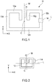
- Figs. 1, 2 and 3 are figures showing examples of the split-ring resonator 11 according to an aspect of the present disclosure.
- a center of a ring of the split-ring resonator 11 will be referred to as a point C.
- a line segment which connects a split of the split-ring resonator 11 and the point C to each other will be referred to as a line segment m.
- a straight-line which includes the line segment m will be referred to as a straight-line M.
- another straight-line which is perpendicular to the line segment m (or the straight-line M) and passes through the point C will be referred to as a straight-line L.
- the point C exists on the straight-line L.
- a direction in which the straight-line M extends will be referred to as the Y-axis direction.
- a direction in which the straight-line L extends will be referred to as the X-axis direction.
- the split-ring resonator 11 may comprise a split-ring 12.
- the split-ring 12 may be shaped into a C-like shape extending along a rectangular ring, the C-like shape being formed of: a split portion 12g; a first conductor 12a which extends in the X-axis direction while sandwiching the split portion 12g therebetween; a second conductor 12b which extends in the X-axis direction; a third conductor 12c which extends in the Y-axis direction; and a fourth conductor 12d which extends in the Y-axis direction.
- the split-ring 12 may have a shape which extends along one of various rings including a circular ring, an elliptical ring, a track-shaped ring and any other rings.
- the split-ring 12 may be formed of a metal plate.
- the split-ring resonator 11 may comprise the ground terminal 14 separated from a ground pattern.
- the split-ring resonator 11 may comprise not only the ground terminal 14 but also a plurality of the ground terminals 14 each separated from a ground pattern.
- the ground terminal 14 may have any structure, provided that the structure is electrically connectable with a ground pattern.
- the ground terminal 14 may be configured to be electrically connected with a ground pattern via soldering, pressure joining, a connector, a pin, etc.
- the ground terminal 14 may be a land pattern as shown in Fig. 1 .
- the ground terminal 14 may be a pattern which projects outward from the outer circumference of the split-ring resonator 11 as shown in Fig. 2 .
- the ground terminal 14 may be an exposed pattern which is formed by partially removing a coat of the split-ring resonator 11 as shown in Fig. 3 .
- the ground terminal 14 may have any structure, provided that the structure is electrically connectable with a ground pattern.
- the ground terminal 14 may be formed of a metal plate.
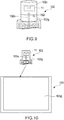
- Figs. 4 , 5 and 6 are figures showing examples of the split-ring resonator 11 according to an aspect of the present disclosure.
- Figs. 4 , 5 and 6 show a structure in which the split-ring resonator 11 comprises the one ground terminal 14.
- the split-ring resonator 11 may comprise two or more of the ground terminals.
- the split-ring resonator 11 may comprise the split-ring 12, the ground terminal 14 and a feeding terminal 13.
- the feeding terminal 13 may be formed of a wire and a metal plate.
- the feeding terminal 13 may be a terminal for supplying radio frequency (RF) signals to the split-ring 12.
- the feeding terminal 13 may be connected to the split-ring 12.
- the feeding terminal 13 may be connected to a transmission line.
- the feeding terminal 13 may be connected to the first conductor 12a.
- the split-ring resonator 11 may comprise the split-ring 12, the ground terminal 14, the feeding terminal 13 and a chip body 15.
- the split-ring resonator 11 may comprise the split-ring 12, the ground terminal 14, the feeding terminal 13 and a printed circuit board 15'.
- the split-ring 12, the ground terminal 14 and the feeding terminal 13 are provided on one of surfaces of the printed circuit board 15'.
- the printed circuit board 15' may have either a single-layer structure or a multi-layer structure.
- the split-ring 12, the ground terminal 14 and the feeding terminal 13 may be provided on one of layers thereof.
- a board according to an aspect of the present disclosure comprises a terminal configured to be connected to a ground terminal, which is separated from a ground pattern, of a split-ring resonator according to an aspect of the present disclosure.
- Figs. 7 and 8 are figures showing examples of a board 101 according to an aspect of the present disclosure.
- the board 101 may comprise a ground pattern 101g having a rectangular outline.
- the board 101 may comprise a reception terminal 101r.
- the reception terminal 101r may be a terminal configured to be connected to a ground terminal, which is separated from a ground pattern, of a split-ring resonator according to an aspect of the present disclosure.
- the board 101 may comprise an opening 101a which corresponds to a shape and a size of a split-ring resonator according to an aspect of the present disclosure. In this case, for example, as shown in Fig.
- an antenna may be formed by accommodating a split-ring resonator according to an aspect of the present disclosure in the opening 101a and by connecting the reception terminal 101r to a ground terminal, which is separated from a ground pattern, of the split-ring resonator according to an aspect of the present disclosure.
- the board 101 may comprise no opening which corresponds to a shape and a size of a split-ring resonator according to an aspect of the present disclosure. In this case, for example, as shown in Fig.
- an antenna may be formed by arranging a split-ring resonator according to an aspect of the present disclosure to be adjacent to a side or an edge of a ground pattern 101g' and by connecting the reception terminal 101r to a ground terminal, which is separated from a ground pattern, of the split-ring resonator according to an aspect of the present disclosure.
- a connector according to an aspect of the present disclosure comprises a terminal configured to be connected to a ground terminal, which is separated from a ground pattern, of a split-ring resonator according to an aspect of the present disclosure.
- Figs. 9 and 10 are figures showing examples of a connector 102 according to an aspect of the present disclosure.
- the connector 102 may comprise a ground pattern 102g.
- the connector 102 may comprise a reception terminal 102r.
- the connector 102 may comprise a feeding pattern 102s.
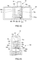
- the connector 102 may be shaped in a cylindrical shape whose axial direction is an extending direction of the feeding pattern 102s, and whose circumference surface is formed of the ground pattern 102g, so that the connector 102 may be formed as a coaxial connector having a central wire of the connector formed of the feeding pattern 102s and having an outer conductor of the connector formed of the ground pattern 102g.
- the ground pattern 102g may have a screw shape which is located at one of opposite ends of the connector 102 in the axial direction and may be electrically and mechanically connectable with another ground pattern having a corresponding screw shape.
- the connector 102 may comprise a dielectric cap 102c which is located at a remaining one of the opposite ends in the axial direction and is adjacent to the ground pattern 102g, so that the split-ring resonator 11 may be accommodatable in the dielectric cap 102c.
- the split-ring resonator 11 may be provided at the remaining one of the opposite ends of the connector 102 in the axial direction to be adjacent to the ground pattern 102g.
- the ground pattern 102g may be connected to the ground terminal 14 via the reception terminal 102r, and the feeding pattern 102s may be connected to the feeding terminal 13.
- the connector 102 may be a female connector with the ground pattern 102g having a female screw shape.
- the connector 102 may be connected to a main circuit board 103 having a male connector.
- the split-ring resonator 11 (ground terminal 14) may be connected to a main ground pattern 103g of the main circuit board 103 via the ground pattern 102g.
- the ground pattern 102g may have either a female screw shape or a male screw shape.
- the ground pattern 102g of the connector 102 may have a male screw shape, and the connector 102 may be connected to a main circuit board having a female connector.
- a current in accordance with RF signals can flow between the feeding terminal 13 and the ground terminal 14 of a split-ring resonator 21. Therefore, an antenna can be formed by combining the aforementioned split-ring resonator according to an aspect of the present disclosure to the aforementioned board according to an aspect of the present disclosure or the aforementioned connector according to an aspect of the present disclosure. Therefore, according to an aspect of the present disclosure described above, a split-ring resonator can be distributed as a single component and can be flexibly combined with the other component in accordance with design requirements.
- the split-ring resonator 21 is based on the split-ring resonator 11 while a first ground terminal is located on a section where a split of the split-ring resonator exists as viewed from the straight-line L.
- the point C exists, the point C being a center of a ring of the split-ring resonator.
- the straight-line L is perpendicular to the line segment m which connects the point C and the split to each other.
- Figs. 11, 12 , 13 and 14 are figures showing examples of the split-ring resonator 21 according to an aspect of the present disclosure.
- each section of a split-ring resonator will be defined as follows.
- a section where a split of a split-ring resonator is as viewed from the straight-line L is defined as an upper section RU of the split-ring resonator.
- an upper half part of the split-ring 12 i.e. a part formed of: the split portion 12g; the first conductor 12a; a part of the third conductor 12c which is nearer to the first conductor 12a than to the second conductor 12b; and a part of the fourth conductor 12d which is nearer to the first conductor 12a than to the second conductor 12b
- the split-ring 12 may be configured to be the upper section RU of the split-ring resonator.
- a section opposite to the section for the split of the split-ring resonator across the straight-line L is defined as a lower section RD of the split-ring resonator.
- a lower half part of the split-ring 12 i.e. a part formed of: the second conductor 12b; a part of the third conductor 12c which is nearer to the second conductor 12b than to the first conductor 12a; and a part of the fourth conductor 12d which is nearer to the second conductor 12b than to the first conductor 12a
- the lower section RD of the split-ring resonator may be configured to be the lower section RD of the split-ring resonator.
- a right section RR one of opposite sections of the split-ring resonator across the straight-line M (the right section in Fig. 9 ) is defined as a right section RR.
- a right half part of the split-ring 12 i.e. a part formed of: the third conductor 12c; a part of the first conductor 12a which is nearer to the third conductor 12c than to the fourth conductor 12d; a part of the split portion 12g which is nearer to the third conductor 12c than to the fourth conductor 12d; and a part of the second conductor 12b which is nearer to the third conductor 12c than to the fourth conductor 12d
- the right section RR of the split-ring resonator may be configured to be the right section RR of the split-ring resonator.
- a remaining one of the opposite sections across the straight-line M (the left section in Fig. 9 ) is defined as a left section RL.
- a left half part of the split-ring 12 i.e. a part formed of: the fourth conductor 12d; a part of the first conductor 12a which is nearer to the fourth conductor 12d than to the third conductor 12c; a part of the split portion 12g which is nearer to the fourth conductor 12d than to the third conductor 12c; and a part of the second conductor 12b which is nearer to the fourth conductor 12d than to the third conductor 12c
- the left section RL of the split-ring resonator may be configured to be the left section RL of the split-ring resonator.
- the split-ring resonator 21 may comprise the ground terminal 14 located on the upper section RU of the split-ring resonator 21.
- a position of each conductor of the third conductor 12c and the fourth conductor 12d may be provided with one of the ground terminals 14, respectively.
- each ground terminal 14 may be connected to each conductor of the third conductor 12c and the fourth conductor 12d, respectively.
- the split-ring resonator 21 may be provided at a position of the opening 101a of the board 101.
- the split-ring resonator 21 may be provided in the opening 101a so that a separation direction of the split portion 12g is directed to a direction along which the opening 101a is widen.
- the split-ring resonator 21 may be provided to the board 101 so that the split-ring resonator 21 is accommodated within the opening 101a.
- the direction along which the opening 101a is widen is defined as a direction along which one of the sides of the rectangular shape of the ground pattern 101g extends, the one of the sides having a rectangular-shaped cut.
- each ground terminal 14 may be electrically connected with the ground pattern 101g via soldering, pressure joining, etc.
- each ground terminal 14 may be connected to the ground pattern 101g via solder SR.
- the first conductor 12a may be connected to a feeding wire WS which supplies RF signals.
- a position of each conductor of the third conductor 12c and the fourth conductor 12d may be provided at any position in the upper section RU of the split-ring resonator 21.
- the ground terminal 14 may be provided at a position of the first conductor 12a.
- the ground terminal 14 may be connected to the first conductor 12a.
- it may be connected to the third conductor 12c or the fourth conductor 12d at a position which is nearer to the split portion 12g than to the ground terminal 14.
- the feeding wire WS may be connected to the split portion 12g.
- a board according to an aspect of the present disclosure comprises a terminal configured to be connected to the ground terminal, which is separated from a ground pattern, of the split-ring resonator 21 according to an aspect of the present disclosure.
- Figs. 12 and 13 are figures showing examples of the board 101 according to an aspect of the present disclosure.
- the split-ring resonator 21 may comprise the ground terminal 14 located on the upper section RU of the split-ring resonator 21.
- a position of each conductor of the third conductor 12c and the fourth conductor 12d is provided with one of the ground terminals 14, respectively.
- Each ground terminal 14 may be connected to each conductor of the third conductor 12c and the fourth conductor 12d, respectively.
- the split-ring resonator 21 may be provided adjacent to an edge of the board 101.
- the split-ring resonator 21 may be provided so that the separation direction of the split portion 12g is aligned with a direction along which the adjacent edge of the board 101 extends.
- each ground terminal 14 may be electrically connected with the ground pattern 101g' via a wire WR by soldering, pressure joining, etc.
- the feeding wire WS and the wire WR may be realized by a central wire and an outer conductor of a connector.
- the ground terminal 14 may be provided at any position in the upper section RU of the split-ring resonator 21.
- the ground terminal 14 may be provided at a position of the first conductor 12a. In this case, the ground terminal 14 may be connected to the first conductor 12a.
- a connector according to an aspect of the present disclosure comprises a terminal configured to be connected to the ground terminal, which is separated from a ground pattern, of the split-ring resonator 21 according to an aspect of the present disclosure.
- Fig. 14 is a figure showing an example of the connector 102 according to an aspect of the present disclosure.
- the split-ring resonator 21 comprises the ground terminal 14 located on the upper section RU of the split-ring resonator 21.
- a position of each conductor of the third conductor 12c and the fourth conductor 12d may be provided with one of the ground terminals 14, respectively.
- each ground terminal 14 may be connected to each conductor of the third conductor 12c and the fourth conductor 12d, respectively.
- the split-ring resonator 21 may be provided to the connector 102.
- the split-ring resonator 21 may be provided so that the separation direction of the split portion 12g is aligned with the radial direction of the connector 102.
- each ground terminal 14 may be electrically connected with the ground pattern 102g via the wire WR by soldering, pressure joining, etc.
- the ground terminal 14 may be provided at any position in the upper section RU of the split-ring resonator 21.
- the ground terminal 14 may be provided at a position of the first conductor 12a. In this case, the ground terminal 14 may be connected to the first conductor 12a.
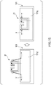
- a current Ir which contributes for radiation easily flows in the upper section of the split-ring resonator 21 in comparison with another case where it is not provided to an opening (in the case of the split-ring resonator 21 illustrated in Fig. 13 ). Accordingly, in the split-ring resonator 21 illustrated in Fig. 12 , because the ground terminal 14 is located on the upper section, the current Ir easily flows into another conductor through the ground terminal 14. As a result, the radiation property of the split-ring resonator 21 can be improved.
- the connection is made so that the split-ring resonator is accommodated within the opening. Accordingly, in the split-ring resonator 21 illustrated in Fig. 12 , the current Ir in the upper section of the split-ring resonator 21 can flow on a side of the ground pattern 101g of the board 101 through the ground terminal 14 without changing its direction. Therefore, the radiation property of the split-ring resonator 21 can be further improved.
- a split-ring resonator 31 is based on the split-ring resonator 21 while comprising a second ground terminal which is separated from a ground pattern, and the first ground terminal is located at a first corner of the split-ring resonator 31.
- the second ground terminal is located on a section where the split exists as viewed from the straight-line L and is located at a second corner of the split-ring resonator.
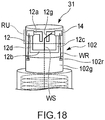
- Figs. 16, 17 and 18 are figures showing examples of the split-ring resonator 31 according to an aspect of the present disclosure.
- the split-ring resonator 31 may comprise the ground terminals 14 located at positions of two corners (two parts including the intersection of the first conductor 12a and the third conductor 12c, and the intersection of the first conductor 12a and the fourth conductor 12d) of the upper section RU of the split-ring resonator 31, respectively.
- a board according to an aspect of the present disclosure comprises a terminal configured to be connected to the ground terminal, which is separated from a ground pattern, of the split-ring resonator 31 according to an aspect of the present disclosure.
- Figs. 16 and 17 are figures showing examples of the board 101 according to an aspect of the present disclosure.
- the split-ring resonator 31 may comprise the ground terminals 14 located at the positions of the two corners (each of the intersection of the first conductor 12a and the third conductor 12c and the intersection of the first conductor 12a and the fourth conductor 12d) of the upper section RU of the split-ring resonator 31, respectively.
- a connector according to an aspect of the present disclosure comprises a terminal configured to be connected to the ground terminal, which is separated from a ground pattern, of the split-ring resonator 31 according to an aspect of the present disclosure.
- Fig. 18 is a figure showing an example of the connector 102 according to an aspect of the present disclosure.
- the split-ring resonator 31 may comprise the ground terminals 14 located at the positions of the two corners (each of the intersection of the first conductor 12a and the third conductor 12c and the intersection of the first conductor 12a and the fourth conductor 12d) of the upper section RU of the split-ring resonator 31, respectively.
- the ground terminals 14 are located on the two corners of the upper section RU of the split-ring resonator 31 .
- the current Ir further easily flows along a side in comparison with the split-ring resonator 21 illustrated in Figs. 12 , 13 and 14 .
- the radiation property of the split-ring resonator 31 can be further improved.
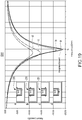
- Fig. 19 shows frequency characteristics of return loss of each split-ring resonator under the same condition.
- the curve a shows a return loss curve of the split-ring resonator 31 illustrated in Fig. 15 .
- the curve b shows a return loss curve of the split-ring resonator 21 illustrated in Fig. 12 .
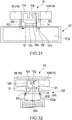
- the curve c shows a return loss curve of a split-ring resonator 51 according to a seventh embodiment lately illustrated in Fig. 21 .
- the curve d is a return loss curve of a reference example of a split-ring resonator which is based on a split-ring resonator 41 described later, and in which the ground terminal 14 is not provided while only a ground terminal 44 is provided. As shown in Fig.
- return losses at resonance frequency f0 decrease in the order of the curve d, the curve c, the curve b and the curve a.
- the return loss property of the curve a is closest to the return loss property in a case where a split-ring resonator is integrally formed with a circuit board (in a case of an integral board).
- the split-ring resonator 41 is based on the split-ring resonator 21 or the split-ring resonator 31 while comprising a third ground terminal which is separated from a ground pattern, and the third ground terminal is located on a section where the split does not exist as viewed from the straight-line L.
- Figs. 20, 21 and 22 are figures showing examples of the split-ring resonator 41 according to an aspect of the present disclosure.
- the split-ring resonator 41 comprises the ground terminals 14 located on the upper section RU of the split-ring resonator 41.
- a position of each conductor of the third conductor 12c and the fourth conductor 12d may be provided with one of the ground terminals 14.
- the split-ring resonator 41 may further comprise the ground terminal 44 located on the lower section RD of the split-ring resonator 41.
- the ground terminal 44 may be provided at a position of the second conductor 12b.
- the ground terminal 44 may be connected to the second conductor 12b.
- the ground terminal 44 may be connected to the ground pattern 101g via the solder SR.
- a board according to an aspect of the present disclosure comprises a terminal configured to be connected to the ground terminal, which is separated from a ground pattern, of the split-ring resonator 41 according to an aspect of the present disclosure.
- Figs. 20 and 21 are figures showing examples of the board 101 according to an aspect of the present disclosure.
- the split-ring resonator 41 may further comprise the ground terminal 44 located on the lower section RD of the split-ring resonator 41.
- the ground terminal 44 may be provided at a position of the second conductor 12b.
- the ground terminal 44 may be connected to the second conductor 12b.
- the ground terminal 44 may be connected to the ground pattern 101g via the solder SR.
- a connector according to an aspect of the present disclosure comprises a terminal configured to be connected to the ground terminal, which is separated from a ground pattern, of the split-ring resonator 41 according to an aspect of the present disclosure.
- Fig. 22 is a figure showing an example of the connector 102 according to an aspect of the present disclosure.
- the split-ring resonator 41 comprises the ground terminals 14 located on the upper section RU of the split-ring resonator 41.
- a position of each conductor of the third conductor 12c and the fourth conductor 12d may be provided with one of the ground terminals 14.
- the split-ring resonator 41 further comprises the ground terminal 44 located on the lower section RD of the split-ring resonator 41.
- the ground terminal 44 may be provided at a position of the second conductor 12b.
- the ground terminal 44 may be connected to the second conductor 12b.
- the ground terminal 44 may be electrically connected with the ground pattern 101g via the wire WR by soldering, pressure joining, etc.
- the ground terminal 44 may be applied to the split-ring resonator illustrated in Fig. 18 .
- the ground terminal 44 may be applied to the split-ring resonator illustrated in Fig. 14 .
- the ground terminal 44 for grounding of the feed current is provided on the lower section of the split-ring resonator 41.
- a feeding point is located on a side of the upper section (on the first conductor 12a including the split portion 12g), and that the feeding wire WS, which is connected to the feeding point, extends to the lower section of the split-ring resonator 41 through the opening located inside the ring of the split-ring resonator 41.
- a return current Ig of a fed current Is is not diverted to the ground terminal 14 of the upper section but can flow from the split-ring resonator 41 directly to the ground pattern 101g.
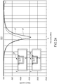
- the split-ring resonator 41 illustrated in Fig. 20 has less change in impedance and makes it easier to obtain matching in comparison with the split-ring resonator 21 illustrated in Fig. 12 . Therefore, as shown in Fig. 24 , the return loss at resonance frequency f0 of the split-ring resonator 41 illustrated in Fig. 20 is small in comparison with the split-ring resonator 21 illustrated in Fig. 12 .
- the curve a' and the curve b' show frequency characteristics of return loss of the split-ring resonator 41 and the split-ring resonator 21, respectively, under conditions different from those about Fig. 19 .
- the split-ring resonator 51 is based on the split-ring resonator 21 while a first ground terminal is located on a section where the split of the split-ring resonator does not exist as viewed from the straight-line L.
- the point C exists, the point C being a center of a ring of the split-ring resonator.
- the straight-line L is perpendicular to the line segment m which connects the point C and the split to each other (see Fig. 1 ).
- Figs. 25, 26 and 27 are figures showing examples of the split-ring resonator 51 according to an aspect of the present disclosure.
- the split-ring resonator 51 may comprise the ground terminal 14 located on the lower section RD of the split-ring resonator 51.
- the ground terminals 14 may be provided at positions of two corners (each of the intersection of the second conductor 12b and the third conductor 12c and the intersection of the second conductor 12b and the fourth conductor 12d) of the lower section RD of the split-ring resonator 51, respectively.
- the ground terminals 14 are provided on the two corners of the lower section RD of the split-ring resonator 51, respectively, they may be provided on any positions of the lower section RD of the split-ring resonator 51.
- the ground terminals 14 may be provided at positions of the second conductor 12b.
- the ground terminals 14 may be provided at a position of each conductor of the third conductor 12c and the fourth conductor 12d, respectively.
- a board according to an aspect of the present disclosure comprises a terminal configured to be connected to the ground terminal, which is separated from a ground pattern, of the split-ring resonator 51 according to an aspect of the present disclosure.
- Figs. 25 and 26 are figures showing examples of the board 101 according to an aspect of the present disclosure.
- the split-ring resonator 51 may be provided adjacent to an edge of the board 101.
- the split-ring resonator 51 may be provided so that the separation direction of the split portion 12g is aligned with a direction along which the adjacent edge of the board 101 extends.
- a connector according to an aspect of the present disclosure comprises a terminal configured to be connected to the ground terminal, which is separated from a ground pattern, of the split-ring resonator 51 according to an aspect of the present disclosure.
- Fig. 27 is a figure showing an example of the connector 102 according to an aspect of the present disclosure.
- the split-ring resonator 51 is provided to the connector 102 to be adjacent to the ground pattern 102g.
- the split-ring resonator 51 may be provided so that the separation direction of the split portion 12g is aligned with the radial direction of the connector 102.
- the ground terminals 14 may be connected to the ground pattern 102g via the wires WR.
- the split portion 12g is directed to a direction different from another direction along which the ground pattern 101g' of the board 101 is located.
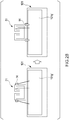
- the split-ring resonator 51 having the ground terminal 14 located on the lower section as illustrated in Fig. 26 can be connected to the ground pattern 101g' by a distance shorter than that of the split-ring resonator 21 illustrated in Fig. 13 . Therefore, the split-ring resonator 51 illustrated in Fig. 26 is more easily connected to the board 101 than the split-ring resonator 21 illustrated in Fig. 13 because of its structure.
- the split portion 12g is directed to a direction different from another direction along which the ground pattern 102g of the connector 102 is located.
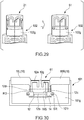
- the split-ring resonator 51 having the ground terminals located on the lower section as illustrated in Fig. 27 can be connected to the ground pattern 102g by a distance shorter than that of the split-ring resonator 21 illustrated in Fig. 14 . Therefore, the split-ring resonator 51 illustrated in Fig. 27 is more easily connected to the connector 102 than the split-ring resonator 21 illustrated in Fig. 14 because of its structure.
- a split-ring resonator 61 is based on the split-ring resonator 51 while comprising a radiation conductor.
- Figs. 30 , 31 and 32 are figures showing examples of the split-ring resonator 61 according to an aspect of the present disclosure.
- the split-ring resonator 61 may comprise radiation conductors 16.
- the split-ring resonator 61 may comprise a pair of radiation conductors 16 (a radiation conductor 16R and a radiation conductor 16L) which are apart from each other and face each other in the separation direction of the split portion 12g.
- the radiation conductor 16R and the radiation conductor 16L may extend so as to be away from each other in the separation direction.
- each of the radiation conductor 16R and radiation conductor 16L may be formed of a metal plate having a plate-like shape extending in the separation direction.
- the radiation conductors 16 may be provided on the upper section RU of the split-ring resonator 61.
- the radiation conductor 16R may be connected to the third conductor 12c.
- the radiation conductor 16L may be connected to the fourth conductor 12d.
- an end of each of the radiation conductor 16R and the radiation conductor 16L, which is connected to the split-ring 12, may further extend in a direction intersecting with a plane in which the ground pattern 101g extends so that the radiation conductor 16R and the radiation conductor 16L are not brought into contact with the ground pattern 101g.
- a board according to an aspect of the present disclosure comprises a terminal configured to be connected to the ground terminal, which is separated from a ground pattern, of the split-ring resonator 61 according to an aspect of the present disclosure.
- Figs. 30 and 31 are figures showing examples of the board 101 according to an aspect of the present disclosure.
- the split-ring resonator 61 may be provided adjacent to an edge of the board 101.
- the split-ring resonator 61 may be provided so that the separation direction of the split portion 12g is aligned with a direction along which the adjacent edge of the board 101 extends.
- a connector according to an aspect of the present disclosure comprises a terminal configured to be connected to the ground terminal, which is separated from a ground pattern, of the split-ring resonator 61 according to an aspect of the present disclosure.
- Fig. 32 is a figure showing an example of the connector 102 according to an aspect of the present disclosure.
- the split-ring resonator 61 may be provided to the connector 102 to be adjacent to the ground pattern 102g.
- the split-ring resonator 61 may be provided so that the separation direction of the split portion 12g is aligned with the radial direction of the connector 102.
- the ground terminals 14 may be connected to the ground pattern 102g via the wires WR.
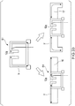
- the current Ir which contributes for radiation tends to flow in the separation direction of the split portion 12g. Accordingly, as shown in the lower left of Fig. 33 , since the split-ring resonator 61 illustrated in Fig. 30 comprises the radiation conductors 16 extending in the separation direction, the current Ir flows onto the radiation conductors 16. Therefore, the split-ring resonator 61 illustrated in Fig. 30 has an improved radiation property in comparison with the split-ring resonator 51 illustrated in Fig. 25 . Moreover, for example, as shown in the lower right of Fig.
- the split-ring resonator 61 may comprise L-like shaped radiation conductors 17 as radiation conductors, the radiation conductor 17 extending in the separation direction to an end and then extending from the end in a direction intersecting with the separation direction along a plane in which the split-ring resonator 61 extends.
- the comparison of the split-ring resonator 61 illustrated in Fig. 31 with the split-ring resonator 51 illustrated in Fig. 26 comes to a similar conclusion.
- the comparison of the split-ring resonator 61 illustrated in Fig. 32 with the split-ring resonator 51 illustrated in Fig. 27 comes to a similar conclusion.
- a split-ring resonator 71 is based on the split-ring resonator 21 while all ground terminals including the previously described first ground terminal are located on one of opposite sections across the straight-line M.
- the straight-line M is a straight-line including a line segment which connects the point C and the split of the split-ring resonator to each other, the point C being a center of a ring of the split-ring resonator (see Fig. 1 ).
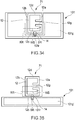
- Figs. 34, 35 and 36 are figures showing examples of the split-ring resonator 71 according to an aspect of the present disclosure.
- the split-ring resonator 71 may comprise the ground terminal 14 located either on the right section RR or on the left section RL of the split-ring resonator 71.
- the ground terminal 14 may be provided on the right section RR of the split-ring resonator 71.
- the ground terminal 14 may be provided at a position of the third conductor 12c.
- the ground terminal 14 may be connected to the third conductor 12c.
- the split-ring resonator 71 is provided to the opening 101a so that the separation direction of the split portion 12g intersects with the direction along which the opening 101a is widen.
- the ground terminal 14 may be located in the opening 101a and may be connected to an edge of the ground pattern 101g which extends in the direction along which the opening 101a is widen.
- the ground terminal 14 may be provided on the third conductor 12c, it may be provided at any position of either the right section RR or the left section RL of the split-ring resonator 71.
- the ground terminal 14 may be provided at a position of the first conductor 12a. In this case, the ground terminal 14 may be connected to the first conductor 12a.
- the ground terminal 14 may be provided at a position of the second conductor 12b. In this case, the ground terminal 14 may be connected to the second conductor 12b.
- a board according to an aspect of the present disclosure comprises a terminal configured to be connected to the ground terminal, which is separated from a ground pattern, of the split-ring resonator 71 according to an aspect of the present disclosure.
- Figs. 34 and 35 are figures showing examples of the board 101 according to an aspect of the present disclosure.
- the split-ring resonator 71 may be provided adjacent to an edge of the board 101.
- the split-ring resonator 71 may be provided so that a cutting direction of the split portion 12g is aligned with a direction along which the adjacent edge of the board 101 extends.
- a connector according to an aspect of the present disclosure comprises a terminal configured to be connected to the ground terminal, which is separated from a ground pattern, of the split-ring resonator 71 according to an aspect of the present disclosure.
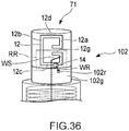
- Fig. 36 is a figure showing an example of the connector 102 according to an aspect of the present disclosure.
- the split-ring resonator 71 may be provided to the connector 102 to be adjacent to the ground pattern 102g.
- the split-ring resonator 71 may be provided so that the cutting direction of the split portion 12g is aligned with the radial direction of the connector 102.
- the ground terminal 14 may be connected to the ground pattern 102g via the wire WR.
- the split-ring resonator 71 illustrated in Fig. 34 can be easily connected to the ground pattern 101g' when the ground terminal 14 is provided on either the right section RR or the left section RL of the split-ring resonator 71.
- the connection is made easier in a case where the ground terminal 14 is provided on the right section RR of the split-ring resonator 71 in comparison with another case where the ground terminal 14 is provided on the left section RL (a comparative example illustrated in the left of Fig. 37 ).
- a split-ring resonator 81 is based on the split-ring resonator 71 while the first ground terminal is located on a section where the split exists as viewed from the straight-line L. On the straight-line L, the point C exists, and the straight-line L is perpendicular to the line segment m which connects the point C and the split to each other.
- Figs. 38, 39 and 40 are figures showing examples of the split-ring resonator 81 according to an aspect of the present disclosure.
- the split-ring resonator 81 may comprise the ground terminal 14 located on either the right section RR or the left section RL of the split-ring resonator 81, for example, on the right section RR of the split-ring resonator 81.
- the ground terminal 14 may be provided on the right section RR of the split-ring resonator 81 and on the upper section RU of the split-ring resonator 81.
- a board according to an aspect of the present disclosure comprises a terminal configured to be connected to the ground terminal, which is separated from a ground pattern, of the split-ring resonator 81 according to an aspect of the present disclosure.
- Figs. 38 and 39 are figures showing examples of the board 101 according to an aspect of the present disclosure.
- the split-ring resonator 81 may be provided adjacent to an edge of the board 101.
- the split-ring resonator 81 may be provided so that the cutting direction of the split portion 12g is aligned with a direction along which the adjacent edge of the board 101 extends.
- a connector according to an aspect of the present disclosure comprises a terminal configured to be connected to the ground terminal, which is separated from a ground pattern, of the split-ring resonator 81 according to an aspect of the present disclosure.
- Fig. 40 is a figure showing an example of the connector 102 according to an aspect of the present disclosure.
- the split-ring resonator 81 may be provided to the connector 102 to be adjacent to the ground pattern 102g.
- the split-ring resonator 81 may be provided so that the cutting direction of the split portion 12g is aligned with the radial direction of the connector 102.
- the ground terminal 14 may be connected to the ground pattern 102g via the wire WR.
- the comparison of the split-ring resonator 81 illustrated in Fig. 39 with the split-ring resonator 71 illustrated in Fig. 35 comes to a similar conclusion. Also, the comparison of the split-ring resonator 81 illustrated in Fig. 40 with the split-ring resonator 71 illustrated in Fig. 36 comes to a similar conclusion.
- a split-ring resonator 91 is based on the split-ring resonator 71 or the split-ring resonator 81 while comprising a radiation conductor located on a section where the first conductor does not exist as viewed from the straight-line M.
- Figs. 41 , 42 and 43 are figures showing examples of the split-ring resonator 91 according to an aspect of the present disclosure.
- the split-ring resonator 91 may comprise a radiation conductor 16'.
- the split-ring resonator 91 may comprise the radiation conductor 16' located on one of the right section RR and the left section RL of the split-ring resonator 91, the one of the right section RR and the left section RL being located opposite to a remaining one where the ground terminal 14 is provided.
- the split-ring resonator 91 may comprise the radiation conductor 16' located on the left section RL of the split-ring resonator 91 and located on the upper section RU of the split-ring resonator 91.
- the radiation conductor 16' may be connected to the fourth conductor 12d.
- the radiation conductor 16' may extend in the separation direction from an end connected to the split-ring 12 so as to be away from the fourth conductor 12d.
- the radiation conductor 16' may be formed of a metal plate having a plate-like shape extending from the split-ring 12 in the separation direction.
- the ground terminal 14 may be provided at any position of either the right section RR or the left section RL of the split-ring resonator 91.
- the ground terminal 14 may be provided on either the right section RR or the left section RL of the split-ring resonator 91, for example, on the lower section RD of the split-ring resonator 91.
- a board according to an aspect of the present disclosure comprises a terminal configured to be connected to the ground terminal, which is separated from a ground pattern, of the split-ring resonator 91 according to an aspect of the present disclosure.
- Figs. 41 and 42 are figures showing examples of the board 101 according to an aspect of the present disclosure.
- the split-ring resonator 91 may be provided adjacent to an edge of the board 101.
- the split-ring resonator 91 may be provided so that the cutting direction of the split portion 12g is aligned with a direction along which the adjacent edge of the board 101 extends.
- a connector according to an aspect of the present disclosure comprises a terminal configured to be connected to the ground terminal, which is separated from a ground pattern, of the split-ring resonator 91 according to an aspect of the present disclosure.
- Fig. 43 is a figure showing an example of the connector 102 according to an aspect of the present disclosure.
- the split-ring resonator 91 may be provided to the connector 102 to be adjacent to the ground pattern 102g.
- the split-ring resonator 91 may be provided so that the cutting direction of the split portion 12g is aligned with the radial direction of the connector 102.
- the ground terminal 14 may be connected to the ground pattern 102g via the wire WR.
- the current Ir which contributes for radiation tends to flow in the separation direction of the split portion 12g. Accordingly, as shown in the lower left of Fig. 44 , since the split-ring resonator 91 illustrated in Fig. 41 comprises the radiation conductor 16' extending in the separation direction, the current Ir flows onto the radiation conductor 16'. Therefore, the split-ring resonator 91 illustrated in Fig. 41 has an improved radiation property in comparison with the split-ring resonator 81 illustrated in Fig. 38 . Moreover, as shown in the lower right of Fig.
- the split-ring resonator 91 may comprise an L-like shaped radiation conductor 17' as a radiation conductor, the radiation conductor 17' extending in the separation direction to an end and then extending from the end in a direction intersecting with the separation direction along a plane in which the split-ring resonator 91 extends.
- the comparison of the split-ring resonator 91 illustrated in Fig. 42 with the split-ring resonator 81 illustrated in Fig. 39 comes to a similar conclusion.
- the comparison of the split-ring resonator 91 illustrated in Fig. 43 with the split-ring resonator 81 illustrated in Fig. 40 comes to a similar conclusion.
- the ground terminal 14 of the split-ring resonator may be connected by a lead 92 as shown in Fig. 45 .
- the ground terminal 14 of the split-ring resonator may be connected by the lead 92 as shown in Fig. 46 .
- the ground terminal 14 of the split-ring resonator may be connected by the lead 92 as shown in Fig. 47 .
- the ground terminal 14 of the split-ring resonator may be connected by the lead 92 as shown in Fig. 48 .
- the feeding wire WS of the split-ring resonator may be connected by a lead 93.
- the ground terminal 14 of the split-ring resonator may be connected by the lead 92.
- the feeding wire WS of the split-ring resonator may be connected by the lead 93.
- the ground terminal 14 of the split-ring resonator may be connected by the lead 92 as shown in Fig. 50 .
- the ground terminal 14 and the feeding wire WS of the split-ring resonator may be connected by the lead 92 and the lead 93, respectively.
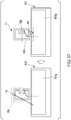
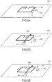
- the ground terminal 14 of the split-ring resonator may be connected by the lead 92 so that the board 101 and the split-ring resonator have a gap G as shown in Fig. 52 .
- the ground terminal 14 of the split-ring resonator may be connected by the lead 92 so that the board 101 and the split-ring resonator have the gap G as shown in Fig. 53 .
- the ground terminal 14 of the split-ring resonator may be connected by the lead 92 so that the board 101 and the split-ring resonator have the gap G as shown in Fig. 54 .
- the ground terminal 14 and the feeding wire WS of the split-ring resonator may be connected by the lead 92 and the lead 93, respectively, so that the board 101 and the split-ring resonator have the gap G.
- the ground terminal 14 and the feeding wire WS of the split-ring resonator may be connected by the lead 92 and the lead 93, respectively, so that the board 101 and the split-ring resonator.
- the ground terminal 14 of the split-ring resonator may be connected to the board 101 by the lead 92 as shown in Fig. 57 .
- the ground terminal 14 of the split-ring resonator may be connected to the board 101 the lead 92 as shown in Fig. 58 .
Landscapes
- Physics & Mathematics (AREA)
- Electromagnetism (AREA)
- Control Of Motors That Do Not Use Commutators (AREA)
- Coupling Device And Connection With Printed Circuit (AREA)
- Piezo-Electric Or Mechanical Vibrators, Or Delay Or Filter Circuits (AREA)
Abstract
Description
- This invention relates to a split-ring resonator, a board and a connector.
- An antenna with a split-ring resonator is known as a compact antenna used in a wireless communication device. For example,
Patent Document 1 discloses a wireless communication device comprising a split-ring resonator. - Patent Document 1:
WO 2013/027824 - The split-ring resonator of
Patent Document 1 is formed directly on a board while being connected to a ground pattern. Therefore, the split-ring resonator according to the aspect disclosed inPatent Document 1 neither can be distributed as a single component nor can be flexibly combined with the other component in accordance with design requirements. Thus, according to the aspect disclosed inPatent Document 1, the split-ring resonator cannot be used as a component. - The object of an aspect of the present disclosure is to provide a split-ring resonator, a board and a connector for solving one or more of the problems described above.
- A split-ring resonator according to an aspect of the present disclosure comprises a first ground terminal which is separated from a ground pattern.
- A board according to an aspect of the present disclosure comprises a terminal configured to be connected to a ground terminal, which is separated from a ground pattern, of a split-ring resonator according to an aspect of the present disclosure.
- A connector according to an aspect of the present disclosure comprises a terminal configured to be connected to a ground terminal, which is separated from a ground pattern, of a split-ring resonator according to an aspect of the present disclosure.
- Various aspects of the present disclosure enable a split-ring resonator to be used as a component.
-
-
Fig. 1 is a plan view showing a split-ring resonator according to an aspect of the present disclosure. -
Fig. 2 is a plan view showing a split-ring resonator according to an aspect of the present disclosure. -
Fig. 3 is a plan view showing a split-ring resonator according to an aspect of the present disclosure. -
Fig. 4 is a perspective view showing a split-ring resonator according to an aspect of the present disclosure. -
Fig. 5 is a perspective view showing a split-ring resonator according to an aspect of the present disclosure. -
Fig. 6 is a plan view showing a split-ring resonator according to an aspect of the present disclosure. -
Fig. 7 is a plan view showing a board according to an aspect of the present disclosure. -
Fig. 8 is a plan view showing a board according to an aspect of the present disclosure. -
Fig. 9 is a perspective view showing a connector according to an aspect of the present disclosure. -
Fig. 10 is a view for explaining about a connection between a connector and a main circuit board according to an aspect of the present disclosure. -
Fig. 11 is a view for explaining about a split-ring resonator according to an aspect of the present disclosure. -
Fig. 12 is a plan view showing a split-ring resonator according to an aspect of the present disclosure. -
Fig. 13 is a plan view showing a split-ring resonator according to an aspect of the present disclosure. -
Fig. 14 is a perspective view showing a split-ring resonator according to an aspect of the present disclosure. -
Fig. 15 is a view for comparing currents in split-ring resonators according to an aspect of the present disclosure. -
Fig. 16 is a plan view showing a split-ring resonator according to an aspect of the present disclosure. -
Fig. 17 is a plan view showing a split-ring resonator according to an aspect of the present disclosure. -
Fig. 18 is a perspective view showing a split-ring resonator according to an aspect of the present disclosure. -
Fig. 19 is a graph showing return loss properties of split-ring resonators according to an aspect of the present disclosure. -
Fig. 20 is a plan view showing a split-ring resonator according to an aspect of the present disclosure. -
Fig. 21 is a plan view showing a split-ring resonator according to an aspect of the present disclosure. -
Fig. 22 is a perspective view showing a split-ring resonator according to an aspect of the present disclosure. -
Fig. 23 is a view for comparing currents in split-ring resonators according to an aspect of the present disclosure. -
Fig. 24 is a graph showing return loss properties of split-ring resonators according to an aspect of the present disclosure. -
Fig. 25 is a plan view showing a split-ring resonator according to an aspect of the present disclosure. -
Fig. 26 is a plan view showing a split-ring resonator according to an aspect of the present disclosure. -
Fig. 27 is a perspective view showing a split-ring resonator according to an aspect of the present disclosure. -
Fig. 28 is a view for comparing connection configurations each of which is between a split-ring resonator and a board according to an aspect of the present disclosure. -
Fig. 29 is a view for comparing connection configurations each of which is between a split-ring resonator and a connector according to an aspect of the present disclosure. -
Fig. 30 is a plan view showing a split-ring resonator according to an aspect of the present disclosure. -
Fig. 31 is a plan view showing a split-ring resonator according to an aspect of the present disclosure. -
Fig. 32 is a perspective view showing a split-ring resonator according to an aspect of the present disclosure. -
Fig. 33 is a view for explaining about currents in radiating conductors. -
Fig. 34 is a plan view showing a split-ring resonator according to an aspect of the present disclosure. -
Fig. 35 is a plan view showing a split-ring resonator according to an aspect of the present disclosure. -
Fig. 36 is a perspective view showing a split-ring resonator according to an aspect of the present disclosure. -
Fig. 37 is a view for comparing connection configurations each of which is between a split-ring resonator and a board according to an aspect of the present disclosure. -
Fig. 38 is a plan view showing a split-ring resonator according to an aspect of the present disclosure. -
Fig. 39 is a plan view showing a split-ring resonator according to an aspect of the present disclosure. -
Fig. 40 is a perspective view showing a split-ring resonator according to an aspect of the present disclosure. -
Fig. 41 is a plan view showing a split-ring resonator according to an aspect of the present disclosure. -
Fig. 42 is a plan view showing a split-ring resonator according to an aspect of the present disclosure. -
Fig. 43 is a perspective view showing a split-ring resonator according to an aspect of the present disclosure. -
Fig. 44 is a plan view showing currents in radiating conductors according to an aspect of the present disclosure. -
Fig. 45 is a perspective view showing an example configuration for connecting a split-ring resonator according to an embodiment to a board via a lead. -
Fig. 46 is a perspective view showing another example configuration for connecting a split-ring resonator according to an embodiment to a board via a lead. -
Fig. 47 is a perspective view showing still another example configuration for connecting a split-ring resonator according to an embodiment to a board via a lead. -
Fig. 48 is a perspective view showing yet another example configuration for connecting a split-ring resonator according to an embodiment to a board via a lead. -
Fig. 49 is a perspective view showing further example configuration for connecting a split-ring resonator according to an embodiment to a board via a lead. -
Fig. 50 is a perspective view showing still further example configuration for connecting a split-ring resonator according to an embodiment to a board via a lead. -
Fig. 51 is a perspective view showing yet further example configuration for connecting a split-ring resonator according to an embodiment to a board via a lead. -
Fig. 52 is a perspective view showing yet further example configuration for connecting a split-ring resonator according to an embodiment to a board via a lead. -
Fig. 53 is a perspective view showing yet further example configuration for connecting a split-ring resonator according to an embodiment to a board via a lead. -
Fig. 54 is a perspective view showing yet further example configuration for connecting a split-ring resonator according to an embodiment to a board via a lead. -
Fig. 55 is a perspective view showing yet further example configuration for connecting a split-ring resonator according to an embodiment to a board via a lead. -
Fig. 56 is a perspective view showing yet further example configuration for connecting a split-ring resonator according to an embodiment to a board via a lead. -
Fig. 57 is a perspective view showing yet further example configuration for connecting a split-ring resonator according to an embodiment to a board via a lead. -
Fig. 58 is a perspective view showing yet further example configuration for connecting a split-ring resonator according to an embodiment to a board via a lead. - Various aspects according to the present disclosure are merely examples and are not intended to limit technical features of the invention described in Claims.
- A split-
ring resonator 11 according to an aspect of the present disclosure comprises aground terminal 14 which is separated from a ground pattern. -
Figs. 1, 2 and3 are figures showing examples of the split-ring resonator 11 according to an aspect of the present disclosure. - For example, a center of a ring of the split-
ring resonator 11 will be referred to as a point C. For example, a line segment which connects a split of the split-ring resonator 11 and the point C to each other will be referred to as a line segment m. For example, a straight-line which includes the line segment m will be referred to as a straight-line M. For example, another straight-line which is perpendicular to the line segment m (or the straight-line M) and passes through the point C will be referred to as a straight-line L. Thus, on the straight-line L, the point C exists. For example, a direction in which the straight-line M extends will be referred to as the Y-axis direction. For example, a direction in which the straight-line L extends will be referred to as the X-axis direction. - For example, the split-
ring resonator 11 may comprise a split-ring 12. For example, the split-ring 12 may be shaped into a C-like shape extending along a rectangular ring, the C-like shape being formed of: asplit portion 12g; afirst conductor 12a which extends in the X-axis direction while sandwiching thesplit portion 12g therebetween; asecond conductor 12b which extends in the X-axis direction; athird conductor 12c which extends in the Y-axis direction; and afourth conductor 12d which extends in the Y-axis direction. For example, the split-ring 12 may have a shape which extends along one of various rings including a circular ring, an elliptical ring, a track-shaped ring and any other rings. For example, the split-ring 12 may be formed of a metal plate. - For example, the split-
ring resonator 11 may comprise theground terminal 14 separated from a ground pattern. For example, the split-ring resonator 11 may comprise not only theground terminal 14 but also a plurality of theground terminals 14 each separated from a ground pattern. For example, theground terminal 14 may have any structure, provided that the structure is electrically connectable with a ground pattern. For example, theground terminal 14 may be configured to be electrically connected with a ground pattern via soldering, pressure joining, a connector, a pin, etc. For example, theground terminal 14 may be a land pattern as shown inFig. 1 . For example, theground terminal 14 may be a pattern which projects outward from the outer circumference of the split-ring resonator 11 as shown inFig. 2 . For example, theground terminal 14 may be an exposed pattern which is formed by partially removing a coat of the split-ring resonator 11 as shown inFig. 3 . For example, not limited to theground terminal 14 but any one of the ground terminals of the present disclosure may have any structure, provided that the structure is electrically connectable with a ground pattern. For example, theground terminal 14 may be formed of a metal plate. -
Figs. 4 ,5 and 6 are figures showing examples of the split-ring resonator 11 according to an aspect of the present disclosure.Figs. 4 ,5 and 6 show a structure in which the split-ring resonator 11 comprises the oneground terminal 14. However, the split-ring resonator 11 may comprise two or more of the ground terminals. - For example, as shown in
Fig. 4 , the split-ring resonator 11 may comprise the split-ring 12, theground terminal 14 and a feedingterminal 13. For example, the feedingterminal 13 may be formed of a wire and a metal plate. For example, the feedingterminal 13 may be a terminal for supplying radio frequency (RF) signals to the split-ring 12. For example, the feedingterminal 13 may be connected to the split-ring 12. For example, the feedingterminal 13 may be connected to a transmission line. For example, the feedingterminal 13 may be connected to thefirst conductor 12a. - For example, as shown in
Fig. 5 , the split-ring resonator 11 may comprise the split-ring 12, theground terminal 14, the feedingterminal 13 and achip body 15. - For example, as shown in
Fig. 6 , the split-ring resonator 11 may comprise the split-ring 12, theground terminal 14, the feedingterminal 13 and a printed circuit board 15'. For example, as shown inFig. 6 , the split-ring 12, theground terminal 14 and the feedingterminal 13 are provided on one of surfaces of the printed circuit board 15'. For example, the printed circuit board 15' may have either a single-layer structure or a multi-layer structure. For example, when the printed circuit board 15' has a multi-layer structure, the split-ring 12, theground terminal 14 and the feedingterminal 13 may be provided on one of layers thereof. - A board according to an aspect of the present disclosure comprises a terminal configured to be connected to a ground terminal, which is separated from a ground pattern, of a split-ring resonator according to an aspect of the present disclosure.
-
Figs. 7 and 8 are figures showing examples of aboard 101 according to an aspect of the present disclosure. - For example, the
board 101 may comprise aground pattern 101g having a rectangular outline. For example, theboard 101 may comprise areception terminal 101r. For example, thereception terminal 101r may be a terminal configured to be connected to a ground terminal, which is separated from a ground pattern, of a split-ring resonator according to an aspect of the present disclosure. For example, as shown inFig. 7 , theboard 101 may comprise anopening 101a which corresponds to a shape and a size of a split-ring resonator according to an aspect of the present disclosure. In this case, for example, as shown inFig. 7 , an antenna may be formed by accommodating a split-ring resonator according to an aspect of the present disclosure in theopening 101a and by connecting thereception terminal 101r to a ground terminal, which is separated from a ground pattern, of the split-ring resonator according to an aspect of the present disclosure. For example, as shown inFig. 8 , theboard 101 may comprise no opening which corresponds to a shape and a size of a split-ring resonator according to an aspect of the present disclosure. In this case, for example, as shown inFig. 8 , an antenna may be formed by arranging a split-ring resonator according to an aspect of the present disclosure to be adjacent to a side or an edge of aground pattern 101g' and by connecting thereception terminal 101r to a ground terminal, which is separated from a ground pattern, of the split-ring resonator according to an aspect of the present disclosure. - A connector according to an aspect of the present disclosure comprises a terminal configured to be connected to a ground terminal, which is separated from a ground pattern, of a split-ring resonator according to an aspect of the present disclosure.
-
Figs. 9 and 10 are figures showing examples of aconnector 102 according to an aspect of the present disclosure. - For example, the
connector 102 may comprise aground pattern 102g. For example, theconnector 102 may comprise areception terminal 102r. For example, theconnector 102 may comprise afeeding pattern 102s. For example, theconnector 102 may be shaped in a cylindrical shape whose axial direction is an extending direction of thefeeding pattern 102s, and whose circumference surface is formed of theground pattern 102g, so that theconnector 102 may be formed as a coaxial connector having a central wire of the connector formed of thefeeding pattern 102s and having an outer conductor of the connector formed of theground pattern 102g. - For example, the
ground pattern 102g may have a screw shape which is located at one of opposite ends of theconnector 102 in the axial direction and may be electrically and mechanically connectable with another ground pattern having a corresponding screw shape. For example, theconnector 102 may comprise adielectric cap 102c which is located at a remaining one of the opposite ends in the axial direction and is adjacent to theground pattern 102g, so that the split-ring resonator 11 may be accommodatable in thedielectric cap 102c. For example, the split-ring resonator 11 may be provided at the remaining one of the opposite ends of theconnector 102 in the axial direction to be adjacent to theground pattern 102g. For example, theground pattern 102g may be connected to theground terminal 14 via thereception terminal 102r, and thefeeding pattern 102s may be connected to the feedingterminal 13. - For example, the
connector 102 may be a female connector with theground pattern 102g having a female screw shape. For example, theconnector 102 may be connected to amain circuit board 103 having a male connector. For example, as shown inFig. 9 , the split-ring resonator 11 (ground terminal 14) may be connected to amain ground pattern 103g of themain circuit board 103 via theground pattern 102g. For example, theground pattern 102g may have either a female screw shape or a male screw shape. For example, as shown inFig. 10 , theground pattern 102g of theconnector 102 may have a male screw shape, and theconnector 102 may be connected to a main circuit board having a female connector. - When the
ground terminal 14 is connected with a ground pattern, a current in accordance with RF signals can flow between the feedingterminal 13 and theground terminal 14 of a split-ring resonator 21. Therefore, an antenna can be formed by combining the aforementioned split-ring resonator according to an aspect of the present disclosure to the aforementioned board according to an aspect of the present disclosure or the aforementioned connector according to an aspect of the present disclosure. Therefore, according to an aspect of the present disclosure described above, a split-ring resonator can be distributed as a single component and can be flexibly combined with the other component in accordance with design requirements. - The split-
ring resonator 21 according to an aspect of the present disclosure is based on the split-ring resonator 11 while a first ground terminal is located on a section where a split of the split-ring resonator exists as viewed from the straight-line L. On the straight-line L, the point C exists, the point C being a center of a ring of the split-ring resonator. The straight-line L is perpendicular to the line segment m which connects the point C and the split to each other. -
Figs. 11, 12 ,13 and 14 are figures showing examples of the split-ring resonator 21 according to an aspect of the present disclosure. - For example, each section of a split-ring resonator will be defined as follows.
- As shown in
Fig. 11 , a section where a split of a split-ring resonator is as viewed from the straight-line L is defined as an upper section RU of the split-ring resonator. For example, an upper half part of the split-ring 12 (i.e. a part formed of: thesplit portion 12g; thefirst conductor 12a; a part of thethird conductor 12c which is nearer to thefirst conductor 12a than to thesecond conductor 12b; and a part of thefourth conductor 12d which is nearer to thefirst conductor 12a than to thesecond conductor 12b) may be configured to be the upper section RU of the split-ring resonator. - As shown in
Fig. 11 , a section opposite to the section for the split of the split-ring resonator across the straight-line L is defined as a lower section RD of the split-ring resonator. For example, a lower half part of the split-ring 12 (i.e. a part formed of: thesecond conductor 12b; a part of thethird conductor 12c which is nearer to thesecond conductor 12b than to thefirst conductor 12a; and a part of thefourth conductor 12d which is nearer to thesecond conductor 12b than to thefirst conductor 12a) may be configured to be the lower section RD of the split-ring resonator. - As shown in
Fig. 11 , one of opposite sections of the split-ring resonator across the straight-line M (the right section inFig. 9 ) is defined as a right section RR. For example, a right half part of the split-ring 12 (i.e. a part formed of: thethird conductor 12c; a part of thefirst conductor 12a which is nearer to thethird conductor 12c than to thefourth conductor 12d; a part of thesplit portion 12g which is nearer to thethird conductor 12c than to thefourth conductor 12d; and a part of thesecond conductor 12b which is nearer to thethird conductor 12c than to thefourth conductor 12d) may be configured to be the right section RR of the split-ring resonator. - As shown in
Fig. 11 , a remaining one of the opposite sections across the straight-line M (the left section inFig. 9 ) is defined as a left section RL. For example, a left half part of the split-ring 12 (i.e. a part formed of: thefourth conductor 12d; a part of thefirst conductor 12a which is nearer to thefourth conductor 12d than to thethird conductor 12c; a part of thesplit portion 12g which is nearer to thefourth conductor 12d than to thethird conductor 12c; and a part of thesecond conductor 12b which is nearer to thefourth conductor 12d than to thethird conductor 12c) may be configured to be the left section RL of the split-ring resonator. - For example, the split-
ring resonator 21 may comprise theground terminal 14 located on the upper section RU of the split-ring resonator 21. For example, a position of each conductor of thethird conductor 12c and thefourth conductor 12d may be provided with one of theground terminals 14, respectively. For example, eachground terminal 14 may be connected to each conductor of thethird conductor 12c and thefourth conductor 12d, respectively. - For example, the split-
ring resonator 21 may be provided at a position of theopening 101a of theboard 101. For example, the split-ring resonator 21 may be provided in theopening 101a so that a separation direction of thesplit portion 12g is directed to a direction along which theopening 101a is widen. For example, the split-ring resonator 21 may be provided to theboard 101 so that the split-ring resonator 21 is accommodated within theopening 101a. Here, the direction along which theopening 101a is widen is defined as a direction along which one of the sides of the rectangular shape of theground pattern 101g extends, the one of the sides having a rectangular-shaped cut. - For example, each
ground terminal 14 may be electrically connected with theground pattern 101g via soldering, pressure joining, etc. For example, eachground terminal 14 may be connected to theground pattern 101g via solder SR. For example, thefirst conductor 12a may be connected to a feeding wire WS which supplies RF signals. - For example, a position of each conductor of the
third conductor 12c and thefourth conductor 12d may be provided at any position in the upper section RU of the split-ring resonator 21. For example, theground terminal 14 may be provided at a position of thefirst conductor 12a. In this case, theground terminal 14 may be connected to thefirst conductor 12a. For example, it may be connected to thethird conductor 12c or thefourth conductor 12d at a position which is nearer to thesplit portion 12g than to theground terminal 14. For example, the feeding wire WS may be connected to thesplit portion 12g. - A board according to an aspect of the present disclosure comprises a terminal configured to be connected to the ground terminal, which is separated from a ground pattern, of the split-
ring resonator 21 according to an aspect of the present disclosure. -
Figs. 12 and13 are figures showing examples of theboard 101 according to an aspect of the present disclosure. - For example, the split-
ring resonator 21 may comprise theground terminal 14 located on the upper section RU of the split-ring resonator 21. For example, a position of each conductor of thethird conductor 12c and thefourth conductor 12d is provided with one of theground terminals 14, respectively. Eachground terminal 14 may be connected to each conductor of thethird conductor 12c and thefourth conductor 12d, respectively. - For example, the split-
ring resonator 21 may be provided adjacent to an edge of theboard 101. For example, the split-ring resonator 21 may be provided so that the separation direction of thesplit portion 12g is aligned with a direction along which the adjacent edge of theboard 101 extends. For example, eachground terminal 14 may be electrically connected with theground pattern 101g' via a wire WR by soldering, pressure joining, etc. For example, the feeding wire WS and the wire WR may be realized by a central wire and an outer conductor of a connector. - For example, the
ground terminal 14 may be provided at any position in the upper section RU of the split-ring resonator 21. For example, theground terminal 14 may be provided at a position of thefirst conductor 12a. In this case, theground terminal 14 may be connected to thefirst conductor 12a. - A connector according to an aspect of the present disclosure comprises a terminal configured to be connected to the ground terminal, which is separated from a ground pattern, of the split-
ring resonator 21 according to an aspect of the present disclosure. -
Fig. 14 is a figure showing an example of theconnector 102 according to an aspect of the present disclosure. - For example, the split-
ring resonator 21 comprises theground terminal 14 located on the upper section RU of the split-ring resonator 21. According to the present embodiment, a position of each conductor of thethird conductor 12c and thefourth conductor 12d may be provided with one of theground terminals 14, respectively. For example, eachground terminal 14 may be connected to each conductor of thethird conductor 12c and thefourth conductor 12d, respectively. - For example, the split-
ring resonator 21 may be provided to theconnector 102. For example, the split-ring resonator 21 may be provided so that the separation direction of thesplit portion 12g is aligned with the radial direction of theconnector 102. For example, eachground terminal 14 may be electrically connected with theground pattern 102g via the wire WR by soldering, pressure joining, etc. - For example, it may be provided at any position in the upper section RU of the split-
ring resonator 21. For example, theground terminal 14 may be provided at a position of thefirst conductor 12a. In this case, theground terminal 14 may be connected to thefirst conductor 12a. - As shown in
Fig. 15 , in a case where the split-ring resonator 21 is provided to an opening (in the case of the split-ring resonator 21 illustrated inFig. 12 ), a current Ir which contributes for radiation easily flows in the upper section of the split-ring resonator 21 in comparison with another case where it is not provided to an opening (in the case of the split-ring resonator 21 illustrated inFig. 13 ). Accordingly, in the split-ring resonator 21 illustrated inFig. 12 , because theground terminal 14 is located on the upper section, the current Ir easily flows into another conductor through theground terminal 14. As a result, the radiation property of the split-ring resonator 21 can be improved. Moreover, in the case where the split-ring resonator 21 is provided to an opening, the connection is made so that the split-ring resonator is accommodated within the opening. Accordingly, in the split-ring resonator 21 illustrated inFig. 12 , the current Ir in the upper section of the split-ring resonator 21 can flow on a side of theground pattern 101g of theboard 101 through theground terminal 14 without changing its direction. Therefore, the radiation property of the split-ring resonator 21 can be further improved. - A split-
ring resonator 31 according to an aspect of the present disclosure is based on the split-ring resonator 21 while comprising a second ground terminal which is separated from a ground pattern, and the first ground terminal is located at a first corner of the split-ring resonator 31. The second ground terminal is located on a section where the split exists as viewed from the straight-line L and is located at a second corner of the split-ring resonator. -
Figs. 16, 17 and18 are figures showing examples of the split-ring resonator 31 according to an aspect of the present disclosure. - For example, the split-
ring resonator 31 may comprise theground terminals 14 located at positions of two corners (two parts including the intersection of thefirst conductor 12a and thethird conductor 12c, and the intersection of thefirst conductor 12a and thefourth conductor 12d) of the upper section RU of the split-ring resonator 31, respectively. - A board according to an aspect of the present disclosure comprises a terminal configured to be connected to the ground terminal, which is separated from a ground pattern, of the split-
ring resonator 31 according to an aspect of the present disclosure. -
Figs. 16 and 17 are figures showing examples of theboard 101 according to an aspect of the present disclosure. - For example, the split-
ring resonator 31 may comprise theground terminals 14 located at the positions of the two corners (each of the intersection of thefirst conductor 12a and thethird conductor 12c and the intersection of thefirst conductor 12a and thefourth conductor 12d) of the upper section RU of the split-ring resonator 31, respectively. - A connector according to an aspect of the present disclosure comprises a terminal configured to be connected to the ground terminal, which is separated from a ground pattern, of the split-
ring resonator 31 according to an aspect of the present disclosure. -
Fig. 18 is a figure showing an example of theconnector 102 according to an aspect of the present disclosure. - For example, the split-
ring resonator 31 may comprise theground terminals 14 located at the positions of the two corners (each of the intersection of thefirst conductor 12a and thethird conductor 12c and the intersection of thefirst conductor 12a and thefourth conductor 12d) of the upper section RU of the split-ring resonator 31, respectively. - Moreover, in the split-
ring resonator 31 illustrated inFigs. 16, 17 and18 , because theground terminals 14 are located on the two corners of the upper section RU of the split-ring resonator 31, the current Ir further easily flows along a side in comparison with the split-ring resonator 21 illustrated inFigs. 12 ,13 and 14 . As a result, the radiation property of the split-ring resonator 31 can be further improved. -
Fig. 19 shows frequency characteristics of return loss of each split-ring resonator under the same condition. The curve a shows a return loss curve of the split-ring resonator 31 illustrated inFig. 15 . The curve b shows a return loss curve of the split-ring resonator 21 illustrated inFig. 12 . The curve c shows a return loss curve of a split-ring resonator 51 according to a seventh embodiment lately illustrated inFig. 21 . The curve d is a return loss curve of a reference example of a split-ring resonator which is based on a split-ring resonator 41 described later, and in which theground terminal 14 is not provided while only aground terminal 44 is provided. As shown inFig. 19 , return losses at resonance frequency f0 decrease in the order of the curve d, the curve c, the curve b and the curve a. In particular, the return loss property of the curve a is closest to the return loss property in a case where a split-ring resonator is integrally formed with a circuit board (in a case of an integral board). - The split-
ring resonator 41 according to an aspect of the present disclosure is based on the split-ring resonator 21 or the split-ring resonator 31 while comprising a third ground terminal which is separated from a ground pattern, and the third ground terminal is located on a section where the split does not exist as viewed from the straight-line L. -
Figs. 20, 21 and22 are figures showing examples of the split-ring resonator 41 according to an aspect of the present disclosure. - For example, the split-
ring resonator 41 comprises theground terminals 14 located on the upper section RU of the split-ring resonator 41. For example, a position of each conductor of thethird conductor 12c and thefourth conductor 12d may be provided with one of theground terminals 14. For example, the split-ring resonator 41 may further comprise theground terminal 44 located on the lower section RD of the split-ring resonator 41. For example, theground terminal 44 may be provided at a position of thesecond conductor 12b. Theground terminal 44 may be connected to thesecond conductor 12b. For example, theground terminal 44 may be connected to theground pattern 101g via the solder SR. - A board according to an aspect of the present disclosure comprises a terminal configured to be connected to the ground terminal, which is separated from a ground pattern, of the split-
ring resonator 41 according to an aspect of the present disclosure. -
Figs. 20 and 21 are figures showing examples of theboard 101 according to an aspect of the present disclosure. - For example, the split-
ring resonator 41 may further comprise theground terminal 44 located on the lower section RD of the split-ring resonator 41. For example, theground terminal 44 may be provided at a position of thesecond conductor 12b. For example, theground terminal 44 may be connected to thesecond conductor 12b. For example, theground terminal 44 may be connected to theground pattern 101g via the solder SR. - A connector according to an aspect of the present disclosure comprises a terminal configured to be connected to the ground terminal, which is separated from a ground pattern, of the split-
ring resonator 41 according to an aspect of the present disclosure. -
Fig. 22 is a figure showing an example of theconnector 102 according to an aspect of the present disclosure. - For example, the split-
ring resonator 41 comprises theground terminals 14 located on the upper section RU of the split-ring resonator 41. For example, a position of each conductor of thethird conductor 12c and thefourth conductor 12d may be provided with one of theground terminals 14. The split-ring resonator 41 further comprises theground terminal 44 located on the lower section RD of the split-ring resonator 41. For example, theground terminal 44 may be provided at a position of thesecond conductor 12b. For example, theground terminal 44 may be connected to thesecond conductor 12b. For example, theground terminal 44 may be electrically connected with theground pattern 101g via the wire WR by soldering, pressure joining, etc. For example, theground terminal 44 may be applied to the split-ring resonator illustrated inFig. 18 . For example, theground terminal 44 may be applied to the split-ring resonator illustrated inFig. 14 . - According to the split-
ring resonator 41 illustrated inFig. 20 , theground terminal 44 for grounding of the feed current is provided on the lower section of the split-ring resonator 41. Here, it is assumed that a feeding point is located on a side of the upper section (on thefirst conductor 12a including thesplit portion 12g), and that the feeding wire WS, which is connected to the feeding point, extends to the lower section of the split-ring resonator 41 through the opening located inside the ring of the split-ring resonator 41. In this case, a return current Ig of a fed current Is is not diverted to theground terminal 14 of the upper section but can flow from the split-ring resonator 41 directly to theground pattern 101g. Accordingly, as shown inFig. 23 , the split-ring resonator 41 illustrated inFig. 20 has less change in impedance and makes it easier to obtain matching in comparison with the split-ring resonator 21 illustrated inFig. 12 . Therefore, as shown inFig. 24 , the return loss at resonance frequency f0 of the split-ring resonator 41 illustrated inFig. 20 is small in comparison with the split-ring resonator 21 illustrated inFig. 12 . Here, the curve a' and the curve b' show frequency characteristics of return loss of the split-ring resonator 41 and the split-ring resonator 21, respectively, under conditions different from those aboutFig. 19 . - The split-
ring resonator 51 according to an aspect of the present disclosure is based on the split-ring resonator 21 while a first ground terminal is located on a section where the split of the split-ring resonator does not exist as viewed from the straight-line L. On the straight-line L, the point C exists, the point C being a center of a ring of the split-ring resonator. The straight-line L is perpendicular to the line segment m which connects the point C and the split to each other (seeFig. 1 ). -
Figs. 25, 26 and27 are figures showing examples of the split-ring resonator 51 according to an aspect of the present disclosure. - For example, the split-
ring resonator 51 may comprise theground terminal 14 located on the lower section RD of the split-ring resonator 51. For example, theground terminals 14 may be provided at positions of two corners (each of the intersection of thesecond conductor 12b and thethird conductor 12c and the intersection of thesecond conductor 12b and thefourth conductor 12d) of the lower section RD of the split-ring resonator 51, respectively. - For example, although the
ground terminals 14 are provided on the two corners of the lower section RD of the split-ring resonator 51, respectively, they may be provided on any positions of the lower section RD of the split-ring resonator 51. For example, theground terminals 14 may be provided at positions of thesecond conductor 12b. For example, theground terminals 14 may be provided at a position of each conductor of thethird conductor 12c and thefourth conductor 12d, respectively. - A board according to an aspect of the present disclosure comprises a terminal configured to be connected to the ground terminal, which is separated from a ground pattern, of the split-
ring resonator 51 according to an aspect of the present disclosure. -
Figs. 25 and 26 are figures showing examples of theboard 101 according to an aspect of the present disclosure. - For example, the split-
ring resonator 51 may be provided adjacent to an edge of theboard 101. For example, the split-ring resonator 51 may be provided so that the separation direction of thesplit portion 12g is aligned with a direction along which the adjacent edge of theboard 101 extends. - A connector according to an aspect of the present disclosure comprises a terminal configured to be connected to the ground terminal, which is separated from a ground pattern, of the split-
ring resonator 51 according to an aspect of the present disclosure. -
Fig. 27 is a figure showing an example of theconnector 102 according to an aspect of the present disclosure. - For example, the split-
ring resonator 51 is provided to theconnector 102 to be adjacent to theground pattern 102g. For example, the split-ring resonator 51 may be provided so that the separation direction of thesplit portion 12g is aligned with the radial direction of theconnector 102. For example, theground terminals 14 may be connected to theground pattern 102g via the wires WR. - It is assumed that the
split portion 12g is directed to a direction different from another direction along which theground pattern 101g' of theboard 101 is located. In this case, as shown inFig. 28 , when being connected to theground pattern 101g' having no opening, the split-ring resonator 51 having theground terminal 14 located on the lower section as illustrated inFig. 26 can be connected to theground pattern 101g' by a distance shorter than that of the split-ring resonator 21 illustrated inFig. 13 . Therefore, the split-ring resonator 51 illustrated inFig. 26 is more easily connected to theboard 101 than the split-ring resonator 21 illustrated inFig. 13 because of its structure. - It is assumed that the
split portion 12g is directed to a direction different from another direction along which theground pattern 102g of theconnector 102 is located. In this case, as shown inFig. 29 , the split-ring resonator 51 having the ground terminals located on the lower section as illustrated inFig. 27 can be connected to theground pattern 102g by a distance shorter than that of the split-ring resonator 21 illustrated inFig. 14 . Therefore, the split-ring resonator 51 illustrated inFig. 27 is more easily connected to theconnector 102 than the split-ring resonator 21 illustrated inFig. 14 because of its structure. - A split-
ring resonator 61 according to an aspect of the present disclosure is based on the split-ring resonator 51 while comprising a radiation conductor. -
Figs. 30 ,31 and 32 are figures showing examples of the split-ring resonator 61 according to an aspect of the present disclosure. - For example, the split-
ring resonator 61 may compriseradiation conductors 16. For example, the split-ring resonator 61 may comprise a pair of radiation conductors 16 (aradiation conductor 16R and aradiation conductor 16L) which are apart from each other and face each other in the separation direction of thesplit portion 12g. For example, theradiation conductor 16R and theradiation conductor 16L may extend so as to be away from each other in the separation direction. For example, each of theradiation conductor 16R andradiation conductor 16L may be formed of a metal plate having a plate-like shape extending in the separation direction. For example, theradiation conductors 16 may be provided on the upper section RU of the split-ring resonator 61. For example, theradiation conductor 16R may be connected to thethird conductor 12c. For example, theradiation conductor 16L may be connected to thefourth conductor 12d. For example, an end of each of theradiation conductor 16R and theradiation conductor 16L, which is connected to the split-ring 12, may further extend in a direction intersecting with a plane in which theground pattern 101g extends so that theradiation conductor 16R and theradiation conductor 16L are not brought into contact with theground pattern 101g. - A board according to an aspect of the present disclosure comprises a terminal configured to be connected to the ground terminal, which is separated from a ground pattern, of the split-
ring resonator 61 according to an aspect of the present disclosure. -
Figs. 30 and31 are figures showing examples of theboard 101 according to an aspect of the present disclosure. - For example, the split-
ring resonator 61 may be provided adjacent to an edge of theboard 101. For example, the split-ring resonator 61 may be provided so that the separation direction of thesplit portion 12g is aligned with a direction along which the adjacent edge of theboard 101 extends. - A connector according to an aspect of the present disclosure comprises a terminal configured to be connected to the ground terminal, which is separated from a ground pattern, of the split-
ring resonator 61 according to an aspect of the present disclosure. -
Fig. 32 is a figure showing an example of theconnector 102 according to an aspect of the present disclosure. - For example, the split-
ring resonator 61 may be provided to theconnector 102 to be adjacent to theground pattern 102g. For example, the split-ring resonator 61 may be provided so that the separation direction of thesplit portion 12g is aligned with the radial direction of theconnector 102. For example, theground terminals 14 may be connected to theground pattern 102g via the wires WR. - The current Ir which contributes for radiation tends to flow in the separation direction of the
split portion 12g. Accordingly, as shown in the lower left ofFig. 33 , since the split-ring resonator 61 illustrated inFig. 30 comprises theradiation conductors 16 extending in the separation direction, the current Ir flows onto theradiation conductors 16. Therefore, the split-ring resonator 61 illustrated inFig. 30 has an improved radiation property in comparison with the split-ring resonator 51 illustrated inFig. 25 . Moreover, for example, as shown in the lower right ofFig. 33 , the split-ring resonator 61 may comprise L-like shapedradiation conductors 17 as radiation conductors, theradiation conductor 17 extending in the separation direction to an end and then extending from the end in a direction intersecting with the separation direction along a plane in which the split-ring resonator 61 extends. The comparison of the split-ring resonator 61 illustrated inFig. 31 with the split-ring resonator 51 illustrated inFig. 26 comes to a similar conclusion. Also, the comparison of the split-ring resonator 61 illustrated inFig. 32 with the split-ring resonator 51 illustrated inFig. 27 comes to a similar conclusion. - A split-
ring resonator 71 according to an aspect of the present disclosure is based on the split-ring resonator 21 while all ground terminals including the previously described first ground terminal are located on one of opposite sections across the straight-line M. The straight-line M is a straight-line including a line segment which connects the point C and the split of the split-ring resonator to each other, the point C being a center of a ring of the split-ring resonator (seeFig. 1 ). -
Figs. 34, 35 and36 are figures showing examples of the split-ring resonator 71 according to an aspect of the present disclosure. - For example, the split-
ring resonator 71 may comprise theground terminal 14 located either on the right section RR or on the left section RL of the split-ring resonator 71. For example, theground terminal 14 may be provided on the right section RR of the split-ring resonator 71. Also, for example, theground terminal 14 may be provided at a position of thethird conductor 12c. For example, theground terminal 14 may be connected to thethird conductor 12c. For example, the split-ring resonator 71 is provided to theopening 101a so that the separation direction of thesplit portion 12g intersects with the direction along which theopening 101a is widen. Theground terminal 14 may be located in theopening 101a and may be connected to an edge of theground pattern 101g which extends in the direction along which theopening 101a is widen. - For example, although the
ground terminal 14 is provided on thethird conductor 12c, it may be provided at any position of either the right section RR or the left section RL of the split-ring resonator 71. For example, theground terminal 14 may be provided at a position of thefirst conductor 12a. In this case, theground terminal 14 may be connected to thefirst conductor 12a. For example, theground terminal 14 may be provided at a position of thesecond conductor 12b. In this case, theground terminal 14 may be connected to thesecond conductor 12b. - A board according to an aspect of the present disclosure comprises a terminal configured to be connected to the ground terminal, which is separated from a ground pattern, of the split-
ring resonator 71 according to an aspect of the present disclosure. -
Figs. 34 and 35 are figures showing examples of theboard 101 according to an aspect of the present disclosure. - For example, the split-
ring resonator 71 may be provided adjacent to an edge of theboard 101. For example, the split-ring resonator 71 may be provided so that a cutting direction of thesplit portion 12g is aligned with a direction along which the adjacent edge of theboard 101 extends. - A connector according to an aspect of the present disclosure comprises a terminal configured to be connected to the ground terminal, which is separated from a ground pattern, of the split-
ring resonator 71 according to an aspect of the present disclosure. -
Fig. 36 is a figure showing an example of theconnector 102 according to an aspect of the present disclosure. - For example, the split-
ring resonator 71 may be provided to theconnector 102 to be adjacent to theground pattern 102g. For example, the split-ring resonator 71 may be provided so that the cutting direction of thesplit portion 12g is aligned with the radial direction of theconnector 102. For example, theground terminal 14 may be connected to theground pattern 102g via the wire WR. - The split-
ring resonator 71 illustrated inFig. 34 can be easily connected to theground pattern 101g' when theground terminal 14 is provided on either the right section RR or the left section RL of the split-ring resonator 71. In particular, as shown in the right ofFig. 37 , when the right section RR of the split-ring resonator 71 is adjacent to an edge of theground pattern 101g', the connection is made easier in a case where theground terminal 14 is provided on the right section RR of the split-ring resonator 71 in comparison with another case where theground terminal 14 is provided on the left section RL (a comparative example illustrated in the left ofFig. 37 ). - A split-
ring resonator 81 according to an aspect of the present disclosure is based on the split-ring resonator 71 while the first ground terminal is located on a section where the split exists as viewed from the straight-line L. On the straight-line L, the point C exists, and the straight-line L is perpendicular to the line segment m which connects the point C and the split to each other. -
Figs. 38, 39 and40 are figures showing examples of the split-ring resonator 81 according to an aspect of the present disclosure. - For example, the split-
ring resonator 81 may comprise theground terminal 14 located on either the right section RR or the left section RL of the split-ring resonator 81, for example, on the right section RR of the split-ring resonator 81. For example, theground terminal 14 may be provided on the right section RR of the split-ring resonator 81 and on the upper section RU of the split-ring resonator 81. - A board according to an aspect of the present disclosure comprises a terminal configured to be connected to the ground terminal, which is separated from a ground pattern, of the split-
ring resonator 81 according to an aspect of the present disclosure. -
Figs. 38 and 39 are figures showing examples of theboard 101 according to an aspect of the present disclosure. - For example, the split-
ring resonator 81 may be provided adjacent to an edge of theboard 101. For example, the split-ring resonator 81 may be provided so that the cutting direction of thesplit portion 12g is aligned with a direction along which the adjacent edge of theboard 101 extends. - A connector according to an aspect of the present disclosure comprises a terminal configured to be connected to the ground terminal, which is separated from a ground pattern, of the split-
ring resonator 81 according to an aspect of the present disclosure. -
Fig. 40 is a figure showing an example of theconnector 102 according to an aspect of the present disclosure. - For example, the split-
ring resonator 81 may be provided to theconnector 102 to be adjacent to theground pattern 102g. For example, the split-ring resonator 81 may be provided so that the cutting direction of thesplit portion 12g is aligned with the radial direction of theconnector 102. For example, theground terminal 14 may be connected to theground pattern 102g via the wire WR. - According to the split-
ring resonator 81 illustrated inFig. 38 , the current Ir which contributes for radiation more easily flow in the upper section of the split-ring resonator 81 illustrated inFig. 38 in comparison with the split-ring resonator 71 illustrated inFig. 34 . Therefore, according to the split-ring resonator 81 illustrated inFig. 38 , the current easily flows into theground pattern 101g' through theground terminal 14 in comparison with the split-ring resonator 71 illustrated inFig. 34 , so that the radiation property can be improved. The comparison of the split-ring resonator 81 illustrated inFig. 39 with the split-ring resonator 71 illustrated inFig. 35 comes to a similar conclusion. Also, the comparison of the split-ring resonator 81 illustrated inFig. 40 with the split-ring resonator 71 illustrated inFig. 36 comes to a similar conclusion. - A split-
ring resonator 91 according to an aspect of the present disclosure is based on the split-ring resonator 71 or the split-ring resonator 81 while comprising a radiation conductor located on a section where the first conductor does not exist as viewed from the straight-line M. -
Figs. 41 ,42 and 43 are figures showing examples of the split-ring resonator 91 according to an aspect of the present disclosure. - For example, the split-
ring resonator 91 may comprise a radiation conductor 16'. For example, the split-ring resonator 91 may comprise the radiation conductor 16' located on one of the right section RR and the left section RL of the split-ring resonator 91, the one of the right section RR and the left section RL being located opposite to a remaining one where theground terminal 14 is provided. For example, the split-ring resonator 91 may comprise the radiation conductor 16' located on the left section RL of the split-ring resonator 91 and located on the upper section RU of the split-ring resonator 91. For example, the radiation conductor 16' may be connected to thefourth conductor 12d. For example, the radiation conductor 16' may extend in the separation direction from an end connected to the split-ring 12 so as to be away from thefourth conductor 12d. For example, the radiation conductor 16' may be formed of a metal plate having a plate-like shape extending from the split-ring 12 in the separation direction. - For example, the
ground terminal 14 may be provided at any position of either the right section RR or the left section RL of the split-ring resonator 91. For example, theground terminal 14 may be provided on either the right section RR or the left section RL of the split-ring resonator 91, for example, on the lower section RD of the split-ring resonator 91. - A board according to an aspect of the present disclosure comprises a terminal configured to be connected to the ground terminal, which is separated from a ground pattern, of the split-
ring resonator 91 according to an aspect of the present disclosure. -
Figs. 41 and42 are figures showing examples of theboard 101 according to an aspect of the present disclosure. - For example, the split-
ring resonator 91 may be provided adjacent to an edge of theboard 101. For example, the split-ring resonator 91 may be provided so that the cutting direction of thesplit portion 12g is aligned with a direction along which the adjacent edge of theboard 101 extends. - A connector according to an aspect of the present disclosure comprises a terminal configured to be connected to the ground terminal, which is separated from a ground pattern, of the split-
ring resonator 91 according to an aspect of the present disclosure. -
Fig. 43 is a figure showing an example of theconnector 102 according to an aspect of the present disclosure. - For example, the split-
ring resonator 91 may be provided to theconnector 102 to be adjacent to theground pattern 102g. For example, the split-ring resonator 91 may be provided so that the cutting direction of thesplit portion 12g is aligned with the radial direction of theconnector 102. For example, theground terminal 14 may be connected to theground pattern 102g via the wire WR. - The current Ir which contributes for radiation tends to flow in the separation direction of the
split portion 12g. Accordingly, as shown in the lower left ofFig. 44 , since the split-ring resonator 91 illustrated inFig. 41 comprises the radiation conductor 16' extending in the separation direction, the current Ir flows onto the radiation conductor 16'. Therefore, the split-ring resonator 91 illustrated inFig. 41 has an improved radiation property in comparison with the split-ring resonator 81 illustrated inFig. 38 . Moreover, as shown in the lower right ofFig. 44 , for example, the split-ring resonator 91 may comprise an L-like shaped radiation conductor 17' as a radiation conductor, the radiation conductor 17' extending in the separation direction to an end and then extending from the end in a direction intersecting with the separation direction along a plane in which the split-ring resonator 91 extends. The comparison of the split-ring resonator 91 illustrated inFig. 42 with the split-ring resonator 81 illustrated inFig. 39 comes to a similar conclusion. Also, the comparison of the split-ring resonator 91 illustrated inFig. 43 with the split-ring resonator 81 illustrated inFig. 40 comes to a similar conclusion. - While there has been described various embodiments, these embodiments are disclosed as examples and are not intended to limit the scope of the present invention. These embodiments can be implemented into further various modifications while various omissions, replacements and changes are made thereto without departing from the spirit of the invention. These embodiments and their modifications are within the scope and the spirit of the present invention as well as within the invention described in Claims or the invention equivalent thereto.
- Hereafter, explanation will be made about a structure for connecting a split-ring resonator to a board, etc. by a lead. For example, the
ground terminal 14 of the split-ring resonator may be connected by a lead 92 as shown inFig. 45 . For example, theground terminal 14 of the split-ring resonator may be connected by thelead 92 as shown inFig. 46 . For example, theground terminal 14 of the split-ring resonator may be connected by thelead 92 as shown inFig. 47 . For example, theground terminal 14 of the split-ring resonator may be connected by thelead 92 as shown inFig. 48 . The feeding wire WS of the split-ring resonator may be connected by alead 93. For example, as shown inFig. 49 , theground terminal 14 of the split-ring resonator may be connected by thelead 92. The feeding wire WS of the split-ring resonator may be connected by thelead 93. For example, theground terminal 14 of the split-ring resonator may be connected by thelead 92 as shown inFig. 50 . For example, as shown inFig. 51 , theground terminal 14 and the feeding wire WS of the split-ring resonator may be connected by thelead 92 and thelead 93, respectively. For example, theground terminal 14 of the split-ring resonator may be connected by thelead 92 so that theboard 101 and the split-ring resonator have a gap G as shown inFig. 52 . For example, theground terminal 14 of the split-ring resonator may be connected by thelead 92 so that theboard 101 and the split-ring resonator have the gap G as shown inFig. 53 . For example, theground terminal 14 of the split-ring resonator may be connected by thelead 92 so that theboard 101 and the split-ring resonator have the gap G as shown inFig. 54 . For example, as shown inFig. 55 , theground terminal 14 and the feeding wire WS of the split-ring resonator may be connected by thelead 92 and thelead 93, respectively, so that theboard 101 and the split-ring resonator have the gap G. For example, as shown inFig. 56 , theground terminal 14 and the feeding wire WS of the split-ring resonator may be connected by thelead 92 and thelead 93, respectively, so that theboard 101 and the split-ring resonator. For example, theground terminal 14 of the split-ring resonator may be connected to theboard 101 by thelead 92 as shown inFig. 57 . For example, theground terminal 14 of the split-ring resonator may be connected to theboard 101 thelead 92 as shown inFig. 58 . - The present application is based on a Japanese patent application of
JP2018-077203 filed on April 12, 2018 -
- 11
- split-ring resonator
- 12
- split-ring
- 12a
- first conductor
- 12b
- second conductor
- 12c
- third conductor
- 12d
- fourth conductor
- 12g
- split portion
- 13
- feeding terminal
- 14
- ground terminal
- 15
- chip body
- 15'
- printed circuit board
- 16
- radiation conductor
- 16'
- radiation conductor
- 16L
- radiation conductor
- 16R
- radiation conductor
- 17
- radiation conductor
- 17'
- radiation conductor
- 21
- split-ring resonator
- 31
- split-ring resonator
- 41
- split-ring resonator
- 44
- ground terminal
- 51
- split-ring resonator
- 61
- split-ring resonator
- 71
- split-ring resonator
- 81
- split-ring resonator
- 91
- split-ring resonator
- 92
- lead
- 101
- board
- 101a
- opening
- 101g
- ground pattern
- 101g'
- ground pattern
- 101r
- reception terminal
- 102
- connector
- 102c
- dielectric cap
- 102g
- ground pattern
- 102s
- feeding pattern
- 102r
- reception terminal
- 103
- main circuit board
- 103g
- main ground pattern
- 114
- projecting pattern
- 214
- exposed pattern
- C
- point
- f0
- resonance frequency
- Ig
- return current
- Ir
- current
- Is
- fed current
- L
- straight-line
- M
- straight-line
- m
- line segment
- RD
- lower section
- RL
- left section
- RR
- right section
- RU
- upper section
- SR
- solder
- WR
- wire
- WS
- feeding wire
Claims (11)
- A split-ring resonator comprising a first ground terminal which is separated from a ground pattern.
- The split-ring resonator as recited in claim 1, wherein:the first ground terminal is located on a section where a split of the split-ring resonator exists as viewed from a straight-line L;on the straight-line L, a point C exists, the point C being a center of a ring of the split-ring resonator; andthe straight-line L is perpendicular to a line segment which connects the point C and the split to each other.
- The split-ring resonator as recited in claim 2, wherein:the split-ring resonator comprises a second ground terminal which is separated from a ground pattern;the first ground terminal is located at a first corner of the split-ring resonator; andthe second ground terminal is located on the section where the split exists as viewed from the straight-line L and is located at a second corner of the split-ring resonator.
- The split-ring resonator as recited in claim 2 or 3, wherein:the split-ring resonator comprises a third ground terminal which is separated from a ground pattern; andthe third ground terminal is located on a section where the split does not exist as viewed from the straight-line L.
- The split-ring resonator as recited in claim 1, wherein:the first ground terminal is located on a section where a split of the split-ring resonator does not exist as viewed from a straight-line L;on the straight-line L, a point C exists, the point C being a center of a ring of the split-ring resonator; andthe straight-line L is perpendicular to a line segment which connects the point C and the split to each other.
- The split-ring resonator as recited in claim 5, wherein the split-ring resonator comprises a radiation conductor.
- The split-ring resonator as recited in claim 1, wherein:all ground terminals including the first ground terminal are located on one of opposite sections across a straight-line M; andthe straight-line M is a straight-line including a line segment which connects a point C and a split of the split-ring resonator to each other, the point C being a center of a ring of the split-ring resonator.
- The split-ring resonator as recited in claim 7, wherein:the first ground terminal is located on a section where the split exists as viewed from a straight-line L;on the straight-line L, the point C exists; andthe straight-line L is perpendicular to the line segment.
- The split-ring resonator as recited in claim 7 or 8, wherein the split-ring resonator comprises a radiation conductor located on a section where the first ground terminal does not exist as viewed from a straight-line M.
- A board comprising a terminal configured to be connected to the ground terminal, which is separated from the ground pattern, of the split-ring resonator as recited in one of claims 1 to 9.
- A connector comprising a terminal configured to be connected to the ground terminal, which is separated from the ground pattern, of the split-ring resonator as recited in one of claims 1 to 9.
Abstract of the Disclosure:
A split-ring resonator comprises a first ground terminal which is separated from a ground pattern.
Applications Claiming Priority (2)
| Application Number | Priority Date | Filing Date | Title |
|---|---|---|---|
| JP2018077203 | 2018-04-12 | ||
| PCT/JP2019/014785 WO2019198588A1 (en) | 2018-04-12 | 2019-04-03 | Split-ring resonator, baseplate, and connector |
Publications (3)
| Publication Number | Publication Date |
|---|---|
| EP3767749A1 true EP3767749A1 (en) | 2021-01-20 |
| EP3767749A4 EP3767749A4 (en) | 2021-05-19 |
| EP3767749B1 EP3767749B1 (en) | 2024-02-14 |
Family
ID=68163170
Family Applications (1)
| Application Number | Title | Priority Date | Filing Date |
|---|---|---|---|
| EP19785015.9A Active EP3767749B1 (en) | 2018-04-12 | 2019-04-03 | Split-ring resonator, baseplate, and connector |
Country Status (7)
| Country | Link |
|---|---|
| US (1) | US11552399B2 (en) |
| EP (1) | EP3767749B1 (en) |
| JP (1) | JP7265532B2 (en) |
| KR (1) | KR102478925B1 (en) |
| CN (1) | CN112335124B (en) |
| TW (1) | TWI788553B (en) |
| WO (1) | WO2019198588A1 (en) |
Cited By (1)
| Publication number | Priority date | Publication date | Assignee | Title |
|---|---|---|---|---|
| EP3790114A4 (en) * | 2018-06-04 | 2021-07-14 | Japan Aviation Electronics Industry, Limited | SPLIT RING AND SUBSTRATE RESONATOR |
Families Citing this family (3)
| Publication number | Priority date | Publication date | Assignee | Title |
|---|---|---|---|---|
| JP7475126B2 (en) * | 2019-10-29 | 2024-04-26 | 日本航空電子工業株式会社 | antenna |
| JP7608267B2 (en) * | 2021-05-19 | 2025-01-06 | 日本航空電子工業株式会社 | Multi-band Antennas |
| JP7764226B2 (en) | 2021-12-06 | 2025-11-05 | 日本航空電子工業株式会社 | Antenna device |
Family Cites Families (19)
| Publication number | Priority date | Publication date | Assignee | Title |
|---|---|---|---|---|
| GB2222312B (en) * | 1988-08-04 | 1993-05-26 | Matsushita Electric Industrial Co Ltd | A resonator and a filter including the same |
| US5164690A (en) * | 1991-06-24 | 1992-11-17 | Motorola, Inc. | Multi-pole split ring resonator bandpass filter |
| JPH0637519A (en) * | 1992-04-02 | 1994-02-10 | Matsushita Electric Ind Co Ltd | Resonator |
| JP2002368850A (en) | 2001-06-05 | 2002-12-20 | Sony Corp | Portable wireless terminal |
| JP4523478B2 (en) * | 2005-04-28 | 2010-08-11 | 京セラ株式会社 | Band-pass filter, high-frequency module, and wireless communication device using the same |
| WO2009013817A1 (en) * | 2007-07-25 | 2009-01-29 | Fujitsu Limited | Wireless tag |
| JP5287729B2 (en) * | 2008-01-17 | 2013-09-11 | 株式会社村田製作所 | Stripline filter |
| KR100962565B1 (en) * | 2008-01-22 | 2010-06-22 | 주식회사 모비텍 | Broadband Planar Reverse Antenna |
| JP6020451B2 (en) | 2011-08-24 | 2016-11-02 | 日本電気株式会社 | Antenna and electronic device |
| JP5920868B2 (en) * | 2011-10-07 | 2016-05-18 | 国立大学法人電気通信大学 | Transmission line resonator, bandpass filter and duplexer |
| JP6240040B2 (en) * | 2013-08-27 | 2017-11-29 | Necプラットフォームズ株式会社 | ANTENNA DEVICE AND WIRELESS COMMUNICATION DEVICE |
| JP5863730B2 (en) * | 2013-08-27 | 2016-02-17 | Necプラットフォームズ株式会社 | ANTENNA DEVICE AND WIRELESS COMMUNICATION DEVICE |
| JP5666729B1 (en) * | 2014-03-19 | 2015-02-12 | 学校法人智香寺学園 | Small antenna |
| JP6424886B2 (en) * | 2014-03-31 | 2018-11-21 | 日本電気株式会社 | Antenna, array antenna and wireless communication device |
| WO2015151139A1 (en) | 2014-03-31 | 2015-10-08 | 日本電気株式会社 | Antenna, antenna array, and wireless communication device |
| JP6138839B2 (en) * | 2015-01-14 | 2017-05-31 | Necプラットフォームズ株式会社 | Antenna structure |
| WO2016159369A1 (en) | 2015-04-02 | 2016-10-06 | 日本電気株式会社 | Multi-band antenna and radio communication device |
| JP2018077203A (en) | 2016-11-07 | 2018-05-17 | 有限会社円研工業 | Inner angle measuring tool |
| TWI630760B (en) * | 2017-02-10 | 2018-07-21 | 智易科技股份有限公司 | Split ring resonator (srr) antenna |
-
2019
- 2019-04-03 KR KR1020207029052A patent/KR102478925B1/en active Active
- 2019-04-03 US US17/046,519 patent/US11552399B2/en active Active
- 2019-04-03 WO PCT/JP2019/014785 patent/WO2019198588A1/en not_active Ceased
- 2019-04-03 JP JP2020513218A patent/JP7265532B2/en active Active
- 2019-04-03 EP EP19785015.9A patent/EP3767749B1/en active Active
- 2019-04-03 CN CN201980024970.6A patent/CN112335124B/en active Active
- 2019-04-09 TW TW108112227A patent/TWI788553B/en active
Cited By (1)
| Publication number | Priority date | Publication date | Assignee | Title |
|---|---|---|---|---|
| EP3790114A4 (en) * | 2018-06-04 | 2021-07-14 | Japan Aviation Electronics Industry, Limited | SPLIT RING AND SUBSTRATE RESONATOR |
Also Published As
| Publication number | Publication date |
|---|---|
| WO2019198588A1 (en) | 2019-10-17 |
| JP7265532B2 (en) | 2023-04-26 |
| EP3767749A4 (en) | 2021-05-19 |
| EP3767749B1 (en) | 2024-02-14 |
| KR102478925B1 (en) | 2022-12-20 |
| CN112335124B (en) | 2024-03-19 |
| US11552399B2 (en) | 2023-01-10 |
| JPWO2019198588A1 (en) | 2021-04-15 |
| TWI788553B (en) | 2023-01-01 |
| KR20200126425A (en) | 2020-11-06 |
| CN112335124A (en) | 2021-02-05 |
| TW202005167A (en) | 2020-01-16 |
| US20210167505A1 (en) | 2021-06-03 |
Similar Documents
| Publication | Publication Date | Title |
|---|---|---|
| EP3767749B1 (en) | Split-ring resonator, baseplate, and connector | |
| US12132260B2 (en) | Flexible polymer antenna with multiple ground resonators | |
| US7339529B2 (en) | Wide band biconical antennas with an integrated matching system | |
| JP2008271468A (en) | Antenna device | |
| US11862877B2 (en) | Antenna, board and communication device | |
| US10476132B2 (en) | Antenna, antenna array, and radio communication apparatus | |
| US20210210831A1 (en) | Split-ring resonator and board | |
| TWI668913B (en) | Antenna structure | |
| EP3518344A1 (en) | Antenna device | |
| JPH10190347A (en) | Patch antenna device | |
| CN214313519U (en) | Antenna assembly | |
| US20210075117A1 (en) | Conductor, antenna, and communication device | |
| US20120086609A1 (en) | Wireless communication terminal | |
| US11424536B2 (en) | Multiband compatible antenna and radio communication device | |
| US20090224986A1 (en) | Radio apparatus and antenna device having element formed on casing material | |
| JP4148941B2 (en) | Compound antenna | |
| US20190103674A1 (en) | Dual-Band Yagi-Uda Antenna Array | |
| US11843159B2 (en) | Split ring resonator and communication device | |
| US6577277B1 (en) | Dual band antenna | |
| JP2002100924A (en) | Microstrip antenna | |
| JPH09116328A (en) | Antenna device |
Legal Events
| Date | Code | Title | Description |
|---|---|---|---|
| STAA | Information on the status of an ep patent application or granted ep patent |
Free format text: STATUS: THE INTERNATIONAL PUBLICATION HAS BEEN MADE |
|
| PUAI | Public reference made under article 153(3) epc to a published international application that has entered the european phase |
Free format text: ORIGINAL CODE: 0009012 |
|
| STAA | Information on the status of an ep patent application or granted ep patent |
Free format text: STATUS: REQUEST FOR EXAMINATION WAS MADE |
|
| 17P | Request for examination filed |
Effective date: 20201012 |
|
| AK | Designated contracting states |
Kind code of ref document: A1 Designated state(s): AL AT BE BG CH CY CZ DE DK EE ES FI FR GB GR HR HU IE IS IT LI LT LU LV MC MK MT NL NO PL PT RO RS SE SI SK SM TR |
|
| AX | Request for extension of the european patent |
Extension state: BA ME |
|
| A4 | Supplementary search report drawn up and despatched |
Effective date: 20210416 |
|
| RIC1 | Information provided on ipc code assigned before grant |
Ipc: H01Q 9/04 20060101AFI20210412BHEP Ipc: H01Q 1/48 20060101ALI20210412BHEP Ipc: H01Q 13/10 20060101ALI20210412BHEP Ipc: H01Q 13/16 20060101ALI20210412BHEP Ipc: H01Q 1/36 20060101ALI20210412BHEP Ipc: H01Q 1/38 20060101ALI20210412BHEP |
|
| DAV | Request for validation of the european patent (deleted) | ||
| DAX | Request for extension of the european patent (deleted) | ||
| STAA | Information on the status of an ep patent application or granted ep patent |
Free format text: STATUS: EXAMINATION IS IN PROGRESS |
|
| 17Q | First examination report despatched |
Effective date: 20211217 |
|
| REG | Reference to a national code |
Ref country code: DE Ref legal event code: R079 Free format text: PREVIOUS MAIN CLASS: H01Q0009040000 Ipc: H01Q0001480000 Ref document number: 602019046568 Country of ref document: DE |
|
| GRAP | Despatch of communication of intention to grant a patent |
Free format text: ORIGINAL CODE: EPIDOSNIGR1 |
|
| STAA | Information on the status of an ep patent application or granted ep patent |
Free format text: STATUS: GRANT OF PATENT IS INTENDED |
|
| RIC1 | Information provided on ipc code assigned before grant |
Ipc: H01Q 1/38 20060101ALI20230818BHEP Ipc: H01Q 1/36 20060101ALI20230818BHEP Ipc: H01Q 13/16 20060101ALI20230818BHEP Ipc: H01Q 13/10 20060101ALI20230818BHEP Ipc: H01Q 1/48 20060101AFI20230818BHEP |
|
| INTG | Intention to grant announced |
Effective date: 20230918 |
|
| GRAS | Grant fee paid |
Free format text: ORIGINAL CODE: EPIDOSNIGR3 |
|
| GRAA | (expected) grant |
Free format text: ORIGINAL CODE: 0009210 |
|
| STAA | Information on the status of an ep patent application or granted ep patent |
Free format text: STATUS: THE PATENT HAS BEEN GRANTED |
|
| AK | Designated contracting states |
Kind code of ref document: B1 Designated state(s): AL AT BE BG CH CY CZ DE DK EE ES FI FR GB GR HR HU IE IS IT LI LT LU LV MC MK MT NL NO PL PT RO RS SE SI SK SM TR |
|
| REG | Reference to a national code |
Ref country code: GB Ref legal event code: FG4D |
|
| REG | Reference to a national code |
Ref country code: CH Ref legal event code: EP |
|
| REG | Reference to a national code |
Ref country code: DE Ref legal event code: R096 Ref document number: 602019046568 Country of ref document: DE |
|
| REG | Reference to a national code |
Ref country code: IE Ref legal event code: FG4D |
|
| REG | Reference to a national code |
Ref country code: LT Ref legal event code: MG9D |
|
| REG | Reference to a national code |
Ref country code: NL Ref legal event code: MP Effective date: 20240214 |
|
| PG25 | Lapsed in a contracting state [announced via postgrant information from national office to epo] |
Ref country code: IS Free format text: LAPSE BECAUSE OF FAILURE TO SUBMIT A TRANSLATION OF THE DESCRIPTION OR TO PAY THE FEE WITHIN THE PRESCRIBED TIME-LIMIT Effective date: 20240614 |
|
| PG25 | Lapsed in a contracting state [announced via postgrant information from national office to epo] |
Ref country code: LT Free format text: LAPSE BECAUSE OF FAILURE TO SUBMIT A TRANSLATION OF THE DESCRIPTION OR TO PAY THE FEE WITHIN THE PRESCRIBED TIME-LIMIT Effective date: 20240214 |
|
| PG25 | Lapsed in a contracting state [announced via postgrant information from national office to epo] |
Ref country code: GR Free format text: LAPSE BECAUSE OF FAILURE TO SUBMIT A TRANSLATION OF THE DESCRIPTION OR TO PAY THE FEE WITHIN THE PRESCRIBED TIME-LIMIT Effective date: 20240515 |
|
| REG | Reference to a national code |
Ref country code: AT Ref legal event code: MK05 Ref document number: 1657863 Country of ref document: AT Kind code of ref document: T Effective date: 20240214 |
|
| PG25 | Lapsed in a contracting state [announced via postgrant information from national office to epo] |
Ref country code: NL Free format text: LAPSE BECAUSE OF FAILURE TO SUBMIT A TRANSLATION OF THE DESCRIPTION OR TO PAY THE FEE WITHIN THE PRESCRIBED TIME-LIMIT Effective date: 20240214 Ref country code: RS Free format text: LAPSE BECAUSE OF FAILURE TO SUBMIT A TRANSLATION OF THE DESCRIPTION OR TO PAY THE FEE WITHIN THE PRESCRIBED TIME-LIMIT Effective date: 20240514 Ref country code: HR Free format text: LAPSE BECAUSE OF FAILURE TO SUBMIT A TRANSLATION OF THE DESCRIPTION OR TO PAY THE FEE WITHIN THE PRESCRIBED TIME-LIMIT Effective date: 20240214 |
|
| PG25 | Lapsed in a contracting state [announced via postgrant information from national office to epo] |
Ref country code: ES Free format text: LAPSE BECAUSE OF FAILURE TO SUBMIT A TRANSLATION OF THE DESCRIPTION OR TO PAY THE FEE WITHIN THE PRESCRIBED TIME-LIMIT Effective date: 20240214 |
|
| PG25 | Lapsed in a contracting state [announced via postgrant information from national office to epo] |
Ref country code: AT Free format text: LAPSE BECAUSE OF FAILURE TO SUBMIT A TRANSLATION OF THE DESCRIPTION OR TO PAY THE FEE WITHIN THE PRESCRIBED TIME-LIMIT Effective date: 20240214 |
|
| PG25 | Lapsed in a contracting state [announced via postgrant information from national office to epo] |
Ref country code: RS Free format text: LAPSE BECAUSE OF FAILURE TO SUBMIT A TRANSLATION OF THE DESCRIPTION OR TO PAY THE FEE WITHIN THE PRESCRIBED TIME-LIMIT Effective date: 20240514 Ref country code: NO Free format text: LAPSE BECAUSE OF FAILURE TO SUBMIT A TRANSLATION OF THE DESCRIPTION OR TO PAY THE FEE WITHIN THE PRESCRIBED TIME-LIMIT Effective date: 20240514 Ref country code: NL Free format text: LAPSE BECAUSE OF FAILURE TO SUBMIT A TRANSLATION OF THE DESCRIPTION OR TO PAY THE FEE WITHIN THE PRESCRIBED TIME-LIMIT Effective date: 20240214 Ref country code: LT Free format text: LAPSE BECAUSE OF FAILURE TO SUBMIT A TRANSLATION OF THE DESCRIPTION OR TO PAY THE FEE WITHIN THE PRESCRIBED TIME-LIMIT Effective date: 20240214 Ref country code: IS Free format text: LAPSE BECAUSE OF FAILURE TO SUBMIT A TRANSLATION OF THE DESCRIPTION OR TO PAY THE FEE WITHIN THE PRESCRIBED TIME-LIMIT Effective date: 20240614 Ref country code: HR Free format text: LAPSE BECAUSE OF FAILURE TO SUBMIT A TRANSLATION OF THE DESCRIPTION OR TO PAY THE FEE WITHIN THE PRESCRIBED TIME-LIMIT Effective date: 20240214 Ref country code: GR Free format text: LAPSE BECAUSE OF FAILURE TO SUBMIT A TRANSLATION OF THE DESCRIPTION OR TO PAY THE FEE WITHIN THE PRESCRIBED TIME-LIMIT Effective date: 20240515 Ref country code: FI Free format text: LAPSE BECAUSE OF FAILURE TO SUBMIT A TRANSLATION OF THE DESCRIPTION OR TO PAY THE FEE WITHIN THE PRESCRIBED TIME-LIMIT Effective date: 20240214 Ref country code: ES Free format text: LAPSE BECAUSE OF FAILURE TO SUBMIT A TRANSLATION OF THE DESCRIPTION OR TO PAY THE FEE WITHIN THE PRESCRIBED TIME-LIMIT Effective date: 20240214 Ref country code: BG Free format text: LAPSE BECAUSE OF FAILURE TO SUBMIT A TRANSLATION OF THE DESCRIPTION OR TO PAY THE FEE WITHIN THE PRESCRIBED TIME-LIMIT Effective date: 20240214 Ref country code: AT Free format text: LAPSE BECAUSE OF FAILURE TO SUBMIT A TRANSLATION OF THE DESCRIPTION OR TO PAY THE FEE WITHIN THE PRESCRIBED TIME-LIMIT Effective date: 20240214 |
|
| PG25 | Lapsed in a contracting state [announced via postgrant information from national office to epo] |
Ref country code: PT Free format text: LAPSE BECAUSE OF FAILURE TO SUBMIT A TRANSLATION OF THE DESCRIPTION OR TO PAY THE FEE WITHIN THE PRESCRIBED TIME-LIMIT Effective date: 20240614 Ref country code: PL Free format text: LAPSE BECAUSE OF FAILURE TO SUBMIT A TRANSLATION OF THE DESCRIPTION OR TO PAY THE FEE WITHIN THE PRESCRIBED TIME-LIMIT Effective date: 20240214 |
|
| PG25 | Lapsed in a contracting state [announced via postgrant information from national office to epo] |
Ref country code: SE Free format text: LAPSE BECAUSE OF FAILURE TO SUBMIT A TRANSLATION OF THE DESCRIPTION OR TO PAY THE FEE WITHIN THE PRESCRIBED TIME-LIMIT Effective date: 20240214 Ref country code: PT Free format text: LAPSE BECAUSE OF FAILURE TO SUBMIT A TRANSLATION OF THE DESCRIPTION OR TO PAY THE FEE WITHIN THE PRESCRIBED TIME-LIMIT Effective date: 20240614 Ref country code: PL Free format text: LAPSE BECAUSE OF FAILURE TO SUBMIT A TRANSLATION OF THE DESCRIPTION OR TO PAY THE FEE WITHIN THE PRESCRIBED TIME-LIMIT Effective date: 20240214 Ref country code: LV Free format text: LAPSE BECAUSE OF FAILURE TO SUBMIT A TRANSLATION OF THE DESCRIPTION OR TO PAY THE FEE WITHIN THE PRESCRIBED TIME-LIMIT Effective date: 20240214 |
|
| PG25 | Lapsed in a contracting state [announced via postgrant information from national office to epo] |
Ref country code: DK Free format text: LAPSE BECAUSE OF FAILURE TO SUBMIT A TRANSLATION OF THE DESCRIPTION OR TO PAY THE FEE WITHIN THE PRESCRIBED TIME-LIMIT Effective date: 20240214 |
|
| PG25 | Lapsed in a contracting state [announced via postgrant information from national office to epo] |
Ref country code: SM Free format text: LAPSE BECAUSE OF FAILURE TO SUBMIT A TRANSLATION OF THE DESCRIPTION OR TO PAY THE FEE WITHIN THE PRESCRIBED TIME-LIMIT Effective date: 20240214 |
|
| PG25 | Lapsed in a contracting state [announced via postgrant information from national office to epo] |
Ref country code: CZ Free format text: LAPSE BECAUSE OF FAILURE TO SUBMIT A TRANSLATION OF THE DESCRIPTION OR TO PAY THE FEE WITHIN THE PRESCRIBED TIME-LIMIT Effective date: 20240214 Ref country code: EE Free format text: LAPSE BECAUSE OF FAILURE TO SUBMIT A TRANSLATION OF THE DESCRIPTION OR TO PAY THE FEE WITHIN THE PRESCRIBED TIME-LIMIT Effective date: 20240214 |
|
| PG25 | Lapsed in a contracting state [announced via postgrant information from national office to epo] |
Ref country code: SK Free format text: LAPSE BECAUSE OF FAILURE TO SUBMIT A TRANSLATION OF THE DESCRIPTION OR TO PAY THE FEE WITHIN THE PRESCRIBED TIME-LIMIT Effective date: 20240214 |
|
| PG25 | Lapsed in a contracting state [announced via postgrant information from national office to epo] |
Ref country code: SM Free format text: LAPSE BECAUSE OF FAILURE TO SUBMIT A TRANSLATION OF THE DESCRIPTION OR TO PAY THE FEE WITHIN THE PRESCRIBED TIME-LIMIT Effective date: 20240214 Ref country code: SK Free format text: LAPSE BECAUSE OF FAILURE TO SUBMIT A TRANSLATION OF THE DESCRIPTION OR TO PAY THE FEE WITHIN THE PRESCRIBED TIME-LIMIT Effective date: 20240214 Ref country code: RO Free format text: LAPSE BECAUSE OF FAILURE TO SUBMIT A TRANSLATION OF THE DESCRIPTION OR TO PAY THE FEE WITHIN THE PRESCRIBED TIME-LIMIT Effective date: 20240214 Ref country code: EE Free format text: LAPSE BECAUSE OF FAILURE TO SUBMIT A TRANSLATION OF THE DESCRIPTION OR TO PAY THE FEE WITHIN THE PRESCRIBED TIME-LIMIT Effective date: 20240214 Ref country code: DK Free format text: LAPSE BECAUSE OF FAILURE TO SUBMIT A TRANSLATION OF THE DESCRIPTION OR TO PAY THE FEE WITHIN THE PRESCRIBED TIME-LIMIT Effective date: 20240214 Ref country code: CZ Free format text: LAPSE BECAUSE OF FAILURE TO SUBMIT A TRANSLATION OF THE DESCRIPTION OR TO PAY THE FEE WITHIN THE PRESCRIBED TIME-LIMIT Effective date: 20240214 |
|
| REG | Reference to a national code |
Ref country code: DE Ref legal event code: R097 Ref document number: 602019046568 Country of ref document: DE |
|
| PG25 | Lapsed in a contracting state [announced via postgrant information from national office to epo] |
Ref country code: MC Free format text: LAPSE BECAUSE OF FAILURE TO SUBMIT A TRANSLATION OF THE DESCRIPTION OR TO PAY THE FEE WITHIN THE PRESCRIBED TIME-LIMIT Effective date: 20240214 |
|
| PG25 | Lapsed in a contracting state [announced via postgrant information from national office to epo] |
Ref country code: MC Free format text: LAPSE BECAUSE OF FAILURE TO SUBMIT A TRANSLATION OF THE DESCRIPTION OR TO PAY THE FEE WITHIN THE PRESCRIBED TIME-LIMIT Effective date: 20240214 |
|
| REG | Reference to a national code |
Ref country code: CH Ref legal event code: PL |
|
| PG25 | Lapsed in a contracting state [announced via postgrant information from national office to epo] |
Ref country code: IT Free format text: LAPSE BECAUSE OF FAILURE TO SUBMIT A TRANSLATION OF THE DESCRIPTION OR TO PAY THE FEE WITHIN THE PRESCRIBED TIME-LIMIT Effective date: 20240214 |
|
| PG25 | Lapsed in a contracting state [announced via postgrant information from national office to epo] |
Ref country code: LU Free format text: LAPSE BECAUSE OF NON-PAYMENT OF DUE FEES Effective date: 20240403 |
|
| PLBE | No opposition filed within time limit |
Free format text: ORIGINAL CODE: 0009261 |
|
| STAA | Information on the status of an ep patent application or granted ep patent |
Free format text: STATUS: NO OPPOSITION FILED WITHIN TIME LIMIT |
|
| REG | Reference to a national code |
Ref country code: BE Ref legal event code: MM Effective date: 20240430 |
|
| PG25 | Lapsed in a contracting state [announced via postgrant information from national office to epo] |
Ref country code: LU Free format text: LAPSE BECAUSE OF NON-PAYMENT OF DUE FEES Effective date: 20240403 Ref country code: IT Free format text: LAPSE BECAUSE OF FAILURE TO SUBMIT A TRANSLATION OF THE DESCRIPTION OR TO PAY THE FEE WITHIN THE PRESCRIBED TIME-LIMIT Effective date: 20240214 |
|
| PG25 | Lapsed in a contracting state [announced via postgrant information from national office to epo] |
Ref country code: BE Free format text: LAPSE BECAUSE OF NON-PAYMENT OF DUE FEES Effective date: 20240430 |
|
| 26N | No opposition filed |
Effective date: 20241115 |
|
| PG25 | Lapsed in a contracting state [announced via postgrant information from national office to epo] |
Ref country code: BE Free format text: LAPSE BECAUSE OF NON-PAYMENT OF DUE FEES Effective date: 20240430 Ref country code: CH Free format text: LAPSE BECAUSE OF NON-PAYMENT OF DUE FEES Effective date: 20240430 |
|
| PG25 | Lapsed in a contracting state [announced via postgrant information from national office to epo] |
Ref country code: IE Free format text: LAPSE BECAUSE OF NON-PAYMENT OF DUE FEES Effective date: 20240403 |
|
| PG25 | Lapsed in a contracting state [announced via postgrant information from national office to epo] |
Ref country code: SI Free format text: LAPSE BECAUSE OF FAILURE TO SUBMIT A TRANSLATION OF THE DESCRIPTION OR TO PAY THE FEE WITHIN THE PRESCRIBED TIME-LIMIT Effective date: 20240214 |
|
| PG25 | Lapsed in a contracting state [announced via postgrant information from national office to epo] |
Ref country code: CY Free format text: LAPSE BECAUSE OF FAILURE TO SUBMIT A TRANSLATION OF THE DESCRIPTION OR TO PAY THE FEE WITHIN THE PRESCRIBED TIME-LIMIT; INVALID AB INITIO Effective date: 20190403 |
|
| PG25 | Lapsed in a contracting state [announced via postgrant information from national office to epo] |
Ref country code: HU Free format text: LAPSE BECAUSE OF FAILURE TO SUBMIT A TRANSLATION OF THE DESCRIPTION OR TO PAY THE FEE WITHIN THE PRESCRIBED TIME-LIMIT; INVALID AB INITIO Effective date: 20190403 |
|
| PG25 | Lapsed in a contracting state [announced via postgrant information from national office to epo] |
Ref country code: TR Free format text: LAPSE BECAUSE OF FAILURE TO SUBMIT A TRANSLATION OF THE DESCRIPTION OR TO PAY THE FEE WITHIN THE PRESCRIBED TIME-LIMIT Effective date: 20240214 |
|
| PGFP | Annual fee paid to national office [announced via postgrant information from national office to epo] |
Ref country code: GB Payment date: 20260313 Year of fee payment: 8 |
|
| PGFP | Annual fee paid to national office [announced via postgrant information from national office to epo] |
Ref country code: FR Payment date: 20260309 Year of fee payment: 8 |
|
| PGFP | Annual fee paid to national office [announced via postgrant information from national office to epo] |
Ref country code: DE Payment date: 20260305 Year of fee payment: 8 |