EP3767694A1 - Organic light-emitting device - Google Patents
Organic light-emitting device Download PDFInfo
- Publication number
- EP3767694A1 EP3767694A1 EP19870956.0A EP19870956A EP3767694A1 EP 3767694 A1 EP3767694 A1 EP 3767694A1 EP 19870956 A EP19870956 A EP 19870956A EP 3767694 A1 EP3767694 A1 EP 3767694A1
- Authority
- EP
- European Patent Office
- Prior art keywords
- substituted
- group
- unsubstituted
- light emitting
- formula
- Prior art date
- Legal status (The legal status is an assumption and is not a legal conclusion. Google has not performed a legal analysis and makes no representation as to the accuracy of the status listed.)
- Granted
Links
Images


Classifications
-
- H—ELECTRICITY
- H10—SEMICONDUCTOR DEVICES; ELECTRIC SOLID-STATE DEVICES NOT OTHERWISE PROVIDED FOR
- H10K—ORGANIC ELECTRIC SOLID-STATE DEVICES
- H10K85/00—Organic materials used in the body or electrodes of devices covered by this subclass
- H10K85/60—Organic compounds having low molecular weight
- H10K85/615—Polycyclic condensed aromatic hydrocarbons, e.g. anthracene
-
- H—ELECTRICITY
- H10—SEMICONDUCTOR DEVICES; ELECTRIC SOLID-STATE DEVICES NOT OTHERWISE PROVIDED FOR
- H10K—ORGANIC ELECTRIC SOLID-STATE DEVICES
- H10K50/00—Organic light-emitting devices
- H10K50/10—OLEDs or polymer light-emitting diodes [PLED]
- H10K50/11—OLEDs or polymer light-emitting diodes [PLED] characterised by the electroluminescent [EL] layers
-
- H—ELECTRICITY
- H10—SEMICONDUCTOR DEVICES; ELECTRIC SOLID-STATE DEVICES NOT OTHERWISE PROVIDED FOR
- H10K—ORGANIC ELECTRIC SOLID-STATE DEVICES
- H10K50/00—Organic light-emitting devices
- H10K50/10—OLEDs or polymer light-emitting diodes [PLED]
- H10K50/11—OLEDs or polymer light-emitting diodes [PLED] characterised by the electroluminescent [EL] layers
- H10K50/12—OLEDs or polymer light-emitting diodes [PLED] characterised by the electroluminescent [EL] layers comprising dopants
-
- H—ELECTRICITY
- H10—SEMICONDUCTOR DEVICES; ELECTRIC SOLID-STATE DEVICES NOT OTHERWISE PROVIDED FOR
- H10K—ORGANIC ELECTRIC SOLID-STATE DEVICES
- H10K50/00—Organic light-emitting devices
- H10K50/10—OLEDs or polymer light-emitting diodes [PLED]
- H10K50/17—Carrier injection layers
-
- H—ELECTRICITY
- H10—SEMICONDUCTOR DEVICES; ELECTRIC SOLID-STATE DEVICES NOT OTHERWISE PROVIDED FOR
- H10K—ORGANIC ELECTRIC SOLID-STATE DEVICES
- H10K85/00—Organic materials used in the body or electrodes of devices covered by this subclass
- H10K85/60—Organic compounds having low molecular weight
- H10K85/615—Polycyclic condensed aromatic hydrocarbons, e.g. anthracene
- H10K85/626—Polycyclic condensed aromatic hydrocarbons, e.g. anthracene containing more than one polycyclic condensed aromatic rings, e.g. bis-anthracene
-
- H—ELECTRICITY
- H10—SEMICONDUCTOR DEVICES; ELECTRIC SOLID-STATE DEVICES NOT OTHERWISE PROVIDED FOR
- H10K—ORGANIC ELECTRIC SOLID-STATE DEVICES
- H10K85/00—Organic materials used in the body or electrodes of devices covered by this subclass
- H10K85/60—Organic compounds having low molecular weight
- H10K85/631—Amine compounds having at least two aryl rest on at least one amine-nitrogen atom, e.g. triphenylamine
-
- H—ELECTRICITY
- H10—SEMICONDUCTOR DEVICES; ELECTRIC SOLID-STATE DEVICES NOT OTHERWISE PROVIDED FOR
- H10K—ORGANIC ELECTRIC SOLID-STATE DEVICES
- H10K85/00—Organic materials used in the body or electrodes of devices covered by this subclass
- H10K85/60—Organic compounds having low molecular weight
- H10K85/649—Aromatic compounds comprising a hetero atom
- H10K85/657—Polycyclic condensed heteroaromatic hydrocarbons
-
- H—ELECTRICITY
- H10—SEMICONDUCTOR DEVICES; ELECTRIC SOLID-STATE DEVICES NOT OTHERWISE PROVIDED FOR
- H10K—ORGANIC ELECTRIC SOLID-STATE DEVICES
- H10K85/00—Organic materials used in the body or electrodes of devices covered by this subclass
- H10K85/60—Organic compounds having low molecular weight
- H10K85/649—Aromatic compounds comprising a hetero atom
- H10K85/657—Polycyclic condensed heteroaromatic hydrocarbons
- H10K85/6574—Polycyclic condensed heteroaromatic hydrocarbons comprising only oxygen in the heteroaromatic polycondensed ring system, e.g. cumarine dyes
-
- H—ELECTRICITY
- H10—SEMICONDUCTOR DEVICES; ELECTRIC SOLID-STATE DEVICES NOT OTHERWISE PROVIDED FOR
- H10K—ORGANIC ELECTRIC SOLID-STATE DEVICES
- H10K85/00—Organic materials used in the body or electrodes of devices covered by this subclass
- H10K85/60—Organic compounds having low molecular weight
- H10K85/649—Aromatic compounds comprising a hetero atom
- H10K85/657—Polycyclic condensed heteroaromatic hydrocarbons
- H10K85/6576—Polycyclic condensed heteroaromatic hydrocarbons comprising only sulfur in the heteroaromatic polycondensed ring system, e.g. benzothiophene
-
- H—ELECTRICITY
- H10—SEMICONDUCTOR DEVICES; ELECTRIC SOLID-STATE DEVICES NOT OTHERWISE PROVIDED FOR
- H10K—ORGANIC ELECTRIC SOLID-STATE DEVICES
- H10K85/00—Organic materials used in the body or electrodes of devices covered by this subclass
- H10K85/60—Organic compounds having low molecular weight
- H10K85/658—Organoboranes
Definitions
- the present specification relates to an organic light emitting device.
- An organic light emitting device has a structure in which an organic thin film is disposed between two electrodes.
- a voltage is applied to an organic light emitting device having such a structure, electrons and holes injected from the two electrodes are combined with each other in the organic thin film to make a pair, and then the paired electrons and holes emit light while being annihilated.
- the organic thin film may be composed of a single layer or multi layers, if necessary.
- the materials used in the organic light emitting device are mostly pure organic materials or complex compounds in which organic materials and metals form a complex, and may be classified into a hole injection material, a hole transport material, a light emitting material, an electron transport material, an electron injection material, and the like according to the use thereof.
- an organic material having a p-type property that is, an organic material, which is easily oxidized and electrochemically stable when the material is oxidized, is usually used as the hole injection material or the hole transport material.
- an organic material having an n-type property that is, an organic material, which is easily reduced and electrochemically stable when the material is reduced, is usually used as the electron injection material or the electron transport material.
- the light emitting layer material a material having both p-type and n-type properties, that is, a material, which is stable in both the oxidation and reduction states, is preferred, and when an exciton is produced by recombining holes and electrons in a light emitting layer, a material having high light emitting efficiency for converting the exciton into light is preferred.
- the present specification describes an organic light emitting device having high light emitting efficiency and long service life characteristics.
- An exemplary embodiment of the present specification provides: an organic light emitting device including: a first electrode; a second electrode provided to face the first electrode; and an organic material layer including a light emitting layer provided between the first electrode and the second electrode, in which the light emitting layer includes a compound represented by the following Formula 1 and a compound represented by the following Formula 2.
- organic light emitting device of the present invention it is possible to obtain an organic light emitting device having a low driving voltage, high light emitting efficiency, and a long service life by simultaneously including a compound represented by Formula 1 and a compound represented by Formula 2 in a light emitting layer.
- An organic light emitting device of the present invention includes; a first electrode; a second electrode provided to face the first electrode; and an organic material layer including a light emitting layer provided between the first electrode and the second electrode, in which the light emitting layer includes a compound represented by the following Formula 1 and a compound represented by the following Formula 2.
- the organic light emitting device has a low driving voltage and high light emitting efficiency, and has an effect in that the service life of the device is improved.
- substitution means that a hydrogen atom bonded to a carbon atom of a compound is changed into another substituent, and a position to be substituted is not limited as long as the position is a position at which the hydrogen atom is substituted, that is, a position at which the substituent may be substituted, and when two or more are substituted, the two or more substituents may be the same as or different from each other.
- substituted or unsubstituted means being substituted with one or two or more substituents selected from the group consisting of deuterium; a halogen group; a nitrile group; a nitro group; a hydroxyl group; a silyl group; a boron group; an alkoxy group; an aryloxy group; an alkyl group; an alkenyl group; an alkynyl group; a cycloalkyl group; an aryl group; an amine group; and a heterocyclic group, being substituted with a substituent to which two or more substituents among the exemplified substituents are linked, or having no substituent.
- the substituent to which two or more substituents are linked may be a biphenyl group. That is, the biphenyl group may also be an aryl group, and may be interpreted as a substituent to which two phenyl groups are linked.
- examples of a halogen group include fluorine (-F), chlorine (-Cl), bromine (-Br) or iodine (-I).
- a silyl group may be represented by a formula of -SiY a Y b Y c , and Y a , Y b , and Y c may be each hydrogen; a substituted or unsubstituted alkyl group; or a substituted or unsubstituted aryl group.
- silyl group examples include a trimethylsilyl group, a triethylsilyl group, a tert-butyldimethylsilyl group, a vinyldimethylsilyl group, a propyldimethylsilyl group, a triphenylsilyl group, a diphenylsilyl group, a phenylsilyl group, and the like, but are not limited thereto.
- a boron group may be represented by a formula of -BY d Y e , and Y d and Y e may be each hydrogen; a substituted or unsubstituted alkyl group; or a substituted or unsubstituted aryl group.
- Specific examples of the boron group include a trimethylboron group, a triethylboron group, a tert-butyldimethylboron group, a triphenylboron group, a phenylboron group, and the like, but are not limited thereto.
- the alkyl group may be straight-chained or branched, and the number of carbon atoms thereof is not particularly limited, but is preferably 1 to 60. According to an exemplary embodiment, the number of carbon atoms of the alkyl group is 1 to 30. According to another exemplary embodiment, the number of carbon atoms of the alkyl group is 1 to 20. According to still another exemplary embodiment, the number of carbon atoms of the alkyl group is 1 to 10.
- alkyl group examples include a methyl group, an ethyl group, a propyl group, an n-propyl group, an isopropyl group, a butyl group, an n-butyl group, an isobutyl group, a tert-butyl group, a pentyl group, an n-pentyl group, a hexyl group, an n-hexyl group, a heptyl group, an n-heptyl group, an octyl group, an n-octyl group, and the like, but are not limited thereto.
- the alkoxy group may be straight-chained, branched, or cyclic.
- the number of carbon atoms of the alkoxy group is not particularly limited, but is preferably 1 to 20. Specific examples thereof include methoxy, ethoxy, n-propoxy, isopropoxy, i-propyloxy, n-butoxy, isobutoxy, tert-butoxy, sec-butoxy, n-pentyloxy, neopentyloxy, isopentyloxy, n-hexyloxy, 3,3-dimethylbutyloxy, 2-ethylbutyloxy, n-octyloxy, n-nonyloxy, n-decyloxy, and the like, but are not limited thereto.
- Substituents including an alkyl group, an alkoxy group, and other alkyl group moieties described in the present specification include both a straight-chained form and a branched form.
- the alkenyl group may be straight-chained or branched, and the number of carbon atoms thereof is not particularly limited, but is preferably 2 to 40. According to an exemplary embodiment, the number of carbon atoms of the alkenyl group is 2 to 20. According to another exemplary embodiment, the number of carbon atoms of the alkenyl group is 2 to 10. According to still another exemplary embodiment, the number of carbon atoms of the alkenyl group is 2 to 6. Specific examples thereof include vinyl, 1-propenyl, isopropenyl, 1-butenyl, 2-butenyl, 3-butenyl, 1-pentenyl, 2-pentenyl, 3-pentenyl, and the like, but are not limited thereto.
- a cycloalkyl group is not particularly limited, but has preferably 3 to 60 carbon atoms, and according to an exemplary embodiment, the number of carbon atoms of the cycloalkyl group is 3 to 30. According to another exemplary embodiment, the number of carbon atoms of the cycloalkyl group is 3 to 20. According to still another exemplary embodiment, the number of carbon atoms of the cycloalkyl group is 3 to 6.
- cyclopropyl group examples include a cyclopropyl group, a cyclobutyl group, a cyclopentyl group, a cyclohexyl group, a cycloheptyl group, a cyclooctyl group, and the like, but are not limited thereto.
- an aryl group is not particularly limited, but has preferably 6 to 60 carbon atoms, and may be a monocyclic aryl group or a polycyclic aryl group. According to an exemplary embodiment, the number of carbon atoms of the aryl group is 6 to 30. According to an exemplary embodiment, the number of carbon atoms of the aryl group is 6 to 20. Examples of the monocyclic aryl group may be a phenyl group, a biphenyl group, a terphenyl group, a quarterphenyl group, and the like, but are not limited thereto.
- polycyclic aryl group examples include a naphthyl group, an anthracenyl group, a phenanthrenyl group, a pyrenyl group, a perylenyl group, a triphenyl group, a chrysenyl group, a fluorenyl group, a triphenylenyl group, and the like, but are not limited thereto.
- a fluorenyl group may be substituted, and two substituents may be bonded to each other to form a spiro structure.
- the substituent may be a spirofluorenyl group such as and and a substituted fluorenyl group such as (a 9,9-dimethylfluorenyl group) and (a 9,9-diphenylfluorenyl group).
- the substituent is not limited thereto.
- aryl group in an aryloxy group.
- a heterocyclic group is a cyclic group including one or more of N, O, P, S, Si, and Se as a heteroatom, and the number of carbon atoms thereof is not particularly limited, but is preferably 2 to 60. According to an exemplary embodiment, the number of carbon atoms of the heterocyclic group is 2 to 30.
- heterocyclic group examples include a pyridine group, a pyrrole group, a pyrimidinyl group, a quinolinyl group, a pyridazinyl group, a furanyl group, a thiophenyl group, an imidazole group, a pyrazole group, a dibenzofuranyl group, a dibenzothiophenyl group, a carbazole group, a benzocarbazole group, a naphthobenzofuranyl group, a benzonaphthothiophenyl group, an indenocarbazole group, and the like, but are not limited thereto.
- heterocyclic group may be applied to a heteroaryl group except for an aromatic heteroaryl group.
- aryl group may be applied to an arylene group except for a divalent arylene group.
- the "ring” in a substituted or unsubstituted ring formed by being bonded to an adjacent group, the "ring" means a hydrocarbon ring; or a hetero ring.
- the hydrocarbon ring may be an aromatic ring, an aliphatic ring, or a fused ring of the aromatic ring and the aliphatic ring, and may be selected from the examples of the cycloalkyl group or the aryl group, except for the divalent hydrocarbon ring.
- aryl group may be applied to an aromatic hydrocarbon ring except for a divalent aromatic hydrocarbon ring.
- heterocyclic group may be applied to the hetero ring except for a divalent hetero ring.
- R1 and R2 are the same as or different from each other, and are hydrogen; deuterium; a substituted or unsubstituted alkyl group having 1 to 60 carbon atoms; or a substituted or unsubstituted aryl group having 6 to 60 carbon atoms.
- R1 and R2 are the same as or different from each other, and are each independently hydrogen; deuterium; an alkyl group having 1 to 60 carbon atoms; or an aryl group having 6 to 60 carbon atoms.
- R1 and R2 are each hydrogen.
- n1 is 0 or 1.
- n2 is 0 or 1.
- L1 and L2 are the same as or different from each other, and are each independently a direct bond; or a substituted or unsubstituted arylene group having 6 to 60 carbon atoms.
- L1 and L2 are the same as or different from each other, and are each independently a direct bond; or a substituted or unsubstituted arylene group having 6 to 30 carbon atoms.
- L1 and L2 are the same as or different from each other, and are each independently a direct bond; or an arylene group having 6 to 30 carbon atoms.
- L1 and L2 are the same as or different from each other, and are each independently a direct bond; a substituted or unsubstituted phenylene group; or a substituted or unsubstituted naphthylene group.
- L1 and L2 are the same as or different from each other, and are each independently a direct bond; a phenylene group; or a naphthylene group.
- Ar1 and Ar2 are the same as or different from each other, and are each independently a phenyl group which is unsubstituted or substituted with deuterium or an aryl group; or a biphenyl group which is unsubstituted or substituted with deuterium or an aryl group.
- Ar1 and Ar2 are the same as or different from each other, and are each independently a phenyl group which is unsubstituted or substituted with deuterium or an aryl group having 6 to 60 carbon atoms; or a biphenyl group which is unsubstituted or substituted with deuterium or an aryl group having 6 to 60 carbon atoms.
- Ar1 and Ar2 are the same as or different from each other, and are each independently a phenyl group which is unsubstituted or substituted with deuterium or an aryl group having 6 to 30 carbon atoms; or a biphenyl group which is unsubstituted or substituted with deuterium or an aryl group having 6 to 30 carbon atoms.
- Ar1 and Ar2 are the same as or different from each other, and are each independently a phenyl group which is unsubstituted or substituted with deuterium, a phenyl group, a biphenyl group, a terphenyl group, a naphthyl group, or an anthracenyl group; or a biphenyl group which is unsubstituted or substituted with deuterium, a phenyl group, a biphenyl group, a terphenyl group, a naphthyl group, or an anthracenyl group.
- Ar1 and Ar2 are the same as or different from each other, and are each independently a phenyl group which is unsubstituted or substituted with deuterium, a phenyl group, a biphenyl group, a terphenyl group, or a naphthyl group; or a biphenyl group which is unsubstituted or substituted with deuterium, a phenyl group, or a naphthyl group.
- L3 is a direct bond; or a substituted or unsubstituted arylene group having 6 to 60 carbon atoms.
- L3 is a direct bond; or a substituted or unsubstituted arylene group having 6 to 30 carbon atoms.
- L3 is a direct bond; or an arylene group having 6 to 30 carbon atoms.
- L3 is a direct bond; a substituted or unsubstituted phenylene group; or a substituted or unsubstituted naphthylene group.
- L3 is a direct bond; a phenylene group; or a naphthylene group.
- Ar3 is a substituted or unsubstituted aryl group having 6 to 60 carbon atoms; a substituted or unsubstituted dibenzofuranyl group; or a substituted or unsubstituted dibenzothiophenyl group.
- Ar3 is a substituted or unsubstituted aryl group having 6 to 30 carbon atoms; a substituted or unsubstituted dibenzofuranyl group; or a substituted or unsubstituted dibenzothiophenyl group.
- Ar3 is an aryl group having 6 to 30 carbon atoms, which is unsubstituted or substituted with deuterium or an aryl group; a substituted or unsubstituted dibenzofuranyl group; or a substituted or unsubstituted dibenzothiophenyl group.
- Ar3 is an aryl group having 6 to 30 carbon atoms, which is unsubstituted or substituted with deuterium, a phenyl group, a naphthyl group, a phenanthrenyl group, or a triphenylenyl group; a dibenzofuranyl group; or a dibenzothiophenyl group.
- Formula 1 is represented by the following Formula 1-1 or 1-2.
- Ar11 is a substituted or unsubstituted aryl group having 6 to 60 carbon atoms.
- Ar11 is a substituted or unsubstituted aryl group having 6 to 30 carbon atoms.
- Ar11 is an aryl group having 6 to 30 carbon groups, which is unsubstituted or substituted with deuterium or an aryl group.
- Ar11 is an aryl group having 6 to 30 carbon atoms, which is unsubstituted or substituted with deuterium, a phenyl group, a naphthyl group, a phenanthrenyl group, or a triphenylenyl group.
- the compound represented by Formula 1 may be any one of the following compounds, but is not limited thereto.
- Formula 2 may be represented by the following Formula 2-1.
- Cy1 to Cy3 are the same as or different from each other, and are each independently a substituted or unsubstituted aromatic hydrocarbon ring having 6 to 60 carbon atoms; or a substituted or unsubstituted aromatic hetero ring having 2 to 60 carbon atoms, and Cy1 and Cy2 may be bonded to each other to form a substituted or unsubstituted ring.
- Cy1 to Cy3 are the same as or different from each other, and are each independently a substituted or unsubstituted aromatic hydrocarbon ring having 6 to 30 carbon atoms; or a substituted or unsubstituted aromatic hetero ring having 2 to 30 carbon atoms, and Cy1 and Cy2 may be bonded to each other to form a substituted or unsubstituted ring.
- Ra is a substituted or unsubstituted alkyl group; a substituted or unsubstituted aryl group; or a substituted or unsubstituted heterocyclic group, or is bonded to Cy1 or Cy3 to form a substituted or unsubstituted ring.
- Ra is a substituted or unsubstituted alkyl group having 1 to 60 carbon atoms; a substituted or unsubstituted aryl group having 6 to 60 carbon atoms; or a substituted or unsubstituted heterocyclic group having 2 to 60 carbon atoms, or is bonded to Cy1 or Cy3 to form a substituted or unsubstituted ring.
- Ra is a substituted or unsubstituted alkyl group having 1 to 20 carbon atoms; a substituted or unsubstituted aryl group having 6 to 30 carbon atoms; or a substituted or unsubstituted heterocyclic group having 2 to 30 carbon atoms, or is bonded to Cy1 or Cy3 to form a substituted or unsubstituted ring.
- Rb is a substituted or unsubstituted alkyl group; a substituted or unsubstituted aryl group; or a substituted or unsubstituted heterocyclic group, or is bonded to Cy1 or Cy3 to form a substituted or unsubstituted ring.
- Rb is a substituted or unsubstituted alkyl group having 1 to 60 carbon atoms; a substituted or unsubstituted aryl group having 6 to 60 carbon atoms; or a substituted or unsubstituted heterocyclic group having 2 to 60 carbon atoms, or is bonded to Cy1 or Cy3 to form a substituted or unsubstituted ring.
- Rb is a substituted or unsubstituted alkyl group having 1 to 20 carbon atoms; a substituted or unsubstituted aryl group having 6 to 30 carbon atoms; or a substituted or unsubstituted heterocyclic group having 2 to 30 carbon atoms, or is bonded to Cy1 or Cy3 to form a substituted or unsubstituted ring.
- the compound represented by Formula 2 may be any one of the following compounds, but is not limited thereto.
- a core structure may be prepared as in the following Reaction Formula 1 or 2, and in the compound represented by Formula 2 according to an exemplary embodiment of the present invention, a core structure may be prepared as in the following Reaction Formula 3.
- the substituents of Formulae 1 and 2 prepared in the following Reaction Formulae 1 to 3 may be bonded by methods known in the art, and the type or position of the substituent, or the number of substituents may be changed according to the technology known in the art.
- compounds having various energy bandgaps may be synthesized by introducing various substituents into the core structures prepared in Reaction Formulae 1 to 3. Further, in the present specification, various substituents may be introduced into the core structures prepared in Reaction Formulae 1 to 3 to adjust the HOMO and LUMO energy levels of a compound.
- the organic light emitting device of the present specification may be manufactured by typical manufacturing methods and materials of an organic light emitting device, except that a light emitting layer is formed using the above-described compounds represented by Formulae 1 and 2.
- the compounds represented by Formulae 1 to 2 may be formed as an organic material layer by not only a vacuum deposition method, but also a solution application when an organic light emitting device is manufactured.
- the solution application method means spin coating, dip coating, inkjet printing, screen printing, a spray method, roll coating, and the like, but is not limited thereto.
- the organic material layer of the organic light emitting device of the present specification may be composed of a single-layered structure, but may also be composed of a multi-layered structure in which two or more organic material layers are stacked.
- the organic light emitting device of the present specification may have a structure including one or more layers of a hole transport layer, a hole injection layer, an electron blocking layer, an electron transport and injection layer, an electron transport layer, an electron injection layer, a hole blocking layer, and an hole transport and injection layer, as organic material layers.
- the structure of the organic light emitting device is not limited thereto, and may include a fewer or greater number of organic material layers.
- the organic light emitting device of the present specification includes an organic material layer including a light emitting layer, and the light emitting layer includes the compound represented by Formula 1 and the compound represented by Formula 2.
- the compound represented by Formula 2 may be included in an amount of 1 part by weight to 20 parts by weight based on 100 parts by weight of the compound represented by Formula 1, and according to an example, may be included in an amount of 1 part by weight to 10 parts by weight based on 100 parts by weight of the compound represented by Formula 1.
- the content of the compound represented by Formula 2 satisfies the above-range, there is an advantage in that the manufactured organic light emitting device has a low driving voltage, high light emitting efficiency, and a long service life.
- the light emitting layer of the organic light emitting device includes the compound represented by Formula 1 as a host of the light emitting layer, and includes the compound represented by Formula 2 as a dopant of the light emitting layer.
- the organic material layer may include an electron blocking layer, and as the electron blocking layer, materials known in the art may be used.
- the first electrode is a positive electrode
- the second electrode is a negative electrode
- the first electrode is a negative electrode
- the second electrode is a positive electrode
- the organic light emitting device may have, for example, a stacking structure described below, but the stacking structure is not limited thereto.
- the structure of the organic light emitting device of the present invention may have structures illustrated in FIGS. 1 and 2 , but is not limited thereto.
- FIG. 1 exemplifies a structure of an organic light emitting device in which a positive electrode 2, a light emitting layer 3, and a negative electrode 4 are sequentially stacked on a substrate 1.
- FIG. 2 exemplifies a structure of an organic light emitting device in which a positive electrode 2, a hole injection layer 5, a first hole transport layer 6, a second hole transport layer 7, a light emitting layer 8, an electron transport layer 9, an electron injection layer 10, and a negative electrode 4 are sequentially stacked on a substrate 1.
- the organic light emitting device may be manufactured by depositing a metal or a metal oxide having conductivity, or an alloy thereof on a substrate to form a positive electrode, forming an organic material layer including a hole injection layer, a hole transport layer, a light emitting layer, an electron blocking layer, an electron transport layer, and an electron injection layer thereon, and then depositing a material, which may be used as a negative electrode, thereon, by using a physical vapor deposition (PVD) method such as sputtering or e-beam evaporation.
- PVD physical vapor deposition
- an organic light emitting device may also be made by sequentially depositing a negative electrode material, an organic material layer, and a positive electrode material on a substrate.
- the organic material layer may further include one or more layers of a hole transport layer, a hole injection layer, an electron blocking layer, an electron transport and injection layer, an electron transport layer, an electron injection layer, a hole blocking layer, and a hole transport and injection layer.
- the organic material layer may have a multi-layered structure including a hole injection layer, a hole transport layer, a hole transport and injection layer, an electron blocking layer, a light emitting layer, an electron transport layer, an electron injection layer, an electron transport and injection layer, and the like, but is not limited thereto, and may also have a single-layered structure. Further, the organic material layer may be manufactured to include a fewer number of layers by a method such as a solvent process, for example, spin coating, dip coating, doctor blading, screen printing, inkjet printing, or a thermal transfer method, using various polymer materials, instead of a deposition method.
- a solvent process for example, spin coating, dip coating, doctor blading, screen printing, inkjet printing, or a thermal transfer method, using various polymer materials, instead of a deposition method.
- the positive electrode is an electrode which injects holes, and as a positive electrode material, materials having a high work function are usually preferred so as to facilitate the injection of holes into an organic material layer.
- the positive electrode material which may be used in the present invention include: a metal, such as vanadium, chromium, copper, zinc, and gold, or an alloy thereof; a metal oxide, such as zinc oxide, indium oxide, indium tin oxide (ITO), and indium zinc oxide (IZO); a combination of a metal and an oxide, such as ZnO : Al or SnO 2 : Sb; a conductive polymer, such as poly(3-methylthiophene), poly[3,4-(ethylene-1,2-dioxy)thiophene] (PEDOT), polypyrrole, and polyaniline; and the like, but are not limited thereto.
- a metal such as vanadium, chromium, copper, zinc, and gold, or an alloy thereof
- a metal oxide such as zinc oxide, indium oxide, in
- the negative electrode is an electrode which injects electrons, and as a negative electrode material, materials having a low work function are usually preferred so as to facilitate the injection of electrons into an organic material layer.
- the negative electrode material include: a metal such as magnesium, calcium, sodium, potassium, titanium, indium, yttrium, lithium, gadolinium, aluminum, silver, tin, and lead, or an alloy thereof; a multi-layer structured material, such as LiF/Al or LiO 2 /Al; and the like, but are not limited thereto.
- the hole injection layer is a layer which serves to facilitate the injection of holes from a positive electrode to a light emitting layer
- a hole injection material is preferably a material which may proficiently accept holes from a positive electrode at a low voltage
- the highest occupied molecular orbital (HOMO) of the hole injection material is preferably a value between the work function of the positive electrode material and the HOMO of the peripheral organic material layer.
- the hole injection material examples include metal porphyrin, oligothiophene, arylamine-based organic materials, hexanitrile hexaazatriphenylene-based organic materials, quinacridone-based organic materials, perylene-based organic materials, anthraquinone, polyaniline-based and polythiophene-based conductive polymers, and the like, but are not limited thereto.
- the hole injection layer may have a thickness of 1 nm to 150 nm.
- the hole injection layer has a thickness of 1 nm or more, there is an advantage in that it is possible to prevent hole injection characteristics from deteriorating, and when the hole injection layer has a thickness of 150 nm or less, there is an advantage in that it is possible to prevent the driving voltage from being increased in order to improve the movement of holes due to the too thick hole injection layer.
- the hole transport layer may serve to smoothly transport holes.
- a hole transport material is suitably a material having high hole mobility which may accept holes from a positive electrode or a hole injection layer and transfer the holes to a light emitting layer. Specific examples thereof include arylamine-based organic materials, conductive polymers, block copolymers having both conjugated portions and non-conjugated portions, and the like, but are not limited thereto.
- the organic light emitting device may include an electron blocking layer provided between the hole transport layer and the light emitting layer.
- the electron blocking layer the above-described compound or a material known in the art may be used.
- the additional light emitting layer may emit red, green, or blue light, and may be composed of a phosphorescent material or fluorescent material.
- the light emitting material is a material which may accept holes and electrons from a hole transport layer and an electron transport layer, respectively, and combine the holes and the electrons to emit light in a visible ray region, and is preferably a material having high quantum efficiency for fluorescence or phosphorescence.
- Alq 3 8-hydroxy-quinoline aluminum complexes
- carbazole-based compounds dimerized styryl compounds
- BAlq 10-hydroxybenzoquinoline-metal compounds
- benzoxazole-based benzothiazole-based and benzimidazole-based compounds
- poly(p-phenylenevinylene) (PPV)-based polymers spiro compounds; polyfluorene, lubrene, and the like, but are not limited thereto.
- Examples of a host material for the additional light emitting layer include fused aromatic ring derivatives, or hetero ring-containing compounds, and the like.
- the fused aromatic ring derivative include anthracene derivatives, pyrene derivatives, naphthalene derivatives, pentacene derivatives, phenanthrene compounds, fluoranthene compounds, and the like
- examples of the hetero ring-containing compound include carbazole derivatives, dibenzofuran derivatives, ladder-type furan compounds, pyrimidine derivatives, and the like, but the examples thereof are not limited thereto.
- the additional light emitting layer emits red light
- a phosphorescent material such as bis(1-phenylisoquinoline)acetylacetonate iridium (PIQIr(acac)), bis(1-phenylquinoline)acetylacetonate iridium (PQIr(acac)), tris(1-phenylquinoline)iridium (PQIr), or octaethylporphyrin platinum (PtOEP), or a fluorescent material such as tris(8-hydroxyquinolino)aluminum (Alq 3 ) as a light emitting dopant, but the light emitting dopant is not limited thereto.
- the additional light emitting layer emits green light
- a phosphorescent material such as fac tris(2-phenylpyridine)iridium (Ir(ppy) 3 ), or a fluorescent material such as tris(8-hydroxyquinolino)aluminum (Alq3), as the light emitting dopant, but the light emitting dopant is not limited thereto.
- the additional light emitting layer emits blue light
- a phosphorescent material such as (4,6-F2ppy) 2 Irpic
- a fluorescent material such as spiro-DPVBi, spiro-6P, distyryl benzene (DSB), distyryl arylene (DSA), a PFO-based polymer or a PPV-based polymer
- the light emitting dopant is not limited thereto.
- the electron transport layer may serve to smoothly transport electrons.
- An electron transport material is suitably a material having high electron mobility which may proficiently accept electrons from a negative electrode and transfer the electrons to a light emitting layer. Specific examples thereof include: Al complexes of 8-hydroxyquinoline; complexes including Alq 3 ; organic radical compounds; hydroxyflavone-metal complexes; and the like, but are not limited thereto.
- the electron transport layer may have a thickness of 1 nm to 50 nm.
- the electron transport layer has a thickness of 1 nm or more, there is an advantage in that it is possible to prevent electron transport characteristics from deteriorating, and when the electron transport layer has a thickness of 50 nm or less, there is an advantage in that it is possible to prevent the driving voltage from being increased in order to improve the movement of electrons due to the too thick electron transport layer.
- the electron injection layer may serve to smoothly inject electrons.
- An electron injection material is preferably a compound which has a capability of transporting electrons, an effect of injecting electrons from a negative electrode, and an excellent effect of injecting electrons into a light emitting layer or a light emitting material, prevents excitons produced from a light emitting layer from moving to a hole injection layer, and is also excellent in the ability to form a thin film.
- fluorenone anthraquinodimethane, diphenoquinone, thiopyran dioxide, oxazole, oxadiazole, triazole, imidazole, perylenetetracarboxylic acid, fluorenylidene methane, anthrone, and the like, and derivatives thereof, metal complex compounds, nitrogen-containing 5-membered ring derivatives, and the like, but are not limited thereto.
- Examples of the metal complex compounds include 8-hydroxyquinolinato lithium, bis(8-hydroxyquinolinato) zinc, bis(8-hydroxyquinolinato) copper, bis(8-hydroxyquinolinato) manganese, tris(8-hydroxyquinolinato) aluminum, tris(2-methyl-8-hydroxyquinolinato) aluminum, tris(8-hydroxyquinolinato) gallium, bis(10-hydroxybenzo[h]quinolinato) beryllium, bis(10-hydroxybenzo[h]quinolinato) zinc, bis(2-methyl-8-quinolinato) chlorogallium, bis(2-methyl-8-quinolinato)(o-cresolato) gallium, bis(2-methyl-8-quinolinato)(1-naphtholato) aluminum, bis(2-methyl-8-quinolinato)(2-naphtholato) gallium, and the like, but are not limited thereto.
- the hole blocking layer is a layer which blocks holes from reaching a negative electrode, and may be generally formed under the same conditions as those of the hole injection layer. Specific examples thereof include oxadiazole derivatives or triazole derivatives, phenanthroline derivatives, BCP, aluminum complexes, and the like, but are not limited thereto.
- the organic light emitting device may be a top emission type, a bottom emission type, or a dual emission type according to the material to be used.
- the compound according to an exemplary embodiment of the present specification may be prepared by a preparation method to be described below.
- the core structure of the compound having the structure of Formula 1 may be prepared by Reaction Formulae 1 to 3.
- the substituents may be bonded by a method known in the art, and the type or position of the substituent or the number of substituents may be changed according to the technology known in the art.
- Compound 8-b was obtained by performing synthesis and purification in the same manner as in Synthesis Example 1-b, except that Compound 1-a was changed into Compound 8-a.
- Compound 10-a was obtained by performing synthesis and purification in the same manner as in Synthesis Example 1-a, except that bromobenzene was changed into 3-bromo-1,1'-biphenyl.
- Compound 10-b was obtained by performing synthesis and purification in the same manner as in Synthesis Example 1-b, except that Compound 1-a was changed into Compound 10-a.
- Compound 10-c was obtained by performing synthesis and purification in the same manner as in Synthesis Example 1-c, except that Compound 1-b was changed into Compound 10-b.
- Compound 12-a was obtained by performing synthesis and purification in the same manner as in Synthesis Example 11-c, except that phenylboronic acid was changed into 4-bromo-1,1'-biphenylboronic acid.
- Compound 12-b was obtained by performing synthesis and purification in the same manner as in Synthesis Example 11-d, except that Compound 11-c was changed into Compound 12-a.
- n-butyllithium pentane solution (8 ml, 2.5 M in hexane) was added to a flask containing Compound 15-a (7.5 g) and xylene (100 ml) at 0°C under an argon atmosphere. After the completion of dropwise addition, the resulting solution was warmed to 50°C and stirred for 2 hours. The resulting solution was cooled to -40°C, boron tribromide (2.88 ml) was added thereto, and the resulting solution was stirred for 4 hours while being warmed to room temperature.
- Compound 16-a was obtained by performing synthesis and purification in the same manner as in Synthesis Example 15-a, except that 1,2,3-tribromo-5-methylbenzene was used instead of 1,2,3-tribromo-5-chlorobenzene, and di-p-tolylamine was used instead of bis-(4-(tert-butyl)phenyl)amine.
- a glass substrate thinly coated with indium tin oxide (ITO) to have a thickness of 150 nm was put into distilled water in which a detergent was dissolved, and ultrasonically washed.
- ITO indium tin oxide
- a product manufactured by the Fischer Co. was used as the detergent
- distilled water twice filtered using a filter manufactured by Millipore Co. was used as the distilled water.
- ultrasonic washing was repeated twice by using distilled water for 10 minutes.
- ultrasonic washing was conducted by using isopropyl alcohol, acetone, and methanol solvents, and the resulting product was dried and then transported to a plasma washing machine.
- the substrate was washed using nitrogen plasma for 5 minutes, and then was transported to a vacuum deposition machine.
- the following HAT-CN compound was thermally vacuum-deposited to have a thickness of 5 nm on the ITO transparent electrode thus prepared, thereby forming a hole injection layer.
- HTL1 was thermally vacuum-deposited to have a thickness of 100 nm
- HTL2 was thermally vacuum-deposited to have a thickness of 10 nm, thereby forming a hole transport layer.
- Compound A as a host and BD-A as a dopant were simultaneously vacuum-deposited, thereby forming a light emitting layer having a thickness of 20 nm.
- ETL was vacuum-deposited to have a thickness of 20 nm, thereby forming an electron transport layer.
- LiF was vacuum-deposited to have a thickness of 0.5 nm, thereby forming an electron injection layer.
- aluminum was deposited to have a thickness of 100 nm to form a negative electrode, thereby manufacturing an organic light emitting device.
- Each of organic light emitting devices was manufactured by the same method as Example 1 and by using the materials as a host and a dopant at the content (parts by weight based on 1 which is the sum of the contents of the host and the dopant) in the following Table 1.
- the driving voltage and light emitting efficiency were measured at a current density of 10 mA/cm 2
- the time (LT) taken for the brightness to reach 97% as compared to the initial brightness was measured at a current density of 20 mA/cm 2 , and the results thereof are shown in the following Table 2.
Landscapes
- Physics & Mathematics (AREA)
- Spectroscopy & Molecular Physics (AREA)
- Chemical & Material Sciences (AREA)
- Engineering & Computer Science (AREA)
- Materials Engineering (AREA)
- Optics & Photonics (AREA)
- Electroluminescent Light Sources (AREA)
Abstract
Description
- The present specification relates to an organic light emitting device.
- This application claims priority to and the benefit of Korean Patent Application No.
10-2018-0121874 - An organic light emitting device has a structure in which an organic thin film is disposed between two electrodes. When a voltage is applied to an organic light emitting device having such a structure, electrons and holes injected from the two electrodes are combined with each other in the organic thin film to make a pair, and then the paired electrons and holes emit light while being annihilated. The organic thin film may be composed of a single layer or multi layers, if necessary.
- The materials used in the organic light emitting device are mostly pure organic materials or complex compounds in which organic materials and metals form a complex, and may be classified into a hole injection material, a hole transport material, a light emitting material, an electron transport material, an electron injection material, and the like according to the use thereof. Here, an organic material having a p-type property, that is, an organic material, which is easily oxidized and electrochemically stable when the material is oxidized, is usually used as the hole injection material or the hole transport material. Meanwhile, an organic material having an n-type property, that is, an organic material, which is easily reduced and electrochemically stable when the material is reduced, is usually used as the electron injection material or the electron transport material. As the light emitting layer material, a material having both p-type and n-type properties, that is, a material, which is stable in both the oxidation and reduction states, is preferred, and when an exciton is produced by recombining holes and electrons in a light emitting layer, a material having high light emitting efficiency for converting the exciton into light is preferred.
- In order to improve the performance, service life, or efficiency of the organic light emitting device, there is a continuous need for developing a material for an organic thin film.
- The present specification describes an organic light emitting device having high light emitting efficiency and long service life characteristics.
- An exemplary embodiment of the present specification provides: an organic light emitting device including: a first electrode; a second electrode provided to face the first electrode; and an organic material layer including a light emitting layer provided between the first electrode and the second electrode, in which the light emitting layer includes a compound represented by the following
Formula 1 and a compound represented by the followingFormula 2.
- In Formula 1,
- Ar1 and Ar2 are the same as or different from each other, and are each independently a substituted or unsubstituted phenyl group; or a substituted or unsubstituted biphenyl group,
- Ar3 is a substituted or unsubstituted aryl group; a substituted or unsubstituted dibenzofuranyl group; or a substituted or unsubstituted dibenzothiophenyl group,
- L1 to L3 are the same as or different from each other, and are each independently a direct bond; or a substituted or unsubstituted arylene group,
- R1 and R2 are the same as or different from each other, and are each independently hydrogen; deuterium; a nitrile group; a halogen group; a substituted or unsubstituted silyl group; a substituted or unsubstituted boron group; a substituted or unsubstituted alkyl group; a substituted or unsubstituted alkenyl group; a substituted or unsubstituted alkynyl group; a substituted or unsubstituted alkoxy group; a substituted or unsubstituted aryloxy group; a substituted or unsubstituted cycloalkyl group; a substituted or unsubstituted amine group; a substituted or unsubstituted aryl group; or a substituted or unsubstituted heterocyclic group,
- n1 is an integer from 0 to 4, and when n1 is 2 or higher, two or more R1's are the same as or different from each other,
- n2 is an integer from 0 to 3, and when n2 is 2 or higher, two or more R2's are the same as or different from each other,


- X1 is B or P(=O),
- Y1 is O, S, or NRa, and Y2 is O, S, or NRb,
- Cy1 to Cy3 are the same as or different from each other, and are each independently a substituted or unsubstituted aromatic hydrocarbon ring; or a substituted or unsubstituted aromatic hetero ring, and Cy1 and Cy2 may be bonded to each other to form a substituted or unsubstituted ring,
- Ra is a substituted or unsubstituted alkyl group; a substituted or unsubstituted aryl group; or a substituted or unsubstituted heterocyclic group, or is bonded to Cy1 or Cy3 to form a substituted or unsubstituted ring, and
- Rb is a substituted or unsubstituted alkyl group; a substituted or unsubstituted aryl group; or a substituted or unsubstituted heterocyclic group, or is bonded to Cy2 or Cy3 to form a substituted or unsubstituted ring.
- According to the organic light emitting device of the present invention, it is possible to obtain an organic light emitting device having a low driving voltage, high light emitting efficiency, and a long service life by simultaneously including a compound represented by Formula 1 and a compound represented by Formula 2 in a light emitting layer.
-
-
FIG. 1 illustrates an example of an organic light emitting device composed of asubstrate 1, apositive electrode 2, alight emitting layer 3, and anegative electrode 4. -
FIG. 2 illustrates an example of an organic light emitting device composed of asubstrate 1, apositive electrode 2, ahole injection layer 5, a firsthole transport layer 6, a secondhole transport layer 7, alight emitting layer 8, anelectron transport layer 9, anelectron injection layer 10, and anegative electrode 4. -
- 1:
- Substrate
- 2:
- Positive electrode
- 3:
- Light emitting layer
- 4:
- Negative electrode
- 5:
- Hole injection layer
- 6:
- First hole transport layer
- 7:
- Second hole transport layer
- 8:
- Light emitting layer
- 9:
- Electron transport layer
- 10:
- Electron injection layer
- Hereinafter, the present specification will be described in more detail.
- An organic light emitting device of the present invention includes; a first electrode; a second electrode provided to face the first electrode; and an organic material layer including a light emitting layer provided between the first electrode and the second electrode, in which the light emitting layer includes a compound represented by the following
Formula 1 and a compound represented by the followingFormula 2. - By including the compound represented by the following
Formula 1 and the compound represented by the followingFormula 2 in the light emitting layer of the organic light emitting device as described above, the organic light emitting device has a low driving voltage and high light emitting efficiency, and has an effect in that the service life of the device is improved.

- In Formula 1,
- Ar1 and Ar2 are the same as or different from each other, and are each independently a substituted or unsubstituted phenyl group; or a substituted or unsubstituted biphenyl group,
- Ar3 is a substituted or unsubstituted aryl group; a substituted or unsubstituted dibenzofuranyl group; or a substituted or unsubstituted dibenzothiophenyl group,
- L1 to L3 are the same as or different from each other, and are each independently a direct bond; or a substituted or unsubstituted arylene group,
- R1 and R2 are the same as or different from each other, and are each independently hydrogen; deuterium; a nitrile group; a halogen group; a substituted or unsubstituted silyl group; a substituted or unsubstituted boron group; a substituted or unsubstituted alkyl group; a substituted or unsubstituted alkenyl group; a substituted or unsubstituted alkynyl group; a substituted or unsubstituted alkoxy group; a substituted or unsubstituted aryloxy group; a substituted or unsubstituted cycloalkyl group; a substituted or unsubstituted amine group; a substituted or unsubstituted aryl group; or a substituted or unsubstituted heterocyclic group, and
- n1 is an integer form 0 to 4, and when n1 is 2 or higher, two or more R1's are the same as or different from each other,
- n2 is an integer from 0 to 3, and when n2 is 2 or higher, two or more R2's are the same as or different from each other,

- X1 is B or P(=O),
- Y1 is O, S, or NRa, and Y2 is O, S, or NRb,
- Cy1 to Cy3 are the same as or different from each other, and are each independently a substituted or unsubstituted aromatic hydrocarbon ring; or a substituted or unsubstituted aromatic hetero ring, and Cy1 and Cy2 may be bonded to each other to form a substituted or unsubstituted ring,
- Ra is a substituted or unsubstituted alkyl group; a substituted or unsubstituted aryl group; or a substituted or unsubstituted heterocyclic group, or is bonded to Cy1 or Cy3 to form a substituted or unsubstituted ring, and
- Rb is a substituted or unsubstituted alkyl group; a substituted or unsubstituted aryl group; or a substituted or unsubstituted heterocyclic group, or is bonded to Cy2 or Cy3 to form a substituted or unsubstituted ring.
- When one part "includes" one constituent element in the present specification, unless otherwise specifically described, this does not mean that another constituent element is excluded, but means that another constituent element may be further included.
- When one member is disposed "on" another member in the present specification, this includes not only a case where the one member is brought into contact with another member, but also a case where still another member is present between the two members.
- In the present specification, "" means a position bonded to a formula or a compound.

- Examples of the substituents in the present specification will be described below, but are not limited thereto.
- The term "substitution" means that a hydrogen atom bonded to a carbon atom of a compound is changed into another substituent, and a position to be substituted is not limited as long as the position is a position at which the hydrogen atom is substituted, that is, a position at which the substituent may be substituted, and when two or more are substituted, the two or more substituents may be the same as or different from each other.
- In the present specification, the term "substituted or unsubstituted" means being substituted with one or two or more substituents selected from the group consisting of deuterium; a halogen group; a nitrile group; a nitro group; a hydroxyl group; a silyl group; a boron group; an alkoxy group; an aryloxy group; an alkyl group; an alkenyl group; an alkynyl group; a cycloalkyl group; an aryl group; an amine group; and a heterocyclic group, being substituted with a substituent to which two or more substituents among the exemplified substituents are linked, or having no substituent. For example, "the substituent to which two or more substituents are linked" may be a biphenyl group. That is, the biphenyl group may also be an aryl group, and may be interpreted as a substituent to which two phenyl groups are linked.
- Examples of the substituents will be described below, but are not limited thereto.
- In the present specification, examples of a halogen group include fluorine (-F), chlorine (-Cl), bromine (-Br) or iodine (-I).
- In the present specification, a silyl group may be represented by a formula of -SiYaYbYc, and Ya, Yb, and Yc may be each hydrogen; a substituted or unsubstituted alkyl group; or a substituted or unsubstituted aryl group. Specific examples of the silyl group include a trimethylsilyl group, a triethylsilyl group, a tert-butyldimethylsilyl group, a vinyldimethylsilyl group, a propyldimethylsilyl group, a triphenylsilyl group, a diphenylsilyl group, a phenylsilyl group, and the like, but are not limited thereto.
- In the present specification, a boron group may be represented by a formula of -BYdYe, and Yd and Ye may be each hydrogen; a substituted or unsubstituted alkyl group; or a substituted or unsubstituted aryl group. Specific examples of the boron group include a trimethylboron group, a triethylboron group, a tert-butyldimethylboron group, a triphenylboron group, a phenylboron group, and the like, but are not limited thereto.
- In the present specification, the alkyl group may be straight-chained or branched, and the number of carbon atoms thereof is not particularly limited, but is preferably 1 to 60. According to an exemplary embodiment, the number of carbon atoms of the alkyl group is 1 to 30. According to another exemplary embodiment, the number of carbon atoms of the alkyl group is 1 to 20. According to still another exemplary embodiment, the number of carbon atoms of the alkyl group is 1 to 10. Specific examples of the alkyl group include a methyl group, an ethyl group, a propyl group, an n-propyl group, an isopropyl group, a butyl group, an n-butyl group, an isobutyl group, a tert-butyl group, a pentyl group, an n-pentyl group, a hexyl group, an n-hexyl group, a heptyl group, an n-heptyl group, an octyl group, an n-octyl group, and the like, but are not limited thereto.
- In the present specification, the alkoxy group may be straight-chained, branched, or cyclic. The number of carbon atoms of the alkoxy group is not particularly limited, but is preferably 1 to 20. Specific examples thereof include methoxy, ethoxy, n-propoxy, isopropoxy, i-propyloxy, n-butoxy, isobutoxy, tert-butoxy, sec-butoxy, n-pentyloxy, neopentyloxy, isopentyloxy, n-hexyloxy, 3,3-dimethylbutyloxy, 2-ethylbutyloxy, n-octyloxy, n-nonyloxy, n-decyloxy, and the like, but are not limited thereto.
- Substituents including an alkyl group, an alkoxy group, and other alkyl group moieties described in the present specification include both a straight-chained form and a branched form.
- In the present specification, the alkenyl group may be straight-chained or branched, and the number of carbon atoms thereof is not particularly limited, but is preferably 2 to 40. According to an exemplary embodiment, the number of carbon atoms of the alkenyl group is 2 to 20. According to another exemplary embodiment, the number of carbon atoms of the alkenyl group is 2 to 10. According to still another exemplary embodiment, the number of carbon atoms of the alkenyl group is 2 to 6. Specific examples thereof include vinyl, 1-propenyl, isopropenyl, 1-butenyl, 2-butenyl, 3-butenyl, 1-pentenyl, 2-pentenyl, 3-pentenyl, and the like, but are not limited thereto.
- In the present specification, a cycloalkyl group is not particularly limited, but has preferably 3 to 60 carbon atoms, and according to an exemplary embodiment, the number of carbon atoms of the cycloalkyl group is 3 to 30. According to another exemplary embodiment, the number of carbon atoms of the cycloalkyl group is 3 to 20. According to still another exemplary embodiment, the number of carbon atoms of the cycloalkyl group is 3 to 6. Specific examples thereof include a cyclopropyl group, a cyclobutyl group, a cyclopentyl group, a cyclohexyl group, a cycloheptyl group, a cyclooctyl group, and the like, but are not limited thereto.
- In the present specification, an aryl group is not particularly limited, but has preferably 6 to 60 carbon atoms, and may be a monocyclic aryl group or a polycyclic aryl group. According to an exemplary embodiment, the number of carbon atoms of the aryl group is 6 to 30. According to an exemplary embodiment, the number of carbon atoms of the aryl group is 6 to 20. Examples of the monocyclic aryl group may be a phenyl group, a biphenyl group, a terphenyl group, a quarterphenyl group, and the like, but are not limited thereto. Examples of the polycyclic aryl group include a naphthyl group, an anthracenyl group, a phenanthrenyl group, a pyrenyl group, a perylenyl group, a triphenyl group, a chrysenyl group, a fluorenyl group, a triphenylenyl group, and the like, but are not limited thereto.
- In the present specification, a fluorenyl group may be substituted, and two substituents may be bonded to each other to form a spiro structure.
- When the fluorenyl group is substituted, the substituent may be a spirofluorenyl group such as


- In the present specification, the above-described description on the aryl group may be applied to an aryl group in an aryloxy group.
- In the present specification, a heterocyclic group is a cyclic group including one or more of N, O, P, S, Si, and Se as a heteroatom, and the number of carbon atoms thereof is not particularly limited, but is preferably 2 to 60. According to an exemplary embodiment, the number of carbon atoms of the heterocyclic group is 2 to 30. Examples of the heterocyclic group include a pyridine group, a pyrrole group, a pyrimidinyl group, a quinolinyl group, a pyridazinyl group, a furanyl group, a thiophenyl group, an imidazole group, a pyrazole group, a dibenzofuranyl group, a dibenzothiophenyl group, a carbazole group, a benzocarbazole group, a naphthobenzofuranyl group, a benzonaphthothiophenyl group, an indenocarbazole group, and the like, but are not limited thereto.
- In the present specification, the above-described description on the heterocyclic group may be applied to a heteroaryl group except for an aromatic heteroaryl group.
- In the present specification, the above-described description on the aryl group may be applied to an arylene group except for a divalent arylene group.
- In the present specification, in a substituted or unsubstituted ring formed by being bonded to an adjacent group, the "ring" means a hydrocarbon ring; or a hetero ring.
- The hydrocarbon ring may be an aromatic ring, an aliphatic ring, or a fused ring of the aromatic ring and the aliphatic ring, and may be selected from the examples of the cycloalkyl group or the aryl group, except for the divalent hydrocarbon ring.
- In the present specification, the description on the aryl group may be applied to an aromatic hydrocarbon ring except for a divalent aromatic hydrocarbon ring.
- The description on the heterocyclic group may be applied to the hetero ring except for a divalent hetero ring.
- According to an exemplary embodiment of the present specification, R1 and R2 are the same as or different from each other, and are hydrogen; deuterium; a substituted or unsubstituted alkyl group having 1 to 60 carbon atoms; or a substituted or unsubstituted aryl group having 6 to 60 carbon atoms.
- According to another exemplary embodiment, R1 and R2 are the same as or different from each other, and are each independently hydrogen; deuterium; an alkyl group having 1 to 60 carbon atoms; or an aryl group having 6 to 60 carbon atoms.
- According to another exemplary embodiment, R1 and R2 are each hydrogen.
- According to another exemplary embodiment, n1 is 0 or 1.
- According to another exemplary embodiment, n2 is 0 or 1.
- According to an exemplary embodiment of the present specification, L1 and L2 are the same as or different from each other, and are each independently a direct bond; or a substituted or unsubstituted arylene group having 6 to 60 carbon atoms.
- According to another exemplary embodiment, L1 and L2 are the same as or different from each other, and are each independently a direct bond; or a substituted or unsubstituted arylene group having 6 to 30 carbon atoms.
- According to another exemplary embodiment, L1 and L2 are the same as or different from each other, and are each independently a direct bond; or an arylene group having 6 to 30 carbon atoms.
- According to another exemplary embodiment, L1 and L2 are the same as or different from each other, and are each independently a direct bond; a substituted or unsubstituted phenylene group; or a substituted or unsubstituted naphthylene group.
- According to another exemplary embodiment, L1 and L2 are the same as or different from each other, and are each independently a direct bond; a phenylene group; or a naphthylene group.
- According to an exemplary embodiment of the present specification, Ar1 and Ar2 are the same as or different from each other, and are each independently a phenyl group which is unsubstituted or substituted with deuterium or an aryl group; or a biphenyl group which is unsubstituted or substituted with deuterium or an aryl group.
- According to an exemplary embodiment of the present specification, Ar1 and Ar2 are the same as or different from each other, and are each independently a phenyl group which is unsubstituted or substituted with deuterium or an aryl group having 6 to 60 carbon atoms; or a biphenyl group which is unsubstituted or substituted with deuterium or an aryl group having 6 to 60 carbon atoms.
- According to an exemplary embodiment of the present specification, Ar1 and Ar2 are the same as or different from each other, and are each independently a phenyl group which is unsubstituted or substituted with deuterium or an aryl group having 6 to 30 carbon atoms; or a biphenyl group which is unsubstituted or substituted with deuterium or an aryl group having 6 to 30 carbon atoms.
- According to an exemplary embodiment of the present specification, Ar1 and Ar2 are the same as or different from each other, and are each independently a phenyl group which is unsubstituted or substituted with deuterium, a phenyl group, a biphenyl group, a terphenyl group, a naphthyl group, or an anthracenyl group; or a biphenyl group which is unsubstituted or substituted with deuterium, a phenyl group, a biphenyl group, a terphenyl group, a naphthyl group, or an anthracenyl group.
- According to an exemplary embodiment of the present specification, Ar1 and Ar2 are the same as or different from each other, and are each independently a phenyl group which is unsubstituted or substituted with deuterium, a phenyl group, a biphenyl group, a terphenyl group, or a naphthyl group; or a biphenyl group which is unsubstituted or substituted with deuterium, a phenyl group, or a naphthyl group.
- According to an exemplary embodiment of the present specification, L3 is a direct bond; or a substituted or unsubstituted arylene group having 6 to 60 carbon atoms.
- According to another exemplary embodiment, L3 is a direct bond; or a substituted or unsubstituted arylene group having 6 to 30 carbon atoms.
- According to another exemplary embodiment, L3 is a direct bond; or an arylene group having 6 to 30 carbon atoms.
- According to another exemplary embodiment, L3 is a direct bond; a substituted or unsubstituted phenylene group; or a substituted or unsubstituted naphthylene group.
- According to another exemplary embodiment, L3 is a direct bond; a phenylene group; or a naphthylene group.
- According to an exemplary embodiment of the present specification, Ar3 is a substituted or unsubstituted aryl group having 6 to 60 carbon atoms; a substituted or unsubstituted dibenzofuranyl group; or a substituted or unsubstituted dibenzothiophenyl group.
- According to an exemplary embodiment of the present specification, Ar3 is a substituted or unsubstituted aryl group having 6 to 30 carbon atoms; a substituted or unsubstituted dibenzofuranyl group; or a substituted or unsubstituted dibenzothiophenyl group.
- According to another exemplary embodiment, Ar3 is an aryl group having 6 to 30 carbon atoms, which is unsubstituted or substituted with deuterium or an aryl group; a substituted or unsubstituted dibenzofuranyl group; or a substituted or unsubstituted dibenzothiophenyl group.
- According to another exemplary embodiment, Ar3 is an aryl group having 6 to 30 carbon atoms, which is unsubstituted or substituted with deuterium, a phenyl group, a naphthyl group, a phenanthrenyl group, or a triphenylenyl group; a dibenzofuranyl group; or a dibenzothiophenyl group.
- According to an exemplary embodiment of the present specification,
Formula 1 is represented by the following Formula 1-1 or 1-2.

- In Formulae 1-1 and 1-2,
- definitions of L1 to L3, Ar1, Ar2, R1, R2, n1, and n2 are the same as those defined in
Formula 1, - Ar11 is a substituted or unsubstituted aryl group, and
- W is O or S.
- According to an exemplary embodiment of the present specification, Ar11 is a substituted or unsubstituted aryl group having 6 to 60 carbon atoms.
- According to another exemplary embodiment, Ar11 is a substituted or unsubstituted aryl group having 6 to 30 carbon atoms.
- According to another exemplary embodiment, Ar11 is an aryl group having 6 to 30 carbon groups, which is unsubstituted or substituted with deuterium or an aryl group.
- According to another exemplary embodiment, Ar11 is an aryl group having 6 to 30 carbon atoms, which is unsubstituted or substituted with deuterium, a phenyl group, a naphthyl group, a phenanthrenyl group, or a triphenylenyl group.
- According to an exemplary embodiment of the present specification, the compound represented by
Formula 1 may be any one of the following compounds, but is not limited thereto.


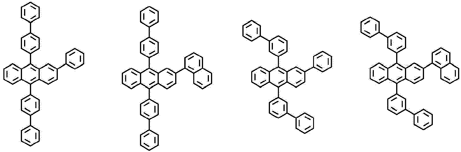


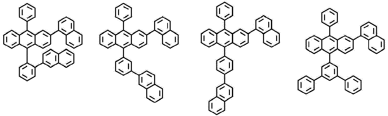


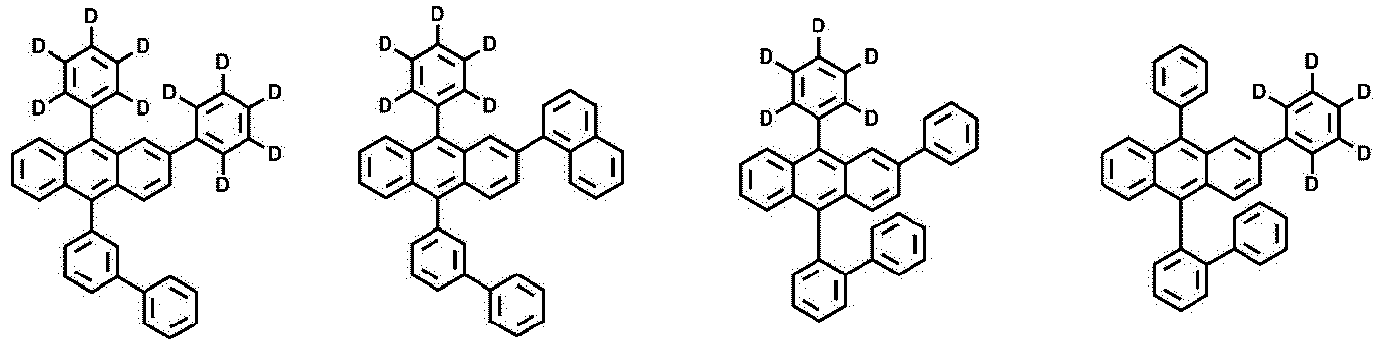


- In an exemplary embodiment of the present specification,
Formula 2 may be represented by the following Formula 2-1.
- In Formula 2-1,
definitions of Cy1 to Cy3, X1, Ra, and Rb are the same as those defined inFormula 2. - According to an exemplary embodiment of the present specification, Cy1 to Cy3 are the same as or different from each other, and are each independently a substituted or unsubstituted aromatic hydrocarbon ring having 6 to 60 carbon atoms; or a substituted or unsubstituted aromatic hetero ring having 2 to 60 carbon atoms, and Cy1 and Cy2 may be bonded to each other to form a substituted or unsubstituted ring.
- According to another exemplary embodiment, Cy1 to Cy3 are the same as or different from each other, and are each independently a substituted or unsubstituted aromatic hydrocarbon ring having 6 to 30 carbon atoms; or a substituted or unsubstituted aromatic hetero ring having 2 to 30 carbon atoms, and Cy1 and Cy2 may be bonded to each other to form a substituted or unsubstituted ring.
- According to an exemplary embodiment of the present specification, Ra is a substituted or unsubstituted alkyl group; a substituted or unsubstituted aryl group; or a substituted or unsubstituted heterocyclic group, or is bonded to Cy1 or Cy3 to form a substituted or unsubstituted ring.
- According to an exemplary embodiment of the present specification, Ra is a substituted or unsubstituted alkyl group having 1 to 60 carbon atoms; a substituted or unsubstituted aryl group having 6 to 60 carbon atoms; or a substituted or unsubstituted heterocyclic group having 2 to 60 carbon atoms, or is bonded to Cy1 or Cy3 to form a substituted or unsubstituted ring.
- According to an exemplary embodiment of the present specification, Ra is a substituted or unsubstituted alkyl group having 1 to 20 carbon atoms; a substituted or unsubstituted aryl group having 6 to 30 carbon atoms; or a substituted or unsubstituted heterocyclic group having 2 to 30 carbon atoms, or is bonded to Cy1 or Cy3 to form a substituted or unsubstituted ring.
- According to an exemplary embodiment of the present specification, Rb is a substituted or unsubstituted alkyl group; a substituted or unsubstituted aryl group; or a substituted or unsubstituted heterocyclic group, or is bonded to Cy1 or Cy3 to form a substituted or unsubstituted ring.
- According to an exemplary embodiment of the present specification, Rb is a substituted or unsubstituted alkyl group having 1 to 60 carbon atoms; a substituted or unsubstituted aryl group having 6 to 60 carbon atoms; or a substituted or unsubstituted heterocyclic group having 2 to 60 carbon atoms, or is bonded to Cy1 or Cy3 to form a substituted or unsubstituted ring.
- According to an exemplary embodiment of the present specification, Rb is a substituted or unsubstituted alkyl group having 1 to 20 carbon atoms; a substituted or unsubstituted aryl group having 6 to 30 carbon atoms; or a substituted or unsubstituted heterocyclic group having 2 to 30 carbon atoms, or is bonded to Cy1 or Cy3 to form a substituted or unsubstituted ring.
- According to an exemplary embodiment of the present specification, the compound represented by
Formula 2 may be any one of the following compounds, but is not limited thereto.


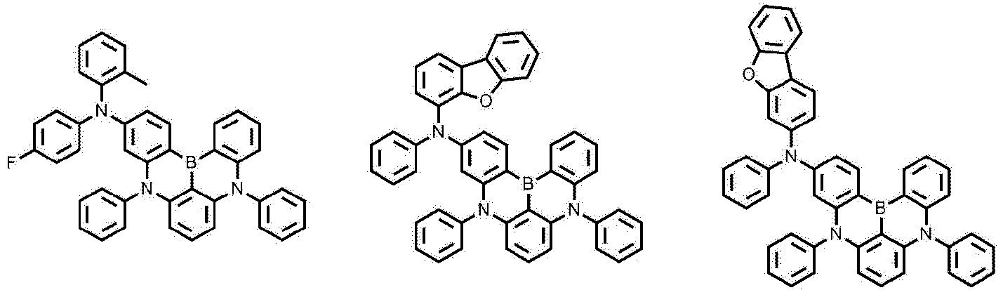


- In the compound represented by
Formula 1 according to an exemplary embodiment of the present invention, a core structure may be prepared as in the followingReaction Formula Formula 2 according to an exemplary embodiment of the present invention, a core structure may be prepared as in the followingReaction Formula 3. The substituents ofFormulae Reaction Formulae 1 to 3 may be bonded by methods known in the art, and the type or position of the substituent, or the number of substituents may be changed according to the technology known in the art.

- In
Reaction Formula 1, definitions of L1, L3, Ar1, Ar3, R1, R2, n1, and n2 are the same as those defined in the above-describedFormula 1.
- In
Reaction Formula 2, definitions of L1 to L3, Ar1 to Ar3, R1, R2, n1, and n2 are the same as those defined in the above-describedFormula 1.
- In
Reaction Formula 3, definitions of Cy1 to Cy3, Y1, Y2, and X1 are the same as those defined in the above-describedFormula 2. - In the present specification, compounds having various energy bandgaps may be synthesized by introducing various substituents into the core structures prepared in
Reaction Formulae 1 to 3. Further, in the present specification, various substituents may be introduced into the core structures prepared inReaction Formulae 1 to 3 to adjust the HOMO and LUMO energy levels of a compound. - The organic light emitting device of the present specification may be manufactured by typical manufacturing methods and materials of an organic light emitting device, except that a light emitting layer is formed using the above-described compounds represented by
Formulae - The compounds represented by
Formulae 1 to 2 may be formed as an organic material layer by not only a vacuum deposition method, but also a solution application when an organic light emitting device is manufactured. Here, the solution application method means spin coating, dip coating, inkjet printing, screen printing, a spray method, roll coating, and the like, but is not limited thereto. - The organic material layer of the organic light emitting device of the present specification may be composed of a single-layered structure, but may also be composed of a multi-layered structure in which two or more organic material layers are stacked. For example, the organic light emitting device of the present specification may have a structure including one or more layers of a hole transport layer, a hole injection layer, an electron blocking layer, an electron transport and injection layer, an electron transport layer, an electron injection layer, a hole blocking layer, and an hole transport and injection layer, as organic material layers. However, the structure of the organic light emitting device is not limited thereto, and may include a fewer or greater number of organic material layers.
- The organic light emitting device of the present specification includes an organic material layer including a light emitting layer, and the light emitting layer includes the compound represented by
Formula 1 and the compound represented byFormula 2. The compound represented byFormula 2 may be included in an amount of 1 part by weight to 20 parts by weight based on 100 parts by weight of the compound represented byFormula 1, and according to an example, may be included in an amount of 1 part by weight to 10 parts by weight based on 100 parts by weight of the compound represented byFormula 1. When the content of the compound represented byFormula 2 satisfies the above-range, there is an advantage in that the manufactured organic light emitting device has a low driving voltage, high light emitting efficiency, and a long service life. - According to an exemplary embodiment of the present specification, the light emitting layer of the organic light emitting device includes the compound represented by
Formula 1 as a host of the light emitting layer, and includes the compound represented byFormula 2 as a dopant of the light emitting layer. - In the organic light emitting device of the present invention, the organic material layer may include an electron blocking layer, and as the electron blocking layer, materials known in the art may be used.
- In an exemplary embodiment of the present specification, the first electrode is a positive electrode, and the second electrode is a negative electrode.
- According to another exemplary embodiment, the first electrode is a negative electrode, and the second electrode is a positive electrode.
- The organic light emitting device may have, for example, a stacking structure described below, but the stacking structure is not limited thereto.
- (1) Positive electrode/Hole transport layer/Light emitting layer/Negative electrode
- (2) Positive electrode/Hole injection layer/Hole transport layer/Light emitting layer/Negative electrode
- (3) Positive electrode/Hole transport layer/Light emitting layer/Electron transport layer/Negative electrode
- (4) Positive electrode/Hole transport layer/Light emitting layer/Electron transport layer/Electron injection layer/Negative electrode
- (5) Positive electrode/Hole injection layer/Hole transport layer/Light emitting layer/Electron transport layer/Negative electrode
- (6) Positive electrode/Hole injection layer/Hole transport layer/Light emitting layer/Electron transport layer/Electron injection layer/Negative electrode
- (7) Positive electrode/Hole transport layer/Electron blocking layer/Light emitting layer/Electron transport layer/Negative electrode
- (8) Positive electrode/ Hole transport layer/Electron blocking layer/Light emitting layer/Electron transport layer/Electron injection layer/Negative electrode
- (9) Positive electrode/Hole injection layer/Hole transport layer/Electron blocking layer/Light emitting layer/Electron transport layer/Negative electrode
- (10) Positive electrode/Hole injection layer/Hole transport layer/Electron blocking layer/Light emitting layer/Electron transport layer/Electron injection layer/Negative electrode
- (11) Positive electrode/Hole transport layer/Light emitting layer/Hole blocking layer/Electron transport layer/Negative electrode
- (12) Positive electrode/Hole transport layer/Light emitting layer/Hole blocking layer/Electron transport layer/Electron injection layer/Negative electrode
- (13) Positive electrode/Hole injection layer/Hole transport layer/Light emitting layer/Hole blocking layer/Electron transport layer/Negative electrode
- (14) Positive electrode/Hole injection layer/Hole transport layer/Light emitting layer/Hole blocking layer/Electron transport layer/Electron injection layer/Negative electrode
- (15) Positive electrode/Hole injection layer/First hole transport layer/Second hole transport layer/Light emitting layer/Electron transport layer/Electron injection layer/Negative electrode
- The structure of the organic light emitting device of the present invention may have structures illustrated in
FIGS. 1 and2 , but is not limited thereto. -
FIG. 1 exemplifies a structure of an organic light emitting device in which apositive electrode 2, alight emitting layer 3, and anegative electrode 4 are sequentially stacked on asubstrate 1. -
FIG. 2 exemplifies a structure of an organic light emitting device in which apositive electrode 2, ahole injection layer 5, a firsthole transport layer 6, a secondhole transport layer 7, alight emitting layer 8, anelectron transport layer 9, anelectron injection layer 10, and anegative electrode 4 are sequentially stacked on asubstrate 1. - For example, the organic light emitting device according to the present invention may be manufactured by depositing a metal or a metal oxide having conductivity, or an alloy thereof on a substrate to form a positive electrode, forming an organic material layer including a hole injection layer, a hole transport layer, a light emitting layer, an electron blocking layer, an electron transport layer, and an electron injection layer thereon, and then depositing a material, which may be used as a negative electrode, thereon, by using a physical vapor deposition (PVD) method such as sputtering or e-beam evaporation. In addition to the method described above, an organic light emitting device may also be made by sequentially depositing a negative electrode material, an organic material layer, and a positive electrode material on a substrate.
- The organic material layer may further include one or more layers of a hole transport layer, a hole injection layer, an electron blocking layer, an electron transport and injection layer, an electron transport layer, an electron injection layer, a hole blocking layer, and a hole transport and injection layer.
- The organic material layer may have a multi-layered structure including a hole injection layer, a hole transport layer, a hole transport and injection layer, an electron blocking layer, a light emitting layer, an electron transport layer, an electron injection layer, an electron transport and injection layer, and the like, but is not limited thereto, and may also have a single-layered structure. Further, the organic material layer may be manufactured to include a fewer number of layers by a method such as a solvent process, for example, spin coating, dip coating, doctor blading, screen printing, inkjet printing, or a thermal transfer method, using various polymer materials, instead of a deposition method.
- The positive electrode is an electrode which injects holes, and as a positive electrode material, materials having a high work function are usually preferred so as to facilitate the injection of holes into an organic material layer. Specific examples of the positive electrode material which may be used in the present invention include: a metal, such as vanadium, chromium, copper, zinc, and gold, or an alloy thereof; a metal oxide, such as zinc oxide, indium oxide, indium tin oxide (ITO), and indium zinc oxide (IZO); a combination of a metal and an oxide, such as ZnO : Al or SnO2 : Sb; a conductive polymer, such as poly(3-methylthiophene), poly[3,4-(ethylene-1,2-dioxy)thiophene] (PEDOT), polypyrrole, and polyaniline; and the like, but are not limited thereto.
- The negative electrode is an electrode which injects electrons, and as a negative electrode material, materials having a low work function are usually preferred so as to facilitate the injection of electrons into an organic material layer. Specific examples of the negative electrode material include: a metal such as magnesium, calcium, sodium, potassium, titanium, indium, yttrium, lithium, gadolinium, aluminum, silver, tin, and lead, or an alloy thereof; a multi-layer structured material, such as LiF/Al or LiO2/Al; and the like, but are not limited thereto.
- The hole injection layer is a layer which serves to facilitate the injection of holes from a positive electrode to a light emitting layer, and a hole injection material is preferably a material which may proficiently accept holes from a positive electrode at a low voltage, and the highest occupied molecular orbital (HOMO) of the hole injection material is preferably a value between the work function of the positive electrode material and the HOMO of the peripheral organic material layer. Specific examples of the hole injection material include metal porphyrin, oligothiophene, arylamine-based organic materials, hexanitrile hexaazatriphenylene-based organic materials, quinacridone-based organic materials, perylene-based organic materials, anthraquinone, polyaniline-based and polythiophene-based conductive polymers, and the like, but are not limited thereto. The hole injection layer may have a thickness of 1 nm to 150 nm. When the hole injection layer has a thickness of 1 nm or more, there is an advantage in that it is possible to prevent hole injection characteristics from deteriorating, and when the hole injection layer has a thickness of 150 nm or less, there is an advantage in that it is possible to prevent the driving voltage from being increased in order to improve the movement of holes due to the too thick hole injection layer.
- The hole transport layer may serve to smoothly transport holes. A hole transport material is suitably a material having high hole mobility which may accept holes from a positive electrode or a hole injection layer and transfer the holes to a light emitting layer. Specific examples thereof include arylamine-based organic materials, conductive polymers, block copolymers having both conjugated portions and non-conjugated portions, and the like, but are not limited thereto.
- The organic light emitting device may include an electron blocking layer provided between the hole transport layer and the light emitting layer. As the electron blocking layer, the above-described compound or a material known in the art may be used.
- When the organic light emitting device includes an additional light emitting layer in addition to the light emitting layer including the above-described compounds represented by
Formulae - Examples of a host material for the additional light emitting layer include fused aromatic ring derivatives, or hetero ring-containing compounds, and the like. Specifically, examples of the fused aromatic ring derivative include anthracene derivatives, pyrene derivatives, naphthalene derivatives, pentacene derivatives, phenanthrene compounds, fluoranthene compounds, and the like, and examples of the hetero ring-containing compound include carbazole derivatives, dibenzofuran derivatives, ladder-type furan compounds, pyrimidine derivatives, and the like, but the examples thereof are not limited thereto.
- When the additional light emitting layer emits red light, it is possible to use a phosphorescent material such as bis(1-phenylisoquinoline)acetylacetonate iridium (PIQIr(acac)), bis(1-phenylquinoline)acetylacetonate iridium (PQIr(acac)), tris(1-phenylquinoline)iridium (PQIr), or octaethylporphyrin platinum (PtOEP), or a fluorescent material such as tris(8-hydroxyquinolino)aluminum (Alq3) as a light emitting dopant, but the light emitting dopant is not limited thereto. When the additional light emitting layer emits green light, it is possible to use a phosphorescent material such as fac tris(2-phenylpyridine)iridium (Ir(ppy)3), or a fluorescent material such as tris(8-hydroxyquinolino)aluminum (Alq3), as the light emitting dopant, but the light emitting dopant is not limited thereto. When the additional light emitting layer emits blue light, it is possible to use a phosphorescent material such as (4,6-F2ppy)2Irpic, or a fluorescent material such as spiro-DPVBi, spiro-6P, distyryl benzene (DSB), distyryl arylene (DSA), a PFO-based polymer or a PPV-based polymer as the light emitting dopant, but the light emitting dopant is not limited thereto.
- The electron transport layer may serve to smoothly transport electrons. An electron transport material is suitably a material having high electron mobility which may proficiently accept electrons from a negative electrode and transfer the electrons to a light emitting layer. Specific examples thereof include: Al complexes of 8-hydroxyquinoline; complexes including Alq3; organic radical compounds; hydroxyflavone-metal complexes; and the like, but are not limited thereto. The electron transport layer may have a thickness of 1 nm to 50 nm. When the electron transport layer has a thickness of 1 nm or more, there is an advantage in that it is possible to prevent electron transport characteristics from deteriorating, and when the electron transport layer has a thickness of 50 nm or less, there is an advantage in that it is possible to prevent the driving voltage from being increased in order to improve the movement of electrons due to the too thick electron transport layer.
- The electron injection layer may serve to smoothly inject electrons. An electron injection material is preferably a compound which has a capability of transporting electrons, an effect of injecting electrons from a negative electrode, and an excellent effect of injecting electrons into a light emitting layer or a light emitting material, prevents excitons produced from a light emitting layer from moving to a hole injection layer, and is also excellent in the ability to form a thin film. Specific examples thereof include fluorenone, anthraquinodimethane, diphenoquinone, thiopyran dioxide, oxazole, oxadiazole, triazole, imidazole, perylenetetracarboxylic acid, fluorenylidene methane, anthrone, and the like, and derivatives thereof, metal complex compounds, nitrogen-containing 5-membered ring derivatives, and the like, but are not limited thereto.
- Examples of the metal complex compounds include 8-hydroxyquinolinato lithium, bis(8-hydroxyquinolinato) zinc, bis(8-hydroxyquinolinato) copper, bis(8-hydroxyquinolinato) manganese, tris(8-hydroxyquinolinato) aluminum, tris(2-methyl-8-hydroxyquinolinato) aluminum, tris(8-hydroxyquinolinato) gallium, bis(10-hydroxybenzo[h]quinolinato) beryllium, bis(10-hydroxybenzo[h]quinolinato) zinc, bis(2-methyl-8-quinolinato) chlorogallium, bis(2-methyl-8-quinolinato)(o-cresolato) gallium, bis(2-methyl-8-quinolinato)(1-naphtholato) aluminum, bis(2-methyl-8-quinolinato)(2-naphtholato) gallium, and the like, but are not limited thereto.
- The hole blocking layer is a layer which blocks holes from reaching a negative electrode, and may be generally formed under the same conditions as those of the hole injection layer. Specific examples thereof include oxadiazole derivatives or triazole derivatives, phenanthroline derivatives, BCP, aluminum complexes, and the like, but are not limited thereto.
- The organic light emitting device according to the present invention may be a top emission type, a bottom emission type, or a dual emission type according to the material to be used.
- Hereinafter, the present specification will be described in detail with reference to Examples for specifically describing the present specification. However, the Examples according to the present specification may be modified in various forms, and it is not interpreted that the scope of the present application is limited to the Examples described in detail below. The Examples of the present application are provided to more completely explain the present specification to a person with ordinary skill in the art.
- The compound according to an exemplary embodiment of the present specification may be prepared by a preparation method to be described below.
- For example, the core structure of the compound having the structure of
Formula 1 may be prepared byReaction Formulae 1 to 3. The substituents may be bonded by a method known in the art, and the type or position of the substituent or the number of substituents may be changed according to the technology known in the art. -

- Bromobenzene (27.3 g, 174 mmol) was dissolved in THF (140 ml) dried under a nitrogen atmosphere, t-BuLi (140 ml, a 1.7 M pentane solution) was slowly added thereto at -78°C, and then the resulting solution was stirred at the same temperature for 1 hour. Here, after 2-bromoanthraquinone (20 g, 70 mmol) was added thereto, the resulting solution was warmed to room temperature and stirred for 3 hours. After an aqueous ammonium chloride solution was added to the reaction solution, an extraction with chloroform was performed. The organic layer was dried over anhydrous magnesium sulfate, and the solvent was removed. The obtained mixture was recrystallized with a small amount of diethyl ether to obtain Compound 1-a (25.2 g, yield 82%).
- After Compound 1-a (25.2 g, 57 mmol) was dispersed in acetic acid (380 ml) under a nitrogen atmosphere, KI (94.4 g, 568 mmol) and NaPO2H2 (100 g, 1136 mmol) were added thereto, and then the resulting solution was stirred under reflux for 3 hours. The solution was cooled at room temperature and then filtered, and washed with water and ethanol, and then dried under vacuum to obtain Compound 1-b (19.2 g, yield 82.5%). As a result of mass spectrum measurement, a peak was confirmed at [M+H+]=409.
- After Compound 1-b (19.2 g, 47 mmol), bis(pinacolato)diboron (14.3 g, 56 mmol), potassium acetate (13.8 g, 141 mmol), and palladium(diphenylphosphitoferocene)chloride (1.24 g, 1.7 mmol) were mixed with dioxane (160 ml), the resulting mixture was refluxed for 6 hours. After the reaction solution was cooled, dioxane was removed under reduced pressure, and then the residue was dissolved in chloroform, water was added thereto, and an extraction was performed. (Performed three times) The organic layer was separated and dried over anhydrous magnesium sulfate, and the solvent was removed under reduced pressure. In this case, the obtained material was purified using column chromatography to obtain Compound 1-c (15.2 g, yield 71%). As a result of mass spectrum measurement, a peak was confirmed at [M+H+]=457.
- After Compound 1-c (15.2 g, 33 mmol) and bromobenzene (5.2 g, 33.3 mmol) were dissolved in THF (100 ml), Pd(PPh3)4 (1.54 g, 1.3 mmol) and 30 ml of an aqueous 2M K2CO3 solution were added thereto, and the resulting solution was refluxed for 24 hours. The reaction solution was cooled, and the organic layer was extracted with ethyl acetate, and then dried over anhydrous magnesium sulfate. The organic solvent was removed under reduced pressure, and the residue was purified using column chromatography to obtain Compound A (10 g, yield 73.8%). As a result of mass spectrum measurement, a peak was confirmed at [M+H+]=407.
-

- Compound B was obtained by performing synthesis and purification in the same manner as in Synthesis Example 1-d, except that bromobenzene was changed into 1-bromonaphthalene. As a result of mass spectrum measurement, a peak was confirmed at [M+H+]=457.
-

- Compound C was obtained by performing synthesis and purification in the same manner as in Synthesis Example 1-d, except that bromobenzene was changed into 9-bromophenanthrene. As a result of mass spectrum measurement, a peak was confirmed at [M+H+]=507.
-

- Compound D was obtained by performing synthesis and purification in the same manner as in Synthesis Example 1-d, except that bromobenzene was changed into 1-bromo-6-phenylnaphthalene. As a result of mass spectrum measurement, a peak was confirmed at [M+H+]=533.
-

- Compound E was obtained by performing synthesis and purification in the same manner as in Synthesis Example 1-d, except that bromobenzene was changed into 1-bromo-7-phenylnaphthalene. As a result of mass spectrum measurement, a peak was confirmed at [M+H+]=533.
-

- Compound F was obtained by performing synthesis and purification in the same manner as in Synthesis Example 1-d, except that bromobenzene was changed into 1-bromodibenzofuran. As a result of mass spectrum measurement, a peak was confirmed at [M+H+]=497.
-

- Compound G was obtained by performing synthesis and purification in the same manner as in Synthesis Example 1-d, except that bromobenzene was changed into 2-bromodibenzofuran. As a result of mass spectrum measurement, a peak was confirmed at [M+H+]=497.
-
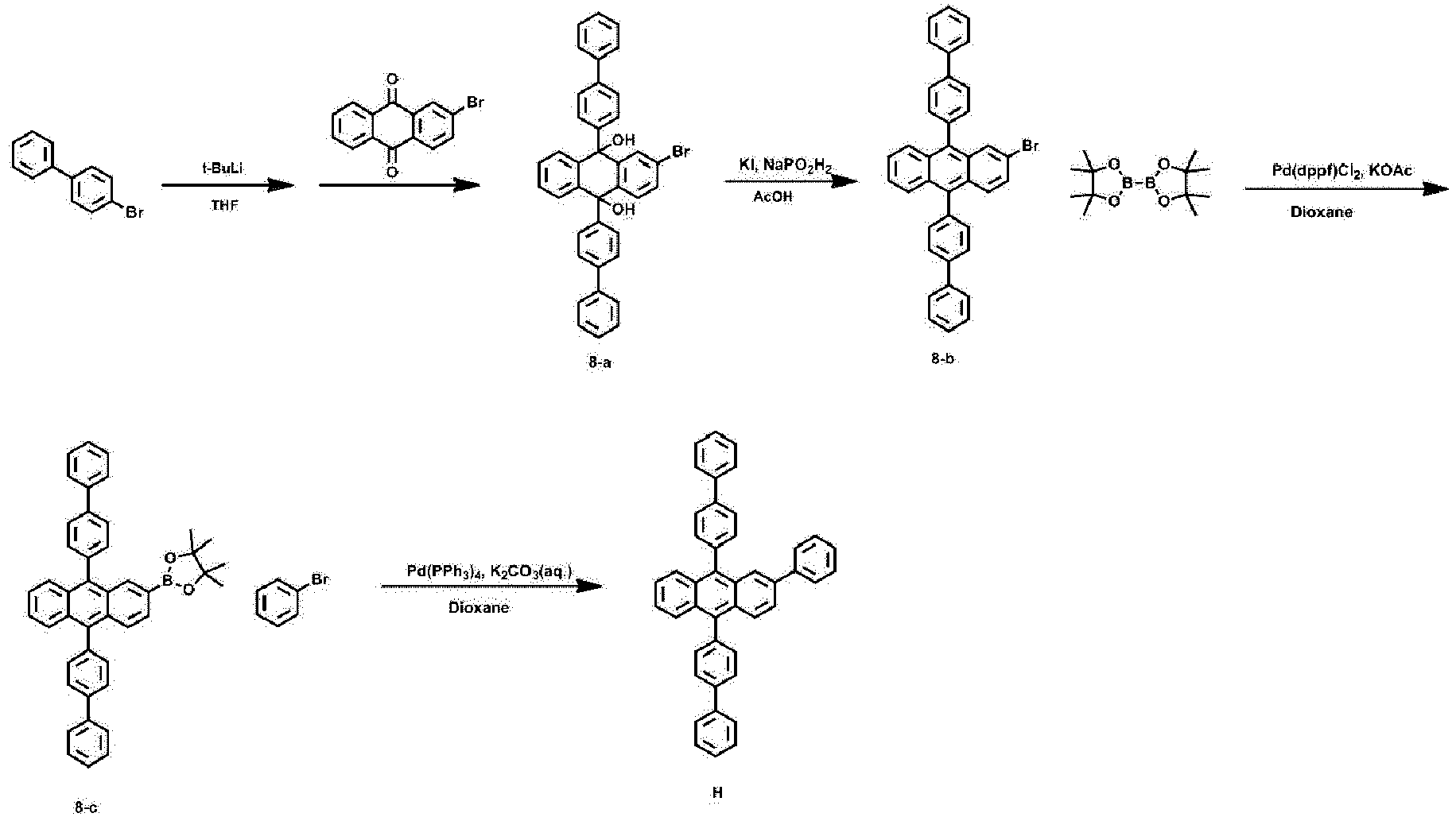
- Compound 8-a was obtained by performing synthesis and purification in the same manner as in Synthesis Example 1-a, except that bromobenzene was changed into 4-bromo-1,1'-biphenyl.
- Compound 8-b was obtained by performing synthesis and purification in the same manner as in Synthesis Example 1-b, except that Compound 1-a was changed into Compound 8-a.
- Compound 8-c was obtained by performing synthesis and purification in the same manner as in Synthesis Example 1-c, except that Compound 1-b was changed into Compound 8-b.
- Compound H was obtained by performing synthesis and purification in the same manner as in Synthesis Example 1-d, except that Compound 1-c was changed into Compound 8-c. As a result of mass spectrum measurement, a peak was confirmed at [M+H+]=559.
-

- Compound I was obtained by performing synthesis and purification in the same manner as in Synthesis Example 8-d, except that bromobenzene was changed into 1-bromonaphthalene. As a result of mass spectrum measurement, a peak was confirmed at [M+H+]=609.
-

- Compound 10-a was obtained by performing synthesis and purification in the same manner as in Synthesis Example 1-a, except that bromobenzene was changed into 3-bromo-1,1'-biphenyl.
- Compound 10-b was obtained by performing synthesis and purification in the same manner as in Synthesis Example 1-b, except that Compound 1-a was changed into Compound 10-a.
- Compound 10-c was obtained by performing synthesis and purification in the same manner as in Synthesis Example 1-c, except that Compound 1-b was changed into Compound 10-b.
- Compound J was obtained by performing synthesis and purification in the same manner as in Synthesis Example 1-d, except that Compound 1-c was changed into Compound 10-c. As a result of mass spectrum measurement, a peak was confirmed at [M+H+]=609.
-

- 2-bromoanthracene (50 g, 194 mmol) and 1-naphthylboronic acid (33.4 g, 194 mmol) were dissolved in THF (600 ml), and then Pd(PPh3)4 (8.98 g, 7.8 mmol) and 120 ml of an aqueous 2M K2CO3 solution were added thereto, and the resulting solution was refluxed for 24 hours. The reaction solution was cooled, and the organic layer was extracted with ethyl acetate, and then dried over anhydrous magnesium sulfate. The organic solvent was removed under reduced pressure, and the residue was purified using column chromatography to obtain Compound 11-a (51 g, 86.1%).
- After Compound 11-a (51 g, 168 mmol) was dispersed in 400 ml of dimethylformamide, a solution of n-bromosuccinimide (29.8g, 168mmol) dissolved in 50 ml of dimethylformamide was slowly added dropwise thereto. After reaction at room temperature for 2 hours, 1 L of water was added dropwise thereto. When a solid was produced, the solid was filtered, and then dissolved in ethyl acetate, and the resulting solution was put into a separatory funnel, and then washed several times with distilled water. The solution was recrystallized in EA to obtain Compound 11-b (45g, 70%).
- Compound 11-b (45 g, 117 mmol) and phenylboronic acid (14.3 g, 117 mmol) were dissolved in 400 ml of THF, and then Pd(PPh3)4 (5.4 g, 4.7 mmol) and 100 ml of an aqueous 2M K2CO3 solution were added thereto, and the resulting solution was stirred under reflux for 24 hours. The reaction solution was cooled and the produced solid was filtered. The solid was dissolved in ethyl acetate, and then recrystallized to obtain Compound 11-c (38 g, 85%).
- After Compound 11-c (38 g, 100 mmol) was dispersed in 500 ml of dimethylformamide, a solution of n-bromosuccinimide (17.8 g, 100 mmol) dissolved in 50 ml of dimethylformamide was slowly added dropwise thereto. After reaction at room temperature for 2 hours, 1 L of water was added dropwise thereto. When a solid was produced, the solid was filtered, and then dissolved in ethyl acetate, and the resulting solution was put into a separatory funnel, and then washed several times with distilled water. The solution was recrystallized in EA to obtain Compound 11-d (35 g, 76%).
- Compound 11-b (35 g, 76 mmol) and 1-naphthylboronic acid (15.1 g, 76 mmol) were dissolved in 250 ml of THF, and then Pd(PPh3)4 (3.5 g, 3 mmol) and 50 ml of an aqueous 2M K2CO3 solution were added thereto, and the resulting solution was stirred under reflux for 24 hours. The reaction solution was cooled and the produced solid was filtered. The residue was purified with column chromatography to obtain Compound K (31 g, 76%). As a result of mass spectrum measurement, a peak was confirmed at [M+H+]=533.
-

- Compound 12-a was obtained by performing synthesis and purification in the same manner as in Synthesis Example 11-c, except that phenylboronic acid was changed into 4-bromo-1,1'-biphenylboronic acid.
- Compound 12-b was obtained by performing synthesis and purification in the same manner as in Synthesis Example 11-d, except that Compound 11-c was changed into Compound 12-a.
- Compound L was obtained by performing synthesis and purification in the same manner as in Synthesis Example 11-e, except that Compound 11-d was changed into Compound 12-b. As a result of mass spectrum measurement, a peak was confirmed at [M+H+]=609.
-

- The synthesized Compound A (20g) and AlCl3(4 g) were put into C6D6 (400 ml), and the resulting solution was stirred for 2 hours. After the reaction was completed, D2O (60 ml) was added thereto, the resulting solution was stirred for 30 minutes, and then trimethylamine (6 ml) was added dropwise thereto. The reaction solution was transferred to a separatory funnel, and an extraction with water and toluene was performed. The extract was dried over MgSO4, and then the residue was recrystallized with ethyl acetate to obtain Compound M at a yield of 60%. As a result of mass spectrum measurement, a peak was confirmed at [M+H+]=429.
-

- Compound N was obtained by performing synthesis and purification in the same manner as in Synthesis Example 13, except that Compound A was changed into Compound B. As a result of mass spectrum measurement, a peak was confirmed at [M+H+]=480.
-

- A flask containing 1,2,3-tribromo-5-chlorobenzene (5 g), bis-(4-(tert-butyl)phenyl)amine (8 g), Pd(PtBu3)2 (0.15 g), NaOtBu (4.1 g), and xylene (50 ml) was heated at 130°C, and the resulting solution was stirred for 3 hours. The reaction solution was cooled to room temperature, the liquid was aliquoted by adding water and ethyl acetate thereto, and then the solvent was distilled off under reduced pressure. The resulting product was purified with recrystallization (ethyl acetate/hexane) to obtain Compound 15-a (7.5 g).
- An n-butyllithium pentane solution (8 ml, 2.5 M in hexane) was added to a flask containing Compound 15-a (7.5 g) and xylene (100 ml) at 0°C under an argon atmosphere. After the completion of dropwise addition, the resulting solution was warmed to 50°C and stirred for 2 hours. The resulting solution was cooled to -40°C, boron tribromide (2.88 ml) was added thereto, and the resulting solution was stirred for 4 hours while being warmed to room temperature. Thereafter, the resulting solution was cooled again to 0°C, N,N-diisopropylethylamine (8 ml) was added thereto, and the reaction solution was further stirred at room temperature for 30 minutes. After the liquid was aliquoted by adding sat. aq. NaCl and ethyl acetate thereto, the solvent was distilled off under reduced pressure. The resulting product was purified with a silica gel column chromatography (eluent: hexane/ethyl acetate = 1/30) to obtain Compound 15-b (1.6 g).
- A flask containing Compound 15-b (1.6 g), diphenylamine (0.44 g), Pd(PtBu3)2 (24 mg), CsCO3 (2.3 g), and xylene (20 ml) was heated at 130°C, and the resulting solution was stirred for 2 hours. The reaction solution was cooled to room temperature, the liquid was aliquoted by adding sat. aq. NH4Cl and toluene thereto, and then the solvent was distilled off under reduced pressure. The resulting product was purified with a silica gel column chromatography (eluent: hexane/ethyl acetate = 1/30) to obtain Compound BD-A (1.3 g). As a result of mass spectrum measurement, a peak was confirmed at [M+H+]=812.
-

- Compound 16-a was obtained by performing synthesis and purification in the same manner as in Synthesis Example 15-a, except that 1,2,3-tribromo-5-methylbenzene was used instead of 1,2,3-tribromo-5-chlorobenzene, and di-p-tolylamine was used instead of bis-(4-(tert-butyl)phenyl)amine.
- Compound BD-B was obtained by performing synthesis and purification in the same manner as in Synthesis Example 15-b, except that Compound 16-a was used instead of Compound 15-a. As a result of mass spectrum measurement, a peak was confirmed at [M+H+]=491.
- The structures of the compounds used in the following Examples and Comparative Examples are as follows, and among the structures, the compounds corresponding to
Formulae 1 to 2 of the present application were prepared by the procedures in the above-describedReaction Formulae 1 to 3.


- A glass substrate thinly coated with indium tin oxide (ITO) to have a thickness of 150 nm was put into distilled water in which a detergent was dissolved, and ultrasonically washed. In this case, a product manufactured by the Fischer Co., was used as the detergent, and distilled water twice filtered using a filter manufactured by Millipore Co., was used as the distilled water. After the ITO was washed for 30 minutes, ultrasonic washing was repeated twice by using distilled water for 10 minutes. After the washing using distilled water was completed, ultrasonic washing was conducted by using isopropyl alcohol, acetone, and methanol solvents, and the resulting product was dried and then transported to a plasma washing machine. Furthermore, the substrate was washed using nitrogen plasma for 5 minutes, and then was transported to a vacuum deposition machine. The following HAT-CN compound was thermally vacuum-deposited to have a thickness of 5 nm on the ITO transparent electrode thus prepared, thereby forming a hole injection layer. Subsequently, HTL1 was thermally vacuum-deposited to have a thickness of 100 nm, and then HTL2 was thermally vacuum-deposited to have a thickness of 10 nm, thereby forming a hole transport layer. Subsequently, Compound A as a host and BD-A as a dopant (weight ratio 95:5) were simultaneously vacuum-deposited, thereby forming a light emitting layer having a thickness of 20 nm. Subsequently, ETL was vacuum-deposited to have a thickness of 20 nm, thereby forming an electron transport layer. Subsequently, LiF was vacuum-deposited to have a thickness of 0.5 nm, thereby forming an electron injection layer. Subsequently, aluminum was deposited to have a thickness of 100 nm to form a negative electrode, thereby manufacturing an organic light emitting device.
- Each of organic light emitting devices was manufactured by the same method as Example 1 and by using the materials as a host and a dopant at the content (parts by weight based on 1 which is the sum of the contents of the host and the dopant) in the following Table 1. For each of the organic light emitting devices manufactured in Examples 1 to 17 and Comparative Examples 1 to 9, the driving voltage and light emitting efficiency were measured at a current density of 10 mA/cm2, and the time (LT) taken for the brightness to reach 97% as compared to the initial brightness was measured at a current density of 20 mA/cm2, and the results thereof are shown in the following Table 2.
[Table 1] Host Dopant Material Content Material Content Example 1 A 0.950 BD-A 0.05 Example 2 B 0.950 BD-A 0.05 Example 3 C 0.950 BD-A 0.05 Example 4 D 0.950 BD-A 0.05 Example 5 E 0.950 BD-A 0.05 Example 6 F 0.950 BD-A 0.05 Example 7 G 0.950 BD-A 0.05 Example 8 H 0.950 BD-A 0.05 Example 9 I 0.950 BD-A 0.05 Example 10 J 0.950 BD-A 0.05 Example 11 K 0.950 BD-A 0.05 Example 12 L 0.950 BD-A 0.05 Example 13 M 0.950 BD-A 0.05 Example 14 N 0.950 BD-A 0.05 Example 15 A 0.950 BD-8 0.05 Example 16 B 0.950 BD-B 0.05 Example 17 C 0.950 BD-B 0.05 Comparative Example 1 BH-A 0.950 BD-A 0.05 Comparative Example 2 BH-B 0.950 BD-A 0.05 Comparative Example 3 BH-C 0.950 BD-A 0.05 Comparative Example 4 BH-D 0.950 BD-A 0.05 Comparative Example 5 BH-E 0.950 BD-A 0.05 Comparative Example 6 BH-F 0.950 BD-A 0.05 Comparative Example 7 A 0.950 BD-C 0.05 Comparative Example 8 B 0.950 BD-C 0.05 Comparative Example 9 C 0.950 BD-C 0.05 [Table 2] 10 mA/cm2 measurement value LT (T97%, hr) (@20 mA/cm2) Driving voltage (V) Light emitting efficiency (Cd/A) Example 1 4.56 6.90 132 Example 2 4.68 6.92 149 Example 3 4.51 6.85 143 Example 4 4.43 7.01 142 Example 5 4.53 7.12 132 Example 6 4.61 6.95 140 Example 7 4.63 6.81 139 Example 8 4.71 6.71 138 Example 9 4.52 6.65 133 Example 10 4.61 6.82 141 Example 11 4.63 6.81 139 Example 12 4.71 6.71 138 Example 13 4.52 6.65 202 Example 14 4.61 6.82 210 Example 15 4.76 6.72 138 Example 16 4.50 6.96 140 Example 17 4.73 6.88 142 Comparative Example 1 4.82 6.12 52 Comparative Example 2 4.63 6.50 62 Comparative Example 3 4.79 6.68 40 Comparative Example 4 4.89 6.25 55 Comparative Example 5 4.82 4.20 71 Comparative Example 6 4.63 4.68 80 Comparative Example 7 4.79 4.52 84 Comparative Example 8 4.89 4.12 89 Comparative Example 9 4.91 4.12 75 - From Table 2, it can be confirmed that the organic light emitting devices of Examples 1 to 17, in which Ar1 and Ar2 of
Formula 1 have a substituted or unsubstituted phenyl group; or a substituted or unsubstituted biphenyl group have better device characteristics than the organic light emitting devices of Comparative Examples 1 to 6 which do not include the compound represented byFormula 1 according to the present application, and the organic light emitting devices of Comparative Examples 7 and 9, which do not include the compound represented byFormula 2 according to the present application. - In particular, it can be confirmed that in the case of Comparative Examples 1 to 3 in which a naphthyl group is substituted with any one of Ar1 and Ar2, Comparative Example 5 in which hydrogen is substituted with Ar3, and Comparative Example 6 in which a naphthobenzofuranyl group is substituted with Ar3, the time (LT) taken for the brightness to reach 97% as compared to the initial brightness at a current density of 20 mA/cm2, which indicates the service life of the organic light emitting device, is remarkably shorter than those of the organic light emitting devices of Examples 1 to 17
satisfying Formula 1 according to the present invention.
Claims (10)
- An organic light emitting device comprising:a first electrode;a second electrode provided to face the first electrode; andan organic material layer comprising a light emitting layer provided between the first electrode and the second electrode,wherein the light emitting layer comprises a compound represented by the following Formula 1 and a compound represented by the following Formula 2:
 Ar1 and Ar2 are the same as or different from each other, and are each independently a substituted or unsubstituted phenyl group; or a substituted or unsubstituted biphenyl group,Ar3 is a substituted or unsubstituted aryl group; a substituted or unsubstituted dibenzofuranyl group; or a substituted or unsubstituted dibenzothiophenyl group,L1 to L3 are the same as or different from each other, and are each independently a direct bond; or a substituted or unsubstituted arylene group,R1 and R2 are the same as or different from each other, and are each independently hydrogen; deuterium; a nitrile group; a halogen group; a substituted or unsubstituted silyl group; a substituted or unsubstituted boron group; a substituted or unsubstituted alkyl group; a substituted or unsubstituted alkenyl group; a substituted or unsubstituted alkynyl group; a substituted or unsubstituted alkoxy group; a substituted or unsubstituted aryloxy group; a substituted or unsubstituted cycloalkyl group; a substituted or unsubstituted amine group; a substituted or unsubstituted aryl group; or a substituted or unsubstituted heterocyclic group, andn1 is an integer form 0 to 4, and when n1 is 2 or higher, two or more R1's are the same as or different from each other,n2 is an integer from 0 to 3, and two or more R2's are the same as or different from each other provided that n2 is 2 or higher,
 X1 is B or P(=O),Y1 is O, S, or NRa,Y2 is O, S, or NRb,Cy1 to Cy3 are the same as or different from each other, and are each independently a substituted or unsubstituted aromatic hydrocarbon ring; or a substituted or unsubstituted aromatic hetero ring, and Cy1 and Cy2 are optionally bonded to each other to form a substituted or unsubstituted ring,Ra is a substituted or unsubstituted alkyl group; a substituted or unsubstituted aryl group; or a substituted or unsubstituted heterocyclic group, or is bonded to Cy1 or Cy3 to form a substituted or unsubstituted ring, andRb is a substituted or unsubstituted alkyl group; a substituted or unsubstituted aryl group; or a substituted or unsubstituted heterocyclic group, or is bonded to Cy2 or Cy3 to form a substituted or unsubstituted ring.
 - The organic light emitting device of claim 1,
wherein Ar1 and Ar2 are the same as or different from each other, and are each independently a phenyl group which is unsubstituted or substituted with deuterium or an aryl group having 6 to 60 carbon atoms; or a biphenyl group which is unsubstituted or substituted with deuterium or an aryl group having 6 to 60 carbon atoms. - The organic light emitting device of claim 1,
wherein Ar3 is a substituted or unsubstituted aryl group having 6 to 60 carbon atoms; a substituted or unsubstituted dibenzofuranyl group; or a substituted or unsubstituted dibenzothiophenyl group. - The organic light emitting device of claim 1,
wherein the compound represented by Formula 1 is represented by the following Formula 1-1 or 1-2: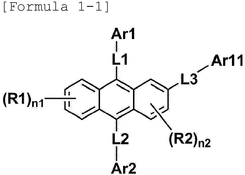

 definitions of L1 to L3, Ar1, Ar2, R1, R2, n1, and n2 are the same as those defined in Formula 1,Ar11 is a substituted or unsubstituted aryl group, andW is O or S.
 - The organic light emitting device of claim 1,
wherein the compound represented by Formula 1 is any one of the following compounds:


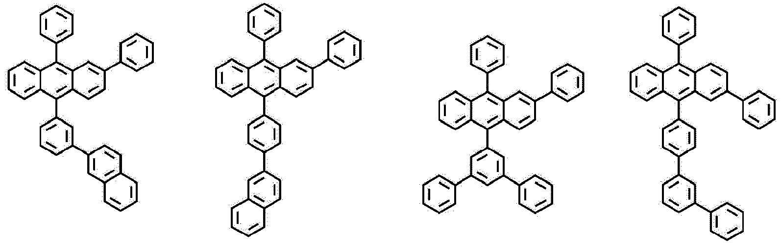


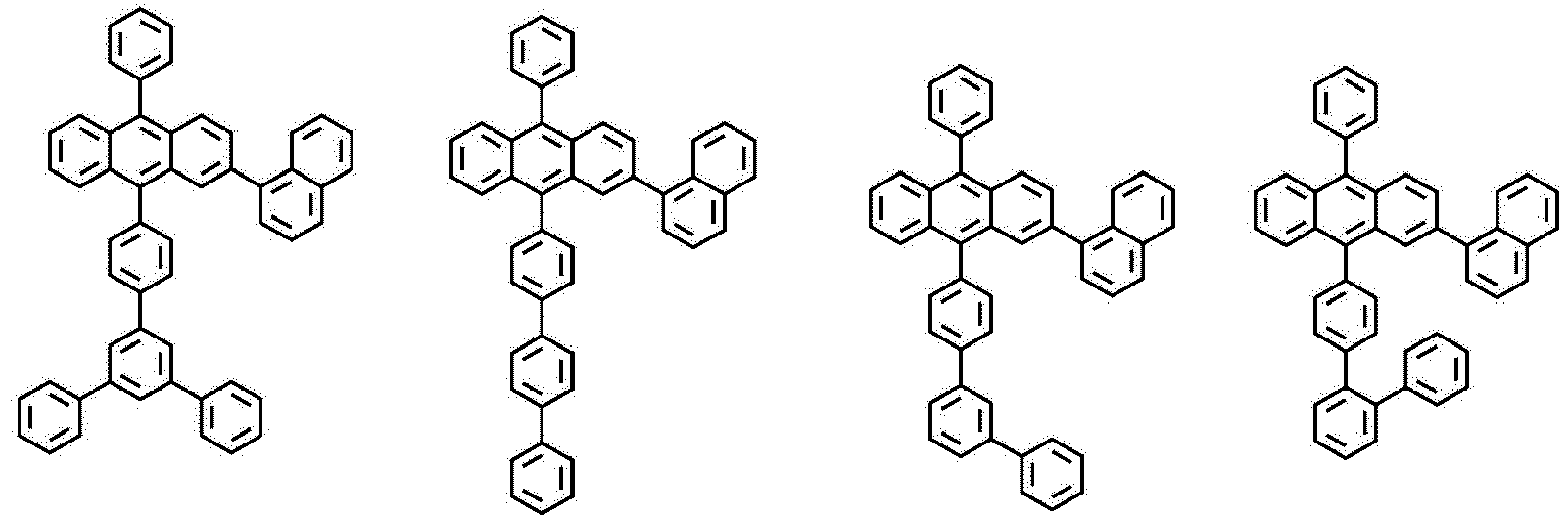


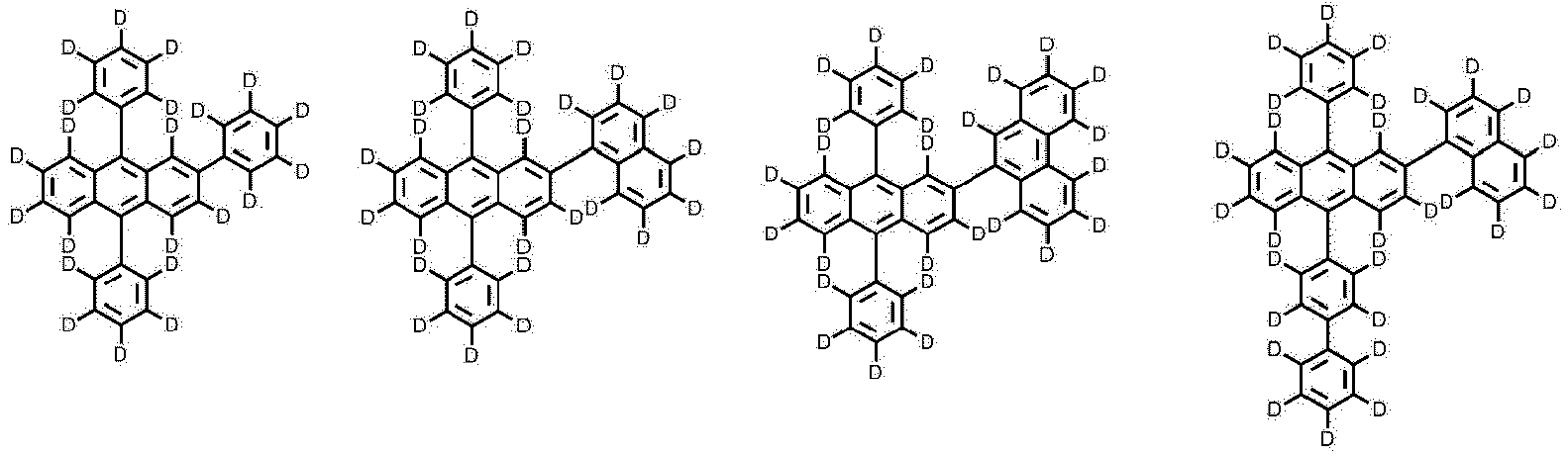
- The organic light emitting device of claim 1, wherein the compound represented by Formula 2 is represented by the following Formula 2-1:

definitions of Cy1 to Cy3, X1, Ra, and Rb are the same as those defined in Formula 2. - The organic light emitting device of claim 1,
wherein the compound represented by Formula 2 is any one of the following compounds:
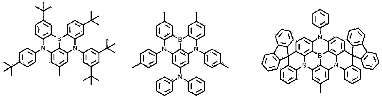


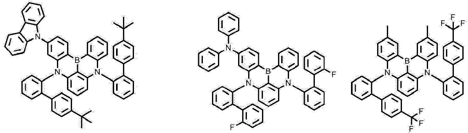
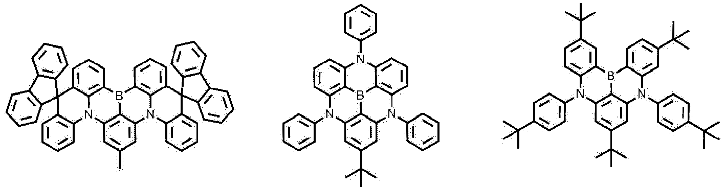
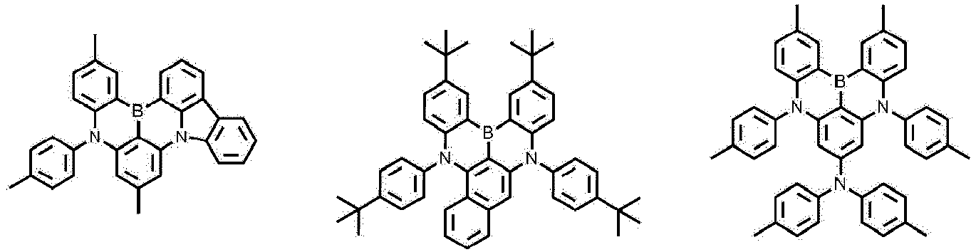


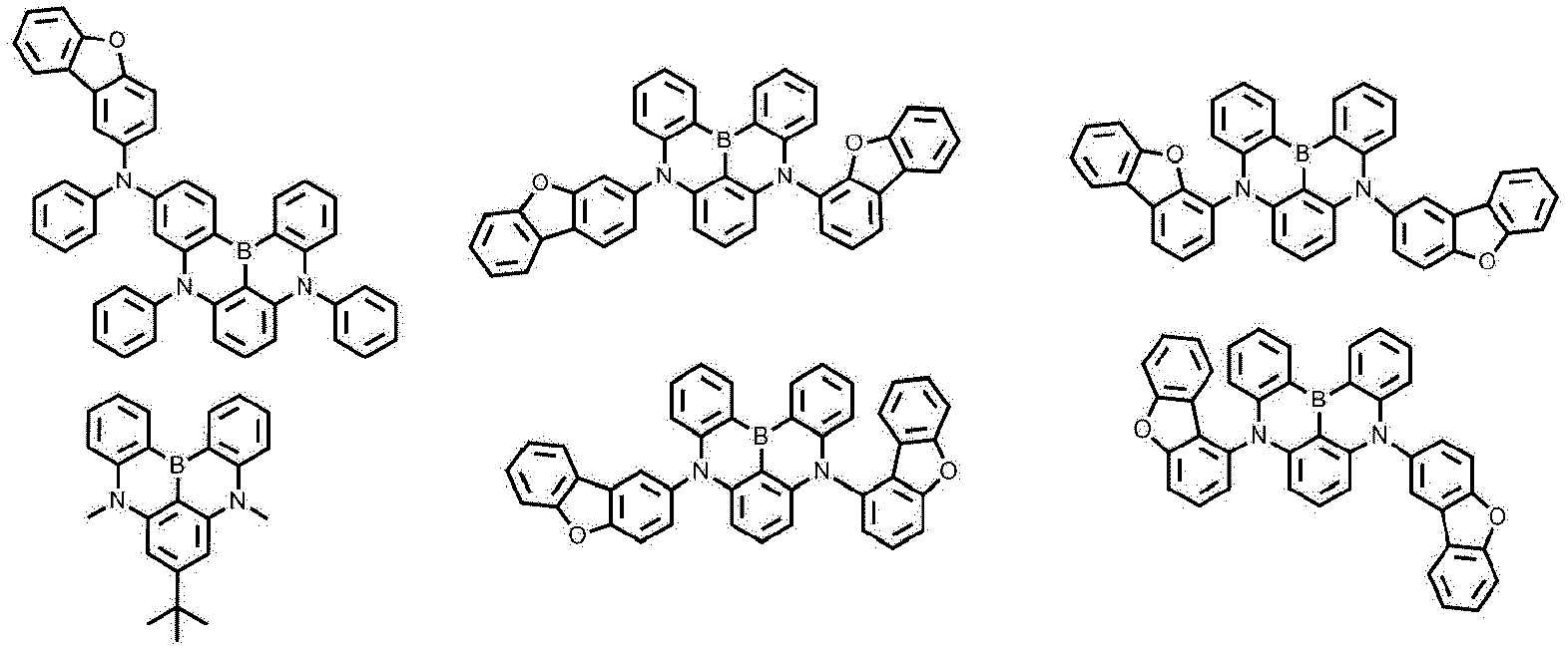


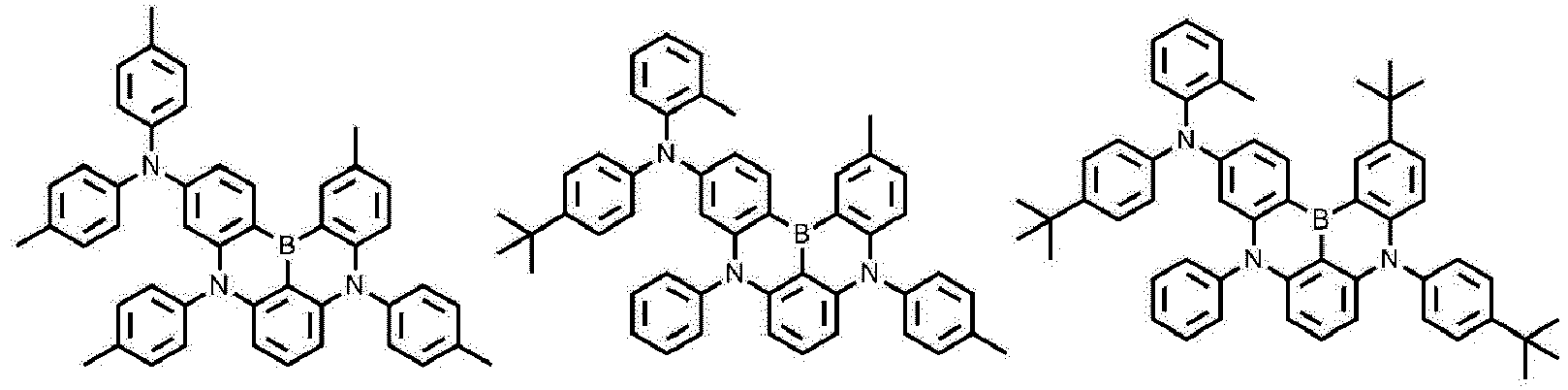


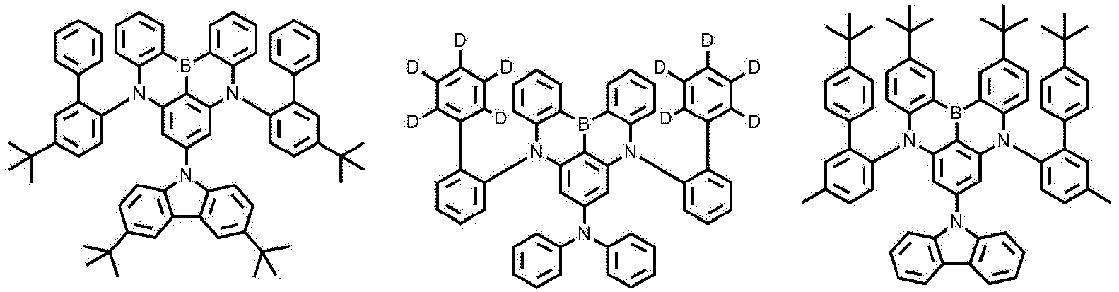
- The organic light emitting device of claim 1,
wherein the compound represented by Formula 1 is a host of the light emitting layer, and
the compound represented by Formula 2 is a dopant of the light emitting layer. - The organic light emitting device of claim 1,
wherein the compound represented by Formula 2 is comprised in an amount of 1 part by weight to 20 parts by weight based on 100 parts by weight of the compound represented by Formula 1. - The organic light emitting device of claim 1,
wherein the organic material layer further comprises one or more layers of a hole transport layer, a hole injection layer, an electron blocking layer, an electron transport and injection layer, an electron transport layer, an electron injection layer, a hole blocking layer, and a hole transport and injection layer.
Applications Claiming Priority (2)
| Application Number | Priority Date | Filing Date | Title |
|---|---|---|---|
| KR20180121874 | 2018-10-12 | ||
| PCT/KR2019/013327 WO2020076108A1 (en) | 2018-10-12 | 2019-10-11 | Organic light-emitting device |
Publications (3)
| Publication Number | Publication Date |
|---|---|
| EP3767694A1 true EP3767694A1 (en) | 2021-01-20 |
| EP3767694A4 EP3767694A4 (en) | 2021-06-09 |
| EP3767694B1 EP3767694B1 (en) | 2023-09-13 |
Family
ID=70165107
Family Applications (1)
| Application Number | Title | Priority Date | Filing Date |
|---|---|---|---|
| EP19870956.0A Active EP3767694B1 (en) | 2018-10-12 | 2019-10-11 | Organic light-emitting device |
Country Status (6)
| Country | Link |
|---|---|
| US (1) | US20210217963A1 (en) |
| EP (1) | EP3767694B1 (en) |
| JP (1) | JP7251711B2 (en) |
| KR (1) | KR102250389B1 (en) |
| CN (1) | CN112204762B (en) |
| WO (1) | WO2020076108A1 (en) |
Families Citing this family (14)
| Publication number | Priority date | Publication date | Assignee | Title |
|---|---|---|---|---|
| WO2019132040A1 (en) | 2017-12-28 | 2019-07-04 | 出光興産株式会社 | Novel compound and organic electroluminescence element |
| WO2020105990A1 (en) * | 2018-11-19 | 2020-05-28 | 에스에프씨 주식회사 | Novel boron compound and organic light-emitting device comprising same |
| KR102640485B1 (en) * | 2018-11-20 | 2024-02-26 | 에스에프씨 주식회사 | Novel boron compounds and Organic light emitting diode including the same |
| JP7187095B2 (en) * | 2019-02-20 | 2022-12-12 | エルジー・ケム・リミテッド | Anthracene derivative having dibenzofuran-1-yl or dibenzothiophen-1-yl group and organic electronic device using the same |
| JP2020188121A (en) * | 2019-05-14 | 2020-11-19 | 出光興産株式会社 | Organic electroluminescence devices and electronic devices |
| CN112047967A (en) * | 2019-06-07 | 2020-12-08 | 学校法人关西学院 | Polycyclic aromatic compound, reactive compound, polymer compound, pendant polymer compound, and uses using the same |
| CN112898322B (en) * | 2019-12-03 | 2025-02-18 | 北京鼎材科技有限公司 | An organic compound and its application and an organic electroluminescent device containing the same |
| US20210317144A1 (en) * | 2020-04-02 | 2021-10-14 | Sfc Co., Ltd. | Boron compound and organic light emitting diode including the same |
| CN115461347A (en) * | 2020-04-22 | 2022-12-09 | 三星显示有限公司 | Organic molecules for optoelectronic devices |
| WO2021230653A1 (en) * | 2020-05-12 | 2021-11-18 | 에스에프씨 주식회사 | Organic light-emitting compound and organic light-emitting device comprising same |
| CN112778343B (en) * | 2020-12-31 | 2023-07-07 | 武汉尚赛光电科技有限公司 | Boron-based organic electroluminescent material and preparation method and application thereof |
| CN113527348B (en) * | 2021-07-16 | 2024-03-29 | 京东方科技集团股份有限公司 | Compound, light-emitting layer, organic compound layer, and light-emitting device |
| CN114230597B (en) * | 2021-12-29 | 2023-12-26 | 武汉天马微电子有限公司 | An organic compound and its application |
| CN116284084B (en) * | 2023-03-14 | 2026-03-24 | 清华大学 | A luminescent material, its application, and an organic electroluminescent device comprising the same. |
Family Cites Families (16)
| Publication number | Priority date | Publication date | Assignee | Title |
|---|---|---|---|---|
| US6579630B2 (en) * | 2000-12-07 | 2003-06-17 | Canon Kabushiki Kaisha | Deuterated semiconducting organic compounds used for opto-electronic devices |
| KR20100069216A (en) * | 2008-12-16 | 2010-06-24 | 주식회사 두산 | Deuterated anthracene derivative and organic light emitting device comprising the same |
| KR101434726B1 (en) * | 2012-05-07 | 2014-08-27 | 주식회사 두산 | Anthracene derivative and organic electroluminescence device using the same |
| KR20150077586A (en) * | 2013-12-27 | 2015-07-08 | 주식회사 두산 | Organic electroluminescence device |
| TWI636056B (en) * | 2014-02-18 | 2018-09-21 | 學校法人關西學院 | Polycyclic aromatic compound and method for production the same, material for organic device and application thereof |
| US10374166B2 (en) * | 2014-02-18 | 2019-08-06 | Kwansei Gakuin Educational Foundation | Polycyclic aromatic compound |
| WO2015194839A1 (en) * | 2014-06-17 | 2015-12-23 | Rohm And Haas Electronic Materials Korea Ltd. | Electron buffering material and organic electroluminescent device |
| KR101641781B1 (en) * | 2014-09-12 | 2016-07-21 | 주식회사 엘지화학 | Organic light emitting device |
| TWI688137B (en) * | 2015-03-24 | 2020-03-11 | 學校法人關西學院 | Organic electric field light-emitting element, display device and lighting device |
| KR101781739B1 (en) * | 2015-10-07 | 2017-09-25 | 주식회사 엘지화학 | New compound and organic light emitting device comprising the same |
| KR101806464B1 (en) | 2015-11-19 | 2017-12-07 | (주)랩토 | Pyrimidine derivative substitued with pyridyl group, and organic electroluminescent device including the same |
| CN105584494B (en) | 2015-12-15 | 2017-11-24 | Ife-威奥轨道车辆门系统(青岛)有限公司 | Vehicle doorn for rail vehicle and the rail vehicle including the vehicle doorn |
| CN109155368B (en) * | 2016-04-26 | 2021-04-06 | 学校法人关西学院 | Organic electroluminescent element, display device and lighting device |
| WO2018150832A1 (en) * | 2017-02-16 | 2018-08-23 | 学校法人関西学院 | Organic electroluminescence element |
| JPWO2018186404A1 (en) * | 2017-04-03 | 2020-02-20 | 出光興産株式会社 | Organic electroluminescence device and electronic equipment |
| US20210005825A1 (en) * | 2017-04-03 | 2021-01-07 | Idemitsu Kosan Co., Ltd. | Organic electroluminescent element and electronic device |
-
2019
- 2019-10-11 CN CN201980036350.4A patent/CN112204762B/en active Active
- 2019-10-11 US US17/056,634 patent/US20210217963A1/en active Pending
- 2019-10-11 EP EP19870956.0A patent/EP3767694B1/en active Active
- 2019-10-11 KR KR1020190125966A patent/KR102250389B1/en active Active
- 2019-10-11 WO PCT/KR2019/013327 patent/WO2020076108A1/en not_active Ceased
- 2019-10-11 JP JP2020563746A patent/JP7251711B2/en active Active
Also Published As
| Publication number | Publication date |
|---|---|
| WO2020076108A1 (en) | 2020-04-16 |
| JP7251711B2 (en) | 2023-04-04 |
| KR20200041804A (en) | 2020-04-22 |
| KR102250389B1 (en) | 2021-05-11 |
| EP3767694B1 (en) | 2023-09-13 |
| CN112204762A (en) | 2021-01-08 |
| EP3767694A4 (en) | 2021-06-09 |
| US20210217963A1 (en) | 2021-07-15 |
| CN112204762B (en) | 2024-10-29 |
| JP2021525000A (en) | 2021-09-16 |
Similar Documents
| Publication | Publication Date | Title |
|---|---|---|
| EP3767694B1 (en) | Organic light-emitting device | |
| EP3757110B1 (en) | Heterocyclic compound and organic light-emitting device comprising same | |
| EP3767695B1 (en) | Organic light-emitting device | |
| CN112789273A (en) | Novel compound and organic light emitting device comprising same | |
| CN113906582B (en) | Organic light-emitting devices | |
| JP2022503628A (en) | Condensation ring compound and organic light emitting device containing it | |
| CN112105619A (en) | Polycyclic compound and organic light emitting device including the same | |
| CN113056471B (en) | Compounds and organic light-emitting diodes containing the same | |
| CN114144402A (en) | Novel compound and organic light emitting device comprising same | |
| KR20220107769A (en) | Compound and organic light emitting device comprising the same | |
| CN114206875B (en) | Compound and organic light-emitting device containing the same | |
| KR20220125018A (en) | Compound and organic light emitting device comprising same | |
| KR20220107767A (en) | Compound and organic light emitting device comprising the same | |
| CN113015733A (en) | Compound and organic light emitting device including the same | |
| CN113056468A (en) | Compound and organic light emitting device including the same | |
| CN116621842B (en) | Compound and organic light-emitting device containing the same | |
| KR102629455B1 (en) | Novel compound and organic light emitting device comprising the same | |
| CN112912365B (en) | Polycyclic compounds and organic light-emitting devices containing the same | |
| CN116419921A (en) | Compound and organic light emitting device comprising same | |
| KR20220125019A (en) | Compound and organic light emitting device comprising same | |
| KR20220107766A (en) | Compound and organic light emitting device comprising the same | |
| EP4446327B1 (en) | Compound and organic light-emitting element comprising same | |
| CN120647607A (en) | Organic compound and organic light emitting device comprising the same | |
| CN116761794A (en) | Compounds and organic light-emitting devices containing the same | |
| CN121627650A (en) | Novel compounds and organic light-emitting devices utilizing them |
Legal Events
| Date | Code | Title | Description |
|---|---|---|---|
| STAA | Information on the status of an ep patent application or granted ep patent |
Free format text: STATUS: THE INTERNATIONAL PUBLICATION HAS BEEN MADE |
|
| PUAI | Public reference made under article 153(3) epc to a published international application that has entered the european phase |
Free format text: ORIGINAL CODE: 0009012 |
|
| STAA | Information on the status of an ep patent application or granted ep patent |
Free format text: STATUS: REQUEST FOR EXAMINATION WAS MADE |
|
| 17P | Request for examination filed |
Effective date: 20201012 |
|
| AK | Designated contracting states |
Kind code of ref document: A1 Designated state(s): AL AT BE BG CH CY CZ DE DK EE ES FI FR GB GR HR HU IE IS IT LI LT LU LV MC MK MT NL NO PL PT RO RS SE SI SK SM TR |
|
| AX | Request for extension of the european patent |
Extension state: BA ME |
|
| A4 | Supplementary search report drawn up and despatched |
Effective date: 20210510 |
|
| RIC1 | Information provided on ipc code assigned before grant |
Ipc: H01L 51/54 20060101AFI20210504BHEP |
|
| DAV | Request for validation of the european patent (deleted) | ||
| DAX | Request for extension of the european patent (deleted) | ||
| REG | Reference to a national code |
Ref country code: DE Ref legal event code: R079 Free format text: PREVIOUS MAIN CLASS: H01L0051000000 Ipc: H10K0085600000 Ref country code: DE Ref legal event code: R079 Ref document number: 602019037602 Country of ref document: DE Free format text: PREVIOUS MAIN CLASS: H01L0051000000 Ipc: H10K0085600000 |
|
| GRAP | Despatch of communication of intention to grant a patent |
Free format text: ORIGINAL CODE: EPIDOSNIGR1 |
|
| STAA | Information on the status of an ep patent application or granted ep patent |
Free format text: STATUS: GRANT OF PATENT IS INTENDED |
|
| RIC1 | Information provided on ipc code assigned before grant |
Ipc: H10K 85/60 20230101AFI20230302BHEP |
|
| RIC1 | Information provided on ipc code assigned before grant |
Ipc: H10K 50/12 20230101ALN20230313BHEP Ipc: H10K 85/60 20230101AFI20230313BHEP |
|
| RIC1 | Information provided on ipc code assigned before grant |
Ipc: H10K 50/12 20230101ALN20230317BHEP Ipc: H10K 85/60 20230101AFI20230317BHEP |
|
| INTG | Intention to grant announced |
Effective date: 20230405 |
|
| GRAS | Grant fee paid |
Free format text: ORIGINAL CODE: EPIDOSNIGR3 |
|
| GRAA | (expected) grant |
Free format text: ORIGINAL CODE: 0009210 |
|
| STAA | Information on the status of an ep patent application or granted ep patent |
Free format text: STATUS: THE PATENT HAS BEEN GRANTED |
|
| AK | Designated contracting states |
Kind code of ref document: B1 Designated state(s): AL AT BE BG CH CY CZ DE DK EE ES FI FR GB GR HR HU IE IS IT LI LT LU LV MC MK MT NL NO PL PT RO RS SE SI SK SM TR |
|
| REG | Reference to a national code |
Ref country code: CH Ref legal event code: EP |
|
| REG | Reference to a national code |
Ref country code: DE Ref legal event code: R096 Ref document number: 602019037602 Country of ref document: DE |
|
| REG | Reference to a national code |
Ref country code: IE Ref legal event code: FG4D |
|
| REG | Reference to a national code |
Ref country code: LT Ref legal event code: MG9D |
|
| REG | Reference to a national code |
Ref country code: NL Ref legal event code: MP Effective date: 20230913 |
|
| PG25 | Lapsed in a contracting state [announced via postgrant information from national office to epo] |
Ref country code: GR Free format text: LAPSE BECAUSE OF FAILURE TO SUBMIT A TRANSLATION OF THE DESCRIPTION OR TO PAY THE FEE WITHIN THE PRESCRIBED TIME-LIMIT Effective date: 20231214 |
|
| PG25 | Lapsed in a contracting state [announced via postgrant information from national office to epo] |
Ref country code: SE Free format text: LAPSE BECAUSE OF FAILURE TO SUBMIT A TRANSLATION OF THE DESCRIPTION OR TO PAY THE FEE WITHIN THE PRESCRIBED TIME-LIMIT Effective date: 20230913 Ref country code: RS Free format text: LAPSE BECAUSE OF FAILURE TO SUBMIT A TRANSLATION OF THE DESCRIPTION OR TO PAY THE FEE WITHIN THE PRESCRIBED TIME-LIMIT Effective date: 20230913 Ref country code: NO Free format text: LAPSE BECAUSE OF FAILURE TO SUBMIT A TRANSLATION OF THE DESCRIPTION OR TO PAY THE FEE WITHIN THE PRESCRIBED TIME-LIMIT Effective date: 20231213 Ref country code: LV Free format text: LAPSE BECAUSE OF FAILURE TO SUBMIT A TRANSLATION OF THE DESCRIPTION OR TO PAY THE FEE WITHIN THE PRESCRIBED TIME-LIMIT Effective date: 20230913 Ref country code: LT Free format text: LAPSE BECAUSE OF FAILURE TO SUBMIT A TRANSLATION OF THE DESCRIPTION OR TO PAY THE FEE WITHIN THE PRESCRIBED TIME-LIMIT Effective date: 20230913 Ref country code: HR Free format text: LAPSE BECAUSE OF FAILURE TO SUBMIT A TRANSLATION OF THE DESCRIPTION OR TO PAY THE FEE WITHIN THE PRESCRIBED TIME-LIMIT Effective date: 20230913 Ref country code: GR Free format text: LAPSE BECAUSE OF FAILURE TO SUBMIT A TRANSLATION OF THE DESCRIPTION OR TO PAY THE FEE WITHIN THE PRESCRIBED TIME-LIMIT Effective date: 20231214 Ref country code: FI Free format text: LAPSE BECAUSE OF FAILURE TO SUBMIT A TRANSLATION OF THE DESCRIPTION OR TO PAY THE FEE WITHIN THE PRESCRIBED TIME-LIMIT Effective date: 20230913 |
|
| REG | Reference to a national code |
Ref country code: AT Ref legal event code: MK05 Ref document number: 1612634 Country of ref document: AT Kind code of ref document: T Effective date: 20230913 |
|
| PG25 | Lapsed in a contracting state [announced via postgrant information from national office to epo] |
Ref country code: NL Free format text: LAPSE BECAUSE OF FAILURE TO SUBMIT A TRANSLATION OF THE DESCRIPTION OR TO PAY THE FEE WITHIN THE PRESCRIBED TIME-LIMIT Effective date: 20230913 |
|
| PG25 | Lapsed in a contracting state [announced via postgrant information from national office to epo] |
Ref country code: IS Free format text: LAPSE BECAUSE OF FAILURE TO SUBMIT A TRANSLATION OF THE DESCRIPTION OR TO PAY THE FEE WITHIN THE PRESCRIBED TIME-LIMIT Effective date: 20240113 |
|
| PG25 | Lapsed in a contracting state [announced via postgrant information from national office to epo] |
Ref country code: AT Free format text: LAPSE BECAUSE OF FAILURE TO SUBMIT A TRANSLATION OF THE DESCRIPTION OR TO PAY THE FEE WITHIN THE PRESCRIBED TIME-LIMIT Effective date: 20230913 |
|
| PG25 | Lapsed in a contracting state [announced via postgrant information from national office to epo] |
Ref country code: ES Free format text: LAPSE BECAUSE OF FAILURE TO SUBMIT A TRANSLATION OF THE DESCRIPTION OR TO PAY THE FEE WITHIN THE PRESCRIBED TIME-LIMIT Effective date: 20230913 |
|
| PG25 | Lapsed in a contracting state [announced via postgrant information from national office to epo] |
Ref country code: SM Free format text: LAPSE BECAUSE OF FAILURE TO SUBMIT A TRANSLATION OF THE DESCRIPTION OR TO PAY THE FEE WITHIN THE PRESCRIBED TIME-LIMIT Effective date: 20230913 Ref country code: RO Free format text: LAPSE BECAUSE OF FAILURE TO SUBMIT A TRANSLATION OF THE DESCRIPTION OR TO PAY THE FEE WITHIN THE PRESCRIBED TIME-LIMIT Effective date: 20230913 Ref country code: IS Free format text: LAPSE BECAUSE OF FAILURE TO SUBMIT A TRANSLATION OF THE DESCRIPTION OR TO PAY THE FEE WITHIN THE PRESCRIBED TIME-LIMIT Effective date: 20240113 Ref country code: ES Free format text: LAPSE BECAUSE OF FAILURE TO SUBMIT A TRANSLATION OF THE DESCRIPTION OR TO PAY THE FEE WITHIN THE PRESCRIBED TIME-LIMIT Effective date: 20230913 Ref country code: EE Free format text: LAPSE BECAUSE OF FAILURE TO SUBMIT A TRANSLATION OF THE DESCRIPTION OR TO PAY THE FEE WITHIN THE PRESCRIBED TIME-LIMIT Effective date: 20230913 Ref country code: CZ Free format text: LAPSE BECAUSE OF FAILURE TO SUBMIT A TRANSLATION OF THE DESCRIPTION OR TO PAY THE FEE WITHIN THE PRESCRIBED TIME-LIMIT Effective date: 20230913 Ref country code: AT Free format text: LAPSE BECAUSE OF FAILURE TO SUBMIT A TRANSLATION OF THE DESCRIPTION OR TO PAY THE FEE WITHIN THE PRESCRIBED TIME-LIMIT Effective date: 20230913 Ref country code: SK Free format text: LAPSE BECAUSE OF FAILURE TO SUBMIT A TRANSLATION OF THE DESCRIPTION OR TO PAY THE FEE WITHIN THE PRESCRIBED TIME-LIMIT Effective date: 20230913 Ref country code: PT Free format text: LAPSE BECAUSE OF FAILURE TO SUBMIT A TRANSLATION OF THE DESCRIPTION OR TO PAY THE FEE WITHIN THE PRESCRIBED TIME-LIMIT Effective date: 20240115 |
|
| PG25 | Lapsed in a contracting state [announced via postgrant information from national office to epo] |
Ref country code: PL Free format text: LAPSE BECAUSE OF FAILURE TO SUBMIT A TRANSLATION OF THE DESCRIPTION OR TO PAY THE FEE WITHIN THE PRESCRIBED TIME-LIMIT Effective date: 20230913 Ref country code: IT Free format text: LAPSE BECAUSE OF FAILURE TO SUBMIT A TRANSLATION OF THE DESCRIPTION OR TO PAY THE FEE WITHIN THE PRESCRIBED TIME-LIMIT Effective date: 20230913 |
|
| REG | Reference to a national code |
Ref country code: CH Ref legal event code: PL |
|
| REG | Reference to a national code |
Ref country code: DE Ref legal event code: R097 Ref document number: 602019037602 Country of ref document: DE |
|
| REG | Reference to a national code |
Ref country code: BE Ref legal event code: MM Effective date: 20231031 |
|
| PG25 | Lapsed in a contracting state [announced via postgrant information from national office to epo] |
Ref country code: LU Free format text: LAPSE BECAUSE OF NON-PAYMENT OF DUE FEES Effective date: 20231011 |
|
| PG25 | Lapsed in a contracting state [announced via postgrant information from national office to epo] |
Ref country code: LU Free format text: LAPSE BECAUSE OF NON-PAYMENT OF DUE FEES Effective date: 20231011 |
|
| PG25 | Lapsed in a contracting state [announced via postgrant information from national office to epo] |
Ref country code: MC Free format text: LAPSE BECAUSE OF FAILURE TO SUBMIT A TRANSLATION OF THE DESCRIPTION OR TO PAY THE FEE WITHIN THE PRESCRIBED TIME-LIMIT Effective date: 20230913 |
|
| PG25 | Lapsed in a contracting state [announced via postgrant information from national office to epo] |
Ref country code: DK Free format text: LAPSE BECAUSE OF FAILURE TO SUBMIT A TRANSLATION OF THE DESCRIPTION OR TO PAY THE FEE WITHIN THE PRESCRIBED TIME-LIMIT Effective date: 20230913 |
|
| PG25 | Lapsed in a contracting state [announced via postgrant information from national office to epo] |
Ref country code: CH Free format text: LAPSE BECAUSE OF NON-PAYMENT OF DUE FEES Effective date: 20231031 |
|
| PLBE | No opposition filed within time limit |
Free format text: ORIGINAL CODE: 0009261 |
|
| STAA | Information on the status of an ep patent application or granted ep patent |
Free format text: STATUS: NO OPPOSITION FILED WITHIN TIME LIMIT |
|
| PG25 | Lapsed in a contracting state [announced via postgrant information from national office to epo] |
Ref country code: MC Free format text: LAPSE BECAUSE OF FAILURE TO SUBMIT A TRANSLATION OF THE DESCRIPTION OR TO PAY THE FEE WITHIN THE PRESCRIBED TIME-LIMIT Effective date: 20230913 Ref country code: DK Free format text: LAPSE BECAUSE OF FAILURE TO SUBMIT A TRANSLATION OF THE DESCRIPTION OR TO PAY THE FEE WITHIN THE PRESCRIBED TIME-LIMIT Effective date: 20230913 Ref country code: CH Free format text: LAPSE BECAUSE OF NON-PAYMENT OF DUE FEES Effective date: 20231031 |
|
| 26N | No opposition filed |
Effective date: 20240614 |
|
| PG25 | Lapsed in a contracting state [announced via postgrant information from national office to epo] |
Ref country code: BE Free format text: LAPSE BECAUSE OF NON-PAYMENT OF DUE FEES Effective date: 20231031 |
|
| PG25 | Lapsed in a contracting state [announced via postgrant information from national office to epo] |
Ref country code: IE Free format text: LAPSE BECAUSE OF NON-PAYMENT OF DUE FEES Effective date: 20231011 |
|
| PG25 | Lapsed in a contracting state [announced via postgrant information from national office to epo] |
Ref country code: SI Free format text: LAPSE BECAUSE OF FAILURE TO SUBMIT A TRANSLATION OF THE DESCRIPTION OR TO PAY THE FEE WITHIN THE PRESCRIBED TIME-LIMIT Effective date: 20230913 |
|
| PG25 | Lapsed in a contracting state [announced via postgrant information from national office to epo] |
Ref country code: SI Free format text: LAPSE BECAUSE OF FAILURE TO SUBMIT A TRANSLATION OF THE DESCRIPTION OR TO PAY THE FEE WITHIN THE PRESCRIBED TIME-LIMIT Effective date: 20230913 Ref country code: IE Free format text: LAPSE BECAUSE OF NON-PAYMENT OF DUE FEES Effective date: 20231011 |
|
| PG25 | Lapsed in a contracting state [announced via postgrant information from national office to epo] |
Ref country code: BG Free format text: LAPSE BECAUSE OF FAILURE TO SUBMIT A TRANSLATION OF THE DESCRIPTION OR TO PAY THE FEE WITHIN THE PRESCRIBED TIME-LIMIT Effective date: 20230913 |
|
| PG25 | Lapsed in a contracting state [announced via postgrant information from national office to epo] |
Ref country code: BG Free format text: LAPSE BECAUSE OF FAILURE TO SUBMIT A TRANSLATION OF THE DESCRIPTION OR TO PAY THE FEE WITHIN THE PRESCRIBED TIME-LIMIT Effective date: 20230913 |
|
| PG25 | Lapsed in a contracting state [announced via postgrant information from national office to epo] |
Ref country code: CY Free format text: LAPSE BECAUSE OF FAILURE TO SUBMIT A TRANSLATION OF THE DESCRIPTION OR TO PAY THE FEE WITHIN THE PRESCRIBED TIME-LIMIT; INVALID AB INITIO Effective date: 20191011 |
|
| PG25 | Lapsed in a contracting state [announced via postgrant information from national office to epo] |
Ref country code: HU Free format text: LAPSE BECAUSE OF FAILURE TO SUBMIT A TRANSLATION OF THE DESCRIPTION OR TO PAY THE FEE WITHIN THE PRESCRIBED TIME-LIMIT; INVALID AB INITIO Effective date: 20191011 |
|
| PGFP | Annual fee paid to national office [announced via postgrant information from national office to epo] |
Ref country code: GB Payment date: 20250922 Year of fee payment: 7 |
|
| PGFP | Annual fee paid to national office [announced via postgrant information from national office to epo] |
Ref country code: FR Payment date: 20250925 Year of fee payment: 7 |
|
| PG25 | Lapsed in a contracting state [announced via postgrant information from national office to epo] |
Ref country code: TR Free format text: LAPSE BECAUSE OF FAILURE TO SUBMIT A TRANSLATION OF THE DESCRIPTION OR TO PAY THE FEE WITHIN THE PRESCRIBED TIME-LIMIT Effective date: 20230913 |
|
| PGFP | Annual fee paid to national office [announced via postgrant information from national office to epo] |
Ref country code: DE Payment date: 20250922 Year of fee payment: 7 |