EP3767681A2 - Electroluminescent device - Google Patents
Electroluminescent device Download PDFInfo
- Publication number
- EP3767681A2 EP3767681A2 EP20186084.8A EP20186084A EP3767681A2 EP 3767681 A2 EP3767681 A2 EP 3767681A2 EP 20186084 A EP20186084 A EP 20186084A EP 3767681 A2 EP3767681 A2 EP 3767681A2
- Authority
- EP
- European Patent Office
- Prior art keywords
- effective
- pinhole
- light blocking
- electroluminescent device
- optical center
- Prior art date
- Legal status (The legal status is an assumption and is not a legal conclusion. Google has not performed a legal analysis and makes no representation as to the accuracy of the status listed.)
- Pending
Links
Images












Classifications
-
- G—PHYSICS
- G06—COMPUTING OR CALCULATING; COUNTING
- G06V—IMAGE OR VIDEO RECOGNITION OR UNDERSTANDING
- G06V40/00—Recognition of biometric, human-related or animal-related patterns in image or video data
- G06V40/10—Human or animal bodies, e.g. vehicle occupants or pedestrians; Body parts, e.g. hands
- G06V40/12—Fingerprints or palmprints
- G06V40/13—Sensors therefor
- G06V40/1318—Sensors therefor using electro-optical elements or layers, e.g. electroluminescent sensing
-
- G—PHYSICS
- G02—OPTICS
- G02B—OPTICAL ELEMENTS, SYSTEMS OR APPARATUS
- G02B26/00—Optical devices or arrangements for the control of light using movable or deformable optical elements
- G02B26/004—Optical devices or arrangements for the control of light using movable or deformable optical elements based on a displacement or a deformation of a fluid
- G02B26/005—Optical devices or arrangements for the control of light using movable or deformable optical elements based on a displacement or a deformation of a fluid based on electrowetting
-
- G—PHYSICS
- G02—OPTICS
- G02F—OPTICAL DEVICES OR ARRANGEMENTS FOR THE CONTROL OF LIGHT BY MODIFICATION OF THE OPTICAL PROPERTIES OF THE MEDIA OF THE ELEMENTS INVOLVED THEREIN; NON-LINEAR OPTICS; FREQUENCY-CHANGING OF LIGHT; OPTICAL LOGIC ELEMENTS; OPTICAL ANALOGUE/DIGITAL CONVERTERS
- G02F1/00—Devices or arrangements for the control of the intensity, colour, phase, polarisation or direction of light arriving from an independent light source, e.g. switching, gating or modulating; Non-linear optics
- G02F1/01—Devices or arrangements for the control of the intensity, colour, phase, polarisation or direction of light arriving from an independent light source, e.g. switching, gating or modulating; Non-linear optics for the control of the intensity, phase, polarisation or colour
- G02F1/13—Devices or arrangements for the control of the intensity, colour, phase, polarisation or direction of light arriving from an independent light source, e.g. switching, gating or modulating; Non-linear optics for the control of the intensity, phase, polarisation or colour based on liquid crystals, e.g. single liquid crystal display cells
- G02F1/133—Constructional arrangements; Operation of liquid crystal cells; Circuit arrangements
- G02F1/1333—Constructional arrangements; Manufacturing methods
- G02F1/13338—Input devices, e.g. touch panels
-
- G—PHYSICS
- G02—OPTICS
- G02F—OPTICAL DEVICES OR ARRANGEMENTS FOR THE CONTROL OF LIGHT BY MODIFICATION OF THE OPTICAL PROPERTIES OF THE MEDIA OF THE ELEMENTS INVOLVED THEREIN; NON-LINEAR OPTICS; FREQUENCY-CHANGING OF LIGHT; OPTICAL LOGIC ELEMENTS; OPTICAL ANALOGUE/DIGITAL CONVERTERS
- G02F1/00—Devices or arrangements for the control of the intensity, colour, phase, polarisation or direction of light arriving from an independent light source, e.g. switching, gating or modulating; Non-linear optics
- G02F1/01—Devices or arrangements for the control of the intensity, colour, phase, polarisation or direction of light arriving from an independent light source, e.g. switching, gating or modulating; Non-linear optics for the control of the intensity, phase, polarisation or colour
- G02F1/15—Devices or arrangements for the control of the intensity, colour, phase, polarisation or direction of light arriving from an independent light source, e.g. switching, gating or modulating; Non-linear optics for the control of the intensity, phase, polarisation or colour based on an electrochromic effect
-
- G—PHYSICS
- G06—COMPUTING OR CALCULATING; COUNTING
- G06F—ELECTRIC DIGITAL DATA PROCESSING
- G06F3/00—Input arrangements for transferring data to be processed into a form capable of being handled by the computer; Output arrangements for transferring data from processing unit to output unit, e.g. interface arrangements
- G06F3/01—Input arrangements or combined input and output arrangements for interaction between user and computer
- G06F3/03—Arrangements for converting the position or the displacement of a member into a coded form
- G06F3/041—Digitisers, e.g. for touch screens or touch pads, characterised by the transducing means
- G06F3/042—Digitisers, e.g. for touch screens or touch pads, characterised by the transducing means by opto-electronic means
- G06F3/0421—Digitisers, e.g. for touch screens or touch pads, characterised by the transducing means by opto-electronic means by interrupting or reflecting a light beam, e.g. optical touch-screen
-
- G—PHYSICS
- G06—COMPUTING OR CALCULATING; COUNTING
- G06V—IMAGE OR VIDEO RECOGNITION OR UNDERSTANDING
- G06V40/00—Recognition of biometric, human-related or animal-related patterns in image or video data
- G06V40/10—Human or animal bodies, e.g. vehicle occupants or pedestrians; Body parts, e.g. hands
- G06V40/12—Fingerprints or palmprints
- G06V40/13—Sensors therefor
-
- H—ELECTRICITY
- H05—ELECTRIC TECHNIQUES NOT OTHERWISE PROVIDED FOR
- H05B—ELECTRIC HEATING; ELECTRIC LIGHT SOURCES NOT OTHERWISE PROVIDED FOR; CIRCUIT ARRANGEMENTS FOR ELECTRIC LIGHT SOURCES, IN GENERAL
- H05B33/00—Electroluminescent light sources
- H05B33/12—Light sources with substantially two-dimensional [2D] radiating surfaces
-
- H—ELECTRICITY
- H10—SEMICONDUCTOR DEVICES; ELECTRIC SOLID-STATE DEVICES NOT OTHERWISE PROVIDED FOR
- H10F—INORGANIC SEMICONDUCTOR DEVICES SENSITIVE TO INFRARED RADIATION, LIGHT, ELECTROMAGNETIC RADIATION OF SHORTER WAVELENGTH OR CORPUSCULAR RADIATION
- H10F39/00—Integrated devices, or assemblies of multiple devices, comprising at least one element covered by group H10F30/00, e.g. radiation detectors comprising photodiode arrays
- H10F39/10—Integrated devices
- H10F39/12—Image sensors
-
- H—ELECTRICITY
- H10—SEMICONDUCTOR DEVICES; ELECTRIC SOLID-STATE DEVICES NOT OTHERWISE PROVIDED FOR
- H10K—ORGANIC ELECTRIC SOLID-STATE DEVICES
- H10K50/00—Organic light-emitting devices
- H10K50/10—OLEDs or polymer light-emitting diodes [PLED]
- H10K50/11—OLEDs or polymer light-emitting diodes [PLED] characterised by the electroluminescent [EL] layers
-
- H—ELECTRICITY
- H10—SEMICONDUCTOR DEVICES; ELECTRIC SOLID-STATE DEVICES NOT OTHERWISE PROVIDED FOR
- H10K—ORGANIC ELECTRIC SOLID-STATE DEVICES
- H10K50/00—Organic light-emitting devices
- H10K50/80—Constructional details
- H10K50/86—Arrangements for improving contrast, e.g. preventing reflection of ambient light
- H10K50/865—Arrangements for improving contrast, e.g. preventing reflection of ambient light comprising light absorbing layers, e.g. light-blocking layers
-
- H—ELECTRICITY
- H10—SEMICONDUCTOR DEVICES; ELECTRIC SOLID-STATE DEVICES NOT OTHERWISE PROVIDED FOR
- H10K—ORGANIC ELECTRIC SOLID-STATE DEVICES
- H10K59/00—Integrated devices, or assemblies of multiple devices, comprising at least one organic light-emitting element covered by group H10K50/00
- H10K59/10—OLED displays
- H10K59/12—Active-matrix OLED [AMOLED] displays
-
- H—ELECTRICITY
- H10—SEMICONDUCTOR DEVICES; ELECTRIC SOLID-STATE DEVICES NOT OTHERWISE PROVIDED FOR
- H10K—ORGANIC ELECTRIC SOLID-STATE DEVICES
- H10K59/00—Integrated devices, or assemblies of multiple devices, comprising at least one organic light-emitting element covered by group H10K50/00
- H10K59/10—OLED displays
- H10K59/12—Active-matrix OLED [AMOLED] displays
- H10K59/122—Pixel-defining structures or layers, e.g. banks
-
- H—ELECTRICITY
- H10—SEMICONDUCTOR DEVICES; ELECTRIC SOLID-STATE DEVICES NOT OTHERWISE PROVIDED FOR
- H10K—ORGANIC ELECTRIC SOLID-STATE DEVICES
- H10K59/00—Integrated devices, or assemblies of multiple devices, comprising at least one organic light-emitting element covered by group H10K50/00
- H10K59/10—OLED displays
- H10K59/12—Active-matrix OLED [AMOLED] displays
- H10K59/126—Shielding, e.g. light-blocking means over the TFTs
-
- H—ELECTRICITY
- H10—SEMICONDUCTOR DEVICES; ELECTRIC SOLID-STATE DEVICES NOT OTHERWISE PROVIDED FOR
- H10K—ORGANIC ELECTRIC SOLID-STATE DEVICES
- H10K59/00—Integrated devices, or assemblies of multiple devices, comprising at least one organic light-emitting element covered by group H10K50/00
- H10K59/40—OLEDs integrated with touch screens
-
- H—ELECTRICITY
- H10—SEMICONDUCTOR DEVICES; ELECTRIC SOLID-STATE DEVICES NOT OTHERWISE PROVIDED FOR
- H10K—ORGANIC ELECTRIC SOLID-STATE DEVICES
- H10K59/00—Integrated devices, or assemblies of multiple devices, comprising at least one organic light-emitting element covered by group H10K50/00
- H10K59/60—OLEDs integrated with inorganic light-sensitive elements, e.g. with inorganic solar cells or inorganic photodiodes
-
- H—ELECTRICITY
- H10—SEMICONDUCTOR DEVICES; ELECTRIC SOLID-STATE DEVICES NOT OTHERWISE PROVIDED FOR
- H10K—ORGANIC ELECTRIC SOLID-STATE DEVICES
- H10K59/00—Integrated devices, or assemblies of multiple devices, comprising at least one organic light-emitting element covered by group H10K50/00
- H10K59/60—OLEDs integrated with inorganic light-sensitive elements, e.g. with inorganic solar cells or inorganic photodiodes
- H10K59/65—OLEDs integrated with inorganic image sensors
-
- H—ELECTRICITY
- H10—SEMICONDUCTOR DEVICES; ELECTRIC SOLID-STATE DEVICES NOT OTHERWISE PROVIDED FOR
- H10K—ORGANIC ELECTRIC SOLID-STATE DEVICES
- H10K59/00—Integrated devices, or assemblies of multiple devices, comprising at least one organic light-emitting element covered by group H10K50/00
- H10K59/80—Constructional details
- H10K59/8791—Arrangements for improving contrast, e.g. preventing reflection of ambient light
- H10K59/8792—Arrangements for improving contrast, e.g. preventing reflection of ambient light comprising light absorbing layers, e.g. black layers
-
- H—ELECTRICITY
- H10—SEMICONDUCTOR DEVICES; ELECTRIC SOLID-STATE DEVICES NOT OTHERWISE PROVIDED FOR
- H10K—ORGANIC ELECTRIC SOLID-STATE DEVICES
- H10K59/00—Integrated devices, or assemblies of multiple devices, comprising at least one organic light-emitting element covered by group H10K50/00
- H10K59/80—Constructional details
- H10K59/88—Dummy elements, i.e. elements having non-functional features
-
- G—PHYSICS
- G06—COMPUTING OR CALCULATING; COUNTING
- G06F—ELECTRIC DIGITAL DATA PROCESSING
- G06F2203/00—Indexing scheme relating to G06F3/00 - G06F3/048
- G06F2203/041—Indexing scheme relating to G06F3/041 - G06F3/045
- G06F2203/04111—Cross over in capacitive digitiser, i.e. details of structures for connecting electrodes of the sensing pattern where the connections cross each other, e.g. bridge structures comprising an insulating layer, or vias through substrate
Definitions
- embodiments of the present disclosure are directed to an electroluminescent device. More particularly, embodiments of the present disclosure are directed to an electroluminescent device that includes a fingerprint sensor.
- An electroluminescent device has a fast response speed and high luminous efficiency, luminance and field of view by using a self-emitting light emitting diode. Recently, as electroluminescent devices such as smartphones and tablet PCs are used in various ways, biometric information authentication methods that use fingerprints, etc., of a user have become widely used. To provide a fingerprint sensing function, an electroluminescent device is provided with a fingerprint sensor in such a way that the fingerprint sensor is installed in or mounted to the electroluminescent device.
- the fingerprint sensor can be configured as a photo-sensing type sensor.
- a photo-sensing fingerprint sensor includes a light source, a lens, and an optical sensor array. If a fingerprint sensor is attached to a luminous panel, the thickness of the electroluminescent device may increase, and the production cost of the electroluminescent device may increase.
- Various embodiments of the present disclosure are directed to an electroluminescent device that is thinner than previous devices while improving reliability.
- An aspect of the present disclosure provides an electroluminescent device, comprising a first insulation layer, an electroluminescent structure that includes lower electrodes disposed on the first insulation layer, luminous layers disposed on the lower electrodes, and an upper electrode disposed on the luminous layers, a first light blocking structure disposed under the first insulation layer and that includes first effective pinholes, and an image sensor structure disposed under the first light blocking structure and that includes effective image sensors that overlap the first effective pinholes.
- the lower electrodes do not overlap the first effective pinholes.
- the first light blocking structure further comprises first dummy pinholes.
- the first dummy pinhole is located between the first effective pinholes, and the first effective pinholes and the first dummy pinholes form a single grid arrangement in plan view.
- the electroluminescent device further comprises a second light blocking structure disposed between the first light blocking structure and the image sensor structure, and that includes a second light blocking area and second effective pinholes.
- the second light blocking area does not overlap the first effective pinholes and blocks light passing through the first dummy pinholes, and the second effective pinholes overlap the first effective pinholes.
- the electroluminescent device further comprises a second light blocking structure disposed between the first light blocking structure and the image sensor structure, and that includes a second light blocking area and second effective pinholes.
- the second light blocking area does not overlap the first effective pinholes, and the second effective pinholes overlap the first effective pinholes.
- the second light blocking area includes an additional pinhole.
- the electroluminescent device further comprises a light blocking member provided over or under the additional pinhole and overlapping the additional pinhole.
- the additional pinhole is smaller than the second effective pinhole.
- a shortest plane distance from an optical center of the first effective pinhole to the lower electrodes is greater than a plane distance measured from the optical center of the first effective pinhole to an inner wall of the first effective pinhole in a first direction in which the shortest plane distance from the optical center of the first effective pinhole to the lower electrodes is measured.
- the lower electrodes include a single first lower electrode that is firstly closest in plan view to the optical center of the first effective pinhole, and a single second lower electrode that is secondly closest in plan view to the optical center of the first effective pinhole.
- a shortest plane distance from the optical center of the first effective pinhole to the single second lower electrode is measured in a second direction, and an angle between the first and second directions is not k ⁇ 180°, where k is integers other than zero.
- the lower electrodes include a single first lower electrode that is firstly closest in plan view to the optical center of the first effective pinhole, and at least two second lower electrodes that are secondly closest in plan view to the optical center of the first effective pinhole.
- the lower electrodes include at least two first lower electrodes that are firstly closest in plan view to the optical center of the first effective pinhole.
- the electroluminescent device further comprises a pixel defining layer disposed on the first insulation layer and that covers edges of the lower electrodes, and spacers disposed on the pixel defining layer to be higher than the pixel defining layer.
- a shortest plane distance from the optical center of the first effective pinhole to the spacers is greater than the shortest plane distance from the optical center of the first effective pinhole to the lower electrodes.
- the electroluminescent device further comprises a touch sensing structure including touch sensing electrodes and bridges, and located above the electroluminescent structure.
- the bridge electrically couples two neighboring touch sensing electrodes to each other, and a shortest plane distance from the optical center of the first effective pinhole to the bridges is greater than the shortest plane distance from the optical center of the first effective pinhole to the spacers.
- the electroluminescent device further comprises a pixel defining layer disposed on the first insulation layer and that covers edges of the lower electrodes, and spacers disposed on the pixel defining layer to be higher than the pixel defining layer.
- a shortest plane distance from the optical center of the first effective pinhole to the spacers is greater than a plane distance measured from the optical center of the first effective pinhole to an inner wall of the first effective pinhole in a third direction in which the shortest plane distance from the optical center of the first effective pinhole to the spacers is measured.
- the spacers include a single first spacer that is firstly closest in plan view to the optical center of the first effective pinhole, and a single second spacer that is secondly closest in plan view to the optical center of the first effective pinhole.
- a shortest plane distance from the optical center of the first effective pinhole to the second spacer is measured in a fourth direction, and the third and fourth directions form a single second angle, and the second angle is not m ⁇ 180°, where m is integers other than zero.
- the spacers include a single first spacer that is firstly closest in plan view to the optical center of the first effective pinhole, and at least two second spacers that are secondly closest in plan view to the optical center of the first effective pinhole.
- the spacers include at least two first spacers that are firstly closest in plan view to the optical center of the first effective pinhole.
- the electroluminescent device further comprises a touch sensing structure that includes touch sensing electrodes and bridges, and is located above the electroluminescent structure.
- the bridge electrically couples two neighboring touch sensing electrodes to each other, and a shortest plane distance from the optical center of the first effective pinhole to the bridges is greater than the shortest plane distance from the optical center of the first effective pinhole to the spacers.
- the electroluminescent device further comprises a touch sensing structure that includes touch sensing electrodes and bridges, and is located above the electroluminescent structure.
- the bridge electrically couples two neighboring touch sensing electrodes to each other, and a shortest plane distance from the optical center of the first effective pinhole to the bridges is greater than a plane distance measured from the optical center of the first effective pinhole to an inner wall of the first effective pinhole in a fifth direction in which the shortest plane distance from the optical center of the first effective pinhole to the bridges is measured.
- the bridges include a single first bridge that is firstly closest in plan view to the optical center of the first effective pinhole, and a single second bridge that is secondly closest in plan view to the optical center of the first effective pinhole.
- a shortest plane distance from the optical center of the first effective pinhole to the single second bridge is measured in a sixth direction, and the fifth and sixth directions form a third angle, and the third angle is n ⁇ 180°, where n is integers other than zero.
- the bridges include a single first bridge that is firstly closest in plan view to the optical center of the first effective pinhole, and at least two second bridges that are secondly closest in plan view to the optical center of the first effective pinhole.
- the bridges include at least two first bridges that are firstly closest in plan view to the optical center of the first effective pinhole.
- the electroluminescent device further comprises a touch sensing structure that includes bridges and touch sensing electrodes disposed on a different layer from the bridges, and that is located above the electroluminescent structure.
- the bridge electrically couples two neighboring touch sensing electrodes to each other, the bridges include overlap areas that overlap the touch sensing electrodes, and a shortest plane distance from the optical center of the first effective pinhole to the overlap areas is greater than a plane distance measured from the optical center of the first effective pinhole to an inner wall of the first effective pinhole in a direction in which the shortest plane distance from the optical center of the first effective pinhole to the overlap areas is measured.
- the electroluminescent structure has overlap areas where at least two luminous layers overlap, and the first effective pinhole overlaps the overlap area.
- the electroluminescent device further comprises a pixel defining layer disposed on the first insulation layer and that covers edges of the lower electrodes, and spacers disposed on the pixel defining layer to be higher than the pixel defining layer.
- the overlap area does not overlap the spacers.
- the electroluminescent device further comprises a pixel defining layer disposed on the first insulation layer and that covers edges of the lower electrodes, and spacers disposed on the pixel defining layer to be higher than the pixel defining layer.
- the spacer has a curved edge between side and upper surfaces of the spacer in a cross-section, the spacer has a curved edge in plan view, and the spacer overlaps the first effective pinhole.
- the image sensor structure further includes a dummy image sensor located between the effective image sensors.
- An aspect of the present disclosure provides an electroluminescent device, comprising an electroluminescent structure that includes lower electrodes disposed on an insulation layer, luminous layers disposed on the lower electrodes, and an upper electrode disposed on the luminous layers, a first light blocking structure located on a same layer as the lower electrodes, and an image sensor structure located under the insulation layer and that includes effective image sensors.
- the electroluminescent structure includes luminous areas where the lower electrodes, the luminous layers and the upper electrode overlap each other to emit light
- the first light blocking structure includes a first effective pinhole that overlaps the effective image sensor.
- the first light blocking structure is integrally formed with the lower electrode as a single piece.
- the first light blocking structure is not electrically coupled to the lower electrodes, the first light blocking structure has a shape of an island that does not surround the lower electrode, and the first light blocking structure is provided in plurality.
- the first light blocking structure is electrically coupled to the upper electrode.
- the first light blocking structure is not electrically coupled to the lower electrodes, the first light blocking structure has a mesh shape with a hole, and the hole surrounds the lower electrode.
- the first light blocking structure is electrically coupled to the upper electrode.
- the electroluminescent device further comprises a second light blocking structure located between the first light blocking structure and the image sensor structure, and that includes second effective pinholes.
- the first effective pinhole overlaps the second effective pinhole, and the first effective pinhole is smaller than the second effective pinhole.
- An aspect of the present disclosure provides an electroluminescent device, comprising an electroluminescent structure that includes lower electrodes, luminous layers disposed on the lower electrodes, and an upper electrode disposed on the luminous layers, a light blocking structure disposed under the electroluminescent structure and that includes effective pinholes, an image sensor structure disposed under the light blocking structure and that includes image sensors that overlap the effective pinholes, and a touch sensing structure that includes touch sensing electrodes and bridges and that is located above the electroluminescent structure.
- the lower electrodes do not overlap the effective pinholes
- the bridge electrically couples two neighboring touch sensing electrodes to each other, and at least one of the touch sensing electrode and/or the bridge includes at least one opening that overlaps the effective pinholes.
- the electroluminescent structure comprises luminous areas where the lower electrodes, the luminous layers and the upper electrode overlap each other to emit light
- the at least one of the touch sensing electrode and/or the bridge further includes a hole that overlaps the luminous area, and a size of the opening is greater than a size of the hole.
- an electroluminescent device as set out in claim 1. Additional features are set out in claims 2 to 30. According to an aspect, there is provided an electroluminescent device as set out in claim 31. Additional features are set out in claims 30 to 37. According to an aspect, there is provided an electroluminescent device as set out in claim 38. Additional features are set out in claim 39.
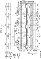
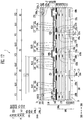
- FIGS. 1A and 1B are plan views of an electroluminescent device in accordance with an embodiment of the present disclosure. To be more specific, FIGS. 1A and 1B are plan views of an electroluminescent device that has a display area in which an image sensor is located, in accordance with an embodiment of the present disclosure.
- the electroluminescent device 1 in accordance with an embodiment of the present disclosure includes a display area DA and a non-display area NDA.
- the electroluminescent device 1 may have various shapes.
- the electroluminescent device 1 may have the shape of a flat rectangle having two pairs of parallel sides that are respectively parallel to a first direction DR1 and a second direction DR2 that is substantially perpendicular to the first direction DR1.
- the electroluminescent device 1 can display visual information in an image display direction.
- the visual information may include text, video, photographs, 3D stereoscopic images, etc.
- the electroluminescent device 1 may be entirely flexible or may be flexible only in some areas. As one example, when the electroluminescent device 1 is entirely flexible, the electroluminescent device 1 may be a rollable device. As another example, when only some areas of the electroluminescent device 1 are flexible, the electroluminescent device 1 may be a foldable device.
- the display area DA includes pixel circuits PC.
- the pixel circuit PC is electrically connected to an electroluminescent unit ELU, shown in FIG. 2 .
- the electroluminescent unit ELU and the pixel circuit PC are illustrated in FIG. 21 .
- the non-display area NDA is located on at least one side of the display area DA.
- the non-display area NDA surrounds the display area DA.
- the non-display area NDA is an area of the electroluminescent device 1 other than the display area DA.
- Peripheral wiring, peripheral circuits, pads, dummy pixels, etc., are located in the non-display area NDA.
- At least one area of the display area DA is a sensing area SA that can sense a user's fingerprint, etc.
- a sensing area SA that can sense a user's fingerprint, etc.
- only some of the display area DA is the sensing area SA.
- the whole of the display area DA is the sensing area SA.
- the non-display area NDA that surrounds the display area DA is a non-sensing area NSA.
- At least one image sensor 160a (hereinafter, also referred as effective image sensor 160a) is located within the sensing area SA.
- the electroluminescent device 1 has a first surface 1a, shown in FIG. 2 , on which the image is displayed, and a second surface 1b, shown in FIG. 2 , which is opposite to the first surface 1a, and image sensors 160a are located closer to the second surface 1b than the first surface 1a.
- the electroluminescent unit ELU connected to the pixel circuit PC, which is located in or adjacent to the sensing area SA, is used as the light source for the fingerprint sensing of the image sensor 160a.
- light EL shown in FIG. 2
- emitted from the electroluminescent unit ELU is reflected by a user's finger to be changed into reflected light RL, shown in FIG.
- both the electroluminescent unit ELU and the image sensor 160a are located in the sensing area SA. Since the electroluminescent device 1 does not use an external light source but uses the electroluminescent unit ELU as a light source, the thickness of the electroluminescent device 1 can be reduced and a manufacturing cost thereof can be reduced. However, embodiments of the present disclosure can adopt a separate external light source for sensing the fingerprint, without being limited to the above configuration.
- the image sensors 160a can perform various functions, such as those of a touch sensor, a scanner, a camera, etc., in addition to sensing a fingerprint.
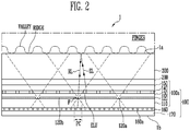
- FIG. 2 is a sectional view of an electroluminescent device illustrated in FIG. 1A or FIG. 1B in accordance with an embodiment of the present disclosure.
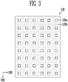
- FIG. 3 is a plan view of a light blocking structure of FIG. 2 in accordance with an embodiment of the present disclosure.
- FIG. 4 is a plan view of an electroluminescent device that includes a light blocking structure of FIG. 2 in accordance with an embodiment of the present disclosure.
- the electroluminescent device 1 includes an electroluminescent panel 100 that has an image sensor structure 160.
- the electroluminescent device 1 includes a touch sensing structure 200 located on the electroluminescent panel 100, and a window 300 located on the touch sensing structure 200.
- the electroluminescent panel 100 displays an image.
- the electroluminescent panel 100 uses current as a driving power supply.
- the electroluminescent panel 100 may be an organic electroluminescent panel or an inorganic electroluminescent panel.
- the electroluminescent device 1 may employ a luminous panel that uses voltage as the driving power supply, instead of the electroluminescent panel 100.
- the luminous panel may be a liquid crystal panel, an electrophoretic panel or an electro-wetting panel.
- the electroluminescent panel 100 includes a luminous module 100a, the image sensor structure 160, and a protective layer 170.
- the luminous module 100a includes a transparent layer 110, a light blocking structure 120, a pixel circuit structure 130, an electroluminescent structure 140, and an encapsulation structure 150.
- the transparent layer 110 may include glass, tempered glass, transparent plastics, etc., and may be rigid or flexible.
- the transparent layer 110 is a substrate.
- the expression "the transparent layer 110 is the substrate” means that stacking processes are performed on the transparent layer 110 with the transparent layer 110 being at the lowermost position, or that, after stacking processes are performed on the transparent layer 110, a structure located under the transparent layer 110 is detached from the transparent layer 110 so that the transparent layer 110 is located at the lowermost position.
- the pixel circuit structure 130 is located above the transparent layer 110.
- the pixel circuit structure 130 includes at least one conductive layer and at least one insulation layer.
- the pixel circuit structure 130 includes a pixel circuit PC that has a circuit element such as a transistor or a capacitor, and wiring connected to the pixel circuit PC, such as a signal line or a power line.
- the pixel circuit structure 130 further includes peripheral wiring located in the non-display area NDA, a peripheral circuit, etc.
- the electroluminescent structure 140 is disposed on the pixel circuit structure 130.
- the electroluminescent structure 140 includes the electroluminescent unit ELU, which is connected to the pixel circuit PC of the pixel circuit structure 130 through a contact hole.
- the encapsulation structure 150 is disposed on the electroluminescent structure 140 and covers the display area DA of at least the transparent layer 110.
- the encapsulation structure 150 includes a first inorganic layer, an organic layer on the first inorganic layer, and a second inorganic layer on the organic layer.
- the encapsulation structure 150 may be a glass layer.
- the light blocking structure 120 is located between the transparent layer 110 and the pixel circuit structure 130 in at least the sensing area SA.
- the light blocking structure 120 includes pinholes 120a (hereinafter, also referred as effective pinholes 120a) and a light blocking area 120b.
- the light blocking area 120b includes a light blocking material that can absorb or reflect light.
- the light blocking area 120b includes an opaque metal.
- the pinhole 120a is a through hole. A focus F of the reflected light RL is located in the pinhole 120a.
- the pinholes 120a are the same size.
- a width of the pinhole 120a is approximately ten times or more the wavelength of incident light so as to prevent diffraction of the light.
- the sizes of the pinholes 120a may differ.
- the pinholes 120a are spaced apart from each other at regular intervals. As illustrated in FIG. 4 , the pinholes 120a form a grid arrangement. A distance between the pinholes 120a in the light blocking structure 120 is determined based on a distance between the light blocking structure 120 and the image sensor structure 160, the wavelength of the emitted light EL, and the field of view (FOV) required for the pinholes 120a. For example, 3 to 15 pixel circuits PC may be located between two neighboring pinholes 120a to sense the shape of a relatively clear fingerprint. Alternatively, in other embodiments, the distances between the pinholes 120a may not be uniform.
- the planar shape of the pinhole 120a can be any one of a circle, a regular triangle, a square and a regular hexagon.
- the pinhole 120a may have plane shapes other than the circle, regular triangle, the square or the regular hexagon.
- the density of the pinholes 120a is uniform throughout the sensing area SA.
- the density of the pinholes 120a is nonuniform, such that it is high in a first area of the sensing area SA and is low in a second area different from the first area.
- the light blocking structure 120 selectively transmits the reflected light RL reflected by a user's fingerprint that touches the first surface 1a of the electroluminescent device 1. Some of the reflected light RL incident on the light blocking structure 120 is blocked by the light blocking area 120b, while the remaining reflected light RL passes through the pinholes 120a to reach the image sensor structure 160 located under the light blocking structure 120.
- the light blocking structure 120 has an area that is greater than or equal to the sensing area SA such that an outline of the sensing area SA does not extend out from an outline of the light blocking structure 120.
- the sensing area SA is the whole of the display area DA
- the light blocking structure 120 has an area that is greater than or equal to the area of the display area DA.
- the sensing area SA is a part of the display area DA
- the light blocking structure 120 has an area that is equal to or greater than the sensing area SA and is equal to or less than the display area DA, or has the same area as the sensing area SA.
- the image sensor structure 160 is located under the transparent layer 110 and overlaps at least one area of the luminous module 100a.
- the image sensor structure 160 is attached to a lower portion of the transparent layer 110.
- the image sensor structure 160 overlaps at least sensing area SA.
- the image sensor structure 160 includes image sensors 160a that are separated by a predetermined distance to have a predetermined density.
- the image sensor 160a receives reflected light RL passing through the pinhole 120a and generates image data that corresponds to the reflected light RL.
- the image data includes information related to valleys and ridges of the user's fingerprint, and the information is converted into a preliminary image.
- An inverted image is obtained by inverting the preliminary image with respect to an optical center of the preliminary image.
- a single fingerprint image is obtained by joining the inverted images obtained from the image sensors 160a together in plan view.
- the optical center of the preliminary image is a point where the preliminary image intersects a vertical line that passes through a focus F.
- the protective layer 170 is located under the image sensor structure 160.
- the protective layer 170 is attached to a lower surface of the image sensor structure 160 via an adhesive layer.
- a touch sensing structure 200 and a window 300 are located above the electroluminescent panel 100.
- the touch sensing structure 200 is located on an upper surface of the electroluminescent panel 100 and senses the touch of a user's finger.
- the window 300 is located on the touch sensing structure 200.
- the window 300 protects the electroluminescent panel 100 from external shocks.
- the window 300 may be flexible.
- the window 300 contains a colorless transparent plastic material or the window 300 is a transparent glass layer having a thickness of from about 25 ⁇ m to 150 ⁇ m.
- the window 300 may be rigid.
- the window 300 is a transparent glass layer having a thickness that is greater than 150 ⁇ m.
- security disabling through fingerprint recognition includes at least first to seventh steps.
- a first step is performed to determine whether or not to recognize the fingerprint.
- the contact continues for a predetermined period, such as contact of 0.5 seconds or more, it can be determined that the contact is for recognizing the fingerprint.
- a predetermined period such as contact of 0.5 seconds or more
- the contact area is at least two or more fingers, such as a double touch by two fingers, it can be determined that the contact is for recognizing the fingerprint.
- a second step is performed to turn on at least one electroluminescent unit ELU that corresponds to the contact area and to emit light to the user's finger.
- a plurality of electroluminescent units ELU in the contact area is turned on to form a surface light source.
- at least some of the electroluminescent units ELU located in the contact area simultaneously emit light.
- a plurality of electroluminescent units ELU in the contact area is turned on to form a line light source.
- at least some of the electroluminescent units ELU located in the contact area sequentially emit light in a scan manner.
- linear beams are emitted to form straight or curved lines.
- the linear beam scans the contact area from one side of the contact area to the other side of the contact area.
- the linear beam scans the contact area from a center of the contact area towards an edge thereof.
- the linear beam may scan the contact area from the edge of the contact area towards the center thereof.
- only those electroluminescent units ELU in the contact area emit light of a specific color, such as a blue color having a short wavelength.
- a third step is for at least one image sensor 160a to receive the reflected light RL from the user's finger.
- the reflected light RL passes through the pinholes 120a and is incident on the image sensors 160a.
- a fourth step is performed to obtain the preliminary image from the image data obtained from the image sensor 160a.
- the image sensor 160a receives the reflected light RL passing through the pinhole 120a and generates image data corresponding to the reflected light RL.
- the image data has information related to valleys and ridges of the fingerprint of a user's finger, and is converted into the preliminary image.
- a fifth step is performed to obtain the inverted image from the preliminary image.
- the inverted image is obtained by inverting the preliminary image with respect to the optical center of the preliminary image.
- a sixth step is performed to obtain a single comparison fingerprint image by joining the inverted images obtained from the image sensors 160a together in plan view.
- a seventh step is performed to compare a previously stored reference fingerprint image with the comparison fingerprint image and thereby determine whether they match each other.
- the reference fingerprint image is the same as the comparison fingerprint image, i.e., the reference fingerprint image matches with the comparison fingerprint image, security can be disabled.
- security is not disabled.
- the electroluminescent device 1 enhances the touch input of the touch sensing structure 200 through the image sensing of the image sensors 160a.
- the image sensors 160a have a relatively high sensitivity, it is possible to obtain contact information such as a location of the contact area without the touch sensing structure 200.
- the image sensors 160a have a relatively high sensitivity, the image sensors 160a can be used as a camera that photographs an object distant from the electroluminescent device 1.
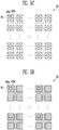
- FIGS. 5A to 5D are plan views of an arrangement of pixel circuits, pinholes and image sensors in accordance with an embodiment of the present disclosure.
- FIGS. 5A to 5D are plan views that illustrate the relative size, resolution and/or arrangement of the pixel circuits PC, the pinholes 120a, and the image sensors 160a, located in the sensing area SA of the display area DA shown in FIGS. 1A and 1B .
- the sensing area SA includes the pinholes 120a, of which there are fewer than there are pixel circuits PC, and the image sensors 160a, of which there are fewer than there are pixel circuits PC.
- the pinholes 120a and the image sensors 160a are smaller in size than the pixel circuits PC, and have a distribution density in the sensing area SA that is less than that of the pixel circuits PC.
- the density of the pinholes 120a and the image sensors 160a is not less than that of the pixel circuits PC.
- the number and spacing of pinholes 120a distributed in the sensing area SA is the same as those of the image sensors 160a distributed in the sensing area SA such that there is a one-to-one correspondence between the pinholes 120a and the image sensors 160a. In this case, the pinholes 120a and the image sensors 160a overlap each other.
- the pinholes 120a and the image sensors 160a have the same size. As one alternative, the pinhole 120a is larger than the image sensor 160a. As another alternative, the pinhole 120a is smaller than the image sensor 160a.
- the sensing area SA has fewer pinholes 120a than pixel circuits PC, but more image sensors 160a than pixel circuits PC.
- the pinholes 120a and the image sensors 160a are smaller in size than the pixel circuits PC.
- the pinholes 120a have a lower distribution density in the sensing area SA than the pixel circuits PC, and the image sensors 160a are compactly distributed in the sensing area SA with a higher density than pixel circuits PC.
- some of the image sensors 160a overlap the pinhole 120a and/or the pixel circuit PC.
- some of the image sensors 160a overlap the pinhole 120a and/or the pixel circuit PC, while other image sensors 160a are located in gaps between the pixel circuits PC.
- the image sensors 160a distributed in the sensing area SA have smaller sizes and higher density than the image sensors 160a illustrated in FIG. 5B .
- the image sensors 160a in the sensing area SA are separated by intervals that are about 1/10 to 1/100 times smaller than the spacing of the pinholes 120a.
- the image sensors 160a may be compactly distributed in the sensing area SA so that there is no longer a one-to-one correspondence between the image sensors 160a and the pixel circuits PC and/or the pinholes 120a. Therefore, a moiré phenomenon can be prevented or minimized regardless of arrangement of the image sensors 160a with respect to the pixel circuits PC and/or the pinholes 120a.
- the pinholes 120a have a distribution density in the sensing area SA that is equal to or different from that of the pixel circuits PC. As one example, as illustrated in FIG. 5C , the pinholes 120a have a distribution density in the sensing area SA that is the same as that of the pixel circuits PC. As another example, as illustrated in FIG. 5D , the pinholes 120a have a distribution density in the sensing area SA that is lower than that of the pixel circuits PC.
- the pinholes 120a and the image sensors 160a are regularly arranged in the sensing area SA.
- the pinholes 120a and/or the image sensors 160a can be irregularly distributed within the sensing area SA, or may have different densities in different areas of the sensing area SA.
- FIG. 6 is a sectional view of an electroluminescent device illustrated in FIG. 1A or FIG. 1B in accordance with an embodiment of the present disclosure. The description of components that are the same as or similar to those of the electroluminescent device described in FIG. 2 will be omitted herein.
- the pixel circuit structure 130 is used as a first light blocking structure 130 to selectively block or transmit reflected light RL reflected by a user's fingerprint.
- the first light blocking structure 130 includes pinholes 130a (hereinafter, also referred as effective pinholes 130a).
- a second light blocking structure 120 is located between the first light blocking structure 130 and the transparent layer 110.
- the first light blocking structure 130 has a plurality of pinholes 130a.
- the pinholes 130a of the first light blocking structure 130 overlap the pinholes 120a of the second light blocking structure 120.
- the pinholes 130a of the first light blocking structure 130 have the same size as the pinholes 120a of the second light blocking structure 120.
- the pinholes 130a of the first light blocking structure 130 differ in size from the pinholes 120a of the second light blocking structure 120.
- the pinholes 130a of the first light blocking structure 130 have a smaller width than the pinholes 120a of the second light blocking structure 120.
- the pinholes 130a of the first light blocking structure 130 and the pinholes 120a of the second light blocking structure 120 respectively have first and second widths in a range of 5 ⁇ m to 20 ⁇ m, where the second width is larger than the first width.
- a focus F is located at the pinhole 130a of the first light blocking structure 130.
- the pinholes 130a of the first light blocking structure 130 have a larger width than the pinholes 120a of the second light blocking structure 120.
- the pinholes 130a of the first light blocking structure 130 and the pinholes 120a of the second light blocking structure 120 respectively have first and second widths in a range of 5 ⁇ m to 20 ⁇ m, where the second width is smaller than the first width.
- the focus F is located at the pinhole 120a of the second light blocking structure 120.
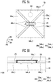
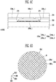
- FIG. 7 is a plan view of a touch sensing structure illustrated in FIG. 2
- FIG. 8A is an enlarged plan view of portion EA1 of FIG. 7
- FIG. 8B is a sectional view taken along line I-I' of FIG. 8A in accordance with an embodiment of the present disclosure
- FIG. 8C is a sectional view taken along line I-I' of FIG. 8A in accordance with an embodiment of the present disclosure
- FIG. 8D is an enlarged plan view of portion EA2 of FIG. 8A .
- the touch sensing structure 200 is located above the electroluminescent panel 100.
- an intermediate insulation layer may be located between the encapsulation structure 150 and the touch sensing structure 200.
- the touch sensing structure 200 includes the sensing area SA and the non-sensing area NSA that surrounds at least a part of the sensing area SA.
- the sensing area SA of the touch sensing structure 200 overlaps the display area DA of the electroluminescent panel 100.
- the touch sensing structure 200 includes a sensing electrode 220a that includes a first sensing electrode 220a_1 and a second sensing electrode 220a_2, and a bridge 240a that includes a first bridge 240a_1 and a second bridge 240a_2.
- the sensing electrode 220a and the bridge 240a are located in the sensing area SA of the touch sensing structure 200.
- the first sensing electrode 220a_1 and the first bridge 240a_1 are alternately connected in a first direction DR1, and the second sensing electrode 220a_2 and the second bridge 240a_2 are alternately connected in a second direction DR2.
- the first bridge 240a_1 and the second bridge 240a_2 intersect in plan view.
- the touch sensing structure 200 further includes a first insulation layer 230 and a second insulation layer 250 whose configurations will be described below with reference to FIGS. 8B and 8C .
- the first bridge 240a_1 extends in the first direction DR1 and connects two neighboring first sensing electrodes 220a_1 to each other.
- the first bridge 240a_1 extends in a third direction DR3 and connects two neighboring first sensing electrodes 220a_1 in the first direction DR1 to each other.
- the first bridge 240a_1 extends in a fourth direction DR4 and connects two neighboring first sensing electrodes 220a_1 in the first direction DR1 to each other.
- a first portion of the first bridge 240a_1 extends in the third direction DR3 and a second portion connected to the first portion extends in the fourth direction DR4 and connect two neighboring first sensing electrodes 220a_1 in the first direction DR1 to each other.
- the second bridge 240a_2 extends in the second direction DR2 and connects two neighboring second sensing electrodes 220a_2 in the second direction DR2 to each other.
- the second bridge 240a_2 extends in the third direction DR3 and connects two neighboring second sensing electrodes 220a_2 in the second direction DR2 to each other.
- the second bridge 240a_2 extends in the fourth direction DR4 and connects two neighboring second sensing electrodes 220a_2 in the second direction DR2 to each other.
- a first portion of the second bridge 240a_2 extends in the third direction DR3 and a second portion connected to the first portion extends in the fourth direction DR4 and connect two neighboring second sensing electrodes 220a_2 in the second direction DR2 to each other.
- the first bridge 240a_1 and the first sensing electrode 220a_1 are located at different layers.
- the first bridge 240a_1 is integrated with the first sensing electrode 220a_1.
- the second bridge 240a_2 is integrated with the second sensing electrode 220a_2.
- the second bridge 240a_2 and the second sensing electrode 220a_2 are located at different layers.
- the non-sensing area NSA of the touch sensing structure 200 overlaps the non-display area NDA of the electroluminescent panel 100.
- a pad area 260 that includes pads 260a and a peripheral wiring 220b that connects the sensing electrodes 220a and the pads 260a are located in the non-sensing area NSA of the touch sensing structure 200.
- the peripheral wiring 220b includes first peripheral wiring 220b_1 connected to the first sensing electrode 220a_1 and second peripheral wiring 220b_2 connected to the second sensing electrode 220a_2.
- the first sensing electrode 220a_1 includes a conductive fine line 280 and holes H.
- the conductive fine line 280 includes a first conductive fine line 280a and a second conductive fine line 280b.
- the first sensing electrode 220a_1 includes the first conductive fine line 280a extending parallel to the third direction DR3, and the second conductive fine line 280b extending parallel to the fourth direction DR4.
- the first conductive fine line 280a and the second conductive fine line 280b are integrated with each other. Since the first sensing electrode 220a_1 includes the first conductive fine line 280a and the second conductive fine line 280b, the first sensing electrode 220a_1 has a mesh structure with holes H formed by the crossings of the first conductive fine lines 280a and the second conductive fine lines 280b.
- an area where all of a lower electrode, such as 143 of FIG. 9A , a luminous layer, such as 145 of FIG. 9A , and an upper electrode, such as 147 of FIG. 9A , overlap each other without the intervention of the insulation layer to substantially emit light is defined as a luminous area.
- the hole H of the first sensing electrode 220a_1 overlaps the luminous area.
- the first sensing electrode 220a_1 includes a flexible opaque metal, it does not block light emitted from the luminous area.
- At least one of the second sensing electrode 220a_2, the first bridge 240a_1 and/or the second bridge 240a_2 has a mesh structure with holes H while including a flexible opaque metal, like the first sensing electrode 220a_1.
- the first sensing electrode 220a_1, the second sensing electrode 220a_2 and the second bridge 240a_2 are disposed on the encapsulation structure 150.
- the second sensing electrode 220a_2 is connected to the second bridge 240a_2 in the second direction DR2.
- the second sensing electrode 220a_2 is integrated with the second bridge 240a_2.
- the first insulation layer 230 that covers the first sensing electrode 220a_1, the second sensing electrode 220a_2 and the second bridge 240a_2 is disposed on the encapsulation structure 150.
- the first insulation layer 230 includes contact holes 270 that expose the first sensing electrode 220a_1.
- the first bridge 240a_1 is disposed on the first insulation layer 230 and fills the contact hole 270.
- the first bridge 240a_1 is connected to neighboring first sensing electrodes 220a_1.
- the second insulation layer 250 is disposed to cover the first bridge 240a_1 on the first insulation layer 230.
- the touch sensing structure 200 illustrated in FIG. 8B can be formed by directly performing deposition processes and etching processes on the encapsulation structure 150.
- a first metal layer is formed by performing a sputtering process on the encapsulation structure 150. Thereafter, the first sensing electrode 220a_1, the second sensing electrode 220a_2 and the second bridge 240a_2 are formed by performing an etching process on the first metal layer.
- a preliminary insulation layer that covers the first sensing electrode 220a_1, the second sensing electrode 220a_2 and the second bridge 240a_2 is formed through a chemical vapor deposition (CVD) process.
- CVD chemical vapor deposition
- the first insulation layer 230 with contact holes 270 that expose the first sensing electrode 220a_1 is formed by performing an etching process on the preliminary insulation layer.
- a second metal layer is formed by performing a sputtering process on the first insulation layer 230.
- the first bridge 240a_1 connected to the first sensing electrode 220a_1and filling the contact hole 270 is formed by performing an etching process on the second metal layer.
- the first bridge 240a_1 is placed on the encapsulation structure 150.
- the first bridge 240a_1 is placed directly on the encapsulation structure 150.
- the first insulation layer 230 that covers the first bridge 240a_1 is disposed on the encapsulation structure 150.
- the first insulation layer 230 includes contact holes 270 that expose the first bridge 240a_1.
- the first sensing electrode 220a_1 and the second bridge 240a_2 are disposed on the first insulation layer 230.
- the first sensing electrode 220a_1 fills the contact hole 270.
- the second bridge 240a_2 is disposed between neighboring first sensing electrodes 220a_1.
- the second insulation layer 250 is disposed on the first insulation layer 230 and covers the first sensing electrode 220a_1 and the second bridge 240a_2.
- the touch sensing structure 200 illustrated in FIG. 8C can be formed by performing deposition processes and etching processes directly on the encapsulation structure 150.
- a first metal layer is formed by performing a sputtering process directly on the encapsulation structure 150. Thereafter, the first bridge 240a_1 is formed by performing an etching process on the first metal layer.
- a preliminary insulation layer that covers the first bridge 240a_1 is formed by a CVD process.
- the first insulation layer 230 with contact holes 270 that expose the first bridge 240a_1 is formed by performing an etching process on the preliminary insulation layer.
- a second metal layer is formed by performing a sputtering process on the first insulation layer 230.
- the first sensing electrode 220a_1, the second sensing electrode 220a_2, and the second bridge 240a_2 are formed on the first insulation layer 230 by performing an etching process on the second metal layer.
- the second sensing electrode 220a_2 is connected to the second bridge 240a_2 in the second direction DR2.
- the second sensing electrode 220a_2 is integrated with the second bridge 240a_2.
- the first sensing electrode 220a_1 is connected to the first bridge 240a_1 by filling the contact hole 270.
- the touch sensing structure 200 includes a repeated arrangement of unit blocks UB, where each unit block UB includes portions of neighboring first sensing electrodes 220a_1 that are adjacent in the first direction DR1, the first bridges 240a_1 that connect the neighboring first sensing electrodes 220a_1, portions of neighboring second sensing electrodes 220a_2 that are adjacent in the second direction DR2, and the second bridges 240a_2 that connect the neighboring second sensing electrodes 220a_2.
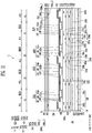
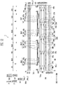
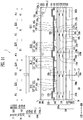
- FIG. 9A is a sectional view of an electroluminescent device shown in FIG. 6 in accordance with an embodiment of the present disclosure. To be more specific, FIG. 9A illustrates five pixels located in the sensing area of the electroluminescent device illustrated in FIGS. 1A and 1B . FIG. 9B is an enlarged sectional view of portion EA3 of FIG. 9A . FIG. 9C is an enlarged sectional view of portion EA4 of FIG. 9A .
- the electroluminescent device 1 includes the electroluminescent panel 100, the touch sensing structure 200, and the window 300.
- the electroluminescent panel 100 includes the luminous module 100a, the image sensor structure 160, and the protective layer 170.
- the luminous module 100a includes the transparent layer 110, the second light blocking structure 120, the insulation layer 131, the first light blocking structure 130, the electroluminescent structure 140, and the encapsulation structure 150.
- the touch sensing structure 200 has a structure described in FIG. 8B .
- the touch sensing structure 200 has a structure described in FIG. 8C .
- the luminous module 100a includes a pixel P.
- the pixel P includes the pixel circuit PC and the electroluminescent unit ELU electrically connected to the pixel circuit PC.
- the pixel circuit PC and the electroluminescent unit ELU do not overlap each other.
- at least a portion of the pixel circuit PC overlaps at least a portion of the electroluminescent unit ELU.
- the pixel P includes a first pixel P1, a second pixel P2, and a third pixel P3.
- the pixel circuit PC includes a first pixel circuit PC1, a second pixel circuit PC2, and a third pixel circuit PC3.
- the electroluminescent unit ELU includes the lower electrode 143, the luminous layer 145 disposed on the lower electrode 143, and the upper electrode 147 disposed on the luminous layer 145.
- the lower electrode 143 includes a first lower electrode 143a, a second lower electrode 143b, and a third lower electrode 143c.
- the luminous layer 145 includes a first luminous layer 145a, a second luminous layer 145b, and a third luminous layer 145c.
- the electroluminescent unit ELU can be defined in an area where the lower electrode 143 and the upper electrode 147 overlap each other.
- the electroluminescent unit ELU includes a first electroluminescent unit ELU1, a second electroluminescent unit ELU2, and a third electroluminescent unit ELU3.
- the first electroluminescent unit ELU1 includes a first lower electrode 143a, a first luminous layer 145a disposed on the first lower electrode 143a, and the upper electrode 147 disposed on the first luminous layer 145a.
- the second electroluminescent unit ELU2 includes a second lower electrode 143b, a second luminous layer 145b disposed on the second lower electrode 143b, and the upper electrode 147 disposed on the second luminous layer 145b.
- the third electroluminescent unit ELU3 includes a third lower electrode 143c, a third luminous layer 145c disposed on the third lower electrode 143c, and the upper electrode 147 disposed on the third luminous layer 145c.
- the first electroluminescent unit ELU1 and the first pixel circuit PC1 do not overlap each other.
- the first electroluminescent unit ELU1 overlaps the first pixel circuit PC1.
- the second electroluminescent unit ELU2 and the second pixel circuit PC2 do not overlap each other.
- the second electroluminescent unit ELU2 overlaps the second pixel circuit PC2.
- the third electroluminescent unit ELU3 and the third pixel circuit PC3 do not overlap each other.
- the third electroluminescent unit ELU3 overlaps the third pixel circuit PC3.
- the second light blocking structure 120 includes effective pinholes 120a and a light blocking area 120b.
- the second light blocking structure 120 selectively transmits the reflected light RL reflected by an object such as a user's finger on the first surface 1a of the electroluminescent device 1. Some of the reflected light RL incident on the second light blocking structure 120 is blocked by the light blocking area 120b, while at least a part of the remaining reflected light RL passes through the effective pinholes 120a to reach the image sensor structure 160 located under the second light blocking structure 120.
- the image sensor structure 160 includes effective image sensors 160a and dummy image sensors 160b, which are distributed at regular intervals to have a predetermined density.
- the effective image sensors 160a are used to sense an image on the first surface 1a, while the dummy image sensors 160b are not used to sense the image on the first surface 1a.
- the effective image sensor 160a has the same structure as the dummy image sensor 160b.
- an upper surface of the effective image sensor 160a senses an image
- an upper surface of the dummy image sensor 160b can likewise sense an image.
- upper and lower surfaces of the effective image sensor 160a can sense an image
- upper and lower surfaces of the dummy image sensor 160b can likewise sense an image.
- the effective image sensor 160a has a structure that differs from that of the dummy image sensor 160b.
- only the upper surface of the effective image sensor 160a can sense an image, while only the lower surface of the dummy image sensor 160b can sense an image.
- only the upper surface of the effective image sensor 160a can sense an image, but both the upper and lower surfaces of the dummy image sensor 160b can sense an image.
- both the upper and lower surfaces of the effective image sensor 160a can sense an image, but only the lower surface of the dummy image sensor 160b can sense an image.
- the effective image sensor 160a of the image sensor structure 160 is configured such that at least the upper surface can sense an image, and outputs as a sensing signal an electrical signal corresponding to the reflected light RL received by the upper surface through the effective pinholes 120a.
- the effective image sensor 160a overlaps the effective pinhole 120a of the second light blocking structure 120.
- the dummy image sensor 160b overlaps the light blocking area 120b of the second light blocking structure 120 without overlapping the effective pinhole 120a of the second light blocking structure 120.
- the insulation layer 131 is disposed on the second light blocking structure 120.
- the insulation layer 131 includes an inorganic insulator such as a silicon nitride, a silicon oxide or a silicon oxynitride to prevent impurities from the transparent layer 110 from penetrating into the electroluminescent unit ELU.
- the insulation layer 131 includes an organic insulating material.
- the insulation layer 131 may have a single-layered structure or a multi-layered structure.
- the first light blocking structure 130 is disposed on the insulation layer 131.
- the first light blocking structure 130 includes the effective pinholes 130a that contribute to sensing an image, and the dummy pinholes 130b that do not contribute to sensing an image.
- the first light blocking structure 130 includes at least one insulation layer and at least one conductive layer.
- the first light blocking structure 130 includes a first conductive pattern 137a and a first dummy conductive pattern 138a that are_located on the insulation layer 131, a gate insulation layer 132 that covers the first conductive pattern 137a and the first dummy conductive pattern 138a and is located on the insulation layer 131, a second conductive pattern 137b and a second dummy conductive pattern 138b that are located on the gate insulation layer 132, a first interlayer insulation layer 133 that covers the second conductive pattern 137b and the second dummy conductive pattern 138b and is located on the gate insulation layer 132, a third conductive pattern 137c and a third dummy conductive pattern 138c that are located on the first interlayer insulation layer 133, a second interlayer insulation layer 134 that covers the third conductive pattern 137c and the third dummy conductive pattern 138c and that is located on the first interlayer insulation layer 133, a fourth conductive pattern 137d and a fourth d
- the first conductive patterns 137a can be any one of a seventh source electrode SE7, a first drain electrode DE1, a 3b-th active pattern ACT3b, a 3b-th drain electrode DE3b, a 4b-th drain electrode DE4b, and a 4a-th drain electrode DE4a, which are shown in FIG. 23 .
- the second conductive patterns 137b can be any one of a i+1-th scan line Si+1, an i-th emission control line Ei, an i-th scan line Si, and an i-1-th scan line Si-1, which are shown in FIG. 23 .
- the third conductive patterns 137c can be any one of an initialization power line IPL and a capacitor upper electrode UE, which are shown in FIG. 23 .
- the fourth conductive patterns 137d can be any one of a pixel power line PL, a first connection line CNL1, and a second connection line CNL2, which are shown in FIG. 23 .
- the fifth conductive patterns 137e may be a connection pattern CNP shown in FIG. 23 .
- the first dummy conductive patterns 138a can be any one of a seventh source electrode SE7, a first drain electrode DE1, a 3b-th active pattern ACT3b, a 3b-th drain electrode DE3b, a 4b-th drain electrode DE4b, and a 4a-th drain electrode DE4a, which are shown in FIG. 23 .
- the second dummy conductive patterns 138b can be any one of a i+1-th scan line Si+1, an i-th emission control line Ei, an i-th scan line Si, and an i-1-th scan line Si-1, which are shown in FIG. 23 .
- the third dummy conductive patterns 138c can be any one of an initialization power line IPL and a capacitor upper electrode UE, which are shown in FIG. 23 .
- the fourth dummy conductive patterns 138d can be any one of a first connection line CNL1, a second connection line CNL2, and a pixel power line PL, which are shown in FIG. 23 .
- the fifth dummy conductive patterns 138e can be a connection pattern CNP shown in FIG. 23 .
- At least two of the first conductive pattern 137a, the second conductive pattern 137b, the third conductive pattern 137c, the fourth conductive pattern 137d, and the fifth conductive pattern 137e define the effective pinholes 130a of the first light blocking structure 130 in plan view.
- the effective pinholes 130a of the first light blocking structure 130 overlap the effective pinholes 120a of the second light blocking structure 120.
- At least two of the first dummy conductive pattern 138a, the second dummy conductive pattern 138b, the third dummy conductive pattern 138c, the fourth dummy conductive pattern 138d, and the fifth dummy conductive pattern 138e define the dummy pinholes 130b of the first light blocking structure 130 in plan view.
- the dummy pinholes 130b of the first light blocking structure 130 overlap the light blocking area 120b of the second light blocking structure 120 without overlapping the effective pinholes 120a of the second light blocking structure 120.
- the effective pinholes 130a of the first light blocking structure 130 may form a grid arrangement in plan view. Furthermore, the effective pinholes 130a and the dummy pinholes 130b of the first light blocking structure 130 may form a single grid arrangement in plan view.
- At least some of the reflected light RL propagates into an area between the effective pinholes 130a of the first light blocking structure 130, an area between the dummy pinholes 130b of the first light blocking structure 130, and an area between the effective pinholes 130a and the dummy pinholes 130b of the first light blocking structure 130.
- the at least some of the reflected light RL is blocked by the light blocking area 120b of the second light blocking structure 120.
- the fifth interlayer insulation layer 136 is disposed on the third interlayer insulation layer 135 and covers the fifth conductive patterns 137e and the fifth dummy conductive patterns 138e.
- the electroluminescent structure 140 includes a first electroluminescent unit ELU1, a second electroluminescent unit ELU2, and a third electroluminescent unit ELU3 and is disposed on the fifth interlayer insulation layer 136.
- the lower electrodes 143 are disposed on the fifth interlayer insulation layer 136.
- the lower electrodes 143 are reflective individual electrodes, while the upper electrode 147 is a transparent or translucent common electrode.
- the lower electrodes 143 are transparent or translucent individual electrodes, while the upper electrode 147 is a reflective common electrode.
- two neighboring lower electrodes 143 are spaced apart from each other by a third distance I_3. As illustrated in FIG. 9A , the first lower electrode 143a and the second lower electrode 143b are spaced apart from each other by the third distance I_3.
- the effective pinholes 130a of the first light blocking structure 130 are located in the second pixel circuit PC2, and do not overlap the lower electrode 143. To be more specific, the effective pinholes 130a of the first light blocking structure 130 do not overlap the second lower electrode 143b of the second electroluminescent unit ELU2.
- the dummy pinholes 130b of the first light blocking structure 130 are located in the third pixel circuit PC3, and do not overlap the lower electrode 143.
- the dummy pinholes 130b of the first light blocking structure 130 located in the third pixel circuit PC3 do not overlap the first, second and third lower electrodes 143a, 143b and 143c included in the first, second and third electroluminescent units ELU1, ELU2 and ELU3, respectively.
- the dummy pinholes 130b of the first light blocking structure 130 overlap the lower electrode 143.
- the lower electrode 143 blocks the reflected light RL incident on the dummy pinholes 130b of the first light blocking structure 130.
- the image sensor structure 160 can detect a relatively clear image.
- the optical center of the effective pinhole 130a located in the second pixel circuit PC2 of the second pixel P2 is spaced apart from the first lower electrode 143a in the fifth direction DR5 by a first distance D1
- the optical center of the effective pinhole 130a located in the second pixel circuit PC2 of the second pixel P2 is spaced apart from the second lower electrode 143b in the sixth direction DR6 by a third distance D3.
- the first distance D1 is equal to the third distance D3.
- the optical center of the effective pinhole 130a is a point where a vertical line passing through the focus F intersects a plane of a central portion of the effective pinhole 130a. If the focus F is formed in the effective pinhole 130a, the optical center of the effective pinhole 130a becomes the focus F.
- the optical center of the effective pinhole 130a is spaced apart from an inner wall ed of the effective pinhole 130a in the fifth direction DR5 by a second distance D2 and in the sixth direction DR6 by a fourth distance D4.
- the second distance D2 is equal to the fourth distance D4.
- the second distance D2 is less than the first distance D1.
- the fourth distance D4 is less than the third distance D3.
- the electroluminescent structure 140 includes a pixel defining layer 141 and spacers 142.
- the pixel defining layer 141 is disposed on the fifth interlayer insulation layer 136 and covers an edge of the lower electrode 143.
- the spacers 142 are disposed on the pixel defining layer 141.
- the spacers 142 are higher than the pixel defining layer 141.
- the upper surface of the spacer 142 is higher than the upper surface of the pixel defining layer 141.
- the spacer 142 includes a same material as the pixel defining layer 141, and is integrated with the pixel defining layer 141. Two neighboring spacers 142 are spaced apart from each other by a sixth distance I_6.
- the electroluminescent unit ELU further includes a first function layer 144 disposed between the lower electrode 143 and the luminous layer 145.
- the first function layer 144 is a common layer. In this case, the first function layer 144 is located above the lower electrode 143, the pixel defining layer 141 and the spacer 142.
- the first function layer 144 may be a hole injection layer (HIL), a hole transporting layer (HTL) or a multi-layered structure having a HIL and a HTL located on the HIL.
- HIL hole injection layer
- HTL hole transporting layer
- the luminous layer 145 is an individual layer.
- the luminous layer 145 may include an organic electroluminescent material or an inorganic electroluminescent material.
- the first luminous layer 145a, the second luminous layer 145b, and the third luminous layer 145c emit red, green and blue light, respectively.
- the first luminous layer 145a, the second luminous layer 145b, and the third luminous layer 145c emit magenta, cyan, and yellow light, respectively.
- At least two neighboring layers of the first luminous layer 145a, the second luminous layer 145b, and the third luminous layer 145c overlap a portion PT of the pixel defining layer 141 where no spacers 142 are located.
- the first luminous layer 145a and the second luminous layer 145b overlap a portion PT of the pixel defining layer 141 where no spacer 142 is located.
- An overlap area E of the first luminous layer 145a and the second luminous layer 145b overlaps the effective pinhole 130a of the first light blocking structure 130.
- the distance between the first electroluminescent unit ELU1, the second electroluminescent unit ELU2, and the third electroluminescent unit ELU3 is reduced to achieve a higher resolution and to reduce the scattering of reflected light RL by the spacer 142, thus obtaining a clearer fingerprint image.
- the electroluminescent unit ELU further includes a second function layer 146 disposed between the luminous layer 145 and the upper electrode 147.
- the second function layer 146 is a common layer.
- the second function layer 146 may be an electron injection layer (EIL), an electron transporting layer (ETL) or a multi-layered structure having an EIL and an ETL located on the EIL.
- the electroluminescent unit ELU includes the upper electrode 147 disposed on the second function layer 146.
- the upper electrode 147 is a cathode.
- the upper electrode 147 is a common electrode.
- the encapsulation structure 150 is disposed on the upper electrode 147 and covers the upper electrode 147.
- the encapsulation structure 150 includes a first inorganic layer, an organic layer on the first inorganic layer, and a second inorganic layer on the organic layer.
- the encapsulation structure 150 is a glass layer.
- the optical center of the effective pinhole 130a located in the second pixel circuit PC2 of the second pixel P2 is spaced apart from the spacer 142 in the fifth direction DR5 by a fifth distance D5 and in the sixth direction DR6 by a seventh distance D7.
- the fifth distance D5 is equal to the seventh distance D7.
- the fifth distance D5 is greater than the first distance D1.
- the seventh distance D7 is greater than the third distance D3.
- the spacers 142 are disposed on the pixel defining layer 141 without overlapping the effective pinholes 130a, so that a relatively clear fingerprint image can be obtained.
- the spacer 142 if the spacer 142 has a circular or curved edge when viewed in a plane and has a curved edge between upper and side surfaces when viewed in a cross-section, so that the spacer 142 serves as a condensing lens, the spacer 142 overlaps the effective pinholes 130a of the first light blocking structure 130. Since the spacer 142 serves as the condensing lens, the intensity of the reflected light RL is increased, so that it is possible to obtain a clearer fingerprint image. Furthermore, since no luminous material is applied to the upper surface of the spacer 142, it is possible to obtain a clearer fingerprint image.
- the bridge 240a of the touch sensing structure 200 does not overlap the effective pinhole 130a of the first light blocking structure 130.
- the reflected light RL incident on the effective pinhole 130a is absorbed or reflected to be diminished by the bridge 240a.
- the diminished reflected light RL reduces the sharpness of the fingerprint. Therefore, the bridge 240a is disposed to not overlap the effective pinhole 130a, thus preventing a reduction in the intensity of the reflected light RL incident on the effective pinhole 130a.
- two neighboring bridges 240a in a horizontal direction may be spaced apart from each other in the fifth direction DR5 by a seventh distance I_7.
- the seventh distance I_7 is greater than the sixth distance I_6.
- the optical center of the effective pinhole 130a of the first light blocking structure 130 located in the second pixel circuit PC2 of the second pixel P2 is spaced apart from the bridge 240a adjacent to the optical center in the fifth direction DR5 by a ninth distance D9 and in the sixth direction DR6 by an eleventh distance D11.
- the ninth distance D9 is equal to the eleventh distance D11.
- the ninth distance D9 is greater than the fifth distance D5.
- the eleventh distance D11 is greater than the seventh distance D7.
- the first light blocking structure 130 includes the dummy pinhole 130b.
- the dummy pinhole 130b overlaps the light blocking area 120b of the second light blocking structure 120.
- the dummy pinhole 130b overlaps the dummy image sensor 160b. Reflected light RL passing through the dummy pinhole 130b is blocked by the light blocking area 120b of the second light blocking structure 120. Therefore, the reflected light RL does not reach the dummy image sensor 160b.
- the size of the dummy pinhole 130b is equal to that of the effective pinhole 130a.
- the pixel circuit PC in which the effective pinhole 130a is formed and the pixel circuit PC in which the dummy pinhole 130b is located are equivalently designed, formation uniformity between the pixel circuits PC can be increased.
- the size of the dummy pinhole 130b is greater than that of the effective pinhole 130a.
- the dummy pinhole 130b is used as a passage to remove gas or impurities that may remain in the pixel circuit structure 130 after forming the pixel circuit structure 130 to reduce defects that can occur when the gas or the impurities are collected in one place.
- the size of the dummy pinhole 130b is larger than that of the effective pinhole 130a, the gas or the impurities can be more smoothly removed.
- the size of the dummy pinhole 130b is less than that of the effective pinhole 130a, or no dummy pinhole 130b is formed.
- Some reflected light RL passing through the dummy pinhole 130b may propagate to the effective pinhole 120a, and pass through the effective pinhole 120a. Thereby, this is detected as noise by the effective image sensor 160a. In this case, an unclear fingerprint image is obtained. Therefore, the size of the dummy pinhole 130b is less than that of the effective pinhole 130a, or no dummy pinhole 130b is formed, thus reducing noise.
- the dummy pinhole 130b may not overlap the spacer 142 and the bridge 240a. Alternatively, according to some embodiments, the dummy pinhole 130b overlaps at least one of the spacer 142 and/or the bridge 240a. In this case, reflected light RL incident on the dummy pinhole 130b can be reduced.
- an intermediate layer 180 is disposed on the image sensor structure 160.
- the intermediate layer 180 attaches the image sensor structure 160 to the transparent layer 110.
- the intermediate layer 180 is an optical clear adhesive (OCA).
- a predetermined voltage is applied to the light blocking area 120b of the second light blocking structure 120.
- the second light blocking structure 120 When the second light blocking structure 120 is in an electrically floating state, the voltage of the second light blocking structure 120 changes according to external influences, thus electrically unpredictably affecting the transistor and the capacitor in the pixel circuit PC.
- the second light blocking structure 120 has a ground state with one of a predetermined positive voltage, a predetermined negative voltage and a predetermined 0V. That is, the second light blocking structure 120 is electrically biased.
- the second light blocking structure 120 is connected to at least one electric conductor in the electroluminescent device 1 to be used as a static-electricity receiving member that discharges any static electricity accumulates in the electric conductor.
- a part of the inner wall ed of the effective pinhole 130a of the first light blocking structure 130 is defined by a part of an outer wall of the lower electrode 143.
- the part of the inner wall ed of the effective pinhole 130a of the first light blocking structure 130 and the part of the outer wall of the lower electrode 143 vertically correspond to each other. This will be described in detail with reference to FIG. 24 .
- FIG. 10 is a sectional view of an electroluminescent device shown in FIG. 6 in accordance with an embodiment of the present disclosure. The description of components that are already described in FIGS. 1A to 9C will be omitted herein.
- the second light blocking structure 120 has an additional pinhole 120c, and the first light blocking structure 130 includes a light blocking member 139 (hereinafter, also referred as a lower light blocking member 139).
- a light blocking member 139 hereinafter, also referred as a lower light blocking member 139.
- the additional pinhole 120c is used as a passage to remove gas or impurities to reduce defects that may occur when the gas or impurities are collected in one place. Furthermore, the additional pinhole 120c increase a surface area of the second light blocking structure 120 to increase an adhesive force between the insulation layer 131 and the second light blocking structure 120.
- the additional pinhole 120c is the same size as the effective pinhole 120a.
- the additional pinhole 120c is the same size as the effective pinhole 120a, holes of a mask used to form the first light blocking structure 130 can be uniformly formed, which simplifies a fabrication process.
- the additional pinhole 120c has a size that is greater than that of the effective pinhole 120a. In this case, the additional pinhole 120c can more effectively remove the gas or impurities.
- the additional pinhole 120c has a size that is less than that of the effective pinhole 120a.
- the additional pinhole 120c is smaller than the effective pinhole 120a, the intensity of the reflected light RL that passes through the additional pinhole 120c is diminished. Thus, noise generated by the reflected light RL passing through the additional pinhole 120c can be reduced.
- the additional pinhole 120c overlaps the lower electrode 143. Therefore, the lower electrode 143 reduces the intensity of the reflected light RL reflected towards the additional pinhole 120c.
- the additional pinhole 120c located in the first pixel P1 overlaps the first lower electrode 143a.
- the additional pinhole 120c located in the third pixel P3 overlaps the third lower electrode 143c.
- the first light blocking structure 130 includes the light blocking member 139.
- the light blocking member 139 overlaps the additional pinhole 120c and the first lower electrode 143a. Therefore, the light blocking member 139 reduces the intensity of the reflected light RL reflected towards the additional pinhole 120c. Thus, noise generated by the reflected light RL passing through the additional pinhole 120c can be reduced.
- the light blocking member 139 has a size greater than that of the additional pinhole 120c. Therefore, the light blocking member 139 effectively reduces the intensity of the reflected light RL incident on the additional pinhole 120c.
- the light shielding member 139 is disposed on at least one of a first layer on which the first conductive pattern 137a is disposed, a second layer on which the second conductive pattern 137b is disposed, a third layer on which the third conductive pattern 137c is disposed, a fourth layer on which the fourth conductive pattern 137d is disposed, and/or a fifth layer on which the fifth conductive pattern 137e is disposed.
- the light blocking member 139 has a single-layered structure.
- the light blocking member 139 has a multi-layered structure that includes a first light blocking layer, an insulation layer on the first light blocking layer, and a second light blocking layer on the insulation layer.
- the light blocking member 139 is located above the second light blocking structure 120.
- the light blocking member 139 is located under the second light blocking structure 120.
- the light blocking member 139 is located at least between the effective image sensor 160a and the additional pinhole 120c to block the reflected light RL that passes through the additional pinhole 120c from propagating towards the effective image sensor 160a.
- FIG. 11 is a sectional view of an electroluminescent device shown in FIG. 6 in accordance with an embodiment of the present disclosure. The description of components that are already described in FIGS. 1A to 10 will be omitted herein.
- a third light blocking structure 190 is located under the intermediate layer 180 and between the image sensor structure 160 and the protective layer 170.
- the third light blocking structure 190 prevents light incident on the second surface 1b of the electroluminescent device 1 from propagating towards the image sensor structure 160.
- the third light blocking structure 190 includes a light blocking material.
- the light blocking material may be a reflecting material or a light absorbing material.
- At least one intermediate layer may be located between the third light blocking structure 190 and the image sensor structure 160.
- the intermediate layer includes a transparent insulating material.
- FIG. 12 is a sectional view of an electroluminescent device shown in FIG. 6 in accordance with an embodiment of the present disclosure. The description of components that are already described in FIGS. 1A to 11 will be omitted herein.
- the third light blocking structure 190 has an effective pinhole 190a and a dummy pinhole 190b.
- the effective pinhole 190a overlaps the dummy image sensor 160b of the image sensor structure 160 and the spacer 142 on the pixel defining layer 141 of the electroluminescent structure 140, but does not overlap the effective image sensor 160a.
- the effective pinhole 190a is filled with a transparent insulation layer 190a_1.
- the transparent insulation layer 190a_1 includes an organic material.
- a portion of the light incident on the second surface 1b of the electroluminescent device 1 is blocked by the third light blocking structure 190, while a portion of the remaining light reaches the dummy image sensor 160b through the effective pinhole 190a.
- the lower surface is configured to perform a light sensing function, thus detecting a user's fingerprint, etc., on the second surface 1b.
- the dummy image sensors 160b function as a camera that photographs an object that is spaced apart from the second surface 1b.
- At least one intermediate layer is located between the third light blocking structure 190 and the image sensor structure 160.
- the intermediate layer includes a transparent insulating material.
- the transparent insulation layer 190a_1 is a part of the intermediate layer.
- the effective pinhole 190a is the same size as the dummy image sensor 160b, or is larger in size than the dummy image sensor 160b. In this case, it is possible to prevent a reduction of the intensity of light that passes through the effective pinhole 190a and is incident on the dummy image sensor 160b.
- the effective pinholes 190a are smaller in size than the dummy image sensor 160b. In this case, the intensity of noise light that passes through the effective pinhole 190a and, then, sensed by the effective image sensor 160a can be reduced.
- the dummy pinhole 190b of the third light blocking structure 190 is located between neighboring effective pinholes 190a. Gas or impurities remaining in the electroluminescent device 1 can be discharged from the electroluminescent device 1 through the dummy pinhole 190b of the third light blocking structure 190. Furthermore, the dummy pinhole 190b increases the surface area of the third light blocking structure 190 which increases an adhesive force between the intermediate layer 180 and the third light blocking structure 190.
- the dummy pinhole 190b does not overlap the effective image sensor 160a. Therefore, light passing through the dummy pinhole 190b from the second surface 1b is prevented from propagating to the effective image sensor 160a and acting as noise.
- the dummy pinhole 190b overlaps the effective image sensor 160a.
- the lower surface of the effective image sensor 160a is configured to not sense light. Therefore, a case where the light passing through the dummy pinhole 190b from the second surface 1b propagates to the effective image sensor 160a to act as noise can be minimized.
- the dummy pinhole 190b of the third light blocking structure 190 is smaller in size than the effective pinhole 190a. In this case, light incident through the dummy pinhole 190b can be prevented from propagating to the dummy image sensor 160b or the effective image sensor 160a and acting as noise.
- a light blocking member is located between the dummy pinhole 190b and the dummy image sensor 160b or between the dummy pinhole 190b and the effective image sensor 160a.
- the light blocking member prevents light passing through the dummy pinhole 190b from propagating to the dummy image sensor 160b or the effective image sensor 160a and acting as noise.
- FIG. 13 is a sectional view of an electroluminescent device shown in FIG. 6 in accordance with an embodiment of the present disclosure. The description of components that are already described in FIGS. 1A to 12 will be omitted herein.
- the sensing electrode 220a includes an opening 220c.
- a first sensing electrode 220a_1 includes an opening 220c.
- the opening 220c overlaps the effective pinhole 130a.
- one opening 220c vertically corresponds to the effective pinhole 130a and overlaps the effective pinhole 130a.
- at least two neighboring openings 220c vertically correspond to one effective pinhole 130a and overlap one effective pinhole 130a.
- a width of the opening 220c is equal to or greater than a width RLW of the reflected light RL measured by the sensing electrode 220a.
- the width of the opening 220c is greater than the width of the effective pinhole 130a. Therefore, it is possible to prevent the reflected light RL from being absorbed or reflected by the sensing electrode 220a, thus preventing reduction of the intensity of the reflected light RL.
- the bridge 240a when the bridge 240a is relatively large, the bridge 240a also includes an effective pinhole that overlaps the effective pinhole 130a. Therefore, it is possible to prevent the reflected light RL from being absorbed or reflected by the bridge 240a, thus preventing reduction of the intensity of the reflected light RL.
- the opening 220c is larger than the hole H of the sensing electrode 220a shown in FIG. 9A .
- the sensing electrode 220a includes both the hole H shown in FIG. 9A and the opening 220c shown in FIG. 13 .
- the bridge 240a also includes both the hole H shown in FIG. 9A and the opening 220c shown in FIG. 13 .
- FIG. 14 is a sectional view of an electroluminescent device shown in FIG. 6 in accordance with an embodiment of the present disclosure. The description of components that are already described in FIGS. 1A to 13 will be omitted herein.
- the electroluminescent device 1 includes fourth light blocking structures 148 located between the fifth interlayer insulation layer 136 and the pixel defining layer 141.
- the fourth light blocking structure 148 is disposed on the same layer as the lower electrode 143.
- the fourth light blocking structures 148 have island shapes that do not surround the lower electrode 143.
- the fourth light blocking structure 148 includes at least one of an effective pinhole 148a and/or a dummy pinhole 148b.
- the effective pinhole 148a of the fourth light blocking structure 148, the effective pinhole 130a of the first light blocking structure 130, the effective pinhole 120a of the second light blocking structure 120, and the effective image sensor 160a overlap each other. Therefore, the reflected light RL can sequentially pass through the effective pinhole 148a, the effective pinhole 130a, and the effective pinhole 120a to be incident on the effective image sensor 160a.
- the dummy pinhole 148b of the fourth light blocking structure 148, the dummy pinhole 130b of the first light blocking structure 130, the light blocking area 120b of the second light blocking structure 120, and the dummy image sensor 160b overlap each other. Therefore, after the reflected light RL sequentially passes through the dummy pinhole 148b and the dummy pinhole 130b, the reflected light RL may be blocked by the light blocking area 120b and is not incident on the dummy image sensor 160b.
- the dummy pinhole 148b of the fourth light blocking structure 148 overlaps the spacer 142 on the pixel defining layer 141 of the electroluminescent structure 140. Therefore, after the reflected light RL is absorbed or scattered by the spacer 142 and the intensity of the reflected light RL is reduced, the reflected light RL is incident on the dummy pinhole 148b.
- the dummy pinhole 148b of the fourth light blocking structure 148 has the same size as the effective pinhole 148a. In this case, holes of a mask used to form the fourth light blocking structure 148 can be uniformly formed, which simplifies a fabrication process.
- the dummy pinhole 148b of the fourth light blocking structure 148 is larger than the effective pinhole 148a.
- the dummy pinhole 148b is used as a passage to remove gas or impurities that remain in the electroluminescent device 1 to reduce defects that can occur when the gas or the impurities are collected in one place.
- the size of the dummy pinhole 130b is larger than that of the effective pinhole 148a, the gas or the impurities can be more effectively removed.
- the dummy pinhole 148b of the fourth light blocking structure 148 is smaller than the effective pinhole 148a. After the reflected light RL that passes through the dummy pinhole 148b passes through the dummy pinhole 130b, most of the reflected light RL is blocked by the second light blocking structure 120. However, some of the reflected light RL may propagate through the effective pinhole 120a of the second light blocking structure 120, thus acting as noise. Therefore, the dummy pinhole 148b of the fourth light blocking structure 148 can be formed smaller than the effective pinhole 148a to reduce noise.
- the fourth light blocking structure 148 is not electrically connected to the lower electrode 143.
- the fourth light blocking structure 148 is electrically floated.
- a positive voltage, a negative voltage or a zero voltage is constantly applied to the fourth light blocking structure 148. This can prevent the occurrence of cross talk due to voltage fluctuations of the fourth light blocking structure 148.
- the focus of the reflected light RL is on the effective pinhole 148a of the fourth light blocking structure 148.
- a ninth distance I_9 is greater than an eighth distance I_8, a seventh distance I_7 is greater than the ninth distance I_9, a fourth distance I_4 is greater than the eighth distance I_8, and a fifth distance I_5 is greater than the fourth distance I_4.
- the focus of the reflected light RL is on the effective pinhole 130a of the first light blocking structure 130.
- the eighth distance I_8 is greater than the fourth distance I_4
- the ninth distance I_9 is greater than the eighth distance I_8
- the seventh distance I_7 is greater larger than the ninth distance I_9
- the fifth distance I_5 is greater than the fourth distance I_4.
- the focus of the reflected light RL is on the effective pinhole 120a of the second light blocking structure 120.
- the fourth distance I_4 is greater than the fifth distance I_5
- the eighth distance I_8 is greater than the fourth distance I_4
- the ninth distance I_9 is greater than the eighth distance I_8, and the seventh distance I_7 is greater than the ninth distance I_9.
- an upper light blocking member is located above the dummy pinhole 148b of the fourth light blocking structure 148.
- the upper light blocking member prevents the reflected light RL from being incident on the dummy pinhole 148b.
- the upper light blocking member is wider than the dummy pinhole 148b.
- a lower light blocking member is located under the dummy pinhole 148b of the fourth light blocking structure 148.
- the lower light blocking member blocks the reflected light RL that has passes through the dummy pinhole 148b.
- the lower light blocking member is wider than the dummy pinhole 148b.
- the lower light blocking member includes at least a part of a light blocking layer in the first light blocking structure 130.
- the light blocking layer is a conductive layer.
- the light blocking layer includes an opaque metal.
- the light blocking layer is an insulation layer.
- the light blocking layer includes a black matrix material.
- the fourth light blocking structure 148 is in an electrically floating state, the voltage of the fourth light blocking structure 148 changes according to external influences, thus electrically unpredictably affecting the transistor and the capacitor in the pixel circuit PC.
- the fourth light blocking structure 148 has a ground state with one of a predetermined positive voltage, a predetermined negative voltage and a predetermined 0V. That is, the fourth light blocking structure 148 is electrically biased.
- the fourth light blocking structure 148 is electrically connected to the upper electrode 147.
- FIG. 15 is a sectional view of an electroluminescent device shown in FIG. 6 in accordance with an embodiment of the present disclosure. The description of components that are already described in FIGS. 1A to 14 will be omitted herein.
- the electroluminescent structure 140 includes the fourth light blocking structure 148 that has at least one of the effective pinhole 148a and/or the dummy pinhole 148b.
- the fourth light blocking structure 148 is integrated with the lower electrode 143.
- the fourth light blocking structure 148 with effective pinhole 148a in the second pixel circuit PC2 of the second pixel P2 is integrated with a second lower electrode 143b.
- the fourth light blocking structure 148 with dummy pinhole 148b in the third pixel circuit PC3 of the third pixel P3 is integrated with a third lower electrode 143c.
- the effective pinhole 148a and the dummy pinhole 148b shown in FIG. 15 are substantially the same as the effective pinhole 148a and the dummy pinhole 148b already described in FIG. 14 , a detailed description thereof will be omitted herein.
- the upper light blocking member and the lower light blocking member of FIG. 15 are substantially the same as the upper light blocking member and the lower light blocking member already described with respect to FIG. 14 , a detailed description thereof will be omitted herein.
- the relationships between the ninth distance I_9, the fourth distance I_4, the fifth distance I_5, the eighth distance I_8, and the seventh distance I_7 shown in FIG. 15 are substantially equal to the relationships between the ninth distance I_9, the fourth distance I_4, the fifth distance I_5, the eighth distance I_8, and the seventh distance I_7 that have been already described in FIG. 14 , the description thereof will be omitted herein.
- FIG. 16 is a sectional view of an electroluminescent device shown in FIG. 6 in accordance with an embodiment of the present disclosure. The description of components that are already described in FIGS. 1A to 15 will be omitted herein.
- the electroluminescent structure 140 includes the fourth light blocking structure 148 having at least one of the effective pinhole 148a and/or the dummy pinhole 148b.
- the fourth light blocking structure 148 with the effective pinhole 148a located in the second pixel circuit PC2 of the second pixel P2 is integrated with the first lower electrode 143a.
- the fourth light blocking structure 148 with the dummy pinhole 148b located in the third pixel circuit PC3 of the third pixel P3 is integrated with the second lower electrode 143b.
- the effective pinhole 148a and the dummy pinhole 148b shown in FIG. 16 are substantially the same as the effective pinhole 148a and the dummy pinhole 148b already described in FIG. 14 , a detailed description thereof will be omitted herein.
- the upper light blocking member and the lower light blocking member of FIG. 16 are substantially that same as the upper light blocking member and the lower light blocking member already described with respect to FIG. 14 , a detailed description thereof will be omitted herein.
- the relationships between the ninth distance I_9, the fourth distance I_4, the fifth distance I_5, the eighth distance I_8, and the seventh distance I_7 shown in FIG. 16 are substantially equal to the relationships between the ninth distance I_9, the fourth distance I_4, the fifth distance I_5, the eighth distance I_8, and the seventh distance I_7 that have been already described in FIG. 14 , a description thereof will be omitted herein.
- FIG. 17 is a sectional view of an electroluminescent device shown in FIG. 6 in accordance with an embodiment of the present disclosure.
- FIG. 18 is a plan view of an electroluminescent device shown in FIG. 17 in accordance with an embodiment of the present disclosure. The description of components already described in FIGS. 1A to 16 will be omitted herein.
- the electroluminescent device 1 includes the fourth light blocking structure 148 and a lower light blocking member 139.
- the fourth light blocking structure 148 has at least one of the effective pinhole 148a and/or the dummy pinhole 148b.
- the fourth light blocking structure 148 and the lower electrode 143 are disposed on the same layer.
- the fourth light blocking structure 148 and the lower electrode 143 include the same material, and are formed by the same process.
- the fourth light blocking structure 148 is spaced apart from the lower electrode 143.
- the fourth light blocking structure 148 has a mesh structure that surrounds the lower electrodes 143 in plan view.
- the fourth light blocking structure 148 includes an opaque material that can reflect or absorb light.
- the fourth light blocking structure 148 includes an opaque conductive material.
- the opaque conductive material includes a metal.
- the fourth light blocking structure 148 is connected to the upper electrode 147 through the contact hole CH that penetrates at least the pixel defining layer 141.
- the contact hole CH penetrates the pixel defining layer 141.
- the contact hole CH penetrates the pixel defining layer 141 and the spacer 142.
- a voltage drop of the upper electrode 147 can be reduced.
- the fourth light blocking structure 148 is in an electrically floating state without being electrically connected to the upper electrode 147, the voltage of the fourth light blocking structure 148 changes according to external influences, thus electrically unpredictably affecting the transistor and the capacitor in the pixel circuit PC.
- the fourth light blocking structure 148 if the fourth light blocking structure 148 is not electrically connected to the upper electrode 147, the fourth light blocking structure 148 has a ground state with one of a predetermined positive voltage, a predetermined negative voltage and a predetermined 0V. That is, if the fourth light blocking structure 148 is not electrically connected to the upper electrode 147, the fourth light blocking structure 148 is electrically biased.
- the effective pinhole 148a and the dummy pinhole 148b shown in FIG. 17 are substantially the same as the effective pinhole 148a and the dummy pinhole 148b that have been already described in FIG. 14 , a detailed description thereof will be omitted herein.
- the upper light blocking member is substantially that same as the upper light blocking member already described with respect to FIG. 14 , a detailed description thereof will be omitted herein.
- the lower light blocking member 139 is located under the dummy pinhole 148b of the fourth light blocking structure 148.
- the lower light blocking member 139 blocks the reflected light RL passing through the dummy pinhole 148b.
- the lower light blocking member 139 is wider than the dummy pinhole 148b.
- the lower light blocking member 139 includes at least a part of the light blocking layer in the first light blocking structure 130.
- the light blocking layer is a conductive layer.
- the light blocking layer includes the same material as the fifth conductive pattern 137e and the fifth dummy conductive pattern 138e disposed on the third interlayer insulation layer 135, and is formed in the same process.
- the light blocking layer is an insulation layer.
- the light blocking layer includes a black matrix material.
- the relationships between the ninth distance I_9, the fourth distance I_4, the fifth distance I_5, the eighth distance I_8, and the seventh distance I_7 shown in FIG. 17 are substantially equal to the relationships between the ninth distance I_9, the fourth distance I_4, the fifth distance I_5, the eighth distance I_8, and the seventh distance I_7 already described in FIG. 14 , a description thereof will be omitted herein.
- FIG. 19 is a plan view of a positional relationship between effective pinholes, lower electrodes, spacers and bridges in accordance with an embodiment of the present disclosure. At least one effective pinhole needs to satisfy conditions described with reference to FIG. 19 , but not all of the effective pinholes need to satisfy the conditions.
- an effective pinhole EPH has a square shape in plane.
- the effective pinhole EPH may have the shape of a rectangle, a circle, an ellipse, or a polygon in plane.
- a location where the focus F is formed becomes the effective pinhole EPH of FIG. 19 .
- multiple lower electrodes 143, multiple spacers 142, and multiple bridges 240a are located around the effective pinhole EPH in plan view.
- the lower electrodes 143 include a first lower electrode 143a, a second lower electrode 143b, and a third lower electrode 143c.
- the spacers 142 include a first spacer 142a and a second spacer 142b.
- the bridges 240a include a first bridge 240a_1 and a second bridge 240a_2.
- the multiple lower electrodes 143 include a single first lower electrode 143a that is firstly closest in plan view to the focus F formed on the effective pinhole EPH.
- the shortest distance between the single first lower electrode 143a and the focus F is a first distance D1 that is the length of a first line L1.
- the focus F is spaced apart from the inner wall ed of the effective pinhole EPH by a second distance D2 in an extension direction of the first line L1.
- the first distance D1 is equal to or greater than the second distance D2.
- the first distance D1 is greater than the second distance D2.
- the multiple lower electrodes 143 include a single second lower electrode 143b that is secondly closest in plan view to the focus F formed on the effective pinhole EPH.
- the multiple lower electrodes 143 include at least two second lower electrodes 143b that are secondly closest in plan view to the focus F.
- the shortest distance between the second lower electrode 143b and the focus F is a third distance D3 that is the length of a second line L2.
- the focus F is spaced apart from the inner wall ed of the effective pinhole EPH by a fourth distance D4 in an extension direction of the second line L2.
- the third distance D3 is equal to or greater than the fourth distance D4.
- the third distance D3 is greater than the fourth distance D4.
- the multiple spacers 142 include a single first spacer 142a that is firstly closest in plan view to the focus F formed on the effective pinhole EPH.
- the shortest distance between the single first spacer 142a and the focus F is a fifth distance D5 that is the length of a third line L3.
- the focus F is spaced apart from the inner wall ed of the effective pinhole EPH by a sixth distance D6 in an extension direction of the third line L3.
- the fifth distance D5 is equal to or greater than the sixth distance D6.
- the fifth distance D5 is greater than the sixth distance D6.
- the multiple spacers 142 include a single second spacer 142b that is secondly closest in plan view to the focus F formed on the effective pinhole EPH.
- the multiple spacers 142 include at least two second spacers 142b that are secondly closest in plan view to the focus F formed on the effective pinhole EPH.
- the shortest distance between the second spacer 142b and the focus F is a seventh distance D7 that is the length of a fourth line L4.
- the focus F is spaced apart from the inner wall ed of the effective pinhole EPH by an eighth distance D8 in an extension direction of the fourth line L4.
- the seventh distance D7 is equal to or greater than the eighth distance D8.
- the seventh distance D7 is greater than the eighth distance D8.
- the multiple bridges 240a include a single first bridge 240a_1 that is firstly closest in plan view to the focus F formed on the effective pinhole EPH.
- the shortest distance between the single first bridge 240a_1 and the focus F is a ninth distance D9 that is the length of the fifth line L5.
- the focus F is spaced apart from the inner wall ed of the effective pinhole EPH by a tenth distance D10 in an extension direction of the fifth line L5.
- the ninth distance D9 is equal to or greater than the tenth distance D10.
- the ninth distance D9 is greater than the tenth distance D10.
- the first bridge 240a_1 has an overlap area a_1 that overlaps the first sensing electrode 220a_1 illustrated in FIG. 8A , and the light transmissivity of the touch sensing structure 200 is lower at the overlap area a_1. Therefore, the fifth line L5 may be set between the focus F and the overlap area a_1 of the single first bridge 240a_1 that is firstly closest in plane to the focus F.
- the multiple bridges 240a include a single second bridge 240a_2 that is secondly closest in plan view to the focus F formed on the effective pinhole EPH.
- the multiple bridges 240a include at least two second bridges 240a_2 that are secondly closest in plan view to the focus F formed on the effective pinhole EPH.
- the shortest distance between the focus F and the second bridge 240a_2 that is secondly closest in plane to the focus F is an eleventh distance D11 that is the length of a sixth line L6.
- the focus F is spaced apart from the inner wall ed of the effective pinhole EPH by a twelfth distance D12 in an extension direction of the sixth line L6.
- the eleventh distance D11 is equal to or greater than the twelfth distance D12.
- the eleventh distance D11 is greater than the twelfth distance D12.
- the second bridge 240a_2 has an overlap area a_2 that overlaps the second sensing electrode 220a_2 illustrated in FIG. 8A , and the light transmissivity of the touch sensing structure 200 is lower at the overlap area a_2. Therefore, the sixth line L6 may be set between the focus F and the overlap area a_2 of the single second bridge 240a_2 that is secondly closest in plane to the focus F.
- the first distance D1, the third distance D3, the fifth distance D5, the seventh distance D7, the ninth distance D9, and the eleventh distance D11 are equal to or greater than the second distance D2, the fourth distance D4, the sixth distance D6, the eighth distance D8, the tenth distance D10, and the twelfth distance D12, respectively. Therefore, at least a part of an optical path along which the reflected light RL propagates is blocked to prevent an intensity reduction of the reflected light RL.
- the third distance D3 is equal to or greater than the first distance D1.
- the fifth distance D5 is equal to or greater than the third distance D3.
- the seventh distance D7 is equal to or greater than the fifth distance D5.
- the ninth distance D9 is equal to or greater than the seventh distance D7.
- the eleventh distance D11 is equal to or greater than the ninth distance D9. Therefore, the optical path of the reflected light RL can be sufficiently secured. Therefore, at least a part of an optical path along which the reflected light RL propagates can be blocked to prevent an intensity reduction of the reflected light RL.
- a sum of the fifth distance D5 and the seventh distance D7 is equal to or greater than a sum of the first distance D1 and the third distance D3.
- a sum of the ninth distance D9 and the eleventh distance D11 is equal to or greater than the sum of the fifth distance D5 and the seventh distance D7. Therefore, at least a part of an optical path along which the reflected light RL propagates can be blocked to prevent an intensity reduction of the reflected light RL.
- a first angle ⁇ 1 between the first line L1 and the second line L2 is not 'k ⁇ 180°'.
- 'k' is an integer other than zero.
- a second angle ⁇ 2 between the third line L3 and the fourth line L4 is not 'm ⁇ 180°'.
- 'm' is an integer other than zero.
- a third angle ⁇ 3 between the fifth line L5 and the sixth line L6 is not 'n ⁇ 180°'.
- 'n' is an integer other than zero.
- At least one of the conditions of the first angle ⁇ 1, the conditions of the second angle ⁇ 2, and/or the conditions of the third angle ⁇ 3 can be satisfied. Therefore, the formation of the effective pinhole EPH does not prevent the resolution of the electroluminescent device 1 from increasing.
- FIG. 20 is a plan view is the positional relationship between the effective pinholes, the lower electrodes, the spacers and the bridges in accordance with an embodiment of the present disclosure. A description of components that have been already described in FIG. 19 will be omitted herein. At least one effective pinhole needs to satisfy the conditions described with reference to FIG. 20 , but not all of the effective pinholes need to satisfy the conditions.
- the electroluminescent device 1 includes at least two lower electrodes 143 that are firstly closest in plan view to the focus F formed on the effective pinhole EPH.
- the shortest distance between the focus F and the at least two lower electrodes 143 is a 13-th distance D13.
- the 13-th distance D13 may correspond the first distance D1 or the third distance D3 illustrated in FIG. 19 .
- the electroluminescent device 1 includes at least two spacers 142 that are firstly closest in plan view to the focus F formed on the effective pinhole EPH.
- the shortest distance between the focus F and the at least two spacers 142 is a 14-th distance D14.
- the 14-th distance D14 may correspond the fifth distance D5 or the seventh distance D7 illustrated in FIG. 19 .
- the electroluminescent device 1 includes at least two bridges 240a that are firstly closest in plan view to the focus F formed on the effective pinhole EPH.
- the shortest distance between the focus F and the at least two bridges 240a is a 15-th distance D15.
- the 15-th distance D15 may correspond the ninth distance D9 or the eleventh distance D11 illustrated in FIG. 19 .
- the bridge 240a has an overlap area a that overlaps the sensing electrode 220a illustrated in FIG. 8A , and the light transmissivity of the touch sensing structure 200 is lower at the overlap area a. Therefore, the 15-th distance D15 may be set between the focus F and the overlap areas a of at least two bridges 240a that are firstly closest to the focus F.
- the 14-th distance D14 is equal to or greater than the 13-th distance D13.
- the 15-th distance D15 is equal to or greater than the 14-th distance D14. Therefore, the optical path of the reflected light RL can be sufficiently secured. Therefore, an intensity reduction of the reflected light RL may be prevented.
- the intensity reduction of the reflected light RL may be caused by blocking at least a part of an optical path along which the reflected light RL propagates.
- the distance between the focus F formed on the effective pinhole EPH and the inner wall ed of the effective pinhole EPH is length R1.
- FIG. 21 is a circuit diagram of a pixel circuit shown in FIG. 1A or FIG. 1B in accordance with an embodiment of the present disclosure.
- the pixel Pij is arranged in an i-th, row, where 'i' is a natural number, and a j-th column, where 'j' is a natural number, of the display area DA of the electroluminescent device 1.
- the pixel circuit PCij of the pixel Pij is coupled to an i-th scan line Si and a j-th data line Dj of the display area DA.
- the pixel circuit PCij is coupled to a first pixel power supply ELVDD and a second pixel power supply ELVSS.
- the pixel Pij includes the pixel circuit PCij and the electroluminescent unit ELUij.
- the pixel circuit PCij is electrically coupled to the electroluminescent unit ELUij.
- An outer portion of the pixel circuit PCij substantially has the shape of a tetragon, such as a square or a rectangle.
- the pixel circuit PCij is further coupled to at least one different scan line.
- the pixel circuit PCij is further coupled to at least one of an i-1-th scan line Si-1 and/or an i+1-th scan line Si+1.
- the pixel circuit PCij is further coupled to a third power supply in addition to the first pixel power supply ELVDD and the second pixel power supply ELVSS.
- the pixel circuit PCij is also coupled to an initialization power supply Vint.
- the pixel circuit PCij includes first to seventh transistors T1, T2, T3, T4, T5, T6 and T7 and a storage capacitor Cst.
- a source electrode of the first transistor T1 is coupled to the first pixel power supply ELVDD via the fifth transistor T5.
- a drain electrode of the first transistor T1 is coupled to the electroluminescent unit ELUij via the sixth transistor T6.
- a gate electrode of the first transistor T1 is coupled to a first node N1.
- the first transistor T1 controls a driving current that flows between the first pixel power supply ELVDD and the second pixel power supply ELVSS so that the driving current flows through the electroluminescent unit ELUij in response to the voltage of the first node N1.
- the second transistor T2 is coupled between a j-th data line Dj and the source electrode of the first transistor T1.
- the gate electrode of the second transistor T2 is coupled to the i-th scan line Si.
- the scan signal of the gate-on voltage such as a low voltage
- the second transistor T2 turns on to electrically connect the j-th data line Dj to the source electrode of the first transistor T1.
- a data signal received from the j-th data line Dj is transmitted to the first transistor T1.
- the third transistor T3 is coupled between the drain electrode of the first transistor T1 and the first node N1.
- the gate electrode of the third transistor T3 is coupled to the i-th scan line Si.
- the third transistor T3 turns on to electrically connect the drain electrode of the first transistor T1 to the first node N1.
- the fourth transistor T4 is coupled between the first node N1 and the initialization power line IPL over which the initialization power supply Vint is transmitted.
- the gate electrode of the fourth transistor T4 is coupled to a preceding scan line, such as the i-1-th scan line Si-1.
- the fourth transistor T4 turns on so that the voltage of the initialization power supply Vint flows to the first node N1.
- the initialization power supply Vint has a voltage that is equal to or less than a minimum voltage of the data signal.
- the fifth transistor T5 is coupled between the first pixel power supply ELVDD and the first transistor T1.
- the gate electrode of the fifth transistor T5 is coupled to a corresponding emission control line, such as an i-th emission control line Ei.
- the fifth transistor T5 turns off when an emission control signal having a gate-off voltage is received by the i-th emission control line Ei, and can be turned on in other cases.
- the sixth transistor T6 is coupled between the first transistor T1 and the electroluminescent unit ELUij.
- the gate electrode of the sixth transistor T6 is coupled to the i-th emission control line Ei.
- the sixth transistor T6 turns off when an emission control signal having a gate-off voltage is supplied to the i-th emission control line Ei, and may be turned on in other cases.
- the seventh transistor T7 is coupled between the electroluminescent unit ELUij and the initialization power line IPL.
- the gate electrode of the seventh transistor T7 is coupled to any one of scan lines of a subsequent stage, such as the i+1-th scan line Si+1.
- the seventh transistor T7 turns on so that the voltage of the initialization power supply Vint flows to the electroluminescent unit ELUij.
- the storage capacitor Cst is coupled between the first pixel power supply ELVDD and the first node N1.
- the storage capacitor Cst stores a voltage that corresponds to the data signal supplied to the first node N1 during each frame period and to the threshold voltage of the first transistor T1.
- an anode of the electroluminescent unit ELUij is coupled to the first transistor T1 via the sixth transistor T6, and a cathode of the electroluminescent unit ELUij is coupled to the second pixel power supply ELVSS.
- the electroluminescent unit ELUij emits light having a predetermined luminance that corresponds to current received from the first transistor T1.
- the voltage of the first pixel power supply ELVDD to be transmitted to the pixel power line PL is higher than that of the second pixel power supply ELVSS to allow current to flow to the electroluminescent unit ELUij.
- a potential difference between the first pixel power supply ELVDD and the second pixel power supply ELVSS is equal to or higher than a threshold voltage of the electroluminescent unit ELUij for the light emitting period of the pixel Pij.
- FIG. 22 is a plan view of a pixel shown in FIG. 21 in accordance with an embodiment of the present disclosure.
- FIG. 23 is a sectional view taken along line II-II' of FIG. 22 .
- an i-1-th row of the scan lines is referred to as an "i-1-th scan line Si-1
- an i-th row of the scan lines is referred to as an "i-th scan line Si”
- an i+1-th row of the scan lines is referred to as an "i+1-th scan line Si+1”.
- An i-th row of the emission control lines over which an emission control signal is transmitted is referred to as an "i-th emission control line Ei”.
- a j-th column of the data lines over which a data signal is transmitted is referred to as a "j-th data line Dj".
- a j-th column of the pixel power lines over which the first pixel power supply ELVDD is transmitted is referred to as a "pixel power line PL".
- the pixel Pij is disposed on the transparent layer 110.
- the electroluminescent device 1 includes a display area DA and a non-display area NDA.
- the pixel Pij is disposed in the display area DA.
- the scan lines Si-1, Si and Si+1 transmit the scan signal to the pixel circuit PCij.
- the i-th emission control line Ei transmits the emission control signal to the pixel circuit PCij.
- the j-th data line Dj transmits the data signal to the pixel circuit PCij.
- the initialization power line IPL transmits the initialization power to the pixel circuit PCij.
- the pixel power line PL transmits the first pixel power supply ELVDD to the pixel circuit PCij.
- the scan lines Si-1, Si and Si+1 extend in the first direction DR1 on the transparent layer 110.
- the scan lines Si-1, Si, and Si+1 are sequentially arranged in the second direction DR2.
- Each of the scan lines Si-1, Si, and Si+1 receive a scan signal.
- the scan lines Si-1, Si, and Si+1 are disposed on the gate insulation layer 132.
- the i-th emission control line Ei extends in the first direction DR1 on the transparent layer 110.
- the i-th emission control line Ei is disposed on the gate insulation layer 132.
- the j-th data line Dj extends on the transparent layer 110 in the second direction DR2 that intersecting with the first direction DR1.
- the j-th data line Dj receives a data signal.
- the j-th data line Dj is disposed on the second interlayer insulation layer 134.
- the pixel power line PL substantially extends in the same direction as the j-th data line Dj, which is the second direction DR2, on the transparent layer 110.
- the first pixel power supply ELVDD is transmitted over the pixel power line PL.
- the pixel power line PL is disposed on the second interlayer insulation layer 134.
- the initialization power line IPL extends in the first direction DR1 on the transparent layer 110.
- the initialization power supply Vint is transmitted over the initialization power line IPL.
- the initialization power line IPL is disposed on the first interlayer insulation layer 133.
- the pixel Pij includes an electroluminescent structure 140 that includes at least one electroluminescent unit ELUij, a pixel circuit structure 130 that includes a pixel circuit PCij that drives the electroluminescent unit ELUij, and a second light blocking structure 120 located between the pixel circuit structure 130 and the transparent layer 110.
- the pixel circuit structure 130 includes the effective pinholes 130a. Therefore, the pixel circuit structure 130 is used as the first light blocking structure 130 to selectively transmit the reflected light RL reflected by a user.
- the pixel circuit structure 130 is referred to as the first light blocking structure 130.
- the second light blocking structure 120 is disposed between the electroluminescent structure 140 and the image sensor structure 160 to selectively transmit the incident reflected light RL.
- the second light blocking structure 120 includes effective pinholes 120a and a light blocking area 120b.
- the light blocking area 120b includes a light blocking material.
- the light blocking area 120b includes an opaque metal.
- the first light blocking structure 130 includes the pixel circuit PCij coupled to the electroluminescent unit ELUij.
- the pixel circuit PCij includes first to seventh transistors T1, T2, T3, T4, T5, T6 and T7 and the storage capacitor Cst.
- the pixel circuit PCij is disposed on the insulation layer 131.
- the first transistor T1 includes a first gate electrode GE1, a first active pattern ACT1, a first source electrode SE1, a first drain electrode DE1, and a first connection line CNL1.
- the first gate electrode GE1 is coupled to a 3b-th drain electrode DE3b of a 3b-th transistor T3b and a 4b-th drain electrode DE4b of a 4b-th transistor T4b.
- the second transistor T2 includes a second gate electrode GE2, a second active pattern ACT2, a second source electrode SE2, and a second drain electrode DE2.
- the third transistor T3 has a double gate structure to prevent current leakage.
- the third transistor T3 includes a 3a-th transistor T3a and a 3b-th transistor T3b.
- the 3a-th transistor T3a includes a 3a-th gate electrode GE3a, a 3a-th active pattern ACT3a, a 3a-th source electrode SE3a, and a 3a-th drain electrode DE3a.
- the 3b-th transistor T3b includes a 3b-th gate electrode GE3b, a 3b-th active pattern ACT3b, a 3b-th source electrode SE3b, and a 3b-th drain electrode DE3b.
- the other end of the 3b-th drain electrode DE3b is coupled to the first gate electrode GE1 by the first and second contact holes CH1 and CH2 and the first connection line CNL1.
- the fourth transistor T4 has a double gate structure to prevent current leakage, similar to the third transistor T3.
- the fourth transistor T4 includes a 4a-th transistor T4a and a 4b-th transistor T4b.
- the 4a-th transistor T4a includes a 4a-th gate electrode GE4a, a 4a-th active pattern ACT4a, a 4a-th source electrode SE4a, and a 4a-th drain electrode DE4a.
- the 4b-th transistor T4b includes a 4b-th gate electrode GE4b, a 4b-th active pattern ACT4b, a 4b-th source electrode SE4b, and a 4b-th drain electrode DE4b.
- the 4a-th source electrode SE4a is coupled to an auxiliary connection line AUX through a ninth contact hole CH9.
- the 4b-th drain electrode DE4b is coupled to the first gate electrode GE1 of the first transistor T1 through the first and second contact holes CH1 and CH2 and the first connection line CNL1.
- the fifth transistor T5 includes a fifth gate electrode GE5, a fifth active pattern ACT5, a fifth source electrode SE5, and a fifth drain electrode DE5.
- the fifth source electrode SE5 is coupled to the pixel power line PL through a fifth contact hole CH5.
- the sixth transistor T6 includes a sixth gate electrode GE6, a sixth active pattern ACT6, a sixth source electrode SE6, and a sixth drain electrode DE6.
- the sixth source electrode SE6 is coupled to the first drain electrode DE1 and the 3a-th source electrode SE3a.
- the sixth drain electrode DE6 is coupled to a second connection line CNL2 through a seventh contact hole CH7.
- the second connection line CNL2 is coupled to a connection pattern CNP through a tenth contact hole CH10.
- connection pattern CNP is coupled to the second connection line CNL2 through the tenth contact hole CH10 that penetrates the third interlayer insulation layer 135, and is coupled to the lower electrode 143 of the electroluminescent structure 140 through the eleventh contact hole CH11 that penetrates the fifth interlayer insulation layer 136.
- the seventh transistor T7 includes a seventh gate electrode GE7, a seventh active pattern ACT7, a seventh source electrode SE7, and a seventh drain electrode DE7.
- the seventh source electrode SE7 is coupled to the sixth drain electrode DE6, and the seventh drain electrode DE7 is coupled to the initialization power line IPL through an eighth contact hole CH8 and is coupled to the 4a-th source electrode SE4a of a pixel P(i+1)j corresponding the i+1-th row of the scan lines.
- the storage capacitor Cst includes a capacitor lower electrode LE and a capacitor upper electrode UE.
- the capacitor lower electrode LE is integrated with the first gate electrode GE1 of the first transistor T1.
- the capacitor upper electrode UE overlaps the capacitor lower electrode LE, and covers the capacitor lower electrode LE when viewed from a plane.
- the capacitor upper electrode UE is electrically connected to the pixel power line PL through third and fourth contact holes CH3 and CH4.
- the capacitor upper electrode UE includes an opening OPN that corresponds to an area in which the first contact hole CH1 is formed.
- the first gate electrode GE1 of the first transistor T1 is coupled with the first connection line CNL1 through the first contact hole CH1.
- the electroluminescent unit ELUij includes the lower electrode 143, the upper electrode 147, and the luminous layer 145 disposed between the lower electrode 143 and the upper electrode 147. All of the lower electrode 143, the luminous layer 145 and the upper electrode 147 overlap each other without the intervention of an insulation layer, so that an area where light is actually emitted is the luminous area.
- the first light blocking structure 130 of the sensing area SA has effective pinholes 130a that overlap the effective pinholes 120a of the second light blocking structure 120.
- the focus F of the reflected light RL is located on the effective pinhole 130a of the first light blocking structure 130.
- the size of the effective pinholes 130a of the first light blocking structure 130 is smaller than that of the effective pinholes 120a of the second light blocking structure 120.
- the focus F of the reflected light RL is located on the effective pinhole 120a of the second light blocking structure 120. In this case, the size of the effective pinholes 120a of the second light blocking structure 120 is smaller than that of the effective pinholes 130a of the first light blocking structure 130.
- the effective pinhole 130a of the first light blocking structure 130 is defined by at least two of the first to fifth conductive patterns 137a, 137b, 137c, 137d, and 137e.
- the first conductive pattern 137a is one of a seventh source electrode SE7, a first drain electrode DE1, a 3b-th active pattern ACT3b, a 3b-th drain electrode DE3b, a 4b-th drain electrode DE4b, and a 4a-th drain electrode DE4a, which are shown in FIG. 23 .
- the second conductive pattern 137b is one of a i+1-th scan line Si+1, an i-th emission control line Ei, an i-th scan line Si, and an i-1-th scan line Si-1, which are shown in FIG. 23 .
- the third conductive pattern 137c is one of an initialization power line IPL and a capacitor upper electrode UE, which are shown in FIG.
- the fourth conductive pattern 137d is one of a pixel power line PL, a first connection line CNL1, and a second connection line CNL2, which are shown in FIG. 23 .
- the fifth conductive pattern 137e is a connection pattern CNP shown in FIG. 23 .
- the electroluminescent device 1 further includes the touch sensing structure 200 disposed on the electroluminescent structure 140. Since the touch sensing structure 200 has been described in FIGS. 7 and 8D , a duplicate description thereof will be omitted herein.
- FIG. 24 is a plan view of a pixel shown in FIG. 21 in accordance with an embodiment of the present disclosure.
- the effective pinholes 130a of the first light blocking structure 130 shown in FIG. 24 are defined by the j-th data line Dj, the pixel power line PL, the i-th emission control line Ei, and the lower electrode 143.
- a part of the inner wall of the effective pinhole 130a of the first light blocking structure 130 is defined by a part of an outer wall of the lower electrode 143.
- the part of the inner wall of the effective pinhole 130a of the first light blocking structure 130 and the part of the outer wall of the lower electrode 143 vertically correspond to each other.
- the lower electrode 143 is also included in the first light blocking structure 130.
- an electroluminescent device (1) comprising: a first insulation layer (136); an electroluminescent structure (140) including lower electrodes (143, 143a, 143b, 143c) disposed on the first insulation layer (136), luminous layers (145, 145a, 145b, 145c) disposed on the lower electrodes (143, 143a, 143b, 143c), and an upper electrode (147) disposed on the luminous layers (145, 145a, 145b, 145c); a first light blocking structure (130) disposed under the first insulation layer (136) and including first effective pinholes (130a); and an image sensor structure (160) disposed under the first light blocking structure (130) and including effective image sensors (160a) that overlap the first effective pinholes (130a).
- the lower electrodes (143, 143a, 143b, 143c) may not overlap the first effective pinholes (130a).
- the first light blocking structure (130) may further includes first dummy pinholes (130b), the first dummy pinhole (130b) may be located between the first effective pinholes (130a), and the first effective pinholes (130a) and the first dummy pinholes (130b) together may form a single grid arrangement in plan view.
- Embodiments may provide an electroluminescent device (1), comprising: an electroluminescent structure (140) including lower electrodes (143, 143a, 143b, 143c) disposed on an insulation layer (136), luminous layers (145, 145a, 145b, 145c) disposed on the lower electrodes (143, 143a, 143b, 143c), and an upper electrode (147) disposed on the luminous layers (145, 145a, 145b, 145c); a first light blocking structure (148) located on a same layer as the lower electrodes (143, 143a, 143b, 143c); and an image sensor structure (160) located under the insulation layer (136) and including effective image sensors (160a).
- the electroluminescent structure (140) may include luminous areas where the lower electrodes (143, 143a, 143b, 143c), the luminous layers (145, 145a, 145b, 145c) and the upper electrode (147) overlap each other to emit light, and the first light blocking structure (148) may include a first effective pinhole (148a) overlapping the effective image sensor (160a).
- Embodiments may provide an electroluminescent device (1), comprising: an electroluminescent structure (140) including lower electrodes (143, 143a, 143b, 143c), luminous layers (145, 145a, 145b, 145c) disposed on the lower electrodes (143, 143a, 143b, 143c), and an upper electrode (147) disposed on the luminous layers (145, 145a, 145b, 145c); a light blocking structure (130, 120) disposed under the electroluminescent structure (140) and including effective pinholes (130a, 120a); an image sensor structure (160) disposed under the light blocking structure (130, 120) and including image sensors (160a) overlapping the effective pinholes (130a, 120a); and a touch sensing structure (200) including touch sensing electrodes (220a, 220a_1, 220a_2) and bridges (240a, 240a_1, 240a_2), and located above the electroluminescent structure (140).
- the lower electrodes (143, 143a, 143b, 143c) do not overlap the effective pinholes (130a, 120a), the bridge (240a, 240a_1, 240a_2) electrically couples two neighboring touch sensing electrodes (220a, 220a_1, 220a_2) to each other, and at least one selected from a group of the touch sensing electrode (220a, 220a_1, 220a_2) and the bridge (240a, 240a_1, 240a_2) includes at least one opening (220c) overlapping the effective pinholes (130a, 120a).
- An electroluminescent device can improve the accuracy of fingerprinting sensing by using a light emitting element provided in a pixel as a light source and increasing the quantity of light of the light source.
- an electroluminescent device has at least one effective pinhole provided in a pixel, and the effective pinhole and some components of a touch sensing structure are spaced apart from each other, thus increasing the intensity (or quantity) of reflected light incident on an image sensor, and thereby allowing a user's fingerprint to be accurately sensed, and realizing a slimmer electroluminescent device.
Landscapes
- Engineering & Computer Science (AREA)
- Physics & Mathematics (AREA)
- Chemical & Material Sciences (AREA)
- General Physics & Mathematics (AREA)
- Inorganic Chemistry (AREA)
- Theoretical Computer Science (AREA)
- Optics & Photonics (AREA)
- Human Computer Interaction (AREA)
- Microelectronics & Electronic Packaging (AREA)
- Life Sciences & Earth Sciences (AREA)
- Sustainable Development (AREA)
- General Engineering & Computer Science (AREA)
- Nonlinear Science (AREA)
- Multimedia (AREA)
- Mathematical Physics (AREA)
- Crystallography & Structural Chemistry (AREA)
- Electroluminescent Light Sources (AREA)
- Computer Networks & Wireless Communication (AREA)
- Measurement Of The Respiration, Hearing Ability, Form, And Blood Characteristics Of Living Organisms (AREA)
- Image Input (AREA)
Abstract
Description
- Various embodiments of the present disclosure are directed to an electroluminescent device. More particularly, embodiments of the present disclosure are directed to an electroluminescent device that includes a fingerprint sensor.
- An electroluminescent device has a fast response speed and high luminous efficiency, luminance and field of view by using a self-emitting light emitting diode. Recently, as electroluminescent devices such as smartphones and tablet PCs are used in various ways, biometric information authentication methods that use fingerprints, etc., of a user have become widely used. To provide a fingerprint sensing function, an electroluminescent device is provided with a fingerprint sensor in such a way that the fingerprint sensor is installed in or mounted to the electroluminescent device.
- For example, the fingerprint sensor can be configured as a photo-sensing type sensor. A photo-sensing fingerprint sensor includes a light source, a lens, and an optical sensor array. If a fingerprint sensor is attached to a luminous panel, the thickness of the electroluminescent device may increase, and the production cost of the electroluminescent device may increase.
- Various embodiments of the present disclosure are directed to an electroluminescent device that is thinner than previous devices while improving reliability.
- An aspect of the present disclosure provides an electroluminescent device, comprising a first insulation layer, an electroluminescent structure that includes lower electrodes disposed on the first insulation layer, luminous layers disposed on the lower electrodes, and an upper electrode disposed on the luminous layers, a first light blocking structure disposed under the first insulation layer and that includes first effective pinholes, and an image sensor structure disposed under the first light blocking structure and that includes effective image sensors that overlap the first effective pinholes. Here, the lower electrodes do not overlap the first effective pinholes.
- In some embodiments, the first light blocking structure further comprises first dummy pinholes. Here, the first dummy pinhole is located between the first effective pinholes, and the first effective pinholes and the first dummy pinholes form a single grid arrangement in plan view.
- In some embodiments, the electroluminescent device further comprises a second light blocking structure disposed between the first light blocking structure and the image sensor structure, and that includes a second light blocking area and second effective pinholes. Here, the second light blocking area does not overlap the first effective pinholes and blocks light passing through the first dummy pinholes, and the second effective pinholes overlap the first effective pinholes.
- In some embodiments, the electroluminescent device further comprises a second light blocking structure disposed between the first light blocking structure and the image sensor structure, and that includes a second light blocking area and second effective pinholes. Here, the second light blocking area does not overlap the first effective pinholes, and the second effective pinholes overlap the first effective pinholes.
- In some embodiments, the second light blocking area includes an additional pinhole.
- In some embodiments, the electroluminescent device further comprises a light blocking member provided over or under the additional pinhole and overlapping the additional pinhole.
- In some embodiments, the additional pinhole is smaller than the second effective pinhole.
- In some embodiments, a shortest plane distance from an optical center of the first effective pinhole to the lower electrodes is greater than a plane distance measured from the optical center of the first effective pinhole to an inner wall of the first effective pinhole in a first direction in which the shortest plane distance from the optical center of the first effective pinhole to the lower electrodes is measured.
- In some embodiments, the lower electrodes include a single first lower electrode that is firstly closest in plan view to the optical center of the first effective pinhole, and a single second lower electrode that is secondly closest in plan view to the optical center of the first effective pinhole.
- In some embodiments, a shortest plane distance from the optical center of the first effective pinhole to the single second lower electrode is measured in a second direction, and an angle between the first and second directions is not k × 180°, where k is integers other than zero.
- In some embodiments, the lower electrodes include a single first lower electrode that is firstly closest in plan view to the optical center of the first effective pinhole, and at least two second lower electrodes that are secondly closest in plan view to the optical center of the first effective pinhole.
- In some embodiments, the lower electrodes include at least two first lower electrodes that are firstly closest in plan view to the optical center of the first effective pinhole.
- In some embodiments, the electroluminescent device further comprises a pixel defining layer disposed on the first insulation layer and that covers edges of the lower electrodes, and spacers disposed on the pixel defining layer to be higher than the pixel defining layer. Here, a shortest plane distance from the optical center of the first effective pinhole to the spacers is greater than the shortest plane distance from the optical center of the first effective pinhole to the lower electrodes.
- In some embodiments, the electroluminescent device further comprises a touch sensing structure including touch sensing electrodes and bridges, and located above the electroluminescent structure. Here, the bridge electrically couples two neighboring touch sensing electrodes to each other, and a shortest plane distance from the optical center of the first effective pinhole to the bridges is greater than the shortest plane distance from the optical center of the first effective pinhole to the spacers.
- In some embodiments, the electroluminescent device further comprises a pixel defining layer disposed on the first insulation layer and that covers edges of the lower electrodes, and spacers disposed on the pixel defining layer to be higher than the pixel defining layer. Here, a shortest plane distance from the optical center of the first effective pinhole to the spacers is greater than a plane distance measured from the optical center of the first effective pinhole to an inner wall of the first effective pinhole in a third direction in which the shortest plane distance from the optical center of the first effective pinhole to the spacers is measured.
- In some embodiments, the spacers include a single first spacer that is firstly closest in plan view to the optical center of the first effective pinhole, and a single second spacer that is secondly closest in plan view to the optical center of the first effective pinhole.
- In some embodiments, a shortest plane distance from the optical center of the first effective pinhole to the second spacer is measured in a fourth direction, and the third and fourth directions form a single second angle, and the second angle is not m × 180°, where m is integers other than zero.
- In some embodiments, the spacers include a single first spacer that is firstly closest in plan view to the optical center of the first effective pinhole, and at least two second spacers that are secondly closest in plan view to the optical center of the first effective pinhole.
- In some embodiments, the spacers include at least two first spacers that are firstly closest in plan view to the optical center of the first effective pinhole.
- In some embodiments, the electroluminescent device further comprises a touch sensing structure that includes touch sensing electrodes and bridges, and is located above the electroluminescent structure. Here, the bridge electrically couples two neighboring touch sensing electrodes to each other, and a shortest plane distance from the optical center of the first effective pinhole to the bridges is greater than the shortest plane distance from the optical center of the first effective pinhole to the spacers.
- In some embodiments, the electroluminescent device further comprises a touch sensing structure that includes touch sensing electrodes and bridges, and is located above the electroluminescent structure. Here, the bridge electrically couples two neighboring touch sensing electrodes to each other, and a shortest plane distance from the optical center of the first effective pinhole to the bridges is greater than a plane distance measured from the optical center of the first effective pinhole to an inner wall of the first effective pinhole in a fifth direction in which the shortest plane distance from the optical center of the first effective pinhole to the bridges is measured.
- In some embodiments, the bridges include a single first bridge that is firstly closest in plan view to the optical center of the first effective pinhole, and a single second bridge that is secondly closest in plan view to the optical center of the first effective pinhole.
- In some embodiments, a shortest plane distance from the optical center of the first effective pinhole to the single second bridge is measured in a sixth direction, and the fifth and sixth directions form a third angle, and the third angle is n × 180°, where n is integers other than zero.
- In some embodiments, the bridges include a single first bridge that is firstly closest in plan view to the optical center of the first effective pinhole, and at least two second bridges that are secondly closest in plan view to the optical center of the first effective pinhole.
- In some embodiments, the bridges include at least two first bridges that are firstly closest in plan view to the optical center of the first effective pinhole.
- In some embodiments, the electroluminescent device further comprises a touch sensing structure that includes bridges and touch sensing electrodes disposed on a different layer from the bridges, and that is located above the electroluminescent structure. Here, the bridge electrically couples two neighboring touch sensing electrodes to each other, the bridges include overlap areas that overlap the touch sensing electrodes, and a shortest plane distance from the optical center of the first effective pinhole to the overlap areas is greater than a plane distance measured from the optical center of the first effective pinhole to an inner wall of the first effective pinhole in a direction in which the shortest plane distance from the optical center of the first effective pinhole to the overlap areas is measured.
- In some embodiments, the electroluminescent structure has overlap areas where at least two luminous layers overlap, and the first effective pinhole overlaps the overlap area.
- In some embodiments, the electroluminescent device further comprises a pixel defining layer disposed on the first insulation layer and that covers edges of the lower electrodes, and spacers disposed on the pixel defining layer to be higher than the pixel defining layer. Here, the overlap area does not overlap the spacers.
- In some embodiments, the electroluminescent device further comprises a pixel defining layer disposed on the first insulation layer and that covers edges of the lower electrodes, and spacers disposed on the pixel defining layer to be higher than the pixel defining layer. Here, the spacer has a curved edge between side and upper surfaces of the spacer in a cross-section, the spacer has a curved edge in plan view, and the spacer overlaps the first effective pinhole.
- In some embodiments, the image sensor structure further includes a dummy image sensor located between the effective image sensors.
- An aspect of the present disclosure provides an electroluminescent device, comprising an electroluminescent structure that includes lower electrodes disposed on an insulation layer, luminous layers disposed on the lower electrodes, and an upper electrode disposed on the luminous layers, a first light blocking structure located on a same layer as the lower electrodes, and an image sensor structure located under the insulation layer and that includes effective image sensors. Here, the electroluminescent structure includes luminous areas where the lower electrodes, the luminous layers and the upper electrode overlap each other to emit light, and the first light blocking structure includes a first effective pinhole that overlaps the effective image sensor.
- In some embodiments, the first light blocking structure is integrally formed with the lower electrode as a single piece.
- In some embodiments, the first light blocking structure is not electrically coupled to the lower electrodes, the first light blocking structure has a shape of an island that does not surround the lower electrode, and the first light blocking structure is provided in plurality.
- In some embodiments, the first light blocking structure is electrically coupled to the upper electrode.
- In some embodiments, the first light blocking structure is not electrically coupled to the lower electrodes, the first light blocking structure has a mesh shape with a hole, and the hole surrounds the lower electrode.
- In some embodiments, the first light blocking structure is electrically coupled to the upper electrode.
- In some embodiments, the electroluminescent device further comprises a second light blocking structure located between the first light blocking structure and the image sensor structure, and that includes second effective pinholes. Here, the first effective pinhole overlaps the second effective pinhole, and the first effective pinhole is smaller than the second effective pinhole.
- An aspect of the present disclosure provides an electroluminescent device, comprising an electroluminescent structure that includes lower electrodes, luminous layers disposed on the lower electrodes, and an upper electrode disposed on the luminous layers, a light blocking structure disposed under the electroluminescent structure and that includes effective pinholes, an image sensor structure disposed under the light blocking structure and that includes image sensors that overlap the effective pinholes, and a touch sensing structure that includes touch sensing electrodes and bridges and that is located above the electroluminescent structure. Here, the lower electrodes do not overlap the effective pinholes, the bridge electrically couples two neighboring touch sensing electrodes to each other, and at least one of the touch sensing electrode and/or the bridge includes at least one opening that overlaps the effective pinholes.
- In some embodiments, the electroluminescent structure comprises luminous areas where the lower electrodes, the luminous layers and the upper electrode overlap each other to emit light, the at least one of the touch sensing electrode and/or the bridge further includes a hole that overlaps the luminous area, and a size of the opening is greater than a size of the hole.
- According to an aspect, there is provided an electroluminescent device as set out in
claim 1. Additional features are set out inclaims 2 to 30. According to an aspect, there is provided an electroluminescent device as set out in claim 31. Additional features are set out in claims 30 to 37. According to an aspect, there is provided an electroluminescent device as set out in claim 38. Additional features are set out in claim 39. -
-
FIGS. 1A and 1B are plan views of an electroluminescent device in accordance with an embodiment of the present disclosure. -
FIG. 2 is a sectional view of an electroluminescent device illustrated inFIG. 1A or FIG. 1B in accordance with an embodiment of the present disclosure. -
FIG. 3 is a plan view of a light blocking structure ofFIG. 2 in accordance with an embodiment of the present disclosure. -
FIG. 4 is a plan view of an electroluminescent device that includes a light blocking structure ofFIG. 2 in accordance with an embodiment of the present disclosure. -
FIGS. 5A to 5D are plan views of an arrangement of pixel circuits, pinholes and image sensors in accordance with an embodiment of the present disclosure. -
FIG. 6 is a sectional view of an electroluminescent device illustrated inFIG. 1A or FIG. 1B in accordance with an embodiment of the present disclosure. -
FIG. 7 is a plan view of a touch sensing structure illustrated inFIG. 2 . -
FIG. 8A is an enlarged plan view of portion EA1 ofFIG. 7 . -
FIG. 8B is a sectional view taken along line I-I' ofFIG. 8A in accordance with an embodiment of the present disclosure. -
FIG. 8C is a sectional view taken along line I-I' ofFIG. 8A in accordance with an embodiment of the present disclosure. -
FIG. 8D is an enlarged plan view of portion EA2 ofFIG. 8A . -
FIG. 9A is a sectional view of an electroluminescent device shown inFIG. 6 in accordance with an embodiment of the present disclosure. -
FIG. 9B is an enlarged sectional view of portion EA3 ofFIG. 9A . -
FIG. 9C is an enlarged sectional view of portion EA4 ofFIG. 9A . -
FIG. 10 is a sectional view of an electroluminescent device shown inFIG. 6 in accordance with an embodiment of the present disclosure. -
FIG. 11 is a sectional view of an electroluminescent device shown inFIG. 6 in accordance with an embodiment of the present disclosure. -
FIG. 12 is a sectional view of an electroluminescent device shown inFIG. 6 in accordance with an embodiment of the present disclosure. -
FIG. 13 is a sectional view of an electroluminescent device shown inFIG. 6 in accordance with an embodiment of the present disclosure. -
FIG. 14 is a sectional view of an electroluminescent device shown inFIG. 6 in accordance with an embodiment of the present disclosure. -
FIG. 15 is a sectional view of an electroluminescent device shown inFIG. 6 in accordance with an embodiment of the present disclosure. -
FIG. 16 is a sectional view of an electroluminescent device shown inFIG. 6 in accordance with an embodiment of the present disclosure. -
FIG. 17 is a sectional view of an electroluminescent device shown inFIG. 6 in accordance with an embodiment of the present disclosure. -
FIG. 18 is a plan view of an electroluminescent device shown inFIG. 17 in accordance with an embodiment of the present disclosure. -
FIG. 19 is a plan view of a positional relationship between effective pinholes, lower electrodes, spacers and bridges in accordance with an embodiment of the present disclosure. -
FIG. 20 is a plan view of a positional relationship between effective pinholes, lower electrodes, spacers and bridges in accordance with an embodiment of the present disclosure. -
FIG. 21 is a circuit diagram of a pixel circuit shown inFIG. 1A or FIG. 1B in accordance with an embodiment of the present disclosure. -
FIG. 22 is a plan view of a pixel shown inFIG. 21 in accordance with an embodiment of the present disclosure. -
FIG. 23 is a sectional view taken along line II-II' ofFIG. 22 . -
FIG. 24 is a plan view of a pixel shown inFIG. 21 in accordance with an embodiment of the present disclosure. - As the present disclosure allows for various changes and numerous embodiments, particular embodiments will be illustrated in the drawings and described in detail in the written description.
- Throughout the disclosure, like reference numerals may refer to like parts throughout the various figures and embodiments of the present disclosure. The sizes of elements in the accompanying drawings may be exaggerated for clarity of illustration.
- Hereinafter, exemplary embodiments of the present disclosure will be described in detail with reference to the accompanying drawings. Exemplary embodiments of the present disclosure are not mutually exclusive but may be used in combination.
-
FIGS. 1A and 1B are plan views of an electroluminescent device in accordance with an embodiment of the present disclosure. To be more specific,FIGS. 1A and 1B are plan views of an electroluminescent device that has a display area in which an image sensor is located, in accordance with an embodiment of the present disclosure. - Referring to
FIGS. 1A and 1B , theelectroluminescent device 1 in accordance with an embodiment of the present disclosure includes a display area DA and a non-display area NDA. - According to some embodiments, the
electroluminescent device 1 may have various shapes. For example, theelectroluminescent device 1 may have the shape of a flat rectangle having two pairs of parallel sides that are respectively parallel to a first direction DR1 and a second direction DR2 that is substantially perpendicular to the first direction DR1. Theelectroluminescent device 1 can display visual information in an image display direction. The visual information may include text, video, photographs, 3D stereoscopic images, etc. - According to some embodiments, the
electroluminescent device 1 may be entirely flexible or may be flexible only in some areas. As one example, when theelectroluminescent device 1 is entirely flexible, theelectroluminescent device 1 may be a rollable device. As another example, when only some areas of theelectroluminescent device 1 are flexible, theelectroluminescent device 1 may be a foldable device. - According to some embodiments, the display area DA includes pixel circuits PC. The pixel circuit PC is electrically connected to an electroluminescent unit ELU, shown in
FIG. 2 . The electroluminescent unit ELU and the pixel circuit PC are illustrated inFIG. 21 . - According to some embodiments, the non-display area NDA is located on at least one side of the display area DA. For example, the non-display area NDA surrounds the display area DA. For example, the non-display area NDA is an area of the
electroluminescent device 1 other than the display area DA. Peripheral wiring, peripheral circuits, pads, dummy pixels, etc., are located in the non-display area NDA. - According to some embodiments, at least one area of the display area DA is a sensing area SA that can sense a user's fingerprint, etc. As one example, as illustrated in
FIG. 1A , only some of the display area DA is the sensing area SA. As another example, as illustrated inFIG. 1B , the whole of the display area DA is the sensing area SA. The non-display area NDA that surrounds the display area DA is a non-sensing area NSA. At least oneimage sensor 160a (hereinafter, also referred aseffective image sensor 160a) is located within the sensing area SA. - According to some embodiments, the
electroluminescent device 1 has a first surface 1a, shown inFIG. 2 , on which the image is displayed, and asecond surface 1b, shown inFIG. 2 , which is opposite to the first surface 1a, andimage sensors 160a are located closer to thesecond surface 1b than the first surface 1a. The electroluminescent unit ELU connected to the pixel circuit PC, which is located in or adjacent to the sensing area SA, is used as the light source for the fingerprint sensing of theimage sensor 160a. To be more specific, light EL, shown inFIG. 2 , emitted from the electroluminescent unit ELU is reflected by a user's finger to be changed into reflected light RL, shown inFIG. 2 , and theimage sensor 160a senses the reflected light RL. Thus, both the electroluminescent unit ELU and theimage sensor 160a are located in the sensing area SA. Since theelectroluminescent device 1 does not use an external light source but uses the electroluminescent unit ELU as a light source, the thickness of theelectroluminescent device 1 can be reduced and a manufacturing cost thereof can be reduced. However, embodiments of the present disclosure can adopt a separate external light source for sensing the fingerprint, without being limited to the above configuration. - According to some embodiments, the
image sensors 160a can perform various functions, such as those of a touch sensor, a scanner, a camera, etc., in addition to sensing a fingerprint. -
FIG. 2 is a sectional view of an electroluminescent device illustrated inFIG. 1A or FIG. 1B in accordance with an embodiment of the present disclosure.FIG. 3 is a plan view of a light blocking structure ofFIG. 2 in accordance with an embodiment of the present disclosure.FIG. 4 is a plan view of an electroluminescent device that includes a light blocking structure ofFIG. 2 in accordance with an embodiment of the present disclosure. - Referring to
FIGS. 1A to 4 , according to some embodiments, theelectroluminescent device 1 includes anelectroluminescent panel 100 that has animage sensor structure 160. Theelectroluminescent device 1 includes atouch sensing structure 200 located on theelectroluminescent panel 100, and awindow 300 located on thetouch sensing structure 200. - According to some embodiments, the
electroluminescent panel 100 displays an image. Theelectroluminescent panel 100 uses current as a driving power supply. Theelectroluminescent panel 100 may be an organic electroluminescent panel or an inorganic electroluminescent panel. Alternatively, theelectroluminescent device 1 may employ a luminous panel that uses voltage as the driving power supply, instead of theelectroluminescent panel 100. The luminous panel may be a liquid crystal panel, an electrophoretic panel or an electro-wetting panel. - According to some embodiments, the
electroluminescent panel 100 includes aluminous module 100a, theimage sensor structure 160, and aprotective layer 170. - According to some embodiments, the
luminous module 100a includes atransparent layer 110, alight blocking structure 120, apixel circuit structure 130, anelectroluminescent structure 140, and anencapsulation structure 150. - According to some embodiments, the
transparent layer 110 may include glass, tempered glass, transparent plastics, etc., and may be rigid or flexible. For example, thetransparent layer 110 is a substrate. Here, the expression "thetransparent layer 110 is the substrate" means that stacking processes are performed on thetransparent layer 110 with thetransparent layer 110 being at the lowermost position, or that, after stacking processes are performed on thetransparent layer 110, a structure located under thetransparent layer 110 is detached from thetransparent layer 110 so that thetransparent layer 110 is located at the lowermost position. - According to some embodiments, the
pixel circuit structure 130 is located above thetransparent layer 110. Thepixel circuit structure 130 includes at least one conductive layer and at least one insulation layer. Thepixel circuit structure 130 includes a pixel circuit PC that has a circuit element such as a transistor or a capacitor, and wiring connected to the pixel circuit PC, such as a signal line or a power line. Thepixel circuit structure 130 further includes peripheral wiring located in the non-display area NDA, a peripheral circuit, etc. - According to some embodiments, the
electroluminescent structure 140 is disposed on thepixel circuit structure 130. Theelectroluminescent structure 140 includes the electroluminescent unit ELU, which is connected to the pixel circuit PC of thepixel circuit structure 130 through a contact hole. - According to some embodiments, the
encapsulation structure 150 is disposed on theelectroluminescent structure 140 and covers the display area DA of at least thetransparent layer 110. Theencapsulation structure 150 includes a first inorganic layer, an organic layer on the first inorganic layer, and a second inorganic layer on the organic layer. Alternatively, theencapsulation structure 150 may be a glass layer. - According to some embodiments, the
light blocking structure 120 is located between thetransparent layer 110 and thepixel circuit structure 130 in at least the sensing area SA. Thelight blocking structure 120 includespinholes 120a (hereinafter, also referred aseffective pinholes 120a) and alight blocking area 120b. Thelight blocking area 120b includes a light blocking material that can absorb or reflect light. For example, thelight blocking area 120b includes an opaque metal. Thepinhole 120a is a through hole. A focus F of the reflected light RL is located in thepinhole 120a. - According to some embodiments, the
pinholes 120a are the same size. For example, a width of thepinhole 120a is approximately ten times or more the wavelength of incident light so as to prevent diffraction of the light. Alternatively, in other embodiments, the sizes of thepinholes 120a may differ. - According to some embodiments, the
pinholes 120a are spaced apart from each other at regular intervals. As illustrated inFIG. 4 , thepinholes 120a form a grid arrangement. A distance between thepinholes 120a in thelight blocking structure 120 is determined based on a distance between thelight blocking structure 120 and theimage sensor structure 160, the wavelength of the emitted light EL, and the field of view (FOV) required for thepinholes 120a. For example, 3 to 15 pixel circuits PC may be located between two neighboringpinholes 120a to sense the shape of a relatively clear fingerprint. Alternatively, in other embodiments, the distances between thepinholes 120a may not be uniform. - According to some embodiments, the planar shape of the pinhole 120a can be any one of a circle, a regular triangle, a square and a regular hexagon. Alternatively, in other embodiments, the
pinhole 120a may have plane shapes other than the circle, regular triangle, the square or the regular hexagon. The density of thepinholes 120a is uniform throughout the sensing area SA. Alternatively, in other embodiments, the density of thepinholes 120a is nonuniform, such that it is high in a first area of the sensing area SA and is low in a second area different from the first area. - According to some embodiments, the
light blocking structure 120 selectively transmits the reflected light RL reflected by a user's fingerprint that touches the first surface 1a of theelectroluminescent device 1. Some of the reflected light RL incident on thelight blocking structure 120 is blocked by thelight blocking area 120b, while the remaining reflected light RL passes through thepinholes 120a to reach theimage sensor structure 160 located under thelight blocking structure 120. - According to some embodiments, in a plan view, the
light blocking structure 120 has an area that is greater than or equal to the sensing area SA such that an outline of the sensing area SA does not extend out from an outline of thelight blocking structure 120. As one example, when the sensing area SA is the whole of the display area DA, thelight blocking structure 120 has an area that is greater than or equal to the area of the display area DA. As another example, when the sensing area SA is a part of the display area DA, thelight blocking structure 120 has an area that is equal to or greater than the sensing area SA and is equal to or less than the display area DA, or has the same area as the sensing area SA. - According to some embodiments, the
image sensor structure 160 is located under thetransparent layer 110 and overlaps at least one area of theluminous module 100a. For example, theimage sensor structure 160 is attached to a lower portion of thetransparent layer 110. Theimage sensor structure 160 overlaps at least sensing area SA. Theimage sensor structure 160 includesimage sensors 160a that are separated by a predetermined distance to have a predetermined density. - According to some embodiments, the
image sensor 160a receives reflected light RL passing through thepinhole 120a and generates image data that corresponds to the reflected light RL. The image data includes information related to valleys and ridges of the user's fingerprint, and the information is converted into a preliminary image. An inverted image is obtained by inverting the preliminary image with respect to an optical center of the preliminary image. A single fingerprint image is obtained by joining the inverted images obtained from theimage sensors 160a together in plan view. Here, the optical center of the preliminary image is a point where the preliminary image intersects a vertical line that passes through a focus F. - According to some embodiments, the
protective layer 170 is located under theimage sensor structure 160. Theprotective layer 170 is attached to a lower surface of theimage sensor structure 160 via an adhesive layer. - According to some embodiments, a
touch sensing structure 200 and awindow 300 are located above theelectroluminescent panel 100. - According to some embodiments, the
touch sensing structure 200 is located on an upper surface of theelectroluminescent panel 100 and senses the touch of a user's finger. - According to some embodiments, the
window 300 is located on thetouch sensing structure 200. Thewindow 300 protects theelectroluminescent panel 100 from external shocks. Thewindow 300 may be flexible. In this case, thewindow 300 contains a colorless transparent plastic material or thewindow 300 is a transparent glass layer having a thickness of from about 25 µm to 150 µm. Alternatively, thewindow 300 may be rigid. In this case, thewindow 300 is a transparent glass layer having a thickness that is greater than 150 µm. - According to some embodiments, security disabling through fingerprint recognition includes at least first to seventh steps.
- First, according to some embodiments, when it is determined by the
touch sensing structure 200 that a user's finger has come into contact with thewindow 300, a first step is performed to determine whether or not to recognize the fingerprint. - As one example, if the contact continues for a predetermined period, such as contact of 0.5 seconds or more, it can be determined that the contact is for recognizing the fingerprint. As another example, if the contact area is at least two or more fingers, such as a double touch by two fingers, it can be determined that the contact is for recognizing the fingerprint.
- According to some embodiments, when it is determined that the contact is for recognizing the fingerprint at the first step, a second step is performed to turn on at least one electroluminescent unit ELU that corresponds to the contact area and to emit light to the user's finger.
- As one example, a plurality of electroluminescent units ELU in the contact area is turned on to form a surface light source. To be more specific, at least some of the electroluminescent units ELU located in the contact area simultaneously emit light.
- As another example, a plurality of electroluminescent units ELU in the contact area is turned on to form a line light source. As one example, at least some of the electroluminescent units ELU located in the contact area sequentially emit light in a scan manner. In this case, linear beams are emitted to form straight or curved lines. In one example, the linear beam scans the contact area from one side of the contact area to the other side of the contact area. In another example, the linear beam scans the contact area from a center of the contact area towards an edge thereof. In yet another example, the linear beam may scan the contact area from the edge of the contact area towards the center thereof.
- As another example, only those electroluminescent units ELU in the contact area emit light of a specific color, such as a blue color having a short wavelength.
- According to some embodiments, a third step is for at least one
image sensor 160a to receive the reflected light RL from the user's finger. At the third step, the reflected light RL passes through thepinholes 120a and is incident on theimage sensors 160a. - Subsequently, according to some embodiments, a fourth step is performed to obtain the preliminary image from the image data obtained from the
image sensor 160a. To be more specific, theimage sensor 160a receives the reflected light RL passing through thepinhole 120a and generates image data corresponding to the reflected light RL. The image data has information related to valleys and ridges of the fingerprint of a user's finger, and is converted into the preliminary image. - Next, a fifth step is performed to obtain the inverted image from the preliminary image. To be more specific, the inverted image is obtained by inverting the preliminary image with respect to the optical center of the preliminary image.
- Subsequently, according to some embodiments, a sixth step is performed to obtain a single comparison fingerprint image by joining the inverted images obtained from the
image sensors 160a together in plan view. - Next, according to some embodiments, a seventh step is performed to compare a previously stored reference fingerprint image with the comparison fingerprint image and thereby determine whether they match each other. When the reference fingerprint image is the same as the comparison fingerprint image, i.e., the reference fingerprint image matches with the comparison fingerprint image, security can be disabled. In contrast, if the reference fingerprint image differs from the comparison fingerprint image, i.e., does not match the comparison fingerprint image, security is not disabled.
- According to some embodiments, the
electroluminescent device 1 enhances the touch input of thetouch sensing structure 200 through the image sensing of theimage sensors 160a. As one example, it is possible to obtain more accurate contact information, such as a position of the contact area, by simultaneously using a first sensing signal sensed in the contact area through thetouch sensing structure 200 and a second sensing signal sensed from theimage sensors 160a. Alternatively, if theimage sensors 160a have a relatively high sensitivity, it is possible to obtain contact information such as a location of the contact area without thetouch sensing structure 200. Furthermore, if theimage sensors 160a have a relatively high sensitivity, theimage sensors 160a can be used as a camera that photographs an object distant from theelectroluminescent device 1. -
FIGS. 5A to 5D are plan views of an arrangement of pixel circuits, pinholes and image sensors in accordance with an embodiment of the present disclosure. To be more specific,FIGS. 5A to 5D are plan views that illustrate the relative size, resolution and/or arrangement of the pixel circuits PC, thepinholes 120a, and theimage sensors 160a, located in the sensing area SA of the display area DA shown inFIGS. 1A and 1B . - Referring to
FIG. 5A , according to some embodiments, the sensing area SA includes thepinholes 120a, of which there are fewer than there are pixel circuits PC, and theimage sensors 160a, of which there are fewer than there are pixel circuits PC. For example, thepinholes 120a and theimage sensors 160a are smaller in size than the pixel circuits PC, and have a distribution density in the sensing area SA that is less than that of the pixel circuits PC. Alternatively, the density of thepinholes 120a and theimage sensors 160a is not less than that of the pixel circuits PC. - According to some embodiments, the number and spacing of
pinholes 120a distributed in the sensing area SA is the same as those of theimage sensors 160a distributed in the sensing area SA such that there is a one-to-one correspondence between thepinholes 120a and theimage sensors 160a. In this case, thepinholes 120a and theimage sensors 160a overlap each other. - According to some embodiments, the
pinholes 120a and theimage sensors 160a have the same size. As one alternative, thepinhole 120a is larger than theimage sensor 160a. As another alternative, thepinhole 120a is smaller than theimage sensor 160a. - Referring to
FIG. 5B , according to some embodiments, the sensing area SA hasfewer pinholes 120a than pixel circuits PC, butmore image sensors 160a than pixel circuits PC. Thepinholes 120a and theimage sensors 160a are smaller in size than the pixel circuits PC. Thepinholes 120a have a lower distribution density in the sensing area SA than the pixel circuits PC, and theimage sensors 160a are compactly distributed in the sensing area SA with a higher density than pixel circuits PC. - According to some embodiments, some of the
image sensors 160a overlap thepinhole 120a and/or the pixel circuit PC. Alternatively, some of theimage sensors 160a overlap thepinhole 120a and/or the pixel circuit PC, whileother image sensors 160a are located in gaps between the pixel circuits PC. - Referring to
FIGS. 5C and 5D , according to some embodiments, theimage sensors 160a distributed in the sensing area SA have smaller sizes and higher density than theimage sensors 160a illustrated inFIG. 5B . For example, theimage sensors 160a in the sensing area SA are separated by intervals that are about 1/10 to 1/100 times smaller than the spacing of thepinholes 120a. In this case, theimage sensors 160a may be compactly distributed in the sensing area SA so that there is no longer a one-to-one correspondence between theimage sensors 160a and the pixel circuits PC and/or thepinholes 120a. Therefore, a moiré phenomenon can be prevented or minimized regardless of arrangement of theimage sensors 160a with respect to the pixel circuits PC and/or thepinholes 120a. - According to some embodiments, the
pinholes 120a have a distribution density in the sensing area SA that is equal to or different from that of the pixel circuits PC. As one example, as illustrated inFIG. 5C , thepinholes 120a have a distribution density in the sensing area SA that is the same as that of the pixel circuits PC. As another example, as illustrated inFIG. 5D , thepinholes 120a have a distribution density in the sensing area SA that is lower than that of the pixel circuits PC. - As illustrated in
FIGS. 5A to 5D , according to some embodiments, thepinholes 120a and theimage sensors 160a are regularly arranged in the sensing area SA. Alternatively, in other embodiments, thepinholes 120a and/or theimage sensors 160a can be irregularly distributed within the sensing area SA, or may have different densities in different areas of the sensing area SA. -
FIG. 6 is a sectional view of an electroluminescent device illustrated inFIG. 1A or FIG. 1B in accordance with an embodiment of the present disclosure. The description of components that are the same as or similar to those of the electroluminescent device described inFIG. 2 will be omitted herein. - Referring to
FIG. 6 , according to some embodiments, thepixel circuit structure 130 is used as a firstlight blocking structure 130 to selectively block or transmit reflected light RL reflected by a user's fingerprint. The firstlight blocking structure 130 includespinholes 130a (hereinafter, also referred aseffective pinholes 130a). - According to some embodiments, a second
light blocking structure 120 is located between the firstlight blocking structure 130 and thetransparent layer 110. The firstlight blocking structure 130 has a plurality of pinholes 130a. Thepinholes 130a of the firstlight blocking structure 130 overlap thepinholes 120a of the secondlight blocking structure 120. - According to some embodiments, the
pinholes 130a of the firstlight blocking structure 130 have the same size as thepinholes 120a of the secondlight blocking structure 120. Alternatively, in other embodiments, thepinholes 130a of the firstlight blocking structure 130 differ in size from thepinholes 120a of the secondlight blocking structure 120. - As one example, as illustrated in
FIG. 6 , thepinholes 130a of the firstlight blocking structure 130 have a smaller width than thepinholes 120a of the secondlight blocking structure 120. To be more specific, thepinholes 130a of the firstlight blocking structure 130 and thepinholes 120a of the secondlight blocking structure 120 respectively have first and second widths in a range of 5 µm to 20 µm, where the second width is larger than the first width. In this case, a focus F is located at thepinhole 130a of the firstlight blocking structure 130. - As another example, the
pinholes 130a of the firstlight blocking structure 130 have a larger width than thepinholes 120a of the secondlight blocking structure 120. To be more specific, thepinholes 130a of the firstlight blocking structure 130 and thepinholes 120a of the secondlight blocking structure 120 respectively have first and second widths in a range of 5 µm to 20 µm, where the second width is smaller than the first width. In this case, the focus F is located at thepinhole 120a of the secondlight blocking structure 120. -
FIG. 7 is a plan view of a touch sensing structure illustrated inFIG. 2 ,FIG. 8A is an enlarged plan view of portion EA1 ofFIG. 7 .FIG. 8B is a sectional view taken along line I-I' ofFIG. 8A in accordance with an embodiment of the present disclosure.FIG. 8C is a sectional view taken along line I-I' ofFIG. 8A in accordance with an embodiment of the present disclosure.FIG. 8D is an enlarged plan view of portion EA2 ofFIG. 8A . - Referring to
FIGS. 1A to 8D , according to some embodiments, thetouch sensing structure 200 is located above theelectroluminescent panel 100. In addition, an intermediate insulation layer may be located between theencapsulation structure 150 and thetouch sensing structure 200. - According to some embodiments, the
touch sensing structure 200 includes the sensing area SA and the non-sensing area NSA that surrounds at least a part of the sensing area SA. The sensing area SA of thetouch sensing structure 200 overlaps the display area DA of theelectroluminescent panel 100. - According to some embodiments, the
touch sensing structure 200 includes asensing electrode 220a that includes a first sensing electrode 220a_1 and a second sensing electrode 220a_2, and abridge 240a that includes a first bridge 240a_1 and a second bridge 240a_2. Thesensing electrode 220a and thebridge 240a are located in the sensing area SA of thetouch sensing structure 200. The first sensing electrode 220a_1 and the first bridge 240a_1 are alternately connected in a first direction DR1, and the second sensing electrode 220a_2 and the second bridge 240a_2 are alternately connected in a second direction DR2. The first bridge 240a_1 and the second bridge 240a_2 intersect in plan view. Thetouch sensing structure 200 further includes afirst insulation layer 230 and asecond insulation layer 250 whose configurations will be described below with reference toFIGS. 8B and8C . - According to some embodiments, the first bridge 240a_1 extends in the first direction DR1 and connects two neighboring first sensing electrodes 220a_1 to each other. Alternatively, the first bridge 240a_1 extends in a third direction DR3 and connects two neighboring first sensing electrodes 220a_1 in the first direction DR1 to each other. Furthermore, the first bridge 240a_1 extends in a fourth direction DR4 and connects two neighboring first sensing electrodes 220a_1 in the first direction DR1 to each other. Furthermore, a first portion of the first bridge 240a_1 extends in the third direction DR3 and a second portion connected to the first portion extends in the fourth direction DR4 and connect two neighboring first sensing electrodes 220a_1 in the first direction DR1 to each other.
- According to some embodiments, the second bridge 240a_2 extends in the second direction DR2 and connects two neighboring second sensing electrodes 220a_2 in the second direction DR2 to each other. Alternatively, the second bridge 240a_2 extends in the third direction DR3 and connects two neighboring second sensing electrodes 220a_2 in the second direction DR2 to each other. Alternatively, the second bridge 240a_2 extends in the fourth direction DR4 and connects two neighboring second sensing electrodes 220a_2 in the second direction DR2 to each other. Furthermore, a first portion of the second bridge 240a_2 extends in the third direction DR3 and a second portion connected to the first portion extends in the fourth direction DR4 and connect two neighboring second sensing electrodes 220a_2 in the second direction DR2 to each other.
- The first bridge 240a_1 and the first sensing electrode 220a_1 are located at different layers. Alternatively, the first bridge 240a_1 is integrated with the first sensing electrode 220a_1. The second bridge 240a_2 is integrated with the second sensing electrode 220a_2. Alternatively, the second bridge 240a_2 and the second sensing electrode 220a_2 are located at different layers.
- According to some embodiments, the non-sensing area NSA of the
touch sensing structure 200 overlaps the non-display area NDA of theelectroluminescent panel 100. Apad area 260 that includespads 260a and aperipheral wiring 220b that connects thesensing electrodes 220a and thepads 260a are located in the non-sensing area NSA of thetouch sensing structure 200. - As illustrated in
FIG. 7 , according to some embodiments, theperipheral wiring 220b includes first peripheral wiring 220b_1 connected to the first sensing electrode 220a_1 and second peripheral wiring 220b_2 connected to the second sensing electrode 220a_2. - As illustrated in
FIG. 8D , according to some embodiments, the first sensing electrode 220a_1 includes a conductivefine line 280 and holes H. The conductivefine line 280 includes a first conductivefine line 280a and a second conductivefine line 280b. - As one example, the first sensing electrode 220a_1 includes the first conductive
fine line 280a extending parallel to the third direction DR3, and the second conductivefine line 280b extending parallel to the fourth direction DR4. The first conductivefine line 280a and the second conductivefine line 280b are integrated with each other. Since the first sensing electrode 220a_1 includes the first conductivefine line 280a and the second conductivefine line 280b, the first sensing electrode 220a_1 has a mesh structure with holes H formed by the crossings of the firstconductive fine lines 280a and the second conductivefine lines 280b. - According to some embodiments, an area where all of a lower electrode, such as 143 of
FIG. 9A , a luminous layer, such as 145 ofFIG. 9A , and an upper electrode, such as 147 ofFIG. 9A , overlap each other without the intervention of the insulation layer to substantially emit light is defined as a luminous area. The hole H of the first sensing electrode 220a_1 overlaps the luminous area. Thus, even if the first sensing electrode 220a_1 includes a flexible opaque metal, it does not block light emitted from the luminous area. At least one of the second sensing electrode 220a_2, the first bridge 240a_1 and/or the second bridge 240a_2 has a mesh structure with holes H while including a flexible opaque metal, like the first sensing electrode 220a_1. - As illustrated in
FIG. 8B , according to some embodiments, the first sensing electrode 220a_1, the second sensing electrode 220a_2 and the second bridge 240a_2 are disposed on theencapsulation structure 150. The second sensing electrode 220a_2 is connected to the second bridge 240a_2 in the second direction DR2. The second sensing electrode 220a_2 is integrated with the second bridge 240a_2. - According to some embodiments, the
first insulation layer 230 that covers the first sensing electrode 220a_1, the second sensing electrode 220a_2 and the second bridge 240a_2 is disposed on theencapsulation structure 150. Thefirst insulation layer 230 includes contact holes 270 that expose the first sensing electrode 220a_1. - According to some embodiments, the first bridge 240a_1 is disposed on the
first insulation layer 230 and fills thecontact hole 270. The first bridge 240a_1 is connected to neighboring first sensing electrodes 220a_1. Thesecond insulation layer 250 is disposed to cover the first bridge 240a_1 on thefirst insulation layer 230. - According to some embodiments, the
touch sensing structure 200 illustrated inFIG. 8B can be formed by directly performing deposition processes and etching processes on theencapsulation structure 150. - To be more specific, according to some embodiments, a first metal layer is formed by performing a sputtering process on the
encapsulation structure 150. Thereafter, the first sensing electrode 220a_1, the second sensing electrode 220a_2 and the second bridge 240a_2 are formed by performing an etching process on the first metal layer. - Subsequently, according to some embodiments, a preliminary insulation layer that covers the first sensing electrode 220a_1, the second sensing electrode 220a_2 and the second bridge 240a_2 is formed through a chemical vapor deposition (CVD) process. Thereafter, the
first insulation layer 230 withcontact holes 270 that expose the first sensing electrode 220a_1 is formed by performing an etching process on the preliminary insulation layer. A second metal layer is formed by performing a sputtering process on thefirst insulation layer 230. Subsequently, the first bridge 240a_1 connected to the first sensing electrode 220a_1and filling thecontact hole 270 is formed by performing an etching process on the second metal layer. - Alternatively, according to other embodiments, as illustrated in
FIG. 8C , the first bridge 240a_1 is placed on theencapsulation structure 150. For example, the first bridge 240a_1 is placed directly on theencapsulation structure 150. - According to some embodiments, the
first insulation layer 230 that covers the first bridge 240a_1 is disposed on theencapsulation structure 150. Thefirst insulation layer 230 includes contact holes 270 that expose the first bridge 240a_1. - According to some embodiments, the first sensing electrode 220a_1 and the second bridge 240a_2 are disposed on the
first insulation layer 230. The first sensing electrode 220a_1 fills thecontact hole 270. The second bridge 240a_2 is disposed between neighboring first sensing electrodes 220a_1. Thesecond insulation layer 250 is disposed on thefirst insulation layer 230 and covers the first sensing electrode 220a_1 and the second bridge 240a_2. - According to some embodiments, the
touch sensing structure 200 illustrated inFIG. 8C can be formed by performing deposition processes and etching processes directly on theencapsulation structure 150. - To be more specific, according to some embodiments, a first metal layer is formed by performing a sputtering process directly on the
encapsulation structure 150. Thereafter, the first bridge 240a_1 is formed by performing an etching process on the first metal layer. - Subsequently, according to some embodiments, a preliminary insulation layer that covers the first bridge 240a_1 is formed by a CVD process. Thereafter, the
first insulation layer 230 withcontact holes 270 that expose the first bridge 240a_1 is formed by performing an etching process on the preliminary insulation layer. A second metal layer is formed by performing a sputtering process on thefirst insulation layer 230. Subsequently, the first sensing electrode 220a_1, the second sensing electrode 220a_2, and the second bridge 240a_2 are formed on thefirst insulation layer 230 by performing an etching process on the second metal layer. The second sensing electrode 220a_2 is connected to the second bridge 240a_2 in the second direction DR2. The second sensing electrode 220a_2 is integrated with the second bridge 240a_2. - According to some embodiments, the first sensing electrode 220a_1 is connected to the first bridge 240a_1 by filling the
contact hole 270. - As illustrated in
FIG. 8A , according to some embodiments, thetouch sensing structure 200 includes a repeated arrangement of unit blocks UB, where each unit block UB includes portions of neighboring first sensing electrodes 220a_1 that are adjacent in the first direction DR1, the first bridges 240a_1 that connect the neighboring first sensing electrodes 220a_1, portions of neighboring second sensing electrodes 220a_2 that are adjacent in the second direction DR2, and the second bridges 240a_2 that connect the neighboring second sensing electrodes 220a_2. -
FIG. 9A is a sectional view of an electroluminescent device shown inFIG. 6 in accordance with an embodiment of the present disclosure. To be more specific,FIG. 9A illustrates five pixels located in the sensing area of the electroluminescent device illustrated inFIGS. 1A and 1B .FIG. 9B is an enlarged sectional view of portion EA3 ofFIG. 9A .FIG. 9C is an enlarged sectional view of portion EA4 ofFIG. 9A . - Referring to
FIGS. 1A to FIGS. 9A and9B , according to some embodiments, theelectroluminescent device 1 includes theelectroluminescent panel 100, thetouch sensing structure 200, and thewindow 300. - According to some embodiments, the
electroluminescent panel 100 includes theluminous module 100a, theimage sensor structure 160, and theprotective layer 170. Theluminous module 100a includes thetransparent layer 110, the secondlight blocking structure 120, theinsulation layer 131, the firstlight blocking structure 130, theelectroluminescent structure 140, and theencapsulation structure 150. - Referring to
FIG. 9C , according to some embodiments, thetouch sensing structure 200 has a structure described inFIG. 8B . Alternatively, according to other embodiments, thetouch sensing structure 200 has a structure described inFIG. 8C . - According to some embodiments, the
luminous module 100a includes a pixel P. The pixel P includes the pixel circuit PC and the electroluminescent unit ELU electrically connected to the pixel circuit PC. As illustrated inFIG. 9A , the pixel circuit PC and the electroluminescent unit ELU do not overlap each other. Alternatively, according to other embodiments, as illustrated inFIGS. 15 and16 , at least a portion of the pixel circuit PC overlaps at least a portion of the electroluminescent unit ELU. - Turning back to
FIG. 9A , according to some embodiments, the pixel P includes a first pixel P1, a second pixel P2, and a third pixel P3. The pixel circuit PC includes a first pixel circuit PC1, a second pixel circuit PC2, and a third pixel circuit PC3. - According to some embodiments, the electroluminescent unit ELU includes the
lower electrode 143, theluminous layer 145 disposed on thelower electrode 143, and theupper electrode 147 disposed on theluminous layer 145. Thelower electrode 143 includes a firstlower electrode 143a, a secondlower electrode 143b, and a thirdlower electrode 143c. Theluminous layer 145 includes a firstluminous layer 145a, a secondluminous layer 145b, and a thirdluminous layer 145c. The electroluminescent unit ELU can be defined in an area where thelower electrode 143 and theupper electrode 147 overlap each other. The electroluminescent unit ELU includes a first electroluminescent unit ELU1, a second electroluminescent unit ELU2, and a third electroluminescent unit ELU3. - To be more specific, according to some embodiments, the first electroluminescent unit ELU1 includes a first
lower electrode 143a, a firstluminous layer 145a disposed on the firstlower electrode 143a, and theupper electrode 147 disposed on the firstluminous layer 145a. The second electroluminescent unit ELU2 includes a secondlower electrode 143b, a secondluminous layer 145b disposed on the secondlower electrode 143b, and theupper electrode 147 disposed on the secondluminous layer 145b. The third electroluminescent unit ELU3 includes a thirdlower electrode 143c, a thirdluminous layer 145c disposed on the thirdlower electrode 143c, and theupper electrode 147 disposed on the thirdluminous layer 145c. - As illustrated in
FIG. 9A , according to some embodiments, the first electroluminescent unit ELU1 and the first pixel circuit PC1 do not overlap each other. Alternatively, in other embodiments, the first electroluminescent unit ELU1 overlaps the first pixel circuit PC1. - As illustrated in
FIG. 9A , according to some embodiments, the second electroluminescent unit ELU2 and the second pixel circuit PC2 do not overlap each other. Alternatively, in other embodiments, the second electroluminescent unit ELU2 overlaps the second pixel circuit PC2. - As illustrated in
FIG. 9A , according to some embodiments, the third electroluminescent unit ELU3 and the third pixel circuit PC3 do not overlap each other. Alternatively, in other embodiments, the third electroluminescent unit ELU3 overlaps the third pixel circuit PC3. - According to some embodiments, the second
light blocking structure 120 includeseffective pinholes 120a and alight blocking area 120b. The secondlight blocking structure 120 selectively transmits the reflected light RL reflected by an object such as a user's finger on the first surface 1a of theelectroluminescent device 1. Some of the reflected light RL incident on the secondlight blocking structure 120 is blocked by thelight blocking area 120b, while at least a part of the remaining reflected light RL passes through theeffective pinholes 120a to reach theimage sensor structure 160 located under the secondlight blocking structure 120. - According to some embodiments, the
image sensor structure 160 includeseffective image sensors 160a anddummy image sensors 160b, which are distributed at regular intervals to have a predetermined density. Theeffective image sensors 160a are used to sense an image on the first surface 1a, while thedummy image sensors 160b are not used to sense the image on the first surface 1a. - According to some embodiments, the
effective image sensor 160a has the same structure as thedummy image sensor 160b. As one example, an upper surface of theeffective image sensor 160a senses an image, and an upper surface of thedummy image sensor 160b can likewise sense an image. As another example, upper and lower surfaces of theeffective image sensor 160a can sense an image, and upper and lower surfaces of thedummy image sensor 160b can likewise sense an image. - Alternatively, in other embodiments, the
effective image sensor 160a has a structure that differs from that of thedummy image sensor 160b. As one example, only the upper surface of theeffective image sensor 160a can sense an image, while only the lower surface of thedummy image sensor 160b can sense an image. As another example, only the upper surface of theeffective image sensor 160a can sense an image, but both the upper and lower surfaces of thedummy image sensor 160b can sense an image. As another example, both the upper and lower surfaces of theeffective image sensor 160a can sense an image, but only the lower surface of thedummy image sensor 160b can sense an image. - According to some embodiments, the
effective image sensor 160a of theimage sensor structure 160 is configured such that at least the upper surface can sense an image, and outputs as a sensing signal an electrical signal corresponding to the reflected light RL received by the upper surface through theeffective pinholes 120a. Theeffective image sensor 160a overlaps theeffective pinhole 120a of the secondlight blocking structure 120. Thedummy image sensor 160b overlaps thelight blocking area 120b of the secondlight blocking structure 120 without overlapping theeffective pinhole 120a of the secondlight blocking structure 120. - According to some embodiments, the
insulation layer 131 is disposed on the secondlight blocking structure 120. Theinsulation layer 131 includes an inorganic insulator such as a silicon nitride, a silicon oxide or a silicon oxynitride to prevent impurities from thetransparent layer 110 from penetrating into the electroluminescent unit ELU. However, in other embodiments, theinsulation layer 131 includes an organic insulating material. Theinsulation layer 131 may have a single-layered structure or a multi-layered structure. - According to some embodiments, the first
light blocking structure 130 is disposed on theinsulation layer 131. The firstlight blocking structure 130 includes theeffective pinholes 130a that contribute to sensing an image, and thedummy pinholes 130b that do not contribute to sensing an image. The firstlight blocking structure 130 includes at least one insulation layer and at least one conductive layer. To be more specific, the firstlight blocking structure 130 includes a firstconductive pattern 137a and a first dummyconductive pattern 138a that are_located on theinsulation layer 131, agate insulation layer 132 that covers the firstconductive pattern 137a and the first dummyconductive pattern 138a and is located on theinsulation layer 131, a secondconductive pattern 137b and a second dummyconductive pattern 138b that are located on thegate insulation layer 132, a firstinterlayer insulation layer 133 that covers the secondconductive pattern 137b and the second dummyconductive pattern 138b and is located on thegate insulation layer 132, a thirdconductive pattern 137c and a third dummyconductive pattern 138c that are located on the firstinterlayer insulation layer 133, a secondinterlayer insulation layer 134 that covers the thirdconductive pattern 137c and the third dummyconductive pattern 138c and that is located on the firstinterlayer insulation layer 133, a fourthconductive pattern 137d and a fourth dummyconductive pattern 138d that are located on the secondinterlayer insulation layer 134, a thirdinterlayer insulation layer 135 that covers the fourthconductive pattern 137d and the fourth dummyconductive pattern 138d and that is located on the secondinterlayer insulation layer 134, and a fifthconductive pattern 137e and a fifth dummyconductive pattern 138e that are located on the thirdinterlayer insulation layer 135. - According to some embodiments, the first
conductive patterns 137a can be any one of a seventh source electrode SE7, a first drain electrode DE1, a 3b-th active pattern ACT3b, a 3b-th drain electrode DE3b, a 4b-th drain electrode DE4b, and a 4a-th drain electrode DE4a, which are shown inFIG. 23 . The secondconductive patterns 137b can be any one of a i+1-th scan line Si+1, an i-th emission control line Ei, an i-th scan line Si, and an i-1-th scan line Si-1, which are shown inFIG. 23 . The thirdconductive patterns 137c can be any one of an initialization power line IPL and a capacitor upper electrode UE, which are shown inFIG. 23 . The fourthconductive patterns 137d can be any one of a pixel power line PL, a first connection line CNL1, and a second connection line CNL2, which are shown inFIG. 23 . The fifthconductive patterns 137e may be a connection pattern CNP shown inFIG. 23 . - According to some embodiments, the first dummy
conductive patterns 138a can be any one of a seventh source electrode SE7, a first drain electrode DE1, a 3b-th active pattern ACT3b, a 3b-th drain electrode DE3b, a 4b-th drain electrode DE4b, and a 4a-th drain electrode DE4a, which are shown inFIG. 23 . The second dummyconductive patterns 138b can be any one of a i+1-th scan line Si+1, an i-th emission control line Ei, an i-th scan line Si, and an i-1-th scan line Si-1, which are shown inFIG. 23 . The third dummyconductive patterns 138c can be any one of an initialization power line IPL and a capacitor upper electrode UE, which are shown inFIG. 23 . The fourth dummyconductive patterns 138d can be any one of a first connection line CNL1, a second connection line CNL2, and a pixel power line PL, which are shown inFIG. 23 . The fifth dummyconductive patterns 138e can be a connection pattern CNP shown inFIG. 23 . - According to some embodiments, at least two of the first
conductive pattern 137a, the secondconductive pattern 137b, the thirdconductive pattern 137c, the fourthconductive pattern 137d, and the fifthconductive pattern 137e define theeffective pinholes 130a of the firstlight blocking structure 130 in plan view. Theeffective pinholes 130a of the firstlight blocking structure 130 overlap theeffective pinholes 120a of the secondlight blocking structure 120. - According to some embodiments, at least two of the first dummy
conductive pattern 138a, the second dummyconductive pattern 138b, the third dummyconductive pattern 138c, the fourth dummyconductive pattern 138d, and the fifth dummyconductive pattern 138e define thedummy pinholes 130b of the firstlight blocking structure 130 in plan view. The dummy pinholes 130b of the firstlight blocking structure 130 overlap thelight blocking area 120b of the secondlight blocking structure 120 without overlapping theeffective pinholes 120a of the secondlight blocking structure 120. - According to some embodiments, the
effective pinholes 130a of the firstlight blocking structure 130 may form a grid arrangement in plan view. Furthermore, theeffective pinholes 130a and thedummy pinholes 130b of the firstlight blocking structure 130 may form a single grid arrangement in plan view. - According to some embodiments, at least some of the reflected light RL propagates into an area between the
effective pinholes 130a of the firstlight blocking structure 130, an area between thedummy pinholes 130b of the firstlight blocking structure 130, and an area between theeffective pinholes 130a and thedummy pinholes 130b of the firstlight blocking structure 130. However, the at least some of the reflected light RL is blocked by thelight blocking area 120b of the secondlight blocking structure 120. - According to some embodiments, the fifth
interlayer insulation layer 136 is disposed on the thirdinterlayer insulation layer 135 and covers the fifthconductive patterns 137e and the fifth dummyconductive patterns 138e. - According to some embodiments, the
electroluminescent structure 140 includes a first electroluminescent unit ELU1, a second electroluminescent unit ELU2, and a third electroluminescent unit ELU3 and is disposed on the fifthinterlayer insulation layer 136. - According to some embodiments, the
lower electrodes 143 are disposed on the fifthinterlayer insulation layer 136. Thelower electrodes 143 are reflective individual electrodes, while theupper electrode 147 is a transparent or translucent common electrode. Alternatively, in other embodiments, thelower electrodes 143 are transparent or translucent individual electrodes, while theupper electrode 147 is a reflective common electrode. - According to some embodiments, two neighboring
lower electrodes 143 are spaced apart from each other by a third distance I_3. As illustrated inFIG. 9A , the firstlower electrode 143a and the secondlower electrode 143b are spaced apart from each other by the third distance I_3. - According to some embodiments, the
effective pinholes 130a of the firstlight blocking structure 130 are located in the second pixel circuit PC2, and do not overlap thelower electrode 143. To be more specific, theeffective pinholes 130a of the firstlight blocking structure 130 do not overlap the secondlower electrode 143b of the second electroluminescent unit ELU2. - According to some embodiments, the
dummy pinholes 130b of the firstlight blocking structure 130 are located in the third pixel circuit PC3, and do not overlap thelower electrode 143. To be more specific, thedummy pinholes 130b of the firstlight blocking structure 130 located in the third pixel circuit PC3 do not overlap the first, second and thirdlower electrodes - Alternatively, in other embodiments, the
dummy pinholes 130b of the firstlight blocking structure 130 overlap thelower electrode 143. In this case, thelower electrode 143 blocks the reflected light RL incident on thedummy pinholes 130b of the firstlight blocking structure 130. Thus, theimage sensor structure 160 can detect a relatively clear image. - As illustrated in
FIG. 9A , according to some embodiments, the optical center of theeffective pinhole 130a located in the second pixel circuit PC2 of the second pixel P2 is spaced apart from the firstlower electrode 143a in the fifth direction DR5 by a first distance D1, and the optical center of theeffective pinhole 130a located in the second pixel circuit PC2 of the second pixel P2 is spaced apart from the secondlower electrode 143b in the sixth direction DR6 by a third distance D3. The first distance D1 is equal to the third distance D3. Here, the optical center of theeffective pinhole 130a is a point where a vertical line passing through the focus F intersects a plane of a central portion of theeffective pinhole 130a. If the focus F is formed in theeffective pinhole 130a, the optical center of theeffective pinhole 130a becomes the focus F. - As illustrated in
FIG. 9A , according to some embodiments, the optical center of theeffective pinhole 130a is spaced apart from an inner wall ed of theeffective pinhole 130a in the fifth direction DR5 by a second distance D2 and in the sixth direction DR6 by a fourth distance D4. The second distance D2 is equal to the fourth distance D4. The second distance D2 is less than the first distance D1. The fourth distance D4 is less than the third distance D3. - According to some embodiments, the
electroluminescent structure 140 includes apixel defining layer 141 andspacers 142. Thepixel defining layer 141 is disposed on the fifthinterlayer insulation layer 136 and covers an edge of thelower electrode 143. Thespacers 142 are disposed on thepixel defining layer 141. Thespacers 142 are higher than thepixel defining layer 141. To be more specific, the upper surface of thespacer 142 is higher than the upper surface of thepixel defining layer 141. Thespacer 142 includes a same material as thepixel defining layer 141, and is integrated with thepixel defining layer 141. Two neighboringspacers 142 are spaced apart from each other by a sixth distance I_6. - According to some embodiments, the electroluminescent unit ELU further includes a
first function layer 144 disposed between thelower electrode 143 and theluminous layer 145. Thefirst function layer 144 is a common layer. In this case, thefirst function layer 144 is located above thelower electrode 143, thepixel defining layer 141 and thespacer 142. - According to some embodiments, when the
lower electrode 143 is an anode, thefirst function layer 144 may be a hole injection layer (HIL), a hole transporting layer (HTL) or a multi-layered structure having a HIL and a HTL located on the HIL. - According to some embodiments, the
luminous layer 145 is an individual layer. Theluminous layer 145 may include an organic electroluminescent material or an inorganic electroluminescent material. The firstluminous layer 145a, the secondluminous layer 145b, and the thirdluminous layer 145c emit red, green and blue light, respectively. Alternatively, in other embodiments, the firstluminous layer 145a, the secondluminous layer 145b, and the thirdluminous layer 145c emit magenta, cyan, and yellow light, respectively. - According to some embodiments, at least two neighboring layers of the first
luminous layer 145a, the secondluminous layer 145b, and the thirdluminous layer 145c overlap a portion PT of thepixel defining layer 141 where nospacers 142 are located. For example, as illustrated inFIG. 9B , the firstluminous layer 145a and the secondluminous layer 145b overlap a portion PT of thepixel defining layer 141 where nospacer 142 is located. An overlap area E of the firstluminous layer 145a and the secondluminous layer 145b overlaps theeffective pinhole 130a of the firstlight blocking structure 130. Therefore, the distance between the first electroluminescent unit ELU1, the second electroluminescent unit ELU2, and the third electroluminescent unit ELU3 is reduced to achieve a higher resolution and to reduce the scattering of reflected light RL by thespacer 142, thus obtaining a clearer fingerprint image. - According to some embodiments, the electroluminescent unit ELU further includes a
second function layer 146 disposed between theluminous layer 145 and theupper electrode 147. Thesecond function layer 146 is a common layer. When theupper electrode 147 is a cathode, thesecond function layer 146 may be an electron injection layer (EIL), an electron transporting layer (ETL) or a multi-layered structure having an EIL and an ETL located on the EIL. - According to some embodiments, the electroluminescent unit ELU includes the
upper electrode 147 disposed on thesecond function layer 146. Theupper electrode 147 is a cathode. Theupper electrode 147 is a common electrode. - According to some embodiments, the
encapsulation structure 150 is disposed on theupper electrode 147 and covers theupper electrode 147. Theencapsulation structure 150 includes a first inorganic layer, an organic layer on the first inorganic layer, and a second inorganic layer on the organic layer. Alternatively, in other embodiments, theencapsulation structure 150 is a glass layer. - As illustrated in
FIG. 9A , according to some embodiments, the optical center of theeffective pinhole 130a located in the second pixel circuit PC2 of the second pixel P2 is spaced apart from thespacer 142 in the fifth direction DR5 by a fifth distance D5 and in the sixth direction DR6 by a seventh distance D7. The fifth distance D5 is equal to the seventh distance D7. The fifth distance D5 is greater than the first distance D1. The seventh distance D7 is greater than the third distance D3. - According to some embodiments, when the
effective pinholes 130a of the firstlight blocking structure 130 and thespacer 142 overlap each other, the reflected light RL is absorbed or scattered by thespacer 142 prior to being incident on theeffective pinholes 130a, which diminishes the intensity of the reflected light RL and reduces the sharpness of the fingerprint due to the diminished reflected light RL. Therefore, thespacers 142 are disposed on thepixel defining layer 141 without overlapping theeffective pinholes 130a, so that a relatively clear fingerprint image can be obtained. - Alternatively, in other embodiments, if the
spacer 142 has a circular or curved edge when viewed in a plane and has a curved edge between upper and side surfaces when viewed in a cross-section, so that thespacer 142 serves as a condensing lens, thespacer 142 overlaps theeffective pinholes 130a of the firstlight blocking structure 130. Since thespacer 142 serves as the condensing lens, the intensity of the reflected light RL is increased, so that it is possible to obtain a clearer fingerprint image. Furthermore, since no luminous material is applied to the upper surface of thespacer 142, it is possible to obtain a clearer fingerprint image. - According to some embodiments, the
bridge 240a of thetouch sensing structure 200 does not overlap theeffective pinhole 130a of the firstlight blocking structure 130. When thebridge 240a overlaps theeffective pinhole 130a, the reflected light RL incident on theeffective pinhole 130a is absorbed or reflected to be diminished by thebridge 240a. The diminished reflected light RL reduces the sharpness of the fingerprint. Therefore, thebridge 240a is disposed to not overlap theeffective pinhole 130a, thus preventing a reduction in the intensity of the reflected light RL incident on theeffective pinhole 130a. - According to some embodiments, two neighboring
bridges 240a in a horizontal direction may be spaced apart from each other in the fifth direction DR5 by a seventh distance I_7. Here, the seventh distance I_7 is greater than the sixth distance I_6. - As illustrated in
FIG. 9A , according to some embodiments, the optical center of theeffective pinhole 130a of the firstlight blocking structure 130 located in the second pixel circuit PC2 of the second pixel P2 is spaced apart from thebridge 240a adjacent to the optical center in the fifth direction DR5 by a ninth distance D9 and in the sixth direction DR6 by an eleventh distance D11. The ninth distance D9 is equal to the eleventh distance D11. The ninth distance D9 is greater than the fifth distance D5. The eleventh distance D11 is greater than the seventh distance D7. - According to some embodiments, the first
light blocking structure 130 includes thedummy pinhole 130b. Thedummy pinhole 130b overlaps thelight blocking area 120b of the secondlight blocking structure 120. Thedummy pinhole 130b overlaps thedummy image sensor 160b. Reflected light RL passing through thedummy pinhole 130b is blocked by thelight blocking area 120b of the secondlight blocking structure 120. Therefore, the reflected light RL does not reach thedummy image sensor 160b. - According to some embodiments, the size of the
dummy pinhole 130b is equal to that of theeffective pinhole 130a. In this case, since the pixel circuit PC in which theeffective pinhole 130a is formed and the pixel circuit PC in which thedummy pinhole 130b is located are equivalently designed, formation uniformity between the pixel circuits PC can be increased. - Alternatively, in other embodiments, the size of the
dummy pinhole 130b is greater than that of theeffective pinhole 130a. Thedummy pinhole 130b is used as a passage to remove gas or impurities that may remain in thepixel circuit structure 130 after forming thepixel circuit structure 130 to reduce defects that can occur when the gas or the impurities are collected in one place. When the size of thedummy pinhole 130b is larger than that of theeffective pinhole 130a, the gas or the impurities can be more smoothly removed. - Furthermore, according to still other embodiments, the size of the
dummy pinhole 130b is less than that of theeffective pinhole 130a, or nodummy pinhole 130b is formed. Some reflected light RL passing through thedummy pinhole 130b may propagate to theeffective pinhole 120a, and pass through theeffective pinhole 120a. Thereby, this is detected as noise by theeffective image sensor 160a. In this case, an unclear fingerprint image is obtained. Therefore, the size of thedummy pinhole 130b is less than that of theeffective pinhole 130a, or nodummy pinhole 130b is formed, thus reducing noise. - The
dummy pinhole 130b may not overlap thespacer 142 and thebridge 240a. Alternatively, according to some embodiments, thedummy pinhole 130b overlaps at least one of thespacer 142 and/or thebridge 240a. In this case, reflected light RL incident on thedummy pinhole 130b can be reduced. - According to some embodiments, an
intermediate layer 180 is disposed on theimage sensor structure 160. Theintermediate layer 180 attaches theimage sensor structure 160 to thetransparent layer 110. For example, theintermediate layer 180 is an optical clear adhesive (OCA). - According to some embodiments, a predetermined voltage is applied to the
light blocking area 120b of the secondlight blocking structure 120. - When the second
light blocking structure 120 is in an electrically floating state, the voltage of the secondlight blocking structure 120 changes according to external influences, thus electrically unpredictably affecting the transistor and the capacitor in the pixel circuit PC. Thus, according to some embodiments, the secondlight blocking structure 120 has a ground state with one of a predetermined positive voltage, a predetermined negative voltage and a predetermined 0V. That is, the secondlight blocking structure 120 is electrically biased. Furthermore, when the secondlight blocking structure 120 has a ground state, the secondlight blocking structure 120 is connected to at least one electric conductor in theelectroluminescent device 1 to be used as a static-electricity receiving member that discharges any static electricity accumulates in the electric conductor. - According to some embodiments, a part of the inner wall ed of the
effective pinhole 130a of the firstlight blocking structure 130 is defined by a part of an outer wall of thelower electrode 143. In this case, the part of the inner wall ed of theeffective pinhole 130a of the firstlight blocking structure 130 and the part of the outer wall of thelower electrode 143 vertically correspond to each other. This will be described in detail with reference toFIG. 24 . -
FIG. 10 is a sectional view of an electroluminescent device shown inFIG. 6 in accordance with an embodiment of the present disclosure. The description of components that are already described inFIGS. 1A to 9C will be omitted herein. - Referring to
FIGS. 1A to 10 , according to some embodiments, the secondlight blocking structure 120 has anadditional pinhole 120c, and the firstlight blocking structure 130 includes a light blocking member 139 (hereinafter, also referred as a lower light blocking member 139). - According to some embodiments, the
additional pinhole 120c is used as a passage to remove gas or impurities to reduce defects that may occur when the gas or impurities are collected in one place. Furthermore, theadditional pinhole 120c increase a surface area of the secondlight blocking structure 120 to increase an adhesive force between theinsulation layer 131 and the secondlight blocking structure 120. - According to some embodiments, the
additional pinhole 120c is the same size as theeffective pinhole 120a. When theadditional pinhole 120c is the same size as theeffective pinhole 120a, holes of a mask used to form the firstlight blocking structure 130 can be uniformly formed, which simplifies a fabrication process. - Alternatively, in other embodiments, the
additional pinhole 120c has a size that is greater than that of theeffective pinhole 120a. In this case, theadditional pinhole 120c can more effectively remove the gas or impurities. - Alternatively, in other embodiments, the
additional pinhole 120c has a size that is less than that of theeffective pinhole 120a. When theadditional pinhole 120c is smaller than theeffective pinhole 120a, the intensity of the reflected light RL that passes through theadditional pinhole 120c is diminished. Thus, noise generated by the reflected light RL passing through theadditional pinhole 120c can be reduced. - According to some embodiments, the
additional pinhole 120c overlaps thelower electrode 143. Therefore, thelower electrode 143 reduces the intensity of the reflected light RL reflected towards theadditional pinhole 120c. As one example, theadditional pinhole 120c located in the first pixel P1 overlaps the firstlower electrode 143a. As another example, theadditional pinhole 120c located in the third pixel P3 overlaps the thirdlower electrode 143c. - According to some embodiments, the first
light blocking structure 130 includes thelight blocking member 139. Thelight blocking member 139 overlaps theadditional pinhole 120c and the firstlower electrode 143a. Therefore, thelight blocking member 139 reduces the intensity of the reflected light RL reflected towards theadditional pinhole 120c. Thus, noise generated by the reflected light RL passing through theadditional pinhole 120c can be reduced. - According to some embodiments, the
light blocking member 139 has a size greater than that of theadditional pinhole 120c. Therefore, thelight blocking member 139 effectively reduces the intensity of the reflected light RL incident on theadditional pinhole 120c. - According to some embodiments, the
light shielding member 139 is disposed on at least one of a first layer on which the firstconductive pattern 137a is disposed, a second layer on which the secondconductive pattern 137b is disposed, a third layer on which the thirdconductive pattern 137c is disposed, a fourth layer on which the fourthconductive pattern 137d is disposed, and/or a fifth layer on which the fifthconductive pattern 137e is disposed. - As one example, according to some embodiments, the
light blocking member 139 has a single-layered structure. As another example, thelight blocking member 139 has a multi-layered structure that includes a first light blocking layer, an insulation layer on the first light blocking layer, and a second light blocking layer on the insulation layer. - As illustrated in
FIG. 10 , according to some embodiments, thelight blocking member 139 is located above the secondlight blocking structure 120. Alternatively, in other embodiments, thelight blocking member 139 is located under the secondlight blocking structure 120. In this case, thelight blocking member 139 is located at least between theeffective image sensor 160a and theadditional pinhole 120c to block the reflected light RL that passes through theadditional pinhole 120c from propagating towards theeffective image sensor 160a. -
FIG. 11 is a sectional view of an electroluminescent device shown inFIG. 6 in accordance with an embodiment of the present disclosure. The description of components that are already described inFIGS. 1A to 10 will be omitted herein. - Referring to
FIGS. 1A to 11 , according to some embodiments, a thirdlight blocking structure 190 is located under theintermediate layer 180 and between theimage sensor structure 160 and theprotective layer 170. - According to some embodiments, the third
light blocking structure 190 prevents light incident on thesecond surface 1b of theelectroluminescent device 1 from propagating towards theimage sensor structure 160. The thirdlight blocking structure 190 includes a light blocking material. The light blocking material may be a reflecting material or a light absorbing material. - In addition, at least one intermediate layer may be located between the third
light blocking structure 190 and theimage sensor structure 160. The intermediate layer includes a transparent insulating material. -
FIG. 12 is a sectional view of an electroluminescent device shown inFIG. 6 in accordance with an embodiment of the present disclosure. The description of components that are already described inFIGS. 1A to 11 will be omitted herein. - Referring to
FIGS. 1A to 12 , according to some embodiments, the thirdlight blocking structure 190 has aneffective pinhole 190a and adummy pinhole 190b. Theeffective pinhole 190a overlaps thedummy image sensor 160b of theimage sensor structure 160 and thespacer 142 on thepixel defining layer 141 of theelectroluminescent structure 140, but does not overlap theeffective image sensor 160a. - According to some embodiments, the
effective pinhole 190a is filled with a transparent insulation layer 190a_1. The transparent insulation layer 190a_1 includes an organic material. - According to some embodiments, a portion of the light incident on the
second surface 1b of theelectroluminescent device 1 is blocked by the thirdlight blocking structure 190, while a portion of the remaining light reaches thedummy image sensor 160b through theeffective pinhole 190a. Of the upper and lower surfaces of thedummy image sensor 160b, at least the lower surface is configured to perform a light sensing function, thus detecting a user's fingerprint, etc., on thesecond surface 1b. Here, when the optical recognition sensitivity of thedummy image sensor 160b is relatively high, thedummy image sensors 160b function as a camera that photographs an object that is spaced apart from thesecond surface 1b. - In addition, at least one intermediate layer is located between the third
light blocking structure 190 and theimage sensor structure 160. The intermediate layer includes a transparent insulating material. In this case, the transparent insulation layer 190a_1 is a part of the intermediate layer. - According to some embodiments, the
effective pinhole 190a is the same size as thedummy image sensor 160b, or is larger in size than thedummy image sensor 160b. In this case, it is possible to prevent a reduction of the intensity of light that passes through theeffective pinhole 190a and is incident on thedummy image sensor 160b. - Alternatively, in other embodiments, the
effective pinholes 190a are smaller in size than thedummy image sensor 160b. In this case, the intensity of noise light that passes through theeffective pinhole 190a and, then, sensed by theeffective image sensor 160a can be reduced. - According to some embodiments, the
dummy pinhole 190b of the thirdlight blocking structure 190 is located between neighboringeffective pinholes 190a. Gas or impurities remaining in theelectroluminescent device 1 can be discharged from theelectroluminescent device 1 through thedummy pinhole 190b of the thirdlight blocking structure 190. Furthermore, thedummy pinhole 190b increases the surface area of the thirdlight blocking structure 190 which increases an adhesive force between theintermediate layer 180 and the thirdlight blocking structure 190. - According to some embodiments, the
dummy pinhole 190b does not overlap theeffective image sensor 160a. Therefore, light passing through thedummy pinhole 190b from thesecond surface 1b is prevented from propagating to theeffective image sensor 160a and acting as noise. - Alternatively, in other embodiments, the
dummy pinhole 190b overlaps theeffective image sensor 160a. In this case, the lower surface of theeffective image sensor 160a is configured to not sense light. Therefore, a case where the light passing through thedummy pinhole 190b from thesecond surface 1b propagates to theeffective image sensor 160a to act as noise can be minimized. - According to some embodiments, the
dummy pinhole 190b of the thirdlight blocking structure 190 is smaller in size than theeffective pinhole 190a. In this case, light incident through thedummy pinhole 190b can be prevented from propagating to thedummy image sensor 160b or theeffective image sensor 160a and acting as noise. - In addition, a light blocking member is located between the
dummy pinhole 190b and thedummy image sensor 160b or between thedummy pinhole 190b and theeffective image sensor 160a. The light blocking member prevents light passing through thedummy pinhole 190b from propagating to thedummy image sensor 160b or theeffective image sensor 160a and acting as noise. -
FIG. 13 is a sectional view of an electroluminescent device shown inFIG. 6 in accordance with an embodiment of the present disclosure. The description of components that are already described inFIGS. 1A to 12 will be omitted herein. - Referring to
FIGS. 1A to 13 , according to some embodiments, thesensing electrode 220a includes anopening 220c. For example, as illustrated inFIG. 13 , a first sensing electrode 220a_1 includes anopening 220c. Theopening 220c overlaps theeffective pinhole 130a. As one example, oneopening 220c vertically corresponds to theeffective pinhole 130a and overlaps theeffective pinhole 130a. As another example, at least twoneighboring openings 220c vertically correspond to oneeffective pinhole 130a and overlap oneeffective pinhole 130a. - According to some embodiments, a width of the
opening 220c is equal to or greater than a width RLW of the reflected light RL measured by thesensing electrode 220a. For example, as illustrated inFIG. 13 , when the focus F is located at theeffective pinhole 130a of the firstlight blocking structure 130, the width of theopening 220c is greater than the width of theeffective pinhole 130a. Therefore, it is possible to prevent the reflected light RL from being absorbed or reflected by thesensing electrode 220a, thus preventing reduction of the intensity of the reflected light RL. - According to some embodiments, when the
bridge 240a is relatively large, thebridge 240a also includes an effective pinhole that overlaps theeffective pinhole 130a. Therefore, it is possible to prevent the reflected light RL from being absorbed or reflected by thebridge 240a, thus preventing reduction of the intensity of the reflected light RL. - According to some embodiments, the
opening 220c is larger than the hole H of thesensing electrode 220a shown inFIG. 9A . Thesensing electrode 220a includes both the hole H shown inFIG. 9A and theopening 220c shown inFIG. 13 . Thebridge 240a also includes both the hole H shown inFIG. 9A and theopening 220c shown inFIG. 13 . -
FIG. 14 is a sectional view of an electroluminescent device shown inFIG. 6 in accordance with an embodiment of the present disclosure. The description of components that are already described inFIGS. 1A to 13 will be omitted herein. - Referring to
FIGS. 1A to 14 , according to some embodiments, theelectroluminescent device 1 includes fourthlight blocking structures 148 located between the fifthinterlayer insulation layer 136 and thepixel defining layer 141. For example, the fourthlight blocking structure 148 is disposed on the same layer as thelower electrode 143. The fourthlight blocking structures 148 have island shapes that do not surround thelower electrode 143. - According to some embodiments, the fourth
light blocking structure 148 includes at least one of aneffective pinhole 148a and/or adummy pinhole 148b. - According to some embodiments, the
effective pinhole 148a of the fourthlight blocking structure 148, theeffective pinhole 130a of the firstlight blocking structure 130, theeffective pinhole 120a of the secondlight blocking structure 120, and theeffective image sensor 160a overlap each other. Therefore, the reflected light RL can sequentially pass through theeffective pinhole 148a, theeffective pinhole 130a, and theeffective pinhole 120a to be incident on theeffective image sensor 160a. - According to some embodiments, the
dummy pinhole 148b of the fourthlight blocking structure 148, thedummy pinhole 130b of the firstlight blocking structure 130, thelight blocking area 120b of the secondlight blocking structure 120, and the dummy image sensor 160boverlap each other. Therefore, after the reflected light RL sequentially passes through thedummy pinhole 148b and thedummy pinhole 130b, the reflected light RL may be blocked by thelight blocking area 120b and is not incident on thedummy image sensor 160b. - According to some embodiments, the
dummy pinhole 148b of the fourthlight blocking structure 148 overlaps thespacer 142 on thepixel defining layer 141 of theelectroluminescent structure 140. Therefore, after the reflected light RL is absorbed or scattered by thespacer 142 and the intensity of the reflected light RL is reduced, the reflected light RL is incident on thedummy pinhole 148b. - According to some embodiments, the
dummy pinhole 148b of the fourthlight blocking structure 148 has the same size as theeffective pinhole 148a. In this case, holes of a mask used to form the fourthlight blocking structure 148 can be uniformly formed, which simplifies a fabrication process. - Alternatively, in other embodiments, the
dummy pinhole 148b of the fourthlight blocking structure 148 is larger than theeffective pinhole 148a. Thedummy pinhole 148b is used as a passage to remove gas or impurities that remain in theelectroluminescent device 1 to reduce defects that can occur when the gas or the impurities are collected in one place. When the size of thedummy pinhole 130b is larger than that of theeffective pinhole 148a, the gas or the impurities can be more effectively removed. - Alternatively, in still other embodiments, the
dummy pinhole 148b of the fourthlight blocking structure 148 is smaller than theeffective pinhole 148a. After the reflected light RL that passes through thedummy pinhole 148b passes through thedummy pinhole 130b, most of the reflected light RL is blocked by the secondlight blocking structure 120. However, some of the reflected light RL may propagate through theeffective pinhole 120a of the secondlight blocking structure 120, thus acting as noise. Therefore, thedummy pinhole 148b of the fourthlight blocking structure 148 can be formed smaller than theeffective pinhole 148a to reduce noise. - According to some embodiments, the fourth
light blocking structure 148 is not electrically connected to thelower electrode 143. As one example, the fourthlight blocking structure 148 is electrically floated. As another example, a positive voltage, a negative voltage or a zero voltage is constantly applied to the fourthlight blocking structure 148. This can prevent the occurrence of cross talk due to voltage fluctuations of the fourthlight blocking structure 148. - According to some embodiments, the focus of the reflected light RL is on the
effective pinhole 148a of the fourthlight blocking structure 148. In this case, a ninth distance I_9 is greater than an eighth distance I_8, a seventh distance I_7 is greater than the ninth distance I_9, a fourth distance I_4 is greater than the eighth distance I_8, and a fifth distance I_5 is greater than the fourth distance I_4. - According to other embodiments, the focus of the reflected light RL is on the
effective pinhole 130a of the firstlight blocking structure 130. In this case, the eighth distance I_8 is greater than the fourth distance I_4, the ninth distance I_9 is greater than the eighth distance I_8, the seventh distance I_7 is greater larger than the ninth distance I_9, and the fifth distance I_5 is greater than the fourth distance I_4. - According to still other embodiments, the focus of the reflected light RL is on the
effective pinhole 120a of the secondlight blocking structure 120. In this case, the fourth distance I_4 is greater than the fifth distance I_5, the eighth distance I_8 is greater than the fourth distance I_4, the ninth distance I_9 is greater than the eighth distance I_8, and the seventh distance I_7 is greater than the ninth distance I_9. - According to some embodiments, an upper light blocking member is located above the
dummy pinhole 148b of the fourthlight blocking structure 148. The upper light blocking member prevents the reflected light RL from being incident on thedummy pinhole 148b. The upper light blocking member is wider than thedummy pinhole 148b. - According to some embodiments, a lower light blocking member is located under the
dummy pinhole 148b of the fourthlight blocking structure 148. The lower light blocking member blocks the reflected light RL that has passes through thedummy pinhole 148b. The lower light blocking member is wider than thedummy pinhole 148b. The lower light blocking member includes at least a part of a light blocking layer in the firstlight blocking structure 130. - According to some embodiments, the light blocking layer is a conductive layer. For instance, the light blocking layer includes an opaque metal. Alternatively, in other embodiments, the light blocking layer is an insulation layer. For instance, the light blocking layer includes a black matrix material.
- If the fourth
light blocking structure 148 is in an electrically floating state, the voltage of the fourthlight blocking structure 148 changes according to external influences, thus electrically unpredictably affecting the transistor and the capacitor in the pixel circuit PC. Thus, according to some embodiments, the fourthlight blocking structure 148 has a ground state with one of a predetermined positive voltage, a predetermined negative voltage and a predetermined 0V. That is, the fourthlight blocking structure 148 is electrically biased. The fourthlight blocking structure 148 is electrically connected to theupper electrode 147. -
FIG. 15 is a sectional view of an electroluminescent device shown inFIG. 6 in accordance with an embodiment of the present disclosure. The description of components that are already described inFIGS. 1A to 14 will be omitted herein. - Referring to
FIGS. 1A to 15 , according to some embodiments, theelectroluminescent structure 140 includes the fourthlight blocking structure 148 that has at least one of theeffective pinhole 148a and/or thedummy pinhole 148b. - According to some embodiments, the fourth
light blocking structure 148 is integrated with thelower electrode 143. As one example, the fourthlight blocking structure 148 witheffective pinhole 148a in the second pixel circuit PC2 of the second pixel P2 is integrated with a secondlower electrode 143b. As another example, the fourthlight blocking structure 148 withdummy pinhole 148b in the third pixel circuit PC3 of the third pixel P3 is integrated with a thirdlower electrode 143c. - According to some embodiments, since the
effective pinhole 148a and thedummy pinhole 148b shown inFIG. 15 are substantially the same as theeffective pinhole 148a and thedummy pinhole 148b already described inFIG. 14 , a detailed description thereof will be omitted herein. - According to some embodiments, since the upper light blocking member and the lower light blocking member of
FIG. 15 are substantially the same as the upper light blocking member and the lower light blocking member already described with respect toFIG. 14 , a detailed description thereof will be omitted herein. - According to some embodiments, since the relationships between the ninth distance I_9, the fourth distance I_4, the fifth distance I_5, the eighth distance I_8, and the seventh distance I_7 shown in
FIG. 15 are substantially equal to the relationships between the ninth distance I_9, the fourth distance I_4, the fifth distance I_5, the eighth distance I_8, and the seventh distance I_7 that have been already described inFIG. 14 , the description thereof will be omitted herein. -
FIG. 16 is a sectional view of an electroluminescent device shown inFIG. 6 in accordance with an embodiment of the present disclosure. The description of components that are already described inFIGS. 1A to 15 will be omitted herein. - Referring to
FIGS. 1A to 16 , theelectroluminescent structure 140 includes the fourthlight blocking structure 148 having at least one of theeffective pinhole 148a and/or thedummy pinhole 148b. - As one example, the fourth
light blocking structure 148 with theeffective pinhole 148a located in the second pixel circuit PC2 of the second pixel P2 is integrated with the firstlower electrode 143a. As another example, the fourthlight blocking structure 148 with thedummy pinhole 148b located in the third pixel circuit PC3 of the third pixel P3 is integrated with the secondlower electrode 143b. - According to some embodiments, since the
effective pinhole 148a and thedummy pinhole 148b shown inFIG. 16 are substantially the same as theeffective pinhole 148a and thedummy pinhole 148b already described inFIG. 14 , a detailed description thereof will be omitted herein. - According to some embodiments, since the upper light blocking member and the lower light blocking member of
FIG. 16 are substantially that same as the upper light blocking member and the lower light blocking member already described with respect toFIG. 14 , a detailed description thereof will be omitted herein. - According to some embodiments, since the relationships between the ninth distance I_9, the fourth distance I_4, the fifth distance I_5, the eighth distance I_8, and the seventh distance I_7 shown in
FIG. 16 are substantially equal to the relationships between the ninth distance I_9, the fourth distance I_4, the fifth distance I_5, the eighth distance I_8, and the seventh distance I_7 that have been already described inFIG. 14 , a description thereof will be omitted herein. -
FIG. 17 is a sectional view of an electroluminescent device shown inFIG. 6 in accordance with an embodiment of the present disclosure.FIG. 18 is a plan view of an electroluminescent device shown inFIG. 17 in accordance with an embodiment of the present disclosure. The description of components already described inFIGS. 1A to 16 will be omitted herein. - Referring to
FIGS. 1A to 18 , according to some embodiments, theelectroluminescent device 1 includes the fourthlight blocking structure 148 and a lowerlight blocking member 139. The fourthlight blocking structure 148 has at least one of theeffective pinhole 148a and/or thedummy pinhole 148b. - According to some embodiments, the fourth
light blocking structure 148 and thelower electrode 143 are disposed on the same layer. The fourthlight blocking structure 148 and thelower electrode 143 include the same material, and are formed by the same process. The fourthlight blocking structure 148 is spaced apart from thelower electrode 143. The fourthlight blocking structure 148 has a mesh structure that surrounds thelower electrodes 143 in plan view. - According to some embodiments, the fourth
light blocking structure 148 includes an opaque material that can reflect or absorb light. For instance, the fourthlight blocking structure 148 includes an opaque conductive material. The opaque conductive material includes a metal. - According to some embodiments, the fourth
light blocking structure 148 is connected to theupper electrode 147 through the contact hole CH that penetrates at least thepixel defining layer 141. As one example, the contact hole CH penetrates thepixel defining layer 141. As another example, the contact hole CH penetrates thepixel defining layer 141 and thespacer 142. - According to some embodiments, when the fourth
light blocking structure 148 is connected to theupper electrode 147 through the contact hole CH and is connected to a second pixel power supply ELVSS shown inFIG. 21 , a voltage drop of theupper electrode 147 can be reduced. - If the fourth
light blocking structure 148 is in an electrically floating state without being electrically connected to theupper electrode 147, the voltage of the fourthlight blocking structure 148 changes according to external influences, thus electrically unpredictably affecting the transistor and the capacitor in the pixel circuit PC. Thus, in other embodiments, if the fourthlight blocking structure 148 is not electrically connected to theupper electrode 147, the fourthlight blocking structure 148 has a ground state with one of a predetermined positive voltage, a predetermined negative voltage and a predetermined 0V. That is, if the fourthlight blocking structure 148 is not electrically connected to theupper electrode 147, the fourthlight blocking structure 148 is electrically biased. - According to some embodiments, since the
effective pinhole 148a and thedummy pinhole 148b shown inFIG. 17 are substantially the same as theeffective pinhole 148a and thedummy pinhole 148b that have been already described inFIG. 14 , a detailed description thereof will be omitted herein. - According to some embodiments, since the upper light blocking member is substantially that same as the upper light blocking member already described with respect to
FIG. 14 , a detailed description thereof will be omitted herein. - According to some embodiments, the lower
light blocking member 139 is located under thedummy pinhole 148b of the fourthlight blocking structure 148. The lowerlight blocking member 139 blocks the reflected light RL passing through thedummy pinhole 148b. The lowerlight blocking member 139 is wider than thedummy pinhole 148b. The lowerlight blocking member 139 includes at least a part of the light blocking layer in the firstlight blocking structure 130. In some embodiments, the light blocking layer is a conductive layer. For example, the light blocking layer includes the same material as the fifthconductive pattern 137e and the fifth dummyconductive pattern 138e disposed on the thirdinterlayer insulation layer 135, and is formed in the same process. Alternatively, in other embodiment, the light blocking layer is an insulation layer. For instance, the light blocking layer includes a black matrix material. - According to some embodiments, since the relationships between the ninth distance I_9, the fourth distance I_4, the fifth distance I_5, the eighth distance I_8, and the seventh distance I_7 shown in
FIG. 17 are substantially equal to the relationships between the ninth distance I_9, the fourth distance I_4, the fifth distance I_5, the eighth distance I_8, and the seventh distance I_7 already described inFIG. 14 , a description thereof will be omitted herein. -
FIG. 19 is a plan view of a positional relationship between effective pinholes, lower electrodes, spacers and bridges in accordance with an embodiment of the present disclosure. At least one effective pinhole needs to satisfy conditions described with reference toFIG. 19 , but not all of the effective pinholes need to satisfy the conditions. - Referring to
FIGS. 1A to 8C andFIG. 19 , according to some embodiments, an effective pinhole EPH has a square shape in plane. Alternatively, in other embodiments, the effective pinhole EPH may have the shape of a rectangle, a circle, an ellipse, or a polygon in plane. - According to some embodiments, of the
effective pinhole 130a of the firstlight blocking structure 130, theeffective pinhole 120a of the secondlight blocking structure 120, and theeffective pinhole 148a of the fourthlight blocking structure 148 shown inFIG. 14 , a location where the focus F is formed becomes the effective pinhole EPH ofFIG. 19 . - According to some embodiments, multiple
lower electrodes 143,multiple spacers 142, andmultiple bridges 240a are located around the effective pinhole EPH in plan view. Thelower electrodes 143 include a firstlower electrode 143a, a secondlower electrode 143b, and a thirdlower electrode 143c. Thespacers 142 include afirst spacer 142a and asecond spacer 142b. Thebridges 240a include a first bridge 240a_1 and a second bridge 240a_2. - According to some embodiments, the multiple
lower electrodes 143 include a single firstlower electrode 143a that is firstly closest in plan view to the focus F formed on the effective pinhole EPH. The shortest distance between the single firstlower electrode 143a and the focus F is a first distance D1 that is the length of a first line L1. The focus F is spaced apart from the inner wall ed of the effective pinhole EPH by a second distance D2 in an extension direction of the first line L1. The first distance D1 is equal to or greater than the second distance D2. For example, the first distance D1 is greater than the second distance D2. - According to some embodiments, the multiple
lower electrodes 143 include a single secondlower electrode 143b that is secondly closest in plan view to the focus F formed on the effective pinhole EPH. Alternatively, in other embodiments, the multiplelower electrodes 143 include at least two secondlower electrodes 143b that are secondly closest in plan view to the focus F. The shortest distance between the secondlower electrode 143b and the focus F is a third distance D3 that is the length of a second line L2. The focus F is spaced apart from the inner wall ed of the effective pinhole EPH by a fourth distance D4 in an extension direction of the second line L2. The third distance D3 is equal to or greater than the fourth distance D4. For example, the third distance D3 is greater than the fourth distance D4. - According to some embodiments, the
multiple spacers 142 include a singlefirst spacer 142a that is firstly closest in plan view to the focus F formed on the effective pinhole EPH. The shortest distance between the singlefirst spacer 142a and the focus F is a fifth distance D5 that is the length of a third line L3. The focus F is spaced apart from the inner wall ed of the effective pinhole EPH by a sixth distance D6 in an extension direction of the third line L3. The fifth distance D5 is equal to or greater than the sixth distance D6. For example, the fifth distance D5 is greater than the sixth distance D6. - According to some embodiments, the
multiple spacers 142 include a singlesecond spacer 142b that is secondly closest in plan view to the focus F formed on the effective pinhole EPH. Alternatively, in other embodiments, themultiple spacers 142 include at least twosecond spacers 142b that are secondly closest in plan view to the focus F formed on the effective pinhole EPH. The shortest distance between thesecond spacer 142b and the focus F is a seventh distance D7 that is the length of a fourth line L4. The focus F is spaced apart from the inner wall ed of the effective pinhole EPH by an eighth distance D8 in an extension direction of the fourth line L4. The seventh distance D7 is equal to or greater than the eighth distance D8. For example, the seventh distance D7 is greater than the eighth distance D8. - According to some embodiments, the
multiple bridges 240a include a single first bridge 240a_1 that is firstly closest in plan view to the focus F formed on the effective pinhole EPH. The shortest distance between the single first bridge 240a_1 and the focus F is a ninth distance D9 that is the length of the fifth line L5. The focus F is spaced apart from the inner wall ed of the effective pinhole EPH by a tenth distance D10 in an extension direction of the fifth line L5. The ninth distance D9 is equal to or greater than the tenth distance D10. For example, the ninth distance D9 is greater than the tenth distance D10. - According to some embodiments, the first bridge 240a_1 has an overlap area a_1 that overlaps the first sensing electrode 220a_1 illustrated in
FIG. 8A , and the light transmissivity of thetouch sensing structure 200 is lower at the overlap area a_1. Therefore, the fifth line L5 may be set between the focus F and the overlap area a_1 of the single first bridge 240a_1 that is firstly closest in plane to the focus F. - According to some embodiments, the
multiple bridges 240a include a single second bridge 240a_2 that is secondly closest in plan view to the focus F formed on the effective pinhole EPH. Alternatively, in other embodiments, themultiple bridges 240a include at least two second bridges 240a_2 that are secondly closest in plan view to the focus F formed on the effective pinhole EPH. The shortest distance between the focus F and the second bridge 240a_2 that is secondly closest in plane to the focus F is an eleventh distance D11 that is the length of a sixth line L6. The focus F is spaced apart from the inner wall ed of the effective pinhole EPH by a twelfth distance D12 in an extension direction of the sixth line L6. The eleventh distance D11 is equal to or greater than the twelfth distance D12. For example, the eleventh distance D11 is greater than the twelfth distance D12. - According to some embodiments, the second bridge 240a_2 has an overlap area a_2 that overlaps the second sensing electrode 220a_2 illustrated in
FIG. 8A , and the light transmissivity of thetouch sensing structure 200 is lower at the overlap area a_2. Therefore, the sixth line L6 may be set between the focus F and the overlap area a_2 of the single second bridge 240a_2 that is secondly closest in plane to the focus F. - According to some embodiments, the first distance D1, the third distance D3, the fifth distance D5, the seventh distance D7, the ninth distance D9, and the eleventh distance D11 are equal to or greater than the second distance D2, the fourth distance D4, the sixth distance D6, the eighth distance D8, the tenth distance D10, and the twelfth distance D12, respectively. Therefore, at least a part of an optical path along which the reflected light RL propagates is blocked to prevent an intensity reduction of the reflected light RL.
- According to some embodiments, the third distance D3 is equal to or greater than the first distance D1. The fifth distance D5 is equal to or greater than the third distance D3. The seventh distance D7 is equal to or greater than the fifth distance D5. The ninth distance D9 is equal to or greater than the seventh distance D7. The eleventh distance D11 is equal to or greater than the ninth distance D9. Therefore, the optical path of the reflected light RL can be sufficiently secured. Therefore, at least a part of an optical path along which the reflected light RL propagates can be blocked to prevent an intensity reduction of the reflected light RL.
- According to some embodiments, a sum of the fifth distance D5 and the seventh distance D7 is equal to or greater than a sum of the first distance D1 and the third distance D3. A sum of the ninth distance D9 and the eleventh distance D11 is equal to or greater than the sum of the fifth distance D5 and the seventh distance D7. Therefore, at least a part of an optical path along which the reflected light RL propagates can be blocked to prevent an intensity reduction of the reflected light RL.
- According to some embodiments, a first angle θ1 between the first line L1 and the second line L2 is not 'k × 180°'. Here, 'k' is an integer other than zero. A second angle θ2 between the third line L3 and the fourth line L4 is not 'm × 180°'. Here, 'm' is an integer other than zero. A third angle θ3 between the fifth line L5 and the sixth line L6 is not 'n × 180°'. Here, 'n' is an integer other than zero. At least one of the conditions of the first angle θ1, the conditions of the second angle θ2, and/or the conditions of the third angle θ3 can be satisfied. Therefore, the formation of the effective pinhole EPH does not prevent the resolution of the
electroluminescent device 1 from increasing. -
FIG. 20 is a plan view is the positional relationship between the effective pinholes, the lower electrodes, the spacers and the bridges in accordance with an embodiment of the present disclosure. A description of components that have been already described inFIG. 19 will be omitted herein. At least one effective pinhole needs to satisfy the conditions described with reference toFIG. 20 , but not all of the effective pinholes need to satisfy the conditions. - Referring to
FIGS. 1A to 20 , according to some embodiments, theelectroluminescent device 1 includes at least twolower electrodes 143 that are firstly closest in plan view to the focus F formed on the effective pinhole EPH. The shortest distance between the focus F and the at least twolower electrodes 143 is a 13-th distance D13. The 13-th distance D13 may correspond the first distance D1 or the third distance D3 illustrated inFIG. 19 . - According to some embodiments, the
electroluminescent device 1 includes at least twospacers 142 that are firstly closest in plan view to the focus F formed on the effective pinhole EPH. The shortest distance between the focus F and the at least twospacers 142 is a 14-th distance D14. The 14-th distance D14 may correspond the fifth distance D5 or the seventh distance D7 illustrated inFIG. 19 . - According to some embodiments, the
electroluminescent device 1 includes at least twobridges 240a that are firstly closest in plan view to the focus F formed on the effective pinhole EPH. The shortest distance between the focus F and the at least twobridges 240a is a 15-th distance D15. The 15-th distance D15 may correspond the ninth distance D9 or the eleventh distance D11 illustrated inFIG. 19 . - According to some embodiments, the
bridge 240a has an overlap area a that overlaps thesensing electrode 220a illustrated inFIG. 8A , and the light transmissivity of thetouch sensing structure 200 is lower at the overlap area a. Therefore, the 15-th distance D15 may be set between the focus F and the overlap areas a of at least twobridges 240a that are firstly closest to the focus F. - According to some embodiments, the 14-th distance D14 is equal to or greater than the 13-th distance D13. The 15-th distance D15 is equal to or greater than the 14-th distance D14. Therefore, the optical path of the reflected light RL can be sufficiently secured. Therefore, an intensity reduction of the reflected light RL may be prevented. The intensity reduction of the reflected light RL may be caused by blocking at least a part of an optical path along which the reflected light RL propagates. Besides, the distance between the focus F formed on the effective pinhole EPH and the inner wall ed of the effective pinhole EPH is length R1.
-
FIG. 21 is a circuit diagram of a pixel circuit shown inFIG. 1A or FIG. 1B in accordance with an embodiment of the present disclosure. - Referring to
FIGS. 1A, 1B and21 , according to some embodiments, the pixel Pij is arranged in an i-th, row, where 'i' is a natural number, and a j-th column, where 'j' is a natural number, of the display area DA of theelectroluminescent device 1. The pixel circuit PCij of the pixel Pij is coupled to an i-th scan line Si and a j-th data line Dj of the display area DA. The pixel circuit PCij is coupled to a first pixel power supply ELVDD and a second pixel power supply ELVSS. - According to some embodiments, the pixel Pij includes the pixel circuit PCij and the electroluminescent unit ELUij. The pixel circuit PCij is electrically coupled to the electroluminescent unit ELUij. An outer portion of the pixel circuit PCij substantially has the shape of a tetragon, such as a square or a rectangle.
- According to some embodiments, the pixel circuit PCij is further coupled to at least one different scan line. For example, the pixel circuit PCij is further coupled to at least one of an i-1-th scan line Si-1 and/or an i+1-th scan
line Si+ 1. - According to some embodiments, the pixel circuit PCij is further coupled to a third power supply in addition to the first pixel power supply ELVDD and the second pixel power supply ELVSS. For instance, the pixel circuit PCij is also coupled to an initialization power supply Vint.
- According to some embodiments, the pixel circuit PCij includes first to seventh transistors T1, T2, T3, T4, T5, T6 and T7 and a storage capacitor Cst.
- According to some embodiments, a source electrode of the first transistor T1 is coupled to the first pixel power supply ELVDD via the fifth transistor T5. A drain electrode of the first transistor T1 is coupled to the electroluminescent unit ELUij via the sixth transistor T6. A gate electrode of the first transistor T1 is coupled to a first node N1. The first transistor T1 controls a driving current that flows between the first pixel power supply ELVDD and the second pixel power supply ELVSS so that the driving current flows through the electroluminescent unit ELUij in response to the voltage of the first node N1.
- According to some embodiments, the second transistor T2 is coupled between a j-th data line Dj and the source electrode of the first transistor T1. The gate electrode of the second transistor T2 is coupled to the i-th scan line Si. When the scan signal of the gate-on voltage, such as a low voltage, is received from the i-th scan line Si, the second transistor T2 turns on to electrically connect the j-th data line Dj to the source electrode of the first transistor T1. Hence, if the second transistor T2 is turned on, a data signal received from the j-th data line Dj is transmitted to the first transistor T1.
- According to some embodiments, the third transistor T3 is coupled between the drain electrode of the first transistor T1 and the first node N1. The gate electrode of the third transistor T3 is coupled to the i-th scan line Si. When the scan signal of the gate-on voltage is received from the i-th scan line Si, the third transistor T3 turns on to electrically connect the drain electrode of the first transistor T1 to the first node N1.
- According to some embodiments, the fourth transistor T4 is coupled between the first node N1 and the initialization power line IPL over which the initialization power supply Vint is transmitted. The gate electrode of the fourth transistor T4 is coupled to a preceding scan line, such as the i-1-th scan line Si-1. When the scan signal of the gate-on voltage is received from the i-1-th scan line Si-1, the fourth transistor T4 turns on so that the voltage of the initialization power supply Vint flows to the first node N1. Here, the initialization power supply Vint has a voltage that is equal to or less than a minimum voltage of the data signal.
- According to some embodiments, the fifth transistor T5 is coupled between the first pixel power supply ELVDD and the first transistor T1. The gate electrode of the fifth transistor T5 is coupled to a corresponding emission control line, such as an i-th emission control line Ei. The fifth transistor T5 turns off when an emission control signal having a gate-off voltage is received by the i-th emission control line Ei, and can be turned on in other cases.
- According to some embodiments, the sixth transistor T6 is coupled between the first transistor T1 and the electroluminescent unit ELUij. The gate electrode of the sixth transistor T6 is coupled to the i-th emission control line Ei. The sixth transistor T6 turns off when an emission control signal having a gate-off voltage is supplied to the i-th emission control line Ei, and may be turned on in other cases.
- According to some embodiments, the seventh transistor T7 is coupled between the electroluminescent unit ELUij and the initialization power line IPL. The gate electrode of the seventh transistor T7 is coupled to any one of scan lines of a subsequent stage, such as the i+1-th scan
line Si+ 1. When the scan signal of the gate-on voltage is supplied to the i+1-th scan line Si+1, the seventh transistor T7 turns on so that the voltage of the initialization power supply Vint flows to the electroluminescent unit ELUij. - According to some embodiments, the storage capacitor Cst is coupled between the first pixel power supply ELVDD and the first node N1. The storage capacitor Cst stores a voltage that corresponds to the data signal supplied to the first node N1 during each frame period and to the threshold voltage of the first transistor T1.
- According to some embodiments, an anode of the electroluminescent unit ELUij is coupled to the first transistor T1 via the sixth transistor T6, and a cathode of the electroluminescent unit ELUij is coupled to the second pixel power supply ELVSS. The electroluminescent unit ELUij emits light having a predetermined luminance that corresponds to current received from the first transistor T1. The voltage of the first pixel power supply ELVDD to be transmitted to the pixel power line PL is higher than that of the second pixel power supply ELVSS to allow current to flow to the electroluminescent unit ELUij. A potential difference between the first pixel power supply ELVDD and the second pixel power supply ELVSS is equal to or higher than a threshold voltage of the electroluminescent unit ELUij for the light emitting period of the pixel Pij.
-
FIG. 22 is a plan view of a pixel shown inFIG. 21 in accordance with an embodiment of the present disclosure.FIG. 23 is a sectional view taken along line II-II' ofFIG. 22 . - According to some embodiments, of the scan lines Si-1, Si and Si+1 over which the scan signal is transmitted, an i-1-th row of the scan lines is referred to as an "i-1-th scan line Si-1, an i-th row of the scan lines is referred to as an "i-th scan line Si", and an i+1-th row of the scan lines is referred to as an "i+1-th scan line Si+1". An i-th row of the emission control lines over which an emission control signal is transmitted is referred to as an "i-th emission control line Ei". A j-th column of the data lines over which a data signal is transmitted is referred to as a "j-th data line Dj". A j-th column of the pixel power lines over which the first pixel power supply ELVDD is transmitted is referred to as a "pixel power line PL".
- Referring to
FIGS. 1A to 8C andFIGS. 21 to 23 , according to some embodiments, the pixel Pij is disposed on thetransparent layer 110. Theelectroluminescent device 1 includes a display area DA and a non-display area NDA. The pixel Pij is disposed in the display area DA. - According to some embodiments, the scan lines Si-1, Si and Si+1 transmit the scan signal to the pixel circuit PCij. The i-th emission control line Ei transmits the emission control signal to the pixel circuit PCij. The j-th data line Dj transmits the data signal to the pixel circuit PCij. The initialization power line IPL transmits the initialization power to the pixel circuit PCij. The pixel power line PL transmits the first pixel power supply ELVDD to the pixel circuit PCij.
- According to some embodiments, the scan lines Si-1, Si and Si+1 extend in the first direction DR1 on the
transparent layer 110. The scan lines Si-1, Si, and Si+1 are sequentially arranged in the second direction DR2. Each of the scan lines Si-1, Si, and Si+1 receive a scan signal. The scan lines Si-1, Si, and Si+1 are disposed on thegate insulation layer 132. - According to some embodiments, the i-th emission control line Ei extends in the first direction DR1 on the
transparent layer 110. The i-th emission control line Ei is disposed on thegate insulation layer 132. - According to some embodiments, the j-th data line Dj extends on the
transparent layer 110 in the second direction DR2 that intersecting with the first direction DR1. The j-th data line Dj receives a data signal. The j-th data line Dj is disposed on the secondinterlayer insulation layer 134. - According to some embodiments, the pixel power line PL substantially extends in the same direction as the j-th data line Dj, which is the second direction DR2, on the
transparent layer 110. The first pixel power supply ELVDD is transmitted over the pixel power line PL. The pixel power line PL is disposed on the secondinterlayer insulation layer 134. - According to some embodiments, the initialization power line IPL extends in the first direction DR1 on the
transparent layer 110. The initialization power supply Vint is transmitted over the initialization power line IPL. The initialization power line IPL is disposed on the firstinterlayer insulation layer 133. - According to some embodiments, the pixel Pij includes an
electroluminescent structure 140 that includes at least one electroluminescent unit ELUij, apixel circuit structure 130 that includes a pixel circuit PCij that drives the electroluminescent unit ELUij, and a secondlight blocking structure 120 located between thepixel circuit structure 130 and thetransparent layer 110. - According to some embodiments, the
pixel circuit structure 130 includes theeffective pinholes 130a. Therefore, thepixel circuit structure 130 is used as the firstlight blocking structure 130 to selectively transmit the reflected light RL reflected by a user. Hereinafter, thepixel circuit structure 130 is referred to as the firstlight blocking structure 130. - According to some embodiments, the second
light blocking structure 120 is disposed between theelectroluminescent structure 140 and theimage sensor structure 160 to selectively transmit the incident reflected light RL. - According to some embodiments, the second
light blocking structure 120 includeseffective pinholes 120a and alight blocking area 120b. Thelight blocking area 120b includes a light blocking material. For example, thelight blocking area 120b includes an opaque metal. - According to some embodiments, the first
light blocking structure 130 includes the pixel circuit PCij coupled to the electroluminescent unit ELUij. - According to some embodiments, the pixel circuit PCij includes first to seventh transistors T1, T2, T3, T4, T5, T6 and T7 and the storage capacitor Cst. The pixel circuit PCij is disposed on the
insulation layer 131. - According to some embodiments, the first transistor T1 includes a first gate electrode GE1, a first active pattern ACT1, a first source electrode SE1, a first drain electrode DE1, and a first connection line CNL1. The first gate electrode GE1 is coupled to a 3b-th drain electrode DE3b of a 3b-th transistor T3b and a 4b-th drain electrode DE4b of a 4b-th transistor T4b.
- According to some embodiments, the second transistor T2 includes a second gate electrode GE2, a second active pattern ACT2, a second source electrode SE2, and a second drain electrode DE2.
- According to some embodiments, the third transistor T3 has a double gate structure to prevent current leakage. In other words, the third transistor T3 includes a 3a-th transistor T3a and a 3b-th transistor T3b. The 3a-th transistor T3a includes a 3a-th gate electrode GE3a, a 3a-th active pattern ACT3a, a 3a-th source electrode SE3a, and a 3a-th drain electrode DE3a. The 3b-th transistor T3b includes a 3b-th gate electrode GE3b, a 3b-th active pattern ACT3b, a 3b-th source electrode SE3b, and a 3b-th drain electrode DE3b. The other end of the 3b-th drain electrode DE3b is coupled to the first gate electrode GE1 by the first and second contact holes CH1 and CH2 and the first connection line CNL1.
- According to some embodiments, the fourth transistor T4 has a double gate structure to prevent current leakage, similar to the third transistor T3. In other words, the fourth transistor T4 includes a 4a-th transistor T4a and a 4b-th transistor T4b. The 4a-th transistor T4a includes a 4a-th gate electrode GE4a, a 4a-th active pattern ACT4a, a 4a-th source electrode SE4a, and a 4a-th drain electrode DE4a. The 4b-th transistor T4b includes a 4b-th gate electrode GE4b, a 4b-th active pattern ACT4b, a 4b-th source electrode SE4b, and a 4b-th drain electrode DE4b. The 4a-th source electrode SE4a is coupled to an auxiliary connection line AUX through a ninth contact hole CH9. The 4b-th drain electrode DE4b is coupled to the first gate electrode GE1 of the first transistor T1 through the first and second contact holes CH1 and CH2 and the first connection line CNL1.
- According to some embodiments, the fifth transistor T5 includes a fifth gate electrode GE5, a fifth active pattern ACT5, a fifth source electrode SE5, and a fifth drain electrode DE5. The fifth source electrode SE5 is coupled to the pixel power line PL through a fifth contact hole CH5.
- According to some embodiments, the sixth transistor T6 includes a sixth gate electrode GE6, a sixth active pattern ACT6, a sixth source electrode SE6, and a sixth drain electrode DE6. The sixth source electrode SE6 is coupled to the first drain electrode DE1 and the 3a-th source electrode SE3a. The sixth drain electrode DE6 is coupled to a second connection line CNL2 through a seventh contact hole CH7. The second connection line CNL2 is coupled to a connection pattern CNP through a tenth contact hole CH10. The connection pattern CNP is coupled to the second connection line CNL2 through the tenth contact hole CH10 that penetrates the third
interlayer insulation layer 135, and is coupled to thelower electrode 143 of theelectroluminescent structure 140 through the eleventh contact hole CH11 that penetrates the fifthinterlayer insulation layer 136. - According to some embodiments, the seventh transistor T7 includes a seventh gate electrode GE7, a seventh active pattern ACT7, a seventh source electrode SE7, and a seventh drain electrode DE7. The seventh source electrode SE7 is coupled to the sixth drain electrode DE6, and the seventh drain electrode DE7 is coupled to the initialization power line IPL through an eighth contact hole CH8 and is coupled to the 4a-th source electrode SE4a of a pixel P(i+1)j corresponding the i+1-th row of the scan lines.
- According to some embodiments, the storage capacitor Cst includes a capacitor lower electrode LE and a capacitor upper electrode UE. The capacitor lower electrode LE is integrated with the first gate electrode GE1 of the first transistor T1. The capacitor upper electrode UE overlaps the capacitor lower electrode LE, and covers the capacitor lower electrode LE when viewed from a plane. The capacitor upper electrode UE is electrically connected to the pixel power line PL through third and fourth contact holes CH3 and CH4. The capacitor upper electrode UE includes an opening OPN that corresponds to an area in which the first contact hole CH1 is formed. The first gate electrode GE1 of the first transistor T1 is coupled with the first connection line CNL1 through the first contact hole CH1.
- According to some embodiments, the electroluminescent unit ELUij includes the
lower electrode 143, theupper electrode 147, and theluminous layer 145 disposed between thelower electrode 143 and theupper electrode 147. All of thelower electrode 143, theluminous layer 145 and theupper electrode 147 overlap each other without the intervention of an insulation layer, so that an area where light is actually emitted is the luminous area. - According to some embodiments, the first
light blocking structure 130 of the sensing area SA haseffective pinholes 130a that overlap theeffective pinholes 120a of the secondlight blocking structure 120. The focus F of the reflected light RL is located on theeffective pinhole 130a of the firstlight blocking structure 130. In this case, the size of theeffective pinholes 130a of the firstlight blocking structure 130 is smaller than that of theeffective pinholes 120a of the secondlight blocking structure 120. Alternatively, in other embodiments, the focus F of the reflected light RL is located on theeffective pinhole 120a of the secondlight blocking structure 120. In this case, the size of theeffective pinholes 120a of the secondlight blocking structure 120 is smaller than that of theeffective pinholes 130a of the firstlight blocking structure 130. - According to some embodiments, the
effective pinhole 130a of the firstlight blocking structure 130 is defined by at least two of the first to fifthconductive patterns - For example, according to some embodiments, the first
conductive pattern 137a is one of a seventh source electrode SE7, a first drain electrode DE1, a 3b-th active pattern ACT3b, a 3b-th drain electrode DE3b, a 4b-th drain electrode DE4b, and a 4a-th drain electrode DE4a, which are shown inFIG. 23 . The secondconductive pattern 137b is one of a i+1-th scan line Si+1, an i-th emission control line Ei, an i-th scan line Si, and an i-1-th scan line Si-1, which are shown inFIG. 23 . The thirdconductive pattern 137c is one of an initialization power line IPL and a capacitor upper electrode UE, which are shown inFIG. 23 . The fourthconductive pattern 137d is one of a pixel power line PL, a first connection line CNL1, and a second connection line CNL2, which are shown inFIG. 23 . The fifthconductive pattern 137e is a connection pattern CNP shown inFIG. 23 . - According to some embodiments, the
electroluminescent device 1 further includes thetouch sensing structure 200 disposed on theelectroluminescent structure 140. Since thetouch sensing structure 200 has been described inFIGS. 7 and8D , a duplicate description thereof will be omitted herein. -
FIG. 24 is a plan view of a pixel shown inFIG. 21 in accordance with an embodiment of the present disclosure. - According to some embodiments, the
effective pinholes 130a of the firstlight blocking structure 130 shown inFIG. 24 are defined by the j-th data line Dj, the pixel power line PL, the i-th emission control line Ei, and thelower electrode 143. - According to some embodiments, a part of the inner wall of the
effective pinhole 130a of the firstlight blocking structure 130 is defined by a part of an outer wall of thelower electrode 143. In other words, the part of the inner wall of theeffective pinhole 130a of the firstlight blocking structure 130 and the part of the outer wall of thelower electrode 143 vertically correspond to each other. In this case, thelower electrode 143 is also included in the firstlight blocking structure 130. - As discussed, embodiments may provide an electroluminescent device (1), comprising: a first insulation layer (136); an electroluminescent structure (140) including lower electrodes (143, 143a, 143b, 143c) disposed on the first insulation layer (136), luminous layers (145, 145a, 145b, 145c) disposed on the lower electrodes (143, 143a, 143b, 143c), and an upper electrode (147) disposed on the luminous layers (145, 145a, 145b, 145c); a first light blocking structure (130) disposed under the first insulation layer (136) and including first effective pinholes (130a); and an image sensor structure (160) disposed under the first light blocking structure (130) and including effective image sensors (160a) that overlap the first effective pinholes (130a). Here, the lower electrodes (143, 143a, 143b, 143c) may not overlap the first effective pinholes (130a).
- The first light blocking structure (130) may further includes first dummy pinholes (130b), the first dummy pinhole (130b) may be located between the first effective pinholes (130a), and the first effective pinholes (130a) and the first dummy pinholes (130b) together may form a single grid arrangement in plan view.
- Embodiments may provide an electroluminescent device (1), comprising: an electroluminescent structure (140) including lower electrodes (143, 143a, 143b, 143c) disposed on an insulation layer (136), luminous layers (145, 145a, 145b, 145c) disposed on the lower electrodes (143, 143a, 143b, 143c), and an upper electrode (147) disposed on the luminous layers (145, 145a, 145b, 145c); a first light blocking structure (148) located on a same layer as the lower electrodes (143, 143a, 143b, 143c); and an image sensor structure (160) located under the insulation layer (136) and including effective image sensors (160a). Here, the electroluminescent structure (140) may include luminous areas where the lower electrodes (143, 143a, 143b, 143c), the luminous layers (145, 145a, 145b, 145c) and the upper electrode (147) overlap each other to emit light, and the first light blocking structure (148) may include a first effective pinhole (148a) overlapping the effective image sensor (160a).
- Embodiments may provide an electroluminescent device (1), comprising: an electroluminescent structure (140) including lower electrodes (143, 143a, 143b, 143c), luminous layers (145, 145a, 145b, 145c) disposed on the lower electrodes (143, 143a, 143b, 143c), and an upper electrode (147) disposed on the luminous layers (145, 145a, 145b, 145c); a light blocking structure (130, 120) disposed under the electroluminescent structure (140) and including effective pinholes (130a, 120a); an image sensor structure (160) disposed under the light blocking structure (130, 120) and including image sensors (160a) overlapping the effective pinholes (130a, 120a); and a touch sensing structure (200) including touch sensing electrodes (220a, 220a_1, 220a_2) and bridges (240a, 240a_1, 240a_2), and located above the electroluminescent structure (140). Here, the lower electrodes (143, 143a, 143b, 143c) do not overlap the effective pinholes (130a, 120a), the bridge (240a, 240a_1, 240a_2) electrically couples two neighboring touch sensing electrodes (220a, 220a_1, 220a_2) to each other, and at least one selected from a group of the touch sensing electrode (220a, 220a_1, 220a_2) and the bridge (240a, 240a_1, 240a_2) includes at least one opening (220c) overlapping the effective pinholes (130a, 120a).
- While various exemplary embodiments have been described above, those skilled in the art will appreciate that various modifications, additions and substitutions are possible, without departing from the scope of the present disclosure.
- Therefore, exemplary embodiments disclosed in this specification are only for illustrative purposes rather than limiting the present disclosure. The scope of exemplary embodiments of the present disclosure is defined by the accompanying claims.
- An electroluminescent device according to an embodiment of the present disclosure can improve the accuracy of fingerprinting sensing by using a light emitting element provided in a pixel as a light source and increasing the quantity of light of the light source.
- Furthermore, an electroluminescent device according to an embodiment of the present disclosure has at least one effective pinhole provided in a pixel, and the effective pinhole and some components of a touch sensing structure are spaced apart from each other, thus increasing the intensity (or quantity) of reflected light incident on an image sensor, and thereby allowing a user's fingerprint to be accurately sensed, and realizing a slimmer electroluminescent device.
Claims (39)
- An electroluminescent device (1), comprising:a first insulation layer (136);an electroluminescent structure (140) including lower electrodes (143, 143a, 143b, 143c) disposed on the first insulation layer (136), luminous layers (145, 145a, 145b, 145c) disposed on the lower electrodes (143, 143a, 143b, 143c), and an upper electrode (147) disposed on the luminous layers (145, 145a, 145b, 145c);a first light blocking structure (130) disposed under the first insulation layer (136) and including first effective pinholes (130a); andan image sensor structure (160) disposed under the first light blocking structure (130) and including effective image sensors (160a) that overlap the first effective pinholes (130a),wherein the lower electrodes (143, 143a, 143b, 143c) do not overlap the first effective pinholes (130a).
- The electroluminescent device (1) of claim 1, wherein the first light blocking structure (130) further includes first dummy pinholes (130b),
the first dummy pinhole (130b) is located between the first effective pinholes (130a), and
the first effective pinholes (130a) and the first dummy pinholes (130b) form a single grid arrangement in plan view. - The electroluminescent device (1) of claim 2, further comprising:a second light blocking structure (120) disposed between the first light blocking structure (130) and the image sensor structure (160), and including a second light blocking area (120b) and second effective pinholes (120a),wherein the second light blocking area (120b) does not overlap the first effective pinholes (130a) and blocks light passing through the first dummy pinholes (130b), andthe second effective pinholes (120a) overlap the first effective pinholes (130a).
- The electroluminescent device (1) of claim 1, further comprising:a second light blocking structure (120) disposed between the first light blocking structure (130) and the image sensor structure (160), and including a second light blocking area (120b) and second effective pinholes (120a),wherein the second light blocking area (120b) does not overlap the first effective pinholes (130a), andthe second effective pinholes (120a) overlap the first effective pinholes (130a).
- The electroluminescent device (1) of claim 4, wherein the second light blocking area (120b) includes an additional pinhole (120c).
- The electroluminescent device (1) of claim 5, further comprising:
a light blocking member (139) provided over or under the additional pinhole (120c) and overlapping the additional pinhole (120c). - The electroluminescent device (1) of claim 5, wherein the additional pinhole (120c) is smaller than the second effective pinhole (120a).
- The electroluminescent device (1) of claim 1, wherein a shortest plane distance (L1) from an optical center (F) of the first effective pinhole (130a) to the lower electrodes (143, 143a, 143b, 143c) is greater than a plane distance (D2) measured from the optical center (F) of the first effective pinhole (130a) to an inner wall (ed) of the first effective pinhole (130a) in a first direction in which the shortest plane distance (L1) from the optical center (F) of the first effective pinhole (130a) to the lower electrodes (143, 143a, 143b, 143c) is measured.
- The electroluminescent device (1) of claim 8, wherein the lower electrodes (143, 143a, 143b, 143c) include a single first lower electrode (143a) that is firstly closest in plan view to the optical center (F) of the first effective pinhole (130a), and a single second lower electrode (143b) that is secondly closest in plan view to the optical center (F) of the first effective pinhole (130a).
- The electroluminescent device (1) of claim 9, wherein a shortest plane distance (L2) from the optical center (F) of the first effective pinhole (130a) to the single second lower electrode (143b) is measured in a second direction, and
an angle (θ1) between the first and second directions is not k × 180°, where k is integers other than zero. - The electroluminescent device (1) of claim 8, wherein the lower electrodes (143, 143a, 143b, 143c) include a single first lower electrode (143a) that is firstly closest in plan view to the optical center (F) of the first effective pinhole (130a), and at least two second lower electrodes (143b) that are secondly closest in plan view to the optical center (F) of the first effective pinhole (130a).
- The electroluminescent device (1) of claim 8, wherein the lower electrodes (143, 143a, 143b, 143c) include at least two first lower electrodes (143) that are firstly closest in plan view to the optical center (F) of the first effective pinhole (130a).
- The electroluminescent device (1) of claim 8, further comprising:a pixel defining layer (141) disposed on the first insulation layer (136) and covering edges of the lower electrodes (143, 143a, 143b, 143c), andspacers (142, 142a, 142b) disposed on the pixel defining layer (141) to be higher than the pixel defining layer (141),wherein a shortest plane distance (L3) from the optical center (F) of the first effective pinhole (130a) to the spacers (142, 142a, 142b) is greater than the shortest plane distance (L1) from the optical center (F) of the first effective pinhole (130a) to the lower electrodes (143, 143a, 143b, 143c).
- The electroluminescent device (1) of claim 13, further comprising:a touch sensing structure (200) including touch sensing electrodes (220a, 220a_1, 220a_2) and bridges (240a, 240a_1, 240a_2), and located above the electroluminescent structure (140),wherein the bridge (240a, 240a_1, 240a_2) electrically couples two neighboring touch sensing electrodes (220a, 220a_1, 220a_2) to each other, anda shortest plane distance (L5) from the optical center (F) of the first effective pinhole (130a) to the bridges (240a, 240a_1, 240a_2) is greater than the shortest plane distance (L3) from the optical center (F) of the first effective pinhole (130a) to the spacers (142, 142a, 142b).
- The electroluminescent device (1) of claim 1, further comprising:a pixel defining layer (141) disposed on the first insulation layer (136) and covering edges of the lower electrodes (143, 143a, 143b, 143c), andspacers (142, 142a, 142b) disposed on the pixel defining layer (141) to be higher than the pixel defining layer (141),wherein a shortest plane distance (L3) from an optical center (F) of the first effective pinhole (130a) to the spacers (142, 142a, 142b) is greater than a plane distance (D6) measured from the optical center (F) of the first effective pinhole (130a) to an inner wall (ed) of the first effective pinhole (130a) in a third direction in which the shortest plane distance (L3) from the optical center (F) of the first effective pinhole (130a) to the spacers (142, 142a, 142b) is measured.
- The electroluminescent device (1) of claim 15, wherein the spacers (142, 142a, 142b) include a single first spacer (142a) that is firstly closest in plan view to the optical center (F) of the first effective pinhole (130a), and a single second spacer (142b) that is secondly closest in plan view to the optical center (F) of the first effective pinhole (130a).
- The electroluminescent device (1) of claim 16, wherein a shortest plane distance (L4) from the optical center (F) of the first effective pinhole (130a) to the single second spacer (142b) is measured in a fourth direction, and
the third and fourth directions form a second angle (θ2), and the second angle (θ2) is not m × 180°, where m is integers other than zero. - The electroluminescent device (1) of claim 15, wherein the spacers (142, 142a, 142b) include a single first spacer (142a) that is firstly closest in plan view to the optical center (F) of the first effective pinhole (130a), and at least two second spacers (142b) that are secondly closest in plan view to the optical center (F) of the first effective pinhole (130a).
- The electroluminescent device (1) of claim 15, wherein the spacers (142, 142a, 142b) include at least two first spacers (142) that are firstly closest in plan view to the optical center (F) of the first effective pinhole (130a).
- The electroluminescent device (1) of claim 15, further comprising:a touch sensing structure (200) including touch sensing electrodes (220a, 220a_1, 220a_2) and bridges (240a, 240a_1, 240a_2), and located above the electroluminescent structure (140),wherein the bridge (240a, 240a_1, 240a_2) electrically couples two neighboring touch sensing electrodes (220a, 220a_1, 220a_2) to each other, anda shortest plane distance (L5) from the optical center (F) of the first effective pinhole (130a) to the bridges (240a, 240a_1, 240a_2) is greater than the shortest plane distance (L3) from the optical center (F) of the first effective pinhole (130a) to the spacers (142, 142a, 142b).
- The electroluminescent device (1) of claim 1, further comprising:a touch sensing structure (200) including touch sensing electrodes (220a, 220a_1, 220a_2) and bridges (240a, 240a_1, 240a_2), and located above the electroluminescent structure (140),wherein the bridge (240a, 240a_1, 240a_2) electrically couples two neighboring touch sensing electrodes (220a, 220a_1, 220a_2) to each other, anda shortest plane distance (L5) from an optical center (F) of the first effective pinhole (130a) to the bridges (240a, 240a_1, 240a_2) is greater than a plane distance (D10) measured from the optical center (F) of the first effective pinhole (130a) to an inner wall (ed) of the first effective pinhole (130a) in a fifth direction in which the shortest plane distance (L5) from the optical center (F) of the first effective pinhole (130a) to the bridges (240a, 240a_1, 240a_2) is measured.
- The electroluminescent device (1) of claim 21, wherein the bridges (240a, 240a_1, 240a_2) include a single first bridge (240a_1) that is firstly closest in plan view to the optical center (F) of the first effective pinhole (130a), and a single second bridge (240a_2) that is secondly closest in plan view to the optical center (F) of the first effective pinhole (130a).
- The electroluminescent device (1) of claim 22, wherein a shortest plane distance (L6) from the optical center (F) of the first effective pinhole (130a) to the single second bridge (240a_2) is measured in a sixth direction, and
the fifth and sixth directions form a third angle (θ3), and the third angle (θ3) is n × 180°, where n is integers other than zero. - The electroluminescent device (1) of claim 21, wherein the bridges (240a, 240a_1, 240a_2) include a single first bridge (240a_1) that is firstly closest in plan view to the optical center (F) of the first effective pinhole (130a), and at least two second bridges (240a_2) that are secondly closest in plan view to the optical center (F) of the first effective pinhole (130a).
- The electroluminescent device (1) of claim 21, wherein the bridges (240a, 240a_1, 240a_2) include at least two first bridges (240a) that are firstly closest in plan view to the optical center (F) of the first effective pinhole (130a).
- The electroluminescent device (1) of claim 1, further comprising:a touch sensing structure (200) including bridges (240a, 240a_1, 240a_2) and touch sensing electrodes (220a, 220a_1, 220a_2) disposed on a different layer from the bridges (240a, 240a_1, 240a_2), the touch sensing structure being located above the electroluminescent structure (140),wherein the bridge (240a, 240a_1, 240a_2) electrically couples two neighboring touch sensing electrodes (220a, 220a_1, 220a_2) to each other,the bridges (240a, 240a_1, 240a_2) include overlap areas (a, a_1, a_2) overlapping the touch sensing electrodes (220a, 220a_1, 220a_2), anda shortest plane distance (L5) from an optical center (F) of the first effective pinhole (130a) to the overlap areas (a, a_1, a_2) is greater than a plane distance (D10) measured from the optical center (F) of the first effective pinhole (130a) to an inner wall (ed) of the first effective pinhole (130a) in a direction in which the shortest plane distance (L5) from the optical center (F) of the first effective pinhole (130a) to the overlap areas (a, a_1, a_2) is measured.
- The electroluminescent device (1) of claim 1, wherein the electroluminescent structure (140) has overlap areas (E) where at least two luminous layers (145, 145a, 145b, 145c) overlap, and the first effective pinhole (130a) overlaps the overlap area (E).
- The electroluminescent device (1) of claim 27, further comprising:a pixel defining layer (141) disposed on the first insulation layer (136) and covering edges of the lower electrodes (143, 143a, 143b, 143c), andspacers (142, 142a, 142b) disposed on the pixel defining layer (141) to be higher than the pixel defining layer (141),wherein the overlap area (E) does not overlap the spacers (142, 142a, 142b).
- The electroluminescent device (1) of claim 1, further comprising:a pixel defining layer (141) disposed on the first insulation layer (136) and covering edges of the lower electrodes (143, 143a, 143b, 143c), andspacers (142, 142a, 142b) disposed on the pixel defining layer (141) to be higher than the pixel defining layer (141),wherein the spacer (142, 142a, 142b) has a curved edge between side and upper surfaces of the spacer (142, 142a, 142b) in a cross-section,the spacer (142, 142a, 142b) has a curved edge in plan view, andthe spacer (142, 142a, 142b) overlaps the first effective pinhole (130a).
- The electroluminescent device (1) of claim 1, wherein the image sensor structure (160) further includes a dummy image sensor (160b) located between the effective image sensors (160a).
- An electroluminescent device (1), comprising:an electroluminescent structure (140) including lower electrodes (143, 143a, 143b, 143c) disposed on an insulation layer (136), luminous layers (145, 145a, 145b, 145c) disposed on the lower electrodes (143, 143a, 143b, 143c), and an upper electrode (147) disposed on the luminous layers (145, 145a, 145b, 145c);a first light blocking structure (148) located on a same layer as the lower electrodes (143, 143a, 143b, 143c); andan image sensor structure (160) located under the insulation layer (136) and including effective image sensors (160a),wherein the electroluminescent structure (140) includes luminous areas where the lower electrodes (143, 143a, 143b, 143c), the luminous layers (145, 145a, 145b, 145c) and the upper electrode (147) overlap each other to emit light, andthe first light blocking structure (148) includes a first effective pinhole (148a) overlapping the effective image sensor (160a).
- The electroluminescent device (1) of claim 31, wherein the first light blocking structure (148) is integrally formed with the lower electrode (143, 143a, 143b, 143c) as a single piece.
- The electroluminescent device (1) of claim 31, wherein the first light blocking structure (148) is not electrically coupled to the lower electrodes (143, 143a, 143b, 143c),
the first light blocking structure (148) has a shape of an island that does not surround the lower electrode (143, 143a, 143b, 143c), and
the first light blocking structure (148) is provided in plurality. - The electroluminescent device (1) of claim 33, wherein the first light blocking structure (148) is electrically coupled to the upper electrode (147).
- The electroluminescent device (1) of claim 31, wherein the first light blocking structure (148) is not electrically coupled to the lower electrodes (143, 143a, 143b, 143c),
the first light blocking structure (148) has a mesh shape with a hole, and
the hole surrounds the lower electrode (143, 143a, 143b, 143c). - The electroluminescent device (1) of claim 35, wherein the first light blocking structure (148) is electrically coupled to the upper electrode (147).
- The electroluminescent device (1) of claim 31, further comprising a second light blocking structure (130, 120) located between the first light blocking structure (148) and the image sensor structure (160), and including second effective pinholes (130a, 120a),
wherein the first effective pinhole (148a) overlaps the second effective pinhole (130a, 120a), and
the first effective pinhole (148a) is smaller than the second effective pinhole (130a, 120a). - An electroluminescent device (1), comprising:an electroluminescent structure (140) including lower electrodes (143, 143a, 143b, 143c), luminous layers (145, 145a, 145b, 145c) disposed on the lower electrodes (143, 143a, 143b, 143c), and an upper electrode (147) disposed on the luminous layers (145, 145a, 145b, 145c);a light blocking structure (130, 120) disposed under the electroluminescent structure (140) and including effective pinholes (130a, 120a);an image sensor structure (160) disposed under the light blocking structure (130, 120) and including image sensors (160a) overlapping the effective pinholes (130a, 120a); anda touch sensing structure (200) including touch sensing electrodes (220a, 220a_1, 220a_2) and bridges (240a, 240a_1, 240a_2), and located above the electroluminescent structure (140),wherein the lower electrodes (143, 143a, 143b, 143c) do not overlap the effective pinholes (130a, 120a),the bridge (240a, 240a_1, 240a_2) electrically couples two neighboring touch sensing electrodes (220a, 220a_1, 220a_2) to each other, andat least one selected from a group of the touch sensing electrode (220a, 220a_1, 220a_2) and the bridge (240a, 240a_1, 240a_2) includes at least one opening (220c) overlapping the effective pinholes (130a, 120a).
- The electroluminescent device (1) 38, wherein the electroluminescent structure (140) comprises luminous areas where the lower electrodes (143, 143a, 143b, 143c), the luminous layers (145, 145a, 145b, 145c) and the upper electrode (147) overlap each other to emit light,
the at least one of selected from the group of the touch sensing electrode (220a, 220a_1, 220a_2) and the bridge (240a, 240a_1, 240a_2) further includes a hole (H) overlapping the luminous area, and
a size of the opening (220c) is greater than a size of the hole (H).
Applications Claiming Priority (1)
| Application Number | Priority Date | Filing Date | Title |
|---|---|---|---|
| KR1020190086097A KR102842264B1 (en) | 2019-07-17 | 2019-07-17 | Electroluminescent device |
Publications (2)
| Publication Number | Publication Date |
|---|---|
| EP3767681A2 true EP3767681A2 (en) | 2021-01-20 |
| EP3767681A3 EP3767681A3 (en) | 2021-02-24 |
Family
ID=71661638
Family Applications (1)
| Application Number | Title | Priority Date | Filing Date |
|---|---|---|---|
| EP20186084.8A Pending EP3767681A3 (en) | 2019-07-17 | 2020-07-15 | Electroluminescent device |
Country Status (4)
| Country | Link |
|---|---|
| US (2) | US11411057B2 (en) |
| EP (1) | EP3767681A3 (en) |
| KR (2) | KR102842264B1 (en) |
| CN (1) | CN112242421B (en) |
Cited By (3)
| Publication number | Priority date | Publication date | Assignee | Title |
|---|---|---|---|---|
| CN114300417A (en) * | 2021-12-29 | 2022-04-08 | 长沙惠科光电有限公司 | Preparation method of array substrate, array substrate and display panel |
| EP4258846A1 (en) * | 2022-04-06 | 2023-10-11 | Samsung Display Co., Ltd. | Display device |
| EP4572580A4 (en) * | 2022-08-11 | 2026-03-25 | Kunshan Govisionox Optoelectronics Co Ltd | DISPLAY BOARD AND DISPLAY DEVICE |
Families Citing this family (13)
| Publication number | Priority date | Publication date | Assignee | Title |
|---|---|---|---|---|
| KR102842264B1 (en) | 2019-07-17 | 2025-08-06 | 삼성디스플레이 주식회사 | Electroluminescent device |
| CN111540271B (en) * | 2020-05-18 | 2022-06-17 | 昆山国显光电有限公司 | Display panels and display devices |
| CN113690271B (en) * | 2020-05-18 | 2024-03-19 | 京东方科技集团股份有限公司 | Display substrate and display device |
| CN112257574B (en) * | 2020-10-20 | 2024-05-07 | 京东方科技集团股份有限公司 | Display substrate and manufacturing method thereof, and display device |
| CN114823742A (en) * | 2021-01-27 | 2022-07-29 | 群创光电股份有限公司 | Sensing device and electronic device |
| CN114565950B (en) | 2021-07-23 | 2025-01-24 | 友达光电股份有限公司 | Optical sensing device |
| TWI811854B (en) * | 2021-07-23 | 2023-08-11 | 友達光電股份有限公司 | Optical sensing device |
| US12387525B2 (en) * | 2021-08-23 | 2025-08-12 | Tianjin Jiiov Technology Co., Ltd. | Biological information recognition module and electronic device |
| US20230063818A1 (en) * | 2021-08-26 | 2023-03-02 | 3M Innovative Properties Company | Display touch panel using infrared transparent films |
| CN116647975A (en) * | 2022-02-15 | 2023-08-25 | 群创光电股份有限公司 | electronic device |
| WO2023216026A1 (en) * | 2022-05-07 | 2023-11-16 | 京东方科技集团股份有限公司 | Display substrate and display device |
| CN117501849A (en) * | 2022-05-30 | 2024-02-02 | 京东方科技集团股份有限公司 | Texture recognition module and display device |
| WO2025207604A1 (en) * | 2024-03-26 | 2025-10-02 | The Trustees Of Columbia University In The City Of New York | Thymokidney and methods of constructing thereof |
Citations (2)
| Publication number | Priority date | Publication date | Assignee | Title |
|---|---|---|---|---|
| US20120138904A1 (en) * | 2007-09-21 | 2012-06-07 | Takahisa Shimizu | Organic electroluminescence display and production method thereof |
| EP3125331A1 (en) * | 2015-07-29 | 2017-02-01 | Samsung Display Co., Ltd. | Organic light emitting pixel and organic light emitting display device including the same |
Family Cites Families (28)
| Publication number | Priority date | Publication date | Assignee | Title |
|---|---|---|---|---|
| GB0406540D0 (en) * | 2004-03-24 | 2004-04-28 | Koninkl Philips Electronics Nv | Electroluminescent display devices |
| JP2007012369A (en) * | 2005-06-29 | 2007-01-18 | Sony Corp | Organic light emitting device and organic light emitting device |
| US9415280B2 (en) | 2013-07-26 | 2016-08-16 | Karsten Manufacturing Corporation | Golf club heads with sole weights and related methods |
| KR102074720B1 (en) * | 2013-10-25 | 2020-03-02 | 엘지디스플레이 주식회사 | Organic Light Emitting Diode and Method of manufacturing the same |
| CN203838722U (en) | 2014-04-04 | 2014-09-17 | 深圳印象认知技术有限公司 | Liquid crystal terminal equipment and fingerprint acquisition device |
| CN104182727B (en) | 2014-05-16 | 2021-07-30 | 深圳印象认知技术有限公司 | Ultra-thin fingerprint and palm print acquisition device and fingerprint and palm print image acquisition method |
| CN204028936U (en) | 2014-05-16 | 2014-12-17 | 深圳印象认知技术有限公司 | Ultrathin fingerprint acquisition device, the display device of fingerprint can be gathered |
| CN105760808B (en) | 2014-11-14 | 2022-04-05 | 渭南印象认知技术有限公司 | Imaging plate, image collector and terminal |
| KR102295796B1 (en) * | 2014-12-04 | 2021-08-30 | 엘지디스플레이 주식회사 | Organic light emitting device and display device having thereof |
| CN107430681B (en) | 2015-03-25 | 2021-02-09 | 苹果公司 | Electronic device including pinhole array mask over optical image sensor and related methods |
| US10056439B2 (en) * | 2015-12-11 | 2018-08-21 | Gingy Technologies Inc. | Image capturing apparatus |
| KR102498258B1 (en) | 2016-01-20 | 2023-02-10 | 삼성디스플레이 주식회사 | Display device |
| CN205880882U (en) | 2016-05-25 | 2017-01-11 | 深圳印象认知技术有限公司 | Image collector and fingerprint collection equipment |
| WO2017202197A1 (en) | 2016-05-25 | 2017-11-30 | 深圳印象认知技术有限公司 | Image collector and fingerprint collection device |
| CN107451518A (en) | 2016-05-30 | 2017-12-08 | 深圳印象认知技术有限公司 | A kind of display screen |
| CN205910951U (en) | 2016-05-30 | 2017-01-25 | 深圳印象认知技术有限公司 | Display screen |
| KR102693504B1 (en) * | 2016-09-26 | 2024-08-12 | 삼성디스플레이 주식회사 | Display device and driving method thereof |
| CN108242453B (en) | 2016-12-23 | 2020-07-28 | 京东方科技集团股份有限公司 | O L ED display panel and display device |
| KR102747024B1 (en) * | 2017-02-07 | 2024-12-30 | 삼성디스플레이 주식회사 | Display device |
| KR102295068B1 (en) * | 2017-03-31 | 2021-08-31 | 삼성디스플레이 주식회사 | Display device and method of driving the display device |
| US10021762B1 (en) | 2017-06-30 | 2018-07-10 | Innolux Corporation | Display device |
| KR102513990B1 (en) * | 2017-12-04 | 2023-03-23 | 엘지디스플레이 주식회사 | Electroluminescent Display Device ANd METHOD OF FABRICATING THE SAME |
| CN108288681B (en) * | 2018-01-11 | 2021-01-22 | 京东方科技集团股份有限公司 | Display panel, method for manufacturing the same, and display device |
| CN108899344B (en) | 2018-06-29 | 2021-02-09 | 京东方科技集团股份有限公司 | OLED display panel, driving method thereof and display device |
| KR102678119B1 (en) | 2018-08-28 | 2024-06-26 | 삼성전자주식회사 | Three dimensional semiconductor memory device |
| CN109148540B (en) * | 2018-08-30 | 2021-04-02 | 京东方科技集团股份有限公司 | OLED display panel and display device |
| CN109993141B (en) * | 2019-04-10 | 2021-09-03 | 京东方科技集团股份有限公司 | OLED display panel, fingerprint identification method and display device |
| KR102842264B1 (en) | 2019-07-17 | 2025-08-06 | 삼성디스플레이 주식회사 | Electroluminescent device |
-
2019
- 2019-07-17 KR KR1020190086097A patent/KR102842264B1/en active Active
-
2020
- 2020-07-15 EP EP20186084.8A patent/EP3767681A3/en active Pending
- 2020-07-15 CN CN202010678595.1A patent/CN112242421B/en active Active
- 2020-07-16 US US16/931,081 patent/US11411057B2/en active Active
-
2022
- 2022-08-05 US US17/817,884 patent/US11825669B2/en active Active
-
2025
- 2025-07-30 KR KR1020250104546A patent/KR20250123738A/en active Pending
Patent Citations (2)
| Publication number | Priority date | Publication date | Assignee | Title |
|---|---|---|---|---|
| US20120138904A1 (en) * | 2007-09-21 | 2012-06-07 | Takahisa Shimizu | Organic electroluminescence display and production method thereof |
| EP3125331A1 (en) * | 2015-07-29 | 2017-02-01 | Samsung Display Co., Ltd. | Organic light emitting pixel and organic light emitting display device including the same |
Cited By (4)
| Publication number | Priority date | Publication date | Assignee | Title |
|---|---|---|---|---|
| CN114300417A (en) * | 2021-12-29 | 2022-04-08 | 长沙惠科光电有限公司 | Preparation method of array substrate, array substrate and display panel |
| EP4258846A1 (en) * | 2022-04-06 | 2023-10-11 | Samsung Display Co., Ltd. | Display device |
| US12361747B2 (en) | 2022-04-06 | 2025-07-15 | Samsung Display Co., Ltd. | Display device |
| EP4572580A4 (en) * | 2022-08-11 | 2026-03-25 | Kunshan Govisionox Optoelectronics Co Ltd | DISPLAY BOARD AND DISPLAY DEVICE |
Also Published As
| Publication number | Publication date |
|---|---|
| US11825669B2 (en) | 2023-11-21 |
| US20210020710A1 (en) | 2021-01-21 |
| KR102842264B1 (en) | 2025-08-06 |
| EP3767681A3 (en) | 2021-02-24 |
| KR20210010681A (en) | 2021-01-28 |
| KR20250123738A (en) | 2025-08-18 |
| US11411057B2 (en) | 2022-08-09 |
| US20220375999A1 (en) | 2022-11-24 |
| CN112242421B (en) | 2025-05-13 |
| CN112242421A (en) | 2021-01-19 |
Similar Documents
| Publication | Publication Date | Title |
|---|---|---|
| EP3767681A2 (en) | Electroluminescent device | |
| KR102814019B1 (en) | Fingerprint sensor and display device including the same | |
| KR102736214B1 (en) | Electronic device | |
| KR102480091B1 (en) | display device | |
| US10867155B2 (en) | Fingerprint identification display panel and fabricating method thereof, fingerprint identification display device | |
| KR102743357B1 (en) | Display device | |
| US10325967B2 (en) | Organic light emitting display panel, driving method thereof and organic light emitting display apparatus | |
| KR102643092B1 (en) | Fingerprint sensor and display device including the same | |
| CN112379794A (en) | A display panel and display device | |
| KR102808360B1 (en) | Fingerprint sensor and display device including the same | |
| KR102891639B1 (en) | Electronic apparatus | |
| CN108604296B (en) | Light-emitting fingerprint identification panel and fingerprint identification display device including the same | |
| KR20240010734A (en) | Display panel and display device including thereof | |
| KR102419066B1 (en) | Touch display panel and touch display device | |
| CN106773219A (en) | A kind of display device | |
| KR20200082738A (en) | Display Device Including Touch Sensor and Detecting Method of Defect Thereof | |
| CN206058227U (en) | A kind of fingerprint recognition module and fingerprint recognition display device | |
| JP7150527B2 (en) | Display device and display device manufacturing method | |
| KR20210064575A (en) | Touch display device, display panel and manufacturing method of that | |
| CN111092109B (en) | Display panel and display device | |
| CN116133489A (en) | display device | |
| KR102779446B1 (en) | Display module testing apparatus and display module testing method | |
| KR20240176128A (en) | Display apparatus | |
| KR20250033414A (en) | Display apparatus | |
| KR20230143675A (en) | Display device and driving method of the same |
Legal Events
| Date | Code | Title | Description |
|---|---|---|---|
| PUAI | Public reference made under article 153(3) epc to a published international application that has entered the european phase |
Free format text: ORIGINAL CODE: 0009012 |
|
| STAA | Information on the status of an ep patent application or granted ep patent |
Free format text: STATUS: THE APPLICATION HAS BEEN PUBLISHED |
|
| AK | Designated contracting states |
Kind code of ref document: A2 Designated state(s): AL AT BE BG CH CY CZ DE DK EE ES FI FR GB GR HR HU IE IS IT LI LT LU LV MC MK MT NL NO PL PT RO RS SE SI SK SM TR |
|
| AX | Request for extension of the european patent |
Extension state: BA ME |
|
| PUAL | Search report despatched |
Free format text: ORIGINAL CODE: 0009013 |
|
| AK | Designated contracting states |
Kind code of ref document: A3 Designated state(s): AL AT BE BG CH CY CZ DE DK EE ES FI FR GB GR HR HU IE IS IT LI LT LU LV MC MK MT NL NO PL PT RO RS SE SI SK SM TR |
|
| AX | Request for extension of the european patent |
Extension state: BA ME |
|
| RIC1 | Information provided on ipc code assigned before grant |
Ipc: H01L 27/32 20060101AFI20210118BHEP Ipc: G06K 9/00 20060101ALI20210118BHEP |
|
| STAA | Information on the status of an ep patent application or granted ep patent |
Free format text: STATUS: REQUEST FOR EXAMINATION WAS MADE |
|
| 17P | Request for examination filed |
Effective date: 20210824 |
|
| RBV | Designated contracting states (corrected) |
Designated state(s): AL AT BE BG CH CY CZ DE DK EE ES FI FR GB GR HR HU IE IS IT LI LT LU LV MC MK MT NL NO PL PT RO RS SE SI SK SM TR |
|
| P01 | Opt-out of the competence of the unified patent court (upc) registered |
Effective date: 20230516 |
|
| STAA | Information on the status of an ep patent application or granted ep patent |
Free format text: STATUS: EXAMINATION IS IN PROGRESS |
|
| 17Q | First examination report despatched |
Effective date: 20251031 |