EP3764586B1 - Clock phase recovery apparatus and method, and chip - Google Patents
Clock phase recovery apparatus and method, and chip Download PDFInfo
- Publication number
- EP3764586B1 EP3764586B1 EP19782315.6A EP19782315A EP3764586B1 EP 3764586 B1 EP3764586 B1 EP 3764586B1 EP 19782315 A EP19782315 A EP 19782315A EP 3764586 B1 EP3764586 B1 EP 3764586B1
- Authority
- EP
- European Patent Office
- Prior art keywords
- output
- signal
- clock
- unit
- phase
- Prior art date
- Legal status (The legal status is an assumption and is not a legal conclusion. Google has not performed a legal analysis and makes no representation as to the accuracy of the status listed.)
- Active
Links
Images


Classifications
-
- H—ELECTRICITY
- H04—ELECTRIC COMMUNICATION TECHNIQUE
- H04L—TRANSMISSION OF DIGITAL INFORMATION, e.g. TELEGRAPHIC COMMUNICATION
- H04L7/00—Arrangements for synchronising receiver with transmitter
- H04L7/0016—Arrangements for synchronising receiver with transmitter correction of synchronization errors
- H04L7/002—Arrangements for synchronising receiver with transmitter correction of synchronization errors correction by interpolation
- H04L7/0029—Arrangements for synchronising receiver with transmitter correction of synchronization errors correction by interpolation interpolation of received data signal
-
- H—ELECTRICITY
- H04—ELECTRIC COMMUNICATION TECHNIQUE
- H04B—TRANSMISSION
- H04B10/00—Transmission systems employing electromagnetic waves other than radio-waves, e.g. infrared, visible or ultraviolet light, or employing corpuscular radiation, e.g. quantum communication
- H04B10/25—Arrangements specific to fibre transmission
- H04B10/2507—Arrangements specific to fibre transmission for the reduction or elimination of distortion or dispersion
- H04B10/2569—Arrangements specific to fibre transmission for the reduction or elimination of distortion or dispersion due to polarisation mode dispersion [PMD]
-
- H—ELECTRICITY
- H04—ELECTRIC COMMUNICATION TECHNIQUE
- H04B—TRANSMISSION
- H04B10/00—Transmission systems employing electromagnetic waves other than radio-waves, e.g. infrared, visible or ultraviolet light, or employing corpuscular radiation, e.g. quantum communication
- H04B10/60—Receivers
-
- H—ELECTRICITY
- H04—ELECTRIC COMMUNICATION TECHNIQUE
- H04B—TRANSMISSION
- H04B10/00—Transmission systems employing electromagnetic waves other than radio-waves, e.g. infrared, visible or ultraviolet light, or employing corpuscular radiation, e.g. quantum communication
- H04B10/60—Receivers
- H04B10/66—Non-coherent receivers, e.g. using direct detection
- H04B10/69—Electrical arrangements in the receiver
-
- H—ELECTRICITY
- H04—ELECTRIC COMMUNICATION TECHNIQUE
- H04B—TRANSMISSION
- H04B7/00—Radio transmission systems, i.e. using radiation field
- H04B7/02—Diversity systems; Multi-antenna system, i.e. transmission or reception using multiple antennas
- H04B7/04—Diversity systems; Multi-antenna system, i.e. transmission or reception using multiple antennas using two or more spaced independent antennas
- H04B7/0413—MIMO systems
-
- H—ELECTRICITY
- H04—ELECTRIC COMMUNICATION TECHNIQUE
- H04L—TRANSMISSION OF DIGITAL INFORMATION, e.g. TELEGRAPHIC COMMUNICATION
- H04L7/00—Arrangements for synchronising receiver with transmitter
- H04L7/0054—Detection of the synchronisation error by features other than the received signal transition
- H04L7/0058—Detection of the synchronisation error by features other than the received signal transition detection of error based on equalizer tap values
-
- H—ELECTRICITY
- H04—ELECTRIC COMMUNICATION TECHNIQUE
- H04L—TRANSMISSION OF DIGITAL INFORMATION, e.g. TELEGRAPHIC COMMUNICATION
- H04L7/00—Arrangements for synchronising receiver with transmitter
- H04L7/0079—Receiver details
Definitions
- Embodiments of this application relate to the communications technologies field, and in particular, to a clock phase recovery apparatus and method, and a chip.
- a clock phase recovery apparatus may be implemented in an analog circuit, or may be implemented in a digital circuit.
- the clock phase recovery apparatus usually includes an analog-to-digital converter (Analog-to-Digital Converter, ADC for short), a dispersion compensation unit, a polarization state compensation circuit, a clock phase extraction unit, a loop filter, and a voltage-controlled oscillator
- ADC Analog-to-Digital Converter
- the clock phase extraction unit completes calculation of an element phase error, and a calculated error signal may be fed back to the VCO through the loop filter.
- the VCO adjusts a clock phase to obtain a data element with an optimal sampling phase.
- THIGO F PORTELA ET AL "Novel Non-Data-Aided Clock Recovery Method for DP-QPSK Systems With CMA Equalizers", IEEE PHOTONICS TECHNOLOGY LETTERS, vol.
- XP011460853 discloses discloses a TED (time error detector, also referred to as TED-EQ) using information from four equalizer filters, the synchronization performance and algorithm convergence speed are determined by the number of equalizer taps
- US 8 737 847 B2 discloses an apparatus and method for performing joint equalization and timing recovery in coherent optical systems.
- the method includes equalizing signals to generate compensated polarization signals, wherein timing error in a distorted optical signal is calculated based on one of the compensated polarization signals.
- the method further includes performing resampling polarization signals to correct timing offset in an optical signal based on the calculated timing error.
- Embodiments of this application provide a clock phase recovery apparatus and method, and a chip, to reduce a clock phase delay and improve system performance.
- an embodiment of this application provides a clock phase recovery apparatus, including an ADC, a dispersion compensation unit, a digital interpolator, a MIMO equalization unit, and a clock offset phase obtaining unit.
- An output end of the ADC is connected to an input end of the dispersion compensation unit, and an output end of the dispersion compensation unit is connected to a first input end of the digital interpolator.
- An output end of the digital interpolator is connected to an input end of the MIMO equalization unit, and an output end of the MIMO equalization unit is connected to an input end of the clock offset phase obtaining unit.
- An output end of the clock offset phase obtaining unit is connected to a second input end of the digital interpolator.
- the ADC is configured to perform analog-to-digital conversion on an input analog signal, and output a second sampling signal.
- the dispersion compensation unit is configured to perform dispersion compensation on the second sampling signal output by the ADC, and output a dispersion-compensated signal to the digital interpolator.
- the digital interpolator is configured to adjust, based on first offset phase information output by the clock offset phase obtaining unit, the dispersion-compensated signal output by the dispersion compensation unit, so that a signal output by the digital interpolator is a signal at an optimal sampling moment.
- the first offset phase information is determined by the clock offset phase obtaining unit based on a tap coefficient of the MIMO equalization unit and a first output signal output by the MIMO equalization unit.
- the first output signal is an output signal corresponding to a first sampling signal
- the first sampling signal is a previous adjacent sampling signal of the second sampling signal.
- the MIMO equalization unit is configured to perform polarization mode dispersion compensation and equalization on the signal output by the digital interpolator, and output a second output signal
- the clock offset phase obtaining unit includes a decoupling module, a clock phase detector, an adder, and a filter.
- a first output end of the MIMO equalization unit is connected to an input end of the decoupling module, and a second output end of the MIMO equalization unit is connected to an input end of the clock phase detector.
- the output end of the MIMO equalization unit and an output end of the clock phase detector are separately connected to an input end of the adder.
- the decoupling module is configured to determine a compensated clock phase based on the tap coefficient of the MIMO equalization unit, and output the compensated clock phase to the adder.
- the clock phase detector is configured to obtain a clock phase of the first output signal output by the MIMO equalization unit, and output the clock phase of the first output signal to the adder.
- the adder is configured to obtain a clock offset phase based on the compensated clock phase output by the decoupling module and the clock phase that is of the first output signal and that is output by the clock phase detector, and output the clock offset phase to the filter.
- the filter is configured to perform high frequency filtering on the clock offset phase output by the adder to obtain the first offset phase information, and output the first offset phase information to the digital interpolator.
- the apparatus is defined by claim 1.
- the digital interpolator is disposed between the dispersion compensation unit and the MIMO equalization unit.
- the digital interpolator, the MIMO equalization unit, and the clock offset phase obtaining unit form a feedback loop to complete a clock phase adjustment.
- the dispersion compensation unit is not included. Therefore, a delay caused by FFT and IFFT calculation is avoided, and a loop delay is reduced. This reduces a clock phase delay and improves system performance.
- the clock phase delay is further reduced.
- Wxx, Wyy, Wyx, and Wxy are tap coefficients of the MIMO equalization unit, and angle () represents a phase function.
- the clock phase detector is a phase detector.
- the apparatus further includes a carrier recovery unit.
- An input end of the carrier recovery unit is connected to the output end of the MIMO equalization unit.
- the carrier recovery unit is configured to perform carrier recovery on the second output signal output by the MIMO equalization unit, and output a carrier-recovered signal.
- the apparatus further includes a voltage-controlled oscillator VCO and a loop filter.
- the output end of the clock offset phase obtaining unit is further connected to an input end of the loop filter, an output end of the loop filter is connected to an input end of the VCO, and an output end of the VCO is connected to the ADC.
- the loop filter is configured to perform loop low-pass filtering on the first offset phase information output by the clock offset phase obtaining unit to convert the first offset phase information into a voltage control signal.
- the VCO is configured to determine a clock adjustment signal based on the voltage control signal output by the loop filter.
- the ADC is specifically configured to adjust sampling frequency based on the clock adjustment signal output by the VCO, and perform the analog-to-digital conversion on the analog signal based on adjusted sampling frequency to obtain the second sampling signal.
- an embodiment of this application provides a clock phase recovery method, applied to a clock phase recovery apparatus.
- the clock phase recovery apparatus includes an analog-to-digital converter ADC, a dispersion compensation unit, a digital interpolator, a multiple-input multiple-output MIMO equalization unit, and a clock offset phase obtaining unit.
- An output end of the ADC is connected to an input end of the dispersion compensation unit, and an output end of the dispersion compensation unit is connected to a first input end of the digital interpolator.
- An output end of the digital interpolator is connected to an input end of the MIMO equalization unit, and an output end of the MIMO equalization unit is connected to an input end of the clock offset phase obtaining unit.
- An output end of the clock offset phase obtaining unit is connected to a second input end of the digital interpolator.
- the method includes: receiving, by the ADC, an analog signal, and performing analog-to-digital conversion on the analog signal to obtain a second sampling signal; performing, by the dispersion compensation unit, dispersion compensation on the second sampling signal to obtain a dispersion-compensated signal; adjusting, by the digital interpolator, the dispersion-compensated signal based on first offset phase information, so that an adjusted signal is a signal at an optimal sampling moment, where the first offset phase information is determined by the clock offset phase obtaining unit based on a tap coefficient of the MIMO equalization unit and a first output signal, the first output signal is an output signal corresponding to a first sampling signal, and the first sampling signal is a previous adjacent sampling signal of the second sampling signal; and performing, by the MIMO equalization unit, polarization mode dispersion compensation and equalization on the adjusted signal to obtain a second output signal, wherein the clock offset phase obtaining unit includes
- a first output end of the MIMO equalization unit is connected to an input end of the decoupling module, and a second output end of the MIMO equalization unit is connected to an input end of the clock phase detector.
- the output end of the MIMO equalization unit and an output end of the clock phase detector are separately connected to an input end of the adder.
- An output end of the adder is connected to an input end of the filter, and an output end of the filter is connected to the second input end of the digital interpolator.
- That the clock offset phase obtaining unit determines the first offset phase information based on the tap coefficient of the MIMO equalization unit and the first output signal includes: determining, by the decoupling module, a compensated clock phase based on the tap coefficient of the MIMO equalization unit; obtaining, by the clock phase detector, a clock phase of the first output signal; obtaining, by the adder, a clock offset phase based on the compensated clock phase and the clock phase of the first output signal; and performing, by the filter, high frequency filtering on the clock offset phase to obtain the first offset phase information,
- the clock phase recovery apparatus further includes a carrier recovery unit, and an input end of the carrier recovery unit is connected to the output end of the MIMO equalization unit.
- the method further includes: performing, by the carrier recovery unit, carrier recovery on the second output signal to obtain a carrier-recovered signal.
- the clock phase recovery apparatus further includes a voltage-controlled oscillator VCO and a loop filter.
- the output end of the clock offset phase obtaining unit is further connected to an input end of the loop filter, an output end of the loop filter is connected to an input end of the VCO, and an output end of the VCO is connected to the ADC.
- the method further includes: performing, by the loop filter, loop low-pass filtering on the first offset phase information to convert the first offset phase information into a voltage control signal; and determining, by the VCO, a clock adjustment signal based on the voltage control signal.
- the performing, by the ADC, analog-to-digital conversion on the analog signal to obtain a second sampling signal includes: adjusting, by the ADC, sampling frequency based on the clock adjustment signal; and performing, by the ADC, the analog-to-digital conversion on the analog signal based on adjusted sampling frequency to obtain the second sampling signal.
- an embodiment of this application provides a chip, including the clock phase recovery apparatus according to any implementation of the first aspect of this application.
- Embodiments of this application provide the clock phase recovery apparatus and method, and the chip.
- the clock phase recovery apparatus includes the ADC, the dispersion compensation unit, the digital interpolator, the MIMO equalization unit, and the clock offset phase obtaining unit.
- the digital interpolator, the MIMO equalization unit, and the clock offset phase obtaining unit form the feedback loop to complete the clock phase adjustment. There is a small quantity of modules in the feedback loop, and the loop delay is reduced. Therefore, this reduces the clock phase delay and improves the system performance.
- Embodiments 1 and 2 do not fall under the scope of the claims.
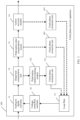
- FIG. 1 is a schematic structural diagram of an existing clock phase recovery apparatus.
- a clock phase recovery apparatus 100 may include an analog-to-digital converter 11, a dispersion compensation unit 12, a polarization state compensation circuit 13, a clock phase extraction unit, a loop filter 15, a voltage-controlled oscillator 16, and a carrier recovery module 14.
- the analog-to-digital converter 11 is configured to perform analog-to-digital conversion on an input analog signal, and then output a digital signal.
- the digital signal enters the polarization state compensation circuit 13 after passing through the dispersion compensation unit 12.
- the dispersion compensation unit 12 performs dispersion compensation.
- the dispersion compensation unit 12 usually includes two important modules: a fast Fourier transformation (Fast Fourier Transformation, FFT) module and an inverse fast Fourier transformation (Inverse Fast Fourier Transformation, IFFT) module.
- the polarization state compensation circuit 13 performs polarization mode dispersion (Polarization Mode Dispersion, PMD) compensation.
- the digital signal After signal impairment compensation is performed on the digital signal, the digital signal enters the carrier recovery module 14, so that carrier recovery (Carrier Recovery) is performed on the digital signal.
- the clock phase extraction unit completes calculation of an element phase error, and a calculated error signal may be fed back to the voltage-controlled oscillator 16 through the loop filter 15.
- the voltage-controlled oscillator 16 adjusts a clock phase to obtain a data element with an optimal sampling phase.
- the clock phase extraction unit may be disposed at different positions.
- a clock phase extraction unit 171 may be disposed at an output end of the dispersion compensation unit 12. Before a signal enters the clock phase extraction unit 171, a polarization state rotation of the signal is tracked and compensated by using a polarization rotation (Rotation) tracking module.
- the analog-to-digital converter 11, the dispersion compensation unit 12, the polarization rotation tracking module 172, the clock phase extraction unit 171, the loop filter 15, and the voltage-controlled oscillator 16 form a feedback loop, to complete adjustment of a sampling clock of the analog-to-digital converter 11.
- the dispersion compensation unit 12 needs to perform FFT and IFFT, resulting in a relatively long period of data processing time. Therefore, a clock recovery delay is very high, and system performance is affected.
- the polarization rotation tracking module 172 is difficult to be implemented in a scenario with great channel impairment. This reduces an impairment compensation effect of the polarization state rotation.
- a clock phase extraction unit 181 may be disposed at an output end of the polarization state compensation circuit 13.
- the analog-to-digital converter 11, the dispersion compensation unit 12, the polarization state compensation circuit 13, the clock phase extraction unit 181, the loop filter 15, and the voltage-controlled oscillator 16 form a feedback loop, to complete adjustment of the sampling clock of the analog-to-digital converter 11.
- the clock recovery delay is very high.
- a quantity of clock phases compensated by the polarization state compensation circuit 13 is the same as a quantity of phases that can be detected by the clock phase extraction unit 181. This usually results in a large signal phase offset and a large detection deviation, and reduces sensitivity of clock phase extraction.
- a clock phase extraction unit 191 may be disposed at an output end of the carrier recovery module 14.
- the analog-to-digital converter 11, the dispersion compensation unit 12, the polarization state compensation circuit 13, the carrier recovery module 14, the clock phase extraction unit 191, the loop filter 15, and the voltage-controlled oscillator 16 form a feedback loop, to complete adjustment of the sampling clock of the analog-to-digital converter 11. There are more modules in the feedback loop, and the clock recovery delay is higher.
- embodiments of this application provide a clock phase recovery apparatus and method, and a chip.
- a quantity of modules in the feedback loop is reduced to reduce a loop delay. This reduces a clock phase delay and improves the system performance.
- FIG. 2 is a schematic structural diagram of a clock phase recovery apparatus according to Embodiment 1 of this application.
- a clock phase recovery apparatus 200 provided in this embodiment may include: an analog-to-digital converter (ADC) 21, a dispersion compensation unit 22 (which may be denoted as CD EQ), a digital interpolator 23 (which may be denoted as Int.), a multiple-input multiple-output (Multiple-Input Multiple-Output, MIMO) equalization unit 24 (which may be denoted as MIMO EQ), and a clock offset phase obtaining unit 25.
- ADC analog-to-digital converter
- CD EQ dispersion compensation unit 22
- CD EQ digital interpolator 23
- MIMO Multiple-Input Multiple-Output
- MIMO Multiple-Input Multiple-Output equalization unit 24
- An output end of the analog-to-digital converter 21 is connected to an input end of the dispersion compensation unit 22, and an output end of the dispersion compensation unit 22 is connected to a first input end of the digital interpolator 23.
- An output end of the digital interpolator 23 is connected to an input end of the MIMO equalization unit 24, and an output end of the MIMO equalization unit 24 is connected to an input end of the clock offset phase obtaining unit 25.
- An output end of the clock offset phase obtaining unit 25 is connected to a second input end of the digital interpolator 23.
- the analog-to-digital converter 21 is configured to perform analog-to-digital conversion on an input analog signal, and output a second sampling signal.
- the dispersion compensation unit 22 is configured to perform dispersion compensation on the second sampling signal output by the analog-to-digital converter 21, and output a dispersion-compensated signal to the digital interpolator 23.
- the digital interpolator 23 is configured to adjust, based on first offset phase information output by the clock offset phase obtaining unit 25, the dispersion-compensated signal output by the dispersion compensation unit 22, so that a signal output by the digital interpolator 23 is a signal at an optimal sampling moment.
- the first offset phase information is determined by the clock offset phase obtaining unit 25 based on a tap coefficient of the MIMO equalization unit 24 and a first output signal output by the MIMO equalization unit 24.
- the first output signal is an output signal corresponding to a first sampling signal, and the first sampling signal is a previous adjacent sampling signal of the second sampling signal.
- the MIMO equalization unit 24 is configured to perform polarization mode dispersion compensation and equalization on the signal output by the digital interpolator 23, and output a second output signal.
- a principle of clock phase recovery is as follows.
- the analog-to-digital converter 21 samples the input analog signal, and outputs a sampling signal.
- two adjacent sampling signals may be respectively referred to as a first sampling signal and a second sampling signal.
- the first sampling signal is a previous adjacent sampling signal of the second sampling signal.
- the MIMO equalization unit 24 After the first sampling signal is processed by the dispersion compensation unit 22, the digital interpolator 23, and the MIMO equalization unit 24, the MIMO equalization unit 24 outputs the first output signal corresponding to the first sampling signal.
- the clock offset phase obtaining unit 25 determines the first offset phase information based on the first output signal and the tap coefficient of the MIMO equalization unit 24, and feeds back the first offset phase information to the second input end of the digital interpolator 23.
- the first offset phase information is used by the digital interpolator 23 to adjust a dispersion-compensated signal corresponding to the second sampling signal.
- the dispersion compensation unit 22 performs the dispersion compensation on the second sampling signal, and outputs the dispersion-compensated signal to the digital interpolator 23.
- the digital interpolator 23 has two input ends, which may be respectively referred to as the first input end and the second input end.
- the dispersion-compensated signal is input at the first input end of the digital interpolator 23, and the first offset phase information fed back by the clock offset phase obtaining unit 25 is input at the second input end of the digital interpolator 23.
- the digital interpolator 23 adjusts, based on the first offset phase information, the dispersion-compensated signal corresponding to the second sampling signal, so that the signal output by the digital interpolator 23 is the signal at the optimal sampling moment.
- a basic principle of the digital interpolator is as follows: When sampling frequency or a phase of the sampling signal is not ideal, for example, when the sampling frequency becomes higher or lower than reference frequency, or when a sampling location is not at an optimal point of an element waveform, the sampling signal may be adjusted by using an interpolation method to obtain an optimal sampling signal.
- the digital interpolator 23 adjusts, based on offset phase information fed back by the clock offset phase obtaining unit 25, a signal output by the dispersion compensation unit 22.
- the signal output by the digital interpolator 23 is input at the input end of the MIMO equalization unit 24.
- the MIMO equalization unit 24 performs the polarization mode dispersion compensation and equalization on the signal output by the digital interpolator 23, and outputs the second output signal corresponding to the second sampling signal.
- the second output signal is input at the input end of the clock offset phase obtaining unit 25.
- the clock offset phase obtaining unit 25 determines second offset phase information based on the second output signal and the tap coefficient of the MIMO equalization unit 24, and feeds back the second offset phase information to the second input end of the digital interpolator 23.
- the second offset phase information is used by the digital interpolator 23 to adjust a dispersion-compensated signal corresponding to a third sampling signal.
- the third sampling signal is output by the analog-to-digital converter 21 and is a next adjacent sampling signal of the second sampling signal.
- the digital interpolator is disposed between the dispersion compensation unit and the MIMO equalization unit.
- the digital interpolator, the MIMO equalization unit, and the clock offset phase obtaining unit form a feedback loop to complete a clock phase adjustment.
- the dispersion compensation unit is not included. Therefore, a delay caused by FFT and IFFT calculation is avoided, and a loop delay is reduced. This reduces a clock phase delay and improves system performance.
- the clock phase delay is further reduced.
- polarization mode dispersion compensation and equalization are performed on a signal by using the MIMO equalization unit. This reduces damage impact on the signal caused by polarization state rotation and improves a compensation effect.
- the clock offset phase obtaining unit determines offset phase information based on an output signal from the MIMO equalization unit and the tap coefficient of the MIMO equalization unit. This improves sensitivity and accuracy of clock phase extraction.
- there is a small quantity of modules in the feedback loop This reduces the clock phase delay and improves the system performance.
- the analog-to-digital converter 21 is configured to perform the analog-to-digital conversion on the analog signal
- the dispersion compensation unit 22 is configured to perform the dispersion compensation
- the MIMO equalization unit 24 is configured to perform the polarization mode dispersion compensation and equalization.
- the digital interpolator 23 may be implemented by using any existing circuit, chip, unit, module, or device that implements a corresponding function. This is not limited in this embodiment.
- the clock phase recovery apparatus 200 provided in this embodiment may further include a carrier recovery unit 26 (which may be denoted as CR).
- a carrier recovery unit 26 (which may be denoted as CR).
- An input end of the carrier recovery unit 26 is connected to the output end of the MIMO equalization unit 24.
- the carrier recovery unit 26 is configured to perform carrier recovery on the output signal output by the MIMO equalization unit 24, and output a carrier-recovered signal.
- the MIMO equalization unit 24 outputs the first output signal corresponding to the first sampling signal.
- the carrier recovery unit 26 is configured to perform carrier recovery on the first output signal output by the MIMO equalization unit 24, and output a carrier-recovered signal.
- the MIMO equalization unit 24 outputs the second output signal corresponding to the second sampling signal.
- the carrier recovery unit 26 is configured to perform carrier recovery on the second output signal output by the MIMO equalization unit 24, and output a carrier-recovered signal.
- the carrier recovery unit 26 is configured to perform the carrier recovery, and may be implemented by using any existing circuit, chip, unit, module, or device that implements a corresponding function. This is not limited in this embodiment.
- This embodiment provides the clock phase recovery apparatus, and the clock phase recovery apparatus includes the analog-to-digital converter, the dispersion compensation unit, the digital interpolator, the MIMO equalization unit, and the clock offset phase obtaining unit.
- the digital interpolator, the MIMO equalization unit, and the clock offset phase obtaining unit form the feedback loop to complete the clock phase adjustment. There is a small quantity of modules in the feedback loop. Therefore, this reduces the clock phase delay and improves the system performance.
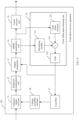
- FIG. 3 is a schematic structural diagram of a clock phase recovery apparatus according to Embodiment 2 of this application. Based on the embodiment shown in FIG. 2 , this embodiment provides another implementation of the clock phase recovery apparatus. As shown in FIG. 3 , the clock phase recovery apparatus 200 provided in this embodiment may include the analog-to-digital converter 21, the dispersion compensation unit 22, the digital interpolator 23, the MIMO equalization unit 24, and the clock offset phase obtaining unit 25.
- the clock phase recovery apparatus 200 may further include a voltage-controlled oscillator (VCO) 28 and a loop filter 27 (which may be denoted as a loop filter).
- VCO voltage-controlled oscillator
- loop filter 27 which may be denoted as a loop filter
- the output end of the clock offset phase obtaining unit 25 is further connected to an input end of the loop filter 27, an output end of the loop filter 27 is connected to an input end of the voltage-controlled oscillator 28, and an output end of the voltage-controlled oscillator 28 is connected to the analog-to-digital converter 21.
- the loop filter 27 is configured to perform loop low-pass filtering on the first offset phase information output by the clock offset phase obtaining unit 25 to convert the first offset phase information into a voltage control signal.
- the voltage-controlled oscillator 28 is configured to determine a clock adjustment signal based on the voltage control signal output by the loop filter 27.
- the digital interpolator 23, the MIMO equalization unit 24, and the clock offset phase obtaining unit 25 form a inner feedback loop (or referred to as a digital interpolator path), to complete adjustment of a clock phase.
- the clock offset phase obtaining unit 25, the voltage-controlled oscillator 28, and the loop filter 27 form a outer feedback loop (or referred to as a voltage-controlled oscillator adjustment path), and sampling frequency of the analog-to-digital converter 21 may be adjusted by adjusting the voltage-controlled oscillator 28.
- a signal that is input into the inner feedback loop is a signal with adjusted sampling frequency. Therefore, accuracy and an effect of clock phase recovery are further improved.
- the voltage-controlled oscillator adjustment path is a path with a relatively low adjustment speed. A delay of an entire loop still depends on the digital interpolator 23. Therefore, compared with the prior art, the clock phase recovery apparatus provided in this embodiment can reduce a clock phase delay is reduced, and improve system performance.
- loop filter 27 and the voltage-controlled oscillator 28 in this embodiment may be implemented by using any existing circuit, chip, unit, module, or device that implements a corresponding function. This is not limited in this embodiment.
- analog-to-digital converter 21 is specifically configured to:
- This embodiment provides the clock phase recovery apparatus, and the clock phase recovery apparatus includes the analog-to-digital converter, the dispersion compensation unit, the digital interpolator, the MIMO equalization unit, the clock offset phase obtaining unit, the voltage-controlled oscillator, and the loop filter.
- the digital interpolator, the MIMO equalization unit, and the clock offset phase obtaining unit form the feedback loop to complete the clock phase adjustment. There is a small quantity of modules in the feedback loop. Therefore, this reduces the clock phase delay and improves the system performance.
- the sampling frequency of the analog-to-digital converter is adjusted by using the voltage-controlled oscillator and the loop filter. This further improves accuracy of clock phase recovery.
- FIG. 4 is a schematic structural diagram of a clock phase recovery apparatus according to Embodiment 3 of this application. Based on the embodiments shown in FIG. 2 and FIG. 3 , this embodiment provides a specific implementation of the clock phase recovery apparatus, and in particular, provides a specific implementation of a clock offset phase obtaining unit. As shown in FIG. 4 , the clock phase recovery apparatus 200 provided in this embodiment may include the analog-to-digital converter 21, the dispersion compensation unit 22, the digital interpolator 23, the MIMO equalization unit 24, and the clock offset phase obtaining unit 25.
- the clock offset phase obtaining unit 25 may include a decoupling module 251 (which may be denoted as Uncoupling), a clock phase detector 252 (which may be denoted as Phase Det.), an adder 253, and a filter 254 (which may be denoted as a Loop Filter).
- a decoupling module 251 which may be denoted as Uncoupling
- a clock phase detector 252 which may be denoted as Phase Det.
- an adder 253 which may be denoted as a Loop Filter
- a first output end of the MIMO equalization unit 24 is connected to an input end of the decoupling module 251, and a second output end of the MIMO equalization unit 24 is connected to an input end of the clock phase detector 252.
- the output end of the MIMO equalization unit 24 and an output end of the clock phase detector 252 are separately connected to an input end of the adder 253.
- An output end of the adder 253 is connected to an input end of the filter 254, and an output end of the filter 254 is connected to the second input end of the digital interpolator 23.
- the decoupling module 251 is configured to determine a compensated clock phase based on the tap coefficient of the MIMO equalization unit 24, and output the compensated clock phase to the adder 253.
- the clock phase detector 252 is configured to obtain a clock phase of the first output signal output by the MIMO equalization unit 24, and output the clock phase of the first output signal to the adder 253.
- the adder 253 is configured to obtain a clock offset phase based on the compensated clock phase output by the decoupling module 251 and the clock phase that is of the first output signal and that is output by the clock phase detector 252, and output the clock offset phase to the filter 254.
- the filter 254 is configured to perform high frequency filtering on the clock offset phase output by the adder 253 to obtain the first offset phase information, and output the first offset phase information to the digital interpolator 23.
- a principle of clock phase recovery is as follows.
- the analog-to-digital converter 21 samples the input analog signal. According to an output sequence of a sampling signal, two adjacent sampling signals may be respectively referred to as a first sampling signal and a second sampling signal.
- the MIMO equalization unit 24 After the first sampling signal is processed by the dispersion compensation unit 22, the digital interpolator 23, and the MIMO equalization unit 24, the MIMO equalization unit 24 outputs the first output signal corresponding to the first sampling signal.
- the decoupling module 251 determines the compensated clock phase based on the tap coefficient of the MIMO equalization unit 24.
- the clock phase detector 252 obtains the clock phase of the first output signal.
- the adder 253 obtains an accurate first clock offset phase based on the input compensated clock phase and the clock phase of the first output signal.
- the filter 254 performs high frequency filtering on the accurate clock offset phase to further improve accuracy of filtered first offset phase information.
- the filter 254 feeds back the first offset phase information to the second input end of the digital interpolator 23.
- the first offset phase information is used by the digital interpolator 23 to adjust the dispersion-compensated signal corresponding to the second sampling signal.
- the dispersion compensation unit 22 After the second sampling signal is processed by the dispersion compensation unit 22, the dispersion compensation unit 22 outputs the dispersion-compensated signal to the digital interpolator 23.
- the digital interpolator 23 adjusts, based on the first offset phase information, the dispersion-compensated signal corresponding to the second sampling signal, so that the signal output by the digital interpolator 23 is the signal at the optimal sampling moment.
- the MIMO equalization unit 24 performs polarization mode dispersion compensation and equalization on the signal output by the digital interpolator 23, and outputs the second output signal corresponding to the second sampling signal.
- the decoupling module 251, the clock phase detector 252, the adder 253, and the filter 254 perform the foregoing processing on the second output signal to obtain the second offset phase information, and the second offset phase information is fed back to the second input end of the digital interpolator 23.
- the second offset phase information is used by the digital interpolator 23 to adjust the dispersion-compensated signal corresponding to the third sampling signal.
- the third sampling signal is output by the analog-to-digital converter 21 and is the next adjacent sampling signal of the second sampling signal.
- the MIMO equalization unit 24 performs specific compensation on clock offset of a signal. For example, an original phase change speed of the signal is A, and a phase change speed a is compensated by the MIMO equalization unit 24 for the phase change speed A. In this way, an output phase change speed of the signal is A - a.
- the decoupling module 251 determines a compensated clock phase a of the MIMO equalization unit 24 based on the tap coefficient of the MIMO equalization unit 24.
- the clock phase detector 252 obtains the clock phase A - a of the first output signal output by the MIMO equalization unit 24.
- the digital interpolator, the MIMO equalization unit, the decoupling module, the clock phase detector, the adder, and the filter form a feedback loop (or referred to as a digital interpolator path), to complete a clock phase adjustment.
- a feedback loop or referred to as a digital interpolator path
- an adjustment speed of the digital interpolator is relatively fast, and there is only one filter in the digital interpolator path. Therefore, this further reduces the clock phase delay.
- the decoupling module 251 is configured to determine a quantity of clock phases compensated by the MIMO equalization unit 24, and the clock phase detector 252 is configured to extract a clock phase of a signal.
- the adder 253 and the filter 254 may be implemented by using any existing circuit, chip, unit, module, or device that implements a corresponding function. This is not limited in this embodiment.
- the clock phase detector 252 may be a phase detector.
- Wxx, Wyy, Wyx, and Wxy are tap coefficients of the MIMO equalization unit 24, and angle () represents a phase function.
- the MIMO equalization unit 24 may have two input ends and two output ends. A signal in a polarization state may be separately input at the two input ends. Correspondingly, a signal in a polarization state may be separately output at the two output ends.
- the MIMO equalization unit 24 has the four tap coefficients: Wxx, Wyy, Wyx, and Wxy; and x and y may represent different polarization states, or are used to distinguish different inputs and outputs.
- this embodiment provides an implementation in which a clock phase compensated by the MIMO equalization unit 24 is determined based on the tap coefficient of the MIMO equalization unit 24 when the MIMO equalization unit 24 has the two input ends and the two output ends.
- a quantity of tap coefficients of the MIMO equalization unit 24 may be another implementation. This is not limited in this embodiment.
- the clock phase recovery apparatus 200 provided in this embodiment may further include the carrier recovery unit 26.
- the input end of the carrier recovery unit 26 is connected to the output end of the MIMO equalization unit 24.
- the carrier recovery unit 26 is configured to perform carrier recovery on an output signal output by the MIMO equalization unit 24, and output a carrier-recovered signal.
- the clock phase recovery apparatus 200 provided in this embodiment may further include the voltage-controlled oscillator 28 and the loop filter 27.
- the output end of the clock offset phase obtaining unit 25 is further connected to the input end of the loop filter 27, the output end of the loop filter 27 is connected to the input end of the voltage-controlled oscillator 28, and the output end of the voltage-controlled oscillator 28 is connected to the analog-to-digital converter 21.
- the loop filter 27 is configured to perform the loop low-pass filtering on the first offset phase information output by the clock offset phase obtaining unit 25 to convert the first offset phase information into the voltage control signal.
- the voltage-controlled oscillator 28 is configured to determine the clock adjustment signal based on the voltage control signal output by the loop filter 27.
- analog-to-digital converter 21 is specifically configured to:
- This embodiment provides the clock phase recovery apparatus, and the clock phase recovery apparatus includes the analog-to-digital converter, the dispersion compensation unit, the digital interpolator, the MIMO equalization unit, and the clock offset phase obtaining unit.
- the clock offset phase obtaining unit includes the decoupling module, the clock phase detector, the adder, and the filter.
- the digital interpolator, the MIMO equalizing unit, the decoupling module, the clock phase detector, the adder and the filter form the feedback loop to implement the clock phase adjustment. There is a small quantity of modules in the feedback loop. Therefore, this reduces the clock phase delay and improves the system performance.
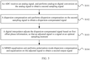
- FIG. 5 is a schematic flowchart of a clock phase recovery method according to Embodiment 1 of this application. As shown in FIG. 5 , the clock phase recovery method provided in this embodiment may be applied to a clock phase recovery apparatus.
- the clock phase recovery apparatus includes an ADC, a dispersion compensation unit, a digital interpolator, a MIMO equalization unit, and a clock offset phase obtaining unit.
- An output end of the ADC is connected to an input end of the dispersion compensation unit, and an output end of the dispersion compensation unit is connected to a first input end of the digital interpolator.
- An output end of the digital interpolator is connected to an input end of the MIMO equalization unit, and an output end of the MIMO equalization unit is connected to an input end of the clock offset phase obtaining unit.
- An output end of the clock offset phase obtaining unit is connected to a second input end of the digital interpolator.
- the clock phase recovery method provided in this embodiment may include the following steps.
- the ADC receives an analog signal, and performs analog-to-digital conversion on the analog signal to obtain a second sampling signal.
- the dispersion compensation unit performs dispersion compensation on the second sampling signal to obtain a dispersion-compensated signal.
- the digital interpolator adjusts the dispersion-compensated signal based on first offset phase information, so that an adjusted signal is a signal at an optimal sampling moment.
- the first offset phase information is determined by the clock offset phase obtaining unit based on a tap coefficient of the MIMO equalization unit and a first output signal.
- the first output signal is an output signal corresponding to a first sampling signal, and the first sampling signal is a previous adjacent sampling signal of the second sampling signal.
- the MIMO equalization unit performs polarization mode dispersion compensation and equalization on the adjusted signal to obtain a second output signal.
- the clock offset phase obtaining unit includes a decoupling module, a clock phase detector, an adder, and a filter.
- a first output end of the MIMO equalization unit is connected to an input end of the decoupling module, and a second output end of the MIMO equalization unit is connected to an input end of the clock phase detector.
- the output end of the MIMO equalization unit and an output end of the clock phase detector are separately connected to an input end of the adder.
- An output end of the adder is connected to an input end of the filter, and an output end of the filter is connected to the second input end of the digital interpolator.
- That the clock offset phase obtaining unit determines the first offset phase information based on the tap coefficient of the MIMO equalization unit and the first output signal may include:
- the clock phase recovery apparatus may further include a carrier recovery unit, and an input end of the carrier recovery unit is connected to the output end of the MIMO equalization unit.
- the clock phase recovery method provided in this embodiment may further include: performing, by the carrier recovery unit, carrier recovery on the second output signal to obtain a carrier-recovered signal.
- the clock phase recovery apparatus may further include a VCO and a loop filter.
- the output end of the clock offset phase obtaining unit is further connected to an input end of the loop filter, an output end of the loop filter is connected to an input end of the VCO, and an output end of the VCO is connected to the ADC.
- the ADC performs the analog-to-digital conversion on the analog signal to obtain the second sampling signal may include:
- the clock phase recovery method provided in this embodiment of this application may be applied to the clock phase recovery apparatus provided in the embodiments shown in FIG. 2 to FIG. 4 .
- Technical principles and technical effects thereof are similar, and details are not described herein again.
- An embodiment of this application further provides a chip, including the clock phase recovery apparatus provided in the apparatus embodiments of this application.
- the chip provided in this embodiment of this application includes the clock phase recovery apparatus provided in the embodiments shown in FIG. 2 to FIG. 4 .
- Technical principles and technical effects thereof are similar, and details are not described herein again.
Landscapes
- Engineering & Computer Science (AREA)
- Computer Networks & Wireless Communication (AREA)
- Signal Processing (AREA)
- Physics & Mathematics (AREA)
- Electromagnetism (AREA)
- Stabilization Of Oscillater, Synchronisation, Frequency Synthesizers (AREA)
- Synchronisation In Digital Transmission Systems (AREA)
Description
- Embodiments of this application relate to the communications technologies field, and in particular, to a clock phase recovery apparatus and method, and a chip.
- In an optical communications system, after optical-to-electrical conversion is performed at a receive end, algorithmic processing in a digital domain needs to be performed. A rate at which the algorithm processing is performed at the receive end needs to keep synchronous with a rate at which a transmit end sends data, to ensure that all transmitted data is processed in time. In other words, the transmit end and receive end need to ensure clock synchronization. If a synchronization deviation occurs between a clock of the transmit end and a clock of the receive end, the clocks need to be recovered to ensure that sampled data at the receive end is exactly at an optimal decision point of a signal element, to implement data synchronization between the receive end and the transmit end. It can be learned that clock recovery is an integral part of a communications system, and performance of the clock recovery directly affects system performance.
- Currently, a clock phase recovery apparatus may be implemented in an analog circuit, or may be implemented in a digital circuit. When the clock phase recovery apparatus is implemented by using the digital circuit, the clock phase recovery apparatus usually includes an analog-to-digital converter (Analog-to-Digital Converter, ADC for short), a dispersion compensation unit, a polarization state compensation circuit, a clock phase extraction unit, a loop filter, and a voltage-controlled oscillator
- (Voltage-Controlled Oscillator, VCO for short). The clock phase extraction unit completes calculation of an element phase error, and a calculated error signal may be fed back to the VCO through the loop filter. The VCO adjusts a clock phase to obtain a data element with an optimal sampling phase.
- However, in an entire loop, there are many modules for A/D conversion, clock phase extraction, loop filtering, and VCO control, resulting in a high clock recovery delay. This affects the system performance.
THIGO F PORTELA ET AL: "Novel Non-Data-Aided Clock Recovery Method for DP-QPSK Systems With CMA Equalizers", IEEE PHOTONICS TECHNOLOGY LETTERS, vol. 24, no.19, 1 October 2012, pages 1696-1699, XP011460853 discloses discloses a TED (time error detector, also referred to as TED-EQ) using information from four equalizer filters, the synchronization performance and algorithm convergence speed are determined by the number of equalizer taps,Fig.2 discloses an equalizer including four Ntaps long FIR filters (i.e. WHV , WVH , WHH , WVV ) arranged in a typical butterfly architecture, the equalizer is connected to the TED, in equations (3), (4) and (5), coefficients of filters WXX (XX=HV, VH, HH or VV) are used to compute the timing error in the TED.
US 8 737 847 B2 discloses an apparatus and method for performing joint equalization and timing recovery in coherent optical systems. The method includes equalizing signals to generate compensated polarization signals, wherein timing error in a distorted optical signal is calculated based on one of the compensated polarization signals. The method further includes performing resampling polarization signals to correct timing offset in an optical signal based on the calculated timing error. - Embodiments of this application provide a clock phase recovery apparatus and method, and a chip, to reduce a clock phase delay and improve system performance.
- According to a first aspect, an embodiment of this application provides a clock phase recovery apparatus, including an ADC, a dispersion compensation unit, a digital interpolator, a MIMO equalization unit, and a clock offset phase obtaining unit. An output end of the ADC is connected to an input end of the dispersion compensation unit, and an output end of the dispersion compensation unit is connected to a first input end of the digital interpolator. An output end of the digital interpolator is connected to an input end of the MIMO equalization unit, and an output end of the MIMO equalization unit is connected to an input end of the clock offset phase obtaining unit. An output end of the clock offset phase obtaining unit is connected to a second input end of the digital interpolator. The ADC is configured to perform analog-to-digital conversion on an input analog signal, and output a second sampling signal. The dispersion compensation unit is configured to perform dispersion compensation on the second sampling signal output by the ADC, and output a dispersion-compensated signal to the digital interpolator. The digital interpolator is configured to adjust, based on first offset phase information output by the clock offset phase obtaining unit, the dispersion-compensated signal output by the dispersion compensation unit, so that a signal output by the digital interpolator is a signal at an optimal sampling moment. The first offset phase information is determined by the clock offset phase obtaining unit based on a tap coefficient of the MIMO equalization unit and a first output signal output by the MIMO equalization unit. The first output signal is an output signal corresponding to a first sampling signal, and the first sampling signal is a previous adjacent sampling signal of the second sampling signal. The MIMO equalization unit is configured to perform polarization mode dispersion compensation and equalization on the signal output by the digital interpolator, and output a second output signal, wherein the clock offset phase obtaining unit includes a decoupling module, a clock phase detector, an adder, and a filter. A first output end of the MIMO equalization unit is connected to an input end of the decoupling module, and a second output end of the MIMO equalization unit is connected to an input end of the clock phase detector. The output end of the MIMO equalization unit and an output end of the clock phase detector are separately connected to an input end of the adder. An output end of the adder is connected to an input end of the filter, and an output end of the filter is connected to the second input end of the digital interpolator. The decoupling module is configured to determine a compensated clock phase based on the tap coefficient of the MIMO equalization unit, and output the compensated clock phase to the adder. The clock phase detector is configured to obtain a clock phase of the first output signal output by the MIMO equalization unit, and output the clock phase of the first output signal to the adder. The adder is configured to obtain a clock offset phase based on the compensated clock phase output by the decoupling module and the clock phase that is of the first output signal and that is output by the clock phase detector, and output the clock offset phase to the filter. The filter is configured to perform high frequency filtering on the clock offset phase output by the adder to obtain the first offset phase information, and output the first offset phase information to the digital interpolator.
- The apparatus is defined by claim 1.
- According to the clock phase recovery apparatus provided in the first aspect, the digital interpolator is disposed between the dispersion compensation unit and the MIMO equalization unit. The digital interpolator, the MIMO equalization unit, and the clock offset phase obtaining unit form a feedback loop to complete a clock phase adjustment. There is a small quantity of modules in the feedback loop, and in particular, the dispersion compensation unit is not included. Therefore, a delay caused by FFT and IFFT calculation is avoided, and a loop delay is reduced. This reduces a clock phase delay and improves system performance. In addition, because an adjustment speed of the digital interpolator is relatively fast, the clock phase delay is further reduced.
- Optionally, in a possible implementation of the first aspect, the decoupling module is specifically configured to determine the compensated clock phase a according to a = angle (Wxx * Wyy - Wyx * Wxy). Wxx, Wyy, Wyx, and Wxy are tap coefficients of the MIMO equalization unit, and angle () represents a phase function.
- Optionally, in a possible implementation of the first aspect, the clock phase detector is a phase detector.
- Optionally, in a possible implementation of the first aspect, the apparatus further includes a carrier recovery unit. An input end of the carrier recovery unit is connected to the output end of the MIMO equalization unit. The carrier recovery unit is configured to perform carrier recovery on the second output signal output by the MIMO equalization unit, and output a carrier-recovered signal.
- Optionally, in a possible implementation of the first aspect, the apparatus further includes a voltage-controlled oscillator VCO and a loop filter. The output end of the clock offset phase obtaining unit is further connected to an input end of the loop filter, an output end of the loop filter is connected to an input end of the VCO, and an output end of the VCO is connected to the ADC. The loop filter is configured to perform loop low-pass filtering on the first offset phase information output by the clock offset phase obtaining unit to convert the first offset phase information into a voltage control signal. The VCO is configured to determine a clock adjustment signal based on the voltage control signal output by the loop filter.
- Optionally, in a possible implementation of the first aspect, the ADC is specifically configured to adjust sampling frequency based on the clock adjustment signal output by the VCO, and perform the analog-to-digital conversion on the analog signal based on adjusted sampling frequency to obtain the second sampling signal.
- According to a second aspect, an embodiment of this application provides a clock phase recovery method, applied to a clock phase recovery apparatus. The clock phase recovery apparatus includes an analog-to-digital converter ADC, a dispersion compensation unit, a digital interpolator, a multiple-input multiple-output MIMO equalization unit, and a clock offset phase obtaining unit. An output end of the ADC is connected to an input end of the dispersion compensation unit, and an output end of the dispersion compensation unit is connected to a first input end of the digital interpolator. An output end of the digital interpolator is connected to an input end of the MIMO equalization unit, and an output end of the MIMO equalization unit is connected to an input end of the clock offset phase obtaining unit. An output end of the clock offset phase obtaining unit is connected to a second input end of the digital interpolator. The method includes: receiving, by the ADC, an analog signal, and performing analog-to-digital conversion on the analog signal to obtain a second sampling signal; performing, by the dispersion compensation unit, dispersion compensation on the second sampling signal to obtain a dispersion-compensated signal; adjusting, by the digital interpolator, the dispersion-compensated signal based on first offset phase information, so that an adjusted signal is a signal at an optimal sampling moment, where the first offset phase information is determined by the clock offset phase obtaining unit based on a tap coefficient of the MIMO equalization unit and a first output signal, the first output signal is an output signal corresponding to a first sampling signal, and the first sampling signal is a previous adjacent sampling signal of the second sampling signal; and performing, by the MIMO equalization unit, polarization mode dispersion compensation and equalization on the adjusted signal to obtain a second output signal, wherein the clock offset phase obtaining unit includes a decoupling module, a clock phase detector, an adder, and a filter. A first output end of the MIMO equalization unit is connected to an input end of the decoupling module, and a second output end of the MIMO equalization unit is connected to an input end of the clock phase detector. The output end of the MIMO equalization unit and an output end of the clock phase detector are separately connected to an input end of the adder. An output end of the adder is connected to an input end of the filter, and an output end of the filter is connected to the second input end of the digital interpolator. That the clock offset phase obtaining unit determines the first offset phase information based on the tap coefficient of the MIMO equalization unit and the first output signal includes: determining, by the decoupling module, a compensated clock phase based on the tap coefficient of the MIMO equalization unit; obtaining, by the clock phase detector, a clock phase of the first output signal; obtaining, by the adder, a clock offset phase based on the compensated clock phase and the clock phase of the first output signal; and performing, by the filter, high frequency filtering on the clock offset phase to obtain the first offset phase information,
- The method is defined by independent claim 7
- Optionally, in a possible implementation of the second aspect, the determining, by the decoupling module, a compensated clock phase based on the tap coefficient of the MIMO equalization unit includes: determining, by the decoupling module, the compensated clock phase a according to a = angle (Wxx * Wyy - Wyx * Wxy), where Wxx, Wyy, Wyx, and Wxy are tap coefficients of the MIMO equalization unit, and angle () represents a phase function.
- Optionally, in a possible implementation of the second aspect, the clock phase recovery apparatus further includes a carrier recovery unit, and an input end of the carrier recovery unit is connected to the output end of the MIMO equalization unit. The method further includes: performing, by the carrier recovery unit, carrier recovery on the second output signal to obtain a carrier-recovered signal.
- Optionally, in a possible implementation of the second aspect, the clock phase recovery apparatus further includes a voltage-controlled oscillator VCO and a loop filter. The output end of the clock offset phase obtaining unit is further connected to an input end of the loop filter, an output end of the loop filter is connected to an input end of the VCO, and an output end of the VCO is connected to the ADC. The method further includes: performing, by the loop filter, loop low-pass filtering on the first offset phase information to convert the first offset phase information into a voltage control signal; and determining, by the VCO, a clock adjustment signal based on the voltage control signal.
- Optionally, in a possible implementation of the second aspect, the performing, by the ADC, analog-to-digital conversion on the analog signal to obtain a second sampling signal includes: adjusting, by the ADC, sampling frequency based on the clock adjustment signal; and performing, by the ADC, the analog-to-digital conversion on the analog signal based on adjusted sampling frequency to obtain the second sampling signal.
- According to a third aspect, an embodiment of this application provides a chip, including the clock phase recovery apparatus according to any implementation of the first aspect of this application.
- Embodiments of this application provide the clock phase recovery apparatus and method, and the chip. The clock phase recovery apparatus includes the ADC, the dispersion compensation unit, the digital interpolator, the MIMO equalization unit, and the clock offset phase obtaining unit. The digital interpolator, the MIMO equalization unit, and the clock offset phase obtaining unit form the feedback loop to complete the clock phase adjustment. There is a small quantity of modules in the feedback loop, and the loop delay is reduced. Therefore, this reduces the clock phase delay and improves the system performance.
-
-
FIG. 1 is a schematic structural diagram of an existing clock phase recovery apparatus; -
FIG. 2 is a schematic structural diagram of a clock phase recovery apparatus according to Embodiment 1 of this application; -
FIG. 3 is a schematic structural diagram of a clock phase recovery apparatus according to Embodiment 2 of this application; -
FIG. 4 is a schematic structural diagram of a clock phase recovery apparatus according to Embodiment 3 of this application; and -
FIG. 5 is a schematic flowchart of a clock phase recovery method according to Embodiment 1 of this application. - Embodiments 1 and 2 do not fall under the scope of the claims.
-
FIG. 1 is a schematic structural diagram of an existing clock phase recovery apparatus. As shown inFIG. 1 , a clockphase recovery apparatus 100 may include an analog-to-digital converter 11, adispersion compensation unit 12, a polarizationstate compensation circuit 13, a clock phase extraction unit, aloop filter 15, a voltage-controlledoscillator 16, and acarrier recovery module 14. - The analog-to-
digital converter 11 is configured to perform analog-to-digital conversion on an input analog signal, and then output a digital signal. The digital signal enters the polarizationstate compensation circuit 13 after passing through thedispersion compensation unit 12. Thedispersion compensation unit 12 performs dispersion compensation. Thedispersion compensation unit 12 usually includes two important modules: a fast Fourier transformation (Fast Fourier Transformation, FFT) module and an inverse fast Fourier transformation (Inverse Fast Fourier Transformation, IFFT) module. The polarizationstate compensation circuit 13 performs polarization mode dispersion (Polarization Mode Dispersion, PMD) compensation. After signal impairment compensation is performed on the digital signal, the digital signal enters thecarrier recovery module 14, so that carrier recovery (Carrier Recovery) is performed on the digital signal. The clock phase extraction unit completes calculation of an element phase error, and a calculated error signal may be fed back to the voltage-controlledoscillator 16 through theloop filter 15. The voltage-controlledoscillator 16 adjusts a clock phase to obtain a data element with an optimal sampling phase. - In
FIG. 1 , the clock phase extraction unit may be disposed at different positions. - In an implementation, a clock
phase extraction unit 171 may be disposed at an output end of thedispersion compensation unit 12. Before a signal enters the clockphase extraction unit 171, a polarization state rotation of the signal is tracked and compensated by using a polarization rotation (Rotation) tracking module. In this implementation, the analog-to-digital converter 11, thedispersion compensation unit 12, the polarizationrotation tracking module 172, the clockphase extraction unit 171, theloop filter 15, and the voltage-controlledoscillator 16 form a feedback loop, to complete adjustment of a sampling clock of the analog-to-digital converter 11. However, there are many modules in the feedback loop, and thedispersion compensation unit 12 needs to perform FFT and IFFT, resulting in a relatively long period of data processing time. Therefore, a clock recovery delay is very high, and system performance is affected. In addition, the polarizationrotation tracking module 172 is difficult to be implemented in a scenario with great channel impairment. This reduces an impairment compensation effect of the polarization state rotation. - In another implementation, a clock
phase extraction unit 181 may be disposed at an output end of the polarizationstate compensation circuit 13. In this implementation, the analog-to-digital converter 11, thedispersion compensation unit 12, the polarizationstate compensation circuit 13, the clockphase extraction unit 181, theloop filter 15, and the voltage-controlledoscillator 16 form a feedback loop, to complete adjustment of the sampling clock of the analog-to-digital converter 11. There are many modules in the feedback loop, and the clock recovery delay is very high. In addition, a quantity of clock phases compensated by the polarizationstate compensation circuit 13 is the same as a quantity of phases that can be detected by the clockphase extraction unit 181. This usually results in a large signal phase offset and a large detection deviation, and reduces sensitivity of clock phase extraction. - In still another implementation, a clock
phase extraction unit 191 may be disposed at an output end of thecarrier recovery module 14. In this implementation, the analog-to-digital converter 11, thedispersion compensation unit 12, the polarizationstate compensation circuit 13, thecarrier recovery module 14, the clockphase extraction unit 191, theloop filter 15, and the voltage-controlledoscillator 16 form a feedback loop, to complete adjustment of the sampling clock of the analog-to-digital converter 11. There are more modules in the feedback loop, and the clock recovery delay is higher. - It can be learned that in a clock phase recovery process, there are many modules in an entire loop of the existing clock phase recovery apparatus. This results in a very high clock recovery delay and affects the system performance.
- To resolve the foregoing technical problem, embodiments of this application provide a clock phase recovery apparatus and method, and a chip. In the clock phase recovery process, a quantity of modules in the feedback loop is reduced to reduce a loop delay. This reduces a clock phase delay and improves the system performance.
- The following describes in detail, by using specific embodiments, technical solutions of this application and how to resolve the foregoing technical problem by using the technical solutions of this application. The following specific embodiments may be combined with one another. Same or similar concepts or processes may not be described in detail in some embodiments.
-
FIG. 2 is a schematic structural diagram of a clock phase recovery apparatus according to Embodiment 1 of this application. As shown inFIG. 2 , a clockphase recovery apparatus 200 provided in this embodiment may include:
an analog-to-digital converter (ADC) 21, a dispersion compensation unit 22 (which may be denoted as CD EQ), a digital interpolator 23 (which may be denoted as Int.), a multiple-input multiple-output (Multiple-Input Multiple-Output, MIMO) equalization unit 24 (which may be denoted as MIMO EQ), and a clock offsetphase obtaining unit 25. - An output end of the analog-to-
digital converter 21 is connected to an input end of thedispersion compensation unit 22, and an output end of thedispersion compensation unit 22 is connected to a first input end of thedigital interpolator 23. An output end of thedigital interpolator 23 is connected to an input end of theMIMO equalization unit 24, and an output end of theMIMO equalization unit 24 is connected to an input end of the clock offsetphase obtaining unit 25. An output end of the clock offsetphase obtaining unit 25 is connected to a second input end of thedigital interpolator 23. - The analog-to-
digital converter 21 is configured to perform analog-to-digital conversion on an input analog signal, and output a second sampling signal. - The
dispersion compensation unit 22 is configured to perform dispersion compensation on the second sampling signal output by the analog-to-digital converter 21, and output a dispersion-compensated signal to thedigital interpolator 23. - The
digital interpolator 23 is configured to adjust, based on first offset phase information output by the clock offsetphase obtaining unit 25, the dispersion-compensated signal output by thedispersion compensation unit 22, so that a signal output by thedigital interpolator 23 is a signal at an optimal sampling moment. The first offset phase information is determined by the clock offsetphase obtaining unit 25 based on a tap coefficient of theMIMO equalization unit 24 and a first output signal output by theMIMO equalization unit 24. The first output signal is an output signal corresponding to a first sampling signal, and the first sampling signal is a previous adjacent sampling signal of the second sampling signal. - The
MIMO equalization unit 24 is configured to perform polarization mode dispersion compensation and equalization on the signal output by thedigital interpolator 23, and output a second output signal. - In this embodiment, a principle of clock phase recovery is as follows.
- The analog-to-
digital converter 21 samples the input analog signal, and outputs a sampling signal. According to an output sequence of the sampling signal, two adjacent sampling signals may be respectively referred to as a first sampling signal and a second sampling signal. In other words, the first sampling signal is a previous adjacent sampling signal of the second sampling signal. - After the first sampling signal is processed by the
dispersion compensation unit 22, thedigital interpolator 23, and theMIMO equalization unit 24, theMIMO equalization unit 24 outputs the first output signal corresponding to the first sampling signal. The clock offsetphase obtaining unit 25 determines the first offset phase information based on the first output signal and the tap coefficient of theMIMO equalization unit 24, and feeds back the first offset phase information to the second input end of thedigital interpolator 23. The first offset phase information is used by thedigital interpolator 23 to adjust a dispersion-compensated signal corresponding to the second sampling signal. - For the second sampling signal, after the second sampling signal is input at the input end of the
dispersion compensation unit 22, thedispersion compensation unit 22 performs the dispersion compensation on the second sampling signal, and outputs the dispersion-compensated signal to thedigital interpolator 23. - The
digital interpolator 23 has two input ends, which may be respectively referred to as the first input end and the second input end. The dispersion-compensated signal is input at the first input end of thedigital interpolator 23, and the first offset phase information fed back by the clock offsetphase obtaining unit 25 is input at the second input end of thedigital interpolator 23. Thedigital interpolator 23 adjusts, based on the first offset phase information, the dispersion-compensated signal corresponding to the second sampling signal, so that the signal output by thedigital interpolator 23 is the signal at the optimal sampling moment. - A basic principle of the digital interpolator is as follows: When sampling frequency or a phase of the sampling signal is not ideal, for example, when the sampling frequency becomes higher or lower than reference frequency, or when a sampling location is not at an optimal point of an element waveform, the sampling signal may be adjusted by using an interpolation method to obtain an optimal sampling signal. In this embodiment, the
digital interpolator 23 adjusts, based on offset phase information fed back by the clock offsetphase obtaining unit 25, a signal output by thedispersion compensation unit 22. - The signal output by the
digital interpolator 23 is input at the input end of theMIMO equalization unit 24. TheMIMO equalization unit 24 performs the polarization mode dispersion compensation and equalization on the signal output by thedigital interpolator 23, and outputs the second output signal corresponding to the second sampling signal. - The second output signal is input at the input end of the clock offset
phase obtaining unit 25. The clock offsetphase obtaining unit 25 determines second offset phase information based on the second output signal and the tap coefficient of theMIMO equalization unit 24, and feeds back the second offset phase information to the second input end of thedigital interpolator 23. The second offset phase information is used by thedigital interpolator 23 to adjust a dispersion-compensated signal corresponding to a third sampling signal. The third sampling signal is output by the analog-to-digital converter 21 and is a next adjacent sampling signal of the second sampling signal. - It can be learned that, compared with the clock phase recovery apparatus shown in
FIG. 1 , in the clock phase recovery apparatus provided in this embodiment, the digital interpolator is disposed between the dispersion compensation unit and the MIMO equalization unit. The digital interpolator, the MIMO equalization unit, and the clock offset phase obtaining unit form a feedback loop to complete a clock phase adjustment. There is a small quantity of modules in the feedback loop, and in particular, the dispersion compensation unit is not included. Therefore, a delay caused by FFT and IFFT calculation is avoided, and a loop delay is reduced. This reduces a clock phase delay and improves system performance. In addition, because an adjustment speed of the digital interpolator is relatively fast, the clock phase delay is further reduced. - In addition, compared with the first disposing position of the clock phase extraction unit in
FIG. 1 , in this embodiment, polarization mode dispersion compensation and equalization are performed on a signal by using the MIMO equalization unit. This reduces damage impact on the signal caused by polarization state rotation and improves a compensation effect. Compared with the second disposing position of the clock phase extraction unit inFIG. 1 , in this embodiment, the clock offset phase obtaining unit determines offset phase information based on an output signal from the MIMO equalization unit and the tap coefficient of the MIMO equalization unit. This improves sensitivity and accuracy of clock phase extraction. Compared with the third disposing position of the clock phase extraction unit inFIG. 1 , in this embodiment, there is a small quantity of modules in the feedback loop. This reduces the clock phase delay and improves the system performance. - It should be noted that, in this embodiment, the analog-to-
digital converter 21 is configured to perform the analog-to-digital conversion on the analog signal, thedispersion compensation unit 22 is configured to perform the dispersion compensation, and theMIMO equalization unit 24 is configured to perform the polarization mode dispersion compensation and equalization. Thedigital interpolator 23 may be implemented by using any existing circuit, chip, unit, module, or device that implements a corresponding function. This is not limited in this embodiment. - Optionally, the clock
phase recovery apparatus 200 provided in this embodiment may further include a carrier recovery unit 26 (which may be denoted as CR). - An input end of the
carrier recovery unit 26 is connected to the output end of theMIMO equalization unit 24. - The
carrier recovery unit 26 is configured to perform carrier recovery on the output signal output by theMIMO equalization unit 24, and output a carrier-recovered signal. - Specifically, after the first sampling signal is processed by the
dispersion compensation unit 22, thedigital interpolator 23, and theMIMO equalization unit 24, theMIMO equalization unit 24 outputs the first output signal corresponding to the first sampling signal. Thecarrier recovery unit 26 is configured to perform carrier recovery on the first output signal output by theMIMO equalization unit 24, and output a carrier-recovered signal. After the second sampling signal is processed by thedispersion compensation unit 22, thedigital interpolator 23, and theMIMO equalization unit 24, theMIMO equalization unit 24 outputs the second output signal corresponding to the second sampling signal. Thecarrier recovery unit 26 is configured to perform carrier recovery on the second output signal output by theMIMO equalization unit 24, and output a carrier-recovered signal. - It should be noted that, in this embodiment, the
carrier recovery unit 26 is configured to perform the carrier recovery, and may be implemented by using any existing circuit, chip, unit, module, or device that implements a corresponding function. This is not limited in this embodiment. - This embodiment provides the clock phase recovery apparatus, and the clock phase recovery apparatus includes the analog-to-digital converter, the dispersion compensation unit, the digital interpolator, the MIMO equalization unit, and the clock offset phase obtaining unit. The digital interpolator, the MIMO equalization unit, and the clock offset phase obtaining unit form the feedback loop to complete the clock phase adjustment. There is a small quantity of modules in the feedback loop. Therefore, this reduces the clock phase delay and improves the system performance.
-
FIG. 3 is a schematic structural diagram of a clock phase recovery apparatus according to Embodiment 2 of this application. Based on the embodiment shown inFIG. 2 , this embodiment provides another implementation of the clock phase recovery apparatus. As shown inFIG. 3 , the clockphase recovery apparatus 200 provided in this embodiment may include the analog-to-digital converter 21, thedispersion compensation unit 22, thedigital interpolator 23, theMIMO equalization unit 24, and the clock offsetphase obtaining unit 25. - The clock
phase recovery apparatus 200 may further include a voltage-controlled oscillator (VCO) 28 and a loop filter 27 (which may be denoted as a loop filter). - The output end of the clock offset
phase obtaining unit 25 is further connected to an input end of theloop filter 27, an output end of theloop filter 27 is connected to an input end of the voltage-controlledoscillator 28, and an output end of the voltage-controlledoscillator 28 is connected to the analog-to-digital converter 21. - The
loop filter 27 is configured to perform loop low-pass filtering on the first offset phase information output by the clock offsetphase obtaining unit 25 to convert the first offset phase information into a voltage control signal. - The voltage-controlled
oscillator 28 is configured to determine a clock adjustment signal based on the voltage control signal output by theloop filter 27. - Specifically, the
digital interpolator 23, theMIMO equalization unit 24, and the clock offsetphase obtaining unit 25 form a inner feedback loop (or referred to as a digital interpolator path), to complete adjustment of a clock phase. The clock offsetphase obtaining unit 25, the voltage-controlledoscillator 28, and theloop filter 27 form a outer feedback loop (or referred to as a voltage-controlled oscillator adjustment path), and sampling frequency of the analog-to-digital converter 21 may be adjusted by adjusting the voltage-controlledoscillator 28. In this way, a signal that is input into the inner feedback loop is a signal with adjusted sampling frequency. Therefore, accuracy and an effect of clock phase recovery are further improved. For thedigital interpolator 23, the voltage-controlled oscillator adjustment path is a path with a relatively low adjustment speed. A delay of an entire loop still depends on thedigital interpolator 23. Therefore, compared with the prior art, the clock phase recovery apparatus provided in this embodiment can reduce a clock phase delay is reduced, and improve system performance. - It should be noted that the
loop filter 27 and the voltage-controlledoscillator 28 in this embodiment may be implemented by using any existing circuit, chip, unit, module, or device that implements a corresponding function. This is not limited in this embodiment. - Optionally, the analog-to-
digital converter 21 is specifically configured to: - adjust the sampling frequency based on the clock adjustment signal output by the voltage-controlled
oscillator 28; and - perform the analog-to-digital conversion on the analog signal based on adjusted sampling frequency to obtain the second sampling signal.
- This embodiment provides the clock phase recovery apparatus, and the clock phase recovery apparatus includes the analog-to-digital converter, the dispersion compensation unit, the digital interpolator, the MIMO equalization unit, the clock offset phase obtaining unit, the voltage-controlled oscillator, and the loop filter. The digital interpolator, the MIMO equalization unit, and the clock offset phase obtaining unit form the feedback loop to complete the clock phase adjustment. There is a small quantity of modules in the feedback loop. Therefore, this reduces the clock phase delay and improves the system performance. In addition, the sampling frequency of the analog-to-digital converter is adjusted by using the voltage-controlled oscillator and the loop filter. This further improves accuracy of clock phase recovery.
-
FIG. 4 is a schematic structural diagram of a clock phase recovery apparatus according to Embodiment 3 of this application. Based on the embodiments shown inFIG. 2 andFIG. 3 , this embodiment provides a specific implementation of the clock phase recovery apparatus, and in particular, provides a specific implementation of a clock offset phase obtaining unit. As shown inFIG. 4 , the clockphase recovery apparatus 200 provided in this embodiment may include the analog-to-digital converter 21, thedispersion compensation unit 22, thedigital interpolator 23, theMIMO equalization unit 24, and the clock offsetphase obtaining unit 25. - The clock offset
phase obtaining unit 25 may include a decoupling module 251 (which may be denoted as Uncoupling), a clock phase detector 252 (which may be denoted as Phase Det.), anadder 253, and a filter 254 (which may be denoted as a Loop Filter). - A first output end of the
MIMO equalization unit 24 is connected to an input end of thedecoupling module 251, and a second output end of theMIMO equalization unit 24 is connected to an input end of theclock phase detector 252. The output end of theMIMO equalization unit 24 and an output end of theclock phase detector 252 are separately connected to an input end of theadder 253. An output end of theadder 253 is connected to an input end of thefilter 254, and an output end of thefilter 254 is connected to the second input end of thedigital interpolator 23. - The
decoupling module 251 is configured to determine a compensated clock phase based on the tap coefficient of theMIMO equalization unit 24, and output the compensated clock phase to theadder 253. - The
clock phase detector 252 is configured to obtain a clock phase of the first output signal output by theMIMO equalization unit 24, and output the clock phase of the first output signal to theadder 253. - The
adder 253 is configured to obtain a clock offset phase based on the compensated clock phase output by thedecoupling module 251 and the clock phase that is of the first output signal and that is output by theclock phase detector 252, and output the clock offset phase to thefilter 254. - The
filter 254 is configured to perform high frequency filtering on the clock offset phase output by theadder 253 to obtain the first offset phase information, and output the first offset phase information to thedigital interpolator 23. - In this embodiment, a principle of clock phase recovery is as follows.
- The analog-to-
digital converter 21 samples the input analog signal. According to an output sequence of a sampling signal, two adjacent sampling signals may be respectively referred to as a first sampling signal and a second sampling signal. - After the first sampling signal is processed by the
dispersion compensation unit 22, thedigital interpolator 23, and theMIMO equalization unit 24, theMIMO equalization unit 24 outputs the first output signal corresponding to the first sampling signal. - The
decoupling module 251 determines the compensated clock phase based on the tap coefficient of theMIMO equalization unit 24. Theclock phase detector 252 obtains the clock phase of the first output signal. Theadder 253 obtains an accurate first clock offset phase based on the input compensated clock phase and the clock phase of the first output signal. Thefilter 254 performs high frequency filtering on the accurate clock offset phase to further improve accuracy of filtered first offset phase information. Thefilter 254 feeds back the first offset phase information to the second input end of thedigital interpolator 23. The first offset phase information is used by thedigital interpolator 23 to adjust the dispersion-compensated signal corresponding to the second sampling signal. - After the second sampling signal is processed by the
dispersion compensation unit 22, thedispersion compensation unit 22 outputs the dispersion-compensated signal to thedigital interpolator 23. Thedigital interpolator 23 adjusts, based on the first offset phase information, the dispersion-compensated signal corresponding to the second sampling signal, so that the signal output by thedigital interpolator 23 is the signal at the optimal sampling moment. Then, theMIMO equalization unit 24 performs polarization mode dispersion compensation and equalization on the signal output by thedigital interpolator 23, and outputs the second output signal corresponding to the second sampling signal. Thedecoupling module 251, theclock phase detector 252, theadder 253, and thefilter 254 perform the foregoing processing on the second output signal to obtain the second offset phase information, and the second offset phase information is fed back to the second input end of thedigital interpolator 23. The second offset phase information is used by thedigital interpolator 23 to adjust the dispersion-compensated signal corresponding to the third sampling signal. The third sampling signal is output by the analog-to-digital converter 21 and is the next adjacent sampling signal of the second sampling signal. - Descriptions are provided in the following by using specific examples.
- The
MIMO equalization unit 24 performs specific compensation on clock offset of a signal. For example, an original phase change speed of the signal is A, and a phase change speed a is compensated by theMIMO equalization unit 24 for the phase change speed A. In this way, an output phase change speed of the signal is A - a. In this embodiment, thedecoupling module 251 determines a compensated clock phase a of theMIMO equalization unit 24 based on the tap coefficient of theMIMO equalization unit 24. Theclock phase detector 252 obtains the clock phase A - a of the first output signal output by theMIMO equalization unit 24. Theadder 253 converts the clock phase A - a of the first output signal into an angle, and adds the angle to the compensated clock phase a, to obtain accurate first offset phase information (A - a) + a = A. - It can be learned that, in the clock phase recovery apparatus provided in this embodiment, the digital interpolator, the MIMO equalization unit, the decoupling module, the clock phase detector, the adder, and the filter form a feedback loop (or referred to as a digital interpolator path), to complete a clock phase adjustment. There is a small quantity of modules in the feedback loop, and a loop delay is reduced. Therefore, this reduces a clock phase delay and improves system performance. In addition, an adjustment speed of the digital interpolator is relatively fast, and there is only one filter in the digital interpolator path. Therefore, this further reduces the clock phase delay. By using the decoupling module and the clock phase detector, accuracy of a clock phase deviation is improved. Therefore, accuracy of the clock phase recovery is improved.
- It should be noted that, in this embodiment, the
decoupling module 251 is configured to determine a quantity of clock phases compensated by theMIMO equalization unit 24, and theclock phase detector 252 is configured to extract a clock phase of a signal. Theadder 253 and thefilter 254 may be implemented by using any existing circuit, chip, unit, module, or device that implements a corresponding function. This is not limited in this embodiment. - Optionally, the
clock phase detector 252 may be a phase detector. - Optionally, the
decoupling module 251 may be specifically configured to:
determine the compensated clock phase a according to a = angle (Wxx * Wyy - Wyx * Wxy). - Wxx, Wyy, Wyx, and Wxy are tap coefficients of the
MIMO equalization unit 24, and angle () represents a phase function. - Specifically, the
MIMO equalization unit 24 may have two input ends and two output ends. A signal in a polarization state may be separately input at the two input ends. Correspondingly, a signal in a polarization state may be separately output at the two output ends. In this case, theMIMO equalization unit 24 has the four tap coefficients: Wxx, Wyy, Wyx, and Wxy; and x and y may represent different polarization states, or are used to distinguish different inputs and outputs. The compensated clock phase a may be determined according to a formula: a = angle (Wxx * Wyy - Wyx * Wxy). - It should be noted that this embodiment provides an implementation in which a clock phase compensated by the
MIMO equalization unit 24 is determined based on the tap coefficient of theMIMO equalization unit 24 when theMIMO equalization unit 24 has the two input ends and the two output ends. When a quantity of tap coefficients of theMIMO equalization unit 24 is different, there may be another implementation. This is not limited in this embodiment. - Optionally, the clock
phase recovery apparatus 200 provided in this embodiment may further include thecarrier recovery unit 26. The input end of thecarrier recovery unit 26 is connected to the output end of theMIMO equalization unit 24. - The
carrier recovery unit 26 is configured to perform carrier recovery on an output signal output by theMIMO equalization unit 24, and output a carrier-recovered signal. - Optionally, the clock
phase recovery apparatus 200 provided in this embodiment may further include the voltage-controlledoscillator 28 and theloop filter 27. - The output end of the clock offset
phase obtaining unit 25 is further connected to the input end of theloop filter 27, the output end of theloop filter 27 is connected to the input end of the voltage-controlledoscillator 28, and the output end of the voltage-controlledoscillator 28 is connected to the analog-to-digital converter 21. - The
loop filter 27 is configured to perform the loop low-pass filtering on the first offset phase information output by the clock offsetphase obtaining unit 25 to convert the first offset phase information into the voltage control signal. - The voltage-controlled
oscillator 28 is configured to determine the clock adjustment signal based on the voltage control signal output by theloop filter 27. - Optionally, the analog-to-
digital converter 21 is specifically configured to: - adjust the sampling frequency based on the clock adjustment signal output by the voltage-controlled
oscillator 28; and - perform the analog-to-digital conversion on the analog signal based on the adjusted sampling frequency to obtain the second sampling signal.
- This embodiment provides the clock phase recovery apparatus, and the clock phase recovery apparatus includes the analog-to-digital converter, the dispersion compensation unit, the digital interpolator, the MIMO equalization unit, and the clock offset phase obtaining unit. The clock offset phase obtaining unit includes the decoupling module, the clock phase detector, the adder, and the filter. The digital interpolator, the MIMO equalizing unit, the decoupling module, the clock phase detector, the adder and the filter form the feedback loop to implement the clock phase adjustment. There is a small quantity of modules in the feedback loop. Therefore, this reduces the clock phase delay and improves the system performance.
-
FIG. 5 is a schematic flowchart of a clock phase recovery method according to Embodiment 1 of this application. As shown inFIG. 5 , the clock phase recovery method provided in this embodiment may be applied to a clock phase recovery apparatus. The clock phase recovery apparatus includes an ADC, a dispersion compensation unit, a digital interpolator, a MIMO equalization unit, and a clock offset phase obtaining unit. - An output end of the ADC is connected to an input end of the dispersion compensation unit, and an output end of the dispersion compensation unit is connected to a first input end of the digital interpolator. An output end of the digital interpolator is connected to an input end of the MIMO equalization unit, and an output end of the MIMO equalization unit is connected to an input end of the clock offset phase obtaining unit. An output end of the clock offset phase obtaining unit is connected to a second input end of the digital interpolator.
- The clock phase recovery method provided in this embodiment may include the following steps.
- S101: The ADC receives an analog signal, and performs analog-to-digital conversion on the analog signal to obtain a second sampling signal.
- S102: The dispersion compensation unit performs dispersion compensation on the second sampling signal to obtain a dispersion-compensated signal.
- S103: The digital interpolator adjusts the dispersion-compensated signal based on first offset phase information, so that an adjusted signal is a signal at an optimal sampling moment.
- The first offset phase information is determined by the clock offset phase obtaining unit based on a tap coefficient of the MIMO equalization unit and a first output signal. The first output signal is an output signal corresponding to a first sampling signal, and the first sampling signal is a previous adjacent sampling signal of the second sampling signal.
- S104: The MIMO equalization unit performs polarization mode dispersion compensation and equalization on the adjusted signal to obtain a second output signal.
- Optionally, the clock offset phase obtaining unit includes a decoupling module, a clock phase detector, an adder, and a filter.
- A first output end of the MIMO equalization unit is connected to an input end of the decoupling module, and a second output end of the MIMO equalization unit is connected to an input end of the clock phase detector. The output end of the MIMO equalization unit and an output end of the clock phase detector are separately connected to an input end of the adder. An output end of the adder is connected to an input end of the filter, and an output end of the filter is connected to the second input end of the digital interpolator.
- That the clock offset phase obtaining unit determines the first offset phase information based on the tap coefficient of the MIMO equalization unit and the first output signal may include:
- determining, by the decoupling module, a compensated clock phase based on the tap coefficient of the MIMO equalization unit;
- obtaining, by the clock phase detector, a clock phase of the first output signal;
- obtaining, by the adder, a clock offset phase based on the compensated clock phase and the clock phase of the first output signal; and
- performing, by the filter, high frequency filtering on the clock offset phase to obtain the first offset phase information.
- Optionally, the determining, by the decoupling module, a compensated clock phase based on the tap coefficient of the MIMO equalization unit may include:
determining, by the decoupling module, the compensated clock phase a according to a = angle (Wxx * Wyy - Wyx * Wxy), where Wxx, Wyy, Wyx, and Wxy are tap coefficients of the MIMO equalization unit, and angle () represents a phase function. - Optionally, the clock phase recovery apparatus may further include a carrier recovery unit, and an input end of the carrier recovery unit is connected to the output end of the MIMO equalization unit.
- The clock phase recovery method provided in this embodiment may further include:
performing, by the carrier recovery unit, carrier recovery on the second output signal to obtain a carrier-recovered signal. - Optionally, the clock phase recovery apparatus may further include a VCO and a loop filter.
- The output end of the clock offset phase obtaining unit is further connected to an input end of the loop filter, an output end of the loop filter is connected to an input end of the VCO, and an output end of the VCO is connected to the ADC.
- The clock phase recovery method provided in this embodiment may further include:
- performing, by the loop filter, loop low-pass filtering on the first offset phase information to convert the first offset phase information into a voltage control signal; and
- determining, by the VCO, a clock adjustment signal based on the voltage control signal.
- Optionally, that the ADC performs the analog-to-digital conversion on the analog signal to obtain the second sampling signal may include:
- adjusting, by the ADC, sampling frequency based on the clock adjustment signal; and
- performing, by the ADC, the analog-to-digital conversion on the analog signal based on adjusted sampling frequency to obtain the second sampling signal.
- The clock phase recovery method provided in this embodiment of this application may be applied to the clock phase recovery apparatus provided in the embodiments shown in
FIG. 2 to FIG. 4 . Technical principles and technical effects thereof are similar, and details are not described herein again. - An embodiment of this application further provides a chip, including the clock phase recovery apparatus provided in the apparatus embodiments of this application.
- The chip provided in this embodiment of this application includes the clock phase recovery apparatus provided in the embodiments shown in
FIG. 2 to FIG. 4 . Technical principles and technical effects thereof are similar, and details are not described herein again.
Claims (12)
- A clock phase recovery apparatus (200), comprising an analog-to-digital converter (21), ADC, a dispersion compensation unit (22), a digital interpolator (23), a multiple-input multiple-output, MIMO, equalization unit (24), and a clock offset phase obtaining unit (25), whereinan output end of the ADC (21) is connected to an input end of the dispersion compensation unit (22), an output end of the dispersion compensation unit (22) is connected to a first input end of the digital interpolator (23), an output end of the digital interpolator (23) is connected to an input end of the MIMO equalization unit (24), an output end of the MIMO equalization unit (24) is connected to an input end of the clock offset phase obtaining unit (25), and an output end of the clock offset phase obtaining unit (25) is connected to a second input end of the digital interpolator (23);the ADC (21) is configured to perform analog-to-digital conversion on an input analog signal, and output a second sampling signal;the dispersion compensation unit (22) is configured to perform dispersion compensation on the second sampling signal output by the ADC (21), and output a dispersion-compensated signal to the digital interpolator (23);the digital interpolator (23) is configured to adjust, based on first offset phase information output by the clock offset phase obtaining unit (25), the dispersion-compensated signal output by the dispersion compensation unit (22), so that a signal output by the digital interpolator (23) is a signal at an optimal sampling moment, wherein the first offset phase information is determined by the clock offset phase obtaining unit (25) based on a tap coefficient of the MIMO equalization unit (24) and a first output signal output by the MIMO equalization unit (24), the first output signal is an output signal corresponding to a first sampling signal, and the first sampling signal is a previous adjacent sampling signal of the second sampling signal; andthe MIMO equalization unit (24) is configured to perform polarization mode dispersion compensation and equalization on the signal output by the digital interpolator (23), and output a second output signal, wherein the clock offset phase obtaining unit (25) comprises a decoupling module (251), a clock phase detector (252), an adder (253), and a filter (254), whereina first output end of the MIMO equalization unit (24) is connected to an input end of the decoupling module (251), a second output end of the MIMO equalization unit (24) is connected to an input end of the clock phase detector (252), the output end of the MIMO equalization unit (24) and an output end of the clock phase detector (252) are separately connected to an input end of the adder (253), an output end of the adder (253) is connected to an input end of the filter (254), and an output end of the filter (254) is connected to the second input end of the digital interpolator (23);the decoupling module (251) is configured to determine a compensated clock phase based on the tap coefficient of the MIMO equalization unit (24), and output the compensated clock phase to the adder (253);the clock phase detector (252) is configured to obtain a clock phase of the first output signal output by the MIMO equalization unit (24), and output the clock phase of the first output signal to the adder (253);the adder (253) is configured to obtain a clock offset phase based on the compensated clock phase output by the decoupling module (251) and the clock phase that is of the first output signal and that is output by the clock phase detector (252), and output the clock offset phase to the filter (254); andthe filter (254) is configured to perform high frequency filtering on the clock offset phase output by the adder (253) to obtain the first offset phase information, and output the first offset phase information to the digital interpolator (23).
- The apparatus according to claim 1, wherein the decoupling module (251) is further configured to:
determine the compensated clock phase a according to a = angle (Wxx * Wyy - Wyx * Wxy), wherein Wxx, Wyy, Wyx, and Wxy are tap coefficients of the MIMO equalization unit (24), and angle () represents a phase function. - The apparatus according to claim 1, wherein the clock phase detector (252) is a phase detector.
- The apparatus according to any one of claims 1 to 3, further comprising a carrier recovery unit (26), wherein an input end of the carrier recovery unit (26) is connected to the output end of the MIMO equalization unit (24); and
the carrier recovery unit (26) is configured to perform carrier recovery on the second output signal output by the MIMO equalization unit (24), and output a carrier-recovered signal. - The apparatus according to any one of claims 1 to 3, further comprising a voltage-controlled oscillator, VCO, (28) and a loop filter (27), whereinthe output end of the clock offset phase obtaining unit (25) is further connected to an input end of the loop filter (27), an output end of the loop filter (27) is connected to an input end of the VCO (28), and an output end of the VCO (28) is connected to the ADC (21);the loop filter (27) is configured to perform loop low-pass filtering on the first offset phase information output by the clock offset phase obtaining unit (25) to convert the first offset phase information into a control voltage signal; andthe VCO (28) is configured to determine a clock adjustment signal based on the voltage control signal output by the loop filter (27).
- The apparatus according to claim 5, wherein the ADC (21) is specifically configured to:adjust sampling frequency based on the clock adjustment signal output by the VCO (28); andperform the analog-to-digital conversion on the analog signal based on adjusted sampling frequency to obtain the second sampling signal.
- A clock phase recovery method, applied to a clock phase recovery apparatus (200), wherein the clock phase recovery apparatus comprises: an analog-to-digital converter, ADC (21), a dispersion compensation unit (22), a digital interpolator (23), a multiple-input multiple-output, MIMO, equalization unit (24), and a clock offset phase obtaining unit (25), whereinan output end of the ADC (21) is connected to an input end of the dispersion compensation unit (22), an output end of the dispersion compensation unit (22) is connected to a first input end of the digital interpolator (23), an output end of the digital interpolator (23) is connected to an input end of the MIMO equalization unit (24), an output end of the MIMO equalization unit (24) is connected to an input end of the clock offset phase obtaining unit (25), and an output end of the clock offset phase obtaining unit (25) is connected to a second input end of the digital interpolator (23); andthe method comprises:receiving, by the ADC (21), an analog signal, and performing analog-to-digital conversion on the analog signal to obtain a second sampling signal;performing, by the dispersion compensation unit (22), dispersion compensation on the second sampling signal to obtain a dispersion-compensated signal;adjusting, by the digital interpolator (23), the dispersion-compensated signal based on first offset phase information, so that an adjusted signal is a signal at an optimal sampling moment, wherein the first offset phase information is determined by the clock offset phase obtaining unit (25) based on a tap coefficient of the MIMO equalization unit (24) and a first output signal, the first output signal is an output signal corresponding to a first sampling signal, and the first sampling signal is a previous adjacent sampling signal of the second sampling signal; andperforming, by the MIMO equalization unit (24), polarization mode dispersion compensation and equalization on the adjusted signal to obtain a second output signal, wherein the clock offset phase obtaining unit (25) comprises: a decoupling module (251), a clock phase detector (252), an adder (253), and a filter (254), whereina first output end of the MIMO equalization unit (24) is connected to an input end of the decoupling module (251), a second output end of the MIMO equalization unit (24) is connected to an input end of the clock phase detector (252), the output end of the MIMO equalization unit (24) and an output end of the clock phase detector (252) are separately connected to an input end of the adder (253), an output end of the adder (253) is connected to an input end of the filter (254), and an output end of the filter (254) is connected to the second input end of the digital interpolator (23); andthat the clock offset phase obtaining unit (25) determines the first offset phase information based on the tap coefficient of the MIMO equalization unit (24) and the first output signal comprises:determining, by the decoupling module (251), a compensated clock phase based on the tap coefficient of the MIMO equalization unit (24);obtaining, by the clock phase detector (252), a clock phase of the first output signal;obtaining, by the adder (253), a clock offset phase based on the compensated clock phase and the clock phase of the first output signal; andperforming, by the filter (254), high frequency filtering on the clock offset phase to obtain the first offset phase information.
- The method according to claim 7, wherein the determining, by the decoupling module (251), a compensated clock phase based on the tap coefficient of the MIMO equalization unit (24) comprises:
determining, by the decoupling module (251), the compensated clock phase a according to a = angle (Wxx * Wyy - Wyx * Wxy), wherein Wxx, Wyy, Wyx, and Wxy are tap coefficients of the MIMO equalization unit (24), and angle () represents a phase function. - The method according to any one of claims 7 to 8, wherein the clock phase recovery apparatus further comprises a carrier recovery unit (26), and an input end of the carrier recovery unit (26) is connected to the output end of the MIMO equalization unit (24); and
the method further comprises:
performing, by the carrier recovery unit (26), carrier recovery on the second output signal to obtain a carrier-recovered signal. - The method according to any one of claims 7 to 8, wherein the clock phase recovery apparatus further comprises: a voltage-controlled oscillator, VCO (28), and a loop filter (27), whereinthe output end of the clock offset phase obtaining unit (25) is further connected to an input end of the loop filter (27), an output end of the loop filter (27) is connected to an input end of the VCO (28), and an output end of the VCO (28) is connected to the ADC (21); andthe method further comprises:performing, by the loop filter (27), loop low-pass filtering on the first offset phase information to convert the first offset phase information into a voltage control signal; anddetermining, by the VCO (28), a clock adjustment signal based on the voltage control signal.
- The method according to claim 10, wherein the performing, by the ADC (21), analog-to-digital conversion on the analog signal to obtain a second sampling signal comprises:adjusting, by the ADC (21), sampling frequency based on the clock adjustment signal; andperforming, by the ADC (21), the analog-to-digital conversion on the analog signal based on adjusted sampling frequency to obtain the second sampling signal.
- A chip, comprising the clock phase recovery apparatus (200) according to any one of claims 1 to 6.
Applications Claiming Priority (2)
| Application Number | Priority Date | Filing Date | Title |
|---|---|---|---|
| CN201810284900.1A CN110351066B (en) | 2018-04-02 | 2018-04-02 | Clock phase recovery device, method and chip |
| PCT/CN2019/078028 WO2019192300A1 (en) | 2018-04-02 | 2019-03-13 | Clock phase recovery apparatus and method, and chip |
Publications (3)
| Publication Number | Publication Date |
|---|---|
| EP3764586A1 EP3764586A1 (en) | 2021-01-13 |
| EP3764586A4 EP3764586A4 (en) | 2021-06-16 |
| EP3764586B1 true EP3764586B1 (en) | 2025-02-26 |
Family
ID=68099879
Family Applications (1)
| Application Number | Title | Priority Date | Filing Date |
|---|---|---|---|
| EP19782315.6A Active EP3764586B1 (en) | 2018-04-02 | 2019-03-13 | Clock phase recovery apparatus and method, and chip |
Country Status (4)
| Country | Link |
|---|---|
| US (1) | US11212070B2 (en) |
| EP (1) | EP3764586B1 (en) |
| CN (1) | CN110351066B (en) |
| WO (1) | WO2019192300A1 (en) |
Families Citing this family (3)
| Publication number | Priority date | Publication date | Assignee | Title |
|---|---|---|---|---|
| CN110351066B (en) * | 2018-04-02 | 2022-03-08 | 华为技术有限公司 | Clock phase recovery device, method and chip |
| CN112118063B (en) * | 2019-06-21 | 2022-05-24 | 华为技术有限公司 | Clock synchronization device, optical transmitter, optical receiver and method |
| CN115361038B (en) * | 2022-08-03 | 2025-08-22 | 上海联虹技术有限公司 | Signal processing circuit, method, device and storage medium |
Citations (1)
| Publication number | Priority date | Publication date | Assignee | Title |
|---|---|---|---|---|
| US8737847B2 (en) * | 2012-03-19 | 2014-05-27 | Futurewei Technologies, Inc. | Method and apparatus of using joint timing recovery for a coherent optical system |
Family Cites Families (24)
| Publication number | Priority date | Publication date | Assignee | Title |
|---|---|---|---|---|
| US7532822B2 (en) * | 2005-02-28 | 2009-05-12 | Nortel Networks Limited | Clock recovery from an optical signal with polarization impairments |
| TWI322983B (en) * | 2005-07-07 | 2010-04-01 | Sunplus Technology Co Ltd | Timing recovery apparatus and method |
| EP2436139B1 (en) * | 2009-08-24 | 2020-02-12 | Huawei Technologies Co., Ltd. | Clock recovery apparatus |
| US9673910B1 (en) * | 2009-11-02 | 2017-06-06 | Clariphy Communications, Inc. | Single-chip transceiver with electronic dispersion compensation for coherent optical channels |
| EP2375603B1 (en) * | 2010-02-05 | 2018-05-23 | Xieon Networks S.à r.l. | Clock recovery method and clock recovery arrangement for coherent polarisation multiplex receivers |
| EP2436128B1 (en) * | 2010-02-20 | 2020-04-08 | Huawei Technologies Co., Ltd. | Clock phase recovery apparatus |
| CN102511135B (en) * | 2011-02-17 | 2014-12-10 | 华为技术有限公司 | Path delay inequality estimator, path delay inequality compensator and coherent receiver |
| EP2719076B1 (en) * | 2011-06-10 | 2021-08-11 | Technion R&D Foundation | Receiver, transmitter and a method for digital multiple sub-band processing |
| EP2608436B1 (en) * | 2011-07-26 | 2019-05-01 | Huawei Technologies Co., Ltd. | Method and device for receiving multi-carrier optical signals |
| BR112014024483A8 (en) * | 2012-04-19 | 2021-05-25 | Intel Corp | input/output receiver and system |
| CN103713194B (en) * | 2012-10-08 | 2016-08-03 | 富士通株式会社 | A kind of method for detecting phases for clock recovery and device |
| CN105612700B (en) * | 2013-10-09 | 2017-12-29 | 华为技术有限公司 | For the device for the chromatic dispersion for characterizing light receiving signal |
| CN104780037B (en) * | 2014-01-10 | 2019-04-30 | 深圳市中兴微电子技术有限公司 | A clock recovery method, device and system |
| WO2016001930A1 (en) * | 2014-07-03 | 2016-01-07 | Technion Research & Development Foundation Limited | System and method for ofdm symbol receiving and processing |
| WO2016106548A1 (en) * | 2014-12-30 | 2016-07-07 | 华为技术有限公司 | Clock recovery apparatus |
| EP3121976A1 (en) * | 2015-07-23 | 2017-01-25 | Xieon Networks S.à r.l. | Signal processing in an optical receiver |
| US9628219B2 (en) * | 2015-07-31 | 2017-04-18 | Huawei Technologies Co., Ltd. | Apparatus and method for transmitting and receiving polarized signals |
| US9602151B1 (en) * | 2015-08-31 | 2017-03-21 | Huawei Technologies Co., Ltd. | Apparatus and method for transmitting and receiving wireless signals subject to a spectral mask |
| US9882710B2 (en) * | 2016-06-23 | 2018-01-30 | Macom Connectivity Solutions, Llc | Resolving interaction between channel estimation and timing recovery |
| WO2018053820A1 (en) * | 2016-09-24 | 2018-03-29 | Huawei Technologies Co., Ltd. | System and method for clock recovery in a coherent optical communication system |
| SG10201608437WA (en) * | 2016-10-07 | 2018-05-30 | Huawei Int Pte Ltd | Active load modulation technique in near field communication |
| CN109845146B (en) * | 2016-10-26 | 2020-07-07 | 华为技术有限公司 | Method and receiver for receiving asynchronous clocked multi-transmitter data |
| US10505768B2 (en) * | 2017-12-12 | 2019-12-10 | Huawei Technologies Co., Ltd. | Partially disjoint equalization and carrier recovery |
| CN110351066B (en) * | 2018-04-02 | 2022-03-08 | 华为技术有限公司 | Clock phase recovery device, method and chip |
-
2018
- 2018-04-02 CN CN201810284900.1A patent/CN110351066B/en active Active
-
2019
- 2019-03-13 WO PCT/CN2019/078028 patent/WO2019192300A1/en not_active Ceased
- 2019-03-13 EP EP19782315.6A patent/EP3764586B1/en active Active
-
2020
- 2020-10-02 US US17/062,210 patent/US11212070B2/en active Active
Patent Citations (1)
| Publication number | Priority date | Publication date | Assignee | Title |
|---|---|---|---|---|
| US8737847B2 (en) * | 2012-03-19 | 2014-05-27 | Futurewei Technologies, Inc. | Method and apparatus of using joint timing recovery for a coherent optical system |
Also Published As
| Publication number | Publication date |
|---|---|
| EP3764586A4 (en) | 2021-06-16 |
| US20210028920A1 (en) | 2021-01-28 |
| US11212070B2 (en) | 2021-12-28 |
| WO2019192300A1 (en) | 2019-10-10 |
| CN110351066A (en) | 2019-10-18 |
| EP3764586A1 (en) | 2021-01-13 |
| CN110351066B (en) | 2022-03-08 |
Similar Documents
| Publication | Publication Date | Title |
|---|---|---|
| EP2436128B1 (en) | Clock phase recovery apparatus | |
| EP2828990B1 (en) | Method and apparatus of using joint timing recovery for a coherent optical system | |
| US9419726B2 (en) | Clock recovery for optical transmission systems | |
| US9048957B2 (en) | Signal processing circuit, optical receiver, detector and method for compensating for waveform distortion | |
| JP6065618B2 (en) | Adaptive equalizer tap coefficient correction method and optical receiver | |
| US8401403B2 (en) | Timing recovery in presence of optical impairments and optimization of equalization based on timing recovery moment strengths | |
| US7830987B2 (en) | Electronic dispersion compensation utilizing interleaved architecture and channel identification for assisting timing recovery | |
| US11212070B2 (en) | Clock phase recovery apparatus and method, and chip | |
| EP2436139B1 (en) | Clock recovery apparatus | |
| US9948448B2 (en) | Clock recovery method and device | |
| US8452186B2 (en) | Clock recovery with channel coefficients | |
| EP2798766B1 (en) | Symbol timing estimation for coherent polarization multiplex optical receivers | |
| KR102132437B1 (en) | Receiving device and operation method thereof | |
| CN118509069A (en) | Bode sampling clock recovery method and system integrating deflection compensation | |
| CN105791187B (en) | Clock recovery equalization device and method | |
| EP2502393B1 (en) | Phase offset compensator | |
| EP3285448B1 (en) | Symbol synchronization method and apparatus | |
| Fan et al. | Parallel processing clock synchronization-dispersion equalization combining loop in 112Gb/s optical coherent receivers |
Legal Events
| Date | Code | Title | Description |
|---|---|---|---|
| STAA | Information on the status of an ep patent application or granted ep patent |
Free format text: STATUS: THE INTERNATIONAL PUBLICATION HAS BEEN MADE |
|
| PUAI | Public reference made under article 153(3) epc to a published international application that has entered the european phase |
Free format text: ORIGINAL CODE: 0009012 |
|
| STAA | Information on the status of an ep patent application or granted ep patent |
Free format text: STATUS: REQUEST FOR EXAMINATION WAS MADE |
|
| 17P | Request for examination filed |
Effective date: 20201005 |
|
| AK | Designated contracting states |
Kind code of ref document: A1 Designated state(s): AL AT BE BG CH CY CZ DE DK EE ES FI FR GB GR HR HU IE IS IT LI LT LU LV MC MK MT NL NO PL PT RO RS SE SI SK SM TR |
|
| AX | Request for extension of the european patent |
Extension state: BA ME |
|
| REG | Reference to a national code |
Ref legal event code: R079 Ipc: H04L0007020000 Ref country code: DE Ref legal event code: R079 Ref document number: 602019066535 Country of ref document: DE Free format text: PREVIOUS MAIN CLASS: H04L0007000000 Ipc: H04L0007020000 |
|
| A4 | Supplementary search report drawn up and despatched |
Effective date: 20210518 |
|
| RIC1 | Information provided on ipc code assigned before grant |
Ipc: H04L 7/02 20060101AFI20210511BHEP Ipc: H04L 7/00 20060101ALI20210511BHEP Ipc: H04B 10/60 20130101ALN20210511BHEP Ipc: H04B 10/61 20130101ALN20210511BHEP |
|
| DAV | Request for validation of the european patent (deleted) | ||
| DAX | Request for extension of the european patent (deleted) | ||
| STAA | Information on the status of an ep patent application or granted ep patent |
Free format text: STATUS: EXAMINATION IS IN PROGRESS |
|
| 17Q | First examination report despatched |
Effective date: 20240312 |
|
| GRAP | Despatch of communication of intention to grant a patent |
Free format text: ORIGINAL CODE: EPIDOSNIGR1 |
|
| STAA | Information on the status of an ep patent application or granted ep patent |
Free format text: STATUS: GRANT OF PATENT IS INTENDED |
|
| RIC1 | Information provided on ipc code assigned before grant |
Ipc: H04B 10/61 20130101ALN20240913BHEP Ipc: H04B 10/60 20130101ALN20240913BHEP Ipc: H04L 7/00 20060101ALI20240913BHEP Ipc: H04L 7/02 20060101AFI20240913BHEP |
|
| INTG | Intention to grant announced |
Effective date: 20241015 |
|
| GRAS | Grant fee paid |
Free format text: ORIGINAL CODE: EPIDOSNIGR3 |
|
| GRAA | (expected) grant |
Free format text: ORIGINAL CODE: 0009210 |
|
| STAA | Information on the status of an ep patent application or granted ep patent |
Free format text: STATUS: THE PATENT HAS BEEN GRANTED |
|
| AK | Designated contracting states |
Kind code of ref document: B1 Designated state(s): AL AT BE BG CH CY CZ DE DK EE ES FI FR GB GR HR HU IE IS IT LI LT LU LV MC MK MT NL NO PL PT RO RS SE SI SK SM TR |
|
| REG | Reference to a national code |
Ref country code: GB Ref legal event code: FG4D |
|
| REG | Reference to a national code |
Ref country code: CH Ref legal event code: EP |
|
| REG | Reference to a national code |
Ref country code: DE Ref legal event code: R096 Ref document number: 602019066535 Country of ref document: DE |
|
| REG | Reference to a national code |
Ref country code: IE Ref legal event code: FG4D |
|
| REG | Reference to a national code |
Ref country code: NL Ref legal event code: MP Effective date: 20250226 |
|
| PG25 | Lapsed in a contracting state [announced via postgrant information from national office to epo] |
Ref country code: RS Free format text: LAPSE BECAUSE OF FAILURE TO SUBMIT A TRANSLATION OF THE DESCRIPTION OR TO PAY THE FEE WITHIN THE PRESCRIBED TIME-LIMIT Effective date: 20250526 |
|
| PG25 | Lapsed in a contracting state [announced via postgrant information from national office to epo] |
Ref country code: FI Free format text: LAPSE BECAUSE OF FAILURE TO SUBMIT A TRANSLATION OF THE DESCRIPTION OR TO PAY THE FEE WITHIN THE PRESCRIBED TIME-LIMIT Effective date: 20250226 |
|
| PG25 | Lapsed in a contracting state [announced via postgrant information from national office to epo] |
Ref country code: PL Free format text: LAPSE BECAUSE OF FAILURE TO SUBMIT A TRANSLATION OF THE DESCRIPTION OR TO PAY THE FEE WITHIN THE PRESCRIBED TIME-LIMIT Effective date: 20250226 |
|
| PG25 | Lapsed in a contracting state [announced via postgrant information from national office to epo] |
Ref country code: ES Free format text: LAPSE BECAUSE OF FAILURE TO SUBMIT A TRANSLATION OF THE DESCRIPTION OR TO PAY THE FEE WITHIN THE PRESCRIBED TIME-LIMIT Effective date: 20250226 |
|
| REG | Reference to a national code |
Ref country code: LT Ref legal event code: MG9D |
|
| PG25 | Lapsed in a contracting state [announced via postgrant information from national office to epo] |
Ref country code: IS Free format text: LAPSE BECAUSE OF FAILURE TO SUBMIT A TRANSLATION OF THE DESCRIPTION OR TO PAY THE FEE WITHIN THE PRESCRIBED TIME-LIMIT Effective date: 20250626 Ref country code: NO Free format text: LAPSE BECAUSE OF FAILURE TO SUBMIT A TRANSLATION OF THE DESCRIPTION OR TO PAY THE FEE WITHIN THE PRESCRIBED TIME-LIMIT Effective date: 20250526 |
|
| PG25 | Lapsed in a contracting state [announced via postgrant information from national office to epo] |
Ref country code: NL Free format text: LAPSE BECAUSE OF FAILURE TO SUBMIT A TRANSLATION OF THE DESCRIPTION OR TO PAY THE FEE WITHIN THE PRESCRIBED TIME-LIMIT Effective date: 20250226 |
|
| PG25 | Lapsed in a contracting state [announced via postgrant information from national office to epo] |
Ref country code: HR Free format text: LAPSE BECAUSE OF FAILURE TO SUBMIT A TRANSLATION OF THE DESCRIPTION OR TO PAY THE FEE WITHIN THE PRESCRIBED TIME-LIMIT Effective date: 20250226 |
|
| PG25 | Lapsed in a contracting state [announced via postgrant information from national office to epo] |
Ref country code: PT Free format text: LAPSE BECAUSE OF FAILURE TO SUBMIT A TRANSLATION OF THE DESCRIPTION OR TO PAY THE FEE WITHIN THE PRESCRIBED TIME-LIMIT Effective date: 20250626 Ref country code: LV Free format text: LAPSE BECAUSE OF FAILURE TO SUBMIT A TRANSLATION OF THE DESCRIPTION OR TO PAY THE FEE WITHIN THE PRESCRIBED TIME-LIMIT Effective date: 20250226 |
|
| PG25 | Lapsed in a contracting state [announced via postgrant information from national office to epo] |
Ref country code: BG Free format text: LAPSE BECAUSE OF FAILURE TO SUBMIT A TRANSLATION OF THE DESCRIPTION OR TO PAY THE FEE WITHIN THE PRESCRIBED TIME-LIMIT Effective date: 20250226 Ref country code: GR Free format text: LAPSE BECAUSE OF FAILURE TO SUBMIT A TRANSLATION OF THE DESCRIPTION OR TO PAY THE FEE WITHIN THE PRESCRIBED TIME-LIMIT Effective date: 20250527 |
|
| REG | Reference to a national code |
Ref country code: AT Ref legal event code: MK05 Ref document number: 1771746 Country of ref document: AT Kind code of ref document: T Effective date: 20250226 |
|
| PG25 | Lapsed in a contracting state [announced via postgrant information from national office to epo] |
Ref country code: SE Free format text: LAPSE BECAUSE OF FAILURE TO SUBMIT A TRANSLATION OF THE DESCRIPTION OR TO PAY THE FEE WITHIN THE PRESCRIBED TIME-LIMIT Effective date: 20250226 |
|
| PG25 | Lapsed in a contracting state [announced via postgrant information from national office to epo] |
Ref country code: SM Free format text: LAPSE BECAUSE OF FAILURE TO SUBMIT A TRANSLATION OF THE DESCRIPTION OR TO PAY THE FEE WITHIN THE PRESCRIBED TIME-LIMIT Effective date: 20250226 |
|
| PG25 | Lapsed in a contracting state [announced via postgrant information from national office to epo] |
Ref country code: DK Free format text: LAPSE BECAUSE OF FAILURE TO SUBMIT A TRANSLATION OF THE DESCRIPTION OR TO PAY THE FEE WITHIN THE PRESCRIBED TIME-LIMIT Effective date: 20250226 |
|
| PG25 | Lapsed in a contracting state [announced via postgrant information from national office to epo] |
Ref country code: IT Free format text: LAPSE BECAUSE OF FAILURE TO SUBMIT A TRANSLATION OF THE DESCRIPTION OR TO PAY THE FEE WITHIN THE PRESCRIBED TIME-LIMIT Effective date: 20250226 |
|
| PG25 | Lapsed in a contracting state [announced via postgrant information from national office to epo] |
Ref country code: AT Free format text: LAPSE BECAUSE OF FAILURE TO SUBMIT A TRANSLATION OF THE DESCRIPTION OR TO PAY THE FEE WITHIN THE PRESCRIBED TIME-LIMIT Effective date: 20250226 |
|
| PG25 | Lapsed in a contracting state [announced via postgrant information from national office to epo] |
Ref country code: EE Free format text: LAPSE BECAUSE OF FAILURE TO SUBMIT A TRANSLATION OF THE DESCRIPTION OR TO PAY THE FEE WITHIN THE PRESCRIBED TIME-LIMIT Effective date: 20250226 Ref country code: CZ Free format text: LAPSE BECAUSE OF FAILURE TO SUBMIT A TRANSLATION OF THE DESCRIPTION OR TO PAY THE FEE WITHIN THE PRESCRIBED TIME-LIMIT Effective date: 20250226 |
|
| REG | Reference to a national code |
Ref country code: CH Ref legal event code: H13 Free format text: ST27 STATUS EVENT CODE: U-0-0-H10-H13 (AS PROVIDED BY THE NATIONAL OFFICE) Effective date: 20251023 |
|
| PG25 | Lapsed in a contracting state [announced via postgrant information from national office to epo] |
Ref country code: RO Free format text: LAPSE BECAUSE OF FAILURE TO SUBMIT A TRANSLATION OF THE DESCRIPTION OR TO PAY THE FEE WITHIN THE PRESCRIBED TIME-LIMIT Effective date: 20250226 |
|
| PG25 | Lapsed in a contracting state [announced via postgrant information from national office to epo] |
Ref country code: SK Free format text: LAPSE BECAUSE OF FAILURE TO SUBMIT A TRANSLATION OF THE DESCRIPTION OR TO PAY THE FEE WITHIN THE PRESCRIBED TIME-LIMIT Effective date: 20250226 |
|
| PG25 | Lapsed in a contracting state [announced via postgrant information from national office to epo] |
Ref country code: LU Free format text: LAPSE BECAUSE OF NON-PAYMENT OF DUE FEES Effective date: 20250313 |
|
| REG | Reference to a national code |
Ref country code: DE Ref legal event code: R097 Ref document number: 602019066535 Country of ref document: DE |
|
| REG | Reference to a national code |
Ref country code: BE Ref legal event code: MM Effective date: 20250331 |
|
| PG25 | Lapsed in a contracting state [announced via postgrant information from national office to epo] |
Ref country code: MC Free format text: LAPSE BECAUSE OF FAILURE TO SUBMIT A TRANSLATION OF THE DESCRIPTION OR TO PAY THE FEE WITHIN THE PRESCRIBED TIME-LIMIT Effective date: 20250226 |
|
| PLBE | No opposition filed within time limit |
Free format text: ORIGINAL CODE: 0009261 |
|
| STAA | Information on the status of an ep patent application or granted ep patent |
Free format text: STATUS: NO OPPOSITION FILED WITHIN TIME LIMIT |
|
| PG25 | Lapsed in a contracting state [announced via postgrant information from national office to epo] |
Ref country code: FR Free format text: LAPSE BECAUSE OF NON-PAYMENT OF DUE FEES Effective date: 20250426 |
|
| PG25 | Lapsed in a contracting state [announced via postgrant information from national office to epo] |
Ref country code: BE Free format text: LAPSE BECAUSE OF NON-PAYMENT OF DUE FEES Effective date: 20250331 |
|
| PG25 | Lapsed in a contracting state [announced via postgrant information from national office to epo] |
Ref country code: CH Free format text: LAPSE BECAUSE OF NON-PAYMENT OF DUE FEES Effective date: 20250331 |
|
| PG25 | Lapsed in a contracting state [announced via postgrant information from national office to epo] |
Ref country code: IE Free format text: LAPSE BECAUSE OF NON-PAYMENT OF DUE FEES Effective date: 20250313 |
|
| GBPC | Gb: european patent ceased through non-payment of renewal fee |
Effective date: 20250526 |
|
| 26N | No opposition filed |
Effective date: 20251127 |
|
| PG25 | Lapsed in a contracting state [announced via postgrant information from national office to epo] |
Ref country code: GB Free format text: LAPSE BECAUSE OF NON-PAYMENT OF DUE FEES Effective date: 20250526 |
|
| PGFP | Annual fee paid to national office [announced via postgrant information from national office to epo] |
Ref country code: DE Payment date: 20260204 Year of fee payment: 8 |