EP3764394A1 - Capacitor and method for producing same - Google Patents
Capacitor and method for producing same Download PDFInfo
- Publication number
- EP3764394A1 EP3764394A1 EP19764627.6A EP19764627A EP3764394A1 EP 3764394 A1 EP3764394 A1 EP 3764394A1 EP 19764627 A EP19764627 A EP 19764627A EP 3764394 A1 EP3764394 A1 EP 3764394A1
- Authority
- EP
- European Patent Office
- Prior art keywords
- trenches
- holes
- conductive layer
- side walls
- substrate
- Prior art date
- Legal status (The legal status is an assumption and is not a legal conclusion. Google has not performed a legal analysis and makes no representation as to the accuracy of the status listed.)
- Pending
Links
- 239000003990 capacitor Substances 0.000 title claims abstract description 188
- 238000004519 manufacturing process Methods 0.000 title claims description 20
- 239000000758 substrate Substances 0.000 claims abstract description 135
- 239000003054 catalyst Substances 0.000 claims description 71
- 238000005530 etching Methods 0.000 claims description 43
- 238000000034 method Methods 0.000 claims description 43
- 229910052751 metal Inorganic materials 0.000 claims description 31
- 239000002184 metal Substances 0.000 claims description 31
- 229910000510 noble metal Inorganic materials 0.000 claims description 28
- 238000007747 plating Methods 0.000 claims description 26
- CURLTUGMZLYLDI-UHFFFAOYSA-N Carbon dioxide Chemical compound O=C=O CURLTUGMZLYLDI-UHFFFAOYSA-N 0.000 claims description 16
- 229910052710 silicon Inorganic materials 0.000 claims description 11
- 239000010703 silicon Substances 0.000 claims description 11
- 239000013078 crystal Substances 0.000 claims description 9
- 229910002092 carbon dioxide Inorganic materials 0.000 claims description 8
- 239000001569 carbon dioxide Substances 0.000 claims description 8
- 150000003839 salts Chemical class 0.000 claims description 8
- 239000004094 surface-active agent Substances 0.000 claims description 7
- 239000010410 layer Substances 0.000 description 408
- 239000002245 particle Substances 0.000 description 27
- 239000003795 chemical substances by application Substances 0.000 description 16
- XUIMIQQOPSSXEZ-UHFFFAOYSA-N Silicon Chemical compound [Si] XUIMIQQOPSSXEZ-UHFFFAOYSA-N 0.000 description 10
- 230000008569 process Effects 0.000 description 10
- 244000126211 Hericium coralloides Species 0.000 description 7
- KRHYYFGTRYWZRS-UHFFFAOYSA-N Fluorane Chemical compound F KRHYYFGTRYWZRS-UHFFFAOYSA-N 0.000 description 6
- PXHVJJICTQNCMI-UHFFFAOYSA-N Nickel Chemical compound [Ni] PXHVJJICTQNCMI-UHFFFAOYSA-N 0.000 description 6
- VYPSYNLAJGMNEJ-UHFFFAOYSA-N Silicium dioxide Chemical compound O=[Si]=O VYPSYNLAJGMNEJ-UHFFFAOYSA-N 0.000 description 6
- 238000000206 photolithography Methods 0.000 description 6
- 239000004065 semiconductor Substances 0.000 description 6
- 229910052814 silicon oxide Inorganic materials 0.000 description 6
- 230000015572 biosynthetic process Effects 0.000 description 5
- 229910010272 inorganic material Inorganic materials 0.000 description 5
- 239000011147 inorganic material Substances 0.000 description 5
- 239000000463 material Substances 0.000 description 5
- 229910021421 monocrystalline silicon Inorganic materials 0.000 description 5
- QGZKDVFQNNGYKY-UHFFFAOYSA-N Ammonia Chemical compound N QGZKDVFQNNGYKY-UHFFFAOYSA-N 0.000 description 4
- MHAJPDPJQMAIIY-UHFFFAOYSA-N Hydrogen peroxide Chemical compound OO MHAJPDPJQMAIIY-UHFFFAOYSA-N 0.000 description 4
- 230000004888 barrier function Effects 0.000 description 4
- 229910000040 hydrogen fluoride Inorganic materials 0.000 description 4
- 239000000693 micelle Substances 0.000 description 4
- 238000001000 micrograph Methods 0.000 description 4
- 239000007800 oxidant agent Substances 0.000 description 4
- DDFHBQSCUXNBSA-UHFFFAOYSA-N 5-(5-carboxythiophen-2-yl)thiophene-2-carboxylic acid Chemical compound S1C(C(=O)O)=CC=C1C1=CC=C(C(O)=O)S1 DDFHBQSCUXNBSA-UHFFFAOYSA-N 0.000 description 3
- RYGMFSIKBFXOCR-UHFFFAOYSA-N Copper Chemical compound [Cu] RYGMFSIKBFXOCR-UHFFFAOYSA-N 0.000 description 3
- 229910052581 Si3N4 Inorganic materials 0.000 description 3
- 238000005229 chemical vapour deposition Methods 0.000 description 3
- 229910052802 copper Inorganic materials 0.000 description 3
- 239000010949 copper Substances 0.000 description 3
- 230000007423 decrease Effects 0.000 description 3
- 238000006073 displacement reaction Methods 0.000 description 3
- 239000012535 impurity Substances 0.000 description 3
- 239000007788 liquid Substances 0.000 description 3
- 229910052759 nickel Inorganic materials 0.000 description 3
- 238000000059 patterning Methods 0.000 description 3
- 229910021420 polycrystalline silicon Inorganic materials 0.000 description 3
- 229920005591 polysilicon Polymers 0.000 description 3
- HQVNEWCFYHHQES-UHFFFAOYSA-N silicon nitride Chemical compound N12[Si]34N5[Si]62N3[Si]51N64 HQVNEWCFYHHQES-UHFFFAOYSA-N 0.000 description 3
- SQGYOTSLMSWVJD-UHFFFAOYSA-N silver(1+) nitrate Chemical compound [Ag+].[O-]N(=O)=O SQGYOTSLMSWVJD-UHFFFAOYSA-N 0.000 description 3
- 239000002356 single layer Substances 0.000 description 3
- KDLHZDBZIXYQEI-UHFFFAOYSA-N Palladium Chemical compound [Pd] KDLHZDBZIXYQEI-UHFFFAOYSA-N 0.000 description 2
- 239000004642 Polyimide Substances 0.000 description 2
- QAOWNCQODCNURD-UHFFFAOYSA-N Sulfuric acid Chemical compound OS(O)(=O)=O QAOWNCQODCNURD-UHFFFAOYSA-N 0.000 description 2
- RTAQQCXQSZGOHL-UHFFFAOYSA-N Titanium Chemical compound [Ti] RTAQQCXQSZGOHL-UHFFFAOYSA-N 0.000 description 2
- 229910045601 alloy Inorganic materials 0.000 description 2
- 239000000956 alloy Substances 0.000 description 2
- 229910021529 ammonia Inorganic materials 0.000 description 2
- 238000000151 deposition Methods 0.000 description 2
- 230000008021 deposition Effects 0.000 description 2
- PEVJCYPAFCUXEZ-UHFFFAOYSA-J dicopper;phosphonato phosphate Chemical compound [Cu+2].[Cu+2].[O-]P([O-])(=O)OP([O-])([O-])=O PEVJCYPAFCUXEZ-UHFFFAOYSA-J 0.000 description 2
- 230000000694 effects Effects 0.000 description 2
- 238000009713 electroplating Methods 0.000 description 2
- 230000002349 favourable effect Effects 0.000 description 2
- PCHJSUWPFVWCPO-UHFFFAOYSA-N gold Chemical compound [Au] PCHJSUWPFVWCPO-UHFFFAOYSA-N 0.000 description 2
- 229910052737 gold Inorganic materials 0.000 description 2
- 239000010931 gold Substances 0.000 description 2
- 239000012212 insulator Substances 0.000 description 2
- 238000004518 low pressure chemical vapour deposition Methods 0.000 description 2
- KERTUBUCQCSNJU-UHFFFAOYSA-L nickel(2+);disulfamate Chemical compound [Ni+2].NS([O-])(=O)=O.NS([O-])(=O)=O KERTUBUCQCSNJU-UHFFFAOYSA-L 0.000 description 2
- 238000005121 nitriding Methods 0.000 description 2
- 239000011368 organic material Substances 0.000 description 2
- BASFCYQUMIYNBI-UHFFFAOYSA-N platinum Chemical compound [Pt] BASFCYQUMIYNBI-UHFFFAOYSA-N 0.000 description 2
- 229920001721 polyimide Polymers 0.000 description 2
- 230000009467 reduction Effects 0.000 description 2
- 238000004544 sputter deposition Methods 0.000 description 2
- 239000010936 titanium Substances 0.000 description 2
- 229910052719 titanium Inorganic materials 0.000 description 2
- 238000007740 vapor deposition Methods 0.000 description 2
- 229920000178 Acrylic resin Polymers 0.000 description 1
- 239000004925 Acrylic resin Substances 0.000 description 1
- ZOXJGFHDIHLPTG-UHFFFAOYSA-N Boron Chemical compound [B] ZOXJGFHDIHLPTG-UHFFFAOYSA-N 0.000 description 1
- 229910002621 H2PtCl6 Inorganic materials 0.000 description 1
- 229910004042 HAuCl4 Inorganic materials 0.000 description 1
- 229910020437 K2PtCl6 Inorganic materials 0.000 description 1
- 229910002567 K2S2O8 Inorganic materials 0.000 description 1
- 229910020252 KAuCl4 Inorganic materials 0.000 description 1
- 229910004882 Na2S2O8 Inorganic materials 0.000 description 1
- 229910000990 Ni alloy Inorganic materials 0.000 description 1
- GRYLNZFGIOXLOG-UHFFFAOYSA-N Nitric acid Chemical compound O[N+]([O-])=O GRYLNZFGIOXLOG-UHFFFAOYSA-N 0.000 description 1
- KJTLSVCANCCWHF-UHFFFAOYSA-N Ruthenium Chemical compound [Ru] KJTLSVCANCCWHF-UHFFFAOYSA-N 0.000 description 1
- BQCADISMDOOEFD-UHFFFAOYSA-N Silver Chemical compound [Ag] BQCADISMDOOEFD-UHFFFAOYSA-N 0.000 description 1
- GWEVSGVZZGPLCZ-UHFFFAOYSA-N Titan oxide Chemical compound O=[Ti]=O GWEVSGVZZGPLCZ-UHFFFAOYSA-N 0.000 description 1
- 229910052796 boron Inorganic materials 0.000 description 1
- 239000006227 byproduct Substances 0.000 description 1
- 230000015556 catabolic process Effects 0.000 description 1
- 230000008859 change Effects 0.000 description 1
- 238000003486 chemical etching Methods 0.000 description 1
- 239000000470 constituent Substances 0.000 description 1
- 229910000365 copper sulfate Inorganic materials 0.000 description 1
- ARUVKPQLZAKDPS-UHFFFAOYSA-L copper(II) sulfate Chemical compound [Cu+2].[O-][S+2]([O-])([O-])[O-] ARUVKPQLZAKDPS-UHFFFAOYSA-L 0.000 description 1
- JZCCFEFSEZPSOG-UHFFFAOYSA-L copper(II) sulfate pentahydrate Chemical compound O.O.O.O.O.[Cu+2].[O-]S([O-])(=O)=O JZCCFEFSEZPSOG-UHFFFAOYSA-L 0.000 description 1
- 230000003247 decreasing effect Effects 0.000 description 1
- 238000006731 degradation reaction Methods 0.000 description 1
- 239000006185 dispersion Substances 0.000 description 1
- 230000008020 evaporation Effects 0.000 description 1
- 238000001704 evaporation Methods 0.000 description 1
- -1 fluororesin Substances 0.000 description 1
- VCJMYUPGQJHHFU-UHFFFAOYSA-N iron(III) nitrate Inorganic materials [Fe+3].[O-][N+]([O-])=O.[O-][N+]([O-])=O.[O-][N+]([O-])=O VCJMYUPGQJHHFU-UHFFFAOYSA-N 0.000 description 1
- YIXJRHPUWRPCBB-UHFFFAOYSA-N magnesium nitrate Inorganic materials [Mg+2].[O-][N+]([O-])=O.[O-][N+]([O-])=O YIXJRHPUWRPCBB-UHFFFAOYSA-N 0.000 description 1
- 239000002923 metal particle Substances 0.000 description 1
- 239000000203 mixture Substances 0.000 description 1
- 230000004048 modification Effects 0.000 description 1
- 238000012986 modification Methods 0.000 description 1
- KBJMLQFLOWQJNF-UHFFFAOYSA-N nickel(II) nitrate Inorganic materials [Ni+2].[O-][N+]([O-])=O.[O-][N+]([O-])=O KBJMLQFLOWQJNF-UHFFFAOYSA-N 0.000 description 1
- 229910017604 nitric acid Inorganic materials 0.000 description 1
- 150000004767 nitrides Chemical class 0.000 description 1
- 229920003986 novolac Polymers 0.000 description 1
- 230000003647 oxidation Effects 0.000 description 1
- 238000007254 oxidation reaction Methods 0.000 description 1
- 230000001590 oxidative effect Effects 0.000 description 1
- BPUBBGLMJRNUCC-UHFFFAOYSA-N oxygen(2-);tantalum(5+) Chemical compound [O-2].[O-2].[O-2].[O-2].[O-2].[Ta+5].[Ta+5] BPUBBGLMJRNUCC-UHFFFAOYSA-N 0.000 description 1
- 229910052763 palladium Inorganic materials 0.000 description 1
- 239000005011 phenolic resin Substances 0.000 description 1
- 229910052697 platinum Inorganic materials 0.000 description 1
- KMUONIBRACKNSN-UHFFFAOYSA-N potassium dichromate Chemical compound [K+].[K+].[O-][Cr](=O)(=O)O[Cr]([O-])(=O)=O KMUONIBRACKNSN-UHFFFAOYSA-N 0.000 description 1
- 239000012286 potassium permanganate Substances 0.000 description 1
- 230000003252 repetitive effect Effects 0.000 description 1
- 229920005989 resin Polymers 0.000 description 1
- 239000011347 resin Substances 0.000 description 1
- 229910052703 rhodium Inorganic materials 0.000 description 1
- 239000010948 rhodium Substances 0.000 description 1
- MHOVAHRLVXNVSD-UHFFFAOYSA-N rhodium atom Chemical compound [Rh] MHOVAHRLVXNVSD-UHFFFAOYSA-N 0.000 description 1
- 229910052707 ruthenium Inorganic materials 0.000 description 1
- 229910052709 silver Inorganic materials 0.000 description 1
- 239000004332 silver Substances 0.000 description 1
- CHQMHPLRPQMAMX-UHFFFAOYSA-L sodium persulfate Chemical compound [Na+].[Na+].[O-]S(=O)(=O)OOS([O-])(=O)=O CHQMHPLRPQMAMX-UHFFFAOYSA-L 0.000 description 1
- 229910001936 tantalum oxide Inorganic materials 0.000 description 1
- RYCLIXPGLDDLTM-UHFFFAOYSA-J tetrapotassium;phosphonato phosphate Chemical compound [K+].[K+].[K+].[K+].[O-]P([O-])(=O)OP([O-])([O-])=O RYCLIXPGLDDLTM-UHFFFAOYSA-J 0.000 description 1
- OGIDPMRJRNCKJF-UHFFFAOYSA-N titanium oxide Inorganic materials [Ti]=O OGIDPMRJRNCKJF-UHFFFAOYSA-N 0.000 description 1
- XLYOFNOQVPJJNP-UHFFFAOYSA-N water Substances O XLYOFNOQVPJJNP-UHFFFAOYSA-N 0.000 description 1
Images






Classifications
-
- H—ELECTRICITY
- H10—SEMICONDUCTOR DEVICES; ELECTRIC SOLID-STATE DEVICES NOT OTHERWISE PROVIDED FOR
- H10D—INORGANIC ELECTRIC SEMICONDUCTOR DEVICES
- H10D1/00—Resistors, capacitors or inductors
- H10D1/01—Manufacture or treatment
- H10D1/041—Manufacture or treatment of capacitors having no potential barriers
- H10D1/043—Manufacture or treatment of capacitors having no potential barriers using patterning processes to form electrode extensions, e.g. etching
-
- H—ELECTRICITY
- H01—ELECTRIC ELEMENTS
- H01G—CAPACITORS; CAPACITORS, RECTIFIERS, DETECTORS, SWITCHING DEVICES, LIGHT-SENSITIVE OR TEMPERATURE-SENSITIVE DEVICES OF THE ELECTROLYTIC TYPE
- H01G4/00—Fixed capacitors; Processes of their manufacture
- H01G4/002—Details
- H01G4/005—Electrodes
- H01G4/012—Form of non-self-supporting electrodes
-
- H—ELECTRICITY
- H01—ELECTRIC ELEMENTS
- H01G—CAPACITORS; CAPACITORS, RECTIFIERS, DETECTORS, SWITCHING DEVICES, LIGHT-SENSITIVE OR TEMPERATURE-SENSITIVE DEVICES OF THE ELECTROLYTIC TYPE
- H01G4/00—Fixed capacitors; Processes of their manufacture
- H01G4/33—Thin- or thick-film capacitors (thin- or thick-film circuits; capacitors without a potential-jump or surface barrier specially adapted for integrated circuits, details thereof, multistep manufacturing processes therefor)
-
- H—ELECTRICITY
- H01—ELECTRIC ELEMENTS
- H01G—CAPACITORS; CAPACITORS, RECTIFIERS, DETECTORS, SWITCHING DEVICES, LIGHT-SENSITIVE OR TEMPERATURE-SENSITIVE DEVICES OF THE ELECTROLYTIC TYPE
- H01G4/00—Fixed capacitors; Processes of their manufacture
- H01G4/38—Multiple capacitors, i.e. structural combinations of fixed capacitors
- H01G4/385—Single unit multiple capacitors, e.g. dual capacitor in one coil
-
- H—ELECTRICITY
- H10—SEMICONDUCTOR DEVICES; ELECTRIC SOLID-STATE DEVICES NOT OTHERWISE PROVIDED FOR
- H10D—INORGANIC ELECTRIC SEMICONDUCTOR DEVICES
- H10D1/00—Resistors, capacitors or inductors
- H10D1/01—Manufacture or treatment
- H10D1/041—Manufacture or treatment of capacitors having no potential barriers
- H10D1/042—Manufacture or treatment of capacitors having no potential barriers using deposition processes to form electrode extensions
-
- H—ELECTRICITY
- H10—SEMICONDUCTOR DEVICES; ELECTRIC SOLID-STATE DEVICES NOT OTHERWISE PROVIDED FOR
- H10D—INORGANIC ELECTRIC SEMICONDUCTOR DEVICES
- H10D1/00—Resistors, capacitors or inductors
- H10D1/60—Capacitors
- H10D1/68—Capacitors having no potential barriers
- H10D1/692—Electrodes
- H10D1/696—Electrodes comprising multiple layers, e.g. comprising a barrier layer and a metal layer
-
- H—ELECTRICITY
- H10—SEMICONDUCTOR DEVICES; ELECTRIC SOLID-STATE DEVICES NOT OTHERWISE PROVIDED FOR
- H10D—INORGANIC ELECTRIC SEMICONDUCTOR DEVICES
- H10D1/00—Resistors, capacitors or inductors
- H10D1/60—Capacitors
- H10D1/68—Capacitors having no potential barriers
- H10D1/692—Electrodes
- H10D1/711—Electrodes having non-planar surfaces, e.g. formed by texturisation
- H10D1/716—Electrodes having non-planar surfaces, e.g. formed by texturisation having vertical extensions
-
- H—ELECTRICITY
- H10—SEMICONDUCTOR DEVICES; ELECTRIC SOLID-STATE DEVICES NOT OTHERWISE PROVIDED FOR
- H10D—INORGANIC ELECTRIC SEMICONDUCTOR DEVICES
- H10D84/00—Integrated devices formed in or on semiconductor substrates that comprise only semiconducting layers, e.g. on Si wafers or on GaAs-on-Si wafers
-
- H—ELECTRICITY
- H10—SEMICONDUCTOR DEVICES; ELECTRIC SOLID-STATE DEVICES NOT OTHERWISE PROVIDED FOR
- H10D—INORGANIC ELECTRIC SEMICONDUCTOR DEVICES
- H10D84/00—Integrated devices formed in or on semiconductor substrates that comprise only semiconducting layers, e.g. on Si wafers or on GaAs-on-Si wafers
- H10D84/01—Manufacture or treatment
- H10D84/02—Manufacture or treatment characterised by using material-based technologies
- H10D84/03—Manufacture or treatment characterised by using material-based technologies using Group IV technology, e.g. silicon technology or silicon-carbide [SiC] technology
- H10D84/038—Manufacture or treatment characterised by using material-based technologies using Group IV technology, e.g. silicon technology or silicon-carbide [SiC] technology using silicon technology, e.g. SiGe
Definitions
- Embodiments described herein relate generally to a capacitor and a manufacturing method thereof.
- capacitors Such a capacitor can be obtained, for example, by forming conductive layers and a dielectric layer on a silicon substrate (see Jpn. Pat. Appln. KOKAI Publication No. 8-213565 ).
- the problem to be solved by the present invention is to provide a capacitor capable of achieving a large electric capacity.
- a capacitor comprising: a substrate having a first surface and a second surface and provided with one or more first through holes each extending from the first surface to the second surface; a first conductive layer covering the first surface, the second surface, and side walls of the one or more first through holes; a second conductive layer facing the first surface, the second surface, and the side walls of the one or more first through holes, with the first conductive layer interposed therebetween; and a dielectric layer interposed between the first conductive layer and the second conductive layer.
- a capacitor comprising: a substrate having a first main surface and a second main surface, wherein a plurality of trenches are provided on the first main surface, and one or more portions each sandwiched between two adjacent ones of the plurality of trenches are provided with one or more through holes connecting one of the two adjacent trenches to the other; a first conductive layer covering the first main surface, side walls and bottom surfaces of the trenches, and side walls of the one or more through holes; a second conductive layer facing the first main surface, the side walls and the bottom surfaces of the trenches, and the side walls of the one or more through holes, with the first conductive layer interposed therebetween; and a dielectric layer interposed between the first conductive layer and the second conductive layer.
- a method of manufacturing a capacitor comprising: forming a first catalyst layer containing a first noble metal on a substrate such that a surface of the substrate is covered partially; etching the substrate with an assist from the first noble metal as a catalyst to form one or more first through holes in the substrate; forming a first conductive layer on the substrate in which the one or more first through holes are formed; forming a dielectric layer on the first conductive layer; and forming a second conductive layer on the dielectric layer.
- a capacitor comprising: a substrate having a first main surface and a second main surface, wherein one or more first trenches are provided on the first main surface, and a plurality of first holes each extending in a first direction inclined with respect to side walls of the first trenches are provided on the side walls of the one or more first trenches; a first conductive layer covering the first main surface, the side walls and bottom surfaces of the first trenches, and side walls of the plurality of first holes; a second conductive layer facing the first main surface, the side walls and the bottom surfaces of the first trenches, and the side walls of the plurality of first holes, with the first conductive layer interposed therebetween; and a dielectric layer interposed between the first conductive layer and the second conductive layer.
- a method of manufacturing a capacitor comprising: forming one or more first trenches on a first main surface of a substrate having the first main surface and a second main surface; forming a first catalyst layer containing a first noble metal on side walls of the one or more first trenches such that the side walls of the one or more first trenches are covered partially; etching the side walls of the first trenches with an assist from the first noble metal as a catalyst to form a plurality of first holes on the side walls of the first trenches, each of the first holes extending in a first direction inclined with respect to the side walls of the first trenches; forming a first conductive layer on the substrate on which the plurality of first holes are formed; forming a dielectric layer on the first conductive layer; and forming a second conductive layer on the dielectric layer.
- FIG. 1 is a plan view schematically showing a capacitor according to a first embodiment.
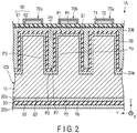
- FIG. 2 is a cross-sectional view taken along a line II-II of the capacitor shown in FIG. 1 .
- FIG. 3 is a cross-sectional view taken along a line III-III of the capacitor shown in FIG. 1 .
- FIG. 4 is a cross-sectional view taken along a line IV-IV of the capacitor shown in FIG. 1 .
- FIG. 5 is a cross-sectional view taken along a line V-V of the capacitor shown in FIG. 1 .
- FIG. 6 is a cross-sectional view taken along a line VI-VI of the capacitor shown in FIG. 1 .
- a capacitor 1A shown in FIG. 1 to 6 includes a substrate 10, a first conductive layer 20a, a second conductive layer 20b, and a dielectric layer 50, as shown in FIG. 2 to 6 .
- an X direction is a direction parallel to a main surface of the substrate 10
- a Y direction is a direction parallel to the main surface of the substrate 10 and perpendicular to the X direction.
- a Z direction is a thickness direction of the substrate 10, that is, a direction perpendicular to the X direction and the Y direction.
- the substrate 10 is, for example, an insulating substrate, a semiconductor substrate, or a conductive substrate.
- the substrate 10 is preferably a semiconductor substrate.
- the substrate 10 is preferably a substrate containing silicon, such as a silicon substrate. Such a substrate can be processed using a semiconductor process.
- the substrate 10 has a first main surface S1, and a second main surface S2 which is a back surface of the first main surface S1.
- the first main surface S1 and the second main surface S2 are a first surface and a second surface, respectively.
- the first main surface S1 is provided with first recesses R1 shown in FIG. 1 , 2 , and 4 to 6 .
- the first recesses R1 are first trenches each having a shape extending in the X direction.
- the first recesses R1 are arranged in the Y direction as shown in FIG. 1 , 2 , and 4 .
- a plurality of first recesses R1 may be provided on the first main surface S1, or only one first recess R1 may be provided.
- the second main surface S2 is provided with second recesses R2 shown in FIG. 1 , 3 , and 4 to 6 .
- these second recesses R2 are second trenches each having a shape extending in the Y direction.
- the second recesses R2 are arranged in the X direction as shown in FIG. 1 , 3 , and 5 .
- a plurality of second recesses R2 may be provided on the second main surface S2, or only one second recess R2 may be provided.
- a length direction of the first recesses R1 and a length direction of the second recesses R2 intersect each other.
- the length direction of the first recesses R1 and the length direction of the second recesses R2 are orthogonal to each other.
- the length direction of the first recesses R1 and the length direction of the second recesses R2 may intersect diagonally.
- the "length direction" of the first or second recesses is a length direction of orthogonal projections of the first or second recesses onto a plane perpendicular to the thickness direction of the substrate 10. Accordingly, the fact that the length direction of the first recesses R1 and the length direction of the second recesses R2 intersect each other means that the length direction of the orthogonal projections of the first recesses onto the plane perpendicular to the thickness direction of the substrate 10 intersects the length direction of the orthogonal projections of the second recesses onto this plane.
- a sum of a depth D1 of the first recesses R1 and a depth D2 of the second recesses R2, D1 + D2, is equal to or greater than a thickness T of the substrate 10. If this configuration is adopted, the first recesses R1 and the second recesses R2 are connected to each other at positions where they intersect to form first through holes TH1 shown in FIG. 6 .
- a ratio between the sum D1 + D2 and the thickness T, (D1 + D2)/T is preferably within a range of 1 to 1.4, and more preferably within a range of 1.1 to 1.3. From the viewpoint of increasing the electric capacity, the ratio (D1 + D2)/T is preferably large. In addition, from the viewpoint of improving an electrical connection between portions of the first conductive layer 20a or the second conductive layer 20b that are located on side walls and bottom surfaces of the first recesses R1 and portions of the first conductive layer 20a or the second conductive layer 20b that are located on side walls and bottom surfaces of the second recess R2, it is preferable that the ratio (D1 + D2)/T is large. However, when the depths D1 and D2 are increased, the mechanical strength of the capacitor 1A decreases.
- the ratio (D1 + D2)/T may be less than 1.
- the first recesses R1 and the second recesses R2 do not form the first through holes TH1 shown in FIG. 6 at the positions where they intersect. Therefore, in this case, in addition to providing the first recesses R1 and the second recesses R2, the first through holes are provided at any positions of the substrate 10. In this case, either or both of the first recesses R1 and the second recesses R2 can be omitted.
- a dimension of an opening of each of the first recess R1 and the second recess R2 is 0.3 ⁇ m or more.
- the dimensions of the openings of the first recesses R1 and the second recesses R2 are diameters or widths of the openings of the first recesses R1 and the second recesses R2.
- the dimension of the opening of each of the first recesses R1 and the second recesses R2 is a dimension in a direction perpendicular to the length direction thereof. When these dimensions are reduced, a larger electrical capacity can be achieved. However, if these dimensions are reduced, it becomes difficult to form a stacked structure including the first conductive layer 20a, the dielectric layer 50, and the second conductive layer 20b in the first recesses R1 and the second recesses R2 .
- a distance between adjacent first recesses R1 and a distance between adjacent second recesses R2 are preferably 0.1 ⁇ m or more. When these distances are reduced, a larger electric capacity can be achieved. However, if these distances are reduced, a portion of the substrate 10 sandwiched between the first recesses R1 and a portion of the substrate 10 sandwiched between the second recesses R2 are likely to be damaged.
- the first recesses R1 and the second recesses R2 can have various shapes.
- the first recesses R1 and the second recesses R2 may have a curved or bent shape, and may be circular or square, as long as their orthogonal projections onto a plane perpendicular to the Z direction intersect each other.
- cross sections of the first recesses R1 and the second recesses R2 parallel to the depth directions are rectangular. These cross sections may not be rectangular. For example, these cross sections may have a tapered shape.
- the first through holes TH1 are arranged corresponding to intersections of the first recesses R1 and the second recesses R2.
- Each of the first through holes TH1 is constituted by a part of the first recess R1 and a part of the second recess R2.
- Each of the first through holes TH1 extends from the first main surface S1 to the second main surface S2. That is, each of the first through holes TH1 extends in the Z direction, which is the thickness direction of the substrate 10.
- the first conductive layer 20a is provided on the substrate 10 as shown in FIG. 2 to 6 .
- the first conductive layer 20a and the substrate 10 constitute a conductive substrate CS.
- the first conductive layer 20a is made of polysilicon doped with impurities to improve conductivity, or a metal or alloy such as nickel or copper.
- the first conductive layer 20a may have a single-layer structure or a multi-layer structure.
- a thickness of the first conductive layer 20a is preferably within a range of 0.05 ⁇ m to 1 ⁇ m, and more preferably within a range of 0.1 ⁇ m to 0.3 ⁇ m. If the first conductive layer 20a is thin, there is a possibility that a discontinuous portion may be generated in the first conductive layer 20a, or a sheet resistance of the first conductive layer 20a may be excessively increased. When the first conductive layer 20a is thickened, it may be difficult to form a stacked structure of the first conductive layer 20a, the dielectric layer 50, and the second conductive layer 20b in the first recess R1 and the second recess R2.
- the first conductive layer 20a includes a first portion P1 shown in FIG. 2 to 4 and 6 , a second portion P2 shown in FIG. 2 , 3 , 5 , and 6 , third portions P3 shown in FIG. 2 and 4 to 6 , and fourth portions P4 shown in FIG. 3 to 6 .
- the first portion P1 is a portion of the first conductive layer 20a that is provided on the first main surface S1.
- the second portion P2 is a portion of the first conductive layer 20a that is provided on the second main surface S2.
- the third portions P3 are portions of the first conductive layer 20a that are provided on inner surfaces of the first recesses R1.
- the fourth portions P4 are portions of the first conductive layer 20a that are provided on inner surfaces of the second recesses R2.
- the first conductive layer 20a covers the first main surface S1, the second main surface S2, and the side walls of the first through holes TH1. Furthermore, the first conductive layer 20a covers the side walls and the bottom surfaces of the first recesses R1 and the side walls and the bottom surfaces of the second recesses R2.
- the first part P1 and the third parts P3 are electrically connected together, as can be seen from FIG. 2 , 4 , and 6 .
- the second portion P2 and the fourth portions P4 are also electrically connected together, as can be seen from FIG. 3 , 5 , and 6 .
- the third portions P3 and the fourth portions P4 are electrically connected together at the positions of the first through holes TH1 shown in FIG. 6 .
- the first conductive layer 20a may be a high-concentration doped layer that is a surface region of the silicon substrate doped with impurities at a high concentration.
- the first conductive layer 20a can be omitted.
- at least a surface region of the substrate 10, for example, the entire substrate 10 serves as the first conductive layer 20a.
- the second conductive layer 20b faces the first conductive layer 20a with the dielectric layer 50 interposed therebetween.
- the second conductive layer 20b is made of polysilicon doped with impurities to improve the conductivity, or a metal or alloy such as nickel or copper.
- the second conductive layer 20b may have a single-layer structure or a multi-layer structure.
- the thickness of the second conductive layer 20b is preferably within a range of 0.05 ⁇ m to 1 ⁇ m, and more preferably within a range of 0.1 ⁇ m to 0.3 ⁇ m. If the second conductive layer 20b is thin, there is a possibility that a discontinuous portion may be generated in the second conductive layer 20b, or a sheet resistance of the second conductive layer 20b may be excessively increased. If the second conductive layer 20b is thick, it may be difficult to form the first conductive layer 20a and the dielectric layer 50 with sufficient thicknesses.
- the second conductive layer 20b includes a fifth portion P5 shown in FIG. 2 to 4 and 6 , a sixth portion P6 shown in FIG. 2 , 3 , 5 , and 6 , seventh portions P7 shown in FIG. 2 and 4 to 6 , and eighth portions P8 shown in FIG. 3 to 6 .
- the fifth portion P5 is a portion of the second conductive layer 20b that faces the first main surface S1 with the first portion P1 interposed therebetween.
- the sixth portion P6 is a portion of the second conductive layer 20b that faces the second main surface S2 with the second portion P2 interposed therebetween.
- the seventh portions P7 are portions of the second conductive layer 20b that face the inner surfaces of the first recesses R1 with the third portions P3 interposed therebetween.
- the eighth portions P8 are portions of the second conductive layer 20b that face the inner surfaces of the second recesses R2 with the fourth portions P4 interposed therebetween.
- the second conductive layer 20b faces the first main surface S1, the second main surface S2, and the side walls of the first through holes TH1, with the first conductive layer 20a interposed therebetween. Furthermore, the second conductive layer 20b faces the side walls and the bottom surfaces of the first recesses R1 and the side walls and the bottom surfaces of the second recesses R2, with the first conductive layer 20a interposed therebetween.
- the fifth portion P5 and the seventh portions P7 are electrically connected together, as can be seen from FIG. 2 , 4 , and 6 .
- the sixth portion P6 and the eighth portions P8 are also electrically connected together, as can be seen from FIG. 3 , 5 , and 6 .
- the seventh portions P7 and the eighth portions P8 are electrically connected together at the positions of the first through holes TH1 shown in FIG. 6 .
- the second conductive layer 20b is provided so that the first recesses R1 and the second recesses R2 are completely filled with the first conductive layer 20a, the second conductive layer 20b, and the dielectric layer 50.
- the second conductive layer 20b may be a layer that is conformal to the first conductive layer 20a. That is, the second conductive layer 20b may be a layer having a substantially uniform thickness. In this case, the first recess R1 and the second recess R2 are not completely filled with the first conductive layer 20a, the second conductive layer 20b, and the dielectric layer 50.
- the second conductive layer 20b is provided with a plurality of through holes.
- these through holes are provided in a portion of the second conductive layer 20b that faces the first main surface with the first conductive layer 20a and the dielectric layer 50 interposed therebetween, at positions corresponding to the intersections of the first recesses R1 and the second recesses R2.
- the second conductive layer 20b may be provided with through holes at other positions. Further, the second conductive layer 20b may be provided with only one through hole.
- the dielectric layer 50 is interposed between the first conductive layer 20a and the second conductive layer 20b.
- the dielectric layer 50 is a layer that is conformal to the first conductive layer 20a.
- the dielectric layer 50 electrically insulates the first conductive layer 20a and the second conductive layer 20b from each other.
- the dielectric layer 50 is made of, for example, an inorganic dielectric.
- an inorganic dielectric a ferroelectric can also be used.
- Paraelectrics such as silicon nitride, silicon oxide, silicon oxynitride, titanium oxide, and tantalum oxide, are preferable. These paraelectrics have a small change in dielectric constant with temperature. Therefore, when the paraelectrics are used for the dielectric layer 50, the heat resistance of the capacitor 1A can be improved.
- a thickness of the dielectric layer 50 is preferably within a range of 0.005 ⁇ m to 0.5 ⁇ m, and more preferably within a range of 0.01 ⁇ m to 0.1 ⁇ m.
- the dielectric layer 50 is thin, there is a possibility that a discontinuous portion may be generated in the dielectric layer 50, and the first conductive layer 20a and the second conductive layer 20b may be short-circuited. Further, if the dielectric layer 50 is thinned, a withstand voltage is lowered even if there is no short circuit, and a possibility of short-circuiting when a voltage is applied is increased. When the dielectric layer 50 is thickened, the withstand voltage increases, but the electric capacity decreases.
- the dielectric layer 50 is provided with a plurality of through holes.
- the through holes of the dielectric layer 50 are connected to the through holes of the second conductive layer 20b.
- the capacitor 1A further includes an insulating layer 60 shown in FIG. 1 to 6 , electrodes 70a and 70b shown in FIG. 1 , 2 , 4 , and 6 , and pads 70c and 70d shown in FIG. 1 .
- the insulating layer 60 faces the first main surface S1 with a part of the first conductive layer 20a, a part of the second conductive layer 20b, and a part of the dielectric layer 50, interposed therebetween. Specifically, the insulating layer 60 covers the fifth portion P5 and the seventh portion P7 of the second conductive layer 20b.
- the insulating layer 60 includes a first insulating layer 61 and a second insulating layer 62.
- the first insulating layer 61 covers the fifth portion P5 and the seventh portion P7 of the second conductive layer 20b.
- the first insulating layer 61 further covers the side walls of the through holes provided in the second conductive layer 20b and the side walls of the through holes provided in the dielectric layer 50.
- the first insulating layer 61 is made of, for example, an inorganic insulator such as silicon nitride.
- the second insulating layer 62 covers the first insulating layer 61.
- the second insulating layer 62 is made of, for example, an organic insulator such as polyimide.
- the insulating layer 60 may have a multi-layer structure or a single-layer structure.
- the insulating layer 60 is provided with a plurality of through holes. Some of these through holes are connected to the through holes provided in the dielectric layer 50 via the through holes provided in the second conductive layer 20b, and together with them, form first contact holes. The rest of the through holes provided in the insulating layer 60 are provided at an intermediate position between the first contact holes adjacent in the Y direction to form second contact holes.
- the electrode 70a is provided on the insulating layer 60.
- the electrode 70a is a comb-shaped electrode.
- the electrode 70a has comb tooth portions each extending in the X direction and arranged in the Y direction.
- the comb tooth portions of the electrode 70b and the comb tooth portions of the electrode 70a are alternately arrayed in the Y direction.
- the electrode 70a is a second electrode.
- the electrode 70a fills the second contact holes.
- the electrode 70a is electrically connected to the second conductive layer 20b.
- the electrode 70a is the comb-shaped electrode herein, but the electrode 70a may have other shapes.
- the electrode 70b is provided on the insulating layer 60.
- the electrode 70b is a comb-shaped electrode.
- the electrode 70b has comb tooth portions each extending in the X direction and arranged in the Y direction.
- the electrode 70b is a first electrode.
- the electrode 70b fills the first contact holes.
- the electrode 70b is electrically connected to the first conductive layer 20a.
- the electrode 70b is the comb-shaped electrode herein, but the electrode 70b may have other shapes.
- the pad 70c is provided on the insulating layer 60.
- the pad 70c is electrically connected to the electrode 70a.
- the pad 70d is provided on the insulating layer 60.
- the pad 70d is electrically connected to the electrode 70b.
- the electrodes 70a and 70b and the pads 70c and 70d have a stacked structure including a barrier layer (not shown), a first metal layer 71, and a second metal layer 72.
- the barrier layer is made of, for example, titanium.
- the first metal layer 71 is provided on the barrier layer.
- the first metal layer 71 is made of, for example, copper.
- the second metal layer 72 covers an upper surface and an end surface of the first metal layer 71.
- the second metal layer 72 is constituted of, for example, a stacked film of a nickel or nickel alloy layer and a gold layer.
- the barrier layer and the second metal layer 72 can be omitted.
- This capacitor 1A is manufactured by, for example, the following method.
- FIG. 7 is a cross-sectional view schematically showing a first step of forming a catalyst layer in the manufacture of the capacitor shown in FIG. 1 to 6 .
- FIG. 8 is a cross-sectional view schematically showing a second step of forming a catalyst layer in the manufacture of the capacitor shown in FIG. 1 to 6 .
- FIG. 9 is a cross-sectional view schematically showing an etching step in the manufacture of the capacitor shown in FIG. 1 to 6 .
- FIG. 10 is another cross-sectional view schematically showing the etching step in the manufacture of the capacitor shown in FIG. 1 to 6 .
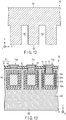
- FIG. 11 is a cross-sectional view schematically showing an example of a structure obtained by the etching step of FIG. 9 and 10 .
- FIG. 12 is another cross-sectional view of the structure shown in FIG. 11 .
- the substrate 10 shown in FIG. 7 is prepared.
- the substrate 10 is assumed to be a single-crystal silicon wafer.
- a plane orientation of the single-crystal silicon wafer is not particularly limited.
- a silicon wafer whose first main surface S1 is a (100) plane is used.
- a silicon wafer whose first main surface S1 is a (110) plane can also be used.
- the first through hole TH1 is formed on the substrate 10 by MacEtch (Metal-Assisted Chemical Etching).
- first catalyst layers 80a and 80b containing a first noble metal are first formed on the substrate 10.
- the first catalyst layers 80a and 80b are formed so as to partially cover the first main surface S1 and the second main surface S2, respectively.
- a first mask layer 90a is first formed on the first main surface S1 of the substrate 10.
- the first mask layer 90a is opened at positions corresponding to the first recesses R1.
- the first mask layer 90a prevents a portion of the first main surface S1 that is covered with the first mask layer 90a, from coming into contact with a noble metal to be described later.
- Examples of the material of the first mask layer 90a include organic materials such as polyimide, fluororesin, phenol resin, acrylic resin, and novolac resin, and inorganic materials such as silicon oxide and silicon nitride.
- the first mask layer 90a can be formed by, for example, existing semiconductor processes.
- the first mask layer 90a made of an organic material can be formed by, for example, photolithography.
- the first mask layer 90a made of an inorganic material can be formed by, for example, deposition of an inorganic material layer by vapor deposition, formation of a mask by photolithography, and patterning of the inorganic material layer by etching.
- the first mask layer 90a made of an inorganic material can be formed by oxidation or nitriding of the surface region of the substrate 10, formation of a mask by photolithography, and patterning of an oxide or nitride layer by etching.
- the first mask layer 90a can be omitted.
- the catalyst layer 80a is formed on each of the regions of the first main surface S1 that are not covered with the first mask layer 90a.
- the catalyst layer 80a is, for example, a discontinuous layer containing a noble metal.
- the catalyst layer 80a is a particulate layer made of catalyst particles 81a containing a noble metal.
- the noble metal is, for example, one or more of gold, silver, platinum, rhodium, palladium, and ruthenium.
- the catalyst layer 80a and the catalyst particles 81a may further contain a metal other than a noble metal, such as titanium.
- the catalyst layer 80a can be formed by, for example, electroplating, reduction plating, or displacement plating.
- the catalyst layer 80a can also be formed by application of a dispersion containing noble metal particles, or vapor deposition such as evaporation or sputtering.
- the displacement plating is particularly favorable because it is possible to directly and evenly deposit a noble metal on regions of the first main surface S1 that are not covered with the first mask layer 90a.
- a second mask layer 90b is formed on the second main surface S2 of the substrate 10.
- the second mask layer 90b is opened at positions corresponding to the second recesses R2.
- the second mask layer 90b prevents a portion of the second main surface S2 that is covered with the second mask layer 90b, from coming into contact with the noble metal.
- the material of the second mask layer 90b for example, those exemplified for the first mask layer 90a can be used.
- the second mask layer 90b can be formed, for example, by the same method as described above for the first mask layer 90a.
- a catalyst layer 80b is formed on each of the regions of the second main surface S2 that are not covered with the second mask layer 90b.
- the catalyst layer 80b is, for example, a discontinuous layer containing a noble metal.
- the catalyst layer 80b is assumed to be a particulate layer made of catalyst particles 81b containing a noble metal.
- the catalyst layer 80b and the catalyst particles 81b As materials for the catalyst layer 80b and the catalyst particles 81b, for example, those exemplified for the catalyst layer 80a and the catalyst particles 81a can be used.
- the catalyst layer 80b can be formed, for example, by the same method as described above for the catalyst layer 80a.
- the second mask layer 90b is formed on the second main surface S2, and subsequently, the catalyst layer 80a and the catalyst particles 81a are formed, and then the catalyst layer 80b and the catalyst particles 81b is formed. It is also possible that after forming the first mask layer 90a on the first main surface S1, the second mask layer 90b is formed on the second main surface S2, and after that, the substrate is immersed in a plating solution so that the catalyst layer 80a and the catalyst particles 81a, and the catalyst layer 80b and the catalyst particles 81b, are formed at the same time.
- the substrate 10 is etched with an assist from the noble metal as a catalyst to form the first through holes TH1 shown in FIG. 6 in the substrate 10.
- the substrate 10 is etched with an etching agent 100.
- the substrate 10 is immersed in the etching agent 100 in liquid form to bring the etching agent 100 into contact with the substrate 10.
- the etching agent 100 contains an oxidizing agent and hydrogen fluoride.
- the concentration of hydrogen fluoride in the etching agent 100 is preferably within a range of 1 mol/L to 20 mol/L, more preferably within a range of 5 mol/L to 10 mol/L, and further preferably within a range of 3 mol/L to 7 mol/L.
- the hydrogen fluoride concentration is low, it is difficult to achieve a high etching rate.
- the hydrogen fluoride concentration is high, excessive side etching may occur.
- the oxidizer can be selected from, for example, hydrogen peroxide, nitric acid, AgNO 3 , KAuCl 4 , HAuCl 4 , K 2 PtCl 6 , H 2 PtCl 6 , Fe(NO 3 ) 3 , Ni(NO 3 ) 2 , Mg(NO 3 ) 2 , Na 2 S 2 O 8 , K 2 S 2 O 8 , KMnO 4 , and K 2 Cr 2 O 7 .
- Hydrogen peroxide is favorable as the oxidizer because no harmful byproduct is produced and a semiconductor element is not contaminated.
- the concentration of the oxidizer in the etching agent 100 is preferably within a range of 0.2 mol/L to 8 mol/L, more preferably within a range of 2 mol/L to 4 mol/L, and further preferably within a range of 3 mol/L to 4 mol/L.
- the etching agent 100 may further contain a buffer.
- the buffer contains, for example, at least one of ammonium fluoride and ammonia.
- the buffer is ammonium fluoride.
- the buffer is a mixture of ammonium fluoride and ammonia.
- the etching agent 100 may further contain other components such as water.
- the material of the substrate 10, silicon herein is oxidized only in regions of the substrate 10 that are close to the first catalyst particles 81a or the second catalyst particles 82b. Oxide generated thereby is dissolved and removed by hydrofluoric acid. Therefore, only the portions close to the first catalyst particles 81a or the second catalyst particles 82b are selectively etched.
- the first catalyst particles 81a move toward the second main surface S2 with the progress of etching, where etching similar to the above is performed. As a result, as shown in FIG. 9 , at the position of the first catalyst layer 80a, etching proceeds from the first main surface S1 toward the second main surface S2 in a direction perpendicular to the first main surface S1.
- the second catalyst particles 81b move toward the first main surface S1 with the progress of etching, where etching similar to the above is performed.
- etching proceeds from the second main surface S2 toward the first main surface S1 in a direction perpendicular to the second main surface S2.
- the first recesses R1 are formed on the first main surface S1, and the second recesses R2 are formed on the second main surface S2.
- the first recesses R1 and the second recesses R2 are connected together at positions where they intersect to form the first through holes TH1 shown in FIG. 6 .
- first mask layer 90a and the second mask layer 90b, and the catalyst layers 80a and 80b are removed from the substrate 10.
- One or more of the first mask layer 90a, the second mask layer 90b, and the catalyst layers 80a and 80b may not be removed from the substrate 10.
- the first conductive layer 20a shown in FIG. 2 to 6 is formed on the substrate 10.
- the first conductive layer 20a is made of polysilicon
- such a layer can be formed by, for example, LPCVD (low pressure chemical vapor deposition).
- LPCVD low pressure chemical vapor deposition
- the first conductive layer 20a is made of metal
- such a layer can be formed by, for example, electrolytic plating, reduction plating, or displacement plating.
- a plating solution is a liquid containing a salt of a metal to be plated.
- a general plating solution such as a copper sulfate plating solution containing copper sulfate pentahydrate and sulfuric acid, a copper pyrophosphate plating solution containing copper pyrophosphate and potassium pyrophosphate, and a nickel sulfamate plating solution containing nickel sulfamate and boron, can be used.
- the first conductive layer 20a is preferably formed by a plating method using a plating solution containing a salt of a metal to be plated, a surfactant, and carbon dioxide in a supercritical or subcritical state.
- the surfactant is interposed between particles made of supercritical carbon dioxide and a continuous phase of a solution containing a salt of the metal to be plated. That is, the surfactant is allowed to form micelles in the plating solution, and supercritical carbon dioxide is incorporated in these micelles.
- the supply of the metal to be plated may be insufficient in the vicinity of the bottoms of the first recesses R1 and the second recesses R2. This is particularly noticeable when the ratio D1/W1 of the depth D1 to the width or diameter W1 of the first recess R1, or the ratio D2/W2 of the depth D2 to the width or diameter W2 of the second recess R2, is large.
- the micelles incorporating supercritical carbon dioxide can easily enter narrow gaps. As the micelles move, the solution containing the salt of the metal to be plated also moves. Therefore, according to a plating method using a plating solution containing a salt of a metal to be plated, a surfactant, and carbon dioxide in a supercritical or subcritical state, the first conductive layer 20a having a uniform thickness can be easily formed.
- the dielectric layer 50 is formed on the first conductive layer 20a.
- the dielectric layer 50 can be formed by, for example, CVD (chemical vapor deposition).
- the dielectric layer 50 can be formed by oxidizing, nitriding, or oxynitriding the surface of the first conductive layer 20a.
- the second conductive layer 20b is formed on the dielectric layer 50.
- the second conductive layer 20b can be formed, for example, by the same method as described above for the first conductive layer 20a.
- the second conductive layer 20b is also preferably formed by a plating method using a plating solution containing a salt of a metal to be plated, a surfactant, and carbon dioxide in a supercritical or subcritical state.
- a plurality of through holes are formed in a stacked body including the second conductive layer 20b and the dielectric layer 50.
- these through holes are formed in a portion of the stacked body that faces the first main surface with the first conductive layer 20a interposed therebetween, at positions corresponding to intersections of the first recesses R1 and the second recesses R2.
- These through holes can be formed by, for example, formation of a mask by photolithography and patterning by etching.
- the first insulating layer 61 is formed on the fifth portion P5 and the seventh portion P7 of the second conductive layer 20b.
- the first insulating layer 61 can be formed by, for example, CVD.
- the second insulating layer 62 is formed on the first insulating layer 61.
- the second insulating layer 62 is provided with through holes at the positions of the through holes provided in the above stacked body.
- the second insulating layer 62 having the through holes can be obtained using photolithography.
- the first insulating layer 61 is etched using the second insulating layer 62 as an etching mask. As a result, a portion of the first insulating layer 61 that covers the first conductive layer 20a is removed.
- the first metal layer 71 and the second metal layer 72 are formed in this order.
- the first metal layer 71 and the second metal layer 72 can be formed by, for example, a combination of film formation by sputtering or plating, and photolithography.
- this capacitor 1A the stacked structure including the first conductive layer 20a, the dielectric layer 50, and the second conductive layer 20b is provided not only on the first main surface S1, but also on the second main surface S2 and in the first through holes TH1. Therefore, this capacitor 1A can achieve a large electric capacity.
- the first recesses R1 and the second recesses R2 are trenches.
- the above stacked structure is also provided on the side walls and the bottom surfaces of the trenches. Therefore, this capacitor 1A can achieve a particularly large electric capacity.
- first recesses R1 and the second recesses R2 have a depth of 100 ⁇ m and a width of 1 ⁇ m, a distance between adjacent first recesses R1 and a distance between adjacent second recesses R2 are both 1 ⁇ m, and a silicon oxide film having a thickness of 0.02 ⁇ m is used as the dielectric layer 50, if the thickness of the capacitor 1A is assumed to be about 0.2 mm, a capacitance density of about 650 nF/mm 2 can be achieved.
- the first recesses R1 and the second recesses R2 intersect each other, and the sum D1 + D2 of their depths is equal to or greater than the thickness T of the substrate 10. Therefore, when the first recesses R1 and the second recesses R2 are formed, the first through holes TH1 are generated at the positions where they intersect. That is, unlike the case where the first recess R1 and the second recess R2 are merely formed on the first main surface S1 and the second main surface S2, respectively, such that the sum D1 + D2 is smaller than the thickness T, if the step of forming the first recess R1 and the second recess R2 is performed, there is no need to perform a step of forming the first through holes TH1.
- both electrodes 70a and 70b can be disposed on one side of the capacitor 1A. That is, unlike the case where the first recess R1 and the second recess R2 are merely formed on the first main surface S1 and the second main surface S2, respectively, such that the sum D1 + D2 is smaller than the thickness T, it is not necessary to form the electrodes 70a and 70b and wirings similar thereto on the second main surface S2, thus the number of steps can be greatly reduced. Furthermore, the capacitor 1A employing such a configuration can be easily mounted on a wiring board, etc.
- FIG. 13 is a cross-sectional view schematically showing a capacitor according to a second embodiment.
- a capacitor 1B shown in FIG. 13 is the same as the capacitor 1A according to the first embodiment except that the following configuration is adopted.
- the capacitor 1B includes a first dielectric layer 50a instead of the dielectric layer 50.
- the first dielectric layer 50a is the same as the dielectric layer 50 of the capacitor 1A according to the first embodiment.
- the second conductive layer 20b is a layer that is conformal to the first conductive layer 20a.
- the capacitor 1B further includes a second dielectric layer 50b and a third conductive layer 20c.
- the second dielectric layer 50b is provided on the second conductive layer 20b.
- the second dielectric layer 50b is a layer that is conformal to the first conductive layer 20a.
- the same configuration as that of the first dielectric layer 50a can be adopted.
- the third conductive layer 20c is provided on the second dielectric layer 50b.
- the third conductive layer 20c for example, a configuration similar to that of the second conductive layer 20b can be adopted.
- the electrodes 70a and 70b and the pads 70c and 70d shown in FIG. 1 are formed of a stacked body that includes a third metal layer 73 in addition to the first metal layer 71 and the second metal layer 72.
- the third metal layer 73 for example, the same configuration as that of the first metal layer 71 can be adopted.
- the electrode 70a is not in contact with the second conductive layer 20b, parts of comb tooth portions of the electrode 70a are in contact with the first conductive layer 20a, and other parts of the comb tooth portions are in contact with the third conductive layer 20c. That is, the first conductive layer 20a and the third conductive layer 20c are electrically connected to each other.
- the electrode 70b is not in contact with the first conductive layer 20a and the third conductive layer 20c, and comb tooth portions of the electrode 70b are in contact with the second conductive layer 20b. That is, in this capacitor 1B, the electrode 70a is a first electrode, and the electrode 70b is a second electrode.
- This capacitor 1B has the same effect as described above for the capacitor 1A.
- the first conductive layer 20a, the first dielectric layer 50a, the second conductive layer 20b, the second dielectric layer 50b, and the third conductive layer 20c form a stacked structure. That is, in this capacitor 1B, as compared with the capacitor 1A, more conductive layers are stacked with a dielectric layer interposed therebetween. Therefore, this capacitor 1B can achieve a larger electric capacity.
- first recesses R1 and the second recesses R2 have a depth of 100 ⁇ m and a width of 1 ⁇ m
- a distance between adjacent first recesses R1 and a distance between adjacent second recesses R2 are both 1 ⁇ m
- a silicon oxide film having a thickness of 0.02 ⁇ m is used as the first dielectric layer 50a and the second dielectric layer 50b
- a thickness of the capacitor 1B is assumed to be about 0.2 mm
- a capacitance density of about 1300 nF/mm 2 can be achieved.
- FIG. 14 is a cross-sectional view schematically showing a capacitor according to a third embodiment.
- FIG. 15 is a perspective view schematically showing a part of the capacitor shown in FIG. 14.
- FIG. 15 illustrates a structure in which the electrode 70b, the electrode 70a, the insulating layer 60, and the second conductive layer 20b are omitted from the capacitor 1C illustrated in FIG. 14 .
- the capacitor 1C shown in FIG. 14 is the same as the capacitor 1A according to the first embodiment except that the following configuration is adopted.
- the second recesses R2 are omitted. That is, the capacitor 1C does not have the first through holes TH1 shown in FIG. 6 .
- this capacitor 1C as shown in FIG. 15 , one or more portions of the substrate 10 each sandwiched between two adjacent ones of the first recesses R1 are provided with one or more second through holes TH2 that connect one of the two adjacent first recesses R1 and the other. That is, in this capacitor 1C, a side wall of the one of the two adjacent first recesses R1 corresponds to a first surface, and a side wall of the other one of the two adjacent first recesses R1 corresponds to a second surface.
- the stacked structure including the first conductive layer 20a, the dielectric layer 50, and the second conductive layer 20b is provided not only on the first main surface S1 and the side walls and the bottom surfaces of the first recesses R1, but also on the side walls of the second through holes TH2. That is, the first conductive layer 20a further covers the side walls of the second through holes TH2 in addition to the first main surface S1 and the side walls and the bottom surfaces of the first recesses R1.
- the second conductive layer 20b faces the side walls of the second through holes TH2 in addition to facing the first main surface S1 and the side walls and the bottom surfaces of the first recesses R1, with the first conductive layer 20a interposed therebetween.
- An average diameter of the second through holes TH2 is preferably 0.3 ⁇ m or more.
- An average diameter of the second through holes TH2 is preferably 0.3 ⁇ m or more.
- a larger number of second through holes TH2 can be disposed, and thus a larger electric capacity can be achieved.
- the diameter of the second through holes TH2 is reduced too much, there is a possibility that it may be difficult to form the stacked structure of the first conductive layer 20a, the dielectric layer 50, and the second conductive layer 20b in the second through holes TH2.
- a proportion of a total area of openings of the second through holes TH2 in an area of a side wall of the first recess R1, which is hereinafter referred to as an aperture ratio, is preferably within a range of 30% to 90%, and more preferably within a range of 50% to 90%.
- a ratio of the number of the second through holes TH2 provided on a side wall of the first recess R1 to an area of the side wall, which is hereinafter referred to as a hole density, is preferably within a range of 0.4/ ⁇ m 2 to 20/ ⁇ m 2 , and more preferably within a range of 2/ ⁇ m 2 to 8/ ⁇ m 2 .
- a distance between adjacent first recesses R1 is preferably 0.1 ⁇ m or more, and more preferably 2 ⁇ m or more. When this distance is increased, a larger electric capacity can be achieved. However, since a rate of increase in electric capacity with respect to this distance gradually decreases as the distance increases, it is not effective to excessively increase the above distance. If this distance is increased, there is a possibility that it may be difficult to form the stacked structure of the first conductive layer 20a, the dielectric layer 50, and the second conductive layer 20b in the second through holes TH2.
- the capacitor 1C is manufactured, for example, by the following method.
- FIG. 16 is a perspective view schematically showing an example of a substrate provided with trenches, used for manufacture of the capacitor shown in FIG. 14 .
- FIG. 17 is a perspective view schematically showing a catalyst layer forming step in the manufacture of the capacitor shown in FIG. 14 .
- FIG. 18 is a perspective view schematically showing an example of a structure obtained by an etching step in the manufacture of the capacitor shown in FIG. 14 .
- the substrate 10 provided with a plurality of first recesses R1 on the first main surface S1 is prepared.
- the first recesses R1 are, for example, formed by the MacEtch described with reference to FIG. 7 to 12 .
- the second through holes TH2 are formed on the substrate 10 by the MacEch.
- the catalyst particles 81a are deposited on the side walls of the first recesses R1.
- the catalyst particles 81a are deposited such that sufficiently large gaps are generated between the catalyst particles 81a.
- the catalyst particles 81a may be deposited on the bottom surfaces of the first recesses R1 and the first main surface, but do not necessarily have to be deposited thereon. Therefore, prior to the deposition of the catalyst particles 81a, a mask layer (not shown) may be formed so as to cover the bottom surfaces of the first recesses R1 and the first main surface.
- the substrate 10 is etched with an assist from the noble metal as a catalyst to form the second through holes TH2 shown in FIG. 18 on the substrate 10.
- the substrate 10 is etched with an etching agent.
- the substrate 10 is immersed in a liquid etching agent, and the etching agent is brought into contact with the substrate 10.
- the etching agent those described in the first embodiment can be used.
- this stacked structure constitutes a capacitor in each of the recesses formed on the side walls of the first recesses R1. Therefore, one or more of the recesses formed on the side walls of the first recesses R1 need not be through holes.
- the first conductive layer 20a, the dielectric layer 50, the second conductive layer 20b, the insulating layer 60, the electrodes 70a and 70b, etc. are formed by the same method as described in the first embodiment. In this way, the capacitor 1C is obtained.
- the first recesses R1 are provided, and the second through holes TH2 are provided on the side walls of the first recesses R1.
- the stacked structure of the first conductive layer 20a, the dielectric layer 50, and the second conductive layer 20b is provided not only on the first main surface S1 and the side walls and the bottom surfaces of the first recesses R1, but also on the side walls of the second through holes TH2. Therefore, the capacitor 1C can achieve a large electric capacity.
- a depth of the first recesses R1 is 100 ⁇ m, a width is 1 ⁇ m, a distance between adjacent first recesses R1 is 1 ⁇ m, an aperture ratio on the side walls of the first recesses R1 is 30%, a hole density is 2/ ⁇ m 2 , and a silicon oxide film having a thickness of 0.02 ⁇ m is used as the dielectric layer 50, if a thickness of the capacitor 1C is about 0.2 mm, a capacitance density of about 500 nF/mm 2 can be achieved.
- FIG. 19 is a perspective view schematically showing a part of the capacitor according to the fourth embodiment.
- the capacitor according to the fourth embodiment is the same as the capacitor 1A according to the first embodiment, except that the following configuration is adopted.
- one or more portions of the substrate 10 each sandwiched between two adjacent first recesses R1 are provided with one or more second through holes TH2 that connect one of the two adjacent first recesses R1 and the other. That is, in this capacitor, a side wall of the one of the two adjacent first recesses R1 corresponds to a first surface, and a side wall of the other one of the two adjacent first recesses R1 corresponds to a second surface.
- one or more portions of the substrate 10 each sandwiched between two adjacent second recesses R2 are provided with one or more third through holes TH3 that connect one of the two adjacent second recesses R2 and the other. That is, in this capacitor, a side wall of the one of the two adjacent second recesses R2 also corresponds to a first surface, and a side wall of the other one of the two adjacent second recesses R2 also corresponds to a second surface.
- the stacked structure including the first conductive layer 20a, the dielectric layer 50, and the second conductive layer 20b is provided not only on the first main surface S1, the second main surface S2, the side walls and the bottom surfaces of the first recesses R1, and the side walls and the bottom surfaces of the second recesses R2, but also on the side walls of the second through holes TH2 and the side walls of the third through holes TH3. That is, the first conductive layer 20a covers the side walls of the second through holes TH2 and the side walls of the third through holes TH3, in addition to the first main surface S1, the second main surface S2, the side walls and the bottom surfaces of the first recesses R1, and the side walls and the bottom surfaces of the second recesses R2.
- the second conductive layer 20b faces the side walls of the second through holes TH2 and the side walls of the third through holes TH3 in addition to facing the first main surface S1, the second main surface S2, and the side walls and the bottom surfaces of the first recesses R1, with the first conductive layer 20a interposed therebetween.
- An average diameter of the second through holes TH2 and an average diameter of the third through holes TH3 are preferably within the range described for the second through holes TH2 in the third embodiment.
- a proportion of a total area of openings of the second through holes TH2 in an area of a side wall of the first recess R1 is preferably within the range of the aperture ratio described for the side walls of the first recesses R1 in the third embodiment. Further, a proportion of a total area of openings of the third through holes TH3 in an area of a side wall of the second recess R2 is also preferably within the range of the aperture ratio described for the side walls of the first recesses R1 in the third embodiment.
- a ratio of the number of the second through holes TH2 provided on a side wall of the first recess R1 to an area of the side wall is preferably within the range of the hole density described in the third embodiment. Further, a ratio of the number of third through holes TH3 provided on a side wall of the second recess R2 to an area of the side wall is preferably within the range of the hole density described in the third embodiment.
- a distance between adjacent first recesses R1 and a distance between adjacent second recesses R2 are preferably within the range described for the distance between the adjacent first recesses R1 in the third embodiment.
- the capacitor according to the fourth embodiment can be obtained, for example, by further performing a step for forming the second through holes TH2 and the third through holes TH3 in the manufacture of the capacitor 1A according to the first embodiment.
- the second through holes TH2 and the third through holes TH3 can be formed, for example, by the method described in the third embodiment.
- first recesses R1 are formed on the first main surface S1 of the substrate 10
- second recesses R2 are formed on the second main surface S2 of the substrate 10.
- the first recesses R1 and the second recesses R2 are formed, for example, by the MacEtch described in the first embodiment.
- a second catalyst layer containing a second noble metal is formed on the substrate 10 so as to partially cover the side walls of the first recesses R1 and the side walls of the second recesses R2.
- the substrate 10 is etched with an assist from the second noble metal as a catalyst so as to form the second through holes TH2 in one or more portions of the substrate 10 each sandwiched between two adjacent ones of the first recesses R1 and form the third through holes TH3 in one or more portions of the substrate 10 each sandwiched between two adjacent ones of the second recesses R2.
- a hole having a smaller diameter than a preferred diameter or a non-through hole may be formed. These holes are then embedded by any of the first conductive layer 20a, the dielectric layer 50, and the second conductive layer 20b, or at these positions, the first conductive layer 20a, the dielectric layer 50, and the second conductive layer 20b are formed conformally.
- the first conductive layer 20a, the dielectric layer 50, the second conductive layer 20b, the insulating layer 60, the electrodes 70a and 70b, etc. are formed by the same method as described in the first embodiment. In this way, the capacitor according to the fourth embodiment is obtained.
- the first recesses R1 and the second recesses R2 are provided, and the second through holes TH2 and the third through holes TH3 are provided on the side walls of the first recesses R1 and the side walls of the second recesses R2, respectively.
- the stacked structure of the first conductive layer 20a, the dielectric layer 50, and the second conductive layer 20b is provided not only on the first main surface S1, the second main surface S2, the side walls and the bottom surfaces of the first recesses R1, and the side walls and the bottom surfaces of the second recesses R2, but also on the side walls of the second through holes TH2 and the side walls of the third through holes TH3. Therefore, the capacitor 1C can achieve a large electric capacity.
- the first recesses R1 and the second recesses R2 are trenches.
- the above stacked structure is also provided on the side walls and the bottom surfaces of the trenches. Therefore, this capacitor can achieve a particularly large electric capacity.
- each of the side walls of the first recesses R1 and the second recesses provided with the second through holes TH2 and the third through holes TH3, respectively, has an aperture ratio of 30% and a hole density of 2/ ⁇ m 2 , and a silicon oxide film having a thickness of 0.02 ⁇ m is used as the dielectric layer 50, if a thickness of the capacitor is assumed to be about 0.2 mm, a capacitance density of about 1000 nF/mm 2 can be achieved.
- the first recesses R1 and the second recesses R2 intersect each other, and the sum D1 + D2 of their depths is equal to or greater than the thickness T of the substrate 10. Therefore, when the first recesses R1 and the second recesses R2 are formed, the first through holes TH1 are generated at the positions where they intersect. That is, unlike the case where the first recesses R1 and the second recesses R2 whose sum D1 + D2 is smaller than the thickness T are merely formed on the first main surface S1 and the second main surface S2, respectively, there is no need to further perform a step of forming the first through holes TH1 in addition to the step of forming the first recesses R1 and the second recesses R2.
- both electrodes 70a and 70b shown in FIG. 1 can be disposed on one side of the capacitor. That is, unlike the case where the first recesses R1 and the second recesses R2 are merely formed on the first main surface S1 and the second main surface S2, respectively, such that the sum D1 + D2 is smaller than the thickness T, it is not necessary to form the electrodes 70a and 70b or wirings similar thereto on the second main surface S2, thus the number of steps can be greatly reduced. Furthermore, a capacitor adopting such a configuration can be easily mounted on a wiring board, etc.
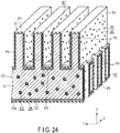
- FIG. 20 is a cross-sectional view schematically showing a capacitor according to a fifth embodiment.
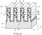
- FIG. 21 is a perspective view schematically showing a part of the capacitor shown in FIG. 20 .
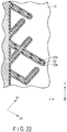
- FIG. 22 is a cross-sectional view taken along a line XXII-XXII of the capacitor shown in FIG. 21.
- FIG. 21 illustrates a structure of the capacitor 1D illustrated in FIG. 20 , from which the electrode 70b, the electrode 70a, the insulating layer 60, and the second conductive layer 20b are omitted.
- the capacitor 1D shown in FIG. 20 is the same as the capacitor 1C according to the third embodiment except that the following configuration is adopted.
- a plurality of first holes H1 and a plurality of second holes H2 are provided on the side walls of the first recesses R1, instead of the plurality of second through holes TH2.
- each of the first holes H1 extends in a first direction D1 inclined with respect to the side wall of the first recess R1. That is, length directions or depth directions of the first holes H1 are parallel to each other, and are inclined with respect to the side walls of the first recesses R1.
- Each of the first holes H1 may be a blind hole that extends from one of two adjacent ones of two or more first recesses R1, and does not reach the other.
- each of the first holes H1 may be a through hole that connects the two adjacent ones of the two or more first recesses R1 to each other.
- one or more of the first holes H1 may be blind holes, and the rest of the first holes H1 may be through holes.
- Each of the second holes H2 extends in a second direction D2 that intersects the first direction D1. That is, length directions or depth directions of the second holes H2 are parallel to each other, and are inclined with respect to the side walls of the first recesses R1. Each of the second holes H2 may or may not be connected to one or more of the first holes H1. Each of the second holes H2 may or may not intersect one or more of the first holes H1.
- Each of the second holes H2 may be a blind hole that extends from one of two adjacent ones of two or more first recesses R1 and does not reach the other.
- each of the second holes H2 may be a through hole that connects the two adjacent ones of the two or more first recesses R1 to each other.
- one or more of the second holes H2 may be blind holes, and the rest of the second holes H2 may be through holes.
- the stacked structure including the first conductive layer 20a, the dielectric layer 50, and the second conductive layer 20b is provided not only on the first main surface S1 and the side walls and the bottom surfaces of the first recesses R1, but also on side walls of the first holes H1 and side walls of the second holes H2. That is, the first conductive layer 20a further covers the side walls of the first holes H1 and the side walls of the second holes H2 in addition to the first main surface S1 and the side walls and the bottom surfaces of the first recesses R1.
- the second conductive layer 20b further faces the side walls of the first holes H1 and the side walls of the second holes H2 in addition to facing the first main surface S1 and the side walls and the bottom surfaces of the first recesses R1, with the first conductive layer 20a interposed therebetween.
- the first holes H1 are provided on the side walls of the first recesses R1.
- the substrate 10 of the capacitor 1D has a larger surface area than a substrate in which no hole is provided on the side walls of the first recesses R1.
- Each of the first holes H1 extends in the first direction D1 inclined with respect to the side walls of the first recesses R1. Therefore, the substrate 10 of the capacitor 1D has a larger surface area than a substrate in which holes extending in a direction perpendicular to the side walls of the first recesses R1 are provided on the side walls of the first recesses R1.
- the stacked structure of the first conductive layer 20a, the dielectric layer 50, and the second conductive layer 20b is provided not only on the first main surface S1 and the side walls and the bottom surfaces of the first recesses R1, but also on the side walls of the first holes H1.
- this capacitor 1D can achieve a larger electric capacity than a capacitor in which no hole is provided on the side walls of the first recesses R1. Further, this capacitor 1D can achieve a larger electric capacity than a capacitor provided with holes extending in a direction perpendicular to the side walls of the first recess R1.
- a surface area of the first conductive layer 20a when an angle formed by the first direction D1 with respect to the side walls of the first recesses R1 is 45° can be about 1.36 times the surface area of the first conductive layer 20a when this angle is 90°.
- a capacitor in which the first direction D1 is inclined with respect to the side walls of the first recesses R1 can achieve a larger electric capacity than a capacitor in which the first direction D1 is perpendicular to the side walls of the first recesses R1.
- the second holes H2 are further provided on the side walls of the first recesses R1. If the second holes H2 are provided in addition to the first holes H1, a larger electric capacity can be achieved.
- the first holes H1 are parallel to each other in the length direction, and the second holes H2 are also parallel to each other in the length direction.
- degradation in mechanical strength due to a connection between the first holes H1 or a connection between the second holes H2 less likely occurs.
- the angle formed by the first direction D1 with respect to the side walls of the first recesses R1 and the angle formed by the second direction D2 with respect to the side walls of the first recesses R1 are preferably within a range of 10° to 80°, and more preferably within a range of 30° to 60°. When this angle is reduced, the mechanical strength of the capacitor 1D is lowered. When this angle is increased, an increase in electric capacity associated with tilting the first direction D1 or the second direction D2 is reduced.
- the angle formed by the first direction D1 and the second direction D2 is preferably within a range of 20° to 160°, and more preferably within a range of 60° to 120°.
- the first direction D1 and the second direction D2 are particularly preferably orthogonal. When this angle is excessively decreased or increased, the mechanical strength of the capacitor 1D is lowered.
- first holes H1 and the second holes H2 in addition to the first holes H1 and the second holes H2, other holes each extending in one direction and whose length directions are different from the first direction D1 and the second direction D2, may further be provided.
- a plurality of holes whose length directions are parallel to each other and intersecting the first direction D1 and the second direction D2 and a plurality of holes whose length directions are parallel to each other and intersecting the first direction D1, the second direction D2, and the length directions of the previous holes may further be provided.
- FIG. 23 is a photomicrograph showing a cross section of the capacitor shown in FIG. 21 .
- the micrograph in FIG. 23 is a micrograph of the cross section corresponding to FIG. 22 .
- a vertical direction is the X direction
- a horizontal direction is the Y direction.
- the micrograph of FIG. 23 shows a cross section parallel to a (001) plane of a single-crystal silicon wafer having the (001) plane as a main surface and provided with a first recess R1 whose length direction is parallel to a ⁇ 100> axis on the previous main surface.
- the first direction D1 and the second direction D2 described above are directions parallel to a ⁇ 110> axis and a ⁇ -110> axis in FIG. 23 , respectively.
- the structure in which the first direction D1 and the second direction D2 are orthogonal to each other as shown is particularly advantageous in achieving a large electric capacity and a high mechanical strength.
- Each of an average diameter of the first holes H1 and an average diameter of the second holes H2 is preferably within the range described for the second through holes TH2 in the third embodiment.
- the diameter of the first hole H1 and the diameter of the second hole H2 are reduced, more first holes H1 and second holes H2 can be arranged, thereby achieving a larger electric capacity.
- the diameter of the first hole H1 and the diameter of the second hole H2 are reduced too much, there is a possibility that it may be difficult to form the stacked structure of the first conductive layer 20a, the dielectric layer 50, and the second conductive layer 20b in the first holes H1 and the second holes H2.
- a proportion of a sum of a total area of openings of the first holes H1 and a total area of openings of the second holes H2 in an area of a side wall of the first recess R1, which is hereinafter referred to as an aperture ratio, is preferably within the range of the aperture ratio described for the side walls of the first recesses R1 in the third embodiment.
- a ratio of the total number of the first holes H1 and the second holes H2 provided on a side wall of the first recess R1 to an area of the side wall which is hereinafter referred to as a hole density, is preferably within the range of the hole density described in the third embodiment.
- the second holes H2 may be omitted.
- Portions of the substrate 10 that are adjacent to the first recesses R1 are preferably made of crystal having a face-centered cubic structure.
- the main surface of the substrate 10 is preferably the (001) plane.
- the length directions of the first recesses R1 are preferably inclined with respect to the ⁇ 110> axis.
- the first holes H1 and the second holes H2 can be formed by a method to be described below.
- a single-crystal silicon wafer is used as the substrate 10 made of crystal having a face-centered cubic structure and having the (001) plane as the main surface.
- the first recesses R1 whose length directions are inclined with respect to the ⁇ 110> axis are formed on the main surface of the substrate 10.
- the first recesses R1 whose length directions are parallel to the ⁇ 100> axis are formed.
- the first recesses R1 can be formed, for example, by the method described with reference to FIG. 7 to 12 .
- catalyst particles are deposited on the side walls of the first recesses R1.
- the catalyst particles can be deposited, for example, by the method described with reference to FIG. 17 .
- the substrate 10 is etched with an assist from a noble metal as a catalyst to form the first holes H1 and the second holes H2.
- the substrate 10 is immersed in an etching agent, and the etching agent is brought into contact with the substrate 10.
- the etching agent those described in the first embodiment can be used.
- the etching proceeds in the thickness direction of a catalyst layer.
- the orientation of the crystal constituting the substrate has an influence on the etching progress direction.
- the etching is likely to proceed in a direction parallel to the ⁇ 110> axis or its equivalent, e.g., the ⁇ -110> axis.
- FIG. 24 is a perspective view schematically showing a part of the capacitor according to a sixth embodiment.
- the capacitor according to the sixth embodiment is the same as the capacitor according to the fourth embodiment except that the following configuration is adopted.
- a plurality of first holes H1 and a plurality of second holes H2 are provided on the side walls of the first recesses R1, instead of the plurality of second through holes TH2. Further, a plurality of third holes H3 and a plurality of fourth holes H4 are provided on the side walls of the second recesses R2, instead of the plurality of third through holes TH3.
- the first holes H1 and the second holes H2 in this capacitor are the same as the first holes H1 and the second holes H2 of the capacitor 1D according to the fifth embodiment.
- Each of the third holes H3 extends in a third direction inclined with respect to the side walls of the second recesses R2. That is, length directions or depth directions of the third holes H3 are parallel to each other, and are inclined with respect to the side walls of the second recesses R2.
- Each of the third holes H3 may be a blind hole that extends from one of two adjacent ones of two or more second recesses R2 and does not reach the other.
- each of the third holes H3 may be a through hole that connects the two adjacent ones of the two or more second recesses R2 to each other.
- one or more of the third holes H3 may be blind holes, and the rest of the third holes H3 may be through holes.
- Each of the fourth holes H4 extends in a fourth direction that intersects the third direction. That is, length directions or depth directions of the fourth holes H4 are parallel to each other, and inclined with respect to the side walls of the second recesses R2. Each of the fourth holes H4 may or may not be connected to one or more of the third holes H3. Eeach of the fourth holes H4 may or may not intersect one or more of the third holes H3.
- Each of the fourth holes H4 may be a blind hole that extends from one of the two adjacent ones of the two or more second recesses R2 and does not reach the other.
- each of the fourth holes H4 may be a through hole that connects the two adjacent ones of the two or more second recesses R2 to each other.
- one or more of the fourth holes H4 may be blind holes, and the rest of the fourth holes H4 may be through holes.
- the stacked structure including the first conductive layer 20a, the dielectric layer 50, and the second conductive layer 20b is provided not only on the first main surface S1, the second main surface S2, the side walls and the bottom surfaces of the first recesses R1, and the side walls and the bottom surfaces of the second recesses R2, but also on side walls of the first holes H1, side walls of the second holes H2, side walls of the third holes H3, and side walls of the fourth holes H4.
- the first conductive layer 20a further covers the side walls of the first holes H1, the side walls of the second holes H2, the side walls of the third holes H3, and the side walls of the fourth holes H4, in addition to the first main surface S1, the second main surface S2, the side walls and the bottom surfaces of the first recesses R1, and the side walls and the bottom surfaces of the second recesses R2.
- the second conductive layer 20b further faces the side walls of the first holes H1, the side walls of the second holes H2, the side walls of the third holes H3, and the side walls of the fourth holes H4, in addition to facing the first main surface S1, the second main surface S2, and the side walls and the bottom surfaces of the first recesses R1, with the first conductive layer 20a interposed therebetween.
- this capacitor is the same as the capacitor according to the fourth embodiment, except that the first holes H1 and the second holes H2 are provided instead of the second through holes TH2, and the third holes H3 and the fourth holes H4 are provided instead of the third through holes TH3. Therefore, this capacitor has the same effects as the capacitor according to the fourth embodiment except for the matters described in association with the second through holes TH2 and the third through holes TH3.
- the substrate 10 of this capacitor has a larger surface area than that of a substrate in which no hole is provided on any of the side walls of the first recesses R1 and the second recesses R2.
- the substrate 10 of this capacitor has a surface area larger than that of a substrate in which the side walls of the first recesses R1 are provided with holes extending in a direction perpendicular to these side walls, and the side walls of the second recesses R2 are provided with holes extending in a direction perpendicular to these side walls.
- the stacked structure of the first conductive layer 20a, the dielectric layer 50, and the second conductive layer 20b is provided not only on the first main surface S1, the second main surface S2, the side walls and the bottom surfaces of the first recesses R1, and the side walls and the bottom surfaces of the second recesses R2, but also on the side walls of the first holes H1, the second holes H2, the third holes H3, and the fourth holes H4.
- this capacitor can achieve a larger electric capacity than a capacitor in which no hole is provided on any of the side walls of the first recesses R1 and the second recesses R2.
- this capacitor can achieve a larger electric capacity than a capacitor in which the side walls of the first recesses R1 are provided with holes extending in a direction perpendicular to the side walls, and the side walls of the second recesses R2 are provided with holes extending in a direction perpendicular to the side walls.
- Each of an angle formed by the first direction D1 with respect to the side walls of the first recesses R1, an angle formed by the second direction D2 with respect to the side walls of the first recesses R1, an angle formed by the third direction with respect to the side walls of the second recesses R2, and an angle formed by the fourth direction with respect to the side walls of the second recesses R2 is preferably within the range described for the angle formed by the first direction D1 and the second direction D2 with respect to the side walls of the first recesses R1 in the fifth embodiment.
- Each of an angle formed by the first direction D1 and the second direction D2 and an angle formed by the third direction and the fourth direction is preferably within the range described for the angle formed by the first direction D1 and the second direction D2 in the fifth embodiment.
- one of the first direction D1 and the second direction D2 and one of the third direction and the fourth direction are parallel or orthogonal. In this case, formation of the holes is easy.
- Each of an average diameter of the first hole H1, an average diameter of the second holes H2, an average diameter of the third holes H3, and an average diameter of the fourth holes H4 is preferably within the range described for the second through holes TH2 in the third embodiment.
- An aperture ratio of a side wall of the first recess R1 i.e., a proportion of a sum of a total area of openings of the first holes H1 and a total area of openings of the second holes H2 in an area of this side wall is preferably within the range of the aperture ratio described for the side walls of the first recesses R1 in the third embodiment.
- an aperture ratio of a side wall of the second recess R2 i.e., a proportion of a sum of a total area of openings of the third holes H3 and a total area of openings of the fourth holes H4 in an area of this side wall, is also preferably within the range of the aperture ratio described for the side walls of the first recesses R1 in the third embodiment.
- a hole density in a side wall of the first recess R1 i.e., a ratio of the total number of the first holes H1 and the second holes H2 provided on this side wall to an area of the side wall is preferably within the range of the hole density described in the third embodiment.
- a hole density in a side wall of the second recess R2, i.e., a ratio of the total number of the third holes H3 and the fourth holes H4 provided on this side wall to an area of the side wall is also preferably within the range of the hole density described in the third embodiment.
- the rest may be omitted.
- portions adjacent to the first recesses R1 and portions adjacent to the second recesses R2 are preferably made of crystal having a face-centered cubic structure.
- the first main surface S1 is the (001) plane
- the second main surface S2 is a plane parallel to the first main surface S1.
- the length directions of the first recesses R1 and the second recesses R2 are inclined with respect to the ⁇ 110> axis.
- a single-crystal silicon wafer is used as the substrate 10 made of crystal having a face-centered cubic structure, in which the first main surface S1 is the (001) plane, and the second main surface S2 is parallel to the first main surface S1.
- the first recesses R1 whose length directions are inclined with respect to the ⁇ 110> axis are formed on the first main surface S1 of the substrate 10, and the second recesses R2 whose length directions are inclined with respect to the ⁇ 110> axis are formed on the second main surface S2 of the substrate 10.
- the first recesses R1 and the second recesses R2 are formed, for example, by the MacEtch described in the first embodiment.
- a second catalyst layer containing a second noble metal is formed on the substrate 10 so as to partially cover the side walls of the first recesses R1 and the side walls of the second recesses R2.
- the substrate 10 is etched with an assist from the second noble metal as a catalyst to form the first holes H1 and the second holes H2 on the side walls of the first recesses R1, and form the third holes H3 and the fourth holes H4 on the side walls of the second recesses R2.
- the orientation of the crystal constituting the substrate has an influence on the etching progress direction.
- the etching is likely to proceed in a direction parallel to the ⁇ 110> axis or its equivalent, e.g., the ⁇ -110> axis. Accordingly, according to the method described above, the structure shown in FIG. 24 is obtained.
- the capacitors according to the third to sixth embodiments may include a stacked structure of first conductive layer 20a, the first dielectric layer 50a, the second conductive layer 20b, the second dielectric layer 50b, and the third conductive layer 20c, instead of the stacked structure of the first conductive layer 20a, the dielectric layer 50, and the second conductive layer 20b.
- the second through holes TH2 or the third through holes TH3 may be omitted from the capacitor according to the fourth embodiment.
Landscapes
- Engineering & Computer Science (AREA)
- Power Engineering (AREA)
- Microelectronics & Electronic Packaging (AREA)
- Manufacturing & Machinery (AREA)
- Semiconductor Integrated Circuits (AREA)
- Fixed Capacitors And Capacitor Manufacturing Machines (AREA)
- Weting (AREA)
Abstract
Description
- Embodiments described herein relate generally to a capacitor and a manufacturing method thereof.
- Many electrical and electronic devices include capacitors. Such a capacitor can be obtained, for example, by forming conductive layers and a dielectric layer on a silicon substrate (see Jpn. Pat. Appln. KOKAI Publication No.
8-213565 - The problem to be solved by the present invention is to provide a capacitor capable of achieving a large electric capacity.
- According to a first aspect, there is provided a capacitor comprising: a substrate having a first surface and a second surface and provided with one or more first through holes each extending from the first surface to the second surface; a first conductive layer covering the first surface, the second surface, and side walls of the one or more first through holes; a second conductive layer facing the first surface, the second surface, and the side walls of the one or more first through holes, with the first conductive layer interposed therebetween; and a dielectric layer interposed between the first conductive layer and the second conductive layer.
- According to a second aspect, there is provided a capacitor comprising: a substrate having a first main surface and a second main surface, wherein a plurality of trenches are provided on the first main surface, and one or more portions each sandwiched between two adjacent ones of the plurality of trenches are provided with one or more through holes connecting one of the two adjacent trenches to the other; a first conductive layer covering the first main surface, side walls and bottom surfaces of the trenches, and side walls of the one or more through holes; a second conductive layer facing the first main surface, the side walls and the bottom surfaces of the trenches, and the side walls of the one or more through holes, with the first conductive layer interposed therebetween; and a dielectric layer interposed between the first conductive layer and the second conductive layer.
- According to a third aspect, there is provided a method of manufacturing a capacitor, comprising: forming a first catalyst layer containing a first noble metal on a substrate such that a surface of the substrate is covered partially; etching the substrate with an assist from the first noble metal as a catalyst to form one or more first through holes in the substrate; forming a first conductive layer on the substrate in which the one or more first through holes are formed; forming a dielectric layer on the first conductive layer; and forming a second conductive layer on the dielectric layer.
- According to a fourth aspect, there is provided a capacitor comprising: a substrate having a first main surface and a second main surface, wherein one or more first trenches are provided on the first main surface, and a plurality of first holes each extending in a first direction inclined with respect to side walls of the first trenches are provided on the side walls of the one or more first trenches; a first conductive layer covering the first main surface, the side walls and bottom surfaces of the first trenches, and side walls of the plurality of first holes; a second conductive layer facing the first main surface, the side walls and the bottom surfaces of the first trenches, and the side walls of the plurality of first holes, with the first conductive layer interposed therebetween; and a dielectric layer interposed between the first conductive layer and the second conductive layer.
- According to a fifth aspect, there is provided a method of manufacturing a capacitor, comprising: forming one or more first trenches on a first main surface of a substrate having the first main surface and a second main surface; forming a first catalyst layer containing a first noble metal on side walls of the one or more first trenches such that the side walls of the one or more first trenches are covered partially; etching the side walls of the first trenches with an assist from the first noble metal as a catalyst to form a plurality of first holes on the side walls of the first trenches, each of the first holes extending in a first direction inclined with respect to the side walls of the first trenches; forming a first conductive layer on the substrate on which the plurality of first holes are formed; forming a dielectric layer on the first conductive layer; and forming a second conductive layer on the dielectric layer.
-
-
FIG. 1 is a plan view schematically showing a capacitor according to a first embodiment; -
FIG. 2 is a cross-sectional view of the capacitor shown inFIG. 1 ; -
FIG. 3 is another cross-sectional view of the capacitor shown inFIG. 1 ; -
FIG. 4 is still another cross-sectional view of the capacitor shown inFIG. 1 ; -
FIG. 5 is still another cross-sectional view of the capacitor shown inFIG. 1 ; -
FIG. 6 is still another cross-sectional view of the capacitor shown inFIG. 1 ; -
FIG. 7 is a cross-sectional view schematically showing one process in the manufacture of the capacitor shown inFIG. 1 to 6 ; -
FIG. 8 is a cross-sectional view schematically showing another process in the manufacture of the capacitor shown inFIG. 1 to 6 ; -
FIG. 9 is a cross-sectional view schematically showing still another process in the manufacture of the capacitor shown inFIG. 1 to 6 ; -
FIG. 10 is another cross-sectional view schematically showing the process ofFIG. 9 ; -
FIG. 11 is a cross-sectional view schematically showing an example of a structure obtained by the processes ofFIG. 9 and10 ; -
FIG. 12 is another cross-sectional view of the structure shown inFIG. 11 ; -
FIG. 13 is a cross-sectional view schematically showing a capacitor according to a second embodiment; -
FIG. 14 is a cross-sectional view schematically showing a capacitor according to a third embodiment; -
FIG. 15 is a perspective view schematically showing a part of the capacitor shown inFIG. 14 ; -
FIG. 16 is a perspective view schematically showing an example of a substrate provided with trenches that is used for the manufacture of the capacitor shown inFIG. 14 ; -
FIG. 17 is a perspective view schematically showing one process in the manufacture of the capacitor shown inFIG. 14 ; -
FIG. 18 is a perspective view schematically showing an example of a structure obtained by another process in the manufacture of the capacitor shown inFIG. 14 ; -
FIG. 19 is a perspective view schematically showing a part of a capacitor according to a fourth embodiment; -
FIG. 20 is a cross-sectional view schematically showing a capacitor according to a fifth embodiment; -
FIG. 21 is a perspective view schematically showing a part of the capacitor shown inFIG. 20 ; -
FIG. 22 is a cross-sectional view taken along a line XXII-XXII of the capacitor shown inFIG. 21 ; -
FIG. 23 is a micrograph showing a cross section of the capacitor shown inFIG. 21 ; and -
FIG. 24 is a perspective view schematically showing a part of a capacitor according to a sixth embodiment. - Embodiments will be explained in detail below with reference to the accompanying drawings. Note that the same reference numerals denote constituent elements which achieve the same or similar functions throughout all the drawings, and a repetitive explanation will be omitted.
-
FIG. 1 is a plan view schematically showing a capacitor according to a first embodiment.FIG. 2 is a cross-sectional view taken along a line II-II of the capacitor shown inFIG. 1 .FIG. 3 is a cross-sectional view taken along a line III-III of the capacitor shown inFIG. 1 .FIG. 4 is a cross-sectional view taken along a line IV-IV of the capacitor shown inFIG. 1 .FIG. 5 is a cross-sectional view taken along a line V-V of the capacitor shown inFIG. 1 .FIG. 6 is a cross-sectional view taken along a line VI-VI of the capacitor shown inFIG. 1 . - A
capacitor 1A shown inFIG. 1 to 6 includes asubstrate 10, a firstconductive layer 20a, a secondconductive layer 20b, and adielectric layer 50, as shown inFIG. 2 to 6 . - In each figure, an X direction is a direction parallel to a main surface of the
substrate 10, and a Y direction is a direction parallel to the main surface of thesubstrate 10 and perpendicular to the X direction. A Z direction is a thickness direction of thesubstrate 10, that is, a direction perpendicular to the X direction and the Y direction. - The
substrate 10 is, for example, an insulating substrate, a semiconductor substrate, or a conductive substrate. Thesubstrate 10 is preferably a semiconductor substrate. Thesubstrate 10 is preferably a substrate containing silicon, such as a silicon substrate. Such a substrate can be processed using a semiconductor process. - As shown in
FIG. 2 to 6 , thesubstrate 10 has a first main surface S1, and a second main surface S2 which is a back surface of the first main surface S1. Herein, the first main surface S1 and the second main surface S2 are a first surface and a second surface, respectively. - The first main surface S1 is provided with first recesses R1 shown in
FIG. 1 ,2 , and4 to 6 . Herein, the first recesses R1 are first trenches each having a shape extending in the X direction. The first recesses R1 are arranged in the Y direction as shown inFIG. 1 ,2 , and4 . A plurality of first recesses R1 may be provided on the first main surface S1, or only one first recess R1 may be provided. - The second main surface S2 is provided with second recesses R2 shown in
FIG. 1 ,3 , and4 to 6 . Herein, these second recesses R2 are second trenches each having a shape extending in the Y direction. The second recesses R2 are arranged in the X direction as shown inFIG. 1 ,3 , and5 . A plurality of second recesses R2 may be provided on the second main surface S2, or only one second recess R2 may be provided. - A length direction of the first recesses R1 and a length direction of the second recesses R2 intersect each other. Herein, the length direction of the first recesses R1 and the length direction of the second recesses R2 are orthogonal to each other. The length direction of the first recesses R1 and the length direction of the second recesses R2 may intersect diagonally.
- The "length direction" of the first or second recesses is a length direction of orthogonal projections of the first or second recesses onto a plane perpendicular to the thickness direction of the
substrate 10. Accordingly, the fact that the length direction of the first recesses R1 and the length direction of the second recesses R2 intersect each other means that the length direction of the orthogonal projections of the first recesses onto the plane perpendicular to the thickness direction of thesubstrate 10 intersects the length direction of the orthogonal projections of the second recesses onto this plane. - A sum of a depth D1 of the first recesses R1 and a depth D2 of the second recesses R2, D1 + D2, is equal to or greater than a thickness T of the
substrate 10. If this configuration is adopted, the first recesses R1 and the second recesses R2 are connected to each other at positions where they intersect to form first through holes TH1 shown inFIG. 6 . - A ratio between the sum D1 + D2 and the thickness T, (D1 + D2)/T, is preferably within a range of 1 to 1.4, and more preferably within a range of 1.1 to 1.3. From the viewpoint of increasing the electric capacity, the ratio (D1 + D2)/T is preferably large. In addition, from the viewpoint of improving an electrical connection between portions of the first
conductive layer 20a or the secondconductive layer 20b that are located on side walls and bottom surfaces of the first recesses R1 and portions of the firstconductive layer 20a or the secondconductive layer 20b that are located on side walls and bottom surfaces of the second recess R2, it is preferable that the ratio (D1 + D2)/T is large. However, when the depths D1 and D2 are increased, the mechanical strength of thecapacitor 1A decreases. - The ratio (D1 + D2)/T may be less than 1. In this case, the first recesses R1 and the second recesses R2 do not form the first through holes TH1 shown in
FIG. 6 at the positions where they intersect. Therefore, in this case, in addition to providing the first recesses R1 and the second recesses R2, the first through holes are provided at any positions of thesubstrate 10. In this case, either or both of the first recesses R1 and the second recesses R2 can be omitted. - It is preferable that a dimension of an opening of each of the first recess R1 and the second recess R2 is 0.3 µm or more. Note that the dimensions of the openings of the first recesses R1 and the second recesses R2 are diameters or widths of the openings of the first recesses R1 and the second recesses R2. Herein, the dimension of the opening of each of the first recesses R1 and the second recesses R2 is a dimension in a direction perpendicular to the length direction thereof. When these dimensions are reduced, a larger electrical capacity can be achieved. However, if these dimensions are reduced, it becomes difficult to form a stacked structure including the first
conductive layer 20a, thedielectric layer 50, and the secondconductive layer 20b in the first recesses R1 and the second recesses R2 . - A distance between adjacent first recesses R1 and a distance between adjacent second recesses R2 are preferably 0.1 µm or more. When these distances are reduced, a larger electric capacity can be achieved. However, if these distances are reduced, a portion of the
substrate 10 sandwiched between the first recesses R1 and a portion of thesubstrate 10 sandwiched between the second recesses R2 are likely to be damaged. - The first recesses R1 and the second recesses R2 can have various shapes. For example, the first recesses R1 and the second recesses R2 may have a curved or bent shape, and may be circular or square, as long as their orthogonal projections onto a plane perpendicular to the Z direction intersect each other.
- Herein, cross sections of the first recesses R1 and the second recesses R2 parallel to the depth directions are rectangular. These cross sections may not be rectangular. For example, these cross sections may have a tapered shape.
- The first through holes TH1 are arranged corresponding to intersections of the first recesses R1 and the second recesses R2. Each of the first through holes TH1 is constituted by a part of the first recess R1 and a part of the second recess R2. Each of the first through holes TH1 extends from the first main surface S1 to the second main surface S2. That is, each of the first through holes TH1 extends in the Z direction, which is the thickness direction of the
substrate 10. - The first
conductive layer 20a is provided on thesubstrate 10 as shown inFIG. 2 to 6 . The firstconductive layer 20a and thesubstrate 10 constitute a conductive substrate CS. - The first
conductive layer 20a is made of polysilicon doped with impurities to improve conductivity, or a metal or alloy such as nickel or copper. The firstconductive layer 20a may have a single-layer structure or a multi-layer structure. - A thickness of the first
conductive layer 20a is preferably within a range of 0.05 µm to 1 µm, and more preferably within a range of 0.1 µm to 0.3 µm. If the firstconductive layer 20a is thin, there is a possibility that a discontinuous portion may be generated in the firstconductive layer 20a, or a sheet resistance of the firstconductive layer 20a may be excessively increased. When the firstconductive layer 20a is thickened, it may be difficult to form a stacked structure of the firstconductive layer 20a, thedielectric layer 50, and the secondconductive layer 20b in the first recess R1 and the second recess R2. - The first
conductive layer 20a includes a first portion P1 shown inFIG. 2 to 4 and6 , a second portion P2 shown inFIG. 2 ,3 ,5 , and6 , third portions P3 shown inFIG. 2 and4 to 6 , and fourth portions P4 shown inFIG. 3 to 6 . The first portion P1 is a portion of the firstconductive layer 20a that is provided on the first main surface S1. The second portion P2 is a portion of the firstconductive layer 20a that is provided on the second main surface S2. The third portions P3 are portions of the firstconductive layer 20a that are provided on inner surfaces of the first recesses R1. The fourth portions P4 are portions of the firstconductive layer 20a that are provided on inner surfaces of the second recesses R2. - That is, the first
conductive layer 20a covers the first main surface S1, the second main surface S2, and the side walls of the first through holes TH1. Furthermore, the firstconductive layer 20a covers the side walls and the bottom surfaces of the first recesses R1 and the side walls and the bottom surfaces of the second recesses R2. - The first part P1 and the third parts P3 are electrically connected together, as can be seen from
FIG. 2 ,4 , and6 . The second portion P2 and the fourth portions P4 are also electrically connected together, as can be seen fromFIG. 3 ,5 , and6 . The third portions P3 and the fourth portions P4 are electrically connected together at the positions of the first through holes TH1 shown inFIG. 6 . - In the case where the
substrate 10 is a semiconductor substrate, such as a silicon substrate, the firstconductive layer 20a may be a high-concentration doped layer that is a surface region of the silicon substrate doped with impurities at a high concentration. When a conductivity of the silicon substrate itself is high, the firstconductive layer 20a can be omitted. In this case, at least a surface region of thesubstrate 10, for example, theentire substrate 10 serves as the firstconductive layer 20a. - The second
conductive layer 20b faces the firstconductive layer 20a with thedielectric layer 50 interposed therebetween. The secondconductive layer 20b is made of polysilicon doped with impurities to improve the conductivity, or a metal or alloy such as nickel or copper. The secondconductive layer 20b may have a single-layer structure or a multi-layer structure. - The thickness of the second
conductive layer 20b is preferably within a range of 0.05 µm to 1 µm, and more preferably within a range of 0.1 µm to 0.3 µm. If the secondconductive layer 20b is thin, there is a possibility that a discontinuous portion may be generated in the secondconductive layer 20b, or a sheet resistance of the secondconductive layer 20b may be excessively increased. If the secondconductive layer 20b is thick, it may be difficult to form the firstconductive layer 20a and thedielectric layer 50 with sufficient thicknesses. - The second
conductive layer 20b includes a fifth portion P5 shown inFIG. 2 to 4 and6 , a sixth portion P6 shown inFIG. 2 ,3 ,5 , and6 , seventh portions P7 shown inFIG. 2 and4 to 6 , and eighth portions P8 shown inFIG. 3 to 6 . The fifth portion P5 is a portion of the secondconductive layer 20b that faces the first main surface S1 with the first portion P1 interposed therebetween. The sixth portion P6 is a portion of the secondconductive layer 20b that faces the second main surface S2 with the second portion P2 interposed therebetween. The seventh portions P7 are portions of the secondconductive layer 20b that face the inner surfaces of the first recesses R1 with the third portions P3 interposed therebetween. The eighth portions P8 are portions of the secondconductive layer 20b that face the inner surfaces of the second recesses R2 with the fourth portions P4 interposed therebetween. - That is, the second
conductive layer 20b faces the first main surface S1, the second main surface S2, and the side walls of the first through holes TH1, with the firstconductive layer 20a interposed therebetween. Furthermore, the secondconductive layer 20b faces the side walls and the bottom surfaces of the first recesses R1 and the side walls and the bottom surfaces of the second recesses R2, with the firstconductive layer 20a interposed therebetween. - The fifth portion P5 and the seventh portions P7 are electrically connected together, as can be seen from
FIG. 2 ,4 , and6 . The sixth portion P6 and the eighth portions P8 are also electrically connected together, as can be seen fromFIG. 3 ,5 , and6 . The seventh portions P7 and the eighth portions P8 are electrically connected together at the positions of the first through holes TH1 shown inFIG. 6 . - In
FIG. 2 to 6 , the secondconductive layer 20b is provided so that the first recesses R1 and the second recesses R2 are completely filled with the firstconductive layer 20a, the secondconductive layer 20b, and thedielectric layer 50. The secondconductive layer 20b may be a layer that is conformal to the firstconductive layer 20a. That is, the secondconductive layer 20b may be a layer having a substantially uniform thickness. In this case, the first recess R1 and the second recess R2 are not completely filled with the firstconductive layer 20a, the secondconductive layer 20b, and thedielectric layer 50. - The second
conductive layer 20b is provided with a plurality of through holes. Herein, these through holes are provided in a portion of the secondconductive layer 20b that faces the first main surface with the firstconductive layer 20a and thedielectric layer 50 interposed therebetween, at positions corresponding to the intersections of the first recesses R1 and the second recesses R2. The secondconductive layer 20b may be provided with through holes at other positions. Further, the secondconductive layer 20b may be provided with only one through hole. - The
dielectric layer 50 is interposed between the firstconductive layer 20a and the secondconductive layer 20b. Thedielectric layer 50 is a layer that is conformal to the firstconductive layer 20a. Thedielectric layer 50 electrically insulates the firstconductive layer 20a and the secondconductive layer 20b from each other. - The
dielectric layer 50 is made of, for example, an inorganic dielectric. As the inorganic dielectric, a ferroelectric can also be used. Paraelectrics, such as silicon nitride, silicon oxide, silicon oxynitride, titanium oxide, and tantalum oxide, are preferable. These paraelectrics have a small change in dielectric constant with temperature. Therefore, when the paraelectrics are used for thedielectric layer 50, the heat resistance of thecapacitor 1A can be improved. - A thickness of the
dielectric layer 50 is preferably within a range of 0.005 µm to 0.5 µm, and more preferably within a range of 0.01 µm to 0.1 µm. When thedielectric layer 50 is thin, there is a possibility that a discontinuous portion may be generated in thedielectric layer 50, and the firstconductive layer 20a and the secondconductive layer 20b may be short-circuited. Further, if thedielectric layer 50 is thinned, a withstand voltage is lowered even if there is no short circuit, and a possibility of short-circuiting when a voltage is applied is increased. When thedielectric layer 50 is thickened, the withstand voltage increases, but the electric capacity decreases. - The
dielectric layer 50 is provided with a plurality of through holes. The through holes of thedielectric layer 50 are connected to the through holes of the secondconductive layer 20b. - The
capacitor 1A further includes an insulatinglayer 60 shown inFIG. 1 to 6 ,electrodes FIG. 1 ,2 ,4 , and6 , andpads FIG. 1 . - The insulating
layer 60 faces the first main surface S1 with a part of the firstconductive layer 20a, a part of the secondconductive layer 20b, and a part of thedielectric layer 50, interposed therebetween. Specifically, the insulatinglayer 60 covers the fifth portion P5 and the seventh portion P7 of the secondconductive layer 20b. - The insulating
layer 60 includes a first insulatinglayer 61 and a second insulatinglayer 62. - The first insulating
layer 61 covers the fifth portion P5 and the seventh portion P7 of the secondconductive layer 20b. The first insulatinglayer 61 further covers the side walls of the through holes provided in the secondconductive layer 20b and the side walls of the through holes provided in thedielectric layer 50. The first insulatinglayer 61 is made of, for example, an inorganic insulator such as silicon nitride. - The second insulating
layer 62 covers the first insulatinglayer 61. The second insulatinglayer 62 is made of, for example, an organic insulator such as polyimide. - The insulating
layer 60 may have a multi-layer structure or a single-layer structure. - The insulating
layer 60 is provided with a plurality of through holes. Some of these through holes are connected to the through holes provided in thedielectric layer 50 via the through holes provided in the secondconductive layer 20b, and together with them, form first contact holes. The rest of the through holes provided in the insulatinglayer 60 are provided at an intermediate position between the first contact holes adjacent in the Y direction to form second contact holes. - The
electrode 70a is provided on the insulatinglayer 60. Theelectrode 70a is a comb-shaped electrode. Theelectrode 70a has comb tooth portions each extending in the X direction and arranged in the Y direction. The comb tooth portions of theelectrode 70b and the comb tooth portions of theelectrode 70a are alternately arrayed in the Y direction. Herein, theelectrode 70a is a second electrode. Theelectrode 70a fills the second contact holes. Theelectrode 70a is electrically connected to the secondconductive layer 20b. Theelectrode 70a is the comb-shaped electrode herein, but theelectrode 70a may have other shapes. - The
electrode 70b is provided on the insulatinglayer 60. Theelectrode 70b is a comb-shaped electrode. Theelectrode 70b has comb tooth portions each extending in the X direction and arranged in the Y direction. Herein, theelectrode 70b is a first electrode. Theelectrode 70b fills the first contact holes. Theelectrode 70b is electrically connected to the firstconductive layer 20a. Theelectrode 70b is the comb-shaped electrode herein, but theelectrode 70b may have other shapes. - The
pad 70c is provided on the insulatinglayer 60. Thepad 70c is electrically connected to theelectrode 70a. - The
pad 70d is provided on the insulatinglayer 60. Thepad 70d is electrically connected to theelectrode 70b. - The
electrodes pads first metal layer 71, and asecond metal layer 72. The barrier layer is made of, for example, titanium. Thefirst metal layer 71 is provided on the barrier layer. Thefirst metal layer 71 is made of, for example, copper. Thesecond metal layer 72 covers an upper surface and an end surface of thefirst metal layer 71. Thesecond metal layer 72 is constituted of, for example, a stacked film of a nickel or nickel alloy layer and a gold layer. The barrier layer and thesecond metal layer 72 can be omitted. - This
capacitor 1A is manufactured by, for example, the following method. -
FIG. 7 is a cross-sectional view schematically showing a first step of forming a catalyst layer in the manufacture of the capacitor shown inFIG. 1 to 6 .FIG. 8 is a cross-sectional view schematically showing a second step of forming a catalyst layer in the manufacture of the capacitor shown inFIG. 1 to 6 .FIG. 9 is a cross-sectional view schematically showing an etching step in the manufacture of the capacitor shown inFIG. 1 to 6 .FIG. 10 is another cross-sectional view schematically showing the etching step in the manufacture of the capacitor shown inFIG. 1 to 6 .FIG. 11 is a cross-sectional view schematically showing an example of a structure obtained by the etching step ofFIG. 9 and10 .FIG. 12 is another cross-sectional view of the structure shown inFIG. 11 . - In this method, first, the
substrate 10 shown inFIG. 7 is prepared. Herein, as an example, thesubstrate 10 is assumed to be a single-crystal silicon wafer. A plane orientation of the single-crystal silicon wafer is not particularly limited. In this example, a silicon wafer whose first main surface S1 is a (100) plane is used. As thesubstrate 10, a silicon wafer whose first main surface S1 is a (110) plane can also be used. - Next, the first through hole TH1 is formed on the
substrate 10 by MacEtch (Metal-Assisted Chemical Etching). - That is, as shown in
FIG. 7 and 8 , first catalyst layers 80a and 80b containing a first noble metal are first formed on thesubstrate 10. The first catalyst layers 80a and 80b are formed so as to partially cover the first main surface S1 and the second main surface S2, respectively. - Specifically, a
first mask layer 90a is first formed on the first main surface S1 of thesubstrate 10. - The
first mask layer 90a is opened at positions corresponding to the first recesses R1. Thefirst mask layer 90a prevents a portion of the first main surface S1 that is covered with thefirst mask layer 90a, from coming into contact with a noble metal to be described later. - Examples of the material of the
first mask layer 90a include organic materials such as polyimide, fluororesin, phenol resin, acrylic resin, and novolac resin, and inorganic materials such as silicon oxide and silicon nitride. - The
first mask layer 90a can be formed by, for example, existing semiconductor processes. Thefirst mask layer 90a made of an organic material can be formed by, for example, photolithography. Thefirst mask layer 90a made of an inorganic material can be formed by, for example, deposition of an inorganic material layer by vapor deposition, formation of a mask by photolithography, and patterning of the inorganic material layer by etching. Alternatively, thefirst mask layer 90a made of an inorganic material can be formed by oxidation or nitriding of the surface region of thesubstrate 10, formation of a mask by photolithography, and patterning of an oxide or nitride layer by etching. Thefirst mask layer 90a can be omitted. - Next, the
catalyst layer 80a is formed on each of the regions of the first main surface S1 that are not covered with thefirst mask layer 90a. Thecatalyst layer 80a is, for example, a discontinuous layer containing a noble metal. Herein, as an example, it is assumed that thecatalyst layer 80a is a particulate layer made ofcatalyst particles 81a containing a noble metal. - The noble metal is, for example, one or more of gold, silver, platinum, rhodium, palladium, and ruthenium. The
catalyst layer 80a and thecatalyst particles 81a may further contain a metal other than a noble metal, such as titanium. - The
catalyst layer 80a can be formed by, for example, electroplating, reduction plating, or displacement plating. Thecatalyst layer 80a can also be formed by application of a dispersion containing noble metal particles, or vapor deposition such as evaporation or sputtering. Of these methods, the displacement plating is particularly favorable because it is possible to directly and evenly deposit a noble metal on regions of the first main surface S1 that are not covered with thefirst mask layer 90a. - Next, as shown in
FIG. 8 , asecond mask layer 90b is formed on the second main surface S2 of thesubstrate 10. - The
second mask layer 90b is opened at positions corresponding to the second recesses R2. Thesecond mask layer 90b prevents a portion of the second main surface S2 that is covered with thesecond mask layer 90b, from coming into contact with the noble metal. - As the material of the
second mask layer 90b, for example, those exemplified for thefirst mask layer 90a can be used. Thesecond mask layer 90b can be formed, for example, by the same method as described above for thefirst mask layer 90a. - Next, a
catalyst layer 80b is formed on each of the regions of the second main surface S2 that are not covered with thesecond mask layer 90b. Thecatalyst layer 80b is, for example, a discontinuous layer containing a noble metal. Herein, as an example, thecatalyst layer 80b is assumed to be a particulate layer made ofcatalyst particles 81b containing a noble metal. - As materials for the
catalyst layer 80b and thecatalyst particles 81b, for example, those exemplified for thecatalyst layer 80a and thecatalyst particles 81a can be used. Thecatalyst layer 80b can be formed, for example, by the same method as described above for thecatalyst layer 80a. - It is possible that after forming the
first mask layer 90a on the first main surface S1, thesecond mask layer 90b is formed on the second main surface S2, and subsequently, thecatalyst layer 80a and thecatalyst particles 81a are formed, and then thecatalyst layer 80b and thecatalyst particles 81b is formed. It is also possible that after forming thefirst mask layer 90a on the first main surface S1, thesecond mask layer 90b is formed on the second main surface S2, and after that, the substrate is immersed in a plating solution so that thecatalyst layer 80a and thecatalyst particles 81a, and thecatalyst layer 80b and thecatalyst particles 81b, are formed at the same time. - Next, the
substrate 10 is etched with an assist from the noble metal as a catalyst to form the first through holes TH1 shown inFIG. 6 in thesubstrate 10. - Specifically, as shown in
FIG. 9 and10 , thesubstrate 10 is etched with anetching agent 100. For example, thesubstrate 10 is immersed in theetching agent 100 in liquid form to bring theetching agent 100 into contact with thesubstrate 10. - The
etching agent 100 contains an oxidizing agent and hydrogen fluoride. - The concentration of hydrogen fluoride in the
etching agent 100 is preferably within a range of 1 mol/L to 20 mol/L, more preferably within a range of 5 mol/L to 10 mol/L, and further preferably within a range of 3 mol/L to 7 mol/L. When the hydrogen fluoride concentration is low, it is difficult to achieve a high etching rate. When the hydrogen fluoride concentration is high, excessive side etching may occur. - The oxidizer can be selected from, for example, hydrogen peroxide, nitric acid, AgNO3, KAuCl4, HAuCl4, K2PtCl6, H2PtCl6, Fe(NO3)3, Ni(NO3)2, Mg(NO3)2, Na2S2O8, K2S2O8, KMnO4, and K2Cr2O7. Hydrogen peroxide is favorable as the oxidizer because no harmful byproduct is produced and a semiconductor element is not contaminated.
- The concentration of the oxidizer in the
etching agent 100 is preferably within a range of 0.2 mol/L to 8 mol/L, more preferably within a range of 2 mol/L to 4 mol/L, and further preferably within a range of 3 mol/L to 4 mol/L. - The
etching agent 100 may further contain a buffer. The buffer contains, for example, at least one of ammonium fluoride and ammonia. As an example, the buffer is ammonium fluoride. As another example, the buffer is a mixture of ammonium fluoride and ammonia. - The
etching agent 100 may further contain other components such as water. - When such an
etching agent 100 is used, the material of thesubstrate 10, silicon herein, is oxidized only in regions of thesubstrate 10 that are close to thefirst catalyst particles 81a or the second catalyst particles 82b. Oxide generated thereby is dissolved and removed by hydrofluoric acid. Therefore, only the portions close to thefirst catalyst particles 81a or the second catalyst particles 82b are selectively etched. - The
first catalyst particles 81a move toward the second main surface S2 with the progress of etching, where etching similar to the above is performed. As a result, as shown inFIG. 9 , at the position of thefirst catalyst layer 80a, etching proceeds from the first main surface S1 toward the second main surface S2 in a direction perpendicular to the first main surface S1. - On the other hand, the
second catalyst particles 81b move toward the first main surface S1 with the progress of etching, where etching similar to the above is performed. As a result, as shown inFIG. 10 , at the position of thesecond catalyst layer 80b, etching proceeds from the second main surface S2 toward the first main surface S1 in a direction perpendicular to the second main surface S2. - In this way, as shown in
FIG. 11 and12 , the first recesses R1 are formed on the first main surface S1, and the second recesses R2 are formed on the second main surface S2. When the sum D1 + D2 of the depth D1 of the first recesses R1 and the depth D2 of the second recesses R2 is equal to or greater than the thickness T of thesubstrate 10, the first recesses R1 and the second recesses R2 are connected together at positions where they intersect to form the first through holes TH1 shown inFIG. 6 . - Thereafter, the
first mask layer 90a and thesecond mask layer 90b, and the catalyst layers 80a and 80b, are removed from thesubstrate 10. One or more of thefirst mask layer 90a, thesecond mask layer 90b, and the catalyst layers 80a and 80b may not be removed from thesubstrate 10. - Next, the first
conductive layer 20a shown inFIG. 2 to 6 is formed on thesubstrate 10. In the case where the firstconductive layer 20a is made of polysilicon, such a layer can be formed by, for example, LPCVD (low pressure chemical vapor deposition). In the case where the firstconductive layer 20a is made of metal, such a layer can be formed by, for example, electrolytic plating, reduction plating, or displacement plating. - A plating solution is a liquid containing a salt of a metal to be plated. As the plating solution, a general plating solution, such as a copper sulfate plating solution containing copper sulfate pentahydrate and sulfuric acid, a copper pyrophosphate plating solution containing copper pyrophosphate and potassium pyrophosphate, and a nickel sulfamate plating solution containing nickel sulfamate and boron, can be used.
- The first
conductive layer 20a is preferably formed by a plating method using a plating solution containing a salt of a metal to be plated, a surfactant, and carbon dioxide in a supercritical or subcritical state. In this plating method, the surfactant is interposed between particles made of supercritical carbon dioxide and a continuous phase of a solution containing a salt of the metal to be plated. That is, the surfactant is allowed to form micelles in the plating solution, and supercritical carbon dioxide is incorporated in these micelles. - In a normal plating method, the supply of the metal to be plated may be insufficient in the vicinity of the bottoms of the first recesses R1 and the second recesses R2. This is particularly noticeable when the ratio D1/W1 of the depth D1 to the width or diameter W1 of the first recess R1, or the ratio D2/W2 of the depth D2 to the width or diameter W2 of the second recess R2, is large.
- The micelles incorporating supercritical carbon dioxide can easily enter narrow gaps. As the micelles move, the solution containing the salt of the metal to be plated also moves. Therefore, according to a plating method using a plating solution containing a salt of a metal to be plated, a surfactant, and carbon dioxide in a supercritical or subcritical state, the first
conductive layer 20a having a uniform thickness can be easily formed. - Next, the
dielectric layer 50 is formed on the firstconductive layer 20a. Thedielectric layer 50 can be formed by, for example, CVD (chemical vapor deposition). Alternatively, thedielectric layer 50 can be formed by oxidizing, nitriding, or oxynitriding the surface of the firstconductive layer 20a. - Next, the second
conductive layer 20b is formed on thedielectric layer 50. The secondconductive layer 20b can be formed, for example, by the same method as described above for the firstconductive layer 20a. The secondconductive layer 20b is also preferably formed by a plating method using a plating solution containing a salt of a metal to be plated, a surfactant, and carbon dioxide in a supercritical or subcritical state. - Next, a plurality of through holes are formed in a stacked body including the second
conductive layer 20b and thedielectric layer 50. Herein, these through holes are formed in a portion of the stacked body that faces the first main surface with the firstconductive layer 20a interposed therebetween, at positions corresponding to intersections of the first recesses R1 and the second recesses R2. These through holes can be formed by, for example, formation of a mask by photolithography and patterning by etching. - Next, the first insulating
layer 61 is formed on the fifth portion P5 and the seventh portion P7 of the secondconductive layer 20b. The first insulatinglayer 61 can be formed by, for example, CVD. - Thereafter, the second insulating
layer 62 is formed on the first insulatinglayer 61. The second insulatinglayer 62 is provided with through holes at the positions of the through holes provided in the above stacked body. When a photosensitive resin is used as the material of the second insulatinglayer 62, the second insulatinglayer 62 having the through holes can be obtained using photolithography. - Next, the first insulating
layer 61 is etched using the second insulatinglayer 62 as an etching mask. As a result, a portion of the first insulatinglayer 61 that covers the firstconductive layer 20a is removed. - Next, the
first metal layer 71 and thesecond metal layer 72 are formed in this order. Thefirst metal layer 71 and thesecond metal layer 72 can be formed by, for example, a combination of film formation by sputtering or plating, and photolithography. - In this
capacitor 1A, the stacked structure including the firstconductive layer 20a, thedielectric layer 50, and the secondconductive layer 20b is provided not only on the first main surface S1, but also on the second main surface S2 and in the first through holes TH1. Therefore, thiscapacitor 1A can achieve a large electric capacity. - In the
capacitor 1A, the first recesses R1 and the second recesses R2 are trenches. The above stacked structure is also provided on the side walls and the bottom surfaces of the trenches. Therefore, thiscapacitor 1A can achieve a particularly large electric capacity. - For example, when the first recesses R1 and the second recesses R2 have a depth of 100 µm and a width of 1 µm, a distance between adjacent first recesses R1 and a distance between adjacent second recesses R2 are both 1 µm, and a silicon oxide film having a thickness of 0.02 µm is used as the
dielectric layer 50, if the thickness of thecapacitor 1A is assumed to be about 0.2 mm, a capacitance density of about 650 nF/mm2 can be achieved. - In the
capacitor 1A, the first recesses R1 and the second recesses R2 intersect each other, and the sum D1 + D2 of their depths is equal to or greater than the thickness T of thesubstrate 10. Therefore, when the first recesses R1 and the second recesses R2 are formed, the first through holes TH1 are generated at the positions where they intersect. That is, unlike the case where the first recess R1 and the second recess R2 are merely formed on the first main surface S1 and the second main surface S2, respectively, such that the sum D1 + D2 is smaller than the thickness T, if the step of forming the first recess R1 and the second recess R2 is performed, there is no need to perform a step of forming the first through holes TH1. - Further, in this
capacitor 1A, electrical connection between a portion of the above stacked structure located on the first main surface S1 and a portion of the above stacked structure located on the second main surface S2 is performed using the first through holes TH1. Therefore, bothelectrodes capacitor 1A. That is, unlike the case where the first recess R1 and the second recess R2 are merely formed on the first main surface S1 and the second main surface S2, respectively, such that the sum D1 + D2 is smaller than the thickness T, it is not necessary to form theelectrodes capacitor 1A employing such a configuration can be easily mounted on a wiring board, etc. -
FIG. 13 is a cross-sectional view schematically showing a capacitor according to a second embodiment. - A
capacitor 1B shown inFIG. 13 is the same as thecapacitor 1A according to the first embodiment except that the following configuration is adopted. - That is, the
capacitor 1B includes a firstdielectric layer 50a instead of thedielectric layer 50. The firstdielectric layer 50a is the same as thedielectric layer 50 of thecapacitor 1A according to the first embodiment. - In the
capacitor 1B, the secondconductive layer 20b is a layer that is conformal to the firstconductive layer 20a. - The
capacitor 1B further includes asecond dielectric layer 50b and a thirdconductive layer 20c. - The
second dielectric layer 50b is provided on the secondconductive layer 20b. Thesecond dielectric layer 50b is a layer that is conformal to the firstconductive layer 20a. For thesecond dielectric layer 50b, for example, the same configuration as that of the firstdielectric layer 50a can be adopted. - The third
conductive layer 20c is provided on thesecond dielectric layer 50b. For the thirdconductive layer 20c, for example, a configuration similar to that of the secondconductive layer 20b can be adopted. - Further, in this
capacitor 1B, theelectrodes pads FIG. 1 are formed of a stacked body that includes athird metal layer 73 in addition to thefirst metal layer 71 and thesecond metal layer 72. For thethird metal layer 73, for example, the same configuration as that of thefirst metal layer 71 can be adopted. - In addition, in this
capacitor 1B, theelectrode 70a is not in contact with the secondconductive layer 20b, parts of comb tooth portions of theelectrode 70a are in contact with the firstconductive layer 20a, and other parts of the comb tooth portions are in contact with the thirdconductive layer 20c. That is, the firstconductive layer 20a and the thirdconductive layer 20c are electrically connected to each other. In thiscapacitor 1B, theelectrode 70b is not in contact with the firstconductive layer 20a and the thirdconductive layer 20c, and comb tooth portions of theelectrode 70b are in contact with the secondconductive layer 20b. That is, in thiscapacitor 1B, theelectrode 70a is a first electrode, and theelectrode 70b is a second electrode. - This
capacitor 1B has the same effect as described above for thecapacitor 1A. - In addition, in the
capacitor 1B, the firstconductive layer 20a, the firstdielectric layer 50a, the secondconductive layer 20b, thesecond dielectric layer 50b, and the thirdconductive layer 20c form a stacked structure. That is, in thiscapacitor 1B, as compared with thecapacitor 1A, more conductive layers are stacked with a dielectric layer interposed therebetween. Therefore, thiscapacitor 1B can achieve a larger electric capacity. - For example, when the first recesses R1 and the second recesses R2 have a depth of 100 µm and a width of 1 µm, a distance between adjacent first recesses R1 and a distance between adjacent second recesses R2 are both 1 µm, and a silicon oxide film having a thickness of 0.02 µm is used as the first
dielectric layer 50a and thesecond dielectric layer 50b, if a thickness of thecapacitor 1B is assumed to be about 0.2 mm, a capacitance density of about 1300 nF/mm2 can be achieved. -
FIG. 14 is a cross-sectional view schematically showing a capacitor according to a third embodiment.FIG. 15 is a perspective view schematically showing a part of the capacitor shown inFIG. 14. FIG. 15 illustrates a structure in which theelectrode 70b, theelectrode 70a, the insulatinglayer 60, and the secondconductive layer 20b are omitted from thecapacitor 1C illustrated inFIG. 14 . - The
capacitor 1C shown inFIG. 14 is the same as thecapacitor 1A according to the first embodiment except that the following configuration is adopted. - That is, in this
capacitor 1C, the second recesses R2 are omitted. That is, thecapacitor 1C does not have the first through holes TH1 shown inFIG. 6 . - Instead, in this
capacitor 1C, as shown inFIG. 15 , one or more portions of thesubstrate 10 each sandwiched between two adjacent ones of the first recesses R1 are provided with one or more second through holes TH2 that connect one of the two adjacent first recesses R1 and the other. That is, in thiscapacitor 1C, a side wall of the one of the two adjacent first recesses R1 corresponds to a first surface, and a side wall of the other one of the two adjacent first recesses R1 corresponds to a second surface. - In the
capacitor 1C, the stacked structure including the firstconductive layer 20a, thedielectric layer 50, and the secondconductive layer 20b is provided not only on the first main surface S1 and the side walls and the bottom surfaces of the first recesses R1, but also on the side walls of the second through holes TH2. That is, the firstconductive layer 20a further covers the side walls of the second through holes TH2 in addition to the first main surface S1 and the side walls and the bottom surfaces of the first recesses R1. The secondconductive layer 20b faces the side walls of the second through holes TH2 in addition to facing the first main surface S1 and the side walls and the bottom surfaces of the first recesses R1, with the firstconductive layer 20a interposed therebetween. - An average diameter of the second through holes TH2 is preferably 0.3 µm or more. When the diameter of the second through holes TH2 is reduced, a larger number of second through holes TH2 can be disposed, and thus a larger electric capacity can be achieved. However, if the diameter of the second through holes TH2 is reduced too much, there is a possibility that it may be difficult to form the stacked structure of the first
conductive layer 20a, thedielectric layer 50, and the secondconductive layer 20b in the second through holes TH2. - A proportion of a total area of openings of the second through holes TH2 in an area of a side wall of the first recess R1, which is hereinafter referred to as an aperture ratio, is preferably within a range of 30% to 90%, and more preferably within a range of 50% to 90%. A ratio of the number of the second through holes TH2 provided on a side wall of the first recess R1 to an area of the side wall, which is hereinafter referred to as a hole density, is preferably within a range of 0.4/µm2 to 20/µm2, and more preferably within a range of 2/µm2 to 8/µm2.
- When the aperture ratio and the hole density are increased, a larger electric capacity can be achieved. However, if the aperture ratio and the hole density are excessively increased, there is a possibility that it may be difficult to form the stacked structure of the first
conductive layer 20a, thedielectric layer 50, and the secondconductive layer 20b in the second through holes TH2. - A distance between adjacent first recesses R1 is preferably 0.1 µm or more, and more preferably 2 µm or more. When this distance is increased, a larger electric capacity can be achieved. However, since a rate of increase in electric capacity with respect to this distance gradually decreases as the distance increases, it is not effective to excessively increase the above distance. If this distance is increased, there is a possibility that it may be difficult to form the stacked structure of the first
conductive layer 20a, thedielectric layer 50, and the secondconductive layer 20b in the second through holes TH2. - The
capacitor 1C is manufactured, for example, by the following method. -
FIG. 16 is a perspective view schematically showing an example of a substrate provided with trenches, used for manufacture of the capacitor shown inFIG. 14 .FIG. 17 is a perspective view schematically showing a catalyst layer forming step in the manufacture of the capacitor shown inFIG. 14 .FIG. 18 is a perspective view schematically showing an example of a structure obtained by an etching step in the manufacture of the capacitor shown inFIG. 14 . - In this method, first, as shown in
FIG. 16 , thesubstrate 10 provided with a plurality of first recesses R1 on the first main surface S1 is prepared. The first recesses R1 are, for example, formed by the MacEtch described with reference toFIG. 7 to 12 . - Next, the second through holes TH2 are formed on the
substrate 10 by the MacEch. - That is, first, as shown in
FIG. 17 , thecatalyst particles 81a are deposited on the side walls of the first recesses R1. Thecatalyst particles 81a are deposited such that sufficiently large gaps are generated between thecatalyst particles 81a. - The
catalyst particles 81a may be deposited on the bottom surfaces of the first recesses R1 and the first main surface, but do not necessarily have to be deposited thereon. Therefore, prior to the deposition of thecatalyst particles 81a, a mask layer (not shown) may be formed so as to cover the bottom surfaces of the first recesses R1 and the first main surface. - Next, the
substrate 10 is etched with an assist from the noble metal as a catalyst to form the second through holes TH2 shown inFIG. 18 on thesubstrate 10. Specifically, thesubstrate 10 is etched with an etching agent. For example, thesubstrate 10 is immersed in a liquid etching agent, and the etching agent is brought into contact with thesubstrate 10. As the etching agent, those described in the first embodiment can be used. - Since the
catalyst particles 81a are deposited such that sufficiently large gaps are generated between them, a plurality of recesses are formed on the side walls of the first recesses R1. These recesses increase in depth with the progress of etching, and finally become the second through holes TH2. As described above, the structure shown inFIG. 18 is obtained. - If the stacked structure of the first
conductive layer 20a, thedielectric layer 50, and the secondconductive layer 20b is then be formed inside the recesses formed on the side walls of the first recesses R1 to cover the side walls of the former recesses, this stacked structure constitutes a capacitor in each of the recesses formed on the side walls of the first recesses R1. Therefore, one or more of the recesses formed on the side walls of the first recesses R1 need not be through holes. - Thereafter, the first
conductive layer 20a, thedielectric layer 50, the secondconductive layer 20b, the insulatinglayer 60, theelectrodes capacitor 1C is obtained. - In the
capacitor 1C, the first recesses R1 are provided, and the second through holes TH2 are provided on the side walls of the first recesses R1. The stacked structure of the firstconductive layer 20a, thedielectric layer 50, and the secondconductive layer 20b is provided not only on the first main surface S1 and the side walls and the bottom surfaces of the first recesses R1, but also on the side walls of the second through holes TH2. Therefore, thecapacitor 1C can achieve a large electric capacity. - For example, when a depth of the first recesses R1 is 100 µm, a width is 1 µm, a distance between adjacent first recesses R1 is 1 µm, an aperture ratio on the side walls of the first recesses R1 is 30%, a hole density is 2/µm2, and a silicon oxide film having a thickness of 0.02 µm is used as the
dielectric layer 50, if a thickness of thecapacitor 1C is about 0.2 mm, a capacitance density of about 500 nF/mm2 can be achieved. -
FIG. 19 is a perspective view schematically showing a part of the capacitor according to the fourth embodiment. - The capacitor according to the fourth embodiment is the same as the
capacitor 1A according to the first embodiment, except that the following configuration is adopted. - That is, in this capacitor, one or more portions of the
substrate 10 each sandwiched between two adjacent first recesses R1 are provided with one or more second through holes TH2 that connect one of the two adjacent first recesses R1 and the other. That is, in this capacitor, a side wall of the one of the two adjacent first recesses R1 corresponds to a first surface, and a side wall of the other one of the two adjacent first recesses R1 corresponds to a second surface. - Further, in this capacitor, one or more portions of the
substrate 10 each sandwiched between two adjacent second recesses R2 are provided with one or more third through holes TH3 that connect one of the two adjacent second recesses R2 and the other. That is, in this capacitor, a side wall of the one of the two adjacent second recesses R2 also corresponds to a first surface, and a side wall of the other one of the two adjacent second recesses R2 also corresponds to a second surface. - Furthermore, in this capacitor, the stacked structure including the first
conductive layer 20a, thedielectric layer 50, and the secondconductive layer 20b is provided not only on the first main surface S1, the second main surface S2, the side walls and the bottom surfaces of the first recesses R1, and the side walls and the bottom surfaces of the second recesses R2, but also on the side walls of the second through holes TH2 and the side walls of the third through holes TH3. That is, the firstconductive layer 20a covers the side walls of the second through holes TH2 and the side walls of the third through holes TH3, in addition to the first main surface S1, the second main surface S2, the side walls and the bottom surfaces of the first recesses R1, and the side walls and the bottom surfaces of the second recesses R2. Further, the secondconductive layer 20b faces the side walls of the second through holes TH2 and the side walls of the third through holes TH3 in addition to facing the first main surface S1, the second main surface S2, and the side walls and the bottom surfaces of the first recesses R1, with the firstconductive layer 20a interposed therebetween. - An average diameter of the second through holes TH2 and an average diameter of the third through holes TH3 are preferably within the range described for the second through holes TH2 in the third embodiment.
- A proportion of a total area of openings of the second through holes TH2 in an area of a side wall of the first recess R1 is preferably within the range of the aperture ratio described for the side walls of the first recesses R1 in the third embodiment. Further, a proportion of a total area of openings of the third through holes TH3 in an area of a side wall of the second recess R2 is also preferably within the range of the aperture ratio described for the side walls of the first recesses R1 in the third embodiment.
- A ratio of the number of the second through holes TH2 provided on a side wall of the first recess R1 to an area of the side wall is preferably within the range of the hole density described in the third embodiment. Further, a ratio of the number of third through holes TH3 provided on a side wall of the second recess R2 to an area of the side wall is preferably within the range of the hole density described in the third embodiment.
- A distance between adjacent first recesses R1 and a distance between adjacent second recesses R2 are preferably within the range described for the distance between the adjacent first recesses R1 in the third embodiment.
- The capacitor according to the fourth embodiment can be obtained, for example, by further performing a step for forming the second through holes TH2 and the third through holes TH3 in the manufacture of the
capacitor 1A according to the first embodiment. The second through holes TH2 and the third through holes TH3 can be formed, for example, by the method described in the third embodiment. - That is, first, a plurality of first recesses R1 are formed on the first main surface S1 of the
substrate 10, and a plurality of second recesses R2 are formed on the second main surface S2 of thesubstrate 10. The first recesses R1 and the second recesses R2 are formed, for example, by the MacEtch described in the first embodiment. - Next, a second catalyst layer containing a second noble metal is formed on the
substrate 10 so as to partially cover the side walls of the first recesses R1 and the side walls of the second recesses R2. - Next, the
substrate 10 is etched with an assist from the second noble metal as a catalyst so as to form the second through holes TH2 in one or more portions of thesubstrate 10 each sandwiched between two adjacent ones of the first recesses R1 and form the third through holes TH3 in one or more portions of thesubstrate 10 each sandwiched between two adjacent ones of the second recesses R2. - In the above process of forming the second through holes TH2 and the third through holes TH3, a hole having a smaller diameter than a preferred diameter or a non-through hole may be formed. These holes are then embedded by any of the first
conductive layer 20a, thedielectric layer 50, and the secondconductive layer 20b, or at these positions, the firstconductive layer 20a, thedielectric layer 50, and the secondconductive layer 20b are formed conformally. - Thereafter, the first
conductive layer 20a, thedielectric layer 50, the secondconductive layer 20b, the insulatinglayer 60, theelectrodes - In this capacitor, the first recesses R1 and the second recesses R2 are provided, and the second through holes TH2 and the third through holes TH3 are provided on the side walls of the first recesses R1 and the side walls of the second recesses R2, respectively. The stacked structure of the first
conductive layer 20a, thedielectric layer 50, and the secondconductive layer 20b is provided not only on the first main surface S1, the second main surface S2, the side walls and the bottom surfaces of the first recesses R1, and the side walls and the bottom surfaces of the second recesses R2, but also on the side walls of the second through holes TH2 and the side walls of the third through holes TH3. Therefore, thecapacitor 1C can achieve a large electric capacity. - In this capacitor, the first recesses R1 and the second recesses R2 are trenches. The above stacked structure is also provided on the side walls and the bottom surfaces of the trenches. Therefore, this capacitor can achieve a particularly large electric capacity.
- For example, when the first recesses R1 and the second recesses R2 have a depth of 100 µm and a width of 1 µm, and a distance between adjacent first recesses R1 and a distance between adjacent second recesses R2 are both 1 µm, each of the side walls of the first recesses R1 and the second recesses provided with the second through holes TH2 and the third through holes TH3, respectively, has an aperture ratio of 30% and a hole density of 2/µm2, and a silicon oxide film having a thickness of 0.02 µm is used as the
dielectric layer 50, if a thickness of the capacitor is assumed to be about 0.2 mm, a capacitance density of about 1000 nF/mm2 can be achieved. - In this capacitor, the first recesses R1 and the second recesses R2 intersect each other, and the sum D1 + D2 of their depths is equal to or greater than the thickness T of the
substrate 10. Therefore, when the first recesses R1 and the second recesses R2 are formed, the first through holes TH1 are generated at the positions where they intersect. That is, unlike the case where the first recesses R1 and the second recesses R2 whose sum D1 + D2 is smaller than the thickness T are merely formed on the first main surface S1 and the second main surface S2, respectively, there is no need to further perform a step of forming the first through holes TH1 in addition to the step of forming the first recesses R1 and the second recesses R2. - In this capacitor, an electrical connection between the portions of the above stacked structure that are located on the first main surface S1 and the second main surface S2 is performed using the first through holes TH1. Therefore, both
electrodes FIG. 1 can be disposed on one side of the capacitor. That is, unlike the case where the first recesses R1 and the second recesses R2 are merely formed on the first main surface S1 and the second main surface S2, respectively, such that the sum D1 + D2 is smaller than the thickness T, it is not necessary to form theelectrodes -
FIG. 20 is a cross-sectional view schematically showing a capacitor according to a fifth embodiment.FIG. 21 is a perspective view schematically showing a part of the capacitor shown inFIG. 20 .FIG. 22 is a cross-sectional view taken along a line XXII-XXII of the capacitor shown inFIG. 21. FIG. 21 illustrates a structure of thecapacitor 1D illustrated inFIG. 20 , from which theelectrode 70b, theelectrode 70a, the insulatinglayer 60, and the secondconductive layer 20b are omitted. - The
capacitor 1D shown inFIG. 20 is the same as thecapacitor 1C according to the third embodiment except that the following configuration is adopted. - That is, in this
capacitor 1D, as shown inFIG. 21 , a plurality of first holes H1 and a plurality of second holes H2 are provided on the side walls of the first recesses R1, instead of the plurality of second through holes TH2. - As shown in
FIG. 22 , each of the first holes H1 extends in a first direction D1 inclined with respect to the side wall of the first recess R1. That is, length directions or depth directions of the first holes H1 are parallel to each other, and are inclined with respect to the side walls of the first recesses R1. - Each of the first holes H1 may be a blind hole that extends from one of two adjacent ones of two or more first recesses R1, and does not reach the other. Alternatively, each of the first holes H1 may be a through hole that connects the two adjacent ones of the two or more first recesses R1 to each other. Alternatively, one or more of the first holes H1 may be blind holes, and the rest of the first holes H1 may be through holes.
- Each of the second holes H2 extends in a second direction D2 that intersects the first direction D1. That is, length directions or depth directions of the second holes H2 are parallel to each other, and are inclined with respect to the side walls of the first recesses R1. Each of the second holes H2 may or may not be connected to one or more of the first holes H1. Each of the second holes H2 may or may not intersect one or more of the first holes H1.
- Each of the second holes H2 may be a blind hole that extends from one of two adjacent ones of two or more first recesses R1 and does not reach the other. Alternatively, each of the second holes H2 may be a through hole that connects the two adjacent ones of the two or more first recesses R1 to each other. Alternatively, one or more of the second holes H2 may be blind holes, and the rest of the second holes H2 may be through holes.
- Further, in this
capacitor 1D, as shown inFIG. 20 to 22 , the stacked structure including the firstconductive layer 20a, thedielectric layer 50, and the secondconductive layer 20b is provided not only on the first main surface S1 and the side walls and the bottom surfaces of the first recesses R1, but also on side walls of the first holes H1 and side walls of the second holes H2. That is, the firstconductive layer 20a further covers the side walls of the first holes H1 and the side walls of the second holes H2 in addition to the first main surface S1 and the side walls and the bottom surfaces of the first recesses R1. In addition, the secondconductive layer 20b further faces the side walls of the first holes H1 and the side walls of the second holes H2 in addition to facing the first main surface S1 and the side walls and the bottom surfaces of the first recesses R1, with the firstconductive layer 20a interposed therebetween. - In this
capacitor 1D, the first holes H1 are provided on the side walls of the first recesses R1. Thus, thesubstrate 10 of thecapacitor 1D has a larger surface area than a substrate in which no hole is provided on the side walls of the first recesses R1. - Each of the first holes H1 extends in the first direction D1 inclined with respect to the side walls of the first recesses R1. Therefore, the
substrate 10 of thecapacitor 1D has a larger surface area than a substrate in which holes extending in a direction perpendicular to the side walls of the first recesses R1 are provided on the side walls of the first recesses R1. - In this
capacitor 1D, the stacked structure of the firstconductive layer 20a, thedielectric layer 50, and the secondconductive layer 20b is provided not only on the first main surface S1 and the side walls and the bottom surfaces of the first recesses R1, but also on the side walls of the first holes H1. - Therefore, this
capacitor 1D can achieve a larger electric capacity than a capacitor in which no hole is provided on the side walls of the first recesses R1. Further, thiscapacitor 1D can achieve a larger electric capacity than a capacitor provided with holes extending in a direction perpendicular to the side walls of the first recess R1. - For example, when an aperture ratio of the side walls of the first recesses R1 is 80%, a thickness of the first
conductive layer 20a is 100 nm, and several first holes H1 are provided per 1 µm2, a surface area of the firstconductive layer 20a when an angle formed by the first direction D1 with respect to the side walls of the first recesses R1 is 45° can be about 1.36 times the surface area of the firstconductive layer 20a when this angle is 90°. As is clear from this, a capacitor in which the first direction D1 is inclined with respect to the side walls of the first recesses R1 can achieve a larger electric capacity than a capacitor in which the first direction D1 is perpendicular to the side walls of the first recesses R1. - In addition, in this
capacitor 1D, the second holes H2 are further provided on the side walls of the first recesses R1. If the second holes H2 are provided in addition to the first holes H1, a larger electric capacity can be achieved. - In the
capacitor 1D, the first holes H1 are parallel to each other in the length direction, and the second holes H2 are also parallel to each other in the length direction. Thus, degradation in mechanical strength due to a connection between the first holes H1 or a connection between the second holes H2 less likely occurs. - Accordingly, according to this structure, it is possible to achieve a large electric capacity and a high mechanical strength.
- The angle formed by the first direction D1 with respect to the side walls of the first recesses R1 and the angle formed by the second direction D2 with respect to the side walls of the first recesses R1 are preferably within a range of 10° to 80°, and more preferably within a range of 30° to 60°. When this angle is reduced, the mechanical strength of the
capacitor 1D is lowered. When this angle is increased, an increase in electric capacity associated with tilting the first direction D1 or the second direction D2 is reduced. - The angle formed by the first direction D1 and the second direction D2 is preferably within a range of 20° to 160°, and more preferably within a range of 60° to 120°. The first direction D1 and the second direction D2 are particularly preferably orthogonal. When this angle is excessively decreased or increased, the mechanical strength of the
capacitor 1D is lowered. - On the side walls of the first recesses R1, in addition to the first holes H1 and the second holes H2, other holes each extending in one direction and whose length directions are different from the first direction D1 and the second direction D2, may further be provided. For example, on the side walls of the first recesses R1, as such other holes, a plurality of holes whose length directions are parallel to each other and intersecting the first direction D1 and the second direction D2, and a plurality of holes whose length directions are parallel to each other and intersecting the first direction D1, the second direction D2, and the length directions of the previous holes, may further be provided.
-
FIG. 23 is a photomicrograph showing a cross section of the capacitor shown inFIG. 21 . The micrograph inFIG. 23 is a micrograph of the cross section corresponding toFIG. 22 . InFIG. 23 , a vertical direction is the X direction, and a horizontal direction is the Y direction. - The micrograph of
FIG. 23 shows a cross section parallel to a (001) plane of a single-crystal silicon wafer having the (001) plane as a main surface and provided with a first recess R1 whose length direction is parallel to a <100> axis on the previous main surface. The first direction D1 and the second direction D2 described above are directions parallel to a <110> axis and a <-110> axis inFIG. 23 , respectively. The structure in which the first direction D1 and the second direction D2 are orthogonal to each other as shown is particularly advantageous in achieving a large electric capacity and a high mechanical strength. - Each of an average diameter of the first holes H1 and an average diameter of the second holes H2 is preferably within the range described for the second through holes TH2 in the third embodiment. When the diameter of the first hole H1 and the diameter of the second hole H2 are reduced, more first holes H1 and second holes H2 can be arranged, thereby achieving a larger electric capacity. However, if the diameter of the first hole H1 and the diameter of the second hole H2 are reduced too much, there is a possibility that it may be difficult to form the stacked structure of the first
conductive layer 20a, thedielectric layer 50, and the secondconductive layer 20b in the first holes H1 and the second holes H2. - A proportion of a sum of a total area of openings of the first holes H1 and a total area of openings of the second holes H2 in an area of a side wall of the first recess R1, which is hereinafter referred to as an aperture ratio, is preferably within the range of the aperture ratio described for the side walls of the first recesses R1 in the third embodiment. In addition, a ratio of the total number of the first holes H1 and the second holes H2 provided on a side wall of the first recess R1 to an area of the side wall, which is hereinafter referred to as a hole density, is preferably within the range of the hole density described in the third embodiment.
- When the aperture ratio and the hole density are increased, a larger electric capacity can be achieved. However, when the aperture ratio and the hole density are excessively increased, there is a possibility that it may be difficult to form the stacked structure of the first
conductive layer 20a, thedielectric layer 50, and the secondconductive layer 20b in the first holes H1 and the second holes H2. In addition, when the hole density is excessively increased, a surface area of the side wall of the first recess R1 tends to be reduced as the holes are easily connected. Therefore, there is a possibility that it may be difficult to achieve a large electric capacity. - In the
capacitor 1D, the second holes H2 may be omitted. - Portions of the
substrate 10 that are adjacent to the first recesses R1 are preferably made of crystal having a face-centered cubic structure. In this case, the main surface of thesubstrate 10 is preferably the (001) plane. Furthermore, in this case, the length directions of the first recesses R1 are preferably inclined with respect to the <110> axis. In this case, the first holes H1 and the second holes H2 can be formed by a method to be described below. Herein, as an example, a single-crystal silicon wafer is used as thesubstrate 10 made of crystal having a face-centered cubic structure and having the (001) plane as the main surface. - First, the first recesses R1 whose length directions are inclined with respect to the <110> axis are formed on the main surface of the
substrate 10. For example, the first recesses R1 whose length directions are parallel to the <100> axis are formed. The first recesses R1 can be formed, for example, by the method described with reference toFIG. 7 to 12 . - Next, catalyst particles are deposited on the side walls of the first recesses R1. The catalyst particles can be deposited, for example, by the method described with reference to
FIG. 17 . - Next, the
substrate 10 is etched with an assist from a noble metal as a catalyst to form the first holes H1 and the second holes H2. Specifically, thesubstrate 10 is immersed in an etching agent, and the etching agent is brought into contact with thesubstrate 10. As the etching agent, those described in the first embodiment can be used. - When the catalyst particles are in contact with one another and integrated, the etching proceeds in the thickness direction of a catalyst layer.
- On the other hand, when the catalyst particles are spaced apart from one another, the orientation of the crystal constituting the substrate has an influence on the etching progress direction. For example, in the example described here, the etching is likely to proceed in a direction parallel to the <110> axis or its equivalent, e.g., the <-110> axis.
- Therefore, according to the above method, the structure shown in
FIG. 20 to 23 is obtained. -
FIG. 24 is a perspective view schematically showing a part of the capacitor according to a sixth embodiment. - The capacitor according to the sixth embodiment is the same as the capacitor according to the fourth embodiment except that the following configuration is adopted.
- That is, in this capacitor, as shown in
FIG. 24 , a plurality of first holes H1 and a plurality of second holes H2 are provided on the side walls of the first recesses R1, instead of the plurality of second through holes TH2. Further, a plurality of third holes H3 and a plurality of fourth holes H4 are provided on the side walls of the second recesses R2, instead of the plurality of third through holes TH3. - The first holes H1 and the second holes H2 in this capacitor are the same as the first holes H1 and the second holes H2 of the
capacitor 1D according to the fifth embodiment. - Each of the third holes H3 extends in a third direction inclined with respect to the side walls of the second recesses R2. That is, length directions or depth directions of the third holes H3 are parallel to each other, and are inclined with respect to the side walls of the second recesses R2.
- Each of the third holes H3 may be a blind hole that extends from one of two adjacent ones of two or more second recesses R2 and does not reach the other. Alternatively, each of the third holes H3 may be a through hole that connects the two adjacent ones of the two or more second recesses R2 to each other. Alternatively, one or more of the third holes H3 may be blind holes, and the rest of the third holes H3 may be through holes.
- Each of the fourth holes H4 extends in a fourth direction that intersects the third direction. That is, length directions or depth directions of the fourth holes H4 are parallel to each other, and inclined with respect to the side walls of the second recesses R2. Each of the fourth holes H4 may or may not be connected to one or more of the third holes H3. Eeach of the fourth holes H4 may or may not intersect one or more of the third holes H3.
- Each of the fourth holes H4 may be a blind hole that extends from one of the two adjacent ones of the two or more second recesses R2 and does not reach the other. Alternatively, each of the fourth holes H4 may be a through hole that connects the two adjacent ones of the two or more second recesses R2 to each other. Alternatively, one or more of the fourth holes H4 may be blind holes, and the rest of the fourth holes H4 may be through holes.
- In addition, in this capacitor, the stacked structure including the first
conductive layer 20a, thedielectric layer 50, and the secondconductive layer 20b is provided not only on the first main surface S1, the second main surface S2, the side walls and the bottom surfaces of the first recesses R1, and the side walls and the bottom surfaces of the second recesses R2, but also on side walls of the first holes H1, side walls of the second holes H2, side walls of the third holes H3, and side walls of the fourth holes H4. That is, the firstconductive layer 20a further covers the side walls of the first holes H1, the side walls of the second holes H2, the side walls of the third holes H3, and the side walls of the fourth holes H4, in addition to the first main surface S1, the second main surface S2, the side walls and the bottom surfaces of the first recesses R1, and the side walls and the bottom surfaces of the second recesses R2. In addition, the secondconductive layer 20b further faces the side walls of the first holes H1, the side walls of the second holes H2, the side walls of the third holes H3, and the side walls of the fourth holes H4, in addition to facing the first main surface S1, the second main surface S2, and the side walls and the bottom surfaces of the first recesses R1, with the firstconductive layer 20a interposed therebetween. - As described above, this capacitor is the same as the capacitor according to the fourth embodiment, except that the first holes H1 and the second holes H2 are provided instead of the second through holes TH2, and the third holes H3 and the fourth holes H4 are provided instead of the third through holes TH3. Therefore, this capacitor has the same effects as the capacitor according to the fourth embodiment except for the matters described in association with the second through holes TH2 and the third through holes TH3.
- In this capacitor, the first holes H1, the second holes H2, the third holes H3, and the fourth holes H4 are provided. Therefore, the
substrate 10 of this capacitor has a larger surface area than that of a substrate in which no hole is provided on any of the side walls of the first recesses R1 and the second recesses R2. - Each of the first holes H1 and the second holes H2 extends in a direction inclined with respect to the side walls of the first recesses R1, and each of the third holes H3 and the fourth holes H4 extends in a direction inclined with respect to the side walls of the second recesses R2. Therefore, the
substrate 10 of this capacitor has a surface area larger than that of a substrate in which the side walls of the first recesses R1 are provided with holes extending in a direction perpendicular to these side walls, and the side walls of the second recesses R2 are provided with holes extending in a direction perpendicular to these side walls. - The stacked structure of the first
conductive layer 20a, thedielectric layer 50, and the secondconductive layer 20b is provided not only on the first main surface S1, the second main surface S2, the side walls and the bottom surfaces of the first recesses R1, and the side walls and the bottom surfaces of the second recesses R2, but also on the side walls of the first holes H1, the second holes H2, the third holes H3, and the fourth holes H4. - Therefore, this capacitor can achieve a larger electric capacity than a capacitor in which no hole is provided on any of the side walls of the first recesses R1 and the second recesses R2. In addition, this capacitor can achieve a larger electric capacity than a capacitor in which the side walls of the first recesses R1 are provided with holes extending in a direction perpendicular to the side walls, and the side walls of the second recesses R2 are provided with holes extending in a direction perpendicular to the side walls.
- Each of an angle formed by the first direction D1 with respect to the side walls of the first recesses R1, an angle formed by the second direction D2 with respect to the side walls of the first recesses R1, an angle formed by the third direction with respect to the side walls of the second recesses R2, and an angle formed by the fourth direction with respect to the side walls of the second recesses R2 is preferably within the range described for the angle formed by the first direction D1 and the second direction D2 with respect to the side walls of the first recesses R1 in the fifth embodiment.
- Each of an angle formed by the first direction D1 and the second direction D2 and an angle formed by the third direction and the fourth direction is preferably within the range described for the angle formed by the first direction D1 and the second direction D2 in the fifth embodiment.
- It is preferable that one of the first direction D1 and the second direction D2 and one of the third direction and the fourth direction are parallel or orthogonal. In this case, formation of the holes is easy.
- Each of an average diameter of the first hole H1, an average diameter of the second holes H2, an average diameter of the third holes H3, and an average diameter of the fourth holes H4 is preferably within the range described for the second through holes TH2 in the third embodiment.
- An aperture ratio of a side wall of the first recess R1, i.e., a proportion of a sum of a total area of openings of the first holes H1 and a total area of openings of the second holes H2 in an area of this side wall is preferably within the range of the aperture ratio described for the side walls of the first recesses R1 in the third embodiment. Also, an aperture ratio of a side wall of the second recess R2, i.e., a proportion of a sum of a total area of openings of the third holes H3 and a total area of openings of the fourth holes H4 in an area of this side wall, is also preferably within the range of the aperture ratio described for the side walls of the first recesses R1 in the third embodiment.
- A hole density in a side wall of the first recess R1, i.e., a ratio of the total number of the first holes H1 and the second holes H2 provided on this side wall to an area of the side wall is preferably within the range of the hole density described in the third embodiment. In addition, a hole density in a side wall of the second recess R2, i.e., a ratio of the total number of the third holes H3 and the fourth holes H4 provided on this side wall to an area of the side wall is also preferably within the range of the hole density described in the third embodiment.
- When the aperture ratio and the hole density are increased, a larger electric capacity can be achieved. However, if the aperture ratio and the hole density are excessively increased, there is a possibility that it may be difficult to form the stacked structure of the first
conductive layer 20a, thedielectric layer 50, and the secondconductive layer 20b in the first holes H1, the second holes H2, the third holes H3, and the fourth holes H4. Moreover, when the hole density is excessively increased, surface areas of the side walls of the first recesses R1 and the second recesses R2 are likely to be reduced as the holes are easily connected to each other. Therefore, there is a possibility that it may also be difficult to achieve a large electric capacity. - In this capacitor, if one or more of the first holes H1, the second holes H2, the third holes H3, and the fourth holes H4 are provided, the rest may be omitted.
- Of the
substrate 10, portions adjacent to the first recesses R1 and portions adjacent to the second recesses R2 are preferably made of crystal having a face-centered cubic structure. In this case, it is preferable that the first main surface S1 is the (001) plane, and the second main surface S2 is a plane parallel to the first main surface S1. Furthermore, in this case, it is preferable that the length directions of the first recesses R1 and the second recesses R2 are inclined with respect to the <110> axis. With such a structure, the first holes H1, the second holes H2, the third holes H3, and the fourth holes H4 can be formed with a method to be described below. Herein, as an example, a single-crystal silicon wafer is used as thesubstrate 10 made of crystal having a face-centered cubic structure, in which the first main surface S1 is the (001) plane, and the second main surface S2 is parallel to the first main surface S1. - First, the first recesses R1 whose length directions are inclined with respect to the <110> axis are formed on the first main surface S1 of the
substrate 10, and the second recesses R2 whose length directions are inclined with respect to the <110> axis are formed on the second main surface S2 of thesubstrate 10. The first recesses R1 and the second recesses R2 are formed, for example, by the MacEtch described in the first embodiment. - Next, a second catalyst layer containing a second noble metal is formed on the
substrate 10 so as to partially cover the side walls of the first recesses R1 and the side walls of the second recesses R2. - Then, the
substrate 10 is etched with an assist from the second noble metal as a catalyst to form the first holes H1 and the second holes H2 on the side walls of the first recesses R1, and form the third holes H3 and the fourth holes H4 on the side walls of the second recesses R2. - As described in the fifth embodiment, when the catalyst particles are spaced apart from one another, the orientation of the crystal constituting the substrate has an influence on the etching progress direction. For example, in the example described here, the etching is likely to proceed in a direction parallel to the <110> axis or its equivalent, e.g., the <-110> axis. Accordingly, according to the method described above, the structure shown in
FIG. 24 is obtained. - Although several embodiments of the present invention have been described, these embodiments are presented by way of example and are not intended to limit the scope of the invention. These embodiments can be implemented in various other forms, and various omissions, replacements, and changes can be made without departing from the spirit of the invention. The embodiments and their modifications are covered by the accompanying claims and their equivalents, as would fall within the scope and the gist of the disclosure.
- For example, similar to the
capacitor 1B according to the second embodiment, the capacitors according to the third to sixth embodiments may include a stacked structure of firstconductive layer 20a, the firstdielectric layer 50a, the secondconductive layer 20b, thesecond dielectric layer 50b, and the thirdconductive layer 20c, instead of the stacked structure of the firstconductive layer 20a, thedielectric layer 50, and the secondconductive layer 20b. - In addition, the second through holes TH2 or the third through holes TH3 may be omitted from the capacitor according to the fourth embodiment.
Claims (36)
- A capacitor comprising:a substrate having a first surface and a second surface and provided with one or more first through holes each extending from the first surface to the second surface;a first conductive layer covering the first surface, the second surface, and side walls of the one or more first through holes;a second conductive layer facing the first surface, the second surface, and the side walls of the one or more first through holes, with the first conductive layer interposed therebetween; anda dielectric layer interposed between the first conductive layer and the second conductive layer.
- The capacitor according to claim 1, wherein the first surface and the second surface are first and second main surfaces perpendicular to a thickness direction of the substrate, respectively, and the one or more through holes are one or more through holes each extending in the thickness direction.
- The capacitor according to claim 2, wherein one or more first trenches are provided on the first main surface, one or more second trenches are provided on the second main surface, a length direction of the one or more first trenches and a length direction of the one or more second trenches intersect each other, and the one or more first trenches and the one or more second trenches are connected to each other to form the one or more first through holes.
- The capacitor according to claim 3, wherein the first conductive layer further covers side walls and bottom surfaces of the one or more first trenches and side walls and bottom surfaces of the one or more second trenches, and the second conductive layer further faces the side walls and the bottom surfaces of the one or more first trenches and the side walls and the bottom surfaces of the one or more second trenches, with the first conductive layer interposed therebetween.
- The capacitor according to claim 3 or 4, wherein a sum of a depth of each of the one or more first trenches and a depth of each of the one or more second trenches is equal to or greater than a thickness of the substrate.
- The capacitor according to any one of claims 3 to 5, wherein the one or more first trenches and the one or more second trenches form the one or more first through holes at positions where the one or more first trenches and the one or more second trenches intersect.
- The capacitor according to any one of claims 3 to 6, wherein the one or more first trenches are a plurality of first trenches, one or more portions of the substrate each sandwiched between two adjacent ones of the plurality of first trenches are provided with one or more second through holes connecting one of the two adjacent first trenches to the other, the first conductive layer further covers side walls of the one or more second through holes, and the second conductive layer further faces the side walls of the one or more second through holes with the first conductive layer interposed therebetween.
- The capacitor according to any one of claims 3 to 7, wherein the one or more second trenches are a plurality of second trenches, one or more portions of the substrate each sandwiched between two adjacent ones of the plurality of second trenches are provided with one or more third through holes connecting one of the two adjacent second trenches to the other, the first conductive layer further covers side walls of the one or more third through holes, and the second conductive layer further faces the side walls of the one or more third through holes with the first conductive layer interposed therebetween.
- The capacitor according to claim 1, wherein the substrate further has first and second main surfaces perpendicular to a thickness direction of the substrate, a plurality of trenches are provided on the first main surface, and the first surface and the second surface are side walls of two adjacent ones of the plurality of trenches.
- The capacitor according to claim 9, wherein the first conductive layer further covers the first main surface and bottom surfaces of the plurality of trenches, and the second conductive layer further faces the first main surface and the bottom surfaces of the plurality of trenches with the first conductive layer interposed therebetween.
- A capacitor comprising:a substrate having a first main surface and a second main surface, wherein a plurality of trenches are provided on the first main surface, and one or more portions each sandwiched between two adjacent ones of the plurality of trenches are provided with one or more through holes connecting one of the two adjacent trenches to the other;a first conductive layer covering the first main surface, side walls and bottom surfaces of the trenches, and side walls of the one or more through holes;a second conductive layer facing the first main surface, the side walls and the bottom surfaces of the trenches, and the side walls of the one or more through holes, with the first conductive layer interposed therebetween; anda dielectric layer interposed between the first conductive layer and the second conductive layer.
- The capacitor according to any one of claims 2 to 11, further comprising:an insulating layer facing the first main surface with a portion of the first conductive layer, a portion of the second conductive layer, and a portion of the dielectric layer interposed therebetween,a first electrode provided on the insulating layer and electrically connected to the first conductive layer; anda second electrode provided on the insulating layer and electrically connected to the second conductive layer.
- The capacitor according to any one of claims 1 to 12, wherein the first conductive layer and the second conductive layer are made of metal.
- The capacitor according to any one of claims 1 to 13, wherein the substrate contains silicon.
- A method of manufacturing a capacitor, comprising:forming a first catalyst layer containing a first noble metal on a substrate such that a surface of the substrate is covered partially;etching the substrate with an assist from the first noble metal as a catalyst to form one or more first through holes in the substrate;forming a first conductive layer on the substrate in which the one or more first through holes are formed;forming a dielectric layer on the first conductive layer; andforming a second conductive layer on the dielectric layer.
- The method according to claim 15, wherein one or more through holes each extending in a thickness direction of the substrate are formed as the one or more first through holes.
- The method according to claim 16, wherein the substrate includes a first main surface and a second main surface, and
wherein the one or more first through holes are formed by forming one or more first trenches on the first main surface, and forming one or more second trenches on the second main surface such that a length direction of the one or more second trenches intersects a length direction of the one or more first trenches. - The method according to claim 17, wherein a plurality of first trenches are formed as the one or more first trenches, and a plurality of second trenches are formed as the one or more second trenches, and
wherein the method further comprises:after forming the one or more first through holes and before forming the first conductive layer, forming a second catalyst layer containing a second noble metal on the substrate such that side walls of the plurality of first trenches and side walls of the plurality of second trenches are covered partially; andetching the substrate with an assist from the second noble metal as a catalyst to form one or more second through holes in one or more portions of the substrate each sandwiched between two adjacent ones of the plurality of first trenches and form one or more third through holes in one or more portions of the substrate each sandwiched by two adjacent ones of the plurality of second trenches, the one or more second through holes connecting one of the two adjacent first trenches to the other, and the one or more third through holes connecting one of the two adjacent second trenches to the other. - The method according to claim 15, further comprising forming a plurality of trenches on the substrate prior to forming the first catalyst layer,
wherein in one or more portions of the substrate each sandwiched between two adjacent ones of the plurality of trenches, one or more through holes connecting one of the two adjacent trenches to the other are formed as the one or more first through holes. - The method according to any one of claims 15 to 19, wherein each of the first conductive layer and the second conductive layer is formed by a plating method using a plating solution containing a salt of a metal to be plated, a surfactant, and carbon dioxide in a supercritical or subcritical state.
- A capacitor comprising:a substrate having a first main surface and a second main surface, wherein one or more first trenches are provided on the first main surface, and a plurality of first holes each extending in a first direction inclined with respect to side walls of the first trenches are provided on the side walls of the one or more first trenches;a first conductive layer covering the first main surface, the side walls and bottom surfaces of the first trenches, and side walls of the plurality of first holes;a second conductive layer facing the first main surface, the side walls and the bottom surfaces of the first trenches, and the side walls of the plurality of first holes, with the first conductive layer interposed therebetween; anda dielectric layer interposed between the first conductive layer and the second conductive layer.
- The capacitor according to claim 21, wherein the one or more first trenches are two or more trenches, and at least one of the plurality of first holes is a through hole connecting one of two adjacent ones of the two or more first trenches to the other.
- The capacitor according to claim 21 or 22, wherein the side walls of the first trenches are further provided with a plurality of second holes each extending in a second direction intersecting the first direction, the first conductive layer further covers side walls of the plurality of second holes, and the second conductive layer further faces the side walls of the plurality of second holes with the first conductive layer interposed therebetween.
- The capacitor according to claim 23, wherein the first direction and the second direction are orthogonal to each other.
- The capacitor according to any one of claims 21 to 24, wherein a portion of the substrate adjacent to the one or more first trenches is made of crystal having a face-centered cubic structure.
- The capacitor according to claim 25, wherein the first direction is parallel to a <110> axis.
- The capacitor according to any one of claims 21 to 26, wherein one or more second trenches are provided on the second main surface, a length direction of the one or more first trenches and a length direction of the one or more second trenches intersect each other, and the one or more first trenches and the one or more second trenches are connected to each other to form one or more first through holes, and
wherein side walls of the second trenches are provided with a plurality of third holes each extending in a third direction inclined with respect to the side walls of the second trenches, the first conductive layer further covers side walls of the plurality of third holes, and the second conductive layer further faces the side walls of the plurality of third holes with the first conductive layer interposed therebetween. - The capacitor according to claim 27, wherein a portion of the substrate adjacent to the one or more second trenches is made of crystal having a face-centered cubic structure.
- The capacitor according to claim 28, wherein the third direction is parallel to a <110> axis.
- The capacitor according to any one of claims 27 to 29, wherein the first direction and the third direction are parallel or orthogonal to each other.
- The capacitor according to any one of claims 27 to 30, wherein the side walls of the second trenches are further provided with a plurality of fourth holes each extending in a fourth direction intersecting the third direction, the first conductive layer further covers side walls of the plurality of fourth holes, and the second conductive layer further faces the side walls of the plurality of fourth holes with the first conductive layer interposed therebetween.
- The capacitor according to claim 31, wherein the third direction and the fourth direction are orthogonal to each other.
- A method of manufacturing a capacitor, comprising:forming one or more first trenches on a first main surface of a substrate having the first main surface and a second main surface;forming a first catalyst layer containing a first noble metal on side walls of the one or more first trenches such that the side walls of the one or more first trenches are covered partially;etching the side walls of the first trenches with an assist from the first noble metal as a catalyst to form a plurality of first holes on the side walls of the first trenches, each of the first holes extending in a first direction inclined with respect to the side walls of the first trenches;forming a first conductive layer on the substrate on which the plurality of first holes are formed;forming a dielectric layer on the first conductive layer; andforming a second conductive layer on the dielectric layer.
- The method according to claim 33, wherein a portion of the substrate adjacent to the one or more first trenches is made of crystal having a face-centered cubic structure.
- The method according to claim 33 or 34, wherein the first direction is parallel to a <110> axis.
- The method according to any one of claims 33 to 35, wherein each of the first conductive layer and the second conductive layer is formed by a plating method using a plating solution containing a salt of a metal to be plated, a surfactant, and carbon dioxide in a supercritical or subcritical state.
Applications Claiming Priority (2)
| Application Number | Priority Date | Filing Date | Title |
|---|---|---|---|
| PCT/JP2018/008585 WO2019171470A1 (en) | 2018-03-06 | 2018-03-06 | Capacitor and method for producing same |
| PCT/JP2019/000351 WO2019171750A1 (en) | 2018-03-06 | 2019-01-09 | Capacitor and method for producing same |
Publications (2)
| Publication Number | Publication Date |
|---|---|
| EP3764394A1 true EP3764394A1 (en) | 2021-01-13 |
| EP3764394A4 EP3764394A4 (en) | 2022-02-23 |
Family
ID=67845953
Family Applications (1)
| Application Number | Title | Priority Date | Filing Date |
|---|---|---|---|
| EP19764627.6A Pending EP3764394A4 (en) | 2018-03-06 | 2019-01-09 | CONDENSER AND METHOD OF MANUFACTURE THEREOF |
Country Status (6)
| Country | Link |
|---|---|
| US (1) | US11508525B2 (en) |
| EP (1) | EP3764394A4 (en) |
| JP (1) | JP6834017B2 (en) |
| KR (1) | KR102287579B1 (en) |
| CN (1) | CN110637359B (en) |
| WO (2) | WO2019171470A1 (en) |
Families Citing this family (13)
| Publication number | Priority date | Publication date | Assignee | Title |
|---|---|---|---|---|
| JP7027352B2 (en) | 2019-01-21 | 2022-03-01 | 株式会社東芝 | Capacitor |
| JP7179634B2 (en) | 2019-02-07 | 2022-11-29 | 株式会社東芝 | Capacitors and capacitor modules |
| JP7317649B2 (en) | 2019-09-20 | 2023-07-31 | 株式会社東芝 | capacitor |
| JP7314001B2 (en) * | 2019-09-20 | 2023-07-25 | 株式会社東芝 | capacitor |
| JP7434009B2 (en) | 2020-03-23 | 2024-02-20 | 株式会社東芝 | Structure and its manufacturing method |
| JP7391741B2 (en) | 2020-03-23 | 2023-12-05 | 株式会社東芝 | Structure |
| JP7555860B2 (en) | 2021-03-18 | 2024-09-25 | 株式会社東芝 | Etching Method |
| TW202243237A (en) * | 2021-04-21 | 2022-11-01 | 日商松下知識產權經營股份有限公司 | Capacitor |
| JP7751996B2 (en) * | 2021-07-09 | 2025-10-09 | 日産自動車株式会社 | Semiconductor capacitor and method of manufacturing the same |
| US12034039B2 (en) * | 2021-10-18 | 2024-07-09 | Globalfoundries Singapore Pte. Ltd. | Three electrode capacitor structure using spaced conductive pillars |
| CN114400286B (en) * | 2022-01-14 | 2023-04-07 | 成都海威华芯科技有限公司 | High-reliability through hole capacitor and manufacturing method |
| JP7735210B2 (en) | 2022-03-18 | 2025-09-08 | 株式会社東芝 | Manufacturing method of structure and manufacturing method of capacitor |
| KR20240104799A (en) | 2022-12-28 | 2024-07-05 | 삼성전기주식회사 | Capacitor component and semiconductor package including capacitor component |
Family Cites Families (29)
| Publication number | Priority date | Publication date | Assignee | Title |
|---|---|---|---|---|
| JPH0752756B2 (en) * | 1988-01-14 | 1995-06-05 | 三菱電機株式会社 | Semiconductor memory device and manufacturing method thereof |
| US5258321A (en) | 1988-01-14 | 1993-11-02 | Mitsubishi Denki Kabushiki Kaisha | Manufacturing method for semiconductor memory device having stacked trench capacitors and improved intercell isolation |
| US5153813A (en) * | 1991-10-31 | 1992-10-06 | International Business Machines Corporation | High area capacitor formation using dry etching |
| US5508542A (en) | 1994-10-28 | 1996-04-16 | International Business Machines Corporation | Porous silicon trench and capacitor structures |
| EP0921572B1 (en) | 1997-10-21 | 2010-07-14 | Infineon Technologies AG | Method of forming DRAM cell having capacitor in separate substrate |
| US6446317B1 (en) * | 2000-03-31 | 2002-09-10 | Intel Corporation | Hybrid capacitor and method of fabrication therefor |
| US6525922B2 (en) * | 2000-12-29 | 2003-02-25 | Intel Corporation | High performance via capacitor and method for manufacturing same |
| JP4060572B2 (en) * | 2001-11-06 | 2008-03-12 | 株式会社東芝 | Semiconductor memory device and manufacturing method thereof |
| JP2007311676A (en) * | 2006-05-22 | 2007-11-29 | Sony Corp | Semiconductor device and manufacturing method thereof |
| TWI321970B (en) | 2007-01-31 | 2010-03-11 | Advanced Semiconductor Eng | Package stucture with embedded capacitor and applications thereof |
| KR100779263B1 (en) * | 2007-02-06 | 2007-11-27 | 오영주 | Nonpolar metal electrolytic capacitor and method of manufacturing the same |
| JP4600688B2 (en) * | 2007-03-29 | 2010-12-15 | Tdk株式会社 | Electronic component manufacturing method and electronic component |
| JP4382841B2 (en) * | 2007-08-20 | 2009-12-16 | 太陽誘電株式会社 | Capacitor and manufacturing method thereof |
| JP2009246180A (en) * | 2008-03-31 | 2009-10-22 | Tdk Corp | Thin-film capacitor |
| JP2009291991A (en) * | 2008-06-03 | 2009-12-17 | Fujifilm Corp | Method for production oflaminated structure and method of producing inkjet recording head |
| US8088667B2 (en) * | 2008-11-05 | 2012-01-03 | Teledyne Scientific & Imaging, Llc | Method of fabricating vertical capacitors in through-substrate vias |
| JP5500041B2 (en) * | 2010-10-21 | 2014-05-21 | 株式会社デンソー | Manufacturing method of electronic device |
| US8742541B2 (en) | 2010-12-09 | 2014-06-03 | Tessera, Inc. | High density three-dimensional integrated capacitors |
| US8502340B2 (en) * | 2010-12-09 | 2013-08-06 | Tessera, Inc. | High density three-dimensional integrated capacitors |
| US8492874B2 (en) * | 2011-02-04 | 2013-07-23 | Qualcomm Incorporated | High density metal-insulator-metal trench capacitor |
| US8384191B2 (en) | 2011-05-25 | 2013-02-26 | Nanya Technology Corp. | Stack capacitor structure and forming method |
| JP5613620B2 (en) * | 2011-05-27 | 2014-10-29 | 新光電気工業株式会社 | Wiring board and manufacturing method thereof |
| KR101845977B1 (en) * | 2011-11-21 | 2018-04-09 | 에스케이하이닉스 주식회사 | Semiconductor and manufacturing method of the same |
| US8896521B2 (en) * | 2012-04-24 | 2014-11-25 | Qualcomm Mems Technologies, Inc. | Metal-insulator-metal capacitors on glass substrates |
| JP2014053585A (en) * | 2012-09-05 | 2014-03-20 | Toshiba Corp | Method of manufacturing non-volatile semiconductor storage device |
| JP5750092B2 (en) * | 2012-12-05 | 2015-07-15 | 太陽誘電株式会社 | Capacitor |
| KR101642570B1 (en) * | 2014-06-24 | 2016-07-29 | 삼성전기주식회사 | Multi-layered capacitor and manufaturing method for the same |
| JP6193321B2 (en) * | 2015-09-01 | 2017-09-06 | 株式会社東芝 | Etching method, article manufacturing method, and etching apparatus |
| KR101748949B1 (en) * | 2015-09-18 | 2017-06-21 | 서울대학교산학협력단 | semiconductor memory device and method of fabricating the same |
-
2018
- 2018-03-06 WO PCT/JP2018/008585 patent/WO2019171470A1/en not_active Ceased
-
2019
- 2019-01-09 KR KR1020197033835A patent/KR102287579B1/en active Active
- 2019-01-09 CN CN201980002456.2A patent/CN110637359B/en active Active
- 2019-01-09 WO PCT/JP2019/000351 patent/WO2019171750A1/en not_active Ceased
- 2019-01-09 EP EP19764627.6A patent/EP3764394A4/en active Pending
- 2019-01-09 JP JP2019548751A patent/JP6834017B2/en active Active
-
2020
- 2020-03-16 US US16/819,404 patent/US11508525B2/en active Active
Also Published As
| Publication number | Publication date |
|---|---|
| US11508525B2 (en) | 2022-11-22 |
| US20200219656A1 (en) | 2020-07-09 |
| JPWO2019171750A1 (en) | 2020-04-16 |
| WO2019171750A1 (en) | 2019-09-12 |
| JP6834017B2 (en) | 2021-02-24 |
| CN110637359B (en) | 2024-03-08 |
| KR20190139974A (en) | 2019-12-18 |
| EP3764394A4 (en) | 2022-02-23 |
| CN110637359A (en) | 2019-12-31 |
| KR102287579B1 (en) | 2021-08-10 |
| WO2019171470A1 (en) | 2019-09-12 |
Similar Documents
| Publication | Publication Date | Title |
|---|---|---|
| US11508525B2 (en) | Capacitor having trenches on both surfaces | |
| CN111540603B (en) | Capacitor and capacitor module | |
| US11322308B2 (en) | Capacitor | |
| CN112542313B (en) | Capacitor and etching method | |
| US20210296513A1 (en) | Structural body and method of manufacturing the same | |
| TWI692788B (en) | Capacitor and its manufacturing method | |
| CN117178336A (en) | capacitor |
Legal Events
| Date | Code | Title | Description |
|---|---|---|---|
| STAA | Information on the status of an ep patent application or granted ep patent |
Free format text: STATUS: THE INTERNATIONAL PUBLICATION HAS BEEN MADE |
|
| PUAI | Public reference made under article 153(3) epc to a published international application that has entered the european phase |
Free format text: ORIGINAL CODE: 0009012 |
|
| STAA | Information on the status of an ep patent application or granted ep patent |
Free format text: STATUS: REQUEST FOR EXAMINATION WAS MADE |
|
| 17P | Request for examination filed |
Effective date: 20200316 |
|
| AK | Designated contracting states |
Kind code of ref document: A1 Designated state(s): AL AT BE BG CH CY CZ DE DK EE ES FI FR GB GR HR HU IE IS IT LI LT LU LV MC MK MT NL NO PL PT RO RS SE SI SK SM TR |
|
| AX | Request for extension of the european patent |
Extension state: BA ME |
|
| DAV | Request for validation of the european patent (deleted) | ||
| DAX | Request for extension of the european patent (deleted) | ||
| RIC1 | Information provided on ipc code assigned before grant |
Ipc: H01G 4/38 20060101ALI20211014BHEP Ipc: H01G 4/012 20060101ALI20211014BHEP Ipc: H01L 49/02 20060101ALI20211014BHEP Ipc: H01L 23/498 20060101ALI20211014BHEP Ipc: H01L 21/768 20060101ALI20211014BHEP Ipc: H01L 27/04 20060101ALI20211014BHEP Ipc: H01G 4/33 20060101ALI20211014BHEP Ipc: H01L 21/822 20060101AFI20211014BHEP |
|
| A4 | Supplementary search report drawn up and despatched |
Effective date: 20220124 |
|
| RIC1 | Information provided on ipc code assigned before grant |
Ipc: H01G 4/38 20060101ALI20220118BHEP Ipc: H01G 4/012 20060101ALI20220118BHEP Ipc: H01L 49/02 20060101ALI20220118BHEP Ipc: H01L 23/498 20060101ALI20220118BHEP Ipc: H01L 21/768 20060101ALI20220118BHEP Ipc: H01L 27/04 20060101ALI20220118BHEP Ipc: H01G 4/33 20060101ALI20220118BHEP Ipc: H01L 21/822 20060101AFI20220118BHEP |