EP3761632A1 - Correlated double sampling circuit and method - Google Patents
Correlated double sampling circuit and method Download PDFInfo
- Publication number
- EP3761632A1 EP3761632A1 EP19183766.5A EP19183766A EP3761632A1 EP 3761632 A1 EP3761632 A1 EP 3761632A1 EP 19183766 A EP19183766 A EP 19183766A EP 3761632 A1 EP3761632 A1 EP 3761632A1
- Authority
- EP
- European Patent Office
- Prior art keywords
- node
- capacitor
- voltage
- sampling
- switch
- Prior art date
- Legal status (The legal status is an assumption and is not a legal conclusion. Google has not performed a legal analysis and makes no representation as to the accuracy of the status listed.)
- Granted
Links
Images


Classifications
-
- H—ELECTRICITY
- H04—ELECTRIC COMMUNICATION TECHNIQUE
- H04N—PICTORIAL COMMUNICATION, e.g. TELEVISION
- H04N25/00—Circuitry of solid-state image sensors [SSIS]; Control thereof
- H04N25/60—Noise processing, e.g. detecting, correcting, reducing or removing noise
- H04N25/616—Noise processing, e.g. detecting, correcting, reducing or removing noise involving a correlated sampling function, e.g. correlated double sampling [CDS] or triple sampling
-
- H—ELECTRICITY
- H04—ELECTRIC COMMUNICATION TECHNIQUE
- H04N—PICTORIAL COMMUNICATION, e.g. TELEVISION
- H04N25/00—Circuitry of solid-state image sensors [SSIS]; Control thereof
- H04N25/60—Noise processing, e.g. detecting, correcting, reducing or removing noise
- H04N25/65—Noise processing, e.g. detecting, correcting, reducing or removing noise applied to reset noise, e.g. KTC noise related to CMOS structures by techniques other than CDS
-
- H—ELECTRICITY
- H04—ELECTRIC COMMUNICATION TECHNIQUE
- H04N—PICTORIAL COMMUNICATION, e.g. TELEVISION
- H04N25/00—Circuitry of solid-state image sensors [SSIS]; Control thereof
- H04N25/70—SSIS architectures; Circuits associated therewith
- H04N25/76—Addressed sensors, e.g. MOS or CMOS sensors
- H04N25/77—Pixel circuitry, e.g. memories, A/D converters, pixel amplifiers, shared circuits or shared components
-
- H—ELECTRICITY
- H04—ELECTRIC COMMUNICATION TECHNIQUE
- H04N—PICTORIAL COMMUNICATION, e.g. TELEVISION
- H04N25/00—Circuitry of solid-state image sensors [SSIS]; Control thereof
- H04N25/70—SSIS architectures; Circuits associated therewith
- H04N25/76—Addressed sensors, e.g. MOS or CMOS sensors
- H04N25/77—Pixel circuitry, e.g. memories, A/D converters, pixel amplifiers, shared circuits or shared components
- H04N25/771—Pixel circuitry, e.g. memories, A/D converters, pixel amplifiers, shared circuits or shared components comprising storage means other than floating diffusion
-
- H—ELECTRICITY
- H04—ELECTRIC COMMUNICATION TECHNIQUE
- H04N—PICTORIAL COMMUNICATION, e.g. TELEVISION
- H04N25/00—Circuitry of solid-state image sensors [SSIS]; Control thereof
- H04N25/70—SSIS architectures; Circuits associated therewith
- H04N25/76—Addressed sensors, e.g. MOS or CMOS sensors
- H04N25/78—Readout circuits for addressed sensors, e.g. output amplifiers or A/D converters
Definitions
- the invention relates to the field of correlated double sampling. More specifically it relates to a circuit and method for correlated double sampling.
- CDS correlated double sampling
- AC-coupled CDS may also be used to remove reset noise of sensors/sensing devices.
- the capacitive voltage divider of such prior art systems limits the noise performance as well as the speed (see e.g. US7612817 B2 ), since a large CDS capacitor is required, which is difficult to drive, and of which the noise performance is not optimal.
- the CDS can be considered as a subtraction operation.
- current CDS methods especially the OPAMP based subtraction methods, are vulnerable in the power, area and noise.
- sampling circuit for correlated double sampling.
- the sampling circuit comprises:
- a reset voltage, present on the input node can be sampled on the first capacitor and that a signal voltage, present on the input node, can be sampled on the second capacitor.
- a sampling circuit it is possible to subtract the charge on the first capacitor with the charge on the second capacitor, or vice versa.
- This common charge may for example be due to reset noise or due to kTC noise. It is an advantage of embodiments of the present invention that these noise components are removed from the eventual signal.
- the first reference node may be connected to a first reference voltage, the second reference node to a second reference voltage.
- the first reference voltage and the second reference voltage may be the same.
- the first reference voltage and the second reference voltage may be the electrical ground.
- the first reference node and the second reference node may be the same node.
- level shifting can be implemented by controlling the voltages of the first reference node and the second reference node.
- the level shifting can for example be important in sensor designs, as devices may require a different voltage range compared to their low voltage readout circuitry.
- the first capacitor and the second capacitor may have the same capacitance value.
- the first capacitor may be tunable and/or the second capacitor may be tunable.
- the capacitance values of the first and second capacitor can be changed.
- the first capacitor and/or the second capacitor may for example be programmable capacitor banks. By turning on/off some capacitors, the capacitance of the first and the second capacitor can be tuned.
- the first capacitor may be a voltage controlled capacitor and/or the second capacitor may be a voltage controlled capacitor.
- the voltage on the first reference node and the voltage on the second reference node can be used for tuning the capacitance values of the first and second capacitor.
- the first capacitor and/or wherein the second capacitor may be a MOSFET.
- the MOSFET can be biased to have a stable capacitance value by tuning the threshold voltage, and/or the first reference voltage and/or the second reference voltage.
- any tunable capacitor can be used to realize a gain by decreasing the capacitance value after sampling the first and second voltage, and before measuring the voltage at the second node of the capacitor which is electrically connected with the reference switch. This functionality may be implemented in a controller.
- the sampling circuit is adapted for decreasing the capacitance values of the first and second capacitor after opening the reference switch.
- a pixel comprising a sampling circuit according to embodiments of the present invention and comprising a sensor which comprises an integrating sensing element of which a sensor output pin is directly or indirectly connected with the input node and which comprises a reset element for resetting the integrating sensing element.
- the reset element may for example be a sampling switch.
- a buffer may be present between the sensor output pin and the input node.
- the first voltage corresponds with the reset voltage
- the second voltage corresponds with an integrated voltage of the integrating sensing element
- the integrating sensing element may be a photodiode or a pinned photodiode.
- a pixel array comprising a plurality of pixels according to embodiments of the present invention wherein the pixels are arranged in an array.
- the controller may be shared between the pixels.
- a fourth aspect embodiments of the present invention relate to a method for correlated double sampling a signal from an integrating sensing element.
- the method comprises:
- first reference voltage and the second reference voltage may be the same. In embodiments of the present invention the first reference voltage and the second reference voltage may be electrical ground.
- a method according to embodiments of the present invention may comprise decreasing the capacitance values of the capacitors after sampling the first and the second voltage and before measuring the voltage on the floating node.
- a sampling circuit 100 for correlated double sampling In a first aspect embodiments of the present invention relate to a sampling circuit 100 for correlated double sampling.
- the sampling circuit 100 comprises an input node 110A, a reset switch 120 which is electrically connected with its first node 120A to the input node 110A, and which is electrically connected with its second node 120B to a first node 130A of a first capacitor 130.
- a reset switch 120 which is electrically connected with its first node 120A to the input node 110A, and which is electrically connected with its second node 120B to a first node 130A of a first capacitor 130.
- the sampling circuit 100 moreover, comprises a sampling switch 140 electrically connected with its first node 140A to the input node 110A, and electrically connected with its second node 140B to a first node 150A of a second capacitor 150.
- the sampling circuit 100 moreover, comprises a first reference node 110B and a second reference node 110C.
- a second node 130B of the first capacitor 130 is adapted to be electrically connected with, or is electrically connected with, the first reference node 110B
- a second node 150B of the second capacitor 150 is adapted to be electrically connected with, or is electrically connected with, the second reference node 110C.
- at least one of the second nodes 130B, 150B of the first or second capacitor 130, 150 can be electrically connected with the corresponding reference node (the first capacitor with the first reference node and/or the second capacitor with the second reference node) using a reference switch 160.
- at least one of the second nodes 130B, 150B of the first or second capacitor 130, 150 can be electrically disconnected from the corresponding reference node using the reference switch.
- the sampling circuit 100 moreover, comprises a first switch 171 electrically connected with its first node 171A to the second node 130B of the first capacitor 130 and with its second node 171B to the first node 150A of the second capacitor 150.
- the sampling circuit 100 moreover, comprises a second switch 172 electrically connected with its first node 172A to the first node 130A of the first capacitor 130 and with its second node 172B to the second node 150B of the second capacitor 150.
- Sampling circuits in accordance with embodiments of the present invention are applicable to sample the voltage of integrating sensing elements. They are for example applicable for sensors/sensing devices which require CDS for the sampling kTC noise. Sampling circuits in accordance with embodiments of the present invention, moreover, may bring features such as level shifting and amplification. Sampling circuits in accordance with embodiments of the present invention may for example be conceived in the context of image sensors. The invention is, however, not limited thereto. Sampling circuits according to embodiments of the present invention may also be used for sampling other sensing elements where voltage sampling is required.
- the combination of a sampling circuit and a sensing element is a second aspect of the present invention and is further below referred to as a pixel.
- a pixel 300 in accordance with embodiments of the present invention comprises a sampling circuit 100 according to embodiments of the present invention and comprises a sensor 200.
- the sensor 200 comprises an integrating sensing element 210 of which a sensor output pin 210A is directly or indirectly connected with the input node 110A and comprises a reset element 220 for resetting the integrating sensing element 210.
- the integrating sensing element may be any integrating sensor where voltage sampling is required.
- the integrating sensor may for example be an optical sensor.
- Sampling circuits 100 in accordance with embodiments of the present invention are schematically illustrated in FIG. 1 to FIG. 4 .
- the principle of operating a sampling circuit 100 in accordance with embodiments of the present invention is based on charge conservation and will be explained with the schematics of FIG. 1 to FIG. 4 .
- the sensor 200 in accordance with embodiments of the present invention, comprises an integrating sensing element 210 (e.g. a photodiode), a sampling switch 220 and a buffer 230.
- the sensing element 210 may be extended to a 4T structure (pinned-photodiode) with an additional transfer gate.
- a sampling operation is required, which can generate large kTC noise at the sensor output pin 210A.
- Introducing the buffer 230 will result in a higher sensitivity.
- FIG. 1 also shows a sampling circuit 100 in accordance with embodiments of the present invention.
- the sampling circuit 100 is adapted for correlated double sampling of a voltage from an integrating sensing element.
- the sampling circuit is present after the buffer 230.
- the sampling circuit 100 comprises two sampling capacitors 130, 150 and minimum 3 switches 171, 172, 160 to realize the CDS operation in the charge domain.
- two reference switches may be present. One between the first reference node 110B and the second node 130B of the first capacitor, and one between the second reference node 110C and the second node 150B of the second capacitor 150.
- the first capacitor 130 and the second capacitor 150 may for example be implemented as passive capacitors, such as for example Metal-Insulator-Metal (MIM) capacitors.
- MIM Metal-Insulator-Metal
- the invention is, however, not limited thereto and many other materials may be used.
- the first capacitor 130 and the second capacitor 150 may be implemented as Metal-Oxide-Semiconductor Field-Effect Transistor (MOSFET) capacitors or as standalone capacitors.
- MOSFET Metal-Oxide-Semiconductor Field-Effect Transistor
- the sensing element is reset by closing the reset switch 220.
- the reset switch 120 is switched OFF (i.e. it is opened), and a first voltage is sampled on the first capacitor 130 (of which the second node 130B is connected with a first reference voltage V REF1 which, in this example, is equal to V GND ).
- This may for example be a reset voltage V RST .
- the reset voltage may for example be the sum of V RST,DC + V RST,n , wherein the V RST,DC corresponds with the reset DC voltage and V RST,n corresponds with the reset noise. This may for example comprise or mainly consist of the kTC noise.
- the sampling switch 140 is switched OFF for sampling a second voltage on the second capacitor 150 (of which the second node 150B is connected with a second reference voltage V REF2 which, in this example, is equal to V GND ).
- the second voltage is obtained after integrating an incoming signal on the sensing element 210.
- the second voltage is also referred to as the sensing voltage V SIG . This may be the sum of V RST,DC + V RST,n + V ⁇ . In this example V ⁇ is the wanted sensing signal.
- the first capacitor has a charge of V RST .
- C 1 (wherein C 1 is the capacitance of the first capacitor 130) and the capacitor has a charge of V SIG ⁇ C 2 (wherein C 2 is the capacitance of the second capacitor 150).
- V 2 is the voltage on the first node 150A of the second capacitor 150. This is the voltage on the floating node.
- the sampling circuit 100 may comprise a controller 180 adapted for controlling some or all of the following switches: the reset switch 120, the sampling switch 140, the reference switch 160, the first switch 171, the second switch 172, and/or the reset element 120.
- the controller may be part of the sampling circuit 100. Alternatively the controller may be external. Controlling of the switches may be done according to the switching scheme explained in the previous paragraphs or according to a switching scheme explained in one of the following paragraphs.
- a sampling circuit 100 in accordance with embodiments of the present invention may be superior in power consumption, and/or in area and/or in noise.
- a reference switch 160 is connecting the second node 130B of the first capacitor 120 with the first reference node 110B.
- a reference switch 160 may be connecting the second node 150B of the second capacitor 150 with the second reference node 110C.
- An example thereof is illustrated in FIG. 2 .
- reference switches may be present for both capacitors.
- a similar switching scheme as for FIG. 1 may be applied.
- the switch reference switch 160 is switched OFF, leaving the second node 150B of the second capacitor 150 floating and hence, leaving the charge on the second capacitor 150 floating.
- the subtraction is done by turning the first switch 171 and the second switch 172 ON. Instead of subtracting the charge on the first capacitor 130, here the charge on the second capacitor 150 is subtracted.
- the voltage V 1 on the first node 130A of the first capacitor 130 is the output to be read out and used (this corresponds with the voltage of the floating node).
- correlated double sampling with inversion is achieved.
- level shifting may be implemented by controlling the voltages of the first reference node and the second reference node.
- FIG. 3 An example thereof is illustrated in FIG. 3 .
- the first reference voltage V REF 1 and the second reference voltage V REF 2 can be selected to optimize the implementation of the first capacitor 130 and the second capacitor 150. For example, if a MOSFET transistor is used as capacitor, its capacitance can be varied against the gate-source voltage. By choosing a proper first reference voltage V REF 1 and a second reference voltage V REF 2 , a more stable capacitance can be achieved with a certain signal swing.
- the capacitances of the first and/or second capacitor are tuneable.
- the first and/or second capacitor 120, 140 may for example be implemented as a programmable capacitor bank. By turning on/off some capacitors, the value of C 1 and C 2 can be calibrated.
- the capacitors may be implemented as a MOSFET or another voltage-controlled capacitor.
- the capacitance values may be tuned by controlling the first reference voltage V REF 1 and the second reference voltage V REF 2 .
- the MOSFET can be biased to have a stable capacitance by e.g. tuning the threshold voltage Vt, the first reference voltage V REF 1 and the second reference voltage V REF 2 , or by introducing depletion mode transistors.
- the sampling circuit 100 may be adapted for decreasing the capacitance values of the capacitors 130, 150, after sampling the first and the second voltage and before measuring the voltage on the floating node.
- a voltage gain of the voltage on the floating node can be realized.
- MOSFETs may for example be used to implement the first and second capacitor. In that case it may for example be that the MOSFET cannot be biased well enough to ensure a stable capacitance. In these embodiments it may be advantageous that an additional amplification can be introduced for better noise performance.
- a MOSFET typically has a high sheet capacitance, which is typically not very linear (see FIG. 5 ).
- C S, DEP instead of C S, INV
- the kTC noise from the sampling of V RST and V SIG may be reduced by increasing the capacitance value of the first and second capacitor.
- Sampling circuits according to embodiments of the present invention may result in a decreased signal gain.
- the effective gain of the CDS operation of a sampling circuit in accordance with embodiments of the present invention is 0.5. This may have a noise impact on the following blocks. This can for example be recovered by MOSFET amplification at the cost of linearity.
- a sampling circuit 100 may additionally comprise a memory bank 190 or a voltage buffer 190 following V 1 or V 2 for voltage sensing.
- An example thereof is schematically shown in FIG. 6 .
- the sampling circuit 100 in FIG. 6 may for example be a sampling circuit with CDS and inversion, and optional amplification, in accordance with embodiments of the present invention. It is adapted for sampling the sensor output voltage of a sensor 200.
- embodiments of the present invention relate to a pixel array 400 comprising a plurality of pixels 300 in accordance with embodiments of the present invention.
- An example thereof is illustrated in FIG. 8 . It shows a pixel array 400 comprising a plurality of pixels 300 in accordance with embodiments of the present invention.
- the sampling circuit 100 may additionally comprise a memory bank 190 or a voltage buffer 190.
- Sampling circuits 100 may be used in image sensors to implement column level CDS or even pixel CDS. It is, moreover, advantageous that along with the CDS, level shifting can be easily realized at the same time.
- embodiments of the present invention relate to a method 500 for correlated double sampling a signal from an integrating sensing element.
- the method comprises:
- Sampling circuits may comprise a controller adapted for controlling the switches in accordance with the method described above.
- a flow chart of an exemplary method in accordance with embodiments of the present invention is shown in FIG. 7 .
- the first reference voltage and the second reference voltage may be tunable. They may be different from zero. Thus level shifting may be applied.
- the first reference voltage and the second reference voltage may be electrical ground.
- a method in accordance with embodiments of the present invention optionally may comprise decreasing 555 the capacitance values of the capacitors after sampling the first and the second voltage and before measuring the voltage on the floating node.
- the sensor output can be level shifted to almost any arbitrary voltage.
Landscapes
- Engineering & Computer Science (AREA)
- Multimedia (AREA)
- Signal Processing (AREA)
- Transforming Light Signals Into Electric Signals (AREA)
Abstract
Description
- The invention relates to the field of correlated double sampling. More specifically it relates to a circuit and method for correlated double sampling.
- For sensors/sensing devices, correlated double sampling (CDS) is an important technique to remove undesired offset and noise from the sensed signal. Especially the kTC reset noise can be reduced using CDS. CDS is typically used when the target signal is presented or converted into voltage information. In such devices the sampling kTC noise typically decreases the signal to noise ratio.
- AC-coupled CDS may also be used to remove reset noise of sensors/sensing devices. However, the capacitive voltage divider of such prior art systems limits the noise performance as well as the speed (see e.g.
US7612817 B2 ), since a large CDS capacitor is required, which is difficult to drive, and of which the noise performance is not optimal. - The CDS can be considered as a subtraction operation. However, current CDS methods, especially the OPAMP based subtraction methods, are vulnerable in the power, area and noise.
- There is therefore a need for alternative CDS circuits and methods.
- It is an object of embodiments of the present invention to provide good circuits and methods for correlated double sampling.
- The above objective is accomplished by a method and device according to the present invention.
- In a first aspect embodiments of the present invention relate to a sampling circuit for correlated double sampling. The sampling circuit comprises:
- an input node,
- a reset switch electrically connected with its first node to the input node, and electrically connected with its second node to a first node of a first capacitor,
- a sampling switch electrically connected with its first node to the input node, and electrically connected with its second node to a first node of a second capacitor,
- a first reference node, a second reference node, wherein a second node of the first capacitor is adapted to be electrically connected with, or is electrically connected with, the first reference node, and a second node of the second capacitor is adapted to be electrically connected with, or is electrically connected with, the second reference node, and wherein at least one of the second nodes of the first or second capacitor can be electrically connected with the corresponding reference node using a reference switch,
- a first switch electrically connected between the second node of the first capacitor and the first node of the second capacitor,
- a second switch electrically connected between the first node of the first capacitor the second node of the second capacitor.
- It is an advantage of embodiments of the present invention that a reset voltage, present on the input node, can be sampled on the first capacitor and that a signal voltage, present on the input node, can be sampled on the second capacitor. Using a sampling circuit according embodiments of the present invention it is possible to subtract the charge on the first capacitor with the charge on the second capacitor, or vice versa. Hence, a charge which was common on both the first and the second capacitor will be partly or completely cancelled after the subtraction. This common charge may for example be due to reset noise or due to kTC noise. It is an advantage of embodiments of the present invention that these noise components are removed from the eventual signal.
- In embodiments of the present invention the first reference node may be connected to a first reference voltage, the second reference node to a second reference voltage. The first reference voltage and the second reference voltage may be the same. The first reference voltage and the second reference voltage may be the electrical ground. In embodiments of the present invention the first reference node and the second reference node may be the same node.
- It is an advantage of embodiments of the present invention that level shifting can be implemented by controlling the voltages of the first reference node and the second reference node. The level shifting can for example be important in sensor designs, as devices may require a different voltage range compared to their low voltage readout circuitry.
- In embodiments of the present invention the first capacitor and the second capacitor may have the same capacitance value.
- In embodiments of the present invention the first capacitor may be tunable and/or the second capacitor may be tunable.
- It is an advantage of embodiments of the present invention that the capacitance values of the first and second capacitor can be changed. The first capacitor and/or the second capacitor may for example be programmable capacitor banks. By turning on/off some capacitors, the capacitance of the first and the second capacitor can be tuned.
- In embodiments of the present invention the first capacitor may be a voltage controlled capacitor and/or the second capacitor may be a voltage controlled capacitor.
- It is an advantage of embodiments of the present invention that the voltage on the first reference node and the voltage on the second reference node can be used for tuning the capacitance values of the first and second capacitor.
- In embodiments of the present invention the first capacitor and/or wherein the second capacitor may be a MOSFET.
- It is an advantage of embodiments of the present invention that the MOSFET can be biased to have a stable capacitance value by tuning the threshold voltage, and/or the first reference voltage and/or the second reference voltage.
- It is an advantage of embodiments of the present invention that the non-linearity of the capacitance value of a MOSFET can be used to realize a gain. In general, any tunable capacitor can be used to realize a gain by decreasing the capacitance value after sampling the first and second voltage, and before measuring the voltage at the second node of the capacitor which is electrically connected with the reference switch. This functionality may be implemented in a controller.
- A sampling circuit according to embodiments of the present invention may comprise a controller adapted for:
- sampling a first voltage from the input node on the first capacitor by opening the reset switch,
- and for sampling a second voltage from the input node on the second capacitor by opening the sampling switch,
- and for opening the reference switch after sampling the first and the second voltage, and for closing the first switch and the second switch after opening the reference switch.
- It is an advantage of embodiments of the present invention that common noise which causes a charge on the first capacitor and the second capacitor will be reduced because of the subtraction when closing the first switch and the second switch.
- In embodiments of the present invention the sampling circuit is adapted for decreasing the capacitance values of the first and second capacitor after opening the reference switch.
- It is an advantage of embodiments of the present invention that a voltage gain of the voltage on the floating node can be realized.
- In a second aspect embodiments of the present invention relate to a pixel comprising a sampling circuit according to embodiments of the present invention and comprising a sensor which comprises an integrating sensing element of which a sensor output pin is directly or indirectly connected with the input node and which comprises a reset element for resetting the integrating sensing element.
- The reset element may for example be a sampling switch. A buffer may be present between the sensor output pin and the input node.
- In embodiments of the present invention the controller is adapted for:
- resetting the sensing element using the reset element, and for sampling the first voltage after resetting the sensing element,
- and for sampling the second voltage after integration of an incoming signal on the sensing element.
- It is an advantage of embodiments of the present invention that the first voltage corresponds with the reset voltage, and that the second voltage corresponds with an integrated voltage of the integrating sensing element.
- In embodiments of the present invention the integrating sensing element may be a photodiode or a pinned photodiode.
- In a third aspect embodiments of the present invention relate to a pixel array comprising a plurality of pixels according to embodiments of the present invention wherein the pixels are arranged in an array.
- In a pixel array according to embodiments of the present invention the controller may be shared between the pixels.
- In a fourth aspect embodiments of the present invention relate to a method for correlated double sampling a signal from an integrating sensing element. The method comprises:
- resetting the sensing element,
- sampling a first voltage on a first capacitor, wherein the first voltage is obtained from an output of the sensing element connected with a first node of the first capacitor, and wherein a second node of the first capacitor is connected with a first reference voltage,
- sampling a second voltage on a second capacitor, wherein the second voltage is obtained from the output of the sensing element, after integrating an incoming signal on the sensing element, and wherein a second node of the second capacitor is connected with a second reference voltage,
- disconnecting the second node of the first or the second capacitor from the first respectively second reference voltage thus obtaining a floating node, and cross-connecting the first capacitor and the second capacitor wherein nodes with opposite polarities are connected,
- measuring a voltage on the floating node.
- In embodiments of the present invention the first reference voltage and the second reference voltage may be the same. In embodiments of the present invention the first reference voltage and the second reference voltage may be electrical ground.
- A method according to embodiments of the present invention may comprise decreasing the capacitance values of the capacitors after sampling the first and the second voltage and before measuring the voltage on the floating node.
- It is an advantage of embodiments of the present invention that a voltage gain of the voltage on the floating node can be realized.
- Particular and preferred aspects of the invention are set out in the accompanying independent and dependent claims. Features from the dependent claims may be combined with features of the independent claims and with features of other dependent claims as appropriate and not merely as explicitly set out in the claims.
- These and other aspects of the invention will be apparent from and elucidated with reference to the embodiment(s) described hereinafter.
-
-
FIG. 1 shows a schematic drawing of a sampling circuit for CDS in accordance with embodiments of the present invention. -
FIG. 2 shows a schematic drawing of a sampling circuit for CDS with inversion in accordance with embodiments of the present invention. -
FIG. 3 shows a schematic drawing of a sampling circuit for CDS with level shifting in accordance with embodiments of the present invention. -
FIG. 4 shows a schematic drawing of a sampling circuit for CDS with inversion and level shifting in accordance with embodiments of the present invention. -
FIG. 5 shows the capacitance in function of the voltage of a MOSFET. -
FIG. 6 shows a schematic diagram of a sampling circuit comprising a voltage buffer in accordance with embodiments of the present invention. -
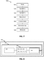
FIG. 7 shows a flow chart of a method in accordance with embodiments of the present invention. -
FIG. 8 shows a schematic diagram of a pixel array in accordance with embodiments of the present invention. - Any reference signs in the claims shall not be construed as limiting the scope.
- In the different drawings, the same reference signs refer to the same or analogous elements.
- The present invention will be described with respect to particular embodiments and with reference to certain drawings but the invention is not limited thereto but only by the claims. The drawings described are only schematic and are non-limiting. In the drawings, the size of some of the elements may be exaggerated and not drawn on scale for illustrative purposes. The dimensions and the relative dimensions do not correspond to actual reductions to practice of the invention.
- The terms first, second and the like in the description and in the claims, are used for distinguishing between similar elements and not necessarily for describing a sequence, either temporally, spatially, in ranking or in any other manner. It is to be understood that the terms so used are interchangeable under appropriate circumstances and that the embodiments of the invention described herein are capable of operation in other sequences than described or illustrated herein.
- It is to be noticed that the term "comprising", used in the claims, should not be interpreted as being restricted to the means listed thereafter; it does not exclude other elements or steps. It is thus to be interpreted as specifying the presence of the stated features, integers, steps or components as referred to, but does not preclude the presence or addition of one or more other features, integers, steps or components, or groups thereof. Thus, the scope of the expression "a device comprising means A and B" should not be limited to devices consisting only of components A and B. It means that with respect to the present invention, the only relevant components of the device are A and B.
- Reference throughout this specification to "one embodiment" or "an embodiment" means that a particular feature, structure or characteristic described in connection with the embodiment is included in at least one embodiment of the present invention. Thus, appearances of the phrases "in one embodiment" or "in an embodiment" in various places throughout this specification are not necessarily all referring to the same embodiment, but may. Furthermore, the particular features, structures or characteristics may be combined in any suitable manner, as would be apparent to one of ordinary skill in the art from this disclosure, in one or more embodiments.
- Similarly it should be appreciated that in the description of exemplary embodiments of the invention, various features of the invention are sometimes grouped together in a single embodiment, figure, or description thereof for the purpose of streamlining the disclosure and aiding in the understanding of one or more of the various inventive aspects. This method of disclosure, however, is not to be interpreted as reflecting an intention that the claimed invention requires more features than are expressly recited in each claim. Rather, as the following claims reflect, inventive aspects lie in less than all features of a single foregoing disclosed embodiment. Thus, the claims following the detailed description are hereby expressly incorporated into this detailed description, with each claim standing on its own as a separate embodiment of this invention.
- Furthermore, while some embodiments described herein include some but not other features included in other embodiments, combinations of features of different embodiments are meant to be within the scope of the invention, and form different embodiments, as would be understood by those in the art. For example, in the following claims, any of the claimed embodiments can be used in any combination.
- In the description provided herein, numerous specific details are set forth. However, it is understood that embodiments of the invention may be practiced without these specific details. In other instances, well-known methods, structures and techniques have not been shown in detail in order not to obscure an understanding of this description.
- In a first aspect embodiments of the present invention relate to a
sampling circuit 100 for correlated double sampling. - The
sampling circuit 100 comprises aninput node 110A, areset switch 120 which is electrically connected with its first node 120A to theinput node 110A, and which is electrically connected with its second node 120B to a first node 130A of afirst capacitor 130. Where in embodiments of the present invention reference is made to "electrically connected" reference is made to a connection by means of a conductive path. In embodiments of the present invention an electrical connection may be achieved through a closed switch. - The
sampling circuit 100, moreover, comprises asampling switch 140 electrically connected with its first node 140A to theinput node 110A, and electrically connected with its second node 140B to a first node 150A of asecond capacitor 150. - The
sampling circuit 100, moreover, comprises afirst reference node 110B and asecond reference node 110C. A second node 130B of thefirst capacitor 130 is adapted to be electrically connected with, or is electrically connected with, thefirst reference node 110B, and a second node 150B of thesecond capacitor 150 is adapted to be electrically connected with, or is electrically connected with, thesecond reference node 110C. Moreover, at least one of the second nodes 130B, 150B of the first orsecond capacitor reference switch 160. In embodiments of the present invention at least one of the second nodes 130B, 150B of the first orsecond capacitor - The
sampling circuit 100, moreover, comprises afirst switch 171 electrically connected with its first node 171A to the second node 130B of thefirst capacitor 130 and with its second node 171B to the first node 150A of thesecond capacitor 150. - The
sampling circuit 100, moreover, comprises asecond switch 172 electrically connected with its first node 172A to the first node 130A of thefirst capacitor 130 and with its second node 172B to the second node 150B of thesecond capacitor 150. - Sampling circuits in accordance with embodiments of the present invention are applicable to sample the voltage of integrating sensing elements. They are for example applicable for sensors/sensing devices which require CDS for the sampling kTC noise. Sampling circuits in accordance with embodiments of the present invention, moreover, may bring features such as level shifting and amplification. Sampling circuits in accordance with embodiments of the present invention may for example be conceived in the context of image sensors. The invention is, however, not limited thereto. Sampling circuits according to embodiments of the present invention may also be used for sampling other sensing elements where voltage sampling is required. The combination of a sampling circuit and a sensing element is a second aspect of the present invention and is further below referred to as a pixel.
- A
pixel 300 in accordance with embodiments of the present invention comprises asampling circuit 100 according to embodiments of the present invention and comprises asensor 200. Thesensor 200 comprises an integratingsensing element 210 of which asensor output pin 210A is directly or indirectly connected with theinput node 110A and comprises areset element 220 for resetting the integratingsensing element 210. - As discussed above the integrating sensing element may be any integrating sensor where voltage sampling is required. The integrating sensor may for example be an optical sensor.
-
Sampling circuits 100 in accordance with embodiments of the present invention are schematically illustrated inFIG. 1 to FIG. 4 . The principle of operating asampling circuit 100 in accordance with embodiments of the present invention is based on charge conservation and will be explained with the schematics ofFIG. 1 to FIG. 4 . - As a typical voltage sampling example, a typical 3 transistor structure such as used in imagers is shown. The
sensor 200, in accordance with embodiments of the present invention, comprises an integrating sensing element 210 (e.g. a photodiode), asampling switch 220 and abuffer 230. Thesensing element 210 may be extended to a 4T structure (pinned-photodiode) with an additional transfer gate. To measure the exact voltage, a sampling operation is required, which can generate large kTC noise at thesensor output pin 210A. Introducing thebuffer 230 will result in a higher sensitivity. -
FIG. 1 also shows asampling circuit 100 in accordance with embodiments of the present invention. Thesampling circuit 100 is adapted for correlated double sampling of a voltage from an integrating sensing element. In the exemplary embodiment illustrated inFIG. 1 the sampling circuit is present after thebuffer 230. Thesampling circuit 100 comprises twosampling capacitors switches first reference node 110B and the second node 130B of the first capacitor, and one between thesecond reference node 110C and the second node 150B of thesecond capacitor 150. Thefirst capacitor 130 and thesecond capacitor 150 may for example be implemented as passive capacitors, such as for example Metal-Insulator-Metal (MIM) capacitors. The invention is, however, not limited thereto and many other materials may be used. In some embodiments of the present invention thefirst capacitor 130 and thesecond capacitor 150 may be implemented as Metal-Oxide-Semiconductor Field-Effect Transistor (MOSFET) capacitors or as standalone capacitors. - A way of operating a
sampling circuit 100, in accordance with embodiments of the present invention, is explained in the paragraphs below. First the sensing element is reset by closing thereset switch 220. At a time t1, thereset switch 120 is switched OFF (i.e. it is opened), and a first voltage is sampled on the first capacitor 130 (of which the second node 130B is connected with a first reference voltage VREF1 which, in this example, is equal to VGND). This may for example be a reset voltage VRST. The reset voltage may for example be the sum of VRST,DC + VRST,n , wherein the VRST,DC corresponds with the reset DC voltage and VRST,n corresponds with the reset noise. This may for example comprise or mainly consist of the kTC noise. - At a time t2, the
sampling switch 140 is switched OFF for sampling a second voltage on the second capacitor 150 (of which the second node 150B is connected with a second reference voltage VREF2 which, in this example, is equal to VGND). The second voltage is obtained after integrating an incoming signal on thesensing element 210. The second voltage is also referred to as the sensing voltage VSIG. This may be the sum of VRST,DC + VRST,n + V Δ. In this example V Δ is the wanted sensing signal. - Hence, in the example of
FIG. 1 , the first capacitor has a charge of VRST . C 1(wherein C1 is the capacitance of the first capacitor 130) and the capacitor has a charge of VSIG ·C 2 (wherein C2 is the capacitance of the second capacitor 150). - At a time t3, the
reference switch 160 is turned OFF, leaving the second node of the first capacitor floating and hence, leaving the charge on thefirst capacitor 130 floating. Later, the subtraction is done by turning thefirst switch 171 and thesecond switch 172 ON (i.e. by closing them). By charge conservation, due to the flipped polarity of thefirst capacitor 130, a new combined voltage V 2 can be defined as:
second capacitor 150. This is the voltage on the floating node. - In embodiments of the present invention the
sampling circuit 100 may comprise acontroller 180 adapted for controlling some or all of the following switches: thereset switch 120, thesampling switch 140, thereference switch 160, thefirst switch 171, thesecond switch 172, and/or thereset element 120. The controller may be part of thesampling circuit 100. Alternatively the controller may be external. Controlling of the switches may be done according to the switching scheme explained in the previous paragraphs or according to a switching scheme explained in one of the following paragraphs. - Compared to the conventional CDS scheme, only three switches are added as overhead. Thus, a
sampling circuit 100 in accordance with embodiments of the present invention may be superior in power consumption, and/or in area and/or in noise. - In the exemplary embodiment illustrated in
FIG. 1 , areference switch 160 is connecting the second node 130B of thefirst capacitor 120 with thefirst reference node 110B. In another configuration areference switch 160 may be connecting the second node 150B of thesecond capacitor 150 with thesecond reference node 110C. An example thereof is illustrated inFIG. 2 . In yet another example reference switches may be present for both capacitors. - In the example of
FIG. 2 a similar switching scheme as forFIG. 1 may be applied. At the time t3, theswitch reference switch 160 is switched OFF, leaving the second node 150B of thesecond capacitor 150 floating and hence, leaving the charge on thesecond capacitor 150 floating. Later, the subtraction is done by turning thefirst switch 171 and thesecond switch 172 ON. Instead of subtracting the charge on thefirst capacitor 130, here the charge on thesecond capacitor 150 is subtracted. In this case, the voltage V1 on the first node 130A of thefirst capacitor 130 is the output to be read out and used (this corresponds with the voltage of the floating node). Thus, correlated double sampling with inversion is achieved. In this configuration, the inversion can be achieved as
- In embodiments of the present invention level shifting may be implemented by controlling the voltages of the first reference node and the second reference node. An example thereof is illustrated in
FIG. 3 . In this example the reset voltage VRST and the signal voltage VSIG are sampled against a reference voltage V REF1 on thefirst reference node 110B and a reference voltage V REF2 on thesecond reference node 110C, which leads to:
- In another exemplary embodiment of the present invention, as shown in
FIG. 4 , the voltage of V 1 can be obtained as:
- It is an advantage of embodiments of the present invention that the first reference voltage V REF1 and the second reference voltage V REF2, can be selected to optimize the implementation of the
first capacitor 130 and thesecond capacitor 150. For example, if a MOSFET transistor is used as capacitor, its capacitance can be varied against the gate-source voltage. By choosing a proper first reference voltage V REF1 and a second reference voltage V REF2, a more stable capacitance can be achieved with a certain signal swing. - Since the accuracy of the charge domain calculation will be affected by a mismatch between the capacitance values of the first capacitor and the second capacitor, it is advantageous that in some embodiments of the present invention the capacitances of the first and/or second capacitor are tuneable. In embodiments of the present invention the first and/or
second capacitor - In another exemplary embodiment of the present invention the capacitors may be implemented as a MOSFET or another voltage-controlled capacitor. In that case the capacitance values may be tuned by controlling the first reference voltage V REF1 and the second reference voltage V REF2 . The MOSFET can be biased to have a stable capacitance by e.g. tuning the threshold voltage Vt, the first reference voltage V REF1 and the second reference voltage V REF2, or by introducing depletion mode transistors.
- In embodiments of the present invention the
sampling circuit 100 may be adapted for decreasing the capacitance values of thecapacitors - In embodiments of the present invention MOSFETs may for example be used to implement the first and second capacitor. In that case it may for example be that the MOSFET cannot be biased well enough to ensure a stable capacitance. In these embodiments it may be advantageous that an additional amplification can be introduced for better noise performance.
- A MOSFET typically has a high sheet capacitance, which is typically not very linear (see
FIG. 5 ). However, in embodiments of the present invention, it is possible to take advantage of this non-linearity of the capacitance versus voltage to realize a gain. Due to the CDS, by setting the right voltages, the first and/or the second transistor can be forced moving from the inversion into depletion region. This leads to a lower capacitance (CS, DEP instead of CS, INV), thus creating a voltage gain, since the charge on the sampling capacitor after the CDS is reserved constant. One must, however, take into account that linearity may degrade in this case. - The kTC noise from the sampling of VRST and VSIG (which is an inherit problem for all CDS techniques), may be reduced by increasing the capacitance value of the first and second capacitor. Sampling circuits according to embodiments of the present invention may result in a decreased signal gain. The effective gain of the CDS operation of a sampling circuit in accordance with embodiments of the present invention is 0.5. This may have a noise impact on the following blocks. This can for example be recovered by MOSFET amplification at the cost of linearity.
- A
sampling circuit 100 according to an exemplary embodiment of the present invention may additionally comprise amemory bank 190 or avoltage buffer 190 following V1 or V2 for voltage sensing. An example thereof is schematically shown inFIG. 6 . Thesampling circuit 100 inFIG. 6 may for example be a sampling circuit with CDS and inversion, and optional amplification, in accordance with embodiments of the present invention. It is adapted for sampling the sensor output voltage of asensor 200. - In a third aspect, embodiments of the present invention relate to a
pixel array 400 comprising a plurality ofpixels 300 in accordance with embodiments of the present invention. An example thereof is illustrated inFIG. 8 . It shows apixel array 400 comprising a plurality ofpixels 300 in accordance with embodiments of the present invention. Also in this example thesampling circuit 100 may additionally comprise amemory bank 190 or avoltage buffer 190. -
Sampling circuits 100 according to embodiments of the present invention may be used in image sensors to implement column level CDS or even pixel CDS. It is, moreover, advantageous that along with the CDS, level shifting can be easily realized at the same time. - In a fourth aspect, embodiments of the present invention relate to a
method 500 for correlated double sampling a signal from an integrating sensing element. The method comprises: - resetting 510 the sensing element,
- sampling a
first voltage 520 on afirst capacitor 130, wherein the first voltage is obtained from an output of the sensing element connected with a first node 130A of the first capacitor, and wherein a second node 130B of the first capacitor is connected with afirst reference voltage 110B, - sampling a
second voltage 530 on asecond capacitor 150, wherein the second voltage is obtained from the output of the sensing element, after integrating an incoming signal on the sensing element, and wherein a second node 150B of thesecond capacitor 150 is connected with asecond reference voltage 110C, - disconnecting 540 the second node of the first or the second capacitor from the first respectively second reference voltage thus obtaining a floating node, and cross-connecting 550 the
first capacitor 130 and thesecond capacitor 150 wherein nodes with opposite polarities are connected, - measuring 560 a voltage on the floating node.
- Sampling circuits according to embodiments of the present invention may comprise a controller adapted for controlling the switches in accordance with the method described above.
- A flow chart of an exemplary method in accordance with embodiments of the present invention is shown in
FIG. 7 . The first reference voltage and the second reference voltage may be tunable. They may be different from zero. Thus level shifting may be applied. In embodiments of the present invention the first reference voltage and the second reference voltage may be electrical ground. A method in accordance with embodiments of the present invention optionally may comprise decreasing 555 the capacitance values of the capacitors after sampling the first and the second voltage and before measuring the voltage on the floating node. - In summary, because of the CDS with only a limited number of switches it is an advantage of embodiments of the present invention that a low noise, low power, low area, and easily controllable sampling circuit is obtained. This is particularly the case because the subtraction is done with a few switches and capacitors without using amplifiers.
- Moreover, in particular embodiments of the present invention, flexible, precise level shifting is enabled. By adjusting the reference voltages, the sensor output can be level shifted to almost any arbitrary voltage.
Claims (15)
- A sampling circuit (100) for correlated double sampling, the sampling circuit comprising:- an input node (110A),- a reset switch (120) electrically connected with its first node (120A) to the input node (110A), and electrically connected with its second node (120B) to a first node (130A) of a first capacitor (130),- a sampling switch (140) electrically connected with its first node (140A) to the input node (110A), and electrically connected with its second node (140B) to a first node (150A) of a second capacitor (150),- a first reference node (110B), a second reference node (110C), wherein a second node (130B) of the first capacitor (130) is adapted to be electrically connected with, or is electrically connected with, the first reference node (110B), and a second node (150B) of the second capacitor (150) is adapted to be electrically connected with, or is electrically connected with, the second reference node (110C), and wherein at least one of the second nodes (130B, 150B) of the first or second capacitor (130, 150) can be electrically connected with the corresponding reference node using a reference switch (160),- a first switch (171) electrically connected with its first node (171A) to the second node (130B) of the first capacitor (130) and with its second node (171B) to the first node (150A) of the second capacitor (150),- a second switch (172) electrically connected with its first node (172A) to the first node (130A) of the first capacitor (130) and with its second node (172B) to the second node (150B) of the second capacitor (150).
- A sampling circuit (100) according to claim 1 wherein the first capacitor (130) and the second capacitor (150) have the same capacitance value.
- A sampling circuit (100) according to any of the previous claims wherein the first capacitor (130) is tunable and/or wherein the second capacitor (150) is tunable.
- A sampling circuit (100) according to any of the previous claims wherein the first capacitor (130) is a voltage controlled capacitor and/or wherein the second capacitor (150) is a voltage controlled capacitor.
- A sampling circuit (100) according to any of the previous claims wherein the first capacitor (130) and/or wherein the second capacitor (150) is a MOSFET.
- A sampling circuit (100) according to any of the previous claims, the sampling circuit (100) comprising a controller (180) adapted for- sampling a first voltage from the input node (110A) on the first capacitor (130) by opening the reset switch (120),- and for sampling a second voltage from the input node (110A) on the second capacitor (150) by opening the sampling switch (140),- and for opening the reference switch (160) after sampling the first and the second voltage, and for closing the first switch (171) and the second switch (172) after opening the reference switch (160).
- A sampling circuit (100) according to claim 6, wherein the sampling circuit is adapted for decreasing the capacitance values of the first and second capacitor (130, 150) after opening the reference switch (160).
- A pixel (300) comprising a sampling circuit (100) according to any of the claims 1 to 7 and comprising a sensor (200) which comprises an integrating sensing element (210) of which a sensor output pin (210A) is directly or indirectly connected with the input node (110A) and which comprises a reset element (220) for resetting the integrating sensing element (210).
- A pixel (300) according to claim 8 with the sampling circuit (100) according to claim 6, wherein the controller (180) is adapted for:- resetting the sensing element (210) using the reset element (220), and for sampling the first voltage after resetting the sensing element (210),- and for sampling the second voltage after integration of an incoming signal on the sensing element (210).
- A pixel (300) according to claim 8 or 9 wherein the integrating sensing element (210) is a photodiode or a pinned photodiode.
- A pixel array (400) comprising a plurality of pixels (200) according to any of the claims 8 to 10 wherein the pixels are arranged in an array.
- A pixel array (400) with the plurality of pixels (200) according to claim 9 wherein the controller (180) is shared between the pixels.
- A method (500) for correlated double sampling a signal from an integrating sensing element, the method comprising:- resetting (510) the sensing element,- sampling a first voltage (520) on a first capacitor, wherein the first voltage is obtained from an output of the sensing element connected with a first node of the first capacitor, and wherein a second node of the first capacitor is connected with a first reference voltage,- sampling a second voltage (530) on a second capacitor, wherein the second voltage is obtained from the output of the sensing element, after integrating an incoming signal on the sensing element, and wherein a second node of the second capacitor is connected with a second reference voltage,- disconnecting (540) the second node of the first or the second capacitor from the first respectively second reference voltage thus obtaining a floating node, and cross-connecting (550) the first capacitor and the second capacitor wherein nodes with opposite polarities are connected,- measuring (560) a voltage on the floating node.
- A method (500) according to claim 13 wherein the first reference voltage and the second reference voltage are the same or wherein the first reference voltage and the second reference voltage are electrical ground.
- A method (500) according to any of the claims 13 or 14, the method comprising decreasing (155) the capacitance values of the capacitors after sampling the first and the second voltage and before measuring the voltage on the floating node.
Priority Applications (2)
| Application Number | Priority Date | Filing Date | Title |
|---|---|---|---|
| EP19183766.5A EP3761632B1 (en) | 2019-07-02 | 2019-07-02 | Correlated double sampling circuit and method |
| US16/918,970 US11165981B2 (en) | 2019-07-02 | 2020-07-01 | System and method for correlated double sampling |
Applications Claiming Priority (1)
| Application Number | Priority Date | Filing Date | Title |
|---|---|---|---|
| EP19183766.5A EP3761632B1 (en) | 2019-07-02 | 2019-07-02 | Correlated double sampling circuit and method |
Publications (2)
| Publication Number | Publication Date |
|---|---|
| EP3761632A1 true EP3761632A1 (en) | 2021-01-06 |
| EP3761632B1 EP3761632B1 (en) | 2022-03-02 |
Family
ID=67145546
Family Applications (1)
| Application Number | Title | Priority Date | Filing Date |
|---|---|---|---|
| EP19183766.5A Active EP3761632B1 (en) | 2019-07-02 | 2019-07-02 | Correlated double sampling circuit and method |
Country Status (2)
| Country | Link |
|---|---|
| US (1) | US11165981B2 (en) |
| EP (1) | EP3761632B1 (en) |
Families Citing this family (1)
| Publication number | Priority date | Publication date | Assignee | Title |
|---|---|---|---|---|
| US12328519B2 (en) * | 2022-02-15 | 2025-06-10 | Novatek Microelectronics Corp. | Image sensor |
Citations (3)
| Publication number | Priority date | Publication date | Assignee | Title |
|---|---|---|---|---|
| US7277129B1 (en) * | 2002-10-31 | 2007-10-02 | Sensata Technologies, Inc. | Pixel design including in-pixel correlated double sampling circuit |
| US7612817B2 (en) | 2001-11-06 | 2009-11-03 | Hiok Nam Tay | CMOS image sensor with noise cancellation |
| US20170374307A1 (en) * | 2016-06-24 | 2017-12-28 | Qualcomm Incorporated | Low-power and low-mismatch correlated double sampling (cds) circuit |
Family Cites Families (5)
| Publication number | Priority date | Publication date | Assignee | Title |
|---|---|---|---|---|
| US7321111B2 (en) | 2004-04-12 | 2008-01-22 | Canesta, Inc. | Method and system to enhance differential dynamic range and signal/noise in CMOS range finding systems using differential sensors |
| US7167119B1 (en) * | 2005-12-20 | 2007-01-23 | Cirrus Logic, Inc. | Delta-sigma modulators with double sampling input networks and systems using the same |
| JP5395323B2 (en) | 2006-09-29 | 2014-01-22 | ブレインビジョン株式会社 | Solid-state image sensor |
| EP2116864A1 (en) | 2008-05-09 | 2009-11-11 | Vrije Universiteit Brussel | TOF range finding with background radiation suppression |
| US9019480B2 (en) | 2013-02-26 | 2015-04-28 | Jds Uniphase Corporation | Time-of-flight (TOF) system, sensor pixel, and method |
-
2019
- 2019-07-02 EP EP19183766.5A patent/EP3761632B1/en active Active
-
2020
- 2020-07-01 US US16/918,970 patent/US11165981B2/en active Active
Patent Citations (3)
| Publication number | Priority date | Publication date | Assignee | Title |
|---|---|---|---|---|
| US7612817B2 (en) | 2001-11-06 | 2009-11-03 | Hiok Nam Tay | CMOS image sensor with noise cancellation |
| US7277129B1 (en) * | 2002-10-31 | 2007-10-02 | Sensata Technologies, Inc. | Pixel design including in-pixel correlated double sampling circuit |
| US20170374307A1 (en) * | 2016-06-24 | 2017-12-28 | Qualcomm Incorporated | Low-power and low-mismatch correlated double sampling (cds) circuit |
Also Published As
| Publication number | Publication date |
|---|---|
| US20210006739A1 (en) | 2021-01-07 |
| US11165981B2 (en) | 2021-11-02 |
| EP3761632B1 (en) | 2022-03-02 |
Similar Documents
| Publication | Publication Date | Title |
|---|---|---|
| CN102547170B (en) | Imaging device | |
| KR940002810B1 (en) | Sample / Hold Circuit Device | |
| US9530356B2 (en) | Source driver of display device | |
| US7791380B2 (en) | Current sampling method and circuit | |
| JP2022507996A (en) | Touch detection circuit, touch display device and touch detection method | |
| US20200200603A1 (en) | Optical sensor arrangement and method for light sensing | |
| US9270905B2 (en) | Readout circuit, solid-state imaging apparatus, and method for driving readout circuit | |
| EP0598308B1 (en) | Differential comparator circuit | |
| US9426388B2 (en) | Semiconductor device and infrared image pickup device provided with same | |
| US10298216B2 (en) | Semiconductor device | |
| EP1333661A1 (en) | Improved image sensor | |
| US20210320143A1 (en) | Image sensor and imaging system comprising the same | |
| JP7453868B2 (en) | Image sensor and imaging system including the image sensor | |
| Poujois et al. | Low-level MOS transistor amplifier using storage techniques | |
| EP1942663A1 (en) | Column current source | |
| EP3761632B1 (en) | Correlated double sampling circuit and method | |
| JP5765274B2 (en) | Analog switch | |
| US7414464B2 (en) | Op driver with the function of canceling op offset | |
| JP3801112B2 (en) | Image reading signal processing apparatus | |
| US6693479B1 (en) | Boost structures for switched-capacitor systems | |
| US7372319B1 (en) | Constant boosted voltage generator circuit for feedback switches in a switched capacitor circuit | |
| JP4744325B2 (en) | Signal amplifier | |
| JP2007187509A (en) | Capacitive physical quantity sensor | |
| US7786794B2 (en) | Amplifier circuit | |
| JP3644445B2 (en) | Image reading signal processing apparatus |
Legal Events
| Date | Code | Title | Description |
|---|---|---|---|
| PUAI | Public reference made under article 153(3) epc to a published international application that has entered the european phase |
Free format text: ORIGINAL CODE: 0009012 |
|
| STAA | Information on the status of an ep patent application or granted ep patent |
Free format text: STATUS: THE APPLICATION HAS BEEN PUBLISHED |
|
| AK | Designated contracting states |
Kind code of ref document: A1 Designated state(s): AL AT BE BG CH CY CZ DE DK EE ES FI FR GB GR HR HU IE IS IT LI LT LU LV MC MK MT NL NO PL PT RO RS SE SI SK SM TR |
|
| AX | Request for extension of the european patent |
Extension state: BA ME |
|
| STAA | Information on the status of an ep patent application or granted ep patent |
Free format text: STATUS: REQUEST FOR EXAMINATION WAS MADE |
|
| 17P | Request for examination filed |
Effective date: 20210608 |
|
| RBV | Designated contracting states (corrected) |
Designated state(s): AL AT BE BG CH CY CZ DE DK EE ES FI FR GB GR HR HU IE IS IT LI LT LU LV MC MK MT NL NO PL PT RO RS SE SI SK SM TR |
|
| GRAP | Despatch of communication of intention to grant a patent |
Free format text: ORIGINAL CODE: EPIDOSNIGR1 |
|
| STAA | Information on the status of an ep patent application or granted ep patent |
Free format text: STATUS: GRANT OF PATENT IS INTENDED |
|
| INTG | Intention to grant announced |
Effective date: 20211129 |
|
| GRAS | Grant fee paid |
Free format text: ORIGINAL CODE: EPIDOSNIGR3 |
|
| GRAA | (expected) grant |
Free format text: ORIGINAL CODE: 0009210 |
|
| STAA | Information on the status of an ep patent application or granted ep patent |
Free format text: STATUS: THE PATENT HAS BEEN GRANTED |
|
| AK | Designated contracting states |
Kind code of ref document: B1 Designated state(s): AL AT BE BG CH CY CZ DE DK EE ES FI FR GB GR HR HU IE IS IT LI LT LU LV MC MK MT NL NO PL PT RO RS SE SI SK SM TR |
|
| REG | Reference to a national code |
Ref country code: GB Ref legal event code: FG4D |
|
| REG | Reference to a national code |
Ref country code: CH Ref legal event code: EP Ref country code: AT Ref legal event code: REF Ref document number: 1473228 Country of ref document: AT Kind code of ref document: T Effective date: 20220315 |
|
| REG | Reference to a national code |
Ref country code: DE Ref legal event code: R096 Ref document number: 602019012027 Country of ref document: DE |
|
| REG | Reference to a national code |
Ref country code: IE Ref legal event code: FG4D |
|
| REG | Reference to a national code |
Ref country code: LT Ref legal event code: MG9D |
|
| REG | Reference to a national code |
Ref country code: NL Ref legal event code: MP Effective date: 20220302 |
|
| PG25 | Lapsed in a contracting state [announced via postgrant information from national office to epo] |
Ref country code: SE Free format text: LAPSE BECAUSE OF FAILURE TO SUBMIT A TRANSLATION OF THE DESCRIPTION OR TO PAY THE FEE WITHIN THE PRESCRIBED TIME-LIMIT Effective date: 20220302 Ref country code: RS Free format text: LAPSE BECAUSE OF FAILURE TO SUBMIT A TRANSLATION OF THE DESCRIPTION OR TO PAY THE FEE WITHIN THE PRESCRIBED TIME-LIMIT Effective date: 20220302 Ref country code: NO Free format text: LAPSE BECAUSE OF FAILURE TO SUBMIT A TRANSLATION OF THE DESCRIPTION OR TO PAY THE FEE WITHIN THE PRESCRIBED TIME-LIMIT Effective date: 20220602 Ref country code: LT Free format text: LAPSE BECAUSE OF FAILURE TO SUBMIT A TRANSLATION OF THE DESCRIPTION OR TO PAY THE FEE WITHIN THE PRESCRIBED TIME-LIMIT Effective date: 20220302 Ref country code: HR Free format text: LAPSE BECAUSE OF FAILURE TO SUBMIT A TRANSLATION OF THE DESCRIPTION OR TO PAY THE FEE WITHIN THE PRESCRIBED TIME-LIMIT Effective date: 20220302 Ref country code: ES Free format text: LAPSE BECAUSE OF FAILURE TO SUBMIT A TRANSLATION OF THE DESCRIPTION OR TO PAY THE FEE WITHIN THE PRESCRIBED TIME-LIMIT Effective date: 20220302 Ref country code: BG Free format text: LAPSE BECAUSE OF FAILURE TO SUBMIT A TRANSLATION OF THE DESCRIPTION OR TO PAY THE FEE WITHIN THE PRESCRIBED TIME-LIMIT Effective date: 20220602 |
|
| REG | Reference to a national code |
Ref country code: AT Ref legal event code: MK05 Ref document number: 1473228 Country of ref document: AT Kind code of ref document: T Effective date: 20220302 |
|
| PG25 | Lapsed in a contracting state [announced via postgrant information from national office to epo] |
Ref country code: PL Free format text: LAPSE BECAUSE OF FAILURE TO SUBMIT A TRANSLATION OF THE DESCRIPTION OR TO PAY THE FEE WITHIN THE PRESCRIBED TIME-LIMIT Effective date: 20220302 Ref country code: LV Free format text: LAPSE BECAUSE OF FAILURE TO SUBMIT A TRANSLATION OF THE DESCRIPTION OR TO PAY THE FEE WITHIN THE PRESCRIBED TIME-LIMIT Effective date: 20220302 Ref country code: GR Free format text: LAPSE BECAUSE OF FAILURE TO SUBMIT A TRANSLATION OF THE DESCRIPTION OR TO PAY THE FEE WITHIN THE PRESCRIBED TIME-LIMIT Effective date: 20220603 Ref country code: FI Free format text: LAPSE BECAUSE OF FAILURE TO SUBMIT A TRANSLATION OF THE DESCRIPTION OR TO PAY THE FEE WITHIN THE PRESCRIBED TIME-LIMIT Effective date: 20220302 |
|
| PG25 | Lapsed in a contracting state [announced via postgrant information from national office to epo] |
Ref country code: NL Free format text: LAPSE BECAUSE OF FAILURE TO SUBMIT A TRANSLATION OF THE DESCRIPTION OR TO PAY THE FEE WITHIN THE PRESCRIBED TIME-LIMIT Effective date: 20220302 |
|
| PG25 | Lapsed in a contracting state [announced via postgrant information from national office to epo] |
Ref country code: SM Free format text: LAPSE BECAUSE OF FAILURE TO SUBMIT A TRANSLATION OF THE DESCRIPTION OR TO PAY THE FEE WITHIN THE PRESCRIBED TIME-LIMIT Effective date: 20220302 Ref country code: SK Free format text: LAPSE BECAUSE OF FAILURE TO SUBMIT A TRANSLATION OF THE DESCRIPTION OR TO PAY THE FEE WITHIN THE PRESCRIBED TIME-LIMIT Effective date: 20220302 Ref country code: RO Free format text: LAPSE BECAUSE OF FAILURE TO SUBMIT A TRANSLATION OF THE DESCRIPTION OR TO PAY THE FEE WITHIN THE PRESCRIBED TIME-LIMIT Effective date: 20220302 Ref country code: PT Free format text: LAPSE BECAUSE OF FAILURE TO SUBMIT A TRANSLATION OF THE DESCRIPTION OR TO PAY THE FEE WITHIN THE PRESCRIBED TIME-LIMIT Effective date: 20220704 Ref country code: EE Free format text: LAPSE BECAUSE OF FAILURE TO SUBMIT A TRANSLATION OF THE DESCRIPTION OR TO PAY THE FEE WITHIN THE PRESCRIBED TIME-LIMIT Effective date: 20220302 Ref country code: CZ Free format text: LAPSE BECAUSE OF FAILURE TO SUBMIT A TRANSLATION OF THE DESCRIPTION OR TO PAY THE FEE WITHIN THE PRESCRIBED TIME-LIMIT Effective date: 20220302 Ref country code: AT Free format text: LAPSE BECAUSE OF FAILURE TO SUBMIT A TRANSLATION OF THE DESCRIPTION OR TO PAY THE FEE WITHIN THE PRESCRIBED TIME-LIMIT Effective date: 20220302 |
|
| REG | Reference to a national code |
Ref country code: DE Ref legal event code: R079 Ref document number: 602019012027 Country of ref document: DE Free format text: PREVIOUS MAIN CLASS: H04N0005378000 Ipc: H04N0025780000 |
|
| PG25 | Lapsed in a contracting state [announced via postgrant information from national office to epo] |
Ref country code: IS Free format text: LAPSE BECAUSE OF FAILURE TO SUBMIT A TRANSLATION OF THE DESCRIPTION OR TO PAY THE FEE WITHIN THE PRESCRIBED TIME-LIMIT Effective date: 20220702 Ref country code: AL Free format text: LAPSE BECAUSE OF FAILURE TO SUBMIT A TRANSLATION OF THE DESCRIPTION OR TO PAY THE FEE WITHIN THE PRESCRIBED TIME-LIMIT Effective date: 20220302 |
|
| REG | Reference to a national code |
Ref country code: DE Ref legal event code: R097 Ref document number: 602019012027 Country of ref document: DE |
|
| PLBE | No opposition filed within time limit |
Free format text: ORIGINAL CODE: 0009261 |
|
| STAA | Information on the status of an ep patent application or granted ep patent |
Free format text: STATUS: NO OPPOSITION FILED WITHIN TIME LIMIT |
|
| PG25 | Lapsed in a contracting state [announced via postgrant information from national office to epo] |
Ref country code: DK Free format text: LAPSE BECAUSE OF FAILURE TO SUBMIT A TRANSLATION OF THE DESCRIPTION OR TO PAY THE FEE WITHIN THE PRESCRIBED TIME-LIMIT Effective date: 20220302 |
|
| 26N | No opposition filed |
Effective date: 20221205 |
|
| PG25 | Lapsed in a contracting state [announced via postgrant information from national office to epo] |
Ref country code: SI Free format text: LAPSE BECAUSE OF FAILURE TO SUBMIT A TRANSLATION OF THE DESCRIPTION OR TO PAY THE FEE WITHIN THE PRESCRIBED TIME-LIMIT Effective date: 20220302 Ref country code: MC Free format text: LAPSE BECAUSE OF FAILURE TO SUBMIT A TRANSLATION OF THE DESCRIPTION OR TO PAY THE FEE WITHIN THE PRESCRIBED TIME-LIMIT Effective date: 20220302 |
|
| REG | Reference to a national code |
Ref country code: CH Ref legal event code: PL |
|
| REG | Reference to a national code |
Ref country code: BE Ref legal event code: MM Effective date: 20220731 |
|
| PG25 | Lapsed in a contracting state [announced via postgrant information from national office to epo] |
Ref country code: LU Free format text: LAPSE BECAUSE OF NON-PAYMENT OF DUE FEES Effective date: 20220702 Ref country code: LI Free format text: LAPSE BECAUSE OF NON-PAYMENT OF DUE FEES Effective date: 20220731 Ref country code: FR Free format text: LAPSE BECAUSE OF NON-PAYMENT OF DUE FEES Effective date: 20220731 Ref country code: CH Free format text: LAPSE BECAUSE OF NON-PAYMENT OF DUE FEES Effective date: 20220731 |
|
| PG25 | Lapsed in a contracting state [announced via postgrant information from national office to epo] |
Ref country code: BE Free format text: LAPSE BECAUSE OF NON-PAYMENT OF DUE FEES Effective date: 20220731 |
|
| P01 | Opt-out of the competence of the unified patent court (upc) registered |
Effective date: 20230513 |
|
| PG25 | Lapsed in a contracting state [announced via postgrant information from national office to epo] |
Ref country code: IT Free format text: LAPSE BECAUSE OF FAILURE TO SUBMIT A TRANSLATION OF THE DESCRIPTION OR TO PAY THE FEE WITHIN THE PRESCRIBED TIME-LIMIT Effective date: 20220302 Ref country code: IE Free format text: LAPSE BECAUSE OF NON-PAYMENT OF DUE FEES Effective date: 20220702 |
|
| GBPC | Gb: european patent ceased through non-payment of renewal fee |
Effective date: 20230702 |
|
| PG25 | Lapsed in a contracting state [announced via postgrant information from national office to epo] |
Ref country code: MK Free format text: LAPSE BECAUSE OF FAILURE TO SUBMIT A TRANSLATION OF THE DESCRIPTION OR TO PAY THE FEE WITHIN THE PRESCRIBED TIME-LIMIT Effective date: 20220302 Ref country code: CY Free format text: LAPSE BECAUSE OF FAILURE TO SUBMIT A TRANSLATION OF THE DESCRIPTION OR TO PAY THE FEE WITHIN THE PRESCRIBED TIME-LIMIT Effective date: 20220302 Ref country code: GB Free format text: LAPSE BECAUSE OF NON-PAYMENT OF DUE FEES Effective date: 20230702 |
|
| PG25 | Lapsed in a contracting state [announced via postgrant information from national office to epo] |
Ref country code: HU Free format text: LAPSE BECAUSE OF FAILURE TO SUBMIT A TRANSLATION OF THE DESCRIPTION OR TO PAY THE FEE WITHIN THE PRESCRIBED TIME-LIMIT; INVALID AB INITIO Effective date: 20190702 |
|
| PG25 | Lapsed in a contracting state [announced via postgrant information from national office to epo] |
Ref country code: TR Free format text: LAPSE BECAUSE OF FAILURE TO SUBMIT A TRANSLATION OF THE DESCRIPTION OR TO PAY THE FEE WITHIN THE PRESCRIBED TIME-LIMIT Effective date: 20220302 |
|
| PG25 | Lapsed in a contracting state [announced via postgrant information from national office to epo] |
Ref country code: MT Free format text: LAPSE BECAUSE OF FAILURE TO SUBMIT A TRANSLATION OF THE DESCRIPTION OR TO PAY THE FEE WITHIN THE PRESCRIBED TIME-LIMIT Effective date: 20220302 |
|
| PGFP | Annual fee paid to national office [announced via postgrant information from national office to epo] |
Ref country code: DE Payment date: 20250620 Year of fee payment: 7 |