EP3761630B1 - Imaging device, imaging system, and mobile object - Google Patents
Imaging device, imaging system, and mobile object Download PDFInfo
- Publication number
- EP3761630B1 EP3761630B1 EP19761044.7A EP19761044A EP3761630B1 EP 3761630 B1 EP3761630 B1 EP 3761630B1 EP 19761044 A EP19761044 A EP 19761044A EP 3761630 B1 EP3761630 B1 EP 3761630B1
- Authority
- EP
- European Patent Office
- Prior art keywords
- image capturing
- lifetime
- capturing apparatus
- image sensor
- unit
- Prior art date
- Legal status (The legal status is an assumption and is not a legal conclusion. Google has not performed a legal analysis and makes no representation as to the accuracy of the status listed.)
- Active
Links
Images







Classifications
-
- G—PHYSICS
- G01—MEASURING; TESTING
- G01R—MEASURING ELECTRIC VARIABLES; MEASURING MAGNETIC VARIABLES
- G01R31/00—Arrangements for testing electric properties; Arrangements for locating electric faults; Arrangements for electrical testing characterised by what is being tested not provided for elsewhere
- G01R31/26—Testing of individual semiconductor devices
- G01R31/2642—Testing semiconductor operation lifetime or reliability, e.g. by accelerated life tests
-
- B—PERFORMING OPERATIONS; TRANSPORTING
- B60—VEHICLES IN GENERAL
- B60K—ARRANGEMENT OR MOUNTING OF PROPULSION UNITS OR OF TRANSMISSIONS IN VEHICLES; ARRANGEMENT OR MOUNTING OF PLURAL DIVERSE PRIME-MOVERS IN VEHICLES; AUXILIARY DRIVES FOR VEHICLES; INSTRUMENTATION OR DASHBOARDS FOR VEHICLES; ARRANGEMENTS IN CONNECTION WITH COOLING, AIR INTAKE, GAS EXHAUST OR FUEL SUPPLY OF PROPULSION UNITS IN VEHICLES
- B60K35/00—Instruments specially adapted for vehicles; Arrangement of instruments in or on vehicles
- B60K35/20—Output arrangements, i.e. from vehicle to user, associated with vehicle functions or specially adapted therefor
- B60K35/29—Instruments characterised by the way in which information is handled, e.g. showing information on plural displays or prioritising information according to driving conditions
-
- G—PHYSICS
- G01—MEASURING; TESTING
- G01R—MEASURING ELECTRIC VARIABLES; MEASURING MAGNETIC VARIABLES
- G01R31/00—Arrangements for testing electric properties; Arrangements for locating electric faults; Arrangements for electrical testing characterised by what is being tested not provided for elsewhere
- G01R31/26—Testing of individual semiconductor devices
- G01R31/2607—Circuits therefor
- G01R31/2632—Circuits therefor for testing diodes
- G01R31/2635—Testing light-emitting diodes, laser diodes or photodiodes
-
- G—PHYSICS
- G01—MEASURING; TESTING
- G01R—MEASURING ELECTRIC VARIABLES; MEASURING MAGNETIC VARIABLES
- G01R31/00—Arrangements for testing electric properties; Arrangements for locating electric faults; Arrangements for electrical testing characterised by what is being tested not provided for elsewhere
- G01R31/26—Testing of individual semiconductor devices
- G01R31/27—Testing of devices without physical removal from the circuit of which they form part, e.g. compensating for effects surrounding elements
-
- H—ELECTRICITY
- H04—ELECTRIC COMMUNICATION TECHNIQUE
- H04N—PICTORIAL COMMUNICATION, e.g. TELEVISION
- H04N17/00—Diagnosis, testing or measuring for television systems or their details
- H04N17/002—Diagnosis, testing or measuring for television systems or their details for television cameras
-
- H—ELECTRICITY
- H04—ELECTRIC COMMUNICATION TECHNIQUE
- H04N—PICTORIAL COMMUNICATION, e.g. TELEVISION
- H04N25/00—Circuitry of solid-state image sensors [SSIS]; Control thereof
- H04N25/40—Extracting pixel data from image sensors by controlling scanning circuits, e.g. by modifying the number of pixels sampled or to be sampled
- H04N25/44—Extracting pixel data from image sensors by controlling scanning circuits, e.g. by modifying the number of pixels sampled or to be sampled by partially reading an SSIS array
-
- H—ELECTRICITY
- H04—ELECTRIC COMMUNICATION TECHNIQUE
- H04N—PICTORIAL COMMUNICATION, e.g. TELEVISION
- H04N25/00—Circuitry of solid-state image sensors [SSIS]; Control thereof
- H04N25/70—SSIS architectures; Circuits associated therewith
- H04N25/709—Circuitry for control of the power supply
-
- H—ELECTRICITY
- H04—ELECTRIC COMMUNICATION TECHNIQUE
- H04N—PICTORIAL COMMUNICATION, e.g. TELEVISION
- H04N25/00—Circuitry of solid-state image sensors [SSIS]; Control thereof
- H04N25/70—SSIS architectures; Circuits associated therewith
- H04N25/76—Addressed sensors, e.g. MOS or CMOS sensors
-
- H—ELECTRICITY
- H10—SEMICONDUCTOR DEVICES; ELECTRIC SOLID-STATE DEVICES NOT OTHERWISE PROVIDED FOR
- H10D—INORGANIC ELECTRIC SEMICONDUCTOR DEVICES
- H10D84/00—Integrated devices formed in or on semiconductor substrates that comprise only semiconducting layers, e.g. on Si wafers or on GaAs-on-Si wafers
-
- H—ELECTRICITY
- H10—SEMICONDUCTOR DEVICES; ELECTRIC SOLID-STATE DEVICES NOT OTHERWISE PROVIDED FOR
- H10D—INORGANIC ELECTRIC SEMICONDUCTOR DEVICES
- H10D84/00—Integrated devices formed in or on semiconductor substrates that comprise only semiconducting layers, e.g. on Si wafers or on GaAs-on-Si wafers
- H10D84/01—Manufacture or treatment
- H10D84/02—Manufacture or treatment characterised by using material-based technologies
- H10D84/03—Manufacture or treatment characterised by using material-based technologies using Group IV technology, e.g. silicon technology or silicon-carbide [SiC] technology
- H10D84/038—Manufacture or treatment characterised by using material-based technologies using Group IV technology, e.g. silicon technology or silicon-carbide [SiC] technology using silicon technology, e.g. SiGe
-
- H—ELECTRICITY
- H10—SEMICONDUCTOR DEVICES; ELECTRIC SOLID-STATE DEVICES NOT OTHERWISE PROVIDED FOR
- H10F—INORGANIC SEMICONDUCTOR DEVICES SENSITIVE TO INFRARED RADIATION, LIGHT, ELECTROMAGNETIC RADIATION OF SHORTER WAVELENGTH OR CORPUSCULAR RADIATION
- H10F39/00—Integrated devices, or assemblies of multiple devices, comprising at least one element covered by group H10F30/00, e.g. radiation detectors comprising photodiode arrays
- H10F39/10—Integrated devices
- H10F39/12—Image sensors
- H10F39/18—Complementary metal-oxide-semiconductor [CMOS] image sensors; Photodiode array image sensors
-
- B—PERFORMING OPERATIONS; TRANSPORTING
- B60—VEHICLES IN GENERAL
- B60K—ARRANGEMENT OR MOUNTING OF PROPULSION UNITS OR OF TRANSMISSIONS IN VEHICLES; ARRANGEMENT OR MOUNTING OF PLURAL DIVERSE PRIME-MOVERS IN VEHICLES; AUXILIARY DRIVES FOR VEHICLES; INSTRUMENTATION OR DASHBOARDS FOR VEHICLES; ARRANGEMENTS IN CONNECTION WITH COOLING, AIR INTAKE, GAS EXHAUST OR FUEL SUPPLY OF PROPULSION UNITS IN VEHICLES
- B60K2360/00—Indexing scheme associated with groups B60K35/00 or B60K37/00 relating to details of instruments or dashboards
- B60K2360/40—Hardware adaptations for dashboards or instruments
- B60K2360/48—Sensors
Definitions
- the present invention relates to an image capturing apparatus, an image capturing system, and a moving object.
- a semiconductor apparatus that includes a lifetime estimating unit that obtains the degradation degree of a functional unit of the semiconductor apparatus and that estimates the lifetime of the semiconductor apparatus from the degradation degree.
- a power supply voltage Vdd is increased. This enables the lifetime of the functional unit to be increased.
- a processor comprises: a reliability meter to track accumulated stress on components of the processor based on measured processor operating conditions; and a controller to receive stress rate limit information from a user or manufacturer and to responsively specify a set of N operating limits on the processor in accordance with the accumulated stress and the stress rate limit information; and performance selection logic to output one or more actual operating conditions for the processor based on the N operating limits specified by the controller.
- a semiconductor device includes functional units and a lifetime prediction circuit, wherein the lifetime prediction circuit acquires a deterioration degree indicating a degree of how each functional unit deteriorates, using a signal that is output from each functional unit, and the lifetime prediction circuit executes processing to make a notification that the semiconductor device is close to its lifetime, if the deterioration degree is more than a first threshold.
- the present invention has been accomplished in view of the above problem. Accordingly, the present invention provides an image capturing apparatus, an image capturing system, and a moving object, as defined by the claims.
- the remaining lifetime of an image capturing apparatus can be increased.
- an image capturing apparatus that can estimate remaining lifetime after an image capturing operation is actually performed is provided.
- a transistor is an N-type transistor, provided that there is no notification.
- the embodiments described below are not limited to an N-type transistor, a P-type transistor may be appropriately used.
- the voltage of a gate, a source, and a drain of the transistor can be appropriately changed from those in the description according to the embodiments.
- the low level and the high level of a voltage that is applied to the gate are inverted in comparison with the description according to the embodiments.
- FIG. 1 illustrates an example of the structure of a semiconductor apparatus according to the present embodiment.
- a semiconductor apparatus 150 includes a semiconductor device 100 and a lifetime estimating unit 109.
- the semiconductor device 100 is a circuit that has many functions such as light reception, light emission, AD conversion processing, signal processing, communication processing, a storage unit, and a detection unit. The structure and the operation of the semiconductor device 100 will now be described.
- a first circuit block 101, a second circuit block 102, and a N-th circuit block 103 are circuits that have many functions such as light reception, light emission, AD conversion processing, signal processing, communication processing, a storage unit, and a detection unit.
- a voltage control unit 104 supplies, to the first circuit block 101, the second circuit block 102, and the N-th circuit block 103, a voltage value that is set by using a signal from a driving mode selecting unit 105 that corresponds to a driving control unit.
- a frequency control unit 106 changes a period in which a signal generating unit 107 generates control signals that are to be transmitted to the first circuit block 101, the second circuit block 102, and the N-th circuit block 103.
- the driving mode selecting unit 105 receives remaining lifetime information from the lifetime estimating unit 109 that corresponds to a lifetime obtaining unit described later via a lifetime information receiving unit 108.
- the voltage control unit 104 and the frequency control unit 106 are controlled depending on the information.
- the driving mode selecting unit 105 can generate a control signal that enables all or a part of the first circuit block 101, the second circuit block 102, and the N-th circuit block 103 to be stopped.
- the lifetime estimating unit 109 estimates the lifetime of the semiconductor device 100, based on information that represents the latest state of the operation of the semiconductor device 100 or history information in relation to the state of the operation and obtains the remaining lifetime information on the semiconductor device 100. That is, the lifetime estimating unit 109 corresponds to the lifetime obtaining unit that obtains the lifetime information.
- the state of the operation means a state in which the semiconductor device 100 operates such as an operation voltage or an operating frequency at which the semiconductor device 100 operates or a state caused as a result of the operation such as a temperature.
- the information that represents the latest state of the operation of the semiconductor device 100 and the history information in relation to the state of the operation are operation information that represents the state of the operation of the semiconductor device 100.
- the lifetime of the semiconductor apparatus is typically limited because the performance of a transistor, a wiring line, and an oxide film that are included in the semiconductor apparatus impairs over time.
- Main mechanisms of the impairment in the performance of the semiconductor apparatus include electromigration (EM) and time dependent dielectric breakdown (TDDB).
- Other mechanisms of the impairment in the performance include variations in characteristics due to hot carrier injection (HC) and negative bias temperature instability (NBTI).
- A is a coefficient that depends on a manufacturing process
- Ea is an activation energy
- J is the current density of the wiring line
- n is a current acceleration factor
- k is the Boltzmann constant
- T is the temperature of the wiring line.
- Vg is a voltage that is applied to the gate of the transistor
- yVg is a voltage acceleration factor
- Isub is the maximum substrate current that flows through a semiconductor substrate
- m is a coefficient that depends on the substrate current
- the lifetime estimating unit 109 measures all or a part of coefficients in expression (1) to expression (4) and calculates the remaining lifetime of the semiconductor device 100.
- the lifetime estimating unit 109 may be located inside the semiconductor device 100.
- FIG. 3A illustrates a relationship between the operation time of the semiconductor device 100 and the remaining lifetime of the semiconductor device 100 by a solid line.
- the driving mode selecting unit 105 obtains a first lifetime threshold L1 and a second lifetime threshold L2 of the semiconductor device 100.
- the first lifetime threshold L1 and the second lifetime threshold L2 are determined as thresholds for the remaining lifetime of the semiconductor device 100, and L1 > L2 > 0 is satisfied.
- the lifetime estimating unit 109 calculates the remaining lifetime Ti of the semiconductor device 100 at time i.
- the driving mode selecting unit 105 compares the first lifetime threshold L1 and the remaining lifetime Ti at time i. If Ti > L1 is satisfied, processing proceeds to S203. If Ti ⁇ L1 is satisfied, the processing proceeds to S204.
- FIG. 3A illustrates the case where Ti > L1 is satisfied.
- the remaining lifetime of the semiconductor device 100 is longer than the first lifetime threshold L1.
- the semiconductor device 100 has an enough remaining lifetime, and the driving state of the semiconductor device 100 is not changed.
- FIG. 3B illustrates the relationship between the operation time of the semiconductor device 100 and the remaining lifetime of the semiconductor device 100 by a solid line.
- a dashed line represents an estimated remaining lifetime of the semiconductor device 100 that is estimated by the lifetime estimating unit 109 at time i with respect to the operation time of the semiconductor device 100.
- FIG. 3B illustrates the case where Ti ⁇ L1 is satisfied.
- the lifetime estimating unit 109 estimates the remaining lifetime Lt when predetermined operation time t of the semiconductor device 100 elapses.
- the predetermined operation time is time until the semiconductor device 100 spends a lifetime that is estimated in advance. After the operation time exceeds the time, the operation of the semiconductor device 100 is not guaranteed.
- the case where Lt > 0 is satisfied means the case where the semiconductor device 100 does not spend the lifetime even after a normal driving mode continues until the predetermined operation time t. Accordingly, the driving mode selecting unit 105 does not change the driving mode of the semiconductor device 100.
- the processing proceeds to S203, and a process of continuing the operation of the semiconductor device 100 in the normal driving mode for a freely determined period ⁇ t1 is performed. Subsequently, the processing returns to S201.
- the normal driving mode continues until the predetermined operation time t of the driving mode of the semiconductor device 100 as described above.
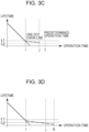
- FIG. 3C corresponds to an example in which the semiconductor device 100 spends the lifetime before the predetermined operation time t when the operation in the normal driving mode continues after time i. That is, the result of determination whether Lt > 0 is satisfied is No in a process at S205.
- FIG. 3C illustrates the relationship between the operation time of the semiconductor device 100 and the remaining lifetime of the semiconductor device 100 by a solid line.
- a dashed line represents an estimated remaining lifetime of the semiconductor device 100 that is estimated by the lifetime estimating unit 109 at time i with respect to the operation time of the semiconductor device 100.
- a one-dot chain line represents a relationship between the operation time of the semiconductor device 100 and the remaining lifetime of the semiconductor device 100 in a changed driving state after the driving state of the semiconductor device 100 is changed at time i.
- the driving mode selecting unit 105 controls the operation of both of the voltage control unit 104 and the frequency control unit 106 or either of them and selects a life-prolonging driving mode in which the remaining lifetime of the semiconductor device 100 is longer than the remaining lifetime at time i.
- the life-prolonging driving mode corresponds to a condition in which the throughput of signal processing is less than that in the case where the semiconductor device 100 is driven in the normal driving mode.
- the driving mode the remaining lifetime of the semiconductor device 100 is longer than that in the case where the semiconductor device 100 is driven in the normal driving mode. That is, the normal driving mode corresponds to a first condition in which the driving control unit drives the semiconductor device 100.
- the life-prolonging driving mode corresponds to a second condition in which the throughput of the signal processing is less than that in the case where the semiconductor device 100 is driven in the first condition and the remaining lifetime of the semiconductor device is longer than that in the case where the semiconductor device 100 is driven in the first condition.
- the state of the operation is changed such that the values of all or a part of the current density J, the temperature T of the wiring line, the voltage Vg that is applied to the gate of the transistor, and the maximum substrate current Isub that flows through the semiconductor substrate are lower than the normal driving mode.
- the change in the state of the operation can be said to be a change for reducing a drive ability through which the semiconductor device 100 is driven.
- the absolute values of the power supply voltages that are supplied to the first circuit block 101, the second circuit block 102, and the N-th circuit block 103 by the voltage control unit 104 are decreased (typically, the power supply voltages are decreased). This enables the current density J, the temperature T of the wiring line, and the voltage Vg to be decreased.
- the temperature T of the wiring line and the substrate current Isub can be decreased by increasing a period in which the signal generating unit 107 generates a signal by using the frequency control unit 106.
- the driving mode selecting unit 105 controls the voltage control unit 104 and the frequency control unit 106 such that the operation of the semiconductor device 100 can continue.
- the semiconductor device 100 In the normal driving mode, the semiconductor device 100 is driven in the first condition as described above. In the life-prolonging driving mode, the semiconductor device 100 is driven in the second condition in which the lifetime of the semiconductor device 100 is longer than that in the case where the semiconductor device 100 continue to be driven in the normal driving mode as described above.
- the amount of the signal processing of the semiconductor device 100 is smaller than that in the normal driving mode, for example, the functions are partly stopped, and the operation speed of the semiconductor device 100 is decreased.
- the life-prolonging driving mode however, the operation of the semiconductor device 100 can continue, and the remaining lifetime can be increased to a lifetime longer than that in the case where the normal driving mode continues in a manner in which a load that is applied to the circuit of the semiconductor device 100 is decreased to a level lower than that in the normal driving mode.
- the throughput of the signal processing of the semiconductor device 100 in the life-prolonging driving mode is less than that in the normal driving mode.
- the throughput of the signal processing corresponds to the quantity of signals on which the semiconductor device 100 performs the signal processing per unit time.
- one or a plurality of the amount of electric current supply from an electric current source, the drive voltage (power supply voltage), and the operating frequency of the semiconductor device 100 in the life-prolonging driving mode is less than in the normal driving mode.
- the signal processing is performed for a first period.
- the life-prolonging driving mode comprises an intermittent drive in which the signal processing is performed for a second period shorter than the first period and signal processing is not performed for a period that is included in the first period and that is not included in the second period, or a drive for reducing the throughput of the signal processing to a level lower than that in the second period.
- the remaining lifetime of the semiconductor device 100 that operates in the life-prolonging driving mode is longer than the second lifetime threshold L2, and subsequent operation in the normal driving mode is possible.
- the lifetime estimating unit 109 calculates the remaining lifetime Lj of the semiconductor device 100 at time j.
- the driving mode selecting unit 105 compares the second lifetime threshold L2 and the remaining lifetime Lj at time j. If Lj > L2 is satisfied, the processing proceeds to S209. If Lj ⁇ L2 is satisfied, the processing proceeds to S210.
- FIG. 3C illustrates the case where Lj > L2 is satisfied.
- the remaining lifetime of the semiconductor device 100 that operates in the life-prolonging driving mode is shorter than the first lifetime threshold L1 and is longer than the second lifetime threshold L2. Accordingly, the semiconductor device 100 has an enough remaining lifetime in the life-prolonging driving mode relative to a predetermined operation continuation period. Accordingly, even when the operation continues for a period not in the life-prolonging driving mode but in the normal driving mode, the semiconductor device 100 can continue the operation until the predetermined operation continuation period. Accordingly, the driving state of the semiconductor device 100 is restored to the normal driving mode before the mode is changed into the life-prolonging driving mode.
- the processing proceeds to S203, and the operation of the semiconductor device 100 continues in the normal driving mode for a freely determined period ⁇ t1. Subsequently, the processing returns to S201.
- FIG. 3D An example in FIG. 3D will now be described.
- a dashed line represents an estimated remaining lifetime of the semiconductor device 100 that is estimated by the lifetime estimating unit 109 at time i with respect to the operation time of the semiconductor device 100.
- a one-dot chain line represents a relationship between the operation time of the semiconductor device 100 and the remaining lifetime of the semiconductor device 100 in a changed driving state after the driving state of the semiconductor device 100 is changed at time i.
- the driving mode selecting unit 105 compares the second lifetime threshold L2 and the remaining lifetime Lj at time j.
- FIG. 3D illustrates the case where Li ⁇ L2 is satisfied.
- the lifetime estimating unit 109 calculates the remaining lifetime Lk of the semiconductor device 100 at time k.
- the driving mode selecting unit 105 determines whether the remaining lifetime Lk at time k is more than 0. If Lk > 0 is satisfied, the processing proceeds to S212. If Lk ⁇ 0 is satisfied, the processing proceeds to S213. According to the present embodiment, the case where the processing proceeds to S212 when Lk > 0 is satisfied will be described.
- the remaining lifetime of the semiconductor device 100 that operates in the life-prolonging driving mode is shorter than the first lifetime threshold L2.
- the remaining lifetime of the semiconductor device 100 is close to 0 but is more than 0. Accordingly, the processing proceeds to S212, and a process of continuing the operation of the semiconductor device 100 for a freely determined period ⁇ t2 is performed.
- the processing returns to S210.
- the period ⁇ t2 that corresponds to an interval in which the remaining lifetime Lk is obtained is set shorter than the period ⁇ t1 that corresponds to an interval in which the remaining lifetime Li is obtained in the case where the remaining lifetime is longer than the first lifetime threshold L1. This enables a time during which a normal operation of the semiconductor device 100 is not guaranteed to be detected with precision.
- FIG. 3E An example in FIG. 3E will now be described.
- FIG. 3E illustrates the case where Lk ⁇ 0 is satisfied.
- the remaining lifetime Lk of the semiconductor device 100 is equal to or less than 0, and the operation is not guaranteed.
- the processing proceeds to S213, and it is reported to the outside that the operation of the semiconductor device 100 is not guaranteed.
- An example of a reporting method is to notify the user of the semiconductor device 100 by using, for example, a display not illustrated in FIG. 1 .
- the report is made to a monitoring system that monitors the semiconductor device 100 via a communication line.
- the processing proceeds to S214, and the operation of the semiconductor device 100 is stopped.
- the remaining lifetime of the semiconductor device 100 is equal to or less than 0 at time k, and the operation of the semiconductor device 100 is not guaranteed. For this reason, it is reported to a location outside the semiconductor device 100 that the operation of the semiconductor device 100 is not guaranteed. The operation of the semiconductor device 100 is stopped.
- the operation is prevented from continuing while the operation is not guaranteed even though the remaining lifetime of the semiconductor device 100 is equal to or less than 0.
- the semiconductor apparatus changes the driving state, based on the remaining lifetime information.
- This enable the semiconductor device 100 to be driven depending on the remaining lifetime.
- the mode is changed from the normal driving mode into the life-prolonging driving mode. This enables the lifetime of the semiconductor device 100 to be prolonged while the operation of the semiconductor device 100 continues.
- the interval in which the remaining lifetime information is obtained is shortened to a level lower than that in the case where the remaining lifetime is more than the first lifetime threshold. This enables the remaining lifetime of the semiconductor device 100 to be obtained with precision. In the case where the remaining lifetime of the semiconductor device 100 is equal to or less than 0, this is reported to a location outside the semiconductor device 100. This prevents the operation from continuing while the operation of the semiconductor device 100 is not guaranteed.
- the driving mode of the semiconductor device 100 is changed depending on whether the remaining lifetime exceeds the first lifetime threshold.
- This example is not a limitation.
- the mode may be changed into the normal driving mode.
- the mode may be changed into the life-prolonging driving mode.
- the semiconductor apparatus includes the lifetime estimating unit 109 but is not limited to this example.
- the semiconductor apparatus may include a time obtaining unit that obtains time information that represents the elapsed time of the operation of the semiconductor device 100. In this case and in the case where the time information corresponds to the first length, the semiconductor device 100 is driven in the first condition. In the case where the time information corresponds to the second length longer than the first length, the semiconductor device 100 is driven in the second condition. In the second condition, the throughput of the signal processing is less than that in the case where the semiconductor device is driven in the first condition, and the remaining lifetime of the semiconductor device is longer than that in the case where the semiconductor device is driven in the first condition.
- an image sensor is used as the semiconductor device 100 according to the first embodiment.
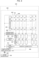
- An image capturing apparatus 450 illustrated in FIG. 4 includes the image sensor and the lifetime estimating unit 109.
- An image sensor 400 is a CMOS sensor.
- a pixel array 402 that includes pixels 401 that are arranged in rows and in columns, a vertical scanning circuit 403, vertical output lines 404, and column circuits 405 is provided.
- the image sensor 400 includes a reference signal generating circuit 406, storage units 407, a counter circuit 408, a horizontal scanning circuit 409, a signal processing circuit 410, an image capturing mode control unit 411, and the lifetime estimating unit 109.
- each pixel 401 will now be described with reference to FIG. 5 .
- Each pixel 401 includes photodiodes 501a and 501b.
- photodiodes 501a and 501b of the single pixel 401 On the photodiodes 501a and 501b of the single pixel 401, light that passes through a single microlens, not illustrated, is incident.
- the photodiodes 501a and 501b receive light from different regions of an exit pupil of an optical system that guides the light to the CMOS sensor. For this reason, the use of a signal based on electric charges that are obtained by photoelectric conversion carried out by the photodiodes 501a and 501b enables focus detection in a phase difference method.
- An image can be generated by using a signal corresponding to an electric charge that is obtained by adding the electric charge that is obtained by the photoelectric conversion carried out by the photodiode 501a and the electric charge that is obtained by the photoelectric conversion carried out by the photodiode 501b.
- the photodiodes 501a and 501b accumulate the electric charges depending on the incident light.
- the vertical scanning circuit 403 illustrated in FIG. 4 performs vertical scanning in which signals are read in a unit of the rows from the pixels 401 that are arranged in the rows.
- the electric charge that is accumulated by the photodiode 501a is transferred to a floating diffusion unit (FD unit) 503 by setting a signal txa that is outputted to a transfer gate 502a at a high level.
- FD unit floating diffusion unit
- the electric charge that is accumulated by the photodiode 501b is transferred to the FD unit 503 in a manner in which the vertical scanning circuit 403 sets a signal txb that is outputted to a transfer gate 502b at a high level.
- the FD unit 503 converts the electric charges that are transferred from the photodiodes 501a and 501b into a voltage, based on the capacity of the FD unit 503.
- the FD unit 503 is connected to a gate of an amplifier transistor 504.
- the amplifier transistor 504 is connected to the vertical output line 404 via a selection transistor 506.
- Each pixel 401 includes a reset transistor 505 that is connected to the FD unit 503.
- the reset transistor 505 resets the FD unit 503 in a manner in which the vertical scanning circuit 403 sets a signal res at a high level.
- the vertical scanning circuit sets the signals txa and txb at a high level in the period in which the signal res is at a high level.
- the signals res, txa, txb, and sel that are supplied from the vertical scanning circuit 403 are inputted into the pixels 401 in a single row in common.
- the outputs vout of the pixels 401 are inputted into the corresponding column circuits 405 via the vertical output lines 404 corresponding to the columns in which the pixels 401 are arranged.
- each column circuit 405 that is arranged for every column will now be described with reference to FIG. 6 .
- FIG. 6 illustrates the structure of each column circuit 405.
- the column circuit 405 includes an electric current source 601, a switch 602, a differential amplifier 603, a switch 604, a comparator 605, and a switch 606.
- the switch 602 switches between on and off of the electric current source 601.
- the switch 604 switches between on and off of the differential amplifier 603.
- the switch 606 switches between on and off of the comparator 605.
- the vertical scanning circuit 403 sets a signal sel that is supplied to the pixel 401 in the row to be read at a high level. Consequently, an electric current flows between the amplifier transistor 504 and the electric current source 601 via the selection transistor 506 of the pixel 401 in the row to be read. Consequently, the amplifier transistor 504 performs a source follower operation. Consequently, a signal (pixel signal) based on the voltage of the FD unit 503 is outputted to the vertical output line 404.
- the differential amplifier 603 When the switch 604 is on, the differential amplifier 603 operates. In this case, the differential amplifier 603 outputs, to the comparator 605, an amplified signal that is obtained by amplifying the pixel signal that is outputted from the pixel 401 to the vertical output line 404.
- the comparator 605 When the switch 606 is on, the comparator 605 operates. In this case, the comparator 605 compares the voltage of the amplifier signal that is outputted from the differential amplifier 603 and the voltage of a ramp signal that is supplied from the reference signal generating circuit 406. The comparator 605 outputs, as a signal Cout, the result of comparison to each storage unit 407 illustrated in FIG. 4 . The signal level of the signal Cout changes when a relationship in the magnitude of the signal voltage is inverted. A count signal is inputted into the storage unit 407 from the counter circuit 408. The count signal changes a count value in response to a timing with which the voltage of the ramp signal that is supplied from the reference signal generating circuit 406 starts changing.
- the storage unit 407 latches the count value, based on a timing with which the signal level of the signal Cout changes. This enables the storage unit 407 to obtain digital data corresponding to the signal level of the amplifier signal. In this way, the column circuit 405 and the storage unit 407 carry out AD conversion of the pixel signal.
- the digital data that is stored in the storage unit 407 is sequentially transferred to the signal processing circuit 410 by using the horizontal scanning circuit 409 for every column.
- a series of operations in relation to readout of the pixel signals from the pixels are performed while a pixel row of the pixel array 402 is selected by the vertical scanning circuit 403.
- FIGs. 7A and 7B are timing diagrams illustrating the operation of the image capturing apparatus illustrated in FIG. 6 .
- FIG. 7A is a timing diagram in the case where an image capturing operation is performed.
- FIG. 7B is a timing diagram in the case where a focus detection operation and the image capturing operation are performed.
- the pixel signals are read out from pixels 401 included in a part of the rows among the pixels 401 in the rows that are arranged in the pixel array 402 by performing the image capturing operation and the focus detection operation illustrated in FIG. 7B .
- the pixel signals are read out from pixels 401 included in another part of the rows by performing the image capturing operation illustrated in FIG. 7A .
- the part of the rows and the other part of the rows are assigned depending on a region in which the focus detection is made.
- the pixels 401 in all of the rows perform the operation in FIG. 7A for a certain frame.
- the operation in FIG. 7B may be performed for another frame.
- the frame described in this case may correspond to, for example, a period from when the vertical scanning circuit 403 starts vertical scanning until when the next vertical scanning is started.
- the frame can typically correspond to a period in which a control circuit, not illustrated, sets the signal level of a vertical synchronization signal for instructing the start of vertical scanning of the vertical scanning circuit 403 at a high level and subsequently sets the signal level of a vertical synchronization signal at a high level.
- the frame can also correspond to a period from the starts of reading a signal corresponding to one image that is generated by a signal processing unit from the pixel array 402 to the starts of reading a signal corresponding to the next one image from the pixel array 402.
- a video is shot at 60 fps (fps is an abbreviation for frames per second).
- the frame can correspond to a period in which a signal corresponding to an image of one frame of 60 frames starts to be read out from the pixel array 402, and a signal corresponding to an image of a next one frame subsequently starts to be read out from the pixel array 402.
- the vertical scanning circuit 403 sets the signal sel that is supplied to the row of the pixel 401 that performs the image capturing operation at a high level. Consequently, the selection transistor 506 of the pixel 401 is turned on.
- the vertical scanning circuit 403 sets the signal res at a low level and turns the reset transistor 505 off. Consequently, the reset of the FD unit 503 is released.
- the amplifier transistor 504 outputs a noise signal (N signal) based on the voltage of the FD unit 503 the reset of which is released to the vertical output line 404 via the selection transistor 506.
- the N signal that is outputted to the vertical output line 404 is converted into digital data (N data) by AD conversion carried out by the column circuit 405 and the storage unit 407.
- the vertical scanning circuit 403 sets the signals txa and txb at a high level and subsequently sets the signals txa and txb at a low level.
- the electric charge that is accumulated based on the incident light by the photodiode 501a and the electric charge that is accumulated based on the incident light by the photodiode 501b are transferred to the FD unit 503.
- the voltage of the FD unit 503 corresponds to the electric charge that is obtained by adding the electric charge of the photodiode 501a and the electric charge of the photodiode 501b.
- the amplifier transistor 504 outputs a signal based on the voltage of the FD unit 503 that corresponds to the electric charge that is obtained by adding the electric charge of the photodiode 501a and the electric charge of the photodiode 501b, to the vertical output line 404 via the selection transistor 506.
- the signal that is outputted by the amplifier transistor 504 will be described. If the voltage of the FD unit 503 is based on the electric charge that is accumulated based on the incident light by the photodiode 501a, the signal that is outputted by the amplifier transistor 504 is referred to as an A + N signal (the sum of an A signal and the N signal).
- the signal that is outputted by the amplifier transistor 504 is referred to as a B + N signal (the sum of a B signal and the N signal).
- the signal that is outputted by the amplifier transistor 504 and that is based on the voltage of the FD unit 503 that corresponds to the electric charge that is obtained by adding the electric charge of the photodiode 501a and the electric charge of the photodiode 501b corresponds to a signal that is obtained by adding the A + N signal and the B + N signal.
- the signal that is outputted by the amplifier transistor 504 is referred to as an A + B + N signal.
- the A + B + N signal that is outputted to the vertical output line 404 is converted into digital data (A + B + N data) by AD conversion carried out by the column circuit 405 and the storage unit 407.
- the vertical scanning circuit 403 sets the signal res at a high level. Consequently, the voltage of the FD unit 503 is reset.
- the vertical scanning circuit 403 sets the signal sel at a low level. This is the end of the selection of the pixels 401 in one row. Subsequently, the vertical scanning circuit 403 sets the signal sel of the pixels 401 in the rows for next to be read at a high level.
- the N data and the A + B + N data that are held by the storage unit 407 are sequentially read out from the storage unit 407 into the signal processing circuit 410 by using the horizontal scanning circuit 409 for every column.
- the signal processing circuit 410 outputs A + B data that corresponds to a signal of a difference between the A + B + N data and the N data.
- An operation at time tb1 is the same as an operation at time ta1 in FIG. 7A .
- An operation at time tb2 is the same as an operation at time ta2 in FIG. 7A .
- the vertical scanning circuit 403 sets the signal txa at a high level and subsequently sets the signal txa at a low level. Consequently, the electric charge that is accumulated based on the incident light by the photodiode 501a is transferred to the FD unit 503.
- the amplifier transistor 504 outputs the A + N signal to the vertical output line 404 via the selection transistor 506.
- the A + N signal that is outputted to the vertical output line 404 is converted into digital data (A + N data) by AD conversion carried out by the column circuit 405 and the storage unit 407.
- the FD unit 503 holds the electric charge that is transferred from the photodiode 501a until before time tb6.
- the vertical scanning circuit 403 sets the signal txa and the signal txb at a high level and subsequently sets the signal txa and the signal txb at a low level. Consequently, the FD unit 503 holds the electric charge that is accumulated based on the incident light by the photodiode 501b and the electric charge that is accumulated in a period from time tb4 to time tb7 by the photodiode 501a in addition to the electric charge of the photodiode 501a that is held before time tb6. Accordingly, the voltage of the FD unit 503 corresponds to the electric charge that is obtained by adding the electric charge of the photodiode 501a and the electric charge of the photodiode 501b.
- the amplifier transistor 504 outputs the A + B + N signal to the vertical output line 404.
- the A + B + N signal that is outputted to the vertical output line 404 is converted into digital data (A + B + N data) by AD conversion carried out by the column circuit 405 and the storage unit 407.
- the vertical scanning circuit 403 sets the signal res at a high level. Consequently, the voltage of the FD unit 503 is reset.
- the vertical scanning circuit 403 sets the signal sel at a low level. This is the end of the selection of the pixels 401 in one row. Subsequently, the vertical scanning circuit 403 sets the signal sel of the pixel 401 in the row for next to be read at a high level.
- the N data, the A + N data, and the A + B + N data that are held by the storage unit 407 are sequentially read out from the storage unit 407 into the signal processing circuit 410 by using the horizontal scanning circuit 409 for every column.
- the signal processing circuit 410 outputs a signal (A data) of a difference between the A + N data and the N data and a signal of a difference between the A + B + n data and the N data (A + B data).
- the signal processing unit which receives the data that is outputted by the image capturing apparatus obtains B data that corresponds to a difference between the A data and the A + B data and performs the focus detection by using the A data and the B data.
- the signal processing unit generates an image by using the A + B data.
- the image capturing mode control unit 411 is a circuit block that includes the voltage control unit 104, the driving mode selecting unit 105, the frequency control unit 106, and the signal generating unit 107 described according to the first embodiment.
- the image capturing mode control unit 411 receives the remaining lifetime information from the lifetime information receiving unit 108.
- the voltage values that are supplied to all or a part of the circuits in the image sensor 400 or the period of the control signal are changed depending on the remaining lifetime that represents the remaining lifetime information.
- the circuits in the image sensor 400 are the pixel array 402, the vertical scanning circuit 403, the column circuits 405, the reference signal generating circuit 406, the storage units 407, the counter circuit 408, the horizontal scanning circuit 409, and the signal processing circuit 410.
- the operation of a part of the pixel array 402, the vertical scanning circuit 403, the column circuits 405, the reference signal generating circuit 406, the storage units 407, the counter circuit 408, the horizontal scanning circuit 409, and the signal processing circuit 410 in the image sensor 400 is stopped.
- the lifetime of the semiconductor apparatus is limited by the current density J of the wiring line, the temperature T of the wiring line, the voltage Vg that is applied to the gate of the transistor, and the maximum substrate current Isub that flows through the semiconductor substrate.
- the image capturing mode control unit 411 changes the state of the operation such that all or a part of the current density J, the temperature T of the wiring line, the voltage Vg that is applied to the gate of the transistor, and the maximum substrate current Isub that flows through the semiconductor substrate decrease in order to prolong the remaining lifetime of the image sensor 400.
- the throughput of the signal processing of the image capturing apparatus is reduced, for example, the speed of the operation is decreased or the functions are partly stopped.
- the lifetime of the image capturing apparatus can be increased.
- the frame rate decreases. Specifically, the period of the vertical scanning of the vertical scanning circuit 403 decreases relative to the normal driving mode. The decrease in the period of the vertical scanning results in decreases in the operation periods of the reference signal generating circuit 406, the counter circuit 408, the horizontal scanning circuit 409, and the signal processing circuit 410. It can also be said that a decrease in the frame rate means a decrease in the number of times the vertical scanning circuit 403 performs the vertical scanning per unit time.
- signals may be read out from the pixels 401 in a region of a part of the pixel array 402. That is, the number of the pixels that are read out in the life-prolonging driving mode is smaller than that in the normal driving mode.
- the pixels 401 suitable for a resolution of 4K2K are read in the normal driving mode
- the pixels 401 suitable for a resolution of VGA are read in the life-prolonging driving mode.
- the horizontal scanning circuit 409 scans the storage units 407 in a part of the columns. Consequently, while the operation of the image capturing apparatus continues, the remaining lifetime of the image capturing apparatus can be prolonged.
- This example is one of the examples in which the throughput of the signal processing of the image capturing apparatus is reduced.
- the number of the pixels that perform the focus detection operation in FIG. 7B in the life-prolonging driving mode may be less than that in the normal driving mode. Consequently, the number of times that the AD conversion of the A + N signal is carried out by the column circuits 405 and the storage units 407 can be decreased. Consequently, while the image capturing operation continues, the remaining lifetime of the image capturing apparatus can be prolonged. In particular, in the case where an extension in the remaining lifetime is considered to be important, no pixels perform the focus detection operation in FIG. 7B , and all of the pixels 401 carries out drive of the image capturing operation in FIG. 7A .
- This example is one of the examples in which the throughput of the signal processing of the image capturing apparatus is reduced.
- the lifetime estimating unit 109 obtains the remaining lifetime information on the image sensor 400 by estimating the remaining lifetime of the image sensor 400, based on the latest state of the operation of the image sensor 400 or the history information in relation to the state of the operation as described according to the first embodiment.
- the state of the operation means a state in which the image sensor 400 operates such as an operation voltage or an operating frequency at which the image sensor 400 operates or a state caused as a result of the operation such as a temperature.
- the lifetime estimating unit 109 obtains the remaining lifetime information after the image capturing operation is performed multiple times.
- the image capturing operation described herein means an operation for imaging an object in various environments. That is, the image capturing operation does not mean the image capturing operation of the image sensor 400 in a known environment such as a test in a manufacturing factory of an image capturing apparatus but means an image capturing operation in an environment in which the remaining lifetime of the image sensor 400 changes due to the environment in which the image sensor 400 is disposed. Accordingly, the image capturing apparatus according to the present embodiment can estimate the remaining lifetime depending on a previous environment or a current environment in which the image sensor 400 is actually disposed and the operation. Since the remaining lifetime is estimated based on the previous environment or the current environment in which the image sensor 400 is actually disposed, the remaining lifetime can be estimated more accurately than the lifetime is estimated in a simulation.
- drive for prolonging the lifetime of the image sensor 400 is selected based on the remaining lifetime information. This solves a problem in that the image sensor 400 spends the lifetime earlier than a service life.
- the image capturing apparatus can be used, for example, as a camera that is disposed in an area in which it is difficult to replace the image capturing apparatus.
- the camera include cameras (disaster monitoring (a volcanic disaster and a meteorological disaster) that are disposed in remote areas and monitoring cameras that are disposed in a space ship, an artificial satellite (such as a weather observation satellite, an exploration satellite, or a space station), and a space exploration robot), and monitoring cameras that are disposed in conflict areas.
- the image capturing apparatus is not easy to replace even after the lifetime, and it is desired that the operation of the image capturing apparatus continues.
- the operation of the image sensor 400 is changed from that in the normal driving mode to that in the life-prolonging driving mode. Consequently, while the image capturing operation continues, the remaining lifetime of the operation of the image capturing apparatus can be prolonged.
- the image capturing apparatus according to the present embodiment can be used as a vehicle-mounted camera that is taken as an example of the image capturing apparatus that is mounted on a moving object.
- the image sensor 400 is not easy to replace during driving even when the remaining lifetime is shorter than the first lifetime threshold. In this case, it is useful that the normal driving mode is changed into the life-prolonging driving mode, the image capturing operation of the image sensor 400 continues, and the lifetime of the image sensor 400 is increased.
- the lifetime estimating unit 109 obtains the remaining lifetime information in parallel with the image capturing operation. For example, in the case of a camera that is disposed in a remote area or a camera that continuously shoots a video such as a monitoring camera, the lifetime estimating unit 109 obtains the remaining lifetime information in a period in which the image capturing operation is performed. Consequently, while the video is continuously shot, the remaining lifetime of the image sensor 400 can be estimated. In other words, the lifetime estimating unit 109 may obtain the remaining lifetime information in a period in which vertical scanning is performed. The lifetime estimating unit 109 may obtain the remaining lifetime information in a period in which the photoelectric converters accumulate electric charges based on the incident light.
- the lifetime estimating unit 109 may obtain the remaining lifetime information in a period (for example, a period in which AD conversion is carried out) in which the column circuits 405 and the storage units 407 process the pixel signals. That is, after the image capturing operation is performed multiple times, the lifetime estimating unit 109 may obtain the remaining lifetime information in parallel with the period in which the image capturing operation is performed.
- the image capturing apparatus enables the lifetime of the image sensor to be prolonged while continuing the operation of the image sensor.
- the image capturing apparatus according to the present embodiment can obtain the remaining lifetime information on the image sensor with precision.
- FIG. 8 illustrates an image capturing apparatus 800 according to the present embodiment.
- the image capturing apparatus 800 differs from the image capturing apparatus 450 illustrated in FIG. 4 in including a state obtaining unit 812 and a lifetime estimating unit 813 that is connected to the state obtaining unit 812.
- the following description includes the case where hot carrier injection (HC) is dominant regarding a factor in the impairment in the performance of the image sensor 400.
- the state obtaining unit 812 measures the drain current Id of the transistor of the image sensor 400. The result of measurement is outputted to the lifetime estimating unit 813.
- the lifetime estimating unit 813 calculates a ratio of a variation in the latest drain current Id of a MOS transistor to the known initial drain current Id of the MOS transistor.
- the lifetime estimating unit 813 sets a threshold for the IdRATIO to 10%.
- the lifetime estimating unit 813 estimates the remaining lifetime of the image sensor 400 by comparing a threshold of 10% and the actual IdRATIO.
- a resistance element is disposed in the state obtaining unit 812, an end of the resistance element is connected to the power supply voltage, and the other end of the resistance element is connected to the drain of the transistor of the image sensor 400.
- V IR
- a variation in electric power consumption of the image sensor 400 may be measured.
- the drain current Id of the transistor can be indirectly measured by measuring a variation between the electric power consumption at measurement and the electric power consumption of the image sensor 400 when the image sensor is a new product.
- the remaining lifetime can be estimated by obtaining a variation in the electric power consumption over time.
- An image capturing apparatus according to the present embodiment, mainly differences from the third embodiment will be described.
- the structure of the image capturing apparatus can be the same as that in FIG. 8 .
- the image capturing apparatus estimates the remaining lifetime by using the variation in the drain current Id. According to the present embodiment, another estimating method will be described.
- the performance of the semiconductor device and the image sensor impairs due to the HC, the EM, the TDDB, or the negative NBTI as described according to the first embodiment.
- the lifetimes of the semiconductor device and the image sensor are determined by the impairment in the performance.
- Lifetime estimation in relation to the impairment in the performance due to the HC is described according to the third embodiment.
- a lifetime LT (EM) when the factor in the impairment in the performance is the EM is obtained by using expression (1) described according to the first embodiment.
- a lifetime LT (TDDB) when the factor in the impairment in the performance is the TDDB is obtained by using expression (2) according to the first embodiment.
- a lifetime LT (NBTI) when the factor in the impairment in the performance is the NBTI can be calculated by using expression (4) described according to the first embodiment.
- a lifetime LT (HC) when the factor in the impairment in the performance is the HC is obtained by using expression (3) described according to the first embodiment and is also obtained by using expression (5) described according to the third embodiment.
- the state obtaining unit 812 performs measurement of all or a part of expression (1) to expression (5) and calculates the lifetime of the image sensor 400.
- the state obtaining unit 812 measures the current density J of the electric current that flows through the transistor or the resistance element that is included in the image sensor 400, the temperature T of the wiring line, and the voltage value Vg that is applied to the gate of the transistor.
- a method of obtaining the current density J is the same as that according to the third embodiment.
- the value of an electric current that flows through a diode element, not illustrated, of the state obtaining unit 812 is measured.
- the value of the electric current that flows through the diode element typically depends on the temperature. Accordingly, the temperature T can be obtained by measuring the value of the electric current.
- the voltage value Vg can be a gate voltage that is applied to the transistor the lifetime of which is to be estimated. In the case where it can be expected that a difference between a measured value and a design value can be substantially ignored, the voltage value Vg may be the designed value.
- the state obtaining unit 812 thus obtains the values that are used in expression (1) to expression (5).
- the state obtaining unit 812 outputs the obtained values to the lifetime estimating unit 813. That is, the state obtaining unit 812 obtains the electric current consumption and the temperature of the image sensor 400.
- the state obtaining unit 812 may further obtain information about the frame rate and the cumulative time of the operation of the image sensor 400.
- the lifetime estimating unit 813 obtains the lifetime of the image sensor 400 by using all or a part of expression (1) to expression (5). In the case where the lifetime is estimated by using multiple expressions among expression (1) to expression (5), the lifetime estimating unit 813 sets the lifetime of the image sensor 400 to the minimum lifetime among those obtained by the used expressions.
- the lifetime estimating unit 813 thus estimates a lifetime based on the actual state of the operation of the image sensor 400. Consequently, the lifetime can be estimated with precision.
- the lifetime of the image sensor 400 greatly varies depending on an usage environment.
- the lifetime varies depending on the temperature at which the image sensor 400 is disposed, the number of times of shooting, and a supplied voltage. For example, a time during which the vehicle-mounted camera is left at a high temperature of 80°C or more in a low latitude area is longer than that in a high latitude area. A time during which the vehicle-mounted camera is left at a low temperature of 0°C or less in the high latitude area is longer than that in the low latitude area. Accordingly, the actual lifetime of the image sensor 400 can be shorter than a designed lifetime. Consequently, lifetime estimation based on the actual operation of the image sensor 400 enables the operation of the image sensor 400 to be unlikely to stop suddenly.
- the state obtaining unit 812 and the lifetime estimating unit 813 are disposed outside the image sensor 400.
- the state obtaining unit 812 and the lifetime estimating unit 813 may be disposed inside the image sensor 400.
- the state obtaining unit 812 is disposed on the same semiconductor substrate as the image sensor 400, the state obtaining unit 812 is disposed in the same operation environment as the image sensor 400, and the lifetime can be estimated with more precision.
- FIG. 9 illustrates the structure of the image capturing apparatus according to the present embodiment.
- the image capturing apparatus according to the present embodiment further includes a memory 920 relative to the image capturing apparatus according to the fourth embodiment.
- the memory 920 holds the history information in relation to the state of the operation.
- a lifetime estimating unit 913 estimates the remaining lifetime by using the history information that is held by the memory 920 and information that is outputted from the state obtaining unit 812 and generates the remaining lifetime information.
- the history information include a history of the image capturing mode of the image capturing apparatus and the cumulative time of the operation of the image capturing apparatus.
- the image capturing mode includes a period (frame rate) in which the image sensor 400 outputs an image signal, an image size, and whether the focus detection function is performed.
- the remaining lifetime that is estimated by the lifetime estimating unit 913 by using all or a part of expression (1) to expression (5) as described according to the fourth embodiment is corrected by using the history information that is held by the memory 920.
- the memory 920 holds the IdRATIO that is obtained by using expression (5) whenever the remaining lifetime is estimated.
- the lifetime estimating unit 913 obtains the variation in the IdRATIO over time by using the IdRATIO at each time that is held by the memory 920. From the variation in the IdRATIO over time, time at which the IdRATIO becomes 10% or more is estimated (that is, the remaining lifetime is estimated). Consequently, the remaining lifetime can be estimated with more precision.
- Values that are stored in the memory 920 are not limited to the drain current Id of the transistor but may be values in all or a part of expression (1) to expression (5).
- the memory 920 may be located outside the image capturing apparatus 800.
- the memory 920 is preferably a non-volatile memory. In the case where the memory 920 is disposed outside the image capturing apparatus 800, processing of manufacturing the image capturing apparatus 800 and the memory 920 can be divided. Consequently, restrictions on a process of manufacturing the image capturing apparatus 800 and a process of manufacturing the memory 920 can be decreased.
- the image capturing apparatus thus includes the memory 920 that holds the history information in relation to the state of the operation.
- the remaining lifetime can be estimated with precision by using the history information that is held by the memory 920.
- Each image capturing apparatus described according to the above embodiments can be a multi-layer type sensor in which chips are stacked.
- a first chip may include the pixel array 402, and a second chip may include the column circuits 405, the reference signal generating circuit 406, the storage units 407, the counter circuit 408, the horizontal scanning circuit 409, the signal processing circuit 410, and the image capturing mode control unit 411.
- the second chip may further include the lifetime estimating unit 109.
- a third chip that includes a signal processing unit that generates an image may also be stacked.
- the third chip may include the lifetime estimating unit 109.
- FIG. 10 is a block diagram illustrating the structure of an image capturing system 500 according to the present embodiment.
- the image capturing system 500 according to the present embodiment includes an image capturing apparatus 200 that has the same structure as one of the image capturing apparatuses according to the above embodiments.
- Specific examples of the image capturing system 500 include a digital still camera, a digital camcorder, and a monitoring camera.
- FIG. 10 illustrates an example of the structure of a digital still camera that uses one of the image capturing apparatuses according to the above embodiments as the image capturing apparatus 200.
- the image capturing system 500 illustrated in FIG. 10 by way of example includes the image capturing apparatus 200, a lens 5020 that images an optical image of the object on the image capturing apparatus 200, an aperture stop 5040 that enables the amount of light that passes through the lens 5020 to be variable, and a barrier 5060 that protects the lens 5020.
- the lens 5020 and the aperture stop 5040 are optical systems that focus light on the image capturing apparatus 200.
- the image capturing system 500 also includes a signal processing unit 5080 that processes an output signal that is outputted from the image capturing apparatus 200.
- the signal processing unit 5080 corrects and compresses an input signal in various ways as needed and performs output-signal processing.
- the signal processing unit 5080 may have a function of carrying out AD conversion of the output signal that is outputted from the image capturing apparatus 200. In this case, an AD conversion circuit is not necessarily included inside the image capturing apparatus 200.
- the image capturing system 500 also includes a buffer memory 510 in which image data is temporarily stored and an external interface (external I/F) 512 for communication with, for example, an external computer.
- the image capturing system 500 also includes a recording medium 514 such as a semiconductor memory that is used to record or read image capturing data and a recording medium control interface (recording medium control I/F) 516 that is used for recording to or reading from the recording medium 514.
- the recording medium 514 may be contained in the image capturing system 500 and may be removable and installable.
- the image capturing system 500 also includes an overall control-calculation unit 518 that makes various kinds of calculations and controls the entire digital still camera and a timing generating unit 520 that outputs a various kinds of timing signals to the image capturing apparatus 200 and the signal processing unit 5080.
- the timing signals may be inputted from the outside. It is only necessary for the image capturing system 500 to include at least the image capturing apparatus 200, the signal processing unit 5080 that processes the output signal that is outputted from the image capturing apparatus 200.
- the overall control-calculation unit 518 and the timing generating unit 520 may perform a part or the whole of the control function of the image capturing apparatus 200.
- the image capturing apparatus 200 outputs an image signal to the signal processing unit 5080.
- the signal processing unit 5080 performs predetermined signal processing on the image signal that is outputted from the image capturing apparatus 200 and outputs image data.
- the signal processing unit 5080 generates an image by using the image signal.
- the integrated circuit 703 is used for the image capturing system and includes an image processing unit 704 that includes a memory 705, an optical distance measuring unit 706, a parallax calculation unit 707, an object recognition unit 708, and an anomaly detection unit 709.
- the image processing unit 704 performs image processing such as a development process or defect correction on the output signals of the image preprocessing units 715.
- the memory 705 stores first record of a captured image and the position of a defect of an imaging pixel.
- the optical distance measuring unit 706 is used for focus on the object and distance measurement.
- the parallax calculation unit 707 calculates parallax (phase difference of a parallax image) from multiple image data that is obtained by the image capturing apparatuses 702.
- the object recognition unit 708 recognizes the subject such as a car, a road, a sign, or a person.
- the anomaly detection unit 709 reports anomaly to a main control unit 713 when detecting the anomaly of the image capturing apparatuses 7
- the integrated circuit 703 may be built with an exclusively designed hardware, may be built with a software module, or may be built with a combination thereof. Alternatively, the integrated circuit 703 may be built with, for example, a FPGA (Field Programmable Gate Array) or an ASIC (Application Specific Integrated Circuit) or may be built with a combination thereof.
- FPGA Field Programmable Gate Array
- ASIC Application Specific Integrated Circuit
- the image capturing system 701 is connected to the vehicle sensor 710 and can detect a state of a vehicle that is running such as a vehicle speed, a yaw rate, and a steering angle, and states of an environment outside the vehicle, another vehicle, or an obstacle.
- the vehicle sensor 710 also functions as a distance information obtaining unit that obtains information about a distance to the object based on the parallax image.
- the image capturing system 701 is connected to a driving assistance control unit 711 that assists a driving in various ways such as automatic steering, automatic cruising, and a function of preventing a collision.
- a collision determination function whether a vehicle collides with another vehicle or an obstacle is presumed, and whether the vehicle collides is determined, based on the result of detection of the image capturing system 701 or the vehicle sensor 710. Consequently, in the case where the collision is presumed, avoidance control is started, and a safety device is activated in the collision.
- the image capturing system 701 is also connected to an alarm device 712 that gives an alarm to the driver, based on the result of determination of a collision determination unit.
- the main control unit 713 controls the vehicle to avoid colliding or to reduce damage, for example, in a manner in which the brake is applied, an accelerator is released, or an engine output is reduced.
- the alarm device 712 gives an alarm to a user, for example, in a manner in which the alarm is given by using, for example, a voice, alarm information is displayed on a screen of a display of, for example, a car navigation system or a meter panel, or a sheet belt or a steering wheel is vibrated.
- the image capturing system 701 takes a picture of the vicinity of the vehicle, for example, the front or rear thereof.
- FIG. 11B illustrates an example of the arrangement of the image capturing system 701 in the case where the image capturing system 701 takes the picture of the front of the vehicle.
- the two image capturing apparatuses 702 are disposed at the front of a vehicle 700. Specifically, the two image capturing apparatuses 702 are disposed symmetrically with each other with respect to a symmetric axis that coincides with a center line that extends in a direction in which the vehicle 700 runs forwards or backwards or a center line of an external shape (for example, the width of the vehicle). This is preferable when information about the distance between the vehicle 700 and the object is obtained or the possibility of a collision is determined.
- the image capturing apparatuses 702 are preferably disposed at positions at which the view of the driver is not obstructed when the driver sights circumstances outside the vehicle 700 from a driver's seat.
- the alarm device 712 is preferably disposed at a position at which the driver easily sees the alarm device 712.
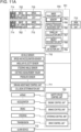
- Failure detecting operation of the image capturing apparatuses 702 of the image capturing system 701 will now be described with reference to FIG. 12 .
- the failure detecting operation of the image capturing apparatuses 702 is performed through steps S810 to S880 illustrated in FIG. 12 .
- the configurations of the image capturing apparatuses 702 during a startup process are set. That is, the configurations for the operation of the image capturing apparatuses 702 are transmitted from a location (for example, the main control unit 713) outside the image capturing system 701 or inside the image capturing system 701, and the image capturing operation and the failure detecting operation of the image capturing apparatuses 702 are started.
- a location for example, the main control unit 713
- step S820 pixel signals are obtained from effective pixels.
- step S830 output values are obtained from failure detecting pixels that are disposed for detecting failure.
- the failure detecting pixels include respective photoelectric converters as in the effective pixels. A predetermined voltage is stored in the photoelectric converters. The failure detecting pixels output signals corresponding to the voltage stored in the photoelectric converters. The order of the step S820 and the step S830 may be inverted.
- step S840 whether expected output values of the failure detecting pixels match the actual output values from the failure detecting pixels is determined.
- step S840 determines whether the result of determination at step S840 is that the expected output values match the actual output values. If the result of determination at step S840 is that the expected output values match the actual output values, the processing proceeds to step S850, in which determination that the image capturing operation is normal is made, and the processing proceeds to step S860.
- step S860 the pixel signals in a scan row are transmitted to the memory 705 and are temporarily stored therein. Subsequently, the processing returns to step S820, and the failure detecting operation continues.
- step S840 determination that the image capturing operation is abnormal is made, and an alarm is given to the main control unit 713 or the alarm device 712.
- the alarm device 712 displays detection of anomaly on the display.
- step S880 the image capturing apparatuses 702 are stopped, and the operation of the image capturing system 701 ends.
- An example described according to the present embodiment illustrates that the flowchart is looped for every row.
- the flowchart may be looped for every set of rows.
- the failure detecting operation may be performed for every frame.
- the alarm may be given to a location outside the vehicle via a wireless network.
- the control described according to the present embodiment is exerted to avoid a collision with another vehicle.
- the present embodiment can be used to control automatic driving for following another vehicle or to control automatic driving for preventing the vehicle from moving out of a lane.
- the image capturing system 701 is not limited to the vehicle such as a car and can be used control automatic driving for following another vehicle or to control automatic driving for preventing the vehicle from moving out of a lane.
- the image capturing system 701 is not limited to the vehicle such as a car and can be used for a moving object (moving device) such as a ship, an aircraft, or an industrial robot. In addition to the moving object, the image capturing system 701 may be used for instrument used for recognizing objects in a wide range such as an intelligent transport system (ITS).
- ITS intelligent transport system
- embodiments of the present disclosure include an embodiment of a combination of a part of one of the above embodiments and the other embodiment, and an embodiment that is obtained by replacing a part of one of the above embodiments with a part of the other embodiment.
Landscapes
- Engineering & Computer Science (AREA)
- Physics & Mathematics (AREA)
- General Physics & Mathematics (AREA)
- Multimedia (AREA)
- Signal Processing (AREA)
- Transportation (AREA)
- Mechanical Engineering (AREA)
- Chemical & Material Sciences (AREA)
- Combustion & Propulsion (AREA)
- Optics & Photonics (AREA)
- Biomedical Technology (AREA)
- General Health & Medical Sciences (AREA)
- Health & Medical Sciences (AREA)
- Transforming Light Signals Into Electric Signals (AREA)
Description
- The present invention relates to an image capturing apparatus, an image capturing system, and a moving object.
- In recent years, various kinds of semiconductor apparatuses have been used. As the operation period of a semiconductor apparatus increases, a loss of the function of the semiconductor apparatus is more likely to occur.
- For example, as for a technique disclosed in the document
JP 2017-173242 A JP 2017-173242 A - In the technique disclosed in the document
JP 2017-173242 A - Further background art is known as follows:
The documentUS 2015/377955 A1 discloses an apparatus and a method for a user configurable reliability control loop. Therein, it is taught that a processor comprises: a reliability meter to track accumulated stress on components of the processor based on measured processor operating conditions; and a controller to receive stress rate limit information from a user or manufacturer and to responsively specify a set of N operating limits on the processor in accordance with the accumulated stress and the stress rate limit information; and performance selection logic to output one or more actual operating conditions for the processor based on the N operating limits specified by the controller. - The document
US 2017/277455 A1 discloses a semiconductor device, a monitoring system, and a lifetime prediction system/method enabling it to notify a user that a semiconductor device is likely to become faulty, before the semiconductor device becomes faulty. Therein, it is taught that a semiconductor device includes functional units and a lifetime prediction circuit, wherein the lifetime prediction circuit acquires a deterioration degree indicating a degree of how each functional unit deteriorates, using a signal that is output from each functional unit, and the lifetime prediction circuit executes processing to make a notification that the semiconductor device is close to its lifetime, if the deterioration degree is more than a first threshold. - Further documents of relevant background art are e.g.
US 2008/036487 A1 ,US 2009/287909 A1 andUS 2009/254287 A1 . - According to the present invention, drive for increasing the remaining lifetime of an image capturing apparatus is considered.
- The present invention has been accomplished in view of the above problem. Accordingly, the present invention provides an image capturing apparatus, an image capturing system, and a moving object, as defined by the claims.
- According to the present invention, the remaining lifetime of an image capturing apparatus can be increased.
- Also, according to the present invention, an image capturing apparatus that can estimate remaining lifetime after an image capturing operation is actually performed is provided.
-
-
FIG. 1 illustrates the structure of a semiconductor apparatus according to an embodiment which is not part of but useful for understanding the present invention. -
FIG. 2 is a flowchart illustrating the operation of the semiconductor apparatus. -
FIG. 3A illustrates a relationship between the operation time and the lifetime of the semiconductor apparatus. -
FIG. 3B illustrates a relationship between the operation time and the lifetime of the semiconductor apparatus. -
FIG. 3C illustrates a relationship between the operation time and the lifetime of the semiconductor apparatus. -
FIG. 3D illustrates a relationship between the operation time and the lifetime of the semiconductor apparatus. -
FIG. 3E illustrates a relationship between the operation time and the lifetime of the semiconductor apparatus. -
FIG. 4 illustrates the structure of an image capturing apparatus according to an embodiment of the present invention. -
FIG. 5 is an equivalent circuit diagram of a pixel. -
FIG. 6 a block diagram of a column circuit. -
FIG. 7A illustrates the operation of the image capturing apparatus. -
FIG. 7B illustrates the operation of the image capturing apparatus. -
FIG. 8 illustrates the structure of an image capturing apparatus according to an embodiment of the present invention. -
FIG. 9 illustrates the structure of an image capturing apparatus according to an embodiment of the present invention. -
FIG. 10 illustrates the structure of an image capturing system according to an embodiment of the present invention. -
FIG. 11A illustrates the structure of a moving object according to an embodiment of the present invention. -
FIG. 11B illustrates the structure of the moving object. -
FIG. 12 illustrates the operation of an image capturing system according to an embodiment of the present invention. - Embodiments of the present disclosure will hereinafter be described with reference to the drawings. The first embodiment is useful for understanding the invention, but falls outside the scope of the claims.
- In the following description, a transistor is an N-type transistor, provided that there is no notification. However, the embodiments described below are not limited to an N-type transistor, a P-type transistor may be appropriately used. In this case, the voltage of a gate, a source, and a drain of the transistor can be appropriately changed from those in the description according to the embodiments. For example, in the case of a transistor that operates as a switch, the low level and the high level of a voltage that is applied to the gate are inverted in comparison with the description according to the embodiments.
-
FIG. 1 illustrates an example of the structure of a semiconductor apparatus according to the present embodiment. Asemiconductor apparatus 150 includes asemiconductor device 100 and a lifetime estimatingunit 109. Thesemiconductor device 100 is a circuit that has many functions such as light reception, light emission, AD conversion processing, signal processing, communication processing, a storage unit, and a detection unit. The structure and the operation of thesemiconductor device 100 will now be described. - A
first circuit block 101, asecond circuit block 102, and a N-th circuit block 103 are circuits that have many functions such as light reception, light emission, AD conversion processing, signal processing, communication processing, a storage unit, and a detection unit. - A
voltage control unit 104 supplies, to thefirst circuit block 101, thesecond circuit block 102, and the N-th circuit block 103, a voltage value that is set by using a signal from a drivingmode selecting unit 105 that corresponds to a driving control unit. - When the voltage value that is supplied by the
voltage control unit 104 is zero, all or a part of thefirst circuit block 101, thesecond circuit block 102, and the N-th circuit block 103 are turned off. - By using the signal from the driving
mode selecting unit 105, afrequency control unit 106 changes a period in which asignal generating unit 107 generates control signals that are to be transmitted to thefirst circuit block 101, thesecond circuit block 102, and the N-th circuit block 103. - The driving
mode selecting unit 105 receives remaining lifetime information from thelifetime estimating unit 109 that corresponds to a lifetime obtaining unit described later via a lifetimeinformation receiving unit 108. Thevoltage control unit 104 and thefrequency control unit 106 are controlled depending on the information. The drivingmode selecting unit 105 can generate a control signal that enables all or a part of thefirst circuit block 101, thesecond circuit block 102, and the N-th circuit block 103 to be stopped. - The
lifetime estimating unit 109 estimates the lifetime of thesemiconductor device 100, based on information that represents the latest state of the operation of thesemiconductor device 100 or history information in relation to the state of the operation and obtains the remaining lifetime information on thesemiconductor device 100. That is, thelifetime estimating unit 109 corresponds to the lifetime obtaining unit that obtains the lifetime information. The state of the operation means a state in which thesemiconductor device 100 operates such as an operation voltage or an operating frequency at which thesemiconductor device 100 operates or a state caused as a result of the operation such as a temperature. The information that represents the latest state of the operation of thesemiconductor device 100 and the history information in relation to the state of the operation are operation information that represents the state of the operation of thesemiconductor device 100. - An example of a method of estimating the lifetime of the
semiconductor device 100 that is performed by thelifetime estimating unit 109 will now be described. The lifetime of the semiconductor apparatus is typically limited because the performance of a transistor, a wiring line, and an oxide film that are included in the semiconductor apparatus impairs over time. Main mechanisms of the impairment in the performance of the semiconductor apparatus include electromigration (EM) and time dependent dielectric breakdown (TDDB). Other mechanisms of the impairment in the performance include variations in characteristics due to hot carrier injection (HC) and negative bias temperature instability (NBTI). - A remaining lifetime LT (EM) when a factor in the impairment in the performance is EM is calculated by using the following expression (1):

- Here, A is a coefficient that depends on a manufacturing process, Ea is an activation energy, J is the current density of the wiring line, n is a current acceleration factor, k is the Boltzmann constant, and T is the temperature of the wiring line.
- A remaining lifetime LT (TDDB) when the factor in the impairment in the performance is TDDB is calculated by using the following expression (2):

- Here, Vg is a voltage that is applied to the gate of the transistor, and yVg is a voltage acceleration factor.
- A remaining lifetime LT (HC) when the factor in the impairment in the performance is HC is calculated by using the following expression (3):

- Here, Isub is the maximum substrate current that flows through a semiconductor substrate, and m is a coefficient that depends on the substrate current.
- A remaining lifetime LT (NBTI) when the factor in the impairment in the performance of the
semiconductor device 100 is NBTI is calculated by using the following expression (4):
- The
lifetime estimating unit 109 measures all or a part of coefficients in expression (1) to expression (4) and calculates the remaining lifetime of thesemiconductor device 100. Thelifetime estimating unit 109 may be located inside thesemiconductor device 100. - Examples of operations according to the present invention will be described below with reference to a flowchart in
FIG. 2 and timing charts inFIGs. 3A to 3E . An example of an operation corresponding to a timing chart inFIG. 3A will now be described.FIG. 3A illustrates a relationship between the operation time of thesemiconductor device 100 and the remaining lifetime of thesemiconductor device 100 by a solid line. - At S200, the driving
mode selecting unit 105 obtains a first lifetime threshold L1 and a second lifetime threshold L2 of thesemiconductor device 100. The first lifetime threshold L1 and the second lifetime threshold L2 are determined as thresholds for the remaining lifetime of thesemiconductor device 100, and L1 > L2 > 0 is satisfied. - At S201, the
lifetime estimating unit 109 calculates the remaining lifetime Ti of thesemiconductor device 100 at time i. - At S202, the driving
mode selecting unit 105 compares the first lifetime threshold L1 and the remaining lifetime Ti at time i. If Ti > L1 is satisfied, processing proceeds to S203. If Ti ≤ L1 is satisfied, the processing proceeds to S204. -
FIG. 3A illustrates the case where Ti > L1 is satisfied. - At S203, a process of continuing the operation of the
semiconductor device 100 for a freely determined period Δt1 is performed, and subsequently, the processing returns to S201. - In the above flow, the remaining lifetime of the
semiconductor device 100 is longer than the first lifetime threshold L1. Thesemiconductor device 100 has an enough remaining lifetime, and the driving state of thesemiconductor device 100 is not changed. - The case in
FIG. 3B when operation time elapses after that inFIG. 3A will now be described. -
FIG. 3B illustrates the relationship between the operation time of thesemiconductor device 100 and the remaining lifetime of thesemiconductor device 100 by a solid line. A dashed line represents an estimated remaining lifetime of thesemiconductor device 100 that is estimated by thelifetime estimating unit 109 at time i with respect to the operation time of thesemiconductor device 100. -
FIG. 3B illustrates the case where Ti ≤ L1 is satisfied. - At S204, the
lifetime estimating unit 109 estimates the remaining lifetime Lt when predetermined operation time t of thesemiconductor device 100 elapses. For example, the predetermined operation time is time until thesemiconductor device 100 spends a lifetime that is estimated in advance. After the operation time exceeds the time, the operation of thesemiconductor device 100 is not guaranteed. - At S205, whether the remaining lifetime Lt when the predetermined operation time t of the
semiconductor device 100 elapses is more than 0 is determined. If Lt > 0 is satisfied, the processing proceeds to S203. If Lt ≤ 0 is satisfied, the processing proceeds to S206.FIG. 3B illustrates the case where Lt > 0 is satisfied. - The case where Lt > 0 is satisfied means the case where the
semiconductor device 100 does not spend the lifetime even after a normal driving mode continues until the predetermined operation time t. Accordingly, the drivingmode selecting unit 105 does not change the driving mode of thesemiconductor device 100. - The processing proceeds to S203, and a process of continuing the operation of the
semiconductor device 100 in the normal driving mode for a freely determined period Δt1 is performed. Subsequently, the processing returns to S201. - In the case in
FIG. 3B , the normal driving mode continues until the predetermined operation time t of the driving mode of thesemiconductor device 100 as described above. - The case in
FIG. 3C will now be described. - The case in
FIG. 3C corresponds to an example in which thesemiconductor device 100 spends the lifetime before the predetermined operation time t when the operation in the normal driving mode continues after time i. That is, the result of determination whether Lt > 0 is satisfied is No in a process at S205. -
FIG. 3C illustrates the relationship between the operation time of thesemiconductor device 100 and the remaining lifetime of thesemiconductor device 100 by a solid line. A dashed line represents an estimated remaining lifetime of thesemiconductor device 100 that is estimated by thelifetime estimating unit 109 at time i with respect to the operation time of thesemiconductor device 100. A one-dot chain line represents a relationship between the operation time of thesemiconductor device 100 and the remaining lifetime of thesemiconductor device 100 in a changed driving state after the driving state of thesemiconductor device 100 is changed at time i. - At S205 in
FIG. 2 , it is determined to be No in the case inFIG. 3C . Accordingly, the processing proceeds to S206. - At S206 in
FIG. 2 , the drivingmode selecting unit 105 controls the operation of both of thevoltage control unit 104 and thefrequency control unit 106 or either of them and selects a life-prolonging driving mode in which the remaining lifetime of thesemiconductor device 100 is longer than the remaining lifetime at time i. The life-prolonging driving mode corresponds to a condition in which the throughput of signal processing is less than that in the case where thesemiconductor device 100 is driven in the normal driving mode. In the driving mode, the remaining lifetime of thesemiconductor device 100 is longer than that in the case where thesemiconductor device 100 is driven in the normal driving mode. That is, the normal driving mode corresponds to a first condition in which the driving control unit drives thesemiconductor device 100. The life-prolonging driving mode corresponds to a second condition in which the throughput of the signal processing is less than that in the case where thesemiconductor device 100 is driven in the first condition and the remaining lifetime of the semiconductor device is longer than that in the case where thesemiconductor device 100 is driven in the first condition. - An example of a method of selecting the life-prolonging driving mode of the
semiconductor device 100 by the drivingmode selecting unit 105 will now be described. As defined as expression (1) to expression (4) according to the first embodiment, the lifetime of the semiconductor apparatus is limited by the current density J of the wiring line, the temperature T of the wiring line, the voltage Vg that is applied to the gate of the transistor, and the maximum substrate current Isub that flows through the semiconductor substrate. The drivingmode selecting unit 105 controls both of thevoltage control unit 104 and thefrequency control unit 106 or either of them such that the remaining lifetime of thesemiconductor device 100 increases. Specifically, the state of the operation is changed such that the values of all or a part of the current density J, the temperature T of the wiring line, the voltage Vg that is applied to the gate of the transistor, and the maximum substrate current Isub that flows through the semiconductor substrate are lower than the normal driving mode. The change in the state of the operation can be said to be a change for reducing a drive ability through which thesemiconductor device 100 is driven. For example, the absolute values of the power supply voltages that are supplied to thefirst circuit block 101, thesecond circuit block 102, and the N-th circuit block 103 by thevoltage control unit 104 are decreased (typically, the power supply voltages are decreased). This enables the current density J, the temperature T of the wiring line, and the voltage Vg to be decreased. The temperature T of the wiring line and the substrate current Isub can be decreased by increasing a period in which thesignal generating unit 107 generates a signal by using thefrequency control unit 106. At this time, the drivingmode selecting unit 105 controls thevoltage control unit 104 and thefrequency control unit 106 such that the operation of thesemiconductor device 100 can continue. - In the normal driving mode, the
semiconductor device 100 is driven in the first condition as described above. In the life-prolonging driving mode, thesemiconductor device 100 is driven in the second condition in which the lifetime of thesemiconductor device 100 is longer than that in the case where thesemiconductor device 100 continue to be driven in the normal driving mode as described above. - In some cases where the mode is changed into the life-prolonging driving mode, the amount of the signal processing of the
semiconductor device 100 is smaller than that in the normal driving mode, for example, the functions are partly stopped, and the operation speed of thesemiconductor device 100 is decreased. In the life-prolonging driving mode, however, the operation of thesemiconductor device 100 can continue, and the remaining lifetime can be increased to a lifetime longer than that in the case where the normal driving mode continues in a manner in which a load that is applied to the circuit of thesemiconductor device 100 is decreased to a level lower than that in the normal driving mode. - In some cases, the throughput of the signal processing of the
semiconductor device 100 in the life-prolonging driving mode is less than that in the normal driving mode. For example, it can be said that the throughput of the signal processing corresponds to the quantity of signals on which thesemiconductor device 100 performs the signal processing per unit time. In this example, one or a plurality of the amount of electric current supply from an electric current source, the drive voltage (power supply voltage), and the operating frequency of thesemiconductor device 100 in the life-prolonging driving mode is less than in the normal driving mode. In another example, in the normal driving mode, the signal processing is performed for a first period. The life-prolonging driving mode comprises an intermittent drive in which the signal processing is performed for a second period shorter than the first period and signal processing is not performed for a period that is included in the first period and that is not included in the second period, or a drive for reducing the throughput of the signal processing to a level lower than that in the second period. In an example inFIG. 3C , the remaining lifetime of thesemiconductor device 100 that operates in the life-prolonging driving mode is longer than the second lifetime threshold L2, and subsequent operation in the normal driving mode is possible. - At S207, the
lifetime estimating unit 109 calculates the remaining lifetime Lj of thesemiconductor device 100 at time j. - At S208, the driving
mode selecting unit 105 compares the second lifetime threshold L2 and the remaining lifetime Lj at time j. If Lj > L2 is satisfied, the processing proceeds to S209. If Lj ≤ L2 is satisfied, the processing proceeds to S210.FIG. 3C illustrates the case where Lj > L2 is satisfied. - In the state of Lj > L2, the remaining lifetime of the
semiconductor device 100 that operates in the life-prolonging driving mode is shorter than the first lifetime threshold L1 and is longer than the second lifetime threshold L2. Accordingly, thesemiconductor device 100 has an enough remaining lifetime in the life-prolonging driving mode relative to a predetermined operation continuation period. Accordingly, even when the operation continues for a period not in the life-prolonging driving mode but in the normal driving mode, thesemiconductor device 100 can continue the operation until the predetermined operation continuation period. Accordingly, the driving state of thesemiconductor device 100 is restored to the normal driving mode before the mode is changed into the life-prolonging driving mode. The processing proceeds to S203, and the operation of thesemiconductor device 100 continues in the normal driving mode for a freely determined period Δt1. Subsequently, the processing returns to S201. - An example in
FIG. 3D will now be described. - In
FIG. 3D , a dashed line represents an estimated remaining lifetime of thesemiconductor device 100 that is estimated by thelifetime estimating unit 109 at time i with respect to the operation time of thesemiconductor device 100. A one-dot chain line represents a relationship between the operation time of thesemiconductor device 100 and the remaining lifetime of thesemiconductor device 100 in a changed driving state after the driving state of thesemiconductor device 100 is changed at time i. - At S208, the driving
mode selecting unit 105 compares the second lifetime threshold L2 and the remaining lifetime Lj at time j.FIG. 3D illustrates the case where Li ≤ L2 is satisfied. - At S210, the
lifetime estimating unit 109 calculates the remaining lifetime Lk of thesemiconductor device 100 at time k. - At S211, the driving
mode selecting unit 105 determines whether the remaining lifetime Lk at time k is more than 0. If Lk > 0 is satisfied, the processing proceeds to S212. If Lk ≤ 0 is satisfied, the processing proceeds to S213. According to the present embodiment, the case where the processing proceeds to S212 when Lk > 0 is satisfied will be described. - In the state of Lk > 0, the remaining lifetime of the
semiconductor device 100 that operates in the life-prolonging driving mode is shorter than the first lifetime threshold L2. The remaining lifetime of thesemiconductor device 100 is close to 0 but is more than 0. Accordingly, the processing proceeds to S212, and a process of continuing the operation of thesemiconductor device 100 for a freely determined period Δt2 is performed. The processing returns to S210. At this time, since the remaining lifetime of thesemiconductor device 100 is shorter than the second lifetime threshold L2, the period Δt2 that corresponds to an interval in which the remaining lifetime Lk is obtained is set shorter than the period Δt1 that corresponds to an interval in which the remaining lifetime Li is obtained in the case where the remaining lifetime is longer than the first lifetime threshold L1. This enables a time during which a normal operation of thesemiconductor device 100 is not guaranteed to be detected with precision. - An example in
FIG. 3E will now be described. -
FIG. 3E illustrates the case where Lk ≤ 0 is satisfied. - In the state of Lk ≤ 0, the remaining lifetime Lk of the
semiconductor device 100 is equal to or less than 0, and the operation is not guaranteed. The processing proceeds to S213, and it is reported to the outside that the operation of thesemiconductor device 100 is not guaranteed. An example of a reporting method is to notify the user of thesemiconductor device 100 by using, for example, a display not illustrated inFIG. 1 . In another example, the report is made to a monitoring system that monitors thesemiconductor device 100 via a communication line. Subsequently, the processing proceeds to S214, and the operation of thesemiconductor device 100 is stopped. - In the case in
FIG. 3E , the remaining lifetime of thesemiconductor device 100 is equal to or less than 0 at time k, and the operation of thesemiconductor device 100 is not guaranteed. For this reason, it is reported to a location outside thesemiconductor device 100 that the operation of thesemiconductor device 100 is not guaranteed. The operation of thesemiconductor device 100 is stopped. - Accordingly, the operation is prevented from continuing while the operation is not guaranteed even though the remaining lifetime of the
semiconductor device 100 is equal to or less than 0. - In this way, the semiconductor apparatus according to the present embodiment changes the driving state, based on the remaining lifetime information. This enable the
semiconductor device 100 to be driven depending on the remaining lifetime. In the case where the remaining lifetime of thesemiconductor device 100 is less than the first lifetime threshold, the mode is changed from the normal driving mode into the life-prolonging driving mode. This enables the lifetime of thesemiconductor device 100 to be prolonged while the operation of thesemiconductor device 100 continues. In the case where the remaining lifetime of thesemiconductor device 100 is less than the second lifetime threshold, the interval in which the remaining lifetime information is obtained is shortened to a level lower than that in the case where the remaining lifetime is more than the first lifetime threshold. This enables the remaining lifetime of thesemiconductor device 100 to be obtained with precision. In the case where the remaining lifetime of thesemiconductor device 100 is equal to or less than 0, this is reported to a location outside thesemiconductor device 100. This prevents the operation from continuing while the operation of thesemiconductor device 100 is not guaranteed. - According to the present embodiment, the driving mode of the
semiconductor device 100 is changed depending on whether the remaining lifetime exceeds the first lifetime threshold. This example is not a limitation. In the case where the remaining lifetime corresponds to the first length, the mode may be changed into the normal driving mode. In the case where the remaining lifetime corresponds to the second length shorter than the first length, the mode may be changed into the life-prolonging driving mode. - In an example described according to the present embodiment, the semiconductor apparatus includes the
lifetime estimating unit 109 but is not limited to this example. According to an embodiment, the semiconductor apparatus may include a time obtaining unit that obtains time information that represents the elapsed time of the operation of thesemiconductor device 100. In this case and in the case where the time information corresponds to the first length, thesemiconductor device 100 is driven in the first condition. In the case where the time information corresponds to the second length longer than the first length, thesemiconductor device 100 is driven in the second condition. In the second condition, the throughput of the signal processing is less than that in the case where the semiconductor device is driven in the first condition, and the remaining lifetime of the semiconductor device is longer than that in the case where the semiconductor device is driven in the first condition. - In the description according to the present embodiment, an image sensor is used as the
semiconductor device 100 according to the first embodiment. - An
image capturing apparatus 450 illustrated inFIG. 4 includes the image sensor and thelifetime estimating unit 109. Animage sensor 400 is a CMOS sensor. Apixel array 402 that includespixels 401 that are arranged in rows and in columns, avertical scanning circuit 403,vertical output lines 404, andcolumn circuits 405 is provided. Theimage sensor 400 includes a referencesignal generating circuit 406,storage units 407, acounter circuit 408, ahorizontal scanning circuit 409, asignal processing circuit 410, an image capturingmode control unit 411, and thelifetime estimating unit 109. - The structure of each
pixel 401 will now be described with reference toFIG. 5 . - Each
pixel 401 includesphotodiodes photodiodes single pixel 401, light that passes through a single microlens, not illustrated, is incident. In other words, thephotodiodes photodiodes - An image can be generated by using a signal corresponding to an electric charge that is obtained by adding the electric charge that is obtained by the photoelectric conversion carried out by the
photodiode 501a and the electric charge that is obtained by the photoelectric conversion carried out by thephotodiode 501b. - The
photodiodes - The
vertical scanning circuit 403 illustrated inFIG. 4 performs vertical scanning in which signals are read in a unit of the rows from thepixels 401 that are arranged in the rows. The electric charge that is accumulated by thephotodiode 501a is transferred to a floating diffusion unit (FD unit) 503 by setting a signal txa that is outputted to atransfer gate 502a at a high level. - The electric charge that is accumulated by the
photodiode 501b is transferred to theFD unit 503 in a manner in which thevertical scanning circuit 403 sets a signal txb that is outputted to atransfer gate 502b at a high level. - The
FD unit 503 converts the electric charges that are transferred from thephotodiodes FD unit 503. TheFD unit 503 is connected to a gate of anamplifier transistor 504. Theamplifier transistor 504 is connected to thevertical output line 404 via aselection transistor 506. - Each
pixel 401 includes areset transistor 505 that is connected to theFD unit 503. Thereset transistor 505 resets theFD unit 503 in a manner in which thevertical scanning circuit 403 sets a signal res at a high level. In the case where the electric charges of thephotodiodes - The signals res, txa, txb, and sel that are supplied from the
vertical scanning circuit 403 are inputted into thepixels 401 in a single row in common. The outputs vout of thepixels 401 are inputted into thecorresponding column circuits 405 via thevertical output lines 404 corresponding to the columns in which thepixels 401 are arranged. - The structure of each
column circuit 405 that is arranged for every column will now be described with reference toFIG. 6 . -
FIG. 6 illustrates the structure of eachcolumn circuit 405. Thecolumn circuit 405 includes an electriccurrent source 601, aswitch 602, adifferential amplifier 603, aswitch 604, acomparator 605, and aswitch 606. - The
switch 602 switches between on and off of the electriccurrent source 601. Theswitch 604 switches between on and off of thedifferential amplifier 603. Theswitch 606 switches between on and off of thecomparator 605. - When the
switch 602 is on, thevertical scanning circuit 403 sets a signal sel that is supplied to thepixel 401 in the row to be read at a high level. Consequently, an electric current flows between theamplifier transistor 504 and the electriccurrent source 601 via theselection transistor 506 of thepixel 401 in the row to be read. Consequently, theamplifier transistor 504 performs a source follower operation. Consequently, a signal (pixel signal) based on the voltage of theFD unit 503 is outputted to thevertical output line 404. - When the
switch 604 is on, thedifferential amplifier 603 operates. In this case, thedifferential amplifier 603 outputs, to thecomparator 605, an amplified signal that is obtained by amplifying the pixel signal that is outputted from thepixel 401 to thevertical output line 404. - When the
switch 606 is on, thecomparator 605 operates. In this case, thecomparator 605 compares the voltage of the amplifier signal that is outputted from thedifferential amplifier 603 and the voltage of a ramp signal that is supplied from the referencesignal generating circuit 406. Thecomparator 605 outputs, as a signal Cout, the result of comparison to eachstorage unit 407 illustrated inFIG. 4 . The signal level of the signal Cout changes when a relationship in the magnitude of the signal voltage is inverted. A count signal is inputted into thestorage unit 407 from thecounter circuit 408. The count signal changes a count value in response to a timing with which the voltage of the ramp signal that is supplied from the referencesignal generating circuit 406 starts changing. Thestorage unit 407 latches the count value, based on a timing with which the signal level of the signal Cout changes. This enables thestorage unit 407 to obtain digital data corresponding to the signal level of the amplifier signal. In this way, thecolumn circuit 405 and thestorage unit 407 carry out AD conversion of the pixel signal. - The digital data that is stored in the
storage unit 407 is sequentially transferred to thesignal processing circuit 410 by using thehorizontal scanning circuit 409 for every column. A series of operations in relation to readout of the pixel signals from the pixels are performed while a pixel row of thepixel array 402 is selected by thevertical scanning circuit 403. -
FIGs. 7A and 7B are timing diagrams illustrating the operation of the image capturing apparatus illustrated inFIG. 6 .FIG. 7A is a timing diagram in the case where an image capturing operation is performed.FIG. 7B is a timing diagram in the case where a focus detection operation and the image capturing operation are performed. The pixel signals are read out frompixels 401 included in a part of the rows among thepixels 401 in the rows that are arranged in thepixel array 402 by performing the image capturing operation and the focus detection operation illustrated inFIG. 7B . The pixel signals are read out frompixels 401 included in another part of the rows by performing the image capturing operation illustrated inFIG. 7A . The part of the rows and the other part of the rows are assigned depending on a region in which the focus detection is made. In another example, thepixels 401 in all of the rows perform the operation inFIG. 7A for a certain frame. The operation inFIG. 7B may be performed for another frame. The frame described in this case may correspond to, for example, a period from when thevertical scanning circuit 403 starts vertical scanning until when the next vertical scanning is started. The frame can typically correspond to a period in which a control circuit, not illustrated, sets the signal level of a vertical synchronization signal for instructing the start of vertical scanning of thevertical scanning circuit 403 at a high level and subsequently sets the signal level of a vertical synchronization signal at a high level. In another example, the frame can also correspond to a period from the starts of reading a signal corresponding to one image that is generated by a signal processing unit from thepixel array 402 to the starts of reading a signal corresponding to the next one image from thepixel array 402. For example, it is assumed that a video is shot at 60 fps (fps is an abbreviation for frames per second). In this example, the frame can correspond to a period in which a signal corresponding to an image of one frame of 60 frames starts to be read out from thepixel array 402, and a signal corresponding to an image of a next one frame subsequently starts to be read out from thepixel array 402. - The operation in
FIG. 7A will now be described. - At time ta1, the
vertical scanning circuit 403 sets the signal sel that is supplied to the row of thepixel 401 that performs the image capturing operation at a high level. Consequently, theselection transistor 506 of thepixel 401 is turned on. - Subsequently, at time ta2, the
vertical scanning circuit 403 sets the signal res at a low level and turns thereset transistor 505 off. Consequently, the reset of theFD unit 503 is released. - The
amplifier transistor 504 outputs a noise signal (N signal) based on the voltage of theFD unit 503 the reset of which is released to thevertical output line 404 via theselection transistor 506. The N signal that is outputted to thevertical output line 404 is converted into digital data (N data) by AD conversion carried out by thecolumn circuit 405 and thestorage unit 407. - At time ta3, the
vertical scanning circuit 403 sets the signals txa and txb at a high level and subsequently sets the signals txa and txb at a low level. As a result of this operation, the electric charge that is accumulated based on the incident light by thephotodiode 501a and the electric charge that is accumulated based on the incident light by thephotodiode 501b are transferred to theFD unit 503. Accordingly, the voltage of theFD unit 503 corresponds to the electric charge that is obtained by adding the electric charge of thephotodiode 501a and the electric charge of thephotodiode 501b. - The
amplifier transistor 504 outputs a signal based on the voltage of theFD unit 503 that corresponds to the electric charge that is obtained by adding the electric charge of thephotodiode 501a and the electric charge of thephotodiode 501b, to thevertical output line 404 via theselection transistor 506. The signal that is outputted by theamplifier transistor 504 will be described. If the voltage of theFD unit 503 is based on the electric charge that is accumulated based on the incident light by thephotodiode 501a, the signal that is outputted by theamplifier transistor 504 is referred to as an A + N signal (the sum of an A signal and the N signal). If the voltage of theFD unit 503 is based on the electric charge that is accumulated based on the incident light by thephotodiode 501b, the signal that is outputted by theamplifier transistor 504 is referred to as a B + N signal (the sum of a B signal and the N signal). In these cases, the signal that is outputted by theamplifier transistor 504 and that is based on the voltage of theFD unit 503 that corresponds to the electric charge that is obtained by adding the electric charge of thephotodiode 501a and the electric charge of thephotodiode 501b corresponds to a signal that is obtained by adding the A + N signal and the B + N signal. Accordingly, the signal that is outputted by theamplifier transistor 504 is referred to as an A + B + N signal. The A + B + N signal that is outputted to thevertical output line 404 is converted into digital data (A + B + N data) by AD conversion carried out by thecolumn circuit 405 and thestorage unit 407. - At time ta5, the
vertical scanning circuit 403 sets the signal res at a high level. Consequently, the voltage of theFD unit 503 is reset. - At time ta6, the
vertical scanning circuit 403 sets the signal sel at a low level. This is the end of the selection of thepixels 401 in one row. Subsequently, thevertical scanning circuit 403 sets the signal sel of thepixels 401 in the rows for next to be read at a high level. - The N data and the A + B + N data that are held by the
storage unit 407 are sequentially read out from thestorage unit 407 into thesignal processing circuit 410 by using thehorizontal scanning circuit 409 for every column. Thesignal processing circuit 410 outputs A + B data that corresponds to a signal of a difference between the A + B + N data and the N data. - The operation in
FIG. 7B will now be described. - An operation at time tb1 is the same as an operation at time ta1 in
FIG. 7A . - An operation at time tb2 is the same as an operation at time ta2 in
FIG. 7A . - At time tb3, the
vertical scanning circuit 403 sets the signal txa at a high level and subsequently sets the signal txa at a low level. Consequently, the electric charge that is accumulated based on the incident light by thephotodiode 501a is transferred to theFD unit 503. Theamplifier transistor 504 outputs the A + N signal to thevertical output line 404 via theselection transistor 506. The A + N signal that is outputted to thevertical output line 404 is converted into digital data (A + N data) by AD conversion carried out by thecolumn circuit 405 and thestorage unit 407. - The
FD unit 503 holds the electric charge that is transferred from thephotodiode 501a until before time tb6. - At time tb6, the
vertical scanning circuit 403 sets the signal txa and the signal txb at a high level and subsequently sets the signal txa and the signal txb at a low level. Consequently, theFD unit 503 holds the electric charge that is accumulated based on the incident light by thephotodiode 501b and the electric charge that is accumulated in a period from time tb4 to time tb7 by thephotodiode 501a in addition to the electric charge of thephotodiode 501a that is held before time tb6. Accordingly, the voltage of theFD unit 503 corresponds to the electric charge that is obtained by adding the electric charge of thephotodiode 501a and the electric charge of thephotodiode 501b. - The
amplifier transistor 504 outputs the A + B + N signal to thevertical output line 404. The A + B + N signal that is outputted to thevertical output line 404 is converted into digital data (A + B + N data) by AD conversion carried out by thecolumn circuit 405 and thestorage unit 407. - At time tb8, the
vertical scanning circuit 403 sets the signal res at a high level. Consequently, the voltage of theFD unit 503 is reset. - At time tb9, the
vertical scanning circuit 403 sets the signal sel at a low level. This is the end of the selection of thepixels 401 in one row. Subsequently, thevertical scanning circuit 403 sets the signal sel of thepixel 401 in the row for next to be read at a high level. - The N data, the A + N data, and the A + B + N data that are held by the
storage unit 407 are sequentially read out from thestorage unit 407 into thesignal processing circuit 410 by using thehorizontal scanning circuit 409 for every column. Thesignal processing circuit 410 outputs a signal (A data) of a difference between the A + N data and the N data and a signal of a difference between the A + B + n data and the N data (A + B data). - The signal processing unit, not illustrated, which receives the data that is outputted by the image capturing apparatus obtains B data that corresponds to a difference between the A data and the A + B data and performs the focus detection by using the A data and the B data. The signal processing unit generates an image by using the A + B data.
-
FIG. 4 is referred. The image capturingmode control unit 411 is a circuit block that includes thevoltage control unit 104, the drivingmode selecting unit 105, thefrequency control unit 106, and thesignal generating unit 107 described according to the first embodiment. The image capturingmode control unit 411 receives the remaining lifetime information from the lifetimeinformation receiving unit 108. The voltage values that are supplied to all or a part of the circuits in theimage sensor 400 or the period of the control signal are changed depending on the remaining lifetime that represents the remaining lifetime information. The circuits in theimage sensor 400 are thepixel array 402, thevertical scanning circuit 403, thecolumn circuits 405, the referencesignal generating circuit 406, thestorage units 407, thecounter circuit 408, thehorizontal scanning circuit 409, and thesignal processing circuit 410. Alternatively, the operation of a part of thepixel array 402, thevertical scanning circuit 403, thecolumn circuits 405, the referencesignal generating circuit 406, thestorage units 407, thecounter circuit 408, thehorizontal scanning circuit 409, and thesignal processing circuit 410 in theimage sensor 400 is stopped. - As defined as expression (1) to expression (4) according to the first embodiment, the lifetime of the semiconductor apparatus is limited by the current density J of the wiring line, the temperature T of the wiring line, the voltage Vg that is applied to the gate of the transistor, and the maximum substrate current Isub that flows through the semiconductor substrate. The image capturing
mode control unit 411 changes the state of the operation such that all or a part of the current density J, the temperature T of the wiring line, the voltage Vg that is applied to the gate of the transistor, and the maximum substrate current Isub that flows through the semiconductor substrate decrease in order to prolong the remaining lifetime of theimage sensor 400. - Consequently, the throughput of the signal processing of the image capturing apparatus is reduced, for example, the speed of the operation is decreased or the functions are partly stopped. However, while the image capturing operation continues, the lifetime of the image capturing apparatus can be increased.
- In the life-prolonging driving mode of the image capturing
mode control unit 411, the frame rate, for example, decreases. Specifically, the period of the vertical scanning of thevertical scanning circuit 403 decreases relative to the normal driving mode. The decrease in the period of the vertical scanning results in decreases in the operation periods of the referencesignal generating circuit 406, thecounter circuit 408, thehorizontal scanning circuit 409, and thesignal processing circuit 410. It can also be said that a decrease in the frame rate means a decrease in the number of times thevertical scanning circuit 403 performs the vertical scanning per unit time. - In an example of the life-prolonging driving mode, signals may be read out from the
pixels 401 in a region of a part of thepixel array 402. That is, the number of the pixels that are read out in the life-prolonging driving mode is smaller than that in the normal driving mode. For example, thepixels 401 suitable for a resolution of 4K2K are read in the normal driving mode, and thepixels 401 suitable for a resolution of VGA are read in the life-prolonging driving mode. Because of the decrease in the number of thepixels 401 that are read, in thecolumn circuits 405 and thestorage units 407, thehorizontal scanning circuit 409 scans thestorage units 407 in a part of the columns. Consequently, while the operation of the image capturing apparatus continues, the remaining lifetime of the image capturing apparatus can be prolonged. This example is one of the examples in which the throughput of the signal processing of the image capturing apparatus is reduced. - In another example, the number of the pixels that perform the focus detection operation in
FIG. 7B in the life-prolonging driving mode may be less than that in the normal driving mode. Consequently, the number of times that the AD conversion of the A + N signal is carried out by thecolumn circuits 405 and thestorage units 407 can be decreased. Consequently, while the image capturing operation continues, the remaining lifetime of the image capturing apparatus can be prolonged. In particular, in the case where an extension in the remaining lifetime is considered to be important, no pixels perform the focus detection operation inFIG. 7B , and all of thepixels 401 carries out drive of the image capturing operation inFIG. 7A . This example is one of the examples in which the throughput of the signal processing of the image capturing apparatus is reduced. - The
lifetime estimating unit 109 obtains the remaining lifetime information on theimage sensor 400 by estimating the remaining lifetime of theimage sensor 400, based on the latest state of the operation of theimage sensor 400 or the history information in relation to the state of the operation as described according to the first embodiment. - The state of the operation means a state in which the
image sensor 400 operates such as an operation voltage or an operating frequency at which theimage sensor 400 operates or a state caused as a result of the operation such as a temperature. - The
lifetime estimating unit 109 obtains the remaining lifetime information after the image capturing operation is performed multiple times. The image capturing operation described herein means an operation for imaging an object in various environments. That is, the image capturing operation does not mean the image capturing operation of theimage sensor 400 in a known environment such as a test in a manufacturing factory of an image capturing apparatus but means an image capturing operation in an environment in which the remaining lifetime of theimage sensor 400 changes due to the environment in which theimage sensor 400 is disposed. Accordingly, the image capturing apparatus according to the present embodiment can estimate the remaining lifetime depending on a previous environment or a current environment in which theimage sensor 400 is actually disposed and the operation. Since the remaining lifetime is estimated based on the previous environment or the current environment in which theimage sensor 400 is actually disposed, the remaining lifetime can be estimated more accurately than the lifetime is estimated in a simulation. - According to the embodiment of the present invention described above, as for the
image sensor 400, drive for prolonging the lifetime of theimage sensor 400 is selected based on the remaining lifetime information. This solves a problem in that theimage sensor 400 spends the lifetime earlier than a service life. - The image capturing apparatus according to the present embodiment can be used, for example, as a camera that is disposed in an area in which it is difficult to replace the image capturing apparatus. Examples of the camera include cameras (disaster monitoring (a volcanic disaster and a meteorological disaster) that are disposed in remote areas and monitoring cameras that are disposed in a space ship, an artificial satellite (such as a weather observation satellite, an exploration satellite, or a space station), and a space exploration robot), and monitoring cameras that are disposed in conflict areas. As for these cameras, the image capturing apparatus is not easy to replace even after the lifetime, and it is desired that the operation of the image capturing apparatus continues. Accordingly, in the case where the estimated remaining lifetime is shorter than the first lifetime threshold, the operation of the
image sensor 400 is changed from that in the normal driving mode to that in the life-prolonging driving mode. Consequently, while the image capturing operation continues, the remaining lifetime of the operation of the image capturing apparatus can be prolonged. - The image capturing apparatus according to the present embodiment can be used as a vehicle-mounted camera that is taken as an example of the image capturing apparatus that is mounted on a moving object. As for the vehicle-mounted camera, the
image sensor 400 is not easy to replace during driving even when the remaining lifetime is shorter than the first lifetime threshold. In this case, it is useful that the normal driving mode is changed into the life-prolonging driving mode, the image capturing operation of theimage sensor 400 continues, and the lifetime of theimage sensor 400 is increased. - The
lifetime estimating unit 109 obtains the remaining lifetime information in parallel with the image capturing operation. For example, in the case of a camera that is disposed in a remote area or a camera that continuously shoots a video such as a monitoring camera, thelifetime estimating unit 109 obtains the remaining lifetime information in a period in which the image capturing operation is performed. Consequently, while the video is continuously shot, the remaining lifetime of theimage sensor 400 can be estimated. In other words, thelifetime estimating unit 109 may obtain the remaining lifetime information in a period in which vertical scanning is performed. Thelifetime estimating unit 109 may obtain the remaining lifetime information in a period in which the photoelectric converters accumulate electric charges based on the incident light. Thelifetime estimating unit 109 may obtain the remaining lifetime information in a period (for example, a period in which AD conversion is carried out) in which thecolumn circuits 405 and thestorage units 407 process the pixel signals. That is, after the image capturing operation is performed multiple times, thelifetime estimating unit 109 may obtain the remaining lifetime information in parallel with the period in which the image capturing operation is performed. - Thus, even in the case where the image sensor is not easy to replace, the image capturing apparatus according to the present embodiment enables the lifetime of the image sensor to be prolonged while continuing the operation of the image sensor.
- An image capturing apparatus according to the present embodiment, mainly differences from the second embodiment will be described. The image capturing apparatus according to the present embodiment can obtain the remaining lifetime information on the image sensor with precision.
-
FIG. 8 illustrates animage capturing apparatus 800 according to the present embodiment. - The
image capturing apparatus 800 according to the present embodiment differs from theimage capturing apparatus 450 illustrated inFIG. 4 in including astate obtaining unit 812 and alifetime estimating unit 813 that is connected to thestate obtaining unit 812. - The following description includes the case where hot carrier injection (HC) is dominant regarding a factor in the impairment in the performance of the
image sensor 400. In this case, the remaining lifetime of theimage sensor 400 is evaluated by using a ratio of a variation ΔId in a drain current over time with respect to a drain current Id of the transistor when theimage sensor 400 starts operating as a new product, that is, the following expression (5):
- The
state obtaining unit 812 measures the drain current Id of the transistor of theimage sensor 400. The result of measurement is outputted to thelifetime estimating unit 813. Thelifetime estimating unit 813 calculates a ratio of a variation in the latest drain current Id of a MOS transistor to the known initial drain current Id of the MOS transistor. - It is assumed that the lifetime of the
image sensor 400 is set to a time at which the IdRATIO in expression (5) becomes 0.1, that is, 10%. In this case, thelifetime estimating unit 813 sets a threshold for the IdRATIO to 10%. Thelifetime estimating unit 813 estimates the remaining lifetime of theimage sensor 400 by comparing a threshold of 10% and the actual IdRATIO. - In an example of a method of measuring the drain current Id of the transistor, a resistance element is disposed in the
state obtaining unit 812, an end of the resistance element is connected to the power supply voltage, and the other end of the resistance element is connected to the drain of the transistor of theimage sensor 400. A voltage value across both terminals of the resistance element is measured. Consequently, the drain current can be measured by using the expression of V = IR (V is the voltage across both terminals of the resistance element, R is the resistance value of the resistance element, and I is the value of an electric current that flows through the resistance element). The period until the IdRATIO becomes 10%, that is, the remaining lifetime can be estimated by obtaining a variation in the IdRATIO over time. - In another method of obtaining the remaining lifetime information, a variation in electric power consumption of the
image sensor 400 may be measured. The drain current Id of the transistor can be indirectly measured by measuring a variation between the electric power consumption at measurement and the electric power consumption of theimage sensor 400 when the image sensor is a new product. The remaining lifetime can be estimated by obtaining a variation in the electric power consumption over time. - An image capturing apparatus according to the present embodiment, mainly differences from the third embodiment will be described. The structure of the image capturing apparatus can be the same as that in
FIG. 8 . - The image capturing apparatus according to the third embodiment estimates the remaining lifetime by using the variation in the drain current Id. According to the present embodiment, another estimating method will be described.
- The performance of the semiconductor device and the image sensor impairs due to the HC, the EM, the TDDB, or the negative NBTI as described according to the first embodiment. The lifetimes of the semiconductor device and the image sensor are determined by the impairment in the performance.
- Lifetime estimation in relation to the impairment in the performance due to the HC is described according to the third embodiment.
- A lifetime LT (EM) when the factor in the impairment in the performance is the EM is obtained by using expression (1) described according to the first embodiment.
- A lifetime LT (TDDB) when the factor in the impairment in the performance is the TDDB is obtained by using expression (2) according to the first embodiment.
- A lifetime LT (NBTI) when the factor in the impairment in the performance is the NBTI can be calculated by using expression (4) described according to the first embodiment.
- A lifetime LT (HC) when the factor in the impairment in the performance is the HC is obtained by using expression (3) described according to the first embodiment and is also obtained by using expression (5) described according to the third embodiment.
- The
state obtaining unit 812 performs measurement of all or a part of expression (1) to expression (5) and calculates the lifetime of theimage sensor 400. - To calculate the lifetime of the
image sensor 400 by using expression (1) to expression (5), thestate obtaining unit 812 measures the current density J of the electric current that flows through the transistor or the resistance element that is included in theimage sensor 400, the temperature T of the wiring line, and the voltage value Vg that is applied to the gate of the transistor. - A method of obtaining the current density J is the same as that according to the third embodiment.
- In an example of a method of obtaining the temperature T of the wiring line, the value of an electric current that flows through a diode element, not illustrated, of the
state obtaining unit 812 is measured. The value of the electric current that flows through the diode element typically depends on the temperature. Accordingly, the temperature T can be obtained by measuring the value of the electric current. - The voltage value Vg can be a gate voltage that is applied to the transistor the lifetime of which is to be estimated. In the case where it can be expected that a difference between a measured value and a design value can be substantially ignored, the voltage value Vg may be the designed value.
- The
state obtaining unit 812 thus obtains the values that are used in expression (1) to expression (5). Thestate obtaining unit 812 outputs the obtained values to thelifetime estimating unit 813. That is, thestate obtaining unit 812 obtains the electric current consumption and the temperature of theimage sensor 400. Thestate obtaining unit 812 may further obtain information about the frame rate and the cumulative time of the operation of theimage sensor 400. - The
lifetime estimating unit 813 obtains the lifetime of theimage sensor 400 by using all or a part of expression (1) to expression (5). In the case where the lifetime is estimated by using multiple expressions among expression (1) to expression (5), thelifetime estimating unit 813 sets the lifetime of theimage sensor 400 to the minimum lifetime among those obtained by the used expressions. - The
lifetime estimating unit 813 according to the present embodiment thus estimates a lifetime based on the actual state of the operation of theimage sensor 400. Consequently, the lifetime can be estimated with precision. - The lifetime of the
image sensor 400 greatly varies depending on an usage environment. The lifetime varies depending on the temperature at which theimage sensor 400 is disposed, the number of times of shooting, and a supplied voltage. For example, a time during which the vehicle-mounted camera is left at a high temperature of 80°C or more in a low latitude area is longer than that in a high latitude area. A time during which the vehicle-mounted camera is left at a low temperature of 0°C or less in the high latitude area is longer than that in the low latitude area. Accordingly, the actual lifetime of theimage sensor 400 can be shorter than a designed lifetime. Consequently, lifetime estimation based on the actual operation of theimage sensor 400 enables the operation of theimage sensor 400 to be unlikely to stop suddenly. - According to the present embodiment, the
state obtaining unit 812 and thelifetime estimating unit 813 are disposed outside theimage sensor 400. However, thestate obtaining unit 812 and thelifetime estimating unit 813 may be disposed inside theimage sensor 400. In particular, in the case where thestate obtaining unit 812 is disposed on the same semiconductor substrate as theimage sensor 400, thestate obtaining unit 812 is disposed in the same operation environment as theimage sensor 400, and the lifetime can be estimated with more precision. - An image capturing apparatus according to the present embodiment, mainly differences from the fourth embodiment will be described.
-
FIG. 9 illustrates the structure of the image capturing apparatus according to the present embodiment. The image capturing apparatus according to the present embodiment further includes amemory 920 relative to the image capturing apparatus according to the fourth embodiment. - The
memory 920 holds the history information in relation to the state of the operation. - A
lifetime estimating unit 913 according to the present embodiment estimates the remaining lifetime by using the history information that is held by thememory 920 and information that is outputted from thestate obtaining unit 812 and generates the remaining lifetime information. Examples of the history information include a history of the image capturing mode of the image capturing apparatus and the cumulative time of the operation of the image capturing apparatus. The image capturing mode includes a period (frame rate) in which theimage sensor 400 outputs an image signal, an image size, and whether the focus detection function is performed. - In an example of the operation, the remaining lifetime that is estimated by the
lifetime estimating unit 913 by using all or a part of expression (1) to expression (5) as described according to the fourth embodiment is corrected by using the history information that is held by thememory 920. - In another example of the operation, the
memory 920 holds the IdRATIO that is obtained by using expression (5) whenever the remaining lifetime is estimated. Thelifetime estimating unit 913 obtains the variation in the IdRATIO over time by using the IdRATIO at each time that is held by thememory 920. From the variation in the IdRATIO over time, time at which the IdRATIO becomes 10% or more is estimated (that is, the remaining lifetime is estimated). Consequently, the remaining lifetime can be estimated with more precision. - Values that are stored in the
memory 920 are not limited to the drain current Id of the transistor but may be values in all or a part of expression (1) to expression (5). - The
memory 920 may be located outside theimage capturing apparatus 800. Thememory 920 is preferably a non-volatile memory. In the case where thememory 920 is disposed outside theimage capturing apparatus 800, processing of manufacturing theimage capturing apparatus 800 and thememory 920 can be divided. Consequently, restrictions on a process of manufacturing theimage capturing apparatus 800 and a process of manufacturing thememory 920 can be decreased. - The image capturing apparatus according to the present embodiment thus includes the
memory 920 that holds the history information in relation to the state of the operation. The remaining lifetime can be estimated with precision by using the history information that is held by thememory 920. - Each image capturing apparatus described according to the above embodiments can be a multi-layer type sensor in which chips are stacked. For example, a first chip may include the
pixel array 402, and a second chip may include thecolumn circuits 405, the referencesignal generating circuit 406, thestorage units 407, thecounter circuit 408, thehorizontal scanning circuit 409, thesignal processing circuit 410, and the image capturingmode control unit 411. In this case, the second chip may further include thelifetime estimating unit 109. A third chip that includes a signal processing unit that generates an image may also be stacked. In this case, the third chip may include thelifetime estimating unit 109. -
FIG. 10 is a block diagram illustrating the structure of animage capturing system 500 according to the present embodiment. Theimage capturing system 500 according to the present embodiment includes animage capturing apparatus 200 that has the same structure as one of the image capturing apparatuses according to the above embodiments. Specific examples of theimage capturing system 500 include a digital still camera, a digital camcorder, and a monitoring camera.FIG. 10 illustrates an example of the structure of a digital still camera that uses one of the image capturing apparatuses according to the above embodiments as theimage capturing apparatus 200. - The
image capturing system 500 illustrated inFIG. 10 by way of example includes theimage capturing apparatus 200, alens 5020 that images an optical image of the object on theimage capturing apparatus 200, an aperture stop 5040 that enables the amount of light that passes through thelens 5020 to be variable, and a barrier 5060 that protects thelens 5020. Thelens 5020 and the aperture stop 5040 are optical systems that focus light on theimage capturing apparatus 200. - The
image capturing system 500 also includes asignal processing unit 5080 that processes an output signal that is outputted from theimage capturing apparatus 200. Thesignal processing unit 5080 corrects and compresses an input signal in various ways as needed and performs output-signal processing. Thesignal processing unit 5080 may have a function of carrying out AD conversion of the output signal that is outputted from theimage capturing apparatus 200. In this case, an AD conversion circuit is not necessarily included inside theimage capturing apparatus 200. - The
image capturing system 500 also includes abuffer memory 510 in which image data is temporarily stored and an external interface (external I/F) 512 for communication with, for example, an external computer. Theimage capturing system 500 also includes arecording medium 514 such as a semiconductor memory that is used to record or read image capturing data and a recording medium control interface (recording medium control I/F) 516 that is used for recording to or reading from therecording medium 514. Therecording medium 514 may be contained in theimage capturing system 500 and may be removable and installable. - The
image capturing system 500 also includes an overall control-calculation unit 518 that makes various kinds of calculations and controls the entire digital still camera and atiming generating unit 520 that outputs a various kinds of timing signals to theimage capturing apparatus 200 and thesignal processing unit 5080. The timing signals may be inputted from the outside. It is only necessary for theimage capturing system 500 to include at least theimage capturing apparatus 200, thesignal processing unit 5080 that processes the output signal that is outputted from theimage capturing apparatus 200. The overall control-calculation unit 518 and thetiming generating unit 520 may perform a part or the whole of the control function of theimage capturing apparatus 200. - The
image capturing apparatus 200 outputs an image signal to thesignal processing unit 5080. Thesignal processing unit 5080 performs predetermined signal processing on the image signal that is outputted from theimage capturing apparatus 200 and outputs image data. Thesignal processing unit 5080 generates an image by using the image signal. - The use of image capturing apparatuses according to the above embodiments to form the image capturing system enables the image capturing system to obtain an image having improved quality.
- An image capturing system according to the present embodiment and a moving object will be described with reference to
FIGs. 11A ,11B andFIG. 12 . -
FIGs. 11A and11B schematically illustrate examples of the structure of the image capturing system according to the present embodiment and the moving object.FIG. 12 is a flowchart illustrating the operation of the image capturing system according to the present embodiment. - In an example described according to the present embodiment, the image capturing system relates to a vehicle-mounted camera.
FIGs. 11A and11B illustrate examples of a vehicle system and the image capturing system that is mounted thereon. Animage capturing system 701 includesimage capturing apparatuses 702,image preprocessing units 715, anintegrated circuit 703, andoptical systems 714. Theoptical systems 714 forms an optical image of the object on theimage capturing apparatuses 702. Theimage capturing apparatuses 702 convert the optical image of the object that is formed by theoptical systems 714 into electrical signals. Eachimage capturing apparatus 702 is one of the image capturing apparatuses according to the above embodiments. Theimage preprocessing units 715 perform predetermined signal processing on signals that are outputted from theimage capturing apparatuses 702. The function of theimage preprocessing units 715 may be incorporated in theimage capturing apparatuses 702. Theimage capturing system 701 includes at least two sets of theoptical systems 714, theimage capturing apparatuses 702, and theimage preprocessing units 715. The outputs from the sets of theimage preprocessing units 715 are inputted into theintegrated circuit 703. - The
integrated circuit 703 is used for the image capturing system and includes animage processing unit 704 that includes a memory 705, an opticaldistance measuring unit 706, aparallax calculation unit 707, anobject recognition unit 708, and ananomaly detection unit 709. Theimage processing unit 704 performs image processing such as a development process or defect correction on the output signals of theimage preprocessing units 715. The memory 705 stores first record of a captured image and the position of a defect of an imaging pixel. The opticaldistance measuring unit 706 is used for focus on the object and distance measurement. Theparallax calculation unit 707 calculates parallax (phase difference of a parallax image) from multiple image data that is obtained by theimage capturing apparatuses 702. Theobject recognition unit 708 recognizes the subject such as a car, a road, a sign, or a person. Theanomaly detection unit 709 reports anomaly to amain control unit 713 when detecting the anomaly of theimage capturing apparatuses 702. - The
integrated circuit 703 may be built with an exclusively designed hardware, may be built with a software module, or may be built with a combination thereof. Alternatively, theintegrated circuit 703 may be built with, for example, a FPGA (Field Programmable Gate Array) or an ASIC (Application Specific Integrated Circuit) or may be built with a combination thereof. - The
main control unit 713 manages and controls operation of, for example, theimage capturing system 701, avehicle sensor 710, and acontrol unit 720. Themain control unit 713 may not be included, and theimage capturing system 701, thevehicle sensor 710, and thecontrol unit 720 can include respective communication interfaces and can transmit and receive a control signal via a communication network (for example, a CAN standard). - The
integrated circuit 703 has a function of receiving a control signal from themain control unit 713 or transmitting a control signal or a configuration value to eachimage capturing apparatus 702 by using its own control unit. For example, theintegrated circuit 703 transmits configurations for pulse-driving a voltage switch 13 in theimage capturing apparatus 702, configurations for switching the voltage switch 13 for every frame, or other configurations. - The
image capturing system 701 is connected to thevehicle sensor 710 and can detect a state of a vehicle that is running such as a vehicle speed, a yaw rate, and a steering angle, and states of an environment outside the vehicle, another vehicle, or an obstacle. Thevehicle sensor 710 also functions as a distance information obtaining unit that obtains information about a distance to the object based on the parallax image. Theimage capturing system 701 is connected to a drivingassistance control unit 711 that assists a driving in various ways such as automatic steering, automatic cruising, and a function of preventing a collision. In particular, regarding a collision determination function, whether a vehicle collides with another vehicle or an obstacle is presumed, and whether the vehicle collides is determined, based on the result of detection of theimage capturing system 701 or thevehicle sensor 710. Consequently, in the case where the collision is presumed, avoidance control is started, and a safety device is activated in the collision. - The
image capturing system 701 is also connected to analarm device 712 that gives an alarm to the driver, based on the result of determination of a collision determination unit. For example, in the case where the collision determination unit has determined that there is a high possibility of a collision, themain control unit 713 controls the vehicle to avoid colliding or to reduce damage, for example, in a manner in which the brake is applied, an accelerator is released, or an engine output is reduced. Thealarm device 712 gives an alarm to a user, for example, in a manner in which the alarm is given by using, for example, a voice, alarm information is displayed on a screen of a display of, for example, a car navigation system or a meter panel, or a sheet belt or a steering wheel is vibrated. - According to the present embodiment, the
image capturing system 701 takes a picture of the vicinity of the vehicle, for example, the front or rear thereof. -
FIG. 11B illustrates an example of the arrangement of theimage capturing system 701 in the case where theimage capturing system 701 takes the picture of the front of the vehicle. - The two
image capturing apparatuses 702 are disposed at the front of avehicle 700. Specifically, the twoimage capturing apparatuses 702 are disposed symmetrically with each other with respect to a symmetric axis that coincides with a center line that extends in a direction in which thevehicle 700 runs forwards or backwards or a center line of an external shape (for example, the width of the vehicle). This is preferable when information about the distance between thevehicle 700 and the object is obtained or the possibility of a collision is determined. Theimage capturing apparatuses 702 are preferably disposed at positions at which the view of the driver is not obstructed when the driver sights circumstances outside thevehicle 700 from a driver's seat. Thealarm device 712 is preferably disposed at a position at which the driver easily sees thealarm device 712. - Failure detecting operation of the
image capturing apparatuses 702 of theimage capturing system 701 will now be described with reference toFIG. 12 . The failure detecting operation of theimage capturing apparatuses 702 is performed through steps S810 to S880 illustrated inFIG. 12 . - At step S810, the configurations of the
image capturing apparatuses 702 during a startup process are set. That is, the configurations for the operation of theimage capturing apparatuses 702 are transmitted from a location (for example, the main control unit 713) outside theimage capturing system 701 or inside theimage capturing system 701, and the image capturing operation and the failure detecting operation of theimage capturing apparatuses 702 are started. - Subsequently, at step S820, pixel signals are obtained from effective pixels. At step S830, output values are obtained from failure detecting pixels that are disposed for detecting failure. The failure detecting pixels include respective photoelectric converters as in the effective pixels. A predetermined voltage is stored in the photoelectric converters. The failure detecting pixels output signals corresponding to the voltage stored in the photoelectric converters. The order of the step S820 and the step S830 may be inverted.
- Subsequently, at step S840, whether expected output values of the failure detecting pixels match the actual output values from the failure detecting pixels is determined.
- In the case where the result of determination at step S840 is that the expected output values match the actual output values, the processing proceeds to step S850, in which determination that the image capturing operation is normal is made, and the processing proceeds to step S860. At step S860, the pixel signals in a scan row are transmitted to the memory 705 and are temporarily stored therein. Subsequently, the processing returns to step S820, and the failure detecting operation continues.
- In the case where the result of determination at step S840 is that the expected output values do not match the actual output values, the processing proceeds to step S870. At step S870, determination that the image capturing operation is abnormal is made, and an alarm is given to the
main control unit 713 or thealarm device 712. Thealarm device 712 displays detection of anomaly on the display. Subsequently, at step S880, theimage capturing apparatuses 702 are stopped, and the operation of theimage capturing system 701 ends. - An example described according to the present embodiment illustrates that the flowchart is looped for every row. The flowchart, however, may be looped for every set of rows. The failure detecting operation may be performed for every frame.
- At step S870, the alarm may be given to a location outside the vehicle via a wireless network.
- The control described according to the present embodiment is exerted to avoid a collision with another vehicle. The present embodiment can be used to control automatic driving for following another vehicle or to control automatic driving for preventing the vehicle from moving out of a lane. The
image capturing system 701 is not limited to the vehicle such as a car and can be used control automatic driving for following another vehicle or to control automatic driving for preventing the vehicle from moving out of a lane. Theimage capturing system 701 is not limited to the vehicle such as a car and can be used for a moving object (moving device) such as a ship, an aircraft, or an industrial robot. In addition to the moving object, theimage capturing system 701 may be used for instrument used for recognizing objects in a wide range such as an intelligent transport system (ITS). - The present disclosure is not limited to the above embodiments. Various modifications can be made.
- For example, embodiments of the present disclosure include an embodiment of a combination of a part of one of the above embodiments and the other embodiment, and an embodiment that is obtained by replacing a part of one of the above embodiments with a part of the other embodiment.
- The above embodiments are specifically described by way of example to carry out the present invention. The technical scope of the present invention is not interpreted in a limited range because of the above embodiments. That is, the present invention can be carried out as various embodiments without departing from the technical concept or principal features thereof.
- The present invention is not limited to the above embodiments. Various modifications and alterations can be made without departing from the scope of the present invention as defined by the claims.
Claims (14)
- An image capturing apparatus (450, 800) comprising:an image sensor (400) that comprises pixels (401) that are arranged in rows and in columns and that include respective photoelectric converters (501a, 501b), and that is configured to perform an image capturing operation for reading out signals of the pixels;a lifetime estimating unit (109, 813, 913) that is configured to estimate a remaining lifetime of the image sensor, anda driving control unit (411) that is configured to control drive of the image sensor,characterized in thatin a case, where the remaining lifetime is longer than a predetermined length, the driving control unit (411) is configured to drive the image sensor in a first condition, andin a case, where the remaining lifetime is shorter than the predetermined length, the driving control unit (411) is configured to drive the image sensor in a second condition,wherein the number of the pixels that are read out in the second condition is smaller than the number of the pixels that are read out in the first condition, or the number of the pixels that perform a focus detection operation in the second condition is smaller than the number of the pixels that perform a focus detection operation in the first condition.
- The image capturing apparatus according to Claim 1, whereinthe lifetime estimating unit (109, 813, 913) is configured to obtain first remaining lifetime information of the image sensor at a first time, andthe lifetime estimating unit (109, 813, 913) is configured to obtain second remaining lifetime information of the image sensor at a second time after the first time.
- The image capturing apparatus according to Claim 1 or Claim 2, whereinthe lifetime estimating unit (109, 813, 913) is configured to obtain operation information that represents a state of the image sensor when the image sensor is operating, andthe lifetime estimating unit (109, 813, 913) is configured to estimate the remaining lifetime by using the operation information.
- The image capturing apparatus according to Claim 3, wherein
the operation information represents a temperature detected in the image sensor. - The image capturing apparatus according to Claim 3, wherein
the operation information represents a cumulative time during which the image sensor is operating. - The image capturing apparatus according to Claim 3, wherein
the operation information represents electric current consumption of the image sensor. - The image capturing apparatus according to Claim 3, wherein
the operation information represents a frame rate of the image sensor, the frame rate being a period for vertical scanning in the image sensor. - The image capturing apparatus according to any one of Claim 1 to Claim 7, whereinthe image capturing apparatus includes a memory (920) that is configured to store history information that represents a history of operation of the image sensor, andthe lifetime estimating unit (913) is configured to estimate the remaining lifetime by using the history information.
- The image capturing apparatus according to Claim 8, wherein
the history information is information that represents a cumulative time during which the image capturing apparatus is operating. - The image capturing apparatus according to any one of Claim 1 to Claim 9, wherein
the lifetime estimating unit (109, 813, 913) is configured to estimate the remaining lifetime during a period in which each photoelectric converter (501a, 501b) accumulates an electric charge based on incident light. - The image capturing apparatus according to any one of Claim 1 to Claim 10, further comprising:a processing unit that is configured to process signals from the pixels, whereinthe lifetime estimating unit (109, 813, 913) is configured to estimate the remaining lifetime during a period in which the processing unit processes the signals from the pixels.
- The image capturing apparatus according to any one of Claim 1 to Claim 11, whereinin a case where the driving control unit (411) drives the image sensor in the first condition, the lifetime estimating unit (109, 813, 913) is configured to repeatedly estimate the remaining lifetime at a first interval, andin a case where the driving control unit (411) drives the image sensor in the second condition, the lifetime estimating unit (109, 813, 913) is configured to repeatedly estimate the remaining lifetime information at a second interval shorter than the first interval.
- An image capturing system (500) comprising:the image capturing apparatus (200) according to any one of Claim 1 to Claim 12; anda signal processing unit (5080) that is configured to process a signal that is outputted by the image capturing apparatus.
- A moving object (700) comprising:the image capturing apparatus (702) according to any one of Claim 1 to Claim 12 or the image capturing system of claim 13; anda control unit (713) that is configured to control movement of the moving object based on a signal that is outputted by the image capturing apparatus.
Applications Claiming Priority (3)
| Application Number | Priority Date | Filing Date | Title |
|---|---|---|---|
| JP2018033808A JP7154776B2 (en) | 2018-02-27 | 2018-02-27 | Semiconductor devices, imaging systems, moving objects |
| JP2018033807A JP7080673B2 (en) | 2018-02-27 | 2018-02-27 | Imaging device, imaging system, moving object |
| PCT/JP2019/002746 WO2019167513A1 (en) | 2018-02-27 | 2019-01-28 | Semiconductor device, imaging device, imaging system, and mobile object |
Publications (3)
| Publication Number | Publication Date |
|---|---|
| EP3761630A1 EP3761630A1 (en) | 2021-01-06 |
| EP3761630A4 EP3761630A4 (en) | 2021-11-17 |
| EP3761630B1 true EP3761630B1 (en) | 2024-09-04 |
Family
ID=67805701
Family Applications (1)
| Application Number | Title | Priority Date | Filing Date |
|---|---|---|---|
| EP19761044.7A Active EP3761630B1 (en) | 2018-02-27 | 2019-01-28 | Imaging device, imaging system, and mobile object |
Country Status (4)
| Country | Link |
|---|---|
| US (2) | US11953541B2 (en) |
| EP (1) | EP3761630B1 (en) |
| CN (1) | CN111788825B (en) |
| WO (1) | WO2019167513A1 (en) |
Families Citing this family (3)
| Publication number | Priority date | Publication date | Assignee | Title |
|---|---|---|---|---|
| JP7105173B2 (en) * | 2018-11-02 | 2022-07-22 | 京セラ株式会社 | 3D display device, head-up display, moving object, and program |
| KR20210082802A (en) * | 2019-12-26 | 2021-07-06 | 삼성전자주식회사 | Method and apparatus for determining supply low voltage of semiconductor chip |
| US20230169249A1 (en) * | 2021-12-01 | 2023-06-01 | Infineon Technologies Ag | Circuits and techniques for modeling remaining life of semiconductor circuits |
Family Cites Families (19)
| Publication number | Priority date | Publication date | Assignee | Title |
|---|---|---|---|---|
| JP4035194B2 (en) * | 1996-03-13 | 2008-01-16 | キヤノン株式会社 | X-ray detection apparatus and X-ray detection system |
| US6215897B1 (en) * | 1998-05-20 | 2001-04-10 | Applied Komatsu Technology, Inc. | Automated substrate processing system |
| DE112005003788T5 (en) * | 2005-12-30 | 2008-09-25 | Intel Corp., Santa Clara | Dynamic estimation of the lifetime of a semiconductor device |
| US20080036487A1 (en) * | 2006-08-09 | 2008-02-14 | Arm Limited | Integrated circuit wearout detection |
| JP5056549B2 (en) * | 2008-04-04 | 2012-10-24 | 日亜化学工業株式会社 | Optical semiconductor element lifetime prediction method and optical semiconductor element driving apparatus |
| JP2010108360A (en) * | 2008-10-31 | 2010-05-13 | Elpida Memory Inc | Simulation method, information processor, and program |
| JP2010122055A (en) * | 2008-11-19 | 2010-06-03 | Toshiba Corp | Method, apparatus and program for evaluating semiconductor device |
| JP5458582B2 (en) * | 2009-01-28 | 2014-04-02 | ソニー株式会社 | Solid-state imaging device, driving method of solid-state imaging device, and electronic apparatus |
| JP5361628B2 (en) * | 2009-09-15 | 2013-12-04 | キヤノン株式会社 | Imaging apparatus and imaging system, control method thereof, and program thereof |
| US20110202554A1 (en) * | 2010-02-18 | 2011-08-18 | Hand Held Products, Inc. | Remote device management system and method |
| US8339787B2 (en) * | 2010-09-08 | 2012-12-25 | Apple Inc. | Heat valve for thermal management in a mobile communications device |
| WO2015050487A1 (en) * | 2013-10-03 | 2015-04-09 | Telefonaktiebolaget L M Ericsson (Publ) | Method for determining operation conditions for a selected lifetime of a semiconductor device |
| US10289514B2 (en) * | 2014-06-30 | 2019-05-14 | Intel Corporation | Apparatus and method for a user configurable reliability control loop |
| JP6683510B2 (en) * | 2016-03-17 | 2020-04-22 | 東京エレクトロンデバイス株式会社 | Semiconductor device, maintenance device, and maintenance method |
| JP6651394B2 (en) | 2016-03-25 | 2020-02-19 | ルネサスエレクトロニクス株式会社 | Semiconductor device and life expectancy method |
| JP2018033807A (en) | 2016-09-01 | 2018-03-08 | 株式会社ニデック | Intraocular lens power determination device and intraocular lens power determination program |
| JP6701035B2 (en) | 2016-09-01 | 2020-05-27 | 三菱電機株式会社 | rice cooker |
| JP7127297B2 (en) * | 2018-02-23 | 2022-08-30 | オムロン株式会社 | image sensor |
| JP7035614B2 (en) * | 2018-02-23 | 2022-03-15 | オムロン株式会社 | Image sensor system and image sensor |
-
2019
- 2019-01-28 WO PCT/JP2019/002746 patent/WO2019167513A1/en not_active Ceased
- 2019-01-28 CN CN201980015111.0A patent/CN111788825B/en active Active
- 2019-01-28 EP EP19761044.7A patent/EP3761630B1/en active Active
-
2020
- 2020-08-26 US US17/003,056 patent/US11953541B2/en active Active
-
2024
- 2024-03-05 US US18/595,526 patent/US20240210463A1/en active Pending
Also Published As
| Publication number | Publication date |
|---|---|
| WO2019167513A1 (en) | 2019-09-06 |
| US20240210463A1 (en) | 2024-06-27 |
| CN111788825A (en) | 2020-10-16 |
| US20200386806A1 (en) | 2020-12-10 |
| US11953541B2 (en) | 2024-04-09 |
| EP3761630A4 (en) | 2021-11-17 |
| EP3761630A1 (en) | 2021-01-06 |
| CN111788825B (en) | 2023-03-28 |
Similar Documents
| Publication | Publication Date | Title |
|---|---|---|
| US20240210463A1 (en) | Semiconductor apparatus, image capturing apparatus, image capturing system, and moving object | |
| US11159759B2 (en) | Solid-state imaging device, method of driving solid-state imaging device, and imaging system that can detect a failure while performing capturing | |
| US11695022B2 (en) | Image capturing apparatus, image capturing system, and moving body | |
| US20180197907A1 (en) | Solid-state imaging device and imaging system | |
| US11282876B2 (en) | Imaging device, imaging system, and moving body | |
| US10965890B2 (en) | Imaging device and imaging system | |
| US20250071441A1 (en) | Photoelectric conversion apparatus, photoelectric conversion system, moving body, semiconductor substrate, and method for driving photoelectric conversion apparatus | |
| US11552647B2 (en) | Ramp signal output circuit and photoelectric conversion apparatus | |
| US10841519B2 (en) | Photoelectric conversion apparatus, equipment, and driving method of photoelectric conversion apparatus | |
| US11575868B2 (en) | Photoelectric conversion apparatus, method of driving photoelectric conversion apparatus, photoelectric conversion system, and moving body | |
| JP7080673B2 (en) | Imaging device, imaging system, moving object | |
| JP7154776B2 (en) | Semiconductor devices, imaging systems, moving objects | |
| EP4525477A1 (en) | Photoelectric conversion device, movable apparatus, control method, and storage medium | |
| EP4482168A1 (en) | Imaging system, movable apparatus, imaging method, and storage medium | |
| US11509849B2 (en) | Imaging device, imaging system, and moving body | |
| US11509886B2 (en) | Photoelectric conversion device and photoelectric conversion system | |
| EP4482166B1 (en) | Photoelectric conversion device, movable apparatus, photoelectric conversion method, and storage medium | |
| US20260089407A1 (en) | Photoelectric conversion device | |
| US11523072B2 (en) | Photoelectric conversion apparatus, photoelectric conversion system, and transportation equipment |
Legal Events
| Date | Code | Title | Description |
|---|---|---|---|
| STAA | Information on the status of an ep patent application or granted ep patent |
Free format text: STATUS: THE INTERNATIONAL PUBLICATION HAS BEEN MADE |
|
| PUAI | Public reference made under article 153(3) epc to a published international application that has entered the european phase |
Free format text: ORIGINAL CODE: 0009012 |
|
| STAA | Information on the status of an ep patent application or granted ep patent |
Free format text: STATUS: REQUEST FOR EXAMINATION WAS MADE |
|
| 17P | Request for examination filed |
Effective date: 20200928 |
|
| AK | Designated contracting states |
Kind code of ref document: A1 Designated state(s): AL AT BE BG CH CY CZ DE DK EE ES FI FR GB GR HR HU IE IS IT LI LT LU LV MC MK MT NL NO PL PT RO RS SE SI SK SM TR |
|
| AX | Request for extension of the european patent |
Extension state: BA ME |
|
| DAV | Request for validation of the european patent (deleted) | ||
| DAX | Request for extension of the european patent (deleted) | ||
| RIC1 | Information provided on ipc code assigned before grant |
Ipc: H04N 17/00 20060101ALI20211007BHEP Ipc: G01R 31/27 20060101ALI20211007BHEP Ipc: G01R 31/26 20200101ALI20211007BHEP Ipc: H04N 5/374 20110101ALI20211007BHEP Ipc: H01L 27/04 20060101ALI20211007BHEP Ipc: H01L 21/822 20060101ALI20211007BHEP Ipc: H04N 5/341 20110101AFI20211007BHEP |
|
| A4 | Supplementary search report drawn up and despatched |
Effective date: 20211015 |
|
| STAA | Information on the status of an ep patent application or granted ep patent |
Free format text: STATUS: EXAMINATION IS IN PROGRESS |
|
| 17Q | First examination report despatched |
Effective date: 20230301 |
|
| REG | Reference to a national code |
Ref country code: DE Ref legal event code: R079 Free format text: PREVIOUS MAIN CLASS: H04N0005341000 Ipc: H04N0025440000 Ref country code: DE Ref legal event code: R079 Ref document number: 602019058322 Country of ref document: DE Free format text: PREVIOUS MAIN CLASS: H04N0005341000 Ipc: H04N0025440000 |
|
| GRAP | Despatch of communication of intention to grant a patent |
Free format text: ORIGINAL CODE: EPIDOSNIGR1 |
|
| STAA | Information on the status of an ep patent application or granted ep patent |
Free format text: STATUS: GRANT OF PATENT IS INTENDED |
|
| RIC1 | Information provided on ipc code assigned before grant |
Ipc: H01L 27/04 20060101ALI20240311BHEP Ipc: H01L 21/822 20060101ALI20240311BHEP Ipc: G01R 31/27 20060101ALI20240311BHEP Ipc: G01R 31/26 20140101ALI20240311BHEP Ipc: H04N 17/00 20060101ALI20240311BHEP Ipc: H04N 25/76 20230101ALI20240311BHEP Ipc: H04N 25/709 20230101ALI20240311BHEP Ipc: H04N 25/44 20230101AFI20240311BHEP |
|
| INTG | Intention to grant announced |
Effective date: 20240405 |
|
| GRAS | Grant fee paid |
Free format text: ORIGINAL CODE: EPIDOSNIGR3 |
|
| GRAA | (expected) grant |
Free format text: ORIGINAL CODE: 0009210 |
|
| STAA | Information on the status of an ep patent application or granted ep patent |
Free format text: STATUS: THE PATENT HAS BEEN GRANTED |
|
| AK | Designated contracting states |
Kind code of ref document: B1 Designated state(s): AL AT BE BG CH CY CZ DE DK EE ES FI FR GB GR HR HU IE IS IT LI LT LU LV MC MK MT NL NO PL PT RO RS SE SI SK SM TR |
|
| REG | Reference to a national code |
Ref country code: GB Ref legal event code: FG4D |
|
| REG | Reference to a national code |
Ref country code: CH Ref legal event code: EP |
|
| REG | Reference to a national code |
Ref country code: IE Ref legal event code: FG4D |
|
| REG | Reference to a national code |
Ref country code: DE Ref legal event code: R096 Ref document number: 602019058322 Country of ref document: DE |
|
| REG | Reference to a national code |
Ref country code: LT Ref legal event code: MG9D |
|
| REG | Reference to a national code |
Ref country code: NL Ref legal event code: MP Effective date: 20240904 |
|
| PG25 | Lapsed in a contracting state [announced via postgrant information from national office to epo] |
Ref country code: NO Free format text: LAPSE BECAUSE OF FAILURE TO SUBMIT A TRANSLATION OF THE DESCRIPTION OR TO PAY THE FEE WITHIN THE PRESCRIBED TIME-LIMIT Effective date: 20241204 |
|
| PG25 | Lapsed in a contracting state [announced via postgrant information from national office to epo] |
Ref country code: GR Free format text: LAPSE BECAUSE OF FAILURE TO SUBMIT A TRANSLATION OF THE DESCRIPTION OR TO PAY THE FEE WITHIN THE PRESCRIBED TIME-LIMIT Effective date: 20241205 Ref country code: PL Free format text: LAPSE BECAUSE OF FAILURE TO SUBMIT A TRANSLATION OF THE DESCRIPTION OR TO PAY THE FEE WITHIN THE PRESCRIBED TIME-LIMIT Effective date: 20240904 Ref country code: FI Free format text: LAPSE BECAUSE OF FAILURE TO SUBMIT A TRANSLATION OF THE DESCRIPTION OR TO PAY THE FEE WITHIN THE PRESCRIBED TIME-LIMIT Effective date: 20240904 |
|
| PG25 | Lapsed in a contracting state [announced via postgrant information from national office to epo] |
Ref country code: BG Free format text: LAPSE BECAUSE OF FAILURE TO SUBMIT A TRANSLATION OF THE DESCRIPTION OR TO PAY THE FEE WITHIN THE PRESCRIBED TIME-LIMIT Effective date: 20240904 |
|
| PG25 | Lapsed in a contracting state [announced via postgrant information from national office to epo] |
Ref country code: LV Free format text: LAPSE BECAUSE OF FAILURE TO SUBMIT A TRANSLATION OF THE DESCRIPTION OR TO PAY THE FEE WITHIN THE PRESCRIBED TIME-LIMIT Effective date: 20240904 |
|
| PG25 | Lapsed in a contracting state [announced via postgrant information from national office to epo] |
Ref country code: HR Free format text: LAPSE BECAUSE OF FAILURE TO SUBMIT A TRANSLATION OF THE DESCRIPTION OR TO PAY THE FEE WITHIN THE PRESCRIBED TIME-LIMIT Effective date: 20240904 |
|
| PG25 | Lapsed in a contracting state [announced via postgrant information from national office to epo] |
Ref country code: ES Free format text: LAPSE BECAUSE OF FAILURE TO SUBMIT A TRANSLATION OF THE DESCRIPTION OR TO PAY THE FEE WITHIN THE PRESCRIBED TIME-LIMIT Effective date: 20240904 Ref country code: RS Free format text: LAPSE BECAUSE OF FAILURE TO SUBMIT A TRANSLATION OF THE DESCRIPTION OR TO PAY THE FEE WITHIN THE PRESCRIBED TIME-LIMIT Effective date: 20241204 |
|
| PG25 | Lapsed in a contracting state [announced via postgrant information from national office to epo] |
Ref country code: RS Free format text: LAPSE BECAUSE OF FAILURE TO SUBMIT A TRANSLATION OF THE DESCRIPTION OR TO PAY THE FEE WITHIN THE PRESCRIBED TIME-LIMIT Effective date: 20241204 Ref country code: PL Free format text: LAPSE BECAUSE OF FAILURE TO SUBMIT A TRANSLATION OF THE DESCRIPTION OR TO PAY THE FEE WITHIN THE PRESCRIBED TIME-LIMIT Effective date: 20240904 Ref country code: NO Free format text: LAPSE BECAUSE OF FAILURE TO SUBMIT A TRANSLATION OF THE DESCRIPTION OR TO PAY THE FEE WITHIN THE PRESCRIBED TIME-LIMIT Effective date: 20241204 Ref country code: LV Free format text: LAPSE BECAUSE OF FAILURE TO SUBMIT A TRANSLATION OF THE DESCRIPTION OR TO PAY THE FEE WITHIN THE PRESCRIBED TIME-LIMIT Effective date: 20240904 Ref country code: HR Free format text: LAPSE BECAUSE OF FAILURE TO SUBMIT A TRANSLATION OF THE DESCRIPTION OR TO PAY THE FEE WITHIN THE PRESCRIBED TIME-LIMIT Effective date: 20240904 Ref country code: GR Free format text: LAPSE BECAUSE OF FAILURE TO SUBMIT A TRANSLATION OF THE DESCRIPTION OR TO PAY THE FEE WITHIN THE PRESCRIBED TIME-LIMIT Effective date: 20241205 Ref country code: FI Free format text: LAPSE BECAUSE OF FAILURE TO SUBMIT A TRANSLATION OF THE DESCRIPTION OR TO PAY THE FEE WITHIN THE PRESCRIBED TIME-LIMIT Effective date: 20240904 Ref country code: ES Free format text: LAPSE BECAUSE OF FAILURE TO SUBMIT A TRANSLATION OF THE DESCRIPTION OR TO PAY THE FEE WITHIN THE PRESCRIBED TIME-LIMIT Effective date: 20240904 Ref country code: BG Free format text: LAPSE BECAUSE OF FAILURE TO SUBMIT A TRANSLATION OF THE DESCRIPTION OR TO PAY THE FEE WITHIN THE PRESCRIBED TIME-LIMIT Effective date: 20240904 |
|
| REG | Reference to a national code |
Ref country code: AT Ref legal event code: MK05 Ref document number: 1721642 Country of ref document: AT Kind code of ref document: T Effective date: 20240904 |
|
| PG25 | Lapsed in a contracting state [announced via postgrant information from national office to epo] |
Ref country code: NL Free format text: LAPSE BECAUSE OF FAILURE TO SUBMIT A TRANSLATION OF THE DESCRIPTION OR TO PAY THE FEE WITHIN THE PRESCRIBED TIME-LIMIT Effective date: 20240904 |
|
| PG25 | Lapsed in a contracting state [announced via postgrant information from national office to epo] |
Ref country code: IS Free format text: LAPSE BECAUSE OF FAILURE TO SUBMIT A TRANSLATION OF THE DESCRIPTION OR TO PAY THE FEE WITHIN THE PRESCRIBED TIME-LIMIT Effective date: 20250104 Ref country code: PT Free format text: LAPSE BECAUSE OF FAILURE TO SUBMIT A TRANSLATION OF THE DESCRIPTION OR TO PAY THE FEE WITHIN THE PRESCRIBED TIME-LIMIT Effective date: 20250106 |
|
| PG25 | Lapsed in a contracting state [announced via postgrant information from national office to epo] |
Ref country code: RO Free format text: LAPSE BECAUSE OF FAILURE TO SUBMIT A TRANSLATION OF THE DESCRIPTION OR TO PAY THE FEE WITHIN THE PRESCRIBED TIME-LIMIT Effective date: 20240904 Ref country code: SM Free format text: LAPSE BECAUSE OF FAILURE TO SUBMIT A TRANSLATION OF THE DESCRIPTION OR TO PAY THE FEE WITHIN THE PRESCRIBED TIME-LIMIT Effective date: 20240904 |
|
| PG25 | Lapsed in a contracting state [announced via postgrant information from national office to epo] |
Ref country code: EE Free format text: LAPSE BECAUSE OF FAILURE TO SUBMIT A TRANSLATION OF THE DESCRIPTION OR TO PAY THE FEE WITHIN THE PRESCRIBED TIME-LIMIT Effective date: 20240904 Ref country code: AT Free format text: LAPSE BECAUSE OF FAILURE TO SUBMIT A TRANSLATION OF THE DESCRIPTION OR TO PAY THE FEE WITHIN THE PRESCRIBED TIME-LIMIT Effective date: 20240904 |
|
| PG25 | Lapsed in a contracting state [announced via postgrant information from national office to epo] |
Ref country code: CZ Free format text: LAPSE BECAUSE OF FAILURE TO SUBMIT A TRANSLATION OF THE DESCRIPTION OR TO PAY THE FEE WITHIN THE PRESCRIBED TIME-LIMIT Effective date: 20240904 |
|
| PG25 | Lapsed in a contracting state [announced via postgrant information from national office to epo] |
Ref country code: SK Free format text: LAPSE BECAUSE OF FAILURE TO SUBMIT A TRANSLATION OF THE DESCRIPTION OR TO PAY THE FEE WITHIN THE PRESCRIBED TIME-LIMIT Effective date: 20240904 Ref country code: IT Free format text: LAPSE BECAUSE OF FAILURE TO SUBMIT A TRANSLATION OF THE DESCRIPTION OR TO PAY THE FEE WITHIN THE PRESCRIBED TIME-LIMIT Effective date: 20240904 |
|
| REG | Reference to a national code |
Ref country code: DE Ref legal event code: R097 Ref document number: 602019058322 Country of ref document: DE |
|
| PG25 | Lapsed in a contracting state [announced via postgrant information from national office to epo] |
Ref country code: DK Free format text: LAPSE BECAUSE OF FAILURE TO SUBMIT A TRANSLATION OF THE DESCRIPTION OR TO PAY THE FEE WITHIN THE PRESCRIBED TIME-LIMIT Effective date: 20240904 |
|
| PLBE | No opposition filed within time limit |
Free format text: ORIGINAL CODE: 0009261 |
|
| STAA | Information on the status of an ep patent application or granted ep patent |
Free format text: STATUS: NO OPPOSITION FILED WITHIN TIME LIMIT |
|
| 26N | No opposition filed |
Effective date: 20250605 |
|
| REG | Reference to a national code |
Ref country code: CH Ref legal event code: PL |
|
| PG25 | Lapsed in a contracting state [announced via postgrant information from national office to epo] |
Ref country code: SE Free format text: LAPSE BECAUSE OF FAILURE TO SUBMIT A TRANSLATION OF THE DESCRIPTION OR TO PAY THE FEE WITHIN THE PRESCRIBED TIME-LIMIT Effective date: 20240904 |
|
| PG25 | Lapsed in a contracting state [announced via postgrant information from national office to epo] |
Ref country code: LU Free format text: LAPSE BECAUSE OF NON-PAYMENT OF DUE FEES Effective date: 20250128 Ref country code: MC Free format text: LAPSE BECAUSE OF FAILURE TO SUBMIT A TRANSLATION OF THE DESCRIPTION OR TO PAY THE FEE WITHIN THE PRESCRIBED TIME-LIMIT Effective date: 20240904 |
|
| GBPC | Gb: european patent ceased through non-payment of renewal fee |
Effective date: 20250128 |
|
| PG25 | Lapsed in a contracting state [announced via postgrant information from national office to epo] |
Ref country code: GB Free format text: LAPSE BECAUSE OF NON-PAYMENT OF DUE FEES Effective date: 20250128 Ref country code: BE Free format text: LAPSE BECAUSE OF NON-PAYMENT OF DUE FEES Effective date: 20250131 |
|
| PG25 | Lapsed in a contracting state [announced via postgrant information from national office to epo] |
Ref country code: FR Free format text: LAPSE BECAUSE OF NON-PAYMENT OF DUE FEES Effective date: 20250131 |
|
| PG25 | Lapsed in a contracting state [announced via postgrant information from national office to epo] |
Ref country code: CH Free format text: LAPSE BECAUSE OF NON-PAYMENT OF DUE FEES Effective date: 20250131 |
|
| REG | Reference to a national code |
Ref country code: BE Ref legal event code: MM Effective date: 20250131 |
|
| PG25 | Lapsed in a contracting state [announced via postgrant information from national office to epo] |
Ref country code: IE Free format text: LAPSE BECAUSE OF NON-PAYMENT OF DUE FEES Effective date: 20250128 |
|
| PGFP | Annual fee paid to national office [announced via postgrant information from national office to epo] |
Ref country code: DE Payment date: 20251217 Year of fee payment: 8 |