EP3761148B1 - High voltage power supply - Google Patents
High voltage power supply Download PDFInfo
- Publication number
- EP3761148B1 EP3761148B1 EP19184399.4A EP19184399A EP3761148B1 EP 3761148 B1 EP3761148 B1 EP 3761148B1 EP 19184399 A EP19184399 A EP 19184399A EP 3761148 B1 EP3761148 B1 EP 3761148B1
- Authority
- EP
- European Patent Office
- Prior art keywords
- power supply
- output
- floating
- high voltage
- current
- Prior art date
- Legal status (The legal status is an assumption and is not a legal conclusion. Google has not performed a legal analysis and makes no representation as to the accuracy of the status listed.)
- Active
Links
Images


Classifications
-
- G—PHYSICS
- G05—CONTROLLING; REGULATING
- G05F—SYSTEMS FOR REGULATING ELECTRIC OR MAGNETIC VARIABLES
- G05F1/00—Automatic systems in which deviations of an electric quantity from one or more predetermined values are detected at the output of the system and fed back to a device within the system to restore the detected quantity to its predetermined value or values, i.e. retroactive systems
- G05F1/10—Regulating voltage or current
- G05F1/46—Regulating voltage or current wherein the variable actually regulated by the final control device is DC
- G05F1/613—Regulating voltage or current wherein the variable actually regulated by the final control device is DC using semiconductor devices in parallel with the load as final control devices
-
- G—PHYSICS
- G05—CONTROLLING; REGULATING
- G05F—SYSTEMS FOR REGULATING ELECTRIC OR MAGNETIC VARIABLES
- G05F1/00—Automatic systems in which deviations of an electric quantity from one or more predetermined values are detected at the output of the system and fed back to a device within the system to restore the detected quantity to its predetermined value or values, i.e. retroactive systems
- G05F1/10—Regulating voltage or current
- G05F1/46—Regulating voltage or current wherein the variable actually regulated by the final control device is DC
- G05F1/56—Regulating voltage or current wherein the variable actually regulated by the final control device is DC using semiconductor devices in series with the load as final control devices
- G05F1/561—Voltage to current converters
-
- H—ELECTRICITY
- H01—ELECTRIC ELEMENTS
- H01J—ELECTRIC DISCHARGE TUBES OR DISCHARGE LAMPS
- H01J37/00—Discharge tubes with provision for introducing objects or material to be exposed to the discharge, e.g. for the purpose of examination or processing thereof
- H01J37/02—Details
- H01J37/24—Circuit arrangements not adapted to a particular application of the tube and not otherwise provided for
- H01J37/241—High voltage power supply or regulation circuits
-
- H—ELECTRICITY
- H02—GENERATION; CONVERSION OR DISTRIBUTION OF ELECTRIC POWER
- H02M—APPARATUS FOR CONVERSION BETWEEN AC AND AC, BETWEEN AC AND DC, OR BETWEEN DC AND DC, AND FOR USE WITH MAINS OR SIMILAR POWER SUPPLY SYSTEMS; CONVERSION OF DC OR AC INPUT POWER INTO SURGE OUTPUT POWER; CONTROL OR REGULATION THEREOF
- H02M3/00—Conversion of DC power input into DC power output
- H02M3/02—Conversion of DC power input into DC power output without intermediate conversion into AC
- H02M3/04—Conversion of DC power input into DC power output without intermediate conversion into AC by static converters
- H02M3/10—Conversion of DC power input into DC power output without intermediate conversion into AC by static converters using discharge tubes with control electrode or semiconductor devices with control electrode
- H02M3/145—Conversion of DC power input into DC power output without intermediate conversion into AC by static converters using discharge tubes with control electrode or semiconductor devices with control electrode using devices of a triode or transistor type requiring continuous application of a control signal
- H02M3/155—Conversion of DC power input into DC power output without intermediate conversion into AC by static converters using discharge tubes with control electrode or semiconductor devices with control electrode using devices of a triode or transistor type requiring continuous application of a control signal using semiconductor devices only
-
- H—ELECTRICITY
- H01—ELECTRIC ELEMENTS
- H01J—ELECTRIC DISCHARGE TUBES OR DISCHARGE LAMPS
- H01J37/00—Discharge tubes with provision for introducing objects or material to be exposed to the discharge, e.g. for the purpose of examination or processing thereof
- H01J37/02—Details
- H01J37/248—Components associated with high voltage supply
-
- H—ELECTRICITY
- H02—GENERATION; CONVERSION OR DISTRIBUTION OF ELECTRIC POWER
- H02J—ELECTRIC POWER NETWORKS; CIRCUIT ARRANGEMENTS OR SYSTEMS FOR SUPPLYING OR DISTRIBUTING ELECTRIC POWER; SYSTEMS FOR STORING ELECTRIC ENERGY
- H02J3/00—Circuit arrangements for AC mains or AC distribution networks
- H02J3/36—Arrangements for transfer of electric power between AC networks via high-voltage DC [HVDC] links; Arrangements for transfer of electric power between generators and networks via HVDC links
- H02J2003/365—Reducing harmonics or oscillations in HVDC
-
- H—ELECTRICITY
- H02—GENERATION; CONVERSION OR DISTRIBUTION OF ELECTRIC POWER
- H02M—APPARATUS FOR CONVERSION BETWEEN AC AND AC, BETWEEN AC AND DC, OR BETWEEN DC AND DC, AND FOR USE WITH MAINS OR SIMILAR POWER SUPPLY SYSTEMS; CONVERSION OF DC OR AC INPUT POWER INTO SURGE OUTPUT POWER; CONTROL OR REGULATION THEREOF
- H02M1/00—Details of apparatus for conversion
- H02M1/0003—Details of control, feedback or regulation circuits
- H02M1/0016—Control circuits providing compensation of output voltage deviations using feedforward of disturbance parameters
-
- H—ELECTRICITY
- H02—GENERATION; CONVERSION OR DISTRIBUTION OF ELECTRIC POWER
- H02M—APPARATUS FOR CONVERSION BETWEEN AC AND AC, BETWEEN AC AND DC, OR BETWEEN DC AND DC, AND FOR USE WITH MAINS OR SIMILAR POWER SUPPLY SYSTEMS; CONVERSION OF DC OR AC INPUT POWER INTO SURGE OUTPUT POWER; CONTROL OR REGULATION THEREOF
- H02M1/00—Details of apparatus for conversion
- H02M1/14—Arrangements for reducing ripples from DC input or output
Definitions
- the present invention relates to a high voltage direct current power supply, and to a related supply method, such as for use in electron-emission systems such as Electron Beam Inspection (EBI), Scanning Electron Microscope (SEM) and lithography applications.
- the invention can relate to a high voltage direct current power supply comprising a 'floating' high voltage electrical power output for the emission and manipulation the of a flow of charged particles for the aforementioned applications.
- EP1862879 is a document that discusses a power supply apparatus that has a series regulator for generating a predetermined power supply voltage from a DC voltage output from the rectifying circuit, and a capacitor bank of rectifying capacitors for stabilizing the power supply voltage, also comprising a charging bypass circuit connected between input and output terminals of the series regulator.
- the charging bypass circuit is turned on or off by an externally supplied drive signal. When a drop of the power supply voltage is detected, the charging bypass circuit is turned on.
- High Voltage Direct Current HVDC power supplies suitable for use in Electron Beam Inspection (EBI), Scanning Electron Microscope (SEM) and lithography applications typically share a common electrical architecture comprising a primary HVDC power output referenced to Earth potential, and feeding one or more secondary HVDC power outputs referenced to a common 'floating' ground (i.e. several tens of kV from Earth potential).
- EBI Electron Beam Inspection
- SEM Scanning Electron Microscope
- lithography applications typically share a common electrical architecture comprising a primary HVDC power output referenced to Earth potential, and feeding one or more secondary HVDC power outputs referenced to a common 'floating' ground (i.e. several tens of kV from Earth potential).
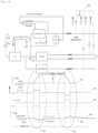
- FIG. 1 A schematic view of such a supply is illustrated in FIG. 1 .
- the primary HVDC output power source 105 typically comprises a variable HVDC power source capable of delivering tens of kilovolts of output voltage. Commonly known as an accelerator, such a power source form the first stage in an electron supply system.
- a terminal 106 of the primary output power source is connected to one or more secondary HVDC output power sources 103,104 such that they are all referenced to a common 'floating' ground.
- these secondary HVDC output power sources may be 'floating' at several tens of kilovolts away from Earth potential on the primary HVDC output power source 105.
- Exemplary floating secondary HVDC output power sources 103,104 may include, for example, a suppressor output 104 (typically rated to -1000 V DC at 20 uA) suitable for controlling the movement of a cloud of electrons (i.e. charged particles) emitted by an electron emitter, and an extractor output 103 (typically rated to 10 kV DC at 400 uA) suitable for controlling the amount and manner in which the electrons are extracted from the electron emitter.
- a low voltage DC output power source for example, a heater output 107 (typically rated to 5 V DC at 3 A) suitable for powering an electron emitter source (i.e. the electron emitter).
- a heater output 107 typically rated to 5 V DC at 3 A
- primary HVDC output power sources 105 i.e. accelerators
- slew rates i.e. rate of change of output voltage
- An inherit limitation of the electrical architecture of such HVDC power supplies is that increasing the slew rate of the accelerator output may generate voltage disturbances on the floating secondary HVDC outputs which may in turn have an undesirable effect of affecting the biasing of the ebeam column and therefore the characteristics defining the resulting device structure.
- FIG. 1 illustrates an electrical architecture of a typical HVDC power supply 100 for use in Electron Beam Inspection (EBI), Scanning Electron Microscope (SEM) and lithography applications.
- EBI Electron Beam Inspection
- SEM Scanning Electron Microscope
- lithography lithography
- the voltage disturbance mechanism will be explained in further detail in the latter sections.
- a capacitive divider is formed between the floating extractor output capacitance (C2) 101 and cable capacitance (C8) 102, which in turn creates an undesirable voltage disturbance on the extractor output.
- the time the extractor output takes to settle is finite and depends on the transient response of the power source.
- the invention seeks to provide for a HVDC power supply and related supply method having advantages over known such supplies and methods.
- the invention seeks to provide for a HVDC power supply and related supply method which can address problems in the current art without exhibiting at least one of the limitations noted above.
- the present invention provides a high voltage direct current power supply according to claim 1.
- the present invention provides a method of providing high voltage direct current power according to claim 15.
- FIG. 2 is an exemplary schematic view of a typical circuit architecture of such a HVDC power supply.
- the circuit shows a primary HVDC output power source (an accelerator) where the output is referenced to Earth potential 202 and two secondary 'floating' HVDC output power sources, an extractor 203 and a suppressor 204.
- the outputs of these secondary sources are both referenced to a 'floating' ground Heater_0V 201, which may be 'floating' at several tens of kilovolts away from Earth potential on the primary HVDC output power source .
- the voltage disturbance mechanism analyses to follow will focus primarily on the extractor source. It will be understood that the same voltage deviation mechanism equally affects the suppressor source.
- a low voltage DC output power source i.e. a heater output 206 also referenced to the 'floating' ground Heate_0V.
- a heater output 206 also referenced to the 'floating' ground Heate_0V.
- the operation of the low voltage DC output power source is not being considered in this application.
- the extractor 203 effectively presents a output having a capacitance Cf 205 which appears as connected in parallel with the extractor output and 'floating' ground Heater_0V is the output filter capacitor Cf of the extractor 205.
- the potential between the extractor output and Heater_0V is denoted by V_Extractor and the potential between the accelerator and 'Earth' ground is denoted by V_acc.
- the output voltage V_acc, of the primary HVDC output power source i.e. the accelerator
- the output voltage V_acc is ramped down at a constant rate from a pre-set magnitude.
- the effects of ramping down V_acc on the output voltage of the extractor V_Extractor is illustrated in FIG. 3 .
- the current in the capacitor Cf flows in a direction into Cf towards Heater_0V as shown in FIG. 3 . This will be referred to hereon in as a 'negative excursion' and is representative of the voltage at the Heater_0V being forced further away from Earth potential.
- Voltage trace 301 in FIG. 3 shows the voltage output waveform V_acc 304 of the accelerator.
- Current trace 302 in FIG. 3 shows the current waveform of the current flowing through the filter capacitor Cf.
- Voltage trace 303 in FIG. 3 shows the voltage output waveform V_Extractor of the extractor.
- the accelerator voltage output V_acc is originally set at a pre-set magnitude of, for example, 100V. During this period of operation with no V_acc voltage change, there is no current flow through the feedback capacitor Cf 305. As V_acc 304 is ramped down at a constant rate, a constant current flows into Cf 305 towards Heater_0V 306 ('floating' ground), as illustrated in the trace 302 in FIG. 3 .
- the voltage output waveform of the extractor V_Extractor is distorted in that it increases at a constant rate as a direct result of the voltage deviation mechanism in operation i.e. the capacitive divider effect described in the background section.
- V_Extractor starts to recover to its original value at a rate which depends on the transient response of the extractor, capacitance values and circuit time constants as shown in 303 in FIG.3 .
- FIG. 4 illustrates a trace of the voltage measured at V_Extractor 401,402 and Heater_0V.
- the voltage differential between V_Extractor and Heater_0V is shown at 404 during the negative excursion.
- Trace 401 shows the extractor voltage with respect to 'Earth' ground, i.e. V_acc + V_Extractor.
- Trace 402, superimposed over 401 is a dotted trace showing the extractor voltage with respect to 'Earth' assuming that Cf is not present or has no effect across the extractor output.
- the resulting voltage disturbance can be in the region of several tens of volts.
- a voltage disturbance of this magnitude may be detrimental to the normal operation of the system powered by the HVDC power supply.
- biasing of an ebeam column could be affected causing delays in operation or under/over emission.
- FIG. 5 illustrates the voltage measured at V_Suppressor 501,502 and at Heater_0V 503 and the voltage differential between V_Suppressor and Heater_0V 504 during the negative current excursion.
- 501 shows the extractor voltage with respect to 'Earth' ground, i.e. V_acc + V_Suppressor. 502, superimposed over 501, is a dotted trace showing the extractor voltage with respect to 'Earth' assuming that Cf is not present across the extractor output.
- Cf capacitive divider effect
- the output voltage V_acc, of the primary HVDC output power source i.e. the accelerator
- the output voltage V_acc of the primary HVDC output power source (i.e. the accelerator) is ramped up at a constant rate from 'Earth' potential to an arbitrary value, for example, 100V.
- the effects of ramping up V_acc on the output voltage of the extractor V_Extractor is illustrated in FIG. 6 .
- the current in the capacitor Cf flows in a direction away from CF and the extractor as shown in FIG. 6 . This will be referred to hereon in as a ⁇ positive current excursion'.
- Voltage trace 601 in FIG. 6 shows the voltage output waveform V_acc 604 of the accelerator.
- Current trace 602 in FIG. 6 shows the current waveform of the current flowing through the filter capacitor Cf 605.
- Voltage trace 603 in FIG. 6 shows the voltage output waveform V_Extractor of the extractor.
- the accelerator voltage output V_acc 604 is originally at 'Earth' potential. During this period of operation, no current flow through the feedback capacitor Cf. As V_acc is ramped up at a constant rate, a constant current starts to flow away from Cf 605 and the extractor as illustrated in the trace 602 in FIG. 6 .
- the voltage output waveform of the extractor V_Extractor is again distorted in that it decreases at a constant rate as a direct result of the voltage deviation mechanism in operation i.e. the capacitive divider effect described in the background section.
- V_Extractor starts to recover to its original value at a rate which depends on the transient response of the extractor, capacitance values and circuit time constants as shown in 603 in FIG. 6 .
- the voltage disturbance mechanism on the 'floating' secondary low voltage DC output power source is negligible as the output capacitance Cf of the heater is very large and the output impedance is low compared to the other outputs
- the disclosure herein is directed towards the provision of a system that is suitable for mitigating the voltage disturbances arising in HVDC systems used for electron emission and in particular for a HVDC power supply for use, for example, in Electron Beam Inspection (EBI), Scanning Electron Microscope (SEM) and lithography applications.
- EBI Electron Beam Inspection
- SEM Scanning Electron Microscope
- the PCS is configured to operate in such a manner that it prevents the extractor output capacitance from being charged up by effectively offering a current sink, thereby controlling at all times the magnitude of V_Extractor, during the periods when the HVDC power supply is undergoing both the positive and negative excursions.
- a programmable current source PCS 701 is connected in parallel with the output of one of the 'floating' secondary HVDC output power sources, for example, between the positive output terminal and the 'floating' ground of the extractor, as illustrated in FIGs.7(a) and 7(b) .
- a PCS is connected in parallel with the output of another one of the 'floating' secondary HVDC output power sources, for example, between the positive output terminal and the 'floating' ground of the suppressor.
- a PCS is connected in parallel with the output of more than one of the 'floating' secondary HVDC output power sources, for example, between the positive output terminal and the 'floating' ground of the suppressor and the extractor.
- the PCS may comprise a chain of MOSFET devices 801 connected in a manner as shown in FIG. 8 , configured to operate as part of a constant current sink that may be regulated using a current controller 804.
- the chain of MOSFET devices 801 within the PCS may be regulated by any other suitable controlling means, for example, using a voltage controller to achieve the desired current sink effect.
- the PCS may also comprise a chain of any other suitable power electronic devices, for example, BJTs, IGBTs or JFETs for the purpose of sinking current.
- the PCS may also comprise an output voltage deviation sensing circuitry 802,803,805 that is configured to monitor the difference between the demanded and measured output voltage of the one or more 'floating' secondary HVDC output power sources.
- the output voltage deviation sensing circuitry generates, for each 'floating' secondary HVDC output power source, a control signal for use by the current controller based on the detected voltage output deviation or error for the respective power sources.
- the current controller may increase or decrease the magnitude of the constant current sink by varying the transconductance of the MOSFET devices in the chain, based on the received control signal, that is, the amount of deviation detected between the demanded and measured output voltage.
- the system may also comprise any other suitable programmable current sources configured such that they may be connected in parallel with the output of one/or more of the 'floating' secondary HVDC output power sources (that is, between the positive output terminal and the 'floating' ground of the suppressor and/or extractor) to achieve the same technical effect of suppressing the aforementioned voltage disturbances.
- the output voltage sensing circuity may comprise a combination of circuits such as a resistive potential divider circuit 805, a buffer circuit 802 and an inverter circuit 803, configured in a manner as shown in FIG. 8 .
- the output voltage sensing circuitry compares the deviation between two input voltages, i.e. the difference between the demanded and measured output voltage of the 'floating' secondary HVDC output power source, to generate in real time the control signal 806 for use by the current controller 804 to regulate the constant current sink in real time.
- the system may comprise any other suitable means for sensing the differential between the demanded and measured output voltages of the 'floating' secondary HVDC output power sources, for example, using a current sensor to measure the current and predicting the expected voltage difference or use a fixed correction value based on changes in demand voltages.
- the system may also comprise any other suitable means for generating the control signal based on the sensed differential, for example, using YYY.
- the current controller 804 may comprise a sense resistor and amplifier configured in a manner as shown in FIG. 8 .
- the current controller varies the transconductance of one or more MOSFETs in the MOSFET chain 801 based on the input control signal 806 supplied by the output voltage sensing circuitry 802,803,805.
- the PCS diverts excess 'parasitic' current generated from the capacitive divider effect, as explained in the preceding section, due to the capacitive divider effect from the output capacitance of the 'floating' secondary HVDC output power source (e.g. the extractor output capacitance) and the cable capacitance. In doing so, unwanted deviations to the output voltage of the 'floating' secondary HVDC output power source when the primary HVDC output power source is ramped up or down can be minimised.
- the output capacitance of the 'floating' secondary HVDC output power source e.g. the extractor output capacitance
- FIG. 7 (a) shows the voltage waveform of V_Extractor 704,705 during both a positive current excursion (i.e. ramping up of V_acc) and a negative current excursion (i.e. ramping down of V_acc), the two operating modes described in the preceding paragraphs.
- Voltage trace 704 in FIG. 7(a) shows the voltage output waveform V_Extractor (no compensation) of the extractor with no PCS compensation.
- the PCS detects deviation between the demanded and measured output voltage of the extractor and reacts by adjusting the magnitude the constant current sink to divert the current away from charging the extractor filter capacitance Cf, thereby controlling V_Extractor.
- the effect of the PCS is shown by the V_Extractor (with PCS compensation) 705.
- the voltage deviation caused by Cf is no longer present and V_Extractor remains substantially constant during the positive current excursion when V_acc is ramped down.
- V_Extractor remains substantially constant during the time period where V_acc is ramped down at a constant rate.
Landscapes
- Engineering & Computer Science (AREA)
- Automation & Control Theory (AREA)
- Physics & Mathematics (AREA)
- Electromagnetism (AREA)
- General Physics & Mathematics (AREA)
- Radar, Positioning & Navigation (AREA)
- Power Engineering (AREA)
- Chemical & Material Sciences (AREA)
- Analytical Chemistry (AREA)
- Electron Sources, Ion Sources (AREA)
- Control Of Voltage And Current In General (AREA)
- Particle Accelerators (AREA)
- Testing Or Measuring Of Semiconductors Or The Like (AREA)
Description
- The present invention relates to a high voltage direct current power supply, and to a related supply method, such as for use in electron-emission systems such as Electron Beam Inspection (EBI), Scanning Electron Microscope (SEM) and lithography applications. In particular, the invention can relate to a high voltage direct current power supply comprising a 'floating' high voltage electrical power output for the emission and manipulation the of a flow of charged particles for the aforementioned applications.
-
EP1862879 is a document that discusses a power supply apparatus that has a series regulator for generating a predetermined power supply voltage from a DC voltage output from the rectifying circuit, and a capacitor bank of rectifying capacitors for stabilizing the power supply voltage, also comprising a charging bypass circuit connected between input and output terminals of the series regulator. The charging bypass circuit is turned on or off by an externally supplied drive signal. When a drop of the power supply voltage is detected, the charging bypass circuit is turned on. - High Voltage Direct Current HVDC power supplies suitable for use in Electron Beam Inspection (EBI), Scanning Electron Microscope (SEM) and lithography applications typically share a common electrical architecture comprising a primary HVDC power output referenced to Earth potential, and feeding one or more secondary HVDC power outputs referenced to a common 'floating' ground (i.e. several tens of kV from Earth potential). A schematic view of such a supply is illustrated in
FIG. 1 . - The primary HVDC
output power source 105 typically comprises a variable HVDC power source capable of delivering tens of kilovolts of output voltage. Commonly known as an accelerator, such a power source form the first stage in an electron supply system. - A
terminal 106 of the primary output power source is connected to one or more secondary HVDC output power sources 103,104 such that they are all referenced to a common 'floating' ground. In operation, these secondary HVDC output power sources may be 'floating' at several tens of kilovolts away from Earth potential on the primary HVDCoutput power source 105. - Exemplary floating secondary HVDC output power sources 103,104 may include, for example, a suppressor output 104 (typically rated to -1000 V DC at 20 uA) suitable for controlling the movement of a cloud of electrons (i.e. charged particles) emitted by an electron emitter, and an extractor output 103 (typically rated to 10 kV DC at 400 uA) suitable for controlling the amount and manner in which the electrons are extracted from the electron emitter. Also present on the secondary supply side is a low voltage DC output power source, for example, a heater output 107 (typically rated to 5 V DC at 3 A) suitable for powering an electron emitter source (i.e. the electron emitter). However, the operation of the low voltage DC output power source is not being considered in this application.
- As structural complexities and aspect ratios of ebeam related formations continue to develop and place ever greater pressure on system operational requirements, for example, as the complexity of modern Integrated Chip IC design continue to rise requiring structures on wafers to be increasingly more intricate and complicated (i.e. higher aspect ratios and smaller structures), primary HVDC output power sources 105 (i.e. accelerators) are being required to operate at increasingly higher slew rates (i.e. rate of change of output voltage) as the electron beam is scanned over the wafer. This enables the required aspect ratios to be achieved on the surface a wafer to create the complex device structures required to produce high performance ICs used in new emerging applications.
- An inherit limitation of the electrical architecture of such HVDC power supplies is that increasing the slew rate of the accelerator output may generate voltage disturbances on the floating secondary HVDC outputs which may in turn have an undesirable effect of affecting the biasing of the ebeam column and therefore the characteristics defining the resulting device structure.
- Limiting the accelerator slew rate to reduce the voltage disturbances is not a practical solution as this increases the wafer fabrication/processing time substantially. The market is driving for faster inspection time and higher emitter life (i.e. through the adoption of smaller column V changes).
-
FIG. 1 illustrates an electrical architecture of a typicalHVDC power supply 100 for use in Electron Beam Inspection (EBI), Scanning Electron Microscope (SEM) and lithography applications. The voltage disturbance mechanism will be explained in further detail in the latter sections. In principle, if the accelerator output voltage is increased or decreased rapidly, a capacitive divider is formed between the floating extractor output capacitance (C2) 101 and cable capacitance (C8) 102, which in turn creates an undesirable voltage disturbance on the extractor output. The time the extractor output takes to settle is finite and depends on the transient response of the power source. - While it may be possible to install capacitors with suitable capacitance to smooth out the voltage disturbances to the floating extractor and suppressor outputs, such an approach is not practical as this creates an energy hazard from unintended rapid discharge of the capacitors and effects the response and settling time of the output.
- The invention seeks to provide for a HVDC power supply and related supply method having advantages over known such supplies and methods. In particular, the invention seeks to provide for a HVDC power supply and related supply method which can address problems in the current art without exhibiting at least one of the limitations noted above.
- Aspects and embodiments of the present invention have been devised with the foregoing in mind.
- Viewed from a first aspect, the present invention provides a high voltage direct current power supply according to
claim 1. - Viewed from a second aspect, the present invention provides a method of providing high voltage direct current power according to claim 15.
- Aspects and advantages of embodiments of the present invention will be more fully understood and appreciated upon consideration of the following detailed description and accompanying drawings, which set forth illustrative embodiments by way of example only.
-
-
Figure 1 is a block diagram view of a HVDC power supply, for example, for use in Electron Beam Inspection (EBI), Scanning Electron Microscope (SEM) and lithography applications; -
Figure 2 is a schematic view illustration of the HVDC power supply including a plot of several voltage traces derived from the circuit; -
Figure 3 is a schematic view illustration of the HVDC power supply including a plot of several voltage traces derived from the circuit during a negative excursion; -
Figure 4 is a plot of the extractor output voltage trace, the 'floating' ground Heater_0V trace and the differential potential between the two during a negative excursion; -
Figure 5 is a plot of the suppressor output voltage trace, the 'floating' ground Heater_0V trace and the differential potential between the two during a negative excursion -
Figure 6 is a schematic view illustration of the HVDC power supply including a plot of several voltage traces derived from the circuit during a positive excursion -
Figure 7(a) is a schematic view illustration of the HVDC power supply connected to a programmable current source PCS including a plot of several voltage traces derived from the circuit during a positive and negative excursion; -
Figure 7(b) is a block diagram view of the PCS; and -
Figure 8 is a schematic view of the circuit layout of the PCS. - Aspects and embodiments of the invention are not limited to the following description, as such may, of course, vary. It is also to be understood that the terminology used herein is for the purpose of describing particular embodiments only, and not intended to be limiting, since the scope of protection sought will be limited only by the appended claims construed or interpreted in accordance with prevailing practice and law.
- Unless defined otherwise, all technical and scientific terms used herein have the same meaning as commonly understood by one of ordinary skill in the art to which aspects and embodiments of this invention belongs or as determined by the context in which they are used. Although any methods and materials similar or equivalent to those described herein can also be used in the practice or testing of the present invention, a limited number of illustrative methods and materials are described herein.
- In order to better illustrate the voltage disturbance mechanism affecting the normal function of the 'floating' secondary HVDC output power source (i.e. an extractor or suppressor), different modes of operation of the HVDC power supply will now be analysed.
-
FIG. 2 is an exemplary schematic view of a typical circuit architecture of such a HVDC power supply. The circuit shows a primary HVDC output power source (an accelerator) where the output is referenced to Earthpotential 202 and two secondary 'floating' HVDC output power sources, anextractor 203 and asuppressor 204. The outputs of these secondary sources are both referenced to a 'floating'ground Heater_0V 201, which may be 'floating' at several tens of kilovolts away from Earth potential on the primary HVDC output power source . The voltage disturbance mechanism analyses to follow will focus primarily on the extractor source. It will be understood that the same voltage deviation mechanism equally affects the suppressor source. Also present on the secondary supply side is a low voltage DC output power source i.e. aheater output 206 also referenced to the 'floating' ground Heate_0V. However, the operation of the low voltage DC output power source is not being considered in this application. - The
extractor 203 effectively presents a output having acapacitance Cf 205 which appears as connected in parallel with the extractor output and 'floating' ground Heater_0V is the output filter capacitor Cf of theextractor 205. The potential between the extractor output and Heater_0V is denoted by V_Extractor and the potential between the accelerator and 'Earth' ground is denoted by V_acc. - In a first operating mode, the output voltage V_acc, of the primary HVDC output power source (i.e. the accelerator) is ramped down at a constant rate from a pre-set magnitude. The effects of ramping down V_acc on the output voltage of the extractor V_Extractor is illustrated in
FIG. 3 . In this operating mode, the current in the capacitor Cf flows in a direction into Cf towards Heater_0V as shown inFIG. 3 . This will be referred to hereon in as a 'negative excursion' and is representative of the voltage at the Heater_0V being forced further away from Earth potential. -
Voltage trace 301 inFIG. 3 shows the voltageoutput waveform V_acc 304 of the accelerator.Current trace 302 inFIG. 3 shows the current waveform of the current flowing through the filter capacitor Cf.Voltage trace 303 inFIG. 3 shows the voltage output waveform V_Extractor of the extractor. The accelerator voltage output V_acc is originally set at a pre-set magnitude of, for example, 100V. During this period of operation with no V_acc voltage change, there is no current flow through thefeedback capacitor Cf 305. AsV_acc 304 is ramped down at a constant rate, a constant current flows intoCf 305 towards Heater_0V 306 ('floating' ground), as illustrated in thetrace 302 inFIG. 3 . During the time period that V_acc is ramping down, the voltage output waveform of the extractor V_Extractor is distorted in that it increases at a constant rate as a direct result of the voltage deviation mechanism in operation i.e. the capacitive divider effect described in the background section. - Once the ramping down of V_acc ceases, the consequent constant current flowing through
Cf 305 ceases as shown intrace 302 inFIG. 3 . V_Extractor starts to recover to its original value at a rate which depends on the transient response of the extractor, capacitance values and circuit time constants as shown in 303 inFIG.3 . - The voltage disturbance on the extractor output during negative excursion can be more clearly observed in
FIG. 4. FIG. 4 illustrates a trace of the voltage measured at V_Extractor 401,402 and Heater_0V. The voltage differential between V_Extractor and Heater_0V is shown at 404 during the negative excursion.Trace 401 shows the extractor voltage with respect to 'Earth' ground, i.e. V_acc + V_Extractor.Trace 402, superimposed over 401, is a dotted trace showing the extractor voltage with respect to 'Earth' assuming that Cf is not present or has no effect across the extractor output. The effect of the voltage disturbance to the extractor voltage with respect to 'Earth' ground due to the capacitive divider effect (Cf) is clear from the overlapping traces of 401 and 402, and a comparison of 401 and 402 confirms the source of theproblematic trace 404, primarily due to the lag at the extractor output. - Taking into consideration the circuit constants, cable capacitance, and typical values of voltage slew rate, the resulting voltage disturbance can be in the region of several tens of volts. A voltage disturbance of this magnitude may be detrimental to the normal operation of the system powered by the HVDC power supply. For example, biasing of an ebeam column could be affected causing delays in operation or under/over emission.
- The voltage disturbance on the suppressor output during negative current excursion is also provided in
FIG. 5 for completeness.FIG. 5 illustrates the voltage measured at V_Suppressor 501,502 and atHeater_0V 503 and the voltage differential between V_Suppressor andHeater_0V 504 during the negative current excursion. 501 shows the extractor voltage with respect to 'Earth' ground, i.e. V_acc + V_Suppressor. 502, superimposed over 501, is a dotted trace showing the extractor voltage with respect to 'Earth' assuming that Cf is not present across the extractor output. The effect of the voltage disturbance to the extractor voltage with respect to 'Earth' ground due to the capacitive divider effect (Cf) is clear from the overlapping traces of 501 and 502. - In a second operating mode, the output voltage V_acc, of the primary HVDC output power source (i.e. the accelerator) is ramped up at a constant rate from 'Earth' potential to an arbitrary value, for example, 100V. The effects of ramping up V_acc on the output voltage of the extractor V_Extractor is illustrated in
FIG. 6 . In this operating mode, the current in the capacitor Cf flows in a direction away from CF and the extractor as shown inFIG. 6 . This will be referred to hereon in as a `positive current excursion'. -
Voltage trace 601 inFIG. 6 shows the voltageoutput waveform V_acc 604 of the accelerator.Current trace 602 inFIG. 6 shows the current waveform of the current flowing through thefilter capacitor Cf 605.Voltage trace 603 inFIG. 6 shows the voltage output waveform V_Extractor of the extractor. The acceleratorvoltage output V_acc 604 is originally at 'Earth' potential. During this period of operation, no current flow through the feedback capacitor Cf. As V_acc is ramped up at a constant rate, a constant current starts to flow away fromCf 605 and the extractor as illustrated in thetrace 602 inFIG. 6 . During the time period thatV_acc 604 is ramping up, the voltage output waveform of the extractor V_Extractor is again distorted in that it decreases at a constant rate as a direct result of the voltage deviation mechanism in operation i.e. the capacitive divider effect described in the background section. - Once the ramping up of V_acc ceases, the consequent constant current flowing through
Cf 605 ceases as shown intrace 602 inFIG. 6 . V_Extractor starts to recover to its original value at a rate which depends on the transient response of the extractor, capacitance values and circuit time constants as shown in 603 inFIG. 6 . - The voltage disturbance mechanism on the 'floating' secondary low voltage DC output power source is negligible as the output capacitance Cf of the heater is very large and the output impedance is low compared to the other outputs
- The disclosure herein is directed towards the provision of a system that is suitable for mitigating the voltage disturbances arising in HVDC systems used for electron emission and in particular for a HVDC power supply for use, for example, in Electron Beam Inspection (EBI), Scanning Electron Microscope (SEM) and lithography applications.
- The PCS is configured to operate in such a manner that it prevents the extractor output capacitance from being charged up by effectively offering a current sink, thereby controlling at all times the magnitude of V_Extractor, during the periods when the HVDC power supply is undergoing both the positive and negative excursions.
- In one arrangement, a programmable
current source PCS 701 is connected in parallel with the output of one of the 'floating' secondary HVDC output power sources, for example, between the positive output terminal and the 'floating' ground of the extractor, as illustrated inFIGs.7(a) and7(b) . In another arrangement, a PCS is connected in parallel with the output of another one of the 'floating' secondary HVDC output power sources, for example, between the positive output terminal and the 'floating' ground of the suppressor. In yet another arrangement, a PCS is connected in parallel with the output of more than one of the 'floating' secondary HVDC output power sources, for example, between the positive output terminal and the 'floating' ground of the suppressor and the extractor. - In one arrangement, the PCS may comprise a chain of
MOSFET devices 801 connected in a manner as shown inFIG. 8 , configured to operate as part of a constant current sink that may be regulated using acurrent controller 804. The chain ofMOSFET devices 801 within the PCS may be regulated by any other suitable controlling means, for example, using a voltage controller to achieve the desired current sink effect. The PCS may also comprise a chain of any other suitable power electronic devices, for example, BJTs, IGBTs or JFETs for the purpose of sinking current. The PCS may also comprise an output voltage deviation sensing circuitry 802,803,805 that is configured to monitor the difference between the demanded and measured output voltage of the one or more 'floating' secondary HVDC output power sources. The output voltage deviation sensing circuitry generates, for each 'floating' secondary HVDC output power source, a control signal for use by the current controller based on the detected voltage output deviation or error for the respective power sources. The current controller may increase or decrease the magnitude of the constant current sink by varying the transconductance of the MOSFET devices in the chain, based on the received control signal, that is, the amount of deviation detected between the demanded and measured output voltage. The system may also comprise any other suitable programmable current sources configured such that they may be connected in parallel with the output of one/or more of the 'floating' secondary HVDC output power sources (that is, between the positive output terminal and the 'floating' ground of the suppressor and/or extractor) to achieve the same technical effect of suppressing the aforementioned voltage disturbances. - In one arrangement, the output voltage sensing circuity may comprise a combination of circuits such as a resistive
potential divider circuit 805, abuffer circuit 802 and aninverter circuit 803, configured in a manner as shown inFIG. 8 . The output voltage sensing circuitry compares the deviation between two input voltages, i.e. the difference between the demanded and measured output voltage of the 'floating' secondary HVDC output power source, to generate in real time thecontrol signal 806 for use by thecurrent controller 804 to regulate the constant current sink in real time. - The system may comprise any other suitable means for sensing the differential between the demanded and measured output voltages of the 'floating' secondary HVDC output power sources, for example, using a current sensor to measure the current and predicting the expected voltage difference or use a fixed correction value based on changes in demand voltages.
- The system may also comprise any other suitable means for generating the control signal based on the sensed differential, for example, using YYY.
- In one arrangement, the
current controller 804 may comprise a sense resistor and amplifier configured in a manner as shown inFIG. 8 . The current controller varies the transconductance of one or more MOSFETs in theMOSFET chain 801 based on theinput control signal 806 supplied by the output voltage sensing circuitry 802,803,805. As the MOSFETs are adjusted, the PCS diverts excess 'parasitic' current generated from the capacitive divider effect, as explained in the preceding section, due to the capacitive divider effect from the output capacitance of the 'floating' secondary HVDC output power source (e.g. the extractor output capacitance) and the cable capacitance. In doing so, unwanted deviations to the output voltage of the 'floating' secondary HVDC output power source when the primary HVDC output power source is ramped up or down can be minimised. - To better illustrate the effect of the proposed system on the output voltage of the extractor,
FIG. 7 (a) shows the voltage waveform of V_Extractor 704,705 during both a positive current excursion (i.e. ramping up of V_acc) and a negative current excursion (i.e. ramping down of V_acc), the two operating modes described in the preceding paragraphs. -
Voltage trace 704 inFIG. 7(a) shows the voltage output waveform V_Extractor (no compensation) of the extractor with no PCS compensation.Voltage trace 705 inFIG.7(a) in dotted line, which is superimposed over 704, shows the voltage output waveform V_Extractor (with PCS compensation). - During the positive current excursion, i.e. the
region 706, as V_acc is ramped up, the PCS detects deviation between the demanded and measured output voltage of the extractor and reacts by adjusting the magnitude the constant current sink to divert the current away from charging the extractor filter capacitance Cf, thereby controlling V_Extractor. The effect of the PCS is shown by the V_Extractor (with PCS compensation) 705. The voltage deviation caused by Cf is no longer present and V_Extractor remains substantially constant during the positive current excursion when V_acc is ramped down. - A similar effect is achieved during the negative current excursion as shown in the
region 707. Again, V_Extractor remains substantially constant during the time period where V_acc is ramped down at a constant rate. - Particular and preferred aspects of the invention are set out in the accompanying independent claims. Combinations of features from the dependent and/or independent claims may be combined as appropriate and as set out in the claims.
- Term "comprising" does not exclude other elements or steps, the term "a" or "an" does not exclude a plurality. Reference signs in the claims shall not be construed as limiting the scope of the claims.
Claims (16)
- A high voltage direct current power supply (100) comprising:a primary high voltage direct current supply (105) offering a primary output (106);a floating secondary power supply (103, 104, 107, 203, 204) floating with respect to the primary output (106) and connected to the primary output (106); andan output terminal (800) at the floating secondary power supply for providing an output voltage; characterised in that the high voltage direct current power supply further comprises:a controller (701, 802, 803, 804, 805) operative to detect a change in the output voltage at the output terminal (800) and to generate a control signal (806) responsive to the change in output voltage; anda controllable current source (801, 804) arranged to provide current at the floating secondary power supply (103, 104, 107, 203, 204) responsive to the said control signal (806) and whereby the said current is provided to reduce charging of a secondary output capacitance (205, 305) as the output voltage changes, wherein the secondary output capacitance corresponds to an output capacitance of the floating secondary power supply; and wherein the controllable current source comprises:a chain of power electronic devices (801) configured to operate as a constant current sink; and whereinthe controllable current source increases or decreases a magnitude of the constant current sink by varying a transconductance of the power electronic devices in the chain based on the control signal.
- A power supply as claimed in claim 1, wherein the controllable current source (801, 804) is arranged in parallel with the floating secondary power supply (103, 104, 107, 203, 204).
- A power supply as claimed in claim 1 or 2, wherein the controllable current source (801, 804) comprises a programmable current source.
- A power supply as claimed in any one or more of the preceding claims and arranged to be regulated by way of a sense resistor.
- A power supply as claimed in any one or more of the preceding claims, wherein the controller (701, 802, 803, 804, 805) includes a resistor divider for detecting changes in the output voltage at the output terminal.
- A power supply as claimed in any one or more preceding claims wherein the controller (701, 802, 803, 804, 805) is arranged to produce an error signal for regulating the current source.
- A power supply as claimed in claim 6 wherein the controller (701, 802, 803, 804, 805) is arranged to regulate a transistor chain of the current source, the transistor chain comprising the chain of power electronic devices and operating as the constant current sink.
- A power supply as claimed in any one or more of the preceding claims, wherein the primary high voltage direct current supply is an accelerator power supply (105).
- The high voltage current power supply of any one or more of the preceding claims, wherein the floating secondary power supply is a suppressor (104).
- The high voltage direct current power supply of claim 9, wherein the suppressor has a rated output voltage within a range of -100 V to -3kV.
- The high voltage direct current power supply of claims 9, wherein the suppressor has a rated output power within a range of 0.1W to 50W.
- The high voltage direct current power supply of any one or more of the preceding claims, wherein the floating power supply is an extractor (103).
- The high voltage direct current power supply of claim 12, wherein the extractor has a rated output voltage within a range of 1kV to 15kV.
- The high voltage direct current power supply of claim 12, wherein the extractor has a rated output power within a range of 0.1W to 20W.
- A method of providing high voltage direct current power comprising:providing a primary output (106) at a primary high voltage direct current supply (105);providing a floating secondary power supply (103, 104, 107, 203, 204) floating with respect to the primary output (106) and connecting the floating secondary power supply to the primary output (106): andproviding an output voltage at an output terminal (800) of the floating secondary power supply; the method characterised in that it further comprises:
detecting a change in the output voltage at the output terminal (800) and generating a control signal (806) responsive to the change in output voltage; andproviding, by way of a controllable current source (801, 804), current at the floating secondary power supply (103, 104, 107, 203, 204) responsive to the said control signal (806) and whereby the said current is provided to reduce charging of a secondary output capacitance (205, 305) as the output voltage changes, wherein the secondary output capacitance corresponds to an output capacitance of the floating secondary power supply, and wherein the controllable current source comprises:a chain of power electronic devices (801) configured to operate as a constant current sink; and whereinthe controllable current source increases or decreases a magnitude of the constant current sink by varying a transconductance of the power electronic devices in the chain based on the control signal. - The method of claim 15, and providing the high voltage direct current power by way of a power supply according to any one or more of claims 2-14.
Priority Applications (5)
| Application Number | Priority Date | Filing Date | Title |
|---|---|---|---|
| EP19184399.4A EP3761148B1 (en) | 2019-07-04 | 2019-07-04 | High voltage power supply |
| IL289587A IL289587B2 (en) | 2019-07-04 | 2020-07-03 | High voltage power supply |
| JP2021578025A JP2022539213A (en) | 2019-07-04 | 2020-07-03 | high voltage power supply |
| US17/623,687 US11764033B2 (en) | 2019-07-04 | 2020-07-03 | High voltage power supply |
| PCT/US2020/040803 WO2021003458A1 (en) | 2019-07-04 | 2020-07-03 | High voltage power supply |
Applications Claiming Priority (1)
| Application Number | Priority Date | Filing Date | Title |
|---|---|---|---|
| EP19184399.4A EP3761148B1 (en) | 2019-07-04 | 2019-07-04 | High voltage power supply |
Publications (2)
| Publication Number | Publication Date |
|---|---|
| EP3761148A1 EP3761148A1 (en) | 2021-01-06 |
| EP3761148B1 true EP3761148B1 (en) | 2023-06-07 |
Family
ID=67180638
Family Applications (1)
| Application Number | Title | Priority Date | Filing Date |
|---|---|---|---|
| EP19184399.4A Active EP3761148B1 (en) | 2019-07-04 | 2019-07-04 | High voltage power supply |
Country Status (5)
| Country | Link |
|---|---|
| US (1) | US11764033B2 (en) |
| EP (1) | EP3761148B1 (en) |
| JP (1) | JP2022539213A (en) |
| IL (1) | IL289587B2 (en) |
| WO (1) | WO2021003458A1 (en) |
Families Citing this family (1)
| Publication number | Priority date | Publication date | Assignee | Title |
|---|---|---|---|---|
| US12609271B2 (en) * | 2023-10-17 | 2026-04-21 | Advanced Energy Industries, Inc. | High voltage power supplies for fast voltage changes |
Family Cites Families (11)
| Publication number | Priority date | Publication date | Assignee | Title |
|---|---|---|---|---|
| US4400660A (en) * | 1981-09-23 | 1983-08-23 | Sperry Corporation | Wide bandwidth high voltage regulator and modulator |
| TW548679B (en) * | 1998-12-16 | 2003-08-21 | Advantest Corp | Generation apparatus of charged particles |
| JP5255189B2 (en) * | 2006-05-31 | 2013-08-07 | 株式会社ネットコムセック | Power supply device and high-frequency circuit system |
| WO2013127463A1 (en) | 2012-03-01 | 2013-09-06 | Alstom Technology Ltd | High voltage dc circuit breaker apparatus |
| JP2013196324A (en) | 2012-03-19 | 2013-09-30 | Advantest Corp | Power supply device, test device using the same and control method for power supply voltage |
| EP2750271A1 (en) * | 2012-12-28 | 2014-07-02 | Alstom Technology Ltd | Control circuit |
| CN105934818B (en) | 2014-01-21 | 2019-03-29 | 英飞凌科技奥地利有限公司 | Integrated high-side gate driver structure and circuit for driving high-side power transistors |
| US10069296B2 (en) * | 2014-02-05 | 2018-09-04 | Marotta Controls, Inc. | PCU PPFC surge limiter |
| WO2016000774A1 (en) * | 2014-07-03 | 2016-01-07 | Abb Technology Ltd | Inrush current limitation during system energizing |
| CN105356438B (en) * | 2015-11-25 | 2019-03-05 | 珠海万力达电气自动化有限公司 | A DC high voltage overvoltage protection circuit |
| WO2019016857A1 (en) * | 2017-07-18 | 2019-01-24 | 株式会社日立ハイテクノロジーズ | Charged particle beam device |
-
2019
- 2019-07-04 EP EP19184399.4A patent/EP3761148B1/en active Active
-
2020
- 2020-07-03 WO PCT/US2020/040803 patent/WO2021003458A1/en not_active Ceased
- 2020-07-03 US US17/623,687 patent/US11764033B2/en active Active
- 2020-07-03 JP JP2021578025A patent/JP2022539213A/en active Pending
- 2020-07-03 IL IL289587A patent/IL289587B2/en unknown
Also Published As
| Publication number | Publication date |
|---|---|
| IL289587A (en) | 2022-03-01 |
| US11764033B2 (en) | 2023-09-19 |
| IL289587B1 (en) | 2024-10-01 |
| JP2022539213A (en) | 2022-09-07 |
| IL289587B2 (en) | 2025-02-01 |
| EP3761148A1 (en) | 2021-01-06 |
| WO2021003458A1 (en) | 2021-01-07 |
| US20220246390A1 (en) | 2022-08-04 |
Similar Documents
| Publication | Publication Date | Title |
|---|---|---|
| US9977443B2 (en) | Low dropout linear regulators and starting methods therefor | |
| CN106569535B (en) | Voltage regulator with dropout detector and bias current limiter and related method | |
| CN102854908B (en) | Regulator SIC (semiconductor integrated circuit) | |
| JP5291636B2 (en) | Power supply circuit and test equipment | |
| CN112019012B (en) | power circuit | |
| US10756621B2 (en) | Voltage regulators with controlled output voltage and the method thereof | |
| CN108255228B (en) | Circuit for reducing negative pulse signal at output end in voltage stabilizer and method of voltage stabilization | |
| CN104699153B (en) | Low-dropout linear regulator | |
| US8022684B2 (en) | External regulator reference voltage generator circuit | |
| CN107508462B (en) | Load-specific switching controller and method | |
| TWI516895B (en) | Low-drop regulator apparatus and buffer stage circuit | |
| US11165337B2 (en) | Integrated circuit for power factor correction and power supply circuit containing the same | |
| EP3761148B1 (en) | High voltage power supply | |
| TW201833707A (en) | Voltage generator | |
| KR20080090818A (en) | Power factor correction circuit | |
| EP2658107B1 (en) | Power-factor correction using voltage-to-current matching | |
| CN110828265B (en) | Power supply circuit and field emission electron source | |
| US12313696B2 (en) | Test load circuit | |
| US10476610B2 (en) | Semiconductor integrated circuit, semiconductor system, and electric source voltage control method | |
| CN101853039B (en) | Reference voltage supply circuit and supply method thereof, voltage adjustment circuit | |
| KR102710852B1 (en) | Apparatus for detecting current | |
| CN113497558B (en) | Voltage stabilization control system and method thereof | |
| CN105700612B (en) | Voltage regulator | |
| JP2008011585A (en) | Switching regulator | |
| CN113156212B (en) | DC offset output system and method of AC self-balancing bridge |
Legal Events
| Date | Code | Title | Description |
|---|---|---|---|
| PUAI | Public reference made under article 153(3) epc to a published international application that has entered the european phase |
Free format text: ORIGINAL CODE: 0009012 |
|
| STAA | Information on the status of an ep patent application or granted ep patent |
Free format text: STATUS: THE APPLICATION HAS BEEN PUBLISHED |
|
| AK | Designated contracting states |
Kind code of ref document: A1 Designated state(s): AL AT BE BG CH CY CZ DE DK EE ES FI FR GB GR HR HU IE IS IT LI LT LU LV MC MK MT NL NO PL PT RO RS SE SI SK SM TR |
|
| AX | Request for extension of the european patent |
Extension state: BA ME |
|
| STAA | Information on the status of an ep patent application or granted ep patent |
Free format text: STATUS: REQUEST FOR EXAMINATION WAS MADE |
|
| 17P | Request for examination filed |
Effective date: 20210705 |
|
| RBV | Designated contracting states (corrected) |
Designated state(s): AL AT BE BG CH CY CZ DE DK EE ES FI FR GB GR HR HU IE IS IT LI LT LU LV MC MK MT NL NO PL PT RO RS SE SI SK SM TR |
|
| GRAP | Despatch of communication of intention to grant a patent |
Free format text: ORIGINAL CODE: EPIDOSNIGR1 |
|
| STAA | Information on the status of an ep patent application or granted ep patent |
Free format text: STATUS: GRANT OF PATENT IS INTENDED |
|
| RIC1 | Information provided on ipc code assigned before grant |
Ipc: G05F 1/56 20060101ALN20220622BHEP Ipc: H02H 9/04 20060101ALI20220622BHEP Ipc: H01J 37/24 20060101ALI20220622BHEP Ipc: G05F 1/613 20060101AFI20220622BHEP |
|
| INTG | Intention to grant announced |
Effective date: 20220719 |
|
| GRAJ | Information related to disapproval of communication of intention to grant by the applicant or resumption of examination proceedings by the epo deleted |
Free format text: ORIGINAL CODE: EPIDOSDIGR1 |
|
| STAA | Information on the status of an ep patent application or granted ep patent |
Free format text: STATUS: REQUEST FOR EXAMINATION WAS MADE |
|
| GRAP | Despatch of communication of intention to grant a patent |
Free format text: ORIGINAL CODE: EPIDOSNIGR1 |
|
| STAA | Information on the status of an ep patent application or granted ep patent |
Free format text: STATUS: GRANT OF PATENT IS INTENDED |
|
| INTC | Intention to grant announced (deleted) | ||
| RIC1 | Information provided on ipc code assigned before grant |
Ipc: G05F 1/56 20060101ALN20221122BHEP Ipc: H02H 9/04 20060101ALI20221122BHEP Ipc: H01J 37/24 20060101ALI20221122BHEP Ipc: G05F 1/613 20060101AFI20221122BHEP |
|
| INTG | Intention to grant announced |
Effective date: 20221221 |
|
| GRAS | Grant fee paid |
Free format text: ORIGINAL CODE: EPIDOSNIGR3 |
|
| GRAA | (expected) grant |
Free format text: ORIGINAL CODE: 0009210 |
|
| STAA | Information on the status of an ep patent application or granted ep patent |
Free format text: STATUS: THE PATENT HAS BEEN GRANTED |
|
| AK | Designated contracting states |
Kind code of ref document: B1 Designated state(s): AL AT BE BG CH CY CZ DE DK EE ES FI FR GB GR HR HU IE IS IT LI LT LU LV MC MK MT NL NO PL PT RO RS SE SI SK SM TR |
|
| REG | Reference to a national code |
Ref country code: GB Ref legal event code: FG4D |
|
| REG | Reference to a national code |
Ref country code: CH Ref legal event code: EP Ref country code: AT Ref legal event code: REF Ref document number: 1576997 Country of ref document: AT Kind code of ref document: T Effective date: 20230615 |
|
| REG | Reference to a national code |
Ref country code: DE Ref legal event code: R096 Ref document number: 602019029804 Country of ref document: DE |
|
| REG | Reference to a national code |
Ref country code: LT Ref legal event code: MG9D |
|
| REG | Reference to a national code |
Ref country code: NL Ref legal event code: MP Effective date: 20230607 |
|
| P01 | Opt-out of the competence of the unified patent court (upc) registered |
Effective date: 20230908 |
|
| PG25 | Lapsed in a contracting state [announced via postgrant information from national office to epo] |
Ref country code: SE Free format text: LAPSE BECAUSE OF FAILURE TO SUBMIT A TRANSLATION OF THE DESCRIPTION OR TO PAY THE FEE WITHIN THE PRESCRIBED TIME-LIMIT Effective date: 20230607 Ref country code: NO Free format text: LAPSE BECAUSE OF FAILURE TO SUBMIT A TRANSLATION OF THE DESCRIPTION OR TO PAY THE FEE WITHIN THE PRESCRIBED TIME-LIMIT Effective date: 20230907 Ref country code: ES Free format text: LAPSE BECAUSE OF FAILURE TO SUBMIT A TRANSLATION OF THE DESCRIPTION OR TO PAY THE FEE WITHIN THE PRESCRIBED TIME-LIMIT Effective date: 20230607 |
|
| REG | Reference to a national code |
Ref country code: AT Ref legal event code: MK05 Ref document number: 1576997 Country of ref document: AT Kind code of ref document: T Effective date: 20230607 |
|
| PG25 | Lapsed in a contracting state [announced via postgrant information from national office to epo] |
Ref country code: RS Free format text: LAPSE BECAUSE OF FAILURE TO SUBMIT A TRANSLATION OF THE DESCRIPTION OR TO PAY THE FEE WITHIN THE PRESCRIBED TIME-LIMIT Effective date: 20230607 Ref country code: NL Free format text: LAPSE BECAUSE OF FAILURE TO SUBMIT A TRANSLATION OF THE DESCRIPTION OR TO PAY THE FEE WITHIN THE PRESCRIBED TIME-LIMIT Effective date: 20230607 Ref country code: LV Free format text: LAPSE BECAUSE OF FAILURE TO SUBMIT A TRANSLATION OF THE DESCRIPTION OR TO PAY THE FEE WITHIN THE PRESCRIBED TIME-LIMIT Effective date: 20230607 Ref country code: LT Free format text: LAPSE BECAUSE OF FAILURE TO SUBMIT A TRANSLATION OF THE DESCRIPTION OR TO PAY THE FEE WITHIN THE PRESCRIBED TIME-LIMIT Effective date: 20230607 Ref country code: HR Free format text: LAPSE BECAUSE OF FAILURE TO SUBMIT A TRANSLATION OF THE DESCRIPTION OR TO PAY THE FEE WITHIN THE PRESCRIBED TIME-LIMIT Effective date: 20230607 Ref country code: GR Free format text: LAPSE BECAUSE OF FAILURE TO SUBMIT A TRANSLATION OF THE DESCRIPTION OR TO PAY THE FEE WITHIN THE PRESCRIBED TIME-LIMIT Effective date: 20230908 |
|
| PG25 | Lapsed in a contracting state [announced via postgrant information from national office to epo] |
Ref country code: FI Free format text: LAPSE BECAUSE OF FAILURE TO SUBMIT A TRANSLATION OF THE DESCRIPTION OR TO PAY THE FEE WITHIN THE PRESCRIBED TIME-LIMIT Effective date: 20230607 |
|
| PG25 | Lapsed in a contracting state [announced via postgrant information from national office to epo] |
Ref country code: SK Free format text: LAPSE BECAUSE OF FAILURE TO SUBMIT A TRANSLATION OF THE DESCRIPTION OR TO PAY THE FEE WITHIN THE PRESCRIBED TIME-LIMIT Effective date: 20230607 |
|
| PG25 | Lapsed in a contracting state [announced via postgrant information from national office to epo] |
Ref country code: IS Free format text: LAPSE BECAUSE OF FAILURE TO SUBMIT A TRANSLATION OF THE DESCRIPTION OR TO PAY THE FEE WITHIN THE PRESCRIBED TIME-LIMIT Effective date: 20231007 |
|
| PG25 | Lapsed in a contracting state [announced via postgrant information from national office to epo] |
Ref country code: SM Free format text: LAPSE BECAUSE OF FAILURE TO SUBMIT A TRANSLATION OF THE DESCRIPTION OR TO PAY THE FEE WITHIN THE PRESCRIBED TIME-LIMIT Effective date: 20230607 Ref country code: SK Free format text: LAPSE BECAUSE OF FAILURE TO SUBMIT A TRANSLATION OF THE DESCRIPTION OR TO PAY THE FEE WITHIN THE PRESCRIBED TIME-LIMIT Effective date: 20230607 Ref country code: RO Free format text: LAPSE BECAUSE OF FAILURE TO SUBMIT A TRANSLATION OF THE DESCRIPTION OR TO PAY THE FEE WITHIN THE PRESCRIBED TIME-LIMIT Effective date: 20230607 Ref country code: PT Free format text: LAPSE BECAUSE OF FAILURE TO SUBMIT A TRANSLATION OF THE DESCRIPTION OR TO PAY THE FEE WITHIN THE PRESCRIBED TIME-LIMIT Effective date: 20231009 Ref country code: IS Free format text: LAPSE BECAUSE OF FAILURE TO SUBMIT A TRANSLATION OF THE DESCRIPTION OR TO PAY THE FEE WITHIN THE PRESCRIBED TIME-LIMIT Effective date: 20231007 Ref country code: EE Free format text: LAPSE BECAUSE OF FAILURE TO SUBMIT A TRANSLATION OF THE DESCRIPTION OR TO PAY THE FEE WITHIN THE PRESCRIBED TIME-LIMIT Effective date: 20230607 Ref country code: CZ Free format text: LAPSE BECAUSE OF FAILURE TO SUBMIT A TRANSLATION OF THE DESCRIPTION OR TO PAY THE FEE WITHIN THE PRESCRIBED TIME-LIMIT Effective date: 20230607 Ref country code: AT Free format text: LAPSE BECAUSE OF FAILURE TO SUBMIT A TRANSLATION OF THE DESCRIPTION OR TO PAY THE FEE WITHIN THE PRESCRIBED TIME-LIMIT Effective date: 20230607 |
|
| PG25 | Lapsed in a contracting state [announced via postgrant information from national office to epo] |
Ref country code: PL Free format text: LAPSE BECAUSE OF FAILURE TO SUBMIT A TRANSLATION OF THE DESCRIPTION OR TO PAY THE FEE WITHIN THE PRESCRIBED TIME-LIMIT Effective date: 20230607 |
|
| REG | Reference to a national code |
Ref country code: CH Ref legal event code: PL |
|
| REG | Reference to a national code |
Ref country code: DE Ref legal event code: R097 Ref document number: 602019029804 Country of ref document: DE |
|
| PG25 | Lapsed in a contracting state [announced via postgrant information from national office to epo] |
Ref country code: MC Free format text: LAPSE BECAUSE OF FAILURE TO SUBMIT A TRANSLATION OF THE DESCRIPTION OR TO PAY THE FEE WITHIN THE PRESCRIBED TIME-LIMIT Effective date: 20230607 |
|
| REG | Reference to a national code |
Ref country code: BE Ref legal event code: MM Effective date: 20230731 |
|
| PG25 | Lapsed in a contracting state [announced via postgrant information from national office to epo] |
Ref country code: LU Free format text: LAPSE BECAUSE OF NON-PAYMENT OF DUE FEES Effective date: 20230704 |
|
| PG25 | Lapsed in a contracting state [announced via postgrant information from national office to epo] |
Ref country code: MC Free format text: LAPSE BECAUSE OF FAILURE TO SUBMIT A TRANSLATION OF THE DESCRIPTION OR TO PAY THE FEE WITHIN THE PRESCRIBED TIME-LIMIT Effective date: 20230607 Ref country code: LU Free format text: LAPSE BECAUSE OF NON-PAYMENT OF DUE FEES Effective date: 20230704 |
|
| PLBE | No opposition filed within time limit |
Free format text: ORIGINAL CODE: 0009261 |
|
| STAA | Information on the status of an ep patent application or granted ep patent |
Free format text: STATUS: NO OPPOSITION FILED WITHIN TIME LIMIT |
|
| REG | Reference to a national code |
Ref country code: IE Ref legal event code: MM4A |
|
| PG25 | Lapsed in a contracting state [announced via postgrant information from national office to epo] |
Ref country code: DK Free format text: LAPSE BECAUSE OF FAILURE TO SUBMIT A TRANSLATION OF THE DESCRIPTION OR TO PAY THE FEE WITHIN THE PRESCRIBED TIME-LIMIT Effective date: 20230607 Ref country code: CH Free format text: LAPSE BECAUSE OF NON-PAYMENT OF DUE FEES Effective date: 20230731 |
|
| PG25 | Lapsed in a contracting state [announced via postgrant information from national office to epo] |
Ref country code: SI Free format text: LAPSE BECAUSE OF FAILURE TO SUBMIT A TRANSLATION OF THE DESCRIPTION OR TO PAY THE FEE WITHIN THE PRESCRIBED TIME-LIMIT Effective date: 20230607 |
|
| 26N | No opposition filed |
Effective date: 20240308 |
|
| PG25 | Lapsed in a contracting state [announced via postgrant information from national office to epo] |
Ref country code: SI Free format text: LAPSE BECAUSE OF FAILURE TO SUBMIT A TRANSLATION OF THE DESCRIPTION OR TO PAY THE FEE WITHIN THE PRESCRIBED TIME-LIMIT Effective date: 20230607 Ref country code: IT Free format text: LAPSE BECAUSE OF FAILURE TO SUBMIT A TRANSLATION OF THE DESCRIPTION OR TO PAY THE FEE WITHIN THE PRESCRIBED TIME-LIMIT Effective date: 20230607 Ref country code: BE Free format text: LAPSE BECAUSE OF NON-PAYMENT OF DUE FEES Effective date: 20230731 |
|
| PG25 | Lapsed in a contracting state [announced via postgrant information from national office to epo] |
Ref country code: IE Free format text: LAPSE BECAUSE OF NON-PAYMENT OF DUE FEES Effective date: 20230704 |
|
| PG25 | Lapsed in a contracting state [announced via postgrant information from national office to epo] |
Ref country code: IE Free format text: LAPSE BECAUSE OF NON-PAYMENT OF DUE FEES Effective date: 20230704 |
|
| PG25 | Lapsed in a contracting state [announced via postgrant information from national office to epo] |
Ref country code: BG Free format text: LAPSE BECAUSE OF FAILURE TO SUBMIT A TRANSLATION OF THE DESCRIPTION OR TO PAY THE FEE WITHIN THE PRESCRIBED TIME-LIMIT Effective date: 20230607 |
|
| PG25 | Lapsed in a contracting state [announced via postgrant information from national office to epo] |
Ref country code: BG Free format text: LAPSE BECAUSE OF FAILURE TO SUBMIT A TRANSLATION OF THE DESCRIPTION OR TO PAY THE FEE WITHIN THE PRESCRIBED TIME-LIMIT Effective date: 20230607 |
|
| PGFP | Annual fee paid to national office [announced via postgrant information from national office to epo] |
Ref country code: GB Payment date: 20250529 Year of fee payment: 7 |
|
| PGFP | Annual fee paid to national office [announced via postgrant information from national office to epo] |
Ref country code: FR Payment date: 20250610 Year of fee payment: 7 |
|
| PG25 | Lapsed in a contracting state [announced via postgrant information from national office to epo] |
Ref country code: CY Free format text: LAPSE BECAUSE OF FAILURE TO SUBMIT A TRANSLATION OF THE DESCRIPTION OR TO PAY THE FEE WITHIN THE PRESCRIBED TIME-LIMIT; INVALID AB INITIO Effective date: 20190704 |
|
| PG25 | Lapsed in a contracting state [announced via postgrant information from national office to epo] |
Ref country code: HU Free format text: LAPSE BECAUSE OF FAILURE TO SUBMIT A TRANSLATION OF THE DESCRIPTION OR TO PAY THE FEE WITHIN THE PRESCRIBED TIME-LIMIT; INVALID AB INITIO Effective date: 20190704 |
|
| PGFP | Annual fee paid to national office [announced via postgrant information from national office to epo] |
Ref country code: DE Payment date: 20250604 Year of fee payment: 7 |
|
| PG25 | Lapsed in a contracting state [announced via postgrant information from national office to epo] |
Ref country code: TR Free format text: LAPSE BECAUSE OF FAILURE TO SUBMIT A TRANSLATION OF THE DESCRIPTION OR TO PAY THE FEE WITHIN THE PRESCRIBED TIME-LIMIT Effective date: 20230607 |