EP3758225A1 - Switching circuit and variable attenuator - Google Patents
Switching circuit and variable attenuator Download PDFInfo
- Publication number
- EP3758225A1 EP3758225A1 EP18912940.6A EP18912940A EP3758225A1 EP 3758225 A1 EP3758225 A1 EP 3758225A1 EP 18912940 A EP18912940 A EP 18912940A EP 3758225 A1 EP3758225 A1 EP 3758225A1
- Authority
- EP
- European Patent Office
- Prior art keywords
- switch
- state
- resistor
- switching circuit
- variable attenuator
- Prior art date
- Legal status (The legal status is an assumption and is not a legal conclusion. Google has not performed a legal analysis and makes no representation as to the accuracy of the status listed.)
- Granted
Links
Images

Classifications
-
- H—ELECTRICITY
- H03—ELECTRONIC CIRCUITRY
- H03H—IMPEDANCE NETWORKS, e.g. RESONANT CIRCUITS; RESONATORS
- H03H7/00—Multiple-port networks comprising only passive electrical elements as network components
- H03H7/24—Frequency- independent attenuators
- H03H7/25—Frequency- independent attenuators comprising an element controlled by an electric or magnetic variable
-
- H—ELECTRICITY
- H03—ELECTRONIC CIRCUITRY
- H03K—PULSE TECHNIQUE
- H03K17/00—Electronic switching or gating, i.e. not by contact-making and –breaking
- H03K17/51—Electronic switching or gating, i.e. not by contact-making and –breaking characterised by the components used
- H03K17/56—Electronic switching or gating, i.e. not by contact-making and –breaking characterised by the components used by the use, as active elements, of semiconductor devices
- H03K17/687—Electronic switching or gating, i.e. not by contact-making and –breaking characterised by the components used by the use, as active elements, of semiconductor devices the devices being field-effect transistors
- H03K17/693—Switching arrangements with several input- or output-terminals, e.g. multiplexers, distributors
-
- H—ELECTRICITY
- H01—ELECTRIC ELEMENTS
- H01P—WAVEGUIDES; RESONATORS, LINES, OR OTHER DEVICES OF THE WAVEGUIDE TYPE
- H01P1/00—Auxiliary devices
- H01P1/22—Attenuating devices
-
- H—ELECTRICITY
- H03—ELECTRONIC CIRCUITRY
- H03H—IMPEDANCE NETWORKS, e.g. RESONANT CIRCUITS; RESONATORS
- H03H11/00—Networks using active elements
- H03H11/02—Multiple-port networks
- H03H11/16—Networks for phase shifting
-
- H—ELECTRICITY
- H03—ELECTRONIC CIRCUITRY
- H03H—IMPEDANCE NETWORKS, e.g. RESONANT CIRCUITS; RESONATORS
- H03H11/00—Networks using active elements
- H03H11/02—Multiple-port networks
- H03H11/24—Frequency-independent attenuators
- H03H11/245—Frequency-independent attenuators using field-effect transistor
-
- H—ELECTRICITY
- H03—ELECTRONIC CIRCUITRY
- H03K—PULSE TECHNIQUE
- H03K17/00—Electronic switching or gating, i.e. not by contact-making and –breaking
- H03K17/04—Modifications for accelerating switching
-
- H—ELECTRICITY
- H03—ELECTRONIC CIRCUITRY
- H03K—PULSE TECHNIQUE
- H03K17/00—Electronic switching or gating, i.e. not by contact-making and –breaking
- H03K17/51—Electronic switching or gating, i.e. not by contact-making and –breaking characterised by the components used
- H03K17/56—Electronic switching or gating, i.e. not by contact-making and –breaking characterised by the components used by the use, as active elements, of semiconductor devices
- H03K17/687—Electronic switching or gating, i.e. not by contact-making and –breaking characterised by the components used by the use, as active elements, of semiconductor devices the devices being field-effect transistors
-
- H—ELECTRICITY
- H03—ELECTRONIC CIRCUITRY
- H03K—PULSE TECHNIQUE
- H03K2217/00—Indexing scheme related to electronic switching or gating, i.e. not by contact-making or -breaking covered by H03K17/00
- H03K2217/0054—Gating switches, e.g. pass gates
-
- H—ELECTRICITY
- H04—ELECTRIC COMMUNICATION TECHNIQUE
- H04B—TRANSMISSION
- H04B1/00—Details of transmission systems, not covered by a single one of groups H04B3/00 - H04B13/00; Details of transmission systems not characterised by the medium used for transmission
- H04B1/38—Transceivers, i.e. devices in which transmitter and receiver form a structural unit and in which at least one part is used for functions of transmitting and receiving
- H04B1/40—Circuits
- H04B1/44—Transmit/receive switching
Definitions
- the present invention relates to a switching circuit in which a circuit element is connected in parallel or in series with a first switch and a second switch, which are controlled to be alternately on and off by the switching circuit, and to a variable attenuator including the switching circuit.
- a switching circuit of related art loads an inductive element to resonate with a capacitive parasitic element, so that the influence of the parasitic element is cancelled, for example (refer to Patent Literature 1, for example).
- Patent Literature 1 JP 2003-309454 A
- the switching circuit of the related art has a problem of a narrow band.
- the present invention has been made to solve such problems as described above, and an object thereof is to provide a switching circuit capable of reducing phase change at switching over a wide band.
- a variable attenuator includes a first switch connected in parallel with a circuit element, and a second switch connected in series with a parallel circuit constituted by the circuit element and the first switch, wherein the first switch and the second switch alternately perform on-off operation.
- switches are connected in series and in parallel with a circuit element, and alternately perform on-off operation. This enables reduction of phase change at switching over a wide band.
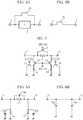
- FIG. 1 is a configuration diagram illustrating a switching circuit according to the present embodiment.
- the switching circuit illustrated in FIG. 1 includes a first terminal 1, a second terminal 2, a circuit element 3, a first switch 4, and a second switch 5.
- a signal source with an internal impedance Z 0 is connected with the first terminal 1, and a load with an impedance Z 0 is connected with the second terminal 2. Note that the signal source and the load are not illustrated.
- the first switch 4 is connected in parallel with the circuit element 3, and the second switch 5 is connected in series with the circuit element 3.
- a parallel circuit of the circuit element 3 and the first switch 4 is connected with the second terminal 2, and the second switch 5 is connected with the first terminal 1.
- the first switch 4 and the second switch 5 are switches controlled to be alternately on and off, and constituted by FETs such as MOS FETs or HEMTs, or MEMS switches. An on state of each of the switches will be expressed by an on-resistance and an off state thereof will be expressed by an off-capacitance.
- control is performed so that the second switch 5 is on and the first switch 4 is off in a first state.
- control is performed so that the second switch 5 is off and the first switch 4 is on.
- the on-resistances of the first switch 4 and the second switch 5 are R on4 ,R on5 ⁇ 0 (equally zero), which are deemed to be negligible, and the off-capacitances 4a and 5a are represented by C 4 and C 5 , respectively.
- An equivalent circuit of the first state in FIG. 1 is illustrated in FIG. 2A
- an equivalent circuit of the second state is illustrated in FIG. 2B .
- C 5 C 4 + 1 ⁇ 2 C 4 R 3 1 R 3 + 1 2 Z 0
- FETs or the like are used for the first switch 4 and the second switch 5 in the present embodiment, and one end of each switch may be a drain while the other end thereof may be a source, or conversely, one end may be a source and the other may be a drain.
- the first switch connected in parallel with the circuit element, and the second switch connected in series with the parallel circuit constituted by the circuit element and the first switch are included, and the first switch and the second switch alternately perform on-off operation, which enables reduction of a phase change at switching over a wide band.
- the switching circuit of the first embodiment because the first switch and the second switch each operate as a short circuit in the on state and obtain capacitance in the off state, the switching circuit is implemented with a simple configuration.
- the first switch and the second switch are switches each expressed by a resistor in the on state and an inductive parasitic element in the off state.
- FIG. 3 is a configuration diagram illustrating a switching circuit according to the second embodiment.
- the switching circuit illustrated in FIG. 3 includes a first terminal 1, a second terminal 2, a circuit element 3, a first switch 6, and a second switch 7.
- Each of the first switch 6 and the second switch 7 is a resistor in the on state and an inductive parasitic element in the off state, and the other components are similar to those in the first embodiment.
- the first switch 6 and the second switch 7 are constituted by MOS FETs, HEMTs, MEMS switches, or the like.
- control is performed so that the second switch 7 is on and the first switch 6 is off.
- control is performed so that the second switch 7 is off and the first switch 6 is on.
- the on-resistances of the first switch 6 and the second switch 7 are R on6 ,R on7 ⁇ 0 (equally zero), which are deemed to be negligible, and the inductive parasitic elements 6b and 7b in the off state are represented by L6 and L7, respectively.
- An equivalent circuit of the first state in FIG. 3 is illustrated in FIG. 4A
- an equivalent circuit of the second state is illustrated in FIG. 4B .
- L 6 L 7 is obtained, which enables reduction of phase fluctuation regardless of the frequency.
- FETs or the like are used for the switches in the present embodiment, and one end of each switch may be a drain while the other end thereof may be a source, or conversely, one end may be a source and the other may be a drain.
- the switching circuit of the second embodiment because the first switch and the second switch each operate as a short circuit in the on state and an inductor in the off state, the switching circuit is implemented with a simple configuration.
- the switching circuit of the first or second embodiment is used for two shunt circuits of a ⁇ -attenuator.
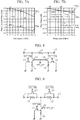
- FIG. 5 is a configuration diagram illustrating a variable attenuator according to the third embodiment.
- the variable attenuator illustrated in FIG. 5 includes a first terminal 11, a second terminal 12, a resistor 13, a third switch 14, second switches 15 and 18, resistors 16 and 19, and first switches 17 and 20.
- the first terminal 11 is an input terminal of the variable attenuator
- the second terminal 12 is an output terminal thereof.
- the resistor 13 is a series resistor of the ⁇ -attenuator, and is connected between the first terminal 11 and the second terminal 12.
- the third switch 14 is a switch connected in parallel with the resistor 13.
- the second switch 15 is a switch connected in series with a shunt through the first terminal 11, and corresponds to the second switch 5 of the first embodiment.
- the resistor 16 is connected in series with the second switch 15, and is a resistor corresponding to the circuit element 3 of the first embodiment.
- the first switch 17 is a switch connected with a shunt through a connecting point between the second switch 15 and the resistor 16 in parallel with the resistor 16, and corresponds to the first switch 4 of the first embodiment.
- the second switch 18 is a switch connected in series with a shunt through the second terminal 12, and corresponds to the second switch 5 of the first embodiment.
- the resistor 19 is a resistor connected in series with the second switch 18, and corresponding to the circuit element 3 of the first embodiment.
- the first switch 20 is a switch connected with a shunt through a connecting point between the second switch 18 and the resistor 19 in parallel with the resistor 19, and corresponds to the first switch 4 of the first embodiment.
- the switching circuit including the second switch 15, the resistor 16, and the first switch 17 and the switching circuit including the second switch 18, the resistor 19, and the first switch 20 are used for two shunt circuits of the ⁇ -attenuator.
- FETs are used for the third switch 14, the second switches 15 and 18, and the first switches 17 and 20, which are expressed by resistors in the on state and capacitive parasitic elements in the off state.
- the on-resistances in the on state are deemed to be negligible
- the parasitic capacitances in the off state are represented by 14a, 15a, 18a, 17a, and 20a
- the capacitance values thereof are C 14 , C 15 , C 18 , C 17 , and C 20 .
- the resistance values of the resistors 13, 16, and 19 are R 13 , R 16 , and R 19 .
- a switch using an FET uses connection between a drain terminal and a source terminal as a switch, and the drain terminal and the source terminal of the connection illustrated in FIG. 5 may be reversed.
- variable attenuator of the third embodiment having such a configuration
- the ⁇ -attenuator of the third embodiment is capable of switching to a first state in which an input signal is attenuated by the resistor 13, the resistor 16, and the resistor 19, and a second state in which the resistor 13 is short-circuited and the resistor 16 and the resistor 19 are disconnected from the first terminal 11 and the second terminal 12, respectively, so that an input signal is not attenuated.
- the second switches 15 and 18 are in the on state, and the third switch 14 and the first switches 17 and 20 are in the off state.
- the second switches 15 and 18 are in the off state, and the third switch 14 and the first switches 17 and 20 are in the on state.
- the resistor 13 typically has a low resistance
- its relation with the off-capacitance of the switch is R 13 ⁇ 1/ ⁇ C 14 .
- FIG. 6A An equivalent circuit of the first state is illustrated in FIG. 6A
- FIG. 6B An equivalent circuit of the second state is illustrated in FIG. 6B .
- the phase fluctuation in the first state and the second state can be reduced independently of the frequency.
- the capacitance does not affect the absolute value of the attenuation of the ⁇ -attenuator.
- FIG. 7 illustrates results of calculation when the attenuation is set to 3 dB in the equivalent circuits illustrated in FIG. 6 .
- FIG. 7A illustrates the pass characteristics
- FIG. 7B illustrates the pass phase.
- a characteristic 701a represents the first state
- a characteristic 702a represents the second state
- a characteristic 701b represents the first state
- a characteristic 702b represent the second state.
- the element value of the resistor 13 is 18 ⁇
- the element values of the resistor 16 and the resistor 19 are 274 ⁇
- the off-capacitance of the third switch 14 is 0.05 pF
- the off-capacitances of the second switches 15 and 18 and the first switches 17 and 20 are 0.1 pF.
- the pass characteristics of the second state and the first state are 3.04 dB at 2 GHz and 2.95 dB at 10 GHz, and the difference between the pass characteristics is equal to or less than 0.1 dB.
- the pass phase at 2 GHz is -3.4 deg in the second state and -3.6 deg in the first state
- the pass phase at 10 GHz is -17.6 deg in the second state and -16.8 deg in the first state
- the phase difference between the first and second states is thus reduced to equal to or smaller than 1 deg.
- the configuration of the third embodiment enables reduction of phase fluctuation over a five times wider band.
- variable attenuator of the third embodiment two shunt circuits of the ⁇ -attenuator are each replaced with the switching circuit of the first embodiment, a resistor is used for the circuit element of the switching circuit, the third switch is connected in parallel with the series resistor of the ⁇ -attenuator, the third switch is controlled to be off in the first state and to be on in the second state, the first switch is controlled to be off in the first state and to be on in the second state, and the second switch is controlled to be on in the first state and to be off in the second state, which enables reduction of phase change at switching over a wide band in the ⁇ -attenuator as well.
- a fourth embodiment is an example of a ⁇ type variable attenuator with a low attenuation.
- FIG. 8 illustrates a variable attenuator of the fourth embodiment.
- variable attenuator illustrated in FIG. 8 includes a first terminal 11, a second terminal 12, a resistor 13, second switches 15 and 18, resistors 16 and 19, and first switches 17 and 20.
- the variable attenuator of the fourth embodiment has the same configuration as that of the ⁇ type variable attenuator presented in the third embodiment except that the third switch 14 is not connected in parallel with the resistor 13 connected in series between the first terminal 11 and the second terminal 12.
- variable attenuator of the fourth embodiment operation of the variable attenuator of the fourth embodiment will be explained.
- the ⁇ type variable attenuator of the fourth embodiment is capable of switching to a first state in which an input signal is attenuated by the resistor 13, the resistor 16, and the resistor 19, and a second state in which an input signal is not attenuated.
- the first state the second switches 15 and 18 are in the on state, and the first switches 17 and 20 are in the off state.
- the second switches 15 and 18 are in the off state, and the first switches 17 and 20 are in the on state.
- the resistance value of the resistor 13 is several ohms ( ⁇ ), and thus the resistor 13 need not be short-circuited as in the third embodiment.
- Equivalent circuits of the first state and the second state are equivalent to those in FIGS. 6A and 6B except that the parasitic capacitance 14a in the off state of the third switch 14 is not present, and the phase fluctuation in the first state and the second state can thus be reduced independently of the frequency according to the principle of the configuration of the circuit connected with the shunt presented in the first embodiment and the formula (3).
- variable attenuator of the fourth embodiment two shunt circuits of the ⁇ -attenuator are each replaced with the switching circuit of the first embodiment, a resistor is used for the circuit element of the switching circuit, the first switch is controlled to be off in the first state and to be on in the second state, and the second switch is controlled to be on in the first state and to be off in the second state, which enables reduction of phase change at switching over a wide band in the ⁇ type variable attenuator with a low attenuation as well.
- the configuration of the first embodiment is used for the switching circuit in the third embodiment and the fourth embodiment described above, the configuration of the second embodiment may be used.
- the switching circuit of the first embodiment is used for a T type variable attenuator.
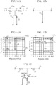
- FIG. 9 is a configuration diagram illustrating a variable attenuator according to the fifth embodiment.
- the variable attenuator illustrated in FIG. 9 includes a first terminal 11, a second terminal 12, resistors 21 and 22, a fourth switch 23, a fifth switch 24, a resistor 25, a second switch 26, and a first switch 27.
- the resistor 21 and the resistor 22 are connected in series between the first terminal 11 and the second terminal 12, the fourth switch 23 is connected in parallel with the resistor 21, and the fifth switch 24 is connected in parallel with the resistor 22.
- One end of the second switch 26 is connected with a connecting point of the resistor 21 and the resistor 22, and the resistor 25 and the first switch 27 are connected with the other end of the second switch 26.
- the other ends of the resistor 25 and the first switch 27 are grounded.
- the second switch 26 and the first switch 27 are switches corresponding to the second switch 5 and the first switch 4 of the first embodiment.
- a switching circuit constituted by the resistor 25, the second switch 26, and the first switch 27 is used for a shunt circuit of the T type variable attenuator.
- FETs are used for the fourth switch 23, the fifth switch 24, the second switch 26, and the first switch 27, which are expressed by resistors in the on state and capacitive parasitic elements in the off state.
- the on-resistances in the on state are deemed to be negligible
- the parasitic capacitances in the off state are represented by 23a, 24a, 26a, and 27a
- the capacitance values thereof are C 23 , C 24 , C 26 , and C 27 .
- the resistance values of the resistors 21, 22, and 25 are R 21 , R 22 , and R 25 .
- a switch using an FET uses between a drain terminal and a source terminal as a switch, and the drain terminal and the source terminal of the connection illustrated in FIG. 9 may be reversed.
- variable attenuator of the fifth embodiment operation of the variable attenuator of the fifth embodiment will be explained.
- the T type variable attenuator of the fifth embodiment is capable of switching to a first state in which an input signal is attenuated by the resistor 21, the resistor 22, and the resistor 25, and a second state in which the resistor 21 and the resistor 22 are short-circuited and the resistor 25 is disconnected from the first terminal 11 and the second terminal 12 so that an input signal is not attenuated.
- the second switch 26 In the first state, the second switch 26 is in the on state, and the fourth switch 23, the fifth switch 24, and the first switch 27 are in the off state.
- the second switch 26 is in the off state, and the fourth switch 23, the fifth switch 24, and the first switch 27 are in the on state.
- the relations thereof with the off-capacitances of the switches are R 21 ⁇ 1/j ⁇ C 23 and R 22 ⁇ 1/j ⁇ C 24 .
- FIG. 10A An equivalent circuit of the first state is illustrated in FIG. 10A
- FIG. 10B An equivalent circuit of the second state is illustrated in FIG. 10B .
- the phase fluctuation in the first state and the second state can be reduced independently of the frequency.
- the capacitance does not affect the absolute value of the attenuation of the T type variable attenuator.
- FIG. 11 illustrates results of calculation when the attenuation is set to 3 dB in the equivalent circuits illustrated in FIG. 9 .
- FIG. 11A illustrates the pass characteristics
- FIG. 11B illustrates the pass phase.
- a characteristic 1101a represents the first state
- a characteristic 1102a represents the second state
- a characteristic 1101b represents the first state
- a characteristic 1102b represents the second state.
- the element values of the resistor 21 and the resistor 22 are 9 ⁇
- the element value of the resistor 25 is 132 ⁇
- the off-capacitances of the fourth switch 23 and the fifth switch 24 are 0.05 pF
- the off-capacitances of the second switch 26 and the first switch 27 are 0.1 pF.
- the pass characteristics in the second state and the first state are 3.02 dB at 2 GHz and 3.01 dB at 10 GHz, and the difference between the pass characteristics is equal to or less than 0.1 dB.
- the pass phase at 2 GHz is -1.8 deg in the second state and -1.6 deg in the first state
- the pass phase at 10 GHz is -9.1 deg in the second state and -8.2 deg in the first state
- the phase difference between the first and second states is thus reduced to equal to or smaller than 1 deg.
- the configuration of the fifth embodiment enables reduction of phase fluctuation over a five times wider band.
- the shunt circuit of the T type attenuator is replaced with the switching circuit of the first embodiment, a resistor is used for the circuit element of the switching circuit, the fourth switch and the fifth switch are connected to be parallel to two series resistors of the T type attenuator, the fourth switch and the fifth switch are controlled to be off in the first state and to be on in the second state, the first switch is controlled to be off in the first state and to be on in the second state, and the second switch is controlled to be on in the first state and to be off in the second state, which enables reduction of phase change at switching over a wide band in the T type attenuator as well.
- a sixth embodiment is an example of a T type variable attenuator with a low attenuation.
- FIG. 12 illustrates a variable attenuator of the sixth embodiment.
- variable attenuator illustrated in FIG. 12 includes a first terminal 11, a second terminal 12, resistors 21 and 22, a resistor 25, a second switch 26, and a first switch 27.
- the variable attenuator of the sixth embodiment has the same configuration as that of the T type variable attenuator presented in the fifth embodiment except that the fourth switch 23 and the fifth switch 24 connected in parallel with the resistors 21 and 22, respectively, connected in series between the first terminal 11 and the second terminal 12 are not included.
- variable attenuator of the sixth embodiment operation of the variable attenuator of the sixth embodiment will be explained.
- the T type variable attenuator of the sixth embodiment is capable of switching to a first state in which an input signal is attenuated by the resistor 21, the resistor 22, and the resistor 25, and a second state in which an input signal is not attenuated.
- the first state the second switch 26 is in the on state, and the first switch 27 is in the off state.
- the second state the second switch 26 is in the off state, and the first switch 27 is in the on state.
- the resistance values of the resistors 21 and 22 are low, and thus the resistors 21 and 22 need not be short-circuited as in the fifth embodiment.
- Equivalent circuits of the first state and the second state are equivalent to those in FIGS. 10A and FIG. 10B except that the parasitic capacitance 23a in the off state of the fourth switch 23 and the parasitic capacitance 24a in the off state of the fifth switch 24 are not present.
- the phase fluctuation in the first state and the second state can be reduced independently of the frequency.
- the capacitance does not affect the absolute value of the attenuation of the T type variable attenuator. Thus, characteristics with different pass amplitudes, with the fluctuation of pass phase reduced, in the first state and the second state are achieved.
- the shunt circuit of the T type attenuator is replaced with the switching circuit of the first embodiment, a resistor is used for the circuit element of the switching circuit, the first switch is controlled to be off in the first state and to be on in the second state, and the second switch is controlled to be on in the first state and to be off in the second state, which enables reduction of phase change at switching over a wide band in the T type variable attenuator with a low attenuation as well.
- the configuration of the first embodiment is used for the switching circuit in the fifth embodiment and the sixth embodiment described above, the configuration of the second embodiment may be used.
- a switching circuit and a variable attenuator relates to a configuration in which switches having the same parasitic component are connected in series and in parallel with a circuit element, and controlled to be alternately on and off, which is particularly effectively applied to a circuit that needs to reduce phase change at switching over a wide band in a variable attenuator.
Landscapes
- Attenuators (AREA)
- Networks Using Active Elements (AREA)
- Electronic Switches (AREA)
Abstract
Description
- The present invention relates to a switching circuit in which a circuit element is connected in parallel or in series with a first switch and a second switch, which are controlled to be alternately on and off by the switching circuit, and to a variable attenuator including the switching circuit.
- For compensation for phase change caused by a parasitic element at switching, a switching circuit of related art loads an inductive element to resonate with a capacitive parasitic element, so that the influence of the parasitic element is cancelled, for example (refer to
Patent Literature 1, for example). - Patent Literature 1:
JP 2003-309454 A - Because resonance of the inductive element and the parasitic capacitance is used, however, the switching circuit of the related art has a problem of a narrow band.
- The present invention has been made to solve such problems as described above, and an object thereof is to provide a switching circuit capable of reducing phase change at switching over a wide band.
- A variable attenuator according to the invention includes a first switch connected in parallel with a circuit element, and a second switch connected in series with a parallel circuit constituted by the circuit element and the first switch, wherein the first switch and the second switch alternately perform on-off operation.
- In the variable attenuator according to the invention, switches are connected in series and in parallel with a circuit element, and alternately perform on-off operation. This enables reduction of phase change at switching over a wide band.
-
-
FIG. 1 is a configuration diagram illustrating a switching circuit according to a first embodiment of the invention. -
FIG. 2A is an equivalent circuit diagram illustrating operation in a first state of the switching circuit, andFIG. 2B is an equivalent circuit diagram illustrating operation in a second state of the switching circuit according to the first embodiment of the invention. -
FIG. 3 is a configuration diagram illustrating a switching circuit according to a second embodiment of the invention. -
FIG. 4A is an equivalent circuit diagram illustrating operation in a first state of the switching circuit, andFIG. 4B is an equivalent circuit diagram illustrating operation in a second state of the switching circuit according to the second embodiment of the invention. -
FIG. 5 is a configuration diagram illustrating a variable attenuator according to a third embodiment of the invention. -
FIG. 6A is an equivalent circuit diagram illustrating operation in a first state of the variable attenuator, andFIG. 6B is an equivalent circuit diagram illustrating operation in a second state of the variable attenuator according to the third embodiment of the invention. -
FIG. 7A is an explanatory graph illustrating pass characteristics of the variable attenuator according to the third embodiment of the invention, andFIG. 7B is an explanatory graph illustrating pass phases thereof. -
FIG. 8 is a configuration diagram illustrating a variable attenuator according to a fourth embodiment of the invention. -
FIG. 9 is a configuration diagram illustrating a variable attenuator according to a fifth embodiment of the invention. -
FIG. 10A is an equivalent circuit diagram illustrating operation in a first state of the variable attenuator, andFIG. 10B is an equivalent circuit diagram illustrating operation in a second state of the variable attenuator according to the fifth embodiment of the invention. -
FIG. 11A is an explanatory graph illustrating pass characteristics of the variable attenuator according to the fifth embodiment of the invention, andFIG. 11B is an explanatory graph illustrating pass phases thereof. -
FIG. 12 is a configuration diagram illustrating a variable attenuator according to a sixth embodiment of the invention. - Embodiments for carrying out the invention will now be described with reference to the accompanying drawings for more detailed explanation of the invention. First Embodiment.
-
FIG. 1 is a configuration diagram illustrating a switching circuit according to the present embodiment. - The switching circuit illustrated in
FIG. 1 includes afirst terminal 1, asecond terminal 2, acircuit element 3, afirst switch 4, and a second switch 5. A signal source with an internal impedance Z0 is connected with thefirst terminal 1, and a load with an impedance Z0 is connected with thesecond terminal 2. Note that the signal source and the load are not illustrated. Thefirst switch 4 is connected in parallel with thecircuit element 3, and the second switch 5 is connected in series with thecircuit element 3. A parallel circuit of thecircuit element 3 and thefirst switch 4 is connected with thesecond terminal 2, and the second switch 5 is connected with thefirst terminal 1. Thefirst switch 4 and the second switch 5 are switches controlled to be alternately on and off, and constituted by FETs such as MOS FETs or HEMTs, or MEMS switches. An on state of each of the switches will be expressed by an on-resistance and an off state thereof will be expressed by an off-capacitance. - Next, operation of the switching circuit having such a configuration will be explained.
- When a signal is input through the
first terminal 1, control is performed so that the second switch 5 is on and thefirst switch 4 is off in a first state. In contrast, in a second state, control is performed so that the second switch 5 is off and thefirst switch 4 is on. The on-resistances of thefirst switch 4 and the second switch 5 are Ron4,Ron5 ≈ 0 (equally zero), which are deemed to be negligible, and the off-capacitances FIG. 1 is illustrated inFIG. 2A , and an equivalent circuit of the second state is illustrated inFIG. 2B . - Calculation of the phase of a pass characteristic S21 in the first state of
FIG. 2A when the impedance Z3 of thecircuit element 3 is a resistance R3 is as follows.
- Calculation of the phase of the pass characteristic S21 in the second state of
FIG. 2B in a similar manner is as follows.
- A condition for reducing phase fluctuation in the first state and the second state is tanθ1 = tanθ2, and a condition to meet the condition is implemented by the formulas (1) and (2) as follows.

- At high frequencies or when R3 is a large value, C4=C5 is obtained, and meeting this condition enables reduction of phase fluctuation over a wide band regardless of the frequency.
- In a similar manner, when Z3 is a capacitance C3, a condition for reducing phase fluctuation is obtained as follows.

- Meeting the formula (4) enables reduction of phase fluctuation over a wide band regardless of the frequency.
- In a similar manner, when Z3 is an inductive element L3, a condition for reducing phase fluctuation is obtained as follows.

- At high frequencies or when L3 is a large value, meeting C4=C5 enables reduction of phase fluctuation over a wide band regardless of the frequency.
- Note that FETs or the like are used for the
first switch 4 and the second switch 5 in the present embodiment, and one end of each switch may be a drain while the other end thereof may be a source, or conversely, one end may be a source and the other may be a drain. - As described above, according to the switching circuit of the first embodiment, the first switch connected in parallel with the circuit element, and the second switch connected in series with the parallel circuit constituted by the circuit element and the first switch are included, and the first switch and the second switch alternately perform on-off operation, which enables reduction of a phase change at switching over a wide band.
- In addition, according to the switching circuit of the first embodiment, because the first switch and the second switch each operate as a short circuit in the on state and obtain capacitance in the off state, the switching circuit is implemented with a simple configuration.
- In a second embodiment, the first switch and the second switch are switches each expressed by a resistor in the on state and an inductive parasitic element in the off state.
-
FIG. 3 is a configuration diagram illustrating a switching circuit according to the second embodiment. The switching circuit illustrated inFIG. 3 includes afirst terminal 1, asecond terminal 2, acircuit element 3, afirst switch 6, and asecond switch 7. Each of thefirst switch 6 and thesecond switch 7 is a resistor in the on state and an inductive parasitic element in the off state, and the other components are similar to those in the first embodiment. Thefirst switch 6 and thesecond switch 7 are constituted by MOS FETs, HEMTs, MEMS switches, or the like. - Next, operation of the switching circuit of the second embodiment will be explained.
- In the first state, control is performed so that the
second switch 7 is on and thefirst switch 6 is off. In contrast, in the second state, control is performed so that thesecond switch 7 is off and thefirst switch 6 is on. The on-resistances of thefirst switch 6 and thesecond switch 7 are Ron6,Ron7 ≈ 0 (equally zero), which are deemed to be negligible, and the inductiveparasitic elements FIG. 3 is illustrated inFIG. 4A , and an equivalent circuit of the second state is illustrated inFIG. 4B . - Calculation of the phase of the pass characteristic S21 in the first state illustrated in
FIG. 4A when the impedance Z3 of thecircuit element 3 is a resistance R3 is as follows.
- Calculation of the phase of the pass characteristic S21 in the second state illustrated in
FIG. 4B in a similar manner is as follows.
- The following is sufficient for reducing phase fluctuation.

- A condition to meet this is obtained as follows by the formulas (6) and (7).

- At low frequencies or when R3 is sufficiently large, meeting L6=L7 enables reduction of phase fluctuation regardless of the frequency.
- In a similar manner, a condition for reducing phase fluctuation when Z3 is a capacitance (C3) is as follows:

- At low frequencies or when C3 is sufficiently small, L6 = L7 is obtained, which enables reduction of phase fluctuation regardless of the frequency.
- In a similar manner, a condition for reducing phase fluctuation when Z3 is an inductive element (L3) is as follows:

- This enables reduction of phase fluctuation regardless of the frequency.
- FETs or the like are used for the switches in the present embodiment, and one end of each switch may be a drain while the other end thereof may be a source, or conversely, one end may be a source and the other may be a drain.
- As described above, according to the switching circuit of the second embodiment, because the first switch and the second switch each operate as a short circuit in the on state and an inductor in the off state, the switching circuit is implemented with a simple configuration.
- In a third embodiment, the switching circuit of the first or second embodiment is used for two shunt circuits of a π-attenuator.
-
FIG. 5 is a configuration diagram illustrating a variable attenuator according to the third embodiment. The variable attenuator illustrated inFIG. 5 includes afirst terminal 11, asecond terminal 12, aresistor 13, athird switch 14, second switches 15 and 18,resistors first switches first terminal 11 is an input terminal of the variable attenuator, and thesecond terminal 12 is an output terminal thereof. Theresistor 13 is a series resistor of the π-attenuator, and is connected between thefirst terminal 11 and thesecond terminal 12. Thethird switch 14 is a switch connected in parallel with theresistor 13. Thesecond switch 15 is a switch connected in series with a shunt through thefirst terminal 11, and corresponds to the second switch 5 of the first embodiment. Theresistor 16 is connected in series with thesecond switch 15, and is a resistor corresponding to thecircuit element 3 of the first embodiment. Thefirst switch 17 is a switch connected with a shunt through a connecting point between thesecond switch 15 and theresistor 16 in parallel with theresistor 16, and corresponds to thefirst switch 4 of the first embodiment. Thesecond switch 18 is a switch connected in series with a shunt through thesecond terminal 12, and corresponds to the second switch 5 of the first embodiment. Theresistor 19 is a resistor connected in series with thesecond switch 18, and corresponding to thecircuit element 3 of the first embodiment. Thefirst switch 20 is a switch connected with a shunt through a connecting point between thesecond switch 18 and theresistor 19 in parallel with theresistor 19, and corresponds to thefirst switch 4 of the first embodiment. As described above, in the variable attenuator of the third embodiment, the switching circuit including thesecond switch 15, theresistor 16, and thefirst switch 17 and the switching circuit including thesecond switch 18, theresistor 19, and thefirst switch 20 are used for two shunt circuits of the π-attenuator. - FETs are used for the
third switch 14, thesecond switches first switches resistors FIG. 5 may be reversed. - Next, operation of the variable attenuator of the third embodiment having such a configuration will be explained.
- The π-attenuator of the third embodiment is capable of switching to a first state in which an input signal is attenuated by the
resistor 13, theresistor 16, and theresistor 19, and a second state in which theresistor 13 is short-circuited and theresistor 16 and theresistor 19 are disconnected from thefirst terminal 11 and thesecond terminal 12, respectively, so that an input signal is not attenuated. - In the first state, the
second switches third switch 14 and thefirst switches second switches third switch 14 and thefirst switches resistor 13 typically has a low resistance, its relation with the off-capacitance of the switch is R13 << 1/ωC14. - An equivalent circuit of the first state is illustrated in
FIG. 6A , and an equivalent circuit of the second state is illustrated inFIG. 6B . At higher frequencies or when the values of R16 and R19 are larger than those in the formula (3) of the first embodiment, the phase fluctuation in the first state and the second state can be reduced independently of the frequency. In addition, the capacitance does not affect the absolute value of the attenuation of the π-attenuator. Thus, characteristics with different pass amplitudes, with the fluctuation of pass phase reduced, in the first state and the second state are achieved. -
FIG. 7 illustrates results of calculation when the attenuation is set to 3 dB in the equivalent circuits illustrated inFIG. 6 .FIG. 7A illustrates the pass characteristics, andFIG. 7B illustrates the pass phase. InFIG. 7A , a characteristic 701a represents the first state, a characteristic 702a represents the second state. InFIG. 7B , a characteristic 701b represents the first state, and a characteristic 702b represent the second state. In the calculation, the element value of theresistor 13 is 18 Ω, the element values of theresistor 16 and theresistor 19 are 274 Ω, the off-capacitance of thethird switch 14 is 0.05 pF, and the off-capacitances of thesecond switches first switches - As described above, according to the variable attenuator of the third embodiment, two shunt circuits of the π-attenuator are each replaced with the switching circuit of the first embodiment, a resistor is used for the circuit element of the switching circuit, the third switch is connected in parallel with the series resistor of the π-attenuator, the third switch is controlled to be off in the first state and to be on in the second state, the first switch is controlled to be off in the first state and to be on in the second state, and the second switch is controlled to be on in the first state and to be off in the second state, which enables reduction of phase change at switching over a wide band in the π-attenuator as well.
- A fourth embodiment is an example of a π type variable attenuator with a low attenuation.
FIG. 8 illustrates a variable attenuator of the fourth embodiment. - The variable attenuator illustrated in
FIG. 8 includes afirst terminal 11, asecond terminal 12, aresistor 13, second switches 15 and 18,resistors first switches third switch 14 is not connected in parallel with theresistor 13 connected in series between thefirst terminal 11 and thesecond terminal 12. - Next, operation of the variable attenuator of the fourth embodiment will be explained.
- The π type variable attenuator of the fourth embodiment is capable of switching to a first state in which an input signal is attenuated by the
resistor 13, theresistor 16, and theresistor 19, and a second state in which an input signal is not attenuated. In the first state, thesecond switches first switches second switches first switches resistor 13 is several ohms (Ω), and thus theresistor 13 need not be short-circuited as in the third embodiment. Equivalent circuits of the first state and the second state are equivalent to those inFIGS. 6A and 6B except that theparasitic capacitance 14a in the off state of thethird switch 14 is not present, and the phase fluctuation in the first state and the second state can thus be reduced independently of the frequency according to the principle of the configuration of the circuit connected with the shunt presented in the first embodiment and the formula (3). - As described above, according to the variable attenuator of the fourth embodiment, two shunt circuits of the π-attenuator are each replaced with the switching circuit of the first embodiment, a resistor is used for the circuit element of the switching circuit, the first switch is controlled to be off in the first state and to be on in the second state, and the second switch is controlled to be on in the first state and to be off in the second state, which enables reduction of phase change at switching over a wide band in the π type variable attenuator with a low attenuation as well.
- While the configuration of the first embodiment is used for the switching circuit in the third embodiment and the fourth embodiment described above, the configuration of the second embodiment may be used.
- In a fifth embodiment, the switching circuit of the first embodiment is used for a T type variable attenuator.
-
FIG. 9 is a configuration diagram illustrating a variable attenuator according to the fifth embodiment. - The variable attenuator illustrated in
FIG. 9 includes afirst terminal 11, asecond terminal 12,resistors resistor 25, asecond switch 26, and afirst switch 27. Theresistor 21 and theresistor 22 are connected in series between thefirst terminal 11 and thesecond terminal 12, the fourth switch 23 is connected in parallel with theresistor 21, and the fifth switch 24 is connected in parallel with theresistor 22. One end of thesecond switch 26 is connected with a connecting point of theresistor 21 and theresistor 22, and theresistor 25 and thefirst switch 27 are connected with the other end of thesecond switch 26. In addition, the other ends of theresistor 25 and thefirst switch 27 are grounded. Thesecond switch 26 and thefirst switch 27 are switches corresponding to the second switch 5 and thefirst switch 4 of the first embodiment. Thus, in the variable attenuator of the fifth embodiment, a switching circuit constituted by theresistor 25, thesecond switch 26, and thefirst switch 27 is used for a shunt circuit of the T type variable attenuator. - FETs are used for the fourth switch 23, the fifth switch 24, the
second switch 26, and thefirst switch 27, which are expressed by resistors in the on state and capacitive parasitic elements in the off state. The on-resistances in the on state are deemed to be negligible, the parasitic capacitances in the off state are represented by 23a, 24a, 26a, and 27a, and the capacitance values thereof are C23, C24, C26, and C27. In addition, the resistance values of theresistors FIG. 9 may be reversed. - Next, operation of the variable attenuator of the fifth embodiment will be explained.
- The T type variable attenuator of the fifth embodiment is capable of switching to a first state in which an input signal is attenuated by the
resistor 21, theresistor 22, and theresistor 25, and a second state in which theresistor 21 and theresistor 22 are short-circuited and theresistor 25 is disconnected from thefirst terminal 11 and thesecond terminal 12 so that an input signal is not attenuated. In the first state, thesecond switch 26 is in the on state, and the fourth switch 23, the fifth switch 24, and thefirst switch 27 are in the off state. In the second state, thesecond switch 26 is in the off state, and the fourth switch 23, the fifth switch 24, and thefirst switch 27 are in the on state. In addition, in the T type attenuator, because theresistor 21 and theresistor 22 typically have low resistances, the relations thereof with the off-capacitances of the switches are R21 << 1/jωC23 and R22 << 1/jωC24. - An equivalent circuit of the first state is illustrated in
FIG. 10A , and an equivalent circuit of the second state is illustrated inFIG. 10B . At higher frequencies or when the value of R25 is larger than those in the formula (3) of the first embodiment, the phase fluctuation in the first state and the second state can be reduced independently of the frequency. In addition, the capacitance does not affect the absolute value of the attenuation of the T type variable attenuator. Thus, characteristics with different pass amplitudes, with the fluctuation of pass phase reduced, in the first state and the second state are achieved. -
FIG. 11 illustrates results of calculation when the attenuation is set to 3 dB in the equivalent circuits illustrated inFIG. 9 .FIG. 11A illustrates the pass characteristics, andFIG. 11B illustrates the pass phase. InFIG. 11A , a characteristic 1101a represents the first state, and a characteristic 1102a represents the second state. InFIG. 11B , a characteristic 1101b represents the first state, and a characteristic 1102b represents the second state. - In the calculation, the element values of the
resistor 21 and theresistor 22 are 9 Ω, the element value of theresistor 25 is 132 Ω, the off-capacitances of the fourth switch 23 and the fifth switch 24 are 0.05 pF, and the off-capacitances of thesecond switch 26 and thefirst switch 27 are 0.1 pF. The pass characteristics in the second state and the first state are 3.02 dB at 2 GHz and 3.01 dB at 10 GHz, and the difference between the pass characteristics is equal to or less than 0.1 dB. In a similar manner, the pass phase at 2 GHz is -1.8 deg in the second state and -1.6 deg in the first state, the pass phase at 10 GHz is -9.1 deg in the second state and -8.2 deg in the first state, and the phase difference between the first and second states is thus reduced to equal to or smaller than 1 deg. In this manner, the configuration of the fifth embodiment enables reduction of phase fluctuation over a five times wider band. - As described above, according to the variable attenuator of the fifth embodiment, the shunt circuit of the T type attenuator is replaced with the switching circuit of the first embodiment, a resistor is used for the circuit element of the switching circuit, the fourth switch and the fifth switch are connected to be parallel to two series resistors of the T type attenuator, the fourth switch and the fifth switch are controlled to be off in the first state and to be on in the second state, the first switch is controlled to be off in the first state and to be on in the second state, and the second switch is controlled to be on in the first state and to be off in the second state, which enables reduction of phase change at switching over a wide band in the T type attenuator as well.
- A sixth embodiment is an example of a T type variable attenuator with a low attenuation.
FIG. 12 illustrates a variable attenuator of the sixth embodiment. - The variable attenuator illustrated in
FIG. 12 includes afirst terminal 11, asecond terminal 12,resistors resistor 25, asecond switch 26, and afirst switch 27. In other words, the variable attenuator of the sixth embodiment has the same configuration as that of the T type variable attenuator presented in the fifth embodiment except that the fourth switch 23 and the fifth switch 24 connected in parallel with theresistors first terminal 11 and thesecond terminal 12 are not included. - Next, operation of the variable attenuator of the sixth embodiment will be explained.
- The T type variable attenuator of the sixth embodiment is capable of switching to a first state in which an input signal is attenuated by the
resistor 21, theresistor 22, and theresistor 25, and a second state in which an input signal is not attenuated. In the first state, thesecond switch 26 is in the on state, and thefirst switch 27 is in the off state. In the second state, thesecond switch 26 is in the off state, and thefirst switch 27 is in the on state. - When the attenuation in the first state is low, the resistance values of the
resistors resistors FIGS. 10A and FIG. 10B except that theparasitic capacitance 23a in the off state of the fourth switch 23 and theparasitic capacitance 24a in the off state of the fifth switch 24 are not present. At higher frequencies or when the value of R25 is larger than those in the formula (3) of the first embodiment, the phase fluctuation in the first state and the second state can be reduced independently of the frequency. In addition, the capacitance does not affect the absolute value of the attenuation of the T type variable attenuator. Thus, characteristics with different pass amplitudes, with the fluctuation of pass phase reduced, in the first state and the second state are achieved. - As described above, according to the variable attenuator of the sixth embodiment, the shunt circuit of the T type attenuator is replaced with the switching circuit of the first embodiment, a resistor is used for the circuit element of the switching circuit, the first switch is controlled to be off in the first state and to be on in the second state, and the second switch is controlled to be on in the first state and to be off in the second state, which enables reduction of phase change at switching over a wide band in the T type variable attenuator with a low attenuation as well.
- While the configuration of the first embodiment is used for the switching circuit in the fifth embodiment and the sixth embodiment described above, the configuration of the second embodiment may be used.
- The embodiments of the present invention can be freely combined, any components in the embodiments can be modified, and any components in the embodiments can be omitted within the scope of the invention.
- As described above, a switching circuit and a variable attenuator according to the present invention relates to a configuration in which switches having the same parasitic component are connected in series and in parallel with a circuit element, and controlled to be alternately on and off, which is particularly effectively applied to a circuit that needs to reduce phase change at switching over a wide band in a variable attenuator.
- 1, 11: first terminal, 2, 12: second terminal, 3: circuit element, 4, 6, 17, 20, 27: first switch, 5, 7, 15, 18, 26: second switch, 13, 16, 19, 21, 22, 25: resistor, 14: third switch, 23: fourth switch, 24: fifth switch
Claims (7)
- A switching circuit comprising:a first switch connected in parallel with a circuit element; anda second switch connected in series with a parallel circuit constituted by the circuit element and the first switch,wherein the first switch and the second switch alternately perform on-off operation.
- The switching circuit according to claim 1, wherein the first switch and the second switch each operate as a short circuit while being on and as capacitance while being off.
- The switching circuit according to claim 1, wherein the first switch and the second switch each operate as a short circuit while being on and as an inductor while being off.
- A variable attenuator, wherein
two shunt circuits of a π-attenuator are each replaced with the switching circuit according to any one of claims 1 to 3, a resistor is used for the circuit element of the switching circuit, and a third switch is connected in parallel with a series resistor of the π-attenuator,
the third switch is controlled to be off in a first state and to be on in a second state,
the first switch is controlled to be off in the first state and to be on in the second state, and
the second switch is controlled to be on in the first state and to be off in the second state. - A variable attenuator, wherein
two shunt circuits of a π-attenuator are each replaced with the switching circuit according to any one of claims 1 to 3, and a resistor is used for the circuit element of the switching circuit,
the first switch is controlled to be off in the first state and to be on in the second state, and
the second switch is controlled to be on in the first state and to be off in the second state. - A variable attenuator, wherein
a shunt circuit of a T type attenuator is replaced with the switching circuit according to any one of claims 1 to 3, a resistor is used for the circuit element of the switching circuit, and a fourth switch and a fifth switch are connected in parallel with one of two series resistors of the T type attenuator,
the fourth switch and the fifth switch are controlled to be off in a first state and to be on in a second state,
the first switch is controlled to be off in the first state and to be on in the second state, and
the second switch is controlled to be on in the first state and to be off in the second state. - A variable attenuator, wherein
a shunt circuit of a T type attenuator is replaced with the switching circuit according to any one of claims 1 to 3, and a resistor is used for the circuit element of the switching circuit,
the first switch is controlled to be off in the first state and to be on in the second state, and
the second switch is controlled to be on in the first state and to be off in the second state.
Applications Claiming Priority (1)
| Application Number | Priority Date | Filing Date | Title |
|---|---|---|---|
| PCT/JP2018/013299 WO2019186913A1 (en) | 2018-03-29 | 2018-03-29 | Switching circuit and variable attenuator |
Publications (3)
| Publication Number | Publication Date |
|---|---|
| EP3758225A1 true EP3758225A1 (en) | 2020-12-30 |
| EP3758225A4 EP3758225A4 (en) | 2021-03-10 |
| EP3758225B1 EP3758225B1 (en) | 2023-05-03 |
Family
ID=65020486
Family Applications (1)
| Application Number | Title | Priority Date | Filing Date |
|---|---|---|---|
| EP18912940.6A Active EP3758225B1 (en) | 2018-03-29 | 2018-03-29 | Switching circuit and variable attenuator |
Country Status (4)
| Country | Link |
|---|---|
| US (1) | US11451208B2 (en) |
| EP (1) | EP3758225B1 (en) |
| JP (1) | JP6452917B1 (en) |
| WO (1) | WO2019186913A1 (en) |
Families Citing this family (2)
| Publication number | Priority date | Publication date | Assignee | Title |
|---|---|---|---|---|
| CN113162581B (en) * | 2021-03-22 | 2022-08-05 | 中国电子科技集团公司第十三研究所 | Broadband digital phase shifter based on GaN HEMT device |
| US12095435B2 (en) * | 2022-06-13 | 2024-09-17 | Fujikura Ltd. | High frequency variable attenuation circuit |
Family Cites Families (11)
| Publication number | Priority date | Publication date | Assignee | Title |
|---|---|---|---|---|
| JPH0288303U (en) | 1988-12-27 | 1990-07-12 | ||
| US5666089A (en) * | 1996-04-12 | 1997-09-09 | Hewlett-Packard Company | Monolithic step attenuator having internal frequency compensation |
| JPH1155059A (en) * | 1997-07-29 | 1999-02-26 | Mitsubishi Electric Corp | Variable attenuator |
| JP4214710B2 (en) | 2002-04-15 | 2009-01-28 | 三菱電機株式会社 | Variable attenuator |
| JP4935373B2 (en) * | 2007-01-23 | 2012-05-23 | 横河電機株式会社 | Switch circuit and step attenuator using the switch circuit |
| JP5034925B2 (en) * | 2007-12-20 | 2012-09-26 | 株式会社デンソー | Switch circuit |
| KR101030050B1 (en) * | 2009-12-14 | 2011-04-21 | 한국과학기술원 | Digital Attenuator with Low Phase Shift |
| US8674746B1 (en) * | 2012-10-16 | 2014-03-18 | Freescale Semiconductor, Inc. | Electronic circuits with variable attenuators and methods of their operation |
| JP6076193B2 (en) * | 2013-05-20 | 2017-02-08 | 三菱電機株式会社 | Phase shift circuit |
| US10530320B2 (en) * | 2016-07-15 | 2020-01-07 | Psemi Corporation | Attenuator de-Qing loss improvement and phase balance |
| US20180062622A1 (en) * | 2016-08-30 | 2018-03-01 | Skyworks Solutions, Inc. | Binary-weighted attenuator having compensation circuit |
-
2018
- 2018-03-29 WO PCT/JP2018/013299 patent/WO2019186913A1/en not_active Ceased
- 2018-03-29 EP EP18912940.6A patent/EP3758225B1/en active Active
- 2018-03-29 JP JP2018547487A patent/JP6452917B1/en active Active
-
2020
- 2020-09-09 US US17/015,978 patent/US11451208B2/en active Active
Also Published As
| Publication number | Publication date |
|---|---|
| JP6452917B1 (en) | 2019-01-16 |
| WO2019186913A1 (en) | 2019-10-03 |
| EP3758225B1 (en) | 2023-05-03 |
| JPWO2019186913A1 (en) | 2020-04-30 |
| US11451208B2 (en) | 2022-09-20 |
| US20200412321A1 (en) | 2020-12-31 |
| EP3758225A4 (en) | 2021-03-10 |
Similar Documents
| Publication | Publication Date | Title |
|---|---|---|
| US9209801B2 (en) | High frequency switch circuit including gate bias resistances | |
| US9543630B2 (en) | Electronic device | |
| CN104852713A (en) | Switching controller | |
| US9419586B2 (en) | Device for negative group delay | |
| EP3952106A2 (en) | A resonator circuit | |
| US8552782B1 (en) | Quadrature phase network | |
| US20150349739A1 (en) | Common mode noise suppressing device | |
| US11451208B2 (en) | Switching circuit and variable attenuator | |
| US9419582B2 (en) | Filter device and duplexer | |
| US8981882B2 (en) | Electronic switch and communication device including such a switch | |
| CN112511132A (en) | Millimeter wave filtering frequency-selecting component and integrated circuit | |
| US8797097B2 (en) | Filtering device with low-pass filtering function and band-pass filtering function | |
| US10200031B2 (en) | Electronically switchable diplexer | |
| CN113746445B (en) | Directional coupler | |
| US10027305B1 (en) | Filter including non-magnetic frequency selective limiters | |
| JPH11234063A (en) | High frequency amplifier | |
| CN111384908B (en) | Power divider circuit, power divider and design method of power divider circuit | |
| CN110247635B (en) | Variable attenuator | |
| Kumngern | Electronically tunable current-mode universal biquadratic filter using a single CCCFTA | |
| JP4826536B2 (en) | Phase shift circuit | |
| EP3373455B1 (en) | High frequency switch | |
| US12143103B2 (en) | Multi-coil coupling-type single-pole four-throw switch and radio frequency integrated circuit | |
| US11146248B1 (en) | High linearity RF circuit and method for improving linearity thereof | |
| JP4410129B2 (en) | Frequency variable impedance matching circuit | |
| JP2011244187A (en) | Band variable filter |
Legal Events
| Date | Code | Title | Description |
|---|---|---|---|
| STAA | Information on the status of an ep patent application or granted ep patent |
Free format text: STATUS: THE INTERNATIONAL PUBLICATION HAS BEEN MADE |
|
| PUAI | Public reference made under article 153(3) epc to a published international application that has entered the european phase |
Free format text: ORIGINAL CODE: 0009012 |
|
| STAA | Information on the status of an ep patent application or granted ep patent |
Free format text: STATUS: REQUEST FOR EXAMINATION WAS MADE |
|
| 17P | Request for examination filed |
Effective date: 20200922 |
|
| AK | Designated contracting states |
Kind code of ref document: A1 Designated state(s): AL AT BE BG CH CY CZ DE DK EE ES FI FR GB GR HR HU IE IS IT LI LT LU LV MC MK MT NL NO PL PT RO RS SE SI SK SM TR |
|
| AX | Request for extension of the european patent |
Extension state: BA ME |
|
| A4 | Supplementary search report drawn up and despatched |
Effective date: 20210205 |
|
| RIC1 | Information provided on ipc code assigned before grant |
Ipc: H03K 17/04 20060101AFI20210201BHEP Ipc: H03H 11/24 20060101ALI20210201BHEP Ipc: H03K 17/693 20060101ALI20210201BHEP Ipc: H04B 1/44 20060101ALI20210201BHEP |
|
| DAV | Request for validation of the european patent (deleted) | ||
| DAX | Request for extension of the european patent (deleted) | ||
| STAA | Information on the status of an ep patent application or granted ep patent |
Free format text: STATUS: EXAMINATION IS IN PROGRESS |
|
| 17Q | First examination report despatched |
Effective date: 20211110 |
|
| GRAP | Despatch of communication of intention to grant a patent |
Free format text: ORIGINAL CODE: EPIDOSNIGR1 |
|
| STAA | Information on the status of an ep patent application or granted ep patent |
Free format text: STATUS: GRANT OF PATENT IS INTENDED |
|
| INTG | Intention to grant announced |
Effective date: 20220610 |
|
| GRAJ | Information related to disapproval of communication of intention to grant by the applicant or resumption of examination proceedings by the epo deleted |
Free format text: ORIGINAL CODE: EPIDOSDIGR1 |
|
| STAA | Information on the status of an ep patent application or granted ep patent |
Free format text: STATUS: EXAMINATION IS IN PROGRESS |
|
| INTC | Intention to grant announced (deleted) | ||
| GRAS | Grant fee paid |
Free format text: ORIGINAL CODE: EPIDOSNIGR3 |
|
| STAA | Information on the status of an ep patent application or granted ep patent |
Free format text: STATUS: GRANT OF PATENT IS INTENDED |
|
| GRAP | Despatch of communication of intention to grant a patent |
Free format text: ORIGINAL CODE: EPIDOSNIGR1 |
|
| INTG | Intention to grant announced |
Effective date: 20221118 |
|
| GRAA | (expected) grant |
Free format text: ORIGINAL CODE: 0009210 |
|
| STAA | Information on the status of an ep patent application or granted ep patent |
Free format text: STATUS: THE PATENT HAS BEEN GRANTED |
|
| AK | Designated contracting states |
Kind code of ref document: B1 Designated state(s): AL AT BE BG CH CY CZ DE DK EE ES FI FR GB GR HR HU IE IS IT LI LT LU LV MC MK MT NL NO PL PT RO RS SE SI SK SM TR |
|
| REG | Reference to a national code |
Ref country code: GB Ref legal event code: FG4D |
|
| REG | Reference to a national code |
Ref country code: AT Ref legal event code: REF Ref document number: 1565541 Country of ref document: AT Kind code of ref document: T Effective date: 20230515 Ref country code: CH Ref legal event code: EP |
|
| REG | Reference to a national code |
Ref country code: DE Ref legal event code: R096 Ref document number: 602018049434 Country of ref document: DE |
|
| REG | Reference to a national code |
Ref country code: IE Ref legal event code: FG4D |
|
| P01 | Opt-out of the competence of the unified patent court (upc) registered |
Effective date: 20230518 |
|
| REG | Reference to a national code |
Ref country code: LT Ref legal event code: MG9D |
|
| REG | Reference to a national code |
Ref country code: NL Ref legal event code: MP Effective date: 20230503 |
|
| REG | Reference to a national code |
Ref country code: AT Ref legal event code: MK05 Ref document number: 1565541 Country of ref document: AT Kind code of ref document: T Effective date: 20230503 |
|
| PG25 | Lapsed in a contracting state [announced via postgrant information from national office to epo] |
Ref country code: SE Free format text: LAPSE BECAUSE OF FAILURE TO SUBMIT A TRANSLATION OF THE DESCRIPTION OR TO PAY THE FEE WITHIN THE PRESCRIBED TIME-LIMIT Effective date: 20230503 Ref country code: PT Free format text: LAPSE BECAUSE OF FAILURE TO SUBMIT A TRANSLATION OF THE DESCRIPTION OR TO PAY THE FEE WITHIN THE PRESCRIBED TIME-LIMIT Effective date: 20230904 Ref country code: NO Free format text: LAPSE BECAUSE OF FAILURE TO SUBMIT A TRANSLATION OF THE DESCRIPTION OR TO PAY THE FEE WITHIN THE PRESCRIBED TIME-LIMIT Effective date: 20230803 Ref country code: NL Free format text: LAPSE BECAUSE OF FAILURE TO SUBMIT A TRANSLATION OF THE DESCRIPTION OR TO PAY THE FEE WITHIN THE PRESCRIBED TIME-LIMIT Effective date: 20230503 Ref country code: ES Free format text: LAPSE BECAUSE OF FAILURE TO SUBMIT A TRANSLATION OF THE DESCRIPTION OR TO PAY THE FEE WITHIN THE PRESCRIBED TIME-LIMIT Effective date: 20230503 Ref country code: AT Free format text: LAPSE BECAUSE OF FAILURE TO SUBMIT A TRANSLATION OF THE DESCRIPTION OR TO PAY THE FEE WITHIN THE PRESCRIBED TIME-LIMIT Effective date: 20230503 |
|
| PG25 | Lapsed in a contracting state [announced via postgrant information from national office to epo] |
Ref country code: RS Free format text: LAPSE BECAUSE OF FAILURE TO SUBMIT A TRANSLATION OF THE DESCRIPTION OR TO PAY THE FEE WITHIN THE PRESCRIBED TIME-LIMIT Effective date: 20230503 Ref country code: PL Free format text: LAPSE BECAUSE OF FAILURE TO SUBMIT A TRANSLATION OF THE DESCRIPTION OR TO PAY THE FEE WITHIN THE PRESCRIBED TIME-LIMIT Effective date: 20230503 Ref country code: LV Free format text: LAPSE BECAUSE OF FAILURE TO SUBMIT A TRANSLATION OF THE DESCRIPTION OR TO PAY THE FEE WITHIN THE PRESCRIBED TIME-LIMIT Effective date: 20230503 Ref country code: LT Free format text: LAPSE BECAUSE OF FAILURE TO SUBMIT A TRANSLATION OF THE DESCRIPTION OR TO PAY THE FEE WITHIN THE PRESCRIBED TIME-LIMIT Effective date: 20230503 Ref country code: IS Free format text: LAPSE BECAUSE OF FAILURE TO SUBMIT A TRANSLATION OF THE DESCRIPTION OR TO PAY THE FEE WITHIN THE PRESCRIBED TIME-LIMIT Effective date: 20230903 Ref country code: HR Free format text: LAPSE BECAUSE OF FAILURE TO SUBMIT A TRANSLATION OF THE DESCRIPTION OR TO PAY THE FEE WITHIN THE PRESCRIBED TIME-LIMIT Effective date: 20230503 Ref country code: GR Free format text: LAPSE BECAUSE OF FAILURE TO SUBMIT A TRANSLATION OF THE DESCRIPTION OR TO PAY THE FEE WITHIN THE PRESCRIBED TIME-LIMIT Effective date: 20230804 |
|
| PG25 | Lapsed in a contracting state [announced via postgrant information from national office to epo] |
Ref country code: FI Free format text: LAPSE BECAUSE OF FAILURE TO SUBMIT A TRANSLATION OF THE DESCRIPTION OR TO PAY THE FEE WITHIN THE PRESCRIBED TIME-LIMIT Effective date: 20230503 |
|
| PG25 | Lapsed in a contracting state [announced via postgrant information from national office to epo] |
Ref country code: SK Free format text: LAPSE BECAUSE OF FAILURE TO SUBMIT A TRANSLATION OF THE DESCRIPTION OR TO PAY THE FEE WITHIN THE PRESCRIBED TIME-LIMIT Effective date: 20230503 |
|
| PG25 | Lapsed in a contracting state [announced via postgrant information from national office to epo] |
Ref country code: SM Free format text: LAPSE BECAUSE OF FAILURE TO SUBMIT A TRANSLATION OF THE DESCRIPTION OR TO PAY THE FEE WITHIN THE PRESCRIBED TIME-LIMIT Effective date: 20230503 Ref country code: SK Free format text: LAPSE BECAUSE OF FAILURE TO SUBMIT A TRANSLATION OF THE DESCRIPTION OR TO PAY THE FEE WITHIN THE PRESCRIBED TIME-LIMIT Effective date: 20230503 Ref country code: RO Free format text: LAPSE BECAUSE OF FAILURE TO SUBMIT A TRANSLATION OF THE DESCRIPTION OR TO PAY THE FEE WITHIN THE PRESCRIBED TIME-LIMIT Effective date: 20230503 Ref country code: EE Free format text: LAPSE BECAUSE OF FAILURE TO SUBMIT A TRANSLATION OF THE DESCRIPTION OR TO PAY THE FEE WITHIN THE PRESCRIBED TIME-LIMIT Effective date: 20230503 Ref country code: DK Free format text: LAPSE BECAUSE OF FAILURE TO SUBMIT A TRANSLATION OF THE DESCRIPTION OR TO PAY THE FEE WITHIN THE PRESCRIBED TIME-LIMIT Effective date: 20230503 Ref country code: CZ Free format text: LAPSE BECAUSE OF FAILURE TO SUBMIT A TRANSLATION OF THE DESCRIPTION OR TO PAY THE FEE WITHIN THE PRESCRIBED TIME-LIMIT Effective date: 20230503 |
|
| REG | Reference to a national code |
Ref country code: DE Ref legal event code: R097 Ref document number: 602018049434 Country of ref document: DE |
|
| PLBE | No opposition filed within time limit |
Free format text: ORIGINAL CODE: 0009261 |
|
| STAA | Information on the status of an ep patent application or granted ep patent |
Free format text: STATUS: NO OPPOSITION FILED WITHIN TIME LIMIT |
|
| 26N | No opposition filed |
Effective date: 20240206 |
|
| PG25 | Lapsed in a contracting state [announced via postgrant information from national office to epo] |
Ref country code: SI Free format text: LAPSE BECAUSE OF FAILURE TO SUBMIT A TRANSLATION OF THE DESCRIPTION OR TO PAY THE FEE WITHIN THE PRESCRIBED TIME-LIMIT Effective date: 20230503 |
|
| PG25 | Lapsed in a contracting state [announced via postgrant information from national office to epo] |
Ref country code: SI Free format text: LAPSE BECAUSE OF FAILURE TO SUBMIT A TRANSLATION OF THE DESCRIPTION OR TO PAY THE FEE WITHIN THE PRESCRIBED TIME-LIMIT Effective date: 20230503 Ref country code: IT Free format text: LAPSE BECAUSE OF FAILURE TO SUBMIT A TRANSLATION OF THE DESCRIPTION OR TO PAY THE FEE WITHIN THE PRESCRIBED TIME-LIMIT Effective date: 20230503 |
|
| REG | Reference to a national code |
Ref country code: CH Ref legal event code: PL |
|
| PG25 | Lapsed in a contracting state [announced via postgrant information from national office to epo] |
Ref country code: BG Free format text: LAPSE BECAUSE OF FAILURE TO SUBMIT A TRANSLATION OF THE DESCRIPTION OR TO PAY THE FEE WITHIN THE PRESCRIBED TIME-LIMIT Effective date: 20230503 |
|
| PG25 | Lapsed in a contracting state [announced via postgrant information from national office to epo] |
Ref country code: LU Free format text: LAPSE BECAUSE OF NON-PAYMENT OF DUE FEES Effective date: 20240329 |
|
| PG25 | Lapsed in a contracting state [announced via postgrant information from national office to epo] |
Ref country code: MC Free format text: LAPSE BECAUSE OF FAILURE TO SUBMIT A TRANSLATION OF THE DESCRIPTION OR TO PAY THE FEE WITHIN THE PRESCRIBED TIME-LIMIT Effective date: 20230503 |
|
| PG25 | Lapsed in a contracting state [announced via postgrant information from national office to epo] |
Ref country code: MC Free format text: LAPSE BECAUSE OF FAILURE TO SUBMIT A TRANSLATION OF THE DESCRIPTION OR TO PAY THE FEE WITHIN THE PRESCRIBED TIME-LIMIT Effective date: 20230503 Ref country code: LU Free format text: LAPSE BECAUSE OF NON-PAYMENT OF DUE FEES Effective date: 20240329 Ref country code: BG Free format text: LAPSE BECAUSE OF FAILURE TO SUBMIT A TRANSLATION OF THE DESCRIPTION OR TO PAY THE FEE WITHIN THE PRESCRIBED TIME-LIMIT Effective date: 20230503 |
|
| REG | Reference to a national code |
Ref country code: BE Ref legal event code: MM Effective date: 20240331 |
|
| PG25 | Lapsed in a contracting state [announced via postgrant information from national office to epo] |
Ref country code: BE Free format text: LAPSE BECAUSE OF NON-PAYMENT OF DUE FEES Effective date: 20240331 |
|
| PG25 | Lapsed in a contracting state [announced via postgrant information from national office to epo] |
Ref country code: IE Free format text: LAPSE BECAUSE OF NON-PAYMENT OF DUE FEES Effective date: 20240329 |
|
| PG25 | Lapsed in a contracting state [announced via postgrant information from national office to epo] |
Ref country code: IE Free format text: LAPSE BECAUSE OF NON-PAYMENT OF DUE FEES Effective date: 20240329 Ref country code: BE Free format text: LAPSE BECAUSE OF NON-PAYMENT OF DUE FEES Effective date: 20240331 Ref country code: CH Free format text: LAPSE BECAUSE OF NON-PAYMENT OF DUE FEES Effective date: 20240331 |
|
| REG | Reference to a national code |
Ref country code: DE Ref legal event code: R084 Ref document number: 602018049434 Country of ref document: DE |
|
| PG25 | Lapsed in a contracting state [announced via postgrant information from national office to epo] |
Ref country code: CY Free format text: LAPSE BECAUSE OF FAILURE TO SUBMIT A TRANSLATION OF THE DESCRIPTION OR TO PAY THE FEE WITHIN THE PRESCRIBED TIME-LIMIT; INVALID AB INITIO Effective date: 20180329 |
|
| REG | Reference to a national code |
Ref country code: GB Ref legal event code: 746 Effective date: 20250804 |
|
| PG25 | Lapsed in a contracting state [announced via postgrant information from national office to epo] |
Ref country code: HU Free format text: LAPSE BECAUSE OF FAILURE TO SUBMIT A TRANSLATION OF THE DESCRIPTION OR TO PAY THE FEE WITHIN THE PRESCRIBED TIME-LIMIT; INVALID AB INITIO Effective date: 20180329 |
|
| PG25 | Lapsed in a contracting state [announced via postgrant information from national office to epo] |
Ref country code: TR Free format text: LAPSE BECAUSE OF FAILURE TO SUBMIT A TRANSLATION OF THE DESCRIPTION OR TO PAY THE FEE WITHIN THE PRESCRIBED TIME-LIMIT Effective date: 20230503 |
|
| PGFP | Annual fee paid to national office [announced via postgrant information from national office to epo] |
Ref country code: GB Payment date: 20260209 Year of fee payment: 9 |
|
| PGFP | Annual fee paid to national office [announced via postgrant information from national office to epo] |
Ref country code: DE Payment date: 20260204 Year of fee payment: 9 |
|
| PGFP | Annual fee paid to national office [announced via postgrant information from national office to epo] |
Ref country code: FR Payment date: 20260209 Year of fee payment: 9 |