EP3758046A1 - Method for combining silicon material and iii-v material, and associated device - Google Patents
Method for combining silicon material and iii-v material, and associated device Download PDFInfo
- Publication number
- EP3758046A1 EP3758046A1 EP19305873.2A EP19305873A EP3758046A1 EP 3758046 A1 EP3758046 A1 EP 3758046A1 EP 19305873 A EP19305873 A EP 19305873A EP 3758046 A1 EP3758046 A1 EP 3758046A1
- Authority
- EP
- European Patent Office
- Prior art keywords
- iii
- layer
- recess
- material layer
- quantum well
- Prior art date
- Legal status (The legal status is an assumption and is not a legal conclusion. Google has not performed a legal analysis and makes no representation as to the accuracy of the status listed.)
- Granted
Links
Images


Classifications
-
- H—ELECTRICITY
- H10—SEMICONDUCTOR DEVICES; ELECTRIC SOLID-STATE DEVICES NOT OTHERWISE PROVIDED FOR
- H10P—GENERIC PROCESSES OR APPARATUS FOR THE MANUFACTURE OR TREATMENT OF DEVICES COVERED BY CLASS H10
- H10P14/00—Formation of materials, e.g. in the shape of layers or pillars
- H10P14/20—Formation of materials, e.g. in the shape of layers or pillars of semiconductor materials
- H10P14/32—Formation of materials, e.g. in the shape of layers or pillars of semiconductor materials characterised by intermediate layers between substrates and deposited layers
- H10P14/3242—Structure
- H10P14/3244—Layer structure
- H10P14/3248—Layer structure consisting of two layers
-
- H—ELECTRICITY
- H10—SEMICONDUCTOR DEVICES; ELECTRIC SOLID-STATE DEVICES NOT OTHERWISE PROVIDED FOR
- H10P—GENERIC PROCESSES OR APPARATUS FOR THE MANUFACTURE OR TREATMENT OF DEVICES COVERED BY CLASS H10
- H10P14/00—Formation of materials, e.g. in the shape of layers or pillars
- H10P14/20—Formation of materials, e.g. in the shape of layers or pillars of semiconductor materials
- H10P14/27—Formation of materials, e.g. in the shape of layers or pillars of semiconductor materials using selective deposition, e.g. simultaneous growth of monocrystalline and non-monocrystalline semiconductor materials
- H10P14/271—Formation of materials, e.g. in the shape of layers or pillars of semiconductor materials using selective deposition, e.g. simultaneous growth of monocrystalline and non-monocrystalline semiconductor materials characterised by the preparation of substrate for selective deposition
-
- H—ELECTRICITY
- H10—SEMICONDUCTOR DEVICES; ELECTRIC SOLID-STATE DEVICES NOT OTHERWISE PROVIDED FOR
- H10P—GENERIC PROCESSES OR APPARATUS FOR THE MANUFACTURE OR TREATMENT OF DEVICES COVERED BY CLASS H10
- H10P14/00—Formation of materials, e.g. in the shape of layers or pillars
- H10P14/20—Formation of materials, e.g. in the shape of layers or pillars of semiconductor materials
- H10P14/29—Formation of materials, e.g. in the shape of layers or pillars of semiconductor materials characterised by the substrates
- H10P14/2901—Materials
- H10P14/2902—Materials being Group IVA materials
- H10P14/2905—Silicon, silicon germanium or germanium
-
- H—ELECTRICITY
- H10—SEMICONDUCTOR DEVICES; ELECTRIC SOLID-STATE DEVICES NOT OTHERWISE PROVIDED FOR
- H10P—GENERIC PROCESSES OR APPARATUS FOR THE MANUFACTURE OR TREATMENT OF DEVICES COVERED BY CLASS H10
- H10P14/00—Formation of materials, e.g. in the shape of layers or pillars
- H10P14/20—Formation of materials, e.g. in the shape of layers or pillars of semiconductor materials
- H10P14/32—Formation of materials, e.g. in the shape of layers or pillars of semiconductor materials characterised by intermediate layers between substrates and deposited layers
- H10P14/3202—Materials thereof
- H10P14/3214—Materials thereof being Group IIIA-VA semiconductors
-
- H—ELECTRICITY
- H10—SEMICONDUCTOR DEVICES; ELECTRIC SOLID-STATE DEVICES NOT OTHERWISE PROVIDED FOR
- H10P—GENERIC PROCESSES OR APPARATUS FOR THE MANUFACTURE OR TREATMENT OF DEVICES COVERED BY CLASS H10
- H10P14/00—Formation of materials, e.g. in the shape of layers or pillars
- H10P14/20—Formation of materials, e.g. in the shape of layers or pillars of semiconductor materials
- H10P14/32—Formation of materials, e.g. in the shape of layers or pillars of semiconductor materials characterised by intermediate layers between substrates and deposited layers
- H10P14/3202—Materials thereof
- H10P14/3214—Materials thereof being Group IIIA-VA semiconductors
- H10P14/3218—Phosphides
-
- H—ELECTRICITY
- H10—SEMICONDUCTOR DEVICES; ELECTRIC SOLID-STATE DEVICES NOT OTHERWISE PROVIDED FOR
- H10P—GENERIC PROCESSES OR APPARATUS FOR THE MANUFACTURE OR TREATMENT OF DEVICES COVERED BY CLASS H10
- H10P14/00—Formation of materials, e.g. in the shape of layers or pillars
- H10P14/20—Formation of materials, e.g. in the shape of layers or pillars of semiconductor materials
- H10P14/32—Formation of materials, e.g. in the shape of layers or pillars of semiconductor materials characterised by intermediate layers between substrates and deposited layers
- H10P14/3202—Materials thereof
- H10P14/3238—Materials thereof being insulating materials
-
- H—ELECTRICITY
- H10—SEMICONDUCTOR DEVICES; ELECTRIC SOLID-STATE DEVICES NOT OTHERWISE PROVIDED FOR
- H10P—GENERIC PROCESSES OR APPARATUS FOR THE MANUFACTURE OR TREATMENT OF DEVICES COVERED BY CLASS H10
- H10P14/00—Formation of materials, e.g. in the shape of layers or pillars
- H10P14/20—Formation of materials, e.g. in the shape of layers or pillars of semiconductor materials
- H10P14/34—Deposited materials, e.g. layers
- H10P14/3402—Deposited materials, e.g. layers characterised by the chemical composition
- H10P14/3414—Deposited materials, e.g. layers characterised by the chemical composition being group IIIA-VIA materials
Definitions
- the present invention relates to optical components, in particular to photonic devices.
- Telecommunication architectures and infrastructures are relying more and more on optical communication.
- Reliable and cost efficient multi gigabit transmissions over optical medium are needed in a broad variety of scenario, such as in datacenters, or for end-user's data delivery.
- Optical components are thus key components in optical communications to achieve the desired and increasing data rates.
- Silicon-On-Insulator (SOI) waveguide circuits have been in used in the field of optical components. SOI components have a large refractive index which is advantageous for integration and compacity of optical devices.
- Complementary Metal-Oxide-Semiconductor (CMOS) technology offer the maturity and cost efficiency for advanced photonics components.
- CMOS Complementary Metal-Oxide-Semiconductor
- Combination of III-V materials (combining elements from group III and group V of the periodic table of elements) on top of silicon waveguide circuits allows to design complex integrated circuits by compensating the low efficiency in light emission and amplification of the silicon material. Such combination of different family of materials is achieved with heterogenous integration through wafer bonding.
- An example of heterogenous integration is an optical transceiver based on Distributed Feedback (DFB) lasers with modulation and (de)multiplexing.
- DFB Distributed Feedback
- Such components are used for example for Coarse Wavelength Division Multiplexing (CWDM) transmissions.
- CWDM Coarse Wavelength Division Multiplexing
- WDM Wavelength Division Multiplexing
- DWDM Dense Wavelength Division Multiplexing
- CWDM resources allocation requires a large channel spacing, usually around 20 nm, in order to be more resilient to variations in temperature and wavelength shifts.
- Typical CWDM system operates with eight channels/wavelengths in the 1.55 ⁇ m region. Laser emissions occur at predefined wavelengths spaced 20 nm apart between 1470 nm and 1610 nm.
- CWDM lasing components need then to operate on a wavelength distribution of 140 nm which is one of the highest bandgap extensions of active devices.
- DFB laser modules can be hybrid or monolithically integrated. Hybrid laser modules are based on discrete components. Monolithically integrated laser modules simplify alignment and packaging process which is more cost effective. However efficient monolithically integrated DFB are harder to design because of the large required wavelength distribution. An example of a design difficulty is that large lasing wavelength detuning from the gain peak results in Fabry-Pero mode lasing is limiting the number of channels that can be integrated on the same substrate.
- Example embodiments of the invention aims to remedy all or some of the disadvantages of the above identified prior art.
- a first example embodiment relates then to a method for combining silicon "Si" material and III-V material comprising the following steps:
- the method for combining silicon Si material and III-V material offers a recess through the III-V material layer and the interface layer, said recess comprising an interface between said III-V material layer and said interface layer.
- said recess defines a means of interaction between the III-V material layer and the interface layer.
- the method for growing Multiple Quantum Well on an assembly of materials allows the growth of Multiple Quantum Well during which the recess allows to suppress an anomaly in the III-V material layer.
- the suppression of the anomaly allows to reach a higher efficiency of the Multiple Quantum Well.
- the recess allows to avoid lateral growth of the Multiple Quantum Well.
- Another example embodiment relates also to a device for combining silicon "Si" material and III-V material comprising:
- the device for combining silicon Si material and III-V material offers a recess through the III-V material layer and the interface layer, said recess comprising an interface between said III-V material layer and said interface layer.
- said recess defines a means of interaction between the III-V material layer and the interface layer.
- Another example embodiment relates also to a photonic device for combining silicon "Si" material and III-V material comprising:
- the photonic device comprises Multiple Quantum Well on the III-V material layer in which anomaly have been removed.
- the Multiple Quantum Well does not exhibit lateral growth in the recess.
- the suppression of the anomaly allows to reach a higher efficiency of the Multiple Quantum Well.
- the recess allows to avoid lateral growth of the Multiple Quantum Well.
- the method for combining silicon "Si” material and III-V material further comprises respectively one or more of the following features below, which should be considered in any possible technical combinations.
- the compounds may be written with their respective presence in parenthesis (compound A(d)B(e)C(f) with 'd' mole fraction of 'A', 'e' mole fraction of B and 'f' mole fraction of C) or in indices (same compound A d B e C f with 'd' mole fraction of 'A', 'e' mole fraction of B and 'f' mole fraction of C).
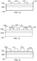
- FIG. 1a, FIG. 1b, FIG. 1c schematic block diagrams of a process of Selective Area Growth (SAG) by Metalorganic Vapor Phase Epitaxy (MOVPE, or also equivalently organometallic vapor-phase epitaxy OMVPE or metalorganic chemical vapor deposition MOCVD) are depicted.
- SAG Selective Area Growth
- MOVPE Metalorganic Vapor Phase Epitaxy
- OMVPE metalorganic chemical vapor deposition MOCVD
- a selective growth of quantum Well on the silicon substrate may be used.
- FIG. 1a depicts a silicon wafer or a Silicon-On-Insulator (SOI) wafer 101 prepared with an oxidation step forming a layer 103.
- a III-V material wafer 105 such as Indium Phosphide (InP) is bonded on the oxidized silicon layer 103 (for example made of silicon dioxide SiO 2 ) through molecular bonding for example.
- the III-V material layer 105 may be thinned by etching to transform it into an III-V material buffer, such as an InP buffer, in the range 10 nm to 5.10 3 nm.
- a dielectric mask 107 for example silicon dioxide SiO 2 is deposited on the InP 105 layer.
- the dielectric mask 107 and the III-V material are representative of the required elements to be present on the monolithically integrated components.
- FIG. 1b depicts the assembly of figure FIG. 1a on which a growth step has been achieved.
- Multiple Quantum Wells (MQW) 109, 111, 113, 115 are grown by a MOVPE method on the InP layer 105, in-between the dielectric mask 107.
- MQW Multiple Quantum Wells
- FIG. 1c depicts the assembly of figure FIG. 1b after removal of the dielectric mask 107. Such removal could be achieved through a chemical process or plasma etching for example.
- the resulting MQW are enabled to form the basis of a light emitting device.
- the MQW 109 forms a laser
- the MQW 111 forms a Multi-Mode Interference (MMI)
- the MQW 113 or 115 form an Electro-Absorption Modulator (EAM).
- MMI Multi-Mode Interference
- EAM Electro-Absorption Modulator
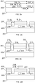
- FIG. 2a, FIG. 2b, FIG. 2c, FIG. 2d schematic block diagrams of steps to combine III-V materials and Silicon materials according to some embodiments are depicted.
- wafer and “layer”, for example in association with a material, such as silicon, silicon-on-insulator, III-V material, are used equivalently hereinafter.
- FIG. 2a depicts a first step in the process of combining Silicon materials and III-V materials according to an embodiment.
- a wafer of Silicon substrate 201 is bonded with an interface layer 203.
- the interface layer 203 is a SiO 2 layer.
- SiO 2 layer 203 may be around 5 nm to 2 ⁇ m of height 203_H.
- a Silicon waveguide 205 is comprised into the interface layer 203.
- the Si waveguide 205 is buried in the interface layer 203, has a height 205_H around 300 nm, and is distant of around 80 nm (205_S) from the top surface of a SiO 2 layer 203.
- Said Si waveguide 205 has a width 205_W of around 700 nm.
- a III-V material layer 207 is bonded to the top surface of the interface layer 203.
- the III-V material layer is an InP layer.
- the bonding may be realized through hydrophilic molecular bonding technique in an example.
- the III-V material layer 207 may be bonded with the appropriate thickness or may be further etched to obtain a thin layer.
- an InP layer 207 has an height 207_H in the range of 50 nm to 1 ⁇ m.
- FIG. 2b depicts a second step in the process of combining Silicon materials and III-V materials according to an embodiment.
- a first recess or trench 209 and a second recess or trench 211 are formed across said layers.
- the first trench 209 defines a substantially vertical recess through the III-V material layer 207 and partly through the interface layer 203.
- the width T_W of a trench is in the magnitude of several micrometers, for example in the range around 1 ⁇ m to around 50 ⁇ m. In an example, the width T_W of the first recess or trench 209 and the second recess or trench 211 is around 10 ⁇ m. In another example the first trench 209 and the second trench 211 have different width in the order of several micrometers.
- the spacing T_D between the first recess 209 and the second recess 211 is between approximately 1 ⁇ m to approximately 100 ⁇ m. In an example the spacing T_D is of around 100 ⁇ m. In an example, several trenches or recesses are formed in the assembly from figure FIG. 2a , the trenches having a spacing periodicity of around 100 ⁇ m. In another example, the spacing between two trenches is lower than 100 ⁇ m, for example inferior to approximately 40 ⁇ m. Such a spacing between two recess is advantageous for growing MQW through selective area growth in an example.
- the first recess or trench 209 and the second recess or trench 211 are symmetrical according to the Si waveguide 205.
- the geometry of the location of the recesses allows an increase in the cooperation between the Si waveguide 205 and the MQW.
- the number of recesses depends on the required number of multiple quantum wells structures to be coupled with the Silicon materials.
- the depth of a recess is sufficient so that the bottom of said recess comprises the interface layer 203.
- a portion of the interface layer 203 is visible through the recess formed in the III-V material layer.
- the depth of the recess is comprised between the height 207_H of the III-V material layer 207 and the height 207_H of said III-V material layer 207 plus the height 203_H of the interface layer 203.
- the recess extends substantially vertically through the III-V material layer 207 sand through a portion of the interface layer 203.
- FIG. 2c depicts another step in the process of combining Silicon materials and III-V materials according to an embodiment.
- the stacked assembly of the Si substrate 201, the SiO 2 layer 203, the Si waveguide 205, the InP layer 207, the first trench 209 and the second trench 211 are exposed to a MOVPE process.
- Multiple Quantum Wells 213, 215, 217 are then grown on the InP layer 207.
- the growth of the MQWs occur on the surface of said InP bonding layer and each MQW 213, 215, 217 is delimited by the respective first trench or recess 209 and second trench or recess 211.
- the dielectric SiO 2 layer 203 acts as a selective mask during the MOVPE process thanks to the presence of the first trench or recess 209 and the second trench or recess 211.
- the thickness of the material deposited in the vicinity of said recesses is related to their respective width T_W.
- the width T_W of a recess is linked to the photoluminescence wavelength emission of said MQW.
- the MQW are grown with a Selective Area Growth method.
- FIG. 2d depicts other steps in the process of combining Silicon materials and III-V materials for obtaining active waveguide structure according to an embodiment.
- Optional steps may be performed on the assembly obtained from figure FIG. 2c in order to design different kind of device.
- the MQW 213 and 217 are removed and MQW 215 is planarized.
- MQW 213 and 217 are replaced by InP buffers 223 and 227.
- An additional InP layer 225 is bonded on top of the MQW 215. It is obtained then an active waveguide structure such as laser or semiconductor optical amplifier (SOA) or a modulator for CWDM transmissions.
- SOA semiconductor optical amplifier
- Multiple quantum well structures have active region, which restricts electron and hole motion in a direction normal to the well, designed for efficient and coherent photon emission.
- the required growth temperature by MOVPE is above 500°C to obtain high quality material.
- Such high temperatures increase the hydrogen desorption from the interface layer.
- the assembly of layers as depicted in FIG. 2c facilitates gas diffusion at the interfaces 219 between the interface layer 203 and the III-V material layer 203. Thanks to the formed first trench or recess 209, during the heating process, a degassing of the hydrogen occurs. A similar degassing phenomenon occur at the interface 221 thanks to the second trench or recess 211.
- FIG. 3a, FIG. 3b, FIG. 3c a schematic block diagram and images of an assembly of III-V materials and Silicon materials are depicted.
- FIG. 3a schematizes a stacked assembly 300 of a Si substrate 301, with an oxidation layer of SiO 2 layer 303, with a InP layer 305 bonded on top of said SiO 2 layer 303, trough molecular bonding for example.
- the stacked assembly 300 is annealed in the same conditions as a MOVPE process.
- the required growth temperature by MOVPE is above 650°C.
- Such high temperatures have an impact on the materials of the stacked assembly 300, and in particular at the interfaces between different type of material.
- the figure FIG. 3b is a microcopy image (100 ⁇ m scale) of a bonded seed or combined material layers of the stacked assembly 300 after annealing.
- Anomalies 313 originates from the instability of the interface layer at high temperature.
- gas is generated at the bonding interface between the interface layer 303 and the III-V material layer 305.
- the gas pierces the III-V material layer 305 resulting in the anomalies 313.
- the figure FIG. 3c is a microscopy image (20 ⁇ m scale) of the same bonded seed.
- the anomalies or imperfections 313 have a relatively high density within the material.
- the anomalies 313 are imperfections or anomalies in the material that decreases the efficiency of the interaction between the different materials. Furthermore, since the density of these anomalies may vary depending on the materials and/or the annealing, more tolerance is induced with regards to the operating points of the stacked assembly 300.
- FIG. 4a, FIG. 4b, FIG. 4c a schematic block diagram and images of an assembly of III-V materials and Silicon materials according to some embodiments are depicted.
- FIG. 4a schematizes a stacked assembly 400 comprising a Si substrate 401, an interface layer 403, a III-V material layer 405, and a first recess 409 extending from the top surface of the III-V material layer 405 down to a portion of the interface layer 403, and a second recess 411 extending from the top surface of the III-V material layer 405 down to a portion of the interface layer 403.
- the first trench or recess 409 and the second trench or recess 411 are separated by approximatively 100 ⁇ m.
- the stacked assembly 400 is obtained according to the steps of the process depict in figures FIG. 2a, 2b .
- the stacked assembly 400 is annealed in the same conditions as a MOVPE process, at more than 600°C.
- FIG. 4b is a microcopy image (100 ⁇ m scale) of a bonded seed of the stacked assembly 400 after annealing.
- the anomalies 413 typically small pockets formed by degassing, have a lower density compared to the anomalies 313 from the stacked assembly 300.
- the InP layer 405 does not exhibit anomalies 413. These areas free from anomalies are extending of a distance L, of approximately 50 ⁇ m from the boundaries of the trenches.
- FIG. 4c is a microscopy image (20 ⁇ m scale) of the stacked assembly 400.
- the InP layer 405 does not exhibit imperfections or anomalies due to the delamination of the InP layer 405 in the surroundings of the trenches.
- trenches allows to avoid generation of anomalies, such as holes or pocked created by degassing, during the heating process of the stacked assembly 400.
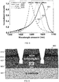
- FIG. 5 a diagram of wavelength emissions according to some embodiments is depicted.
- the figure FIG.5 comprises plots 501, 503, 505 of wavelength emissions obtained from a light emitting device comprising stacked assembly with MQW according to some embodiments.
- the stacked assembly is similar as the assembly 200 from figures FIG. 2a, FIG. 2b, FIG. 2c, FIG. 2d , each stacked assembly comprising a single trench that forms a recess between the III-V material layer and the interface layer.
- the single trench acts as a selective mask for the growth of MQW and as a degassing means and controls the lateral growth of said growth of MQW.
- the plots 501... 505 correspond to wavelength emissions obtained at different point or location on the MQW.
- the x-axis corresponds to wavelengths and has a nm scale.
- the y-axis of the plots 501, 503, 505 corresponds to normalized intensity of the wavelength emissions.
- Table 1 wavelength emissions for different stacked assemblies of Si materials combined with III-V materials Plot reference number Distance to the mask ( ⁇ m) Wavelength of gain maximum (nm) 501 10 1590 503 20 1550 30 1530 40 1515 50 1507 60 1503 70 1500 90 1495 505 120 1490
- the trench or recess acts as a mask that enables to master the growth of MQW, allowing to obtain a span of wavelengths emission by said MQW depending on the distance to the recess.
- Design of various and efficient light emitting device based on stacked assembly of Si materials combined with III-V materials is then facilitated
- a trench allows to avoid creation of anomalies, thanks to a degassing effect, within the materials during heating process, for growing MQW in an example. It is then possible to obtain stacked assemblies of combined Si materials and III-V materials that are more efficient.
- a trench allows also part of the Si materials, such as the SiO 2 layer/substrate to act as a "Selective Area Growth" mask. Therefore, the trench or recess acts as a mask during the growth of MQW. It is then possible to grow MQW with precision and reliability. Furthermore, the process to grow MQW is simplified since a trench or recess is easily formed in the stacked assembly of materials.
- FIG. 6 a schematic block diagram of a photonic device according to some embodiments is depicted.
- a stacked assembly is formed by bonding a III-V material layer 607 on an interface layer 603, which is bonded on a Si substrate 601.
- the interface layer 603 comprises a waveguide 605.
- a recess 609 is formed in the III-V material layer 607 and in the interface layer 603.
- Another recess 611 may also be formed in the stacked assembly.
- An epitaxy growth of Multiple Quantum Well 613 is operated on the stacked assembly.
- Another III-V material layer 615 is bonded on the Multiple Quantum Well 613.
- the stacked assembly 600 forms a photonic device.
- the recess 609 allows to control the growth of the MQW. Thanks to the recess 609, the interface layer 603 and the III-material layer 607 act as a lateral barrier so that the MQW is growing only substantially vertically, and not within the recess 609. According to some embodiments, a trench or recess allows also to avoid lateral overgrowth during the process of MQW growth. Advantageously a thick planar selective area growth is achievable.
- monolithically integrated device for light emission based on an efficient layering of Si material and III-V materials, on which MQW are grown.
- Such monolithically integrated device is particularly adapted for CWDM transmission that require large wavelength distribution.
Landscapes
- Semiconductor Lasers (AREA)
- Optical Integrated Circuits (AREA)
Abstract
Description
- The present invention relates to optical components, in particular to photonic devices.
- Telecommunication architectures and infrastructures are relying more and more on optical communication. Reliable and cost efficient multi gigabit transmissions over optical medium are needed in a broad variety of scenario, such as in datacenters, or for end-user's data delivery. Optical components are thus key components in optical communications to achieve the desired and increasing data rates.
- Silicon-On-Insulator (SOI) waveguide circuits have been in used in the field of optical components. SOI components have a large refractive index which is advantageous for integration and compacity of optical devices. Complementary Metal-Oxide-Semiconductor (CMOS) technology offer the maturity and cost efficiency for advanced photonics components. Combination of III-V materials (combining elements from group III and group V of the periodic table of elements) on top of silicon waveguide circuits allows to design complex integrated circuits by compensating the low efficiency in light emission and amplification of the silicon material. Such combination of different family of materials is achieved with heterogenous integration through wafer bonding.
- An example of heterogenous integration is an optical transceiver based on Distributed Feedback (DFB) lasers with modulation and (de)multiplexing. Such components are used for example for Coarse Wavelength Division Multiplexing (CWDM) transmissions. Compared to Wavelength Division Multiplexing (WDM) or Dense Wavelength Division Multiplexing (DWDM), CWDM resources allocation requires a large channel spacing, usually around 20 nm, in order to be more resilient to variations in temperature and wavelength shifts. Typical CWDM system operates with eight channels/wavelengths in the 1.55 µm region. Laser emissions occur at predefined wavelengths spaced 20 nm apart between 1470 nm and 1610 nm. CWDM lasing components need then to operate on a wavelength distribution of 140 nm which is one of the highest bandgap extensions of active devices.
- DFB laser modules can be hybrid or monolithically integrated. Hybrid laser modules are based on discrete components. Monolithically integrated laser modules simplify alignment and packaging process which is more cost effective. However efficient monolithically integrated DFB are harder to design because of the large required wavelength distribution. An example of a design difficulty is that large lasing wavelength detuning from the gain peak results in Fabry-Pero mode lasing is limiting the number of channels that can be integrated on the same substrate.
- It is then needed to improve optical components with large bandgap regions.
- Example embodiments of the invention aims to remedy all or some of the disadvantages of the above identified prior art.
- The embodiments and features, if any, described in this specification that do not fall under the scope of the independent claims are to be interpreted as examples useful for understanding various embodiments of the invention.
- It is particularly proposed to combine III-V materials with Silicon material.
- A first example embodiment relates then to a method for combining silicon "Si" material and III-V material comprising the following steps:
- layering a Si substrate with an interface layer,
- layering a III-V material layer on the interface layer,
- forming a first recess extending in the III-V material layer and the interface layer.
- Thus, thanks to these features, the method for combining silicon Si material and III-V material offers a recess through the III-V material layer and the interface layer, said recess comprising an interface between said III-V material layer and said interface layer. Advantageously said recess defines a means of interaction between the III-V material layer and the interface layer.
- Another example embodiment relates also to a method for growing Multiple Quantum Well on an assembly of materials comprising the following steps:
- layering a Si substrate with the interface layer,
- layering a III-V material layer on the interface layer,
- forming a first recess extending in the III-V material layer and the interface layer,
- growing Multiple Quantum Well on the III-V material layer,
- wherein the first recess is configured for suppressing an anomaly in the III-V material layer during the step of growing Multiple Quantum Well,
- wherein the first recess is configured for controlling the growth of the Multiple Quantum Well on the III-V material layer.
- Thus, thanks to these features, the method for growing Multiple Quantum Well on an assembly of materials allows the growth of Multiple Quantum Well during which the recess allows to suppress an anomaly in the III-V material layer.
- Advantageously the suppression of the anomaly allows to reach a higher efficiency of the Multiple Quantum Well.
- Advantageously, the recess allows to avoid lateral growth of the Multiple Quantum Well.
- Another example embodiment relates also to a device for combining silicon "Si" material and III-V material comprising:
- a Si substrate,
- an interface layer on the Si substrate,
- a III-V material layer on the interface layer,
- a first recess extending in the III-V material layer and the interface layer,
- said first recess being configured for suppressing an anomaly during heating of the III-V material layer.
- Thus, thanks to these features, the device for combining silicon Si material and III-V material offers a recess through the III-V material layer and the interface layer, said recess comprising an interface between said III-V material layer and said interface layer. Advantageously said recess defines a means of interaction between the III-V material layer and the interface layer.
- Another example embodiment relates also to a photonic device for combining silicon "Si" material and III-V material comprising:
- a Si substrate,
- an interface layer on the Si substrate,
- a waveguide in the interface layer,
- a III-V material layer on the interface layer,
- Multiple Quantum Well on the interface layer, said Multiple Quantum Well being configured to cooperate with the waveguide,
- a first recess extending in the Multiple Quantum Well and in the III-V material layer and the interface layer,
- said first recess being configured for controlling the growth of the Multiple Quantum Well on the III-V material layer.
- said first recess being configured for suppressing an anomaly during heating of the III-V material layer
- Thus, thanks to these features, the photonic device comprises Multiple Quantum Well on the III-V material layer in which anomaly have been removed. The Multiple Quantum Well does not exhibit lateral growth in the recess.
- Advantageously the suppression of the anomaly allows to reach a higher efficiency of the Multiple Quantum Well.
- Advantageously, the recess allows to avoid lateral growth of the Multiple Quantum Well.
- According to various embodiments the method for combining silicon "Si" material and III-V material, the method for growing Multiple Quantum Well on an assembly of materials, the device for combining silicon "Si" material and III-V material, the photonic device for combining silicon "Si" material and III-V material, further comprises respectively one or more of the following features below, which should be considered in any possible technical combinations.
- the first recess is configured for suppressing an anomaly in the III-V material layer during a step of heating the III-V material layer,
- the layering of the III-V material layer on the interface layer is a bonding of the III-V material layer on the interface layer with molecular bonding,
- the interface layer is a dielectric layer,
- the bonding of the III-V material layer on the dielectric layer is an hydrophilic molecular bonding,
- the first recess has a width on the III-V material layer in the range around 1 µm to around 50 µm, preferably around 10 µm,
- a second recess is formed and extends in the III-V material layer and the interface layer,
- the distance on the III-V material layer between the first recess and the second recess is in the range between approximately 1 µm to approximately 100 µm,
- the III-V material layer comprises an Indium Phosphide layer,
- the growing of Multiple Quantum Well on the III-V material layer is a step of Metalorganic Vapor Phase Epitaxy growth of the Multiple Quantum Well,
- the first recess is configured for controlling the growth of the Multiple Quantum Well on the III-V material layer by acting as a growth mask and by avoiding lateral overgrowth of Multiple Quantum Well,
- the first recess is configured for controlling the growth of the Multiple Quantum Well on the III-V material layer by acting as a selective area growth mask.
- Some example embodiments are now described, by way of example only, and with reference to the accompanying drawings in which:
-
FIG. 1a, FIG. 1b, FIG. 1c , are schematic block diagrams depicting steps of a selective area growth by Metalorganic Vapor Epitaxy process, -
FIG. 2a, FIG. 2b, FIG. 2c, FIG. 2d are schematic block diagrams of steps to combine III-V materials and Silicon materials according to some embodiments -
FIG. 3a, FIG. 3b, FIG.3c are schematic block diagram and images of an assembly of III-V materials and Silicon materials, -
FIG. 4a, FIG. 4b, FIG.4c are schematic block diagram and images of an assembly of III-V materials and Silicon materials according to some embodiments, -
FIG. 5 is a diagram of wavelength emissions according to some embodiments, -
FIG. 6 is a schematic block diagram of a photonic device according to some embodiments. - The same reference number represents the same element to the same type of element on all drawings, unless stated otherwise.
- The figures and the following description illustrate specific exemplary embodiments of the invention. It will thus be appreciated that those skilled in the art will be able to devise various arrangements that, although not explicitly described or shown herein, embody the principles of the invention and are included within the scope of the invention. Furthermore, any examples described herein are intended to aid in understanding the principles of the invention, and are to be construed as being without limitation to such specifically recited examples and conditions. As a result, the invention is not limited to the specific embodiments or examples described below, but by the claims and their equivalents.
- In the following description, well-known functions or constructions by the man skilled in the art are not described in detail since they would obscure the invention in unnecessary detail.
- In the following description of the figures, schematic representations are non-limiting and serve only for the understanding of the invention.
- In the following description, the compounds may be written with their respective presence in parenthesis (compound A(d)B(e)C(f) with 'd' mole fraction of 'A', 'e' mole fraction of B and 'f' mole fraction of C) or in indices (same compound AdBeCf with 'd' mole fraction of 'A', 'e' mole fraction of B and 'f' mole fraction of C).
- Referring to figures
FIG. 1a, FIG. 1b, FIG. 1c , schematic block diagrams of a process of Selective Area Growth (SAG) by Metalorganic Vapor Phase Epitaxy (MOVPE, or also equivalently organometallic vapor-phase epitaxy OMVPE or metalorganic chemical vapor deposition MOCVD) are depicted. - For realizing monolithically integrated components enabled to lase at different wavelengths with a large distribution, a selective growth of quantum Well on the silicon substrate may be used.
- Figure
FIG. 1a depicts a silicon wafer or a Silicon-On-Insulator (SOI)wafer 101 prepared with an oxidation step forming alayer 103. A III-V material wafer 105, such as Indium Phosphide (InP) is bonded on the oxidized silicon layer 103 (for example made of silicon dioxide SiO2) through molecular bonding for example. Once an assembly is formed with the III-V material wafer 105 andsilicon wafer 101, the III-V material layer 105 may be thinned by etching to transform it into an III-V material buffer, such as an InP buffer, in the range 10 nm to 5.103 nm. Adielectric mask 107, for example silicon dioxide SiO2 is deposited on theInP 105 layer. Thedielectric mask 107 and the III-V material are representative of the required elements to be present on the monolithically integrated components. - Figure
FIG. 1b depicts the assembly of figureFIG. 1a on which a growth step has been achieved. In an example, Multiple Quantum Wells (MQW) 109, 111, 113, 115 are grown by a MOVPE method on theInP layer 105, in-between thedielectric mask 107. - Figure
FIG. 1c depicts the assembly of figureFIG. 1b after removal of thedielectric mask 107. Such removal could be achieved through a chemical process or plasma etching for example. The resulting MQW are enabled to form the basis of a light emitting device. In an example theMQW 109 forms a laser, theMQW 111 forms a Multi-Mode Interference (MMI) and theMQW - There exist some drawbacks in the process of selective area growth with MOVPE. High temperatures above 500°C are required to the growth of III-V materials. The interfaces between the different materials may suffer from these temperatures, in particular when anomalies are present in the materials or at their interfaces. For example, molecular bonding using hydrophilic direct bonding introduces oxidation of layers with hydrogen production at high temperatures. Such phenomenon can damage the interface layer, lowers the efficiency of the components and renders the process more difficult to achieve.
- Referring to figures
FIG. 2a, FIG. 2b, FIG. 2c, FIG. 2d , schematic block diagrams of steps to combine III-V materials and Silicon materials according to some embodiments are depicted. - The respective terms "wafer" and "layer", for example in association with a material, such as silicon, silicon-on-insulator, III-V material, are used equivalently hereinafter.
- Figure
FIG. 2a depicts a first step in the process of combining Silicon materials and III-V materials according to an embodiment. - A wafer of
Silicon substrate 201 is bonded with aninterface layer 203. In examples theinterface layer 203 is a SiO2 layer. In examples, SiO2 layer 203 may be around 5 nm to 2 µm of height 203_H. - A
Silicon waveguide 205 is comprised into theinterface layer 203. In an example, theSi waveguide 205 is buried in theinterface layer 203, has a height 205_H around 300 nm, and is distant of around 80 nm (205_S) from the top surface of a SiO2 layer 203. SaidSi waveguide 205 has a width 205_W of around 700 nm. - A III-
V material layer 207 is bonded to the top surface of theinterface layer 203. In an example the III-V material layer is an InP layer. The bonding may be realized through hydrophilic molecular bonding technique in an example. The III-V material layer 207 may be bonded with the appropriate thickness or may be further etched to obtain a thin layer. In an example anInP layer 207 has an height 207_H in the range of 50 nm to 1 µm. - In other examples, different configuration of the arrangement of the
Silicon substrate 201, theinterface layer 203, and the III-V material layer 207 are possible. - Figure
FIG. 2b depicts a second step in the process of combining Silicon materials and III-V materials according to an embodiment. - In the stacked layers of
Si substrate 201,interface layer 203,Si waveguide 205 and III-V material layer 207, a first recess ortrench 209 and a second recess ortrench 211 are formed across said layers. Thefirst trench 209 defines a substantially vertical recess through the III-V material layer 207 and partly through theinterface layer 203. The width T_W of a trench is in the magnitude of several micrometers, for example in the range around 1 µm to around 50 µm. In an example, the width T_W of the first recess ortrench 209 and the second recess ortrench 211 is around 10 µm. In another example thefirst trench 209 and thesecond trench 211 have different width in the order of several micrometers. The spacing T_D between thefirst recess 209 and thesecond recess 211 is between approximately 1 µm to approximately 100 µm. In an example the spacing T_D is of around 100 µm. In an example, several trenches or recesses are formed in the assembly from figureFIG. 2a , the trenches having a spacing periodicity of around 100 µm. In another example, the spacing between two trenches is lower than 100 µm, for example inferior to approximately 40 µm. Such a spacing between two recess is advantageous for growing MQW through selective area growth in an example. - In an example, the first recess or
trench 209 and the second recess ortrench 211 are symmetrical according to theSi waveguide 205. Advantageously the geometry of the location of the recesses allows an increase in the cooperation between theSi waveguide 205 and the MQW. - In an embodiment, the number of recesses depends on the required number of multiple quantum wells structures to be coupled with the Silicon materials.
- In an embodiment, the depth of a recess is sufficient so that the bottom of said recess comprises the
interface layer 203. In an example, a portion of theinterface layer 203 is visible through the recess formed in the III-V material layer. In an example the depth of the recess is comprised between the height 207_H of the III-V material layer 207 and the height 207_H of said III-V material layer 207 plus the height 203_H of theinterface layer 203. In an example, the recess extends substantially vertically through the III-V material layer 207 sand through a portion of theinterface layer 203. - Figure
FIG. 2c depicts another step in the process of combining Silicon materials and III-V materials according to an embodiment. - The stacked assembly of the
Si substrate 201, the SiO2 layer 203, theSi waveguide 205, theInP layer 207, thefirst trench 209 and thesecond trench 211 are exposed to a MOVPE process.Multiple Quantum Wells InP layer 207. The growth of the MQWs occur on the surface of said InP bonding layer and eachMQW recess 209 and second trench orrecess 211. - Advantageously, the dielectric SiO2 layer 203 acts as a selective mask during the MOVPE process thanks to the presence of the first trench or
recess 209 and the second trench orrecess 211. The thickness of the material deposited in the vicinity of said recesses is related to their respective width T_W. In case of MQW growth, the width T_W of a recess is linked to the photoluminescence wavelength emission of said MQW. - In an embodiment the MQW are grown with a Selective Area Growth method.
- Figure
FIG. 2d depicts other steps in the process of combining Silicon materials and III-V materials for obtaining active waveguide structure according to an embodiment. - Optional steps may be performed on the assembly obtained from figure
FIG. 2c in order to design different kind of device. In an example theMQW MQW 215 is planarized.MQW InP buffers additional InP layer 225 is bonded on top of theMQW 215. It is obtained then an active waveguide structure such as laser or semiconductor optical amplifier (SOA) or a modulator for CWDM transmissions. - Multiple quantum well structures have active region, which restricts electron and hole motion in a direction normal to the well, designed for efficient and coherent photon emission.
- Referring again to Figure
FIG. 2c , the required growth temperature by MOVPE is above 500°C to obtain high quality material. Such high temperatures increase the hydrogen desorption from the interface layer. Advantageously, the assembly of layers as depicted inFIG. 2c facilitates gas diffusion at theinterfaces 219 between theinterface layer 203 and the III-V material layer 203. Thanks to the formed first trench orrecess 209, during the heating process, a degassing of the hydrogen occurs. A similar degassing phenomenon occur at theinterface 221 thanks to the second trench orrecess 211. - Referring to figures
FIG. 3a, FIG. 3b, FIG. 3c , a schematic block diagram and images of an assembly of III-V materials and Silicon materials are depicted. - The figure
FIG. 3a schematizes astacked assembly 300 of aSi substrate 301, with an oxidation layer of SiO2 layer 303, with aInP layer 305 bonded on top of said SiO2 layer 303, trough molecular bonding for example. - The
stacked assembly 300 is annealed in the same conditions as a MOVPE process. In an example the required growth temperature by MOVPE is above 650°C. Such high temperatures have an impact on the materials of the stackedassembly 300, and in particular at the interfaces between different type of material. - The figure
FIG. 3b is a microcopy image (100 µm scale) of a bonded seed or combined material layers of the stackedassembly 300 after annealing.Anomalies 313 originates from the instability of the interface layer at high temperature. During growth at high temperature, gas is generated at the bonding interface between theinterface layer 303 and the III-V material layer 305. The gas pierces the III-V material layer 305 resulting in theanomalies 313. The figureFIG. 3c is a microscopy image (20 µm scale) of the same bonded seed. The anomalies orimperfections 313 have a relatively high density within the material. - The anomalies 313 (due to degassing of hydrogen bubbles in an example) are imperfections or anomalies in the material that decreases the efficiency of the interaction between the different materials. Furthermore, since the density of these anomalies may vary depending on the materials and/or the annealing, more tolerance is induced with regards to the operating points of the stacked
assembly 300. - Referring to figures
FIG. 4a, FIG. 4b, FIG. 4c , a schematic block diagram and images of an assembly of III-V materials and Silicon materials according to some embodiments are depicted. - The figure
FIG. 4a schematizes astacked assembly 400 comprising aSi substrate 401, aninterface layer 403, a III-V material layer 405, and afirst recess 409 extending from the top surface of the III-V material layer 405 down to a portion of theinterface layer 403, and asecond recess 411 extending from the top surface of the III-V material layer 405 down to a portion of theinterface layer 403. In an example, the first trench orrecess 409 and the second trench orrecess 411 are separated by approximatively 100 µm. - In an example the
stacked assembly 400 is obtained according to the steps of the process depict in figuresFIG. 2a, 2b . - The
stacked assembly 400 is annealed in the same conditions as a MOVPE process, at more than 600°C. - The figure
FIG. 4b is a microcopy image (100 µm scale) of a bonded seed of the stackedassembly 400 after annealing. - The
anomalies 413, typically small pockets formed by degassing, have a lower density compared to theanomalies 313 from the stackedassembly 300. - Around the area of the
trenches interface layer 403, the SiO2 interface layer in an example, at the bottom of the recess of said trenches, theInP layer 405 does not exhibitanomalies 413. These areas free from anomalies are extending of a distance L, of approximately 50 µm from the boundaries of the trenches. - The figure
FIG. 4c is a microscopy image (20 µm scale) of the stackedassembly 400. TheInP layer 405 does not exhibit imperfections or anomalies due to the delamination of theInP layer 405 in the surroundings of the trenches. - Advantageously, the addition of trenches allows to avoid generation of anomalies, such as holes or pocked created by degassing, during the heating process of the stacked
assembly 400. - Referring to
FIG. 5 a diagram of wavelength emissions according to some embodiments is depicted. - The figure
FIG.5 comprisesplots FIG. 2a, FIG. 2b, FIG. 2c, FIG. 2d , each stacked assembly comprising a single trench that forms a recess between the III-V material layer and the interface layer. The single trench acts as a selective mask for the growth of MQW and as a degassing means and controls the lateral growth of said growth of MQW. Theplots 501... 505 correspond to wavelength emissions obtained at different point or location on the MQW. - The x-axis corresponds to wavelengths and has a nm scale. The y-axis of the
plots Table 1: wavelength emissions for different stacked assemblies of Si materials combined with III-V materials Plot reference number Distance to the mask (µm) Wavelength of gain maximum (nm) 501 10 1590 503 20 1550 30 1530 40 1515 50 1507 60 1503 70 1500 90 1495 505 120 1490 - It can be observed that there exists a relationship between the peak wavelength emission from the
plots 501... 505 with their respective distance to the mask. A wavelength shift of around 100 nm occurs between the peak wavelength emission of the wavelength emitted by the MQW from a distance to the recess or mask of 10 µm and the wavelength emitted by said MQW from a distance to the recess or mask of 120 µm. - Advantageously, according to some embodiments, the trench or recess acts as a mask that enables to master the growth of MQW, allowing to obtain a span of wavelengths emission by said MQW depending on the distance to the recess. Design of various and efficient light emitting device based on stacked assembly of Si materials combined with III-V materials is then facilitated
- Furthermore, a trench allows to avoid creation of anomalies, thanks to a degassing effect, within the materials during heating process, for growing MQW in an example. It is then possible to obtain stacked assemblies of combined Si materials and III-V materials that are more efficient.
- According to some embodiments, a trench allows also part of the Si materials, such as the SiO2 layer/substrate to act as a "Selective Area Growth" mask. Therefore, the trench or recess acts as a mask during the growth of MQW. It is then possible to grow MQW with precision and reliability. Furthermore, the process to grow MQW is simplified since a trench or recess is easily formed in the stacked assembly of materials.
- Referring to
FIG. 6 , a schematic block diagram of a photonic device according to some embodiments is depicted. - In an embodiment, a stacked assembly is formed by bonding a III-
V material layer 607 on aninterface layer 603, which is bonded on aSi substrate 601. Theinterface layer 603 comprises awaveguide 605. Arecess 609 is formed in the III-V material layer 607 and in theinterface layer 603. Anotherrecess 611 may also be formed in the stacked assembly. - An epitaxy growth of
Multiple Quantum Well 613 is operated on the stacked assembly. Another III-V material layer 615 is bonded on theMultiple Quantum Well 613. Thestacked assembly 600 forms a photonic device. - The
recess 609 allows to control the growth of the MQW. Thanks to therecess 609, theinterface layer 603 and the III-material layer 607 act as a lateral barrier so that the MQW is growing only substantially vertically, and not within therecess 609. According to some embodiments, a trench or recess allows also to avoid lateral overgrowth during the process of MQW growth. Advantageously a thick planar selective area growth is achievable. - According to some embodiments, it is possible to obtain monolithically integrated device for light emission based on an efficient layering of Si material and III-V materials, on which MQW are grown. Such monolithically integrated device is particularly adapted for CWDM transmission that require large wavelength distribution.
Claims (16)
- A method for combining silicon "Si" material and III-V material comprising the following steps:- layering a Si substrate (201, 401) with an interface layer (203, 403),- layering a III-V material layer (207, 405) on the interface layer (203, 403),- forming a first recess (209, 211) extending in the III-V material layer (207, 405) and the interface layer (203, 403) .
- A method for combining silicon Si material and III-V material according to claim 1, wherein the first recess (209, 211) is configured for suppressing an anomaly (413) in the III-V material layer (207, 405) during a step of heating the III-V material layer (207, 405).
- A method for combining silicon Si material and III-V material according to claim 1 or claim 2, wherein the step of layering the III-V material layer (207, 405) on the interface layer (203, 403) is a step of bonding the III-V material layer (207, 405) on the interface layer (203, 403) with molecular bonding.
- A method for combining silicon Si material and III-V material according to claim 2 and claim 3, further comprising a step of heating of the III-V material layer (207, 405) on the interface layer (203, 403), and wherein the interface layer (203, 403) is a dielectric layer (203, 403).
- A method for combining silicon Si material and III-V material according to any of the claims 1 to claim 4, wherein the interface layer (203, 403) is a dielectric layer (203, 403), and wherein the step of bonding the III-V material layer (207, 405) on the dielectric layer (203, 403) is a step of hydrophilic molecular bonding, and further comprising a step of heating of the III-V material layer (207, 405) on said dielectric layer (203, 403), and wherein the first recess (209, 211) is configured for degassing hydrogen.
- A method for combining silicon Si material and III-V material according to any of the claims 1 to 5, wherein the first recess has a width (T_W) on the III-V material layer (207, 405) in the range around 1 µm to around 50 µm, preferably around 10 µm.
- A method for combining silicon Si material and III-V material according to any of the claims 1 to 6, further comprising a step of forming a second recess (211) extending in the III-V material layer (207, 405) and the interface layer (203, 403), wherein the distance (T_D) on the III-V material layer (207, 405) between the first recess (209) and the second recess (211) is in the range between approximately 1 µm to approximately 100 µm.
- A method for combining silicon Si material and III-V material according to any of the claims 1 to 7, wherein the III-V material layer (207, 405) is an Indium Phosphide layer (207, 405) .
- A method for growing Multiple Quantum Well on an assembly of materials comprising the following steps:- layering a Si substrate (201, 401) with the interface layer (203, 403),- layering a III-V material layer (207, 405) on the interface layer (203),- forming a first recess (209, 211) extending in the III-V material layer (207, 405) and the interface layer (203),- growing Multiple Quantum Well on the III-V material layer (207, 405),- wherein the first recess (209, 211) is configured for suppressing an anomaly (413) in the III-V material layer (207, 405) during the step of growing Multiple Quantum Well,- wherein the first recess (209, 211) is configured for controlling the growth of the Multiple Quantum Well on the III-V material layer (207, 405).
- A method for growing Multiple Quantum Well on an assembly of materials according to claim 9, wherein the step of growing Multiple Quantum Well on the III-V material layer (207, 405) is a step of Metalorganic Vapor Phase Epitaxy growth of the Multiple Quantum Well.
- A method for growing Multiple Quantum Well on an assembly of materials according to claim 9 or claim 10, wherein the first recess (209, 211) is configured for controlling the growth of the Multiple Quantum Well on the III-V material layer (207, 405) by acting as a growth mask and by avoiding lateral overgrowth of Multiple Quantum Well.
- A method for growing Multiple Quantum Well on an assembly of materials according to claim 9 or claim 10, wherein the first recess (209, 211) is configured for controlling the growth of the Multiple Quantum Well on the III-V material layer (207, 405) by acting as a selective area growth mask.
- A method for growing Multiple Quantum Well on an assembly of materials according to any of the claims 9 to claim 12, wherein the interface layer (203, 403) is a dielectric layer (203, 403), and wherein the step of bonding the III-V material layer (207, 405) on the dielectric layer (203, 403) is a step of hydrophilic molecular bonding, and wherein the first recess (209, 211) is configured for degassing hydrogen during the step of growing Multiple Quantum Well on the III-V material layer (207, 405).
- A device for combining silicon "Si" material and III-V material comprising:- a Si substrate (201, 401),- an interface layer (203, 403) on the Si substrate (201, 401),- a III-V material layer (207, 405) on the interface layer (203, 403),- a first recess (209, 211) extending in the III-V material layer (207, 405) and the interface layer (203, 403),- said first recess (209, 211) being configured for suppressing an anomaly (413) during heating of the III-V material layer (207, 405).
- A device for combining silicon "Si" material and III-V material according to claim 13, wherein the interface layer (203, 403) is a dielectric layer and the III-V material layer (207, 405) is an InP layer.
- A photonic device for combining silicon "Si" material and III-V material comprising:- a Si substrate (201, 401),- an interface layer (203, 403) on the Si substrate (201, 401),- a waveguide (205) in the interface layer (203),- a III-V material layer (207, 405) on the interface layer (203, 403),- Multiple Quantum Well on the interface layer (203, 403), said Multiple Quantum Well being configured to be coupled with the waveguide (205),- a first recess (209, 211) extending in the Multiple Quantum Well and in the III-V material layer (207, 405) and the interface layer (203, 403),- said first recess (209, 211) being configured for controlling the growth of the Multiple Quantum Well on the III-V material layer (207, 405).- said first recess (209, 211) being configured for suppressing an anomaly (413) during heating of the III-V material layer (207, 405).
Priority Applications (1)
| Application Number | Priority Date | Filing Date | Title |
|---|---|---|---|
| EP19305873.2A EP3758046B1 (en) | 2019-06-28 | 2019-06-28 | Method for combining silicon material and iii-v material, and associated device |
Applications Claiming Priority (1)
| Application Number | Priority Date | Filing Date | Title |
|---|---|---|---|
| EP19305873.2A EP3758046B1 (en) | 2019-06-28 | 2019-06-28 | Method for combining silicon material and iii-v material, and associated device |
Publications (2)
| Publication Number | Publication Date |
|---|---|
| EP3758046A1 true EP3758046A1 (en) | 2020-12-30 |
| EP3758046B1 EP3758046B1 (en) | 2026-04-15 |
Family
ID=67551494
Family Applications (1)
| Application Number | Title | Priority Date | Filing Date |
|---|---|---|---|
| EP19305873.2A Active EP3758046B1 (en) | 2019-06-28 | 2019-06-28 | Method for combining silicon material and iii-v material, and associated device |
Country Status (1)
| Country | Link |
|---|---|
| EP (1) | EP3758046B1 (en) |
Citations (3)
| Publication number | Priority date | Publication date | Assignee | Title |
|---|---|---|---|---|
| US20070170417A1 (en) * | 2006-01-20 | 2007-07-26 | The Regents Of The University Of California | III-V photonic integration on silicon |
| EP3376525A1 (en) * | 2015-11-12 | 2018-09-19 | Sumco Corporation | Method for manufacturing group iii nitride semiconductor substrate, and group iii nitride semiconductor substrate |
| EP3477717A1 (en) * | 2017-10-25 | 2019-05-01 | Crystalline Mirror Solutions GmbH | Substrate-transferred single-crystal dielectrics for quantum integrated circuits |
Family Cites Families (2)
| Publication number | Priority date | Publication date | Assignee | Title |
|---|---|---|---|---|
| US4910164A (en) * | 1988-07-27 | 1990-03-20 | Texas Instruments Incorporated | Method of making planarized heterostructures using selective epitaxial growth |
| KR102232265B1 (en) * | 2014-07-14 | 2021-03-25 | 주식회사 헥사솔루션 | Substrate structure, method of forming the same and fabricating method for nitride semiconductor using the same |
-
2019
- 2019-06-28 EP EP19305873.2A patent/EP3758046B1/en active Active
Patent Citations (3)
| Publication number | Priority date | Publication date | Assignee | Title |
|---|---|---|---|---|
| US20070170417A1 (en) * | 2006-01-20 | 2007-07-26 | The Regents Of The University Of California | III-V photonic integration on silicon |
| EP3376525A1 (en) * | 2015-11-12 | 2018-09-19 | Sumco Corporation | Method for manufacturing group iii nitride semiconductor substrate, and group iii nitride semiconductor substrate |
| EP3477717A1 (en) * | 2017-10-25 | 2019-05-01 | Crystalline Mirror Solutions GmbH | Substrate-transferred single-crystal dielectrics for quantum integrated circuits |
Also Published As
| Publication number | Publication date |
|---|---|
| EP3758046B1 (en) | 2026-04-15 |
Similar Documents
| Publication | Publication Date | Title |
|---|---|---|
| Fujii et al. | Multiwavelength membrane laser array using selective area growth on directly bonded InP on SiO2/Si | |
| JP5451332B2 (en) | Optical semiconductor device | |
| KR102171268B1 (en) | manufacturing method of Hybrid silicon laser | |
| US11695254B2 (en) | Quantum dot slab-coupled optical waveguide emitters | |
| US20090154517A1 (en) | Hybrid laser diode for single mode operation and method of fabricating the same | |
| CN104769467A (en) | Semiconductor device | |
| CN111580215B (en) | Photonic integrated circuits with improved electrical isolation between N-type contacts | |
| CN111711071B (en) | Tunable laser and method of making the same | |
| JP7046484B2 (en) | Array semiconductor optical elements, optical transmission modules, optical modules, and methods for manufacturing them. | |
| US9372306B1 (en) | Method of achieving acceptable performance in and fabrication of a monolithic photonic integrated circuit (PIC) with integrated arrays of laser sources and modulators employing an extended identical active layer (EIAL) | |
| JP2019054107A (en) | Semiconductor optical device | |
| JP5691741B2 (en) | Optical semiconductor device and manufacturing method thereof | |
| JP2010165759A (en) | Method of manufacturing integrated optical device | |
| WO2019172089A1 (en) | Semiconductor integrated optics element and production method therefor | |
| US20230021415A1 (en) | Manufacturing Method for Semiconductor Device | |
| EP4300850B1 (en) | Modulating amplifier, light-emitting apparatus, optical network unit, and optical line terminal | |
| US7711229B2 (en) | Optical integrated device and manufacturing method thereof | |
| EP3758046B1 (en) | Method for combining silicon material and iii-v material, and associated device | |
| EP2403077B1 (en) | A photonic device and a method of manufacturing a photonic device | |
| US6552358B2 (en) | High power single mode laser and method of fabrication | |
| US20030137023A1 (en) | Optoelectronic device, and method for producing an optoelectronic device | |
| EP4210184A1 (en) | Electro-absorption modulated laser device for flip-chip integration | |
| JP5029239B2 (en) | Semiconductor optical device and manufacturing method thereof | |
| JP2019102581A (en) | Optical semiconductor integrated device, method for manufacturing the same, and optical communication system | |
| US7272161B1 (en) | Epitaxial layer for laser diode ridge protection |
Legal Events
| Date | Code | Title | Description |
|---|---|---|---|
| PUAI | Public reference made under article 153(3) epc to a published international application that has entered the european phase |
Free format text: ORIGINAL CODE: 0009012 |
|
| STAA | Information on the status of an ep patent application or granted ep patent |
Free format text: STATUS: THE APPLICATION HAS BEEN PUBLISHED |
|
| AK | Designated contracting states |
Kind code of ref document: A1 Designated state(s): AL AT BE BG CH CY CZ DE DK EE ES FI FR GB GR HR HU IE IS IT LI LT LU LV MC MK MT NL NO PL PT RO RS SE SI SK SM TR |
|
| AX | Request for extension of the european patent |
Extension state: BA ME |
|
| STAA | Information on the status of an ep patent application or granted ep patent |
Free format text: STATUS: REQUEST FOR EXAMINATION WAS MADE |
|
| 17P | Request for examination filed |
Effective date: 20210630 |
|
| RBV | Designated contracting states (corrected) |
Designated state(s): AL AT BE BG CH CY CZ DE DK EE ES FI FR GB GR HR HU IE IS IT LI LT LU LV MC MK MT NL NO PL PT RO RS SE SI SK SM TR |
|
| RAP3 | Party data changed (applicant data changed or rights of an application transferred) |
Owner name: NOKIA SOLUTIONS AND NETWORKS OY |
|
| STAA | Information on the status of an ep patent application or granted ep patent |
Free format text: STATUS: EXAMINATION IS IN PROGRESS |
|
| 17Q | First examination report despatched |
Effective date: 20250407 |
|
| GRAP | Despatch of communication of intention to grant a patent |
Free format text: ORIGINAL CODE: EPIDOSNIGR1 |
|
| STAA | Information on the status of an ep patent application or granted ep patent |
Free format text: STATUS: GRANT OF PATENT IS INTENDED |
|
| INTG | Intention to grant announced |
Effective date: 20251111 |
|
| GRAS | Grant fee paid |
Free format text: ORIGINAL CODE: EPIDOSNIGR3 |
|
| GRAA | (expected) grant |
Free format text: ORIGINAL CODE: 0009210 |
|
| STAA | Information on the status of an ep patent application or granted ep patent |
Free format text: STATUS: THE PATENT HAS BEEN GRANTED |
|
| AK | Designated contracting states |
Kind code of ref document: B1 Designated state(s): AL AT BE BG CH CY CZ DE DK EE ES FI FR GB GR HR HU IE IS IT LI LT LU LV MC MK MT NL NO PL PT RO RS SE SI SK SM TR |
|
| REG | Reference to a national code |
Ref country code: CH Ref legal event code: F10 Free format text: ST27 STATUS EVENT CODE: U-0-0-F10-F00 (AS PROVIDED BY THE NATIONAL OFFICE) Effective date: 20260415 Ref country code: GB Ref legal event code: FG4D |
|
| REG | Reference to a national code |
Ref country code: DE Ref legal event code: R096 Ref document number: 602019083633 Country of ref document: DE |