EP3758000A1 - Method for programming a phase-change-memory device of a differential type, memory device, and electronic system - Google Patents
Method for programming a phase-change-memory device of a differential type, memory device, and electronic system Download PDFInfo
- Publication number
- EP3758000A1 EP3758000A1 EP20182702.9A EP20182702A EP3758000A1 EP 3758000 A1 EP3758000 A1 EP 3758000A1 EP 20182702 A EP20182702 A EP 20182702A EP 3758000 A1 EP3758000 A1 EP 3758000A1
- Authority
- EP
- European Patent Office
- Prior art keywords
- programming
- current
- memory cells
- drivers
- logic
- Prior art date
- Legal status (The legal status is an assumption and is not a legal conclusion. Google has not performed a legal analysis and makes no representation as to the accuracy of the status listed.)
- Granted
Links
Images



Classifications
-
- G—PHYSICS
- G11—INFORMATION STORAGE
- G11C—STATIC STORES
- G11C13/00—Digital stores characterised by the use of storage elements not covered by groups G11C11/00, G11C23/00, or G11C25/00
- G11C13/0002—Digital stores characterised by the use of storage elements not covered by groups G11C11/00, G11C23/00, or G11C25/00 using resistive RAM [RRAM] elements
- G11C13/0021—Auxiliary circuits
- G11C13/0069—Writing or programming circuits or methods
-
- G—PHYSICS
- G11—INFORMATION STORAGE
- G11C—STATIC STORES
- G11C13/00—Digital stores characterised by the use of storage elements not covered by groups G11C11/00, G11C23/00, or G11C25/00
- G11C13/0002—Digital stores characterised by the use of storage elements not covered by groups G11C11/00, G11C23/00, or G11C25/00 using resistive RAM [RRAM] elements
- G11C13/0004—Digital stores characterised by the use of storage elements not covered by groups G11C11/00, G11C23/00, or G11C25/00 using resistive RAM [RRAM] elements comprising amorphous/crystalline phase transition cells
-
- G—PHYSICS
- G11—INFORMATION STORAGE
- G11C—STATIC STORES
- G11C13/00—Digital stores characterised by the use of storage elements not covered by groups G11C11/00, G11C23/00, or G11C25/00
- G11C13/0002—Digital stores characterised by the use of storage elements not covered by groups G11C11/00, G11C23/00, or G11C25/00 using resistive RAM [RRAM] elements
- G11C13/0021—Auxiliary circuits
- G11C13/0023—Address circuits or decoders
- G11C13/0026—Bit-line or column circuits
-
- G—PHYSICS
- G11—INFORMATION STORAGE
- G11C—STATIC STORES
- G11C13/00—Digital stores characterised by the use of storage elements not covered by groups G11C11/00, G11C23/00, or G11C25/00
- G11C13/0002—Digital stores characterised by the use of storage elements not covered by groups G11C11/00, G11C23/00, or G11C25/00 using resistive RAM [RRAM] elements
- G11C13/0021—Auxiliary circuits
- G11C13/003—Cell access
-
- G—PHYSICS
- G11—INFORMATION STORAGE
- G11C—STATIC STORES
- G11C13/00—Digital stores characterised by the use of storage elements not covered by groups G11C11/00, G11C23/00, or G11C25/00
- G11C13/0002—Digital stores characterised by the use of storage elements not covered by groups G11C11/00, G11C23/00, or G11C25/00 using resistive RAM [RRAM] elements
- G11C13/0021—Auxiliary circuits
- G11C13/0061—Timing circuits or methods
-
- G—PHYSICS
- G11—INFORMATION STORAGE
- G11C—STATIC STORES
- G11C13/00—Digital stores characterised by the use of storage elements not covered by groups G11C11/00, G11C23/00, or G11C25/00
- G11C13/0002—Digital stores characterised by the use of storage elements not covered by groups G11C11/00, G11C23/00, or G11C25/00 using resistive RAM [RRAM] elements
- G11C13/0021—Auxiliary circuits
- G11C13/0097—Erasing, e.g. resetting, circuits or methods
-
- G—PHYSICS
- G11—INFORMATION STORAGE
- G11C—STATIC STORES
- G11C13/00—Digital stores characterised by the use of storage elements not covered by groups G11C11/00, G11C23/00, or G11C25/00
- G11C13/0002—Digital stores characterised by the use of storage elements not covered by groups G11C11/00, G11C23/00, or G11C25/00 using resistive RAM [RRAM] elements
- G11C13/0021—Auxiliary circuits
- G11C13/004—Reading or sensing circuits or methods
-
- G—PHYSICS
- G11—INFORMATION STORAGE
- G11C—STATIC STORES
- G11C13/00—Digital stores characterised by the use of storage elements not covered by groups G11C11/00, G11C23/00, or G11C25/00
- G11C13/0002—Digital stores characterised by the use of storage elements not covered by groups G11C11/00, G11C23/00, or G11C25/00 using resistive RAM [RRAM] elements
- G11C13/0021—Auxiliary circuits
- G11C13/004—Reading or sensing circuits or methods
- G11C2013/0042—Read using differential sensing, e.g. bit line [BL] and bit line bar [BLB]
-
- G—PHYSICS
- G11—INFORMATION STORAGE
- G11C—STATIC STORES
- G11C13/00—Digital stores characterised by the use of storage elements not covered by groups G11C11/00, G11C23/00, or G11C25/00
- G11C13/0002—Digital stores characterised by the use of storage elements not covered by groups G11C11/00, G11C23/00, or G11C25/00 using resistive RAM [RRAM] elements
- G11C13/0021—Auxiliary circuits
- G11C13/0069—Writing or programming circuits or methods
- G11C2013/0078—Write using current through the cell
-
- G—PHYSICS
- G11—INFORMATION STORAGE
- G11C—STATIC STORES
- G11C13/00—Digital stores characterised by the use of storage elements not covered by groups G11C11/00, G11C23/00, or G11C25/00
- G11C13/0002—Digital stores characterised by the use of storage elements not covered by groups G11C11/00, G11C23/00, or G11C25/00 using resistive RAM [RRAM] elements
- G11C13/0021—Auxiliary circuits
- G11C13/0069—Writing or programming circuits or methods
- G11C2013/0088—Write with the simultaneous writing of a plurality of cells
Definitions
- the present invention relates to a method for programming a phase-change-memory device of a differential type, to a phase-change-memory device, and to an electronic system including the phase-change-memory device.
- PCMs non-volatile phase-change memories
- these materials can switch between a disorderly amorphous phase and an orderly crystalline or polycrystalline phase, and the two phases are associated to resistivities of considerably different values, and consequently to different values of a datum stored.
- the elements of Group VI of the Periodic Table such as tellurium (Te), selenium (Se), or antimony (Sb), referred to as chalcogenides or chalcogenic materials, can be advantageously used for providing phase-change-memory cells.
- the phase changes are obtained by locally increasing the temperature of the cells of chalcogenic material, through resistive electrodes (generally known as heaters) arranged in contact with respective regions of chalcogenic material.
- Selection devices for example, MOSFETs
- MOSFETs are connected to the heaters and enable passage of an electric programming current through a respective heater (current pulses known as "SET” and "RESET", which have a respective value, according to the phase change that is to be generated) .
- Said electric current by the Joule effect, generates the temperatures necessary for phase change.
- the state of the chalcogenic material is detected by applying a voltage sufficiently low as not to cause a sensible heating, and then reading the value of the current that flows in the cell. Given that the current is proportional to the conductivity of the chalcogenic material, it is possible to determine in which state the material is, and therefore trace back to the datum stored in the memory cell.
- non-volatile memories comprise an array of memory cells arranged in rows (wordlines) and columns (bitlines). Each memory cell is formed, in the case of PCMs, by a phase-change-memory element and a selector transistor, connected in series.
- a column decoder and a row decoder enable selection, on the basis of address logic signals received at input and using more or less complex decoding schemes, of the memory cells, and in particular of the corresponding wordlines and bitlines each time addressed.
- the column decoder comprises a plurality of analog selection switches (represented by transistors), which receive on their respective control terminals the address signals.
- the selection switches are organised according to a tree structure in hierarchical levels, and their number at each hierarchical level is linked to the organisation and to the size of the memory array.
- the selection switches when enabled, make it possible to bring the bitline selected to a definite voltage and/or current value, according to the operations that are to be implemented.
- a current path is created between a programming stage or a reading stage and the bitline selected. Said current path is defined by the series of a certain number of selection switches.
- sense amplifiers carry out reading of the data stored in the memory cells, comparing the current (or an electrical quantity correlated thereto) that flows in the memory cell selected, also referred to as "direct cell", with a reference current that flows in a complementary cell (implementing the so-called “double-ended reading”).
- the programming step must envisage writing of the logic datum both in the direct memory cell and in the complementary cell.
- the bit written in the complementary cell e.g., logic "0”
- RESET pulse RESET pulse
- each operation of writing of a bit comprises both writing of the direct cells and writing of the corresponding complementary cells to enabling the subsequent reading step.
- This type of memory is known as differential memory.
- the pulses for programming the cells into the SET state and the RESET state have a shape different from one another (therefore, at each pulse the current generator must be configured so as to generate the correct pulse), and at least four sets of pulses, with respective passages of configuration of the current generator, must be envisaged (two for SET/RESET of the direct cells, and two for SET/RESET of the complementary cells).
- This causes a considerable expenditure in terms of time in the programming step and does not allow complete exploitation of the parallelism of the direct cells and of the complementary cells.
- Patent document US2010/182829 refers to semiconductor memories, but does not teach differential writing methods of a PCM memory.
- write amplifiers WA0 and WA1 are designed to write generic bits of an array.
- complementary signals (WD0, /WD0) and (WD1, /WD1) used to pass data solely to write the logical value in a latch; however, differential writing in two associated cells is not discussed.
- the RESET and SET pulses are sent simultaneously, without any relation to the operation of WA0 and WA1.
- the aim of the present invention is to provide a method for programming a phase-change-memory device, and a phase-change-memory device, which will make it possible to solve, either totally or partially, the problems associated to PCM devices of a known type identified above and that will be optimised as regards the operations of programming of the direct and complementary memory cells.
- the aim of the present invention is likewise to provide an electronic system including the phase-change-memory device.
- phase-change-memory device a phase-change-memory device, and an electronic system including the phase-change-memory device are provided, as defined, respectively, in the annexed claims.
- one programming driver dedicated to writing of the direct cells Activation of one programming driver or the other depends upon the datum that is to be written (logic datum "0”, or RESET; logic datum "1", or SET)
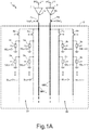
- FIG. 1A Illustrated schematically, and designated as a whole by the reference number 1 in Figure 1A is a portion of a non-volatile memory device, in particular of a PCM type, limitedly to just the parts necessary for an understanding of the present invention.
- the memory device 1 comprises: a programming driver 7 having an output 7a connected to a main bitline MBL D ' via a respective selector 4a (here, by way of example, a MOSFET of a p-MOS type); and a programming driver 9 having an output 9a connected to a main bitline MEL C ' via a respective selector 5a (here, by way of example, a MOSFET of a p-MOS type).
- the programming drivers 7 and 9 form a programming stage of the memory device 1.
- the memory device 1 further comprises a memory array 2, including a plurality of first memory cells 3a and a plurality of second memory cells 3b, which can be selected by respective local wordlines WL ⁇ 0>, WL ⁇ 1>, ... and local bitlines BL ⁇ 0>, ..., BL ⁇ 7>.
- the wordlines corresponding to the portion of the direct cells are identified by the subscript "D" (WL D ⁇ >), whereas the wordlines corresponding to the portion of the complementary cells are identified by the subscript "C" (WL C ⁇ >); the same applied to the bitlines.
- the second memory cells 3b correspond, as regards number and manufacturing characteristics, to the first memory cells 3a.
- the second memory cells 3b store a logic datum complementary to that of the first memory cells 3a.
- the second memory cells 3b are queried during double-ended reading of the first memory cells 3a in order to read the logic datum stored in the first memory cells 3a via comparison with the logic datum stored in respective second memory cells 3b.
- the first memory cells 3a form a first memory portion 2a'; the second memory cells 3b form a second memory portion 2b' .
- the local bitlines BL ⁇ 0> - BL ⁇ 7> of the first memory portion 2a' are connected to the main bitline MBL D '.
- the local bitlines BL ⁇ 0> - BL ⁇ 7> of the second memory portion 2b' are connected to the main bitline MBL C '.
- the memory cells 3a, 3b are identical to one another and comprise a phase-change element and a selector element, operatively coupled thereto (not illustrated in detail).
- the phase-change element includes a phase-change material (for example, a chalcogenide) and is therefore able to store data in the form of levels of resistance associated to the different phases assumed by the phase-change material (therefore it operates like a resistor with variable resistance).
- the selector element is, for example, a MOS transistor having its gate terminal connected to the respective wordline WL ⁇ 0>, WL ⁇ 1>, ..., a first conduction terminal connected to the phase-change element, and a second conduction terminal connected to a reference potential (for example, ground).
- the selector element is controlled so as to enable, when selected (i.e., switched on via the signal of the respective local wordline WL ⁇ 0>, WL ⁇ 1>, ..., to which it is coupled), passage of a writing/reading current through the phase-change element during the respective operation of writing/reading of a logic datum in said phase-change element.
- the non-volatile memory device 1 further comprises a row decoder (here not illustrated), adapted to select the local wordline WL ⁇ 0>, WL ⁇ 1>, ..., corresponding to the memory cell 3a, 3b each time to be addressed, and a column decoder (here not illustrated), adapted to select the bitline of the memory cell 3a, 3b to be addressed.
- a row decoder here not illustrated
- a column decoder here not illustrated
- a reading stage of a type in itself known and including a sense amplifier (not illustrated), has inputs coupled to the main bitlines MBL D ' and MBL C ' via the switches 4a and 5a, respectively.
- the switches 4a, 5a are driven in conduction and inhibition according to the need to access the respective main bitline MBL D ', MBL C ', for programming of the memory cells 3a, 3b connected thereto.
- the programming drivers 7 and 9 are implemented by a current mirror and receive at input a respective current signal PG IN_D [i] and PG IN_C [i], which represents both the logic datum to be written ("1" or "0") and the signal of switching-on or activation of the respective programming driver 7 and 9 to enable passage of the current signal PG IN_D [i] and PG IN_C [i]. In this way, it is the datum to be written itself that enables the respective programming driver 7 or 9.
- the selectors 4a and 5a receive on their respective control terminals switching-on/switching-off signals YNP D and YNP C , respectively.
- Further selection switches 8a, 8b (of a p-MOS type) are provided, in a per se known manner, for selecting/deselecting the bitlines BL ⁇ 0> - BL ⁇ 7> of the first and second memory portions 2a', 2b'.
- the selection switches are organised according to a tree structure in hierarchical levels, and their number in each hierarchical level is linked to the organisation and to the size of the memory array.
- the selectors 4a, 5a once enabled, make it possible to bring the bitline selected to a definite voltage and/or current value according to the operations that are to be implemented; in particular, a current path is created between the programming stage and the bitline selected.
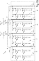
- Figure 1B illustrates two programming drivers 7, 9 each coupled to a respective plurality of main bitlines MBL D ', MBL D ", and MBL C ', MBL C ". Connected to each main bitline are local bitlines and memory cells, as already described and illustrated with reference to Figure 1A .
- a memory device 1' moreover includes: a third main bitline MBL D " coupled, via a respective MOSFET selector 4b (of a p-MOS type), to the programming driver 7; and a fourth main bitline MBL C " coupled, via a respective MOSFET selector 5b, to the programming driver 9.
- Coupled to the third main bitline MBL D " are local bitlines BL ⁇ 0> - BL ⁇ 7>, and coupled to each local bitline BL ⁇ 0> - BL ⁇ 7> are memory cells 6a to form a memory portion 2a" that repeats the circuit diagram already described with reference to the memory portion 2a' of Figure 1A .
- coupled to the fourth main bitline MBL C " are local bitlines BL ⁇ 0> - BL ⁇ 7>, and coupled to each local bitline BL ⁇ 0> - BL ⁇ 7> are memory cells 6b to form a memory portion 2b" that repeats the circuit diagram already described with reference to the memory portion 2b' of Figure 1A .
- the present invention likewise applies to a memory in which the circuit diagram of Figure 1A or Figure 1B repeats for a number N of times (where N is comprised, for example, between 40 and 128), therefore including a number of programming drivers equal to 2N.
- Figure 1 illustrates in fact an i-th circuit diagram of the N circuit diagrams that may be present and that, typically, are present in a memory of large dimensions.
- the present invention envisages that programming of the memory cells 3a, 3b is carried out according to the timing chart illustrated in Figure 2 .
- programming of the memory cells takes place by words of bits, i.e., by selecting and writing an entire wordline WL ⁇ 0> or WL ⁇ 1>, etc., of the memory array 2. What is described hereinafter consequently applies to writing of a word in a respective wordline, for example a word in the wordline WL ⁇ 0>.
- a RESET pulse is generated, i.e., an electrical pulse adapted to program the memory cells 3a, 3b addressed by the wordline WL ⁇ 0> into the logic state "0".
- this interval T1 all the direct and complementary cells that, in the wordline WL ⁇ 0>, are to be programmed with the RESET pulse are simultaneously programmed.
- all and only the programming drivers if the memory 1 that are coupled to memory cells 3a, 3b to be programmed with the RESET pulse are activated.
- the programming driver 7 is operatively coupled (via the respective main bitline MBL D ' and local bitline BL) to a memory cell 3a to be programmed, the programming driver 7 is activated (i.e., the programming current flows through the respective programming driver and main bitline to reach the memory cell 3a to be programmed).
- the RESET pulse is transmitted only through the active programming drivers.
- all the programming drivers that are not operatively coupled to memory cells that are to be programmed with the RESET pulse are deactivated.
- the memory cells 3a, 3b that are to be programmed are addressed by appropriately selecting the corresponding wordline WL and the corresponding bitline BL, in a per se known manner and corresponding to the prior art. There is thus obtained the desired programming for all and only the memory cells 3a, 3b that are to be programmed with the RESET pulse, irrespective of whether they are cells of a direct type or of a complementary type. Given that the datum is differential (if the direct cell is in the SET state, the complementary cell is in the RESET state, and vice versa) the maximum parallelism is always exploited because, whatever the datum, there will be a number of cells equal to the number of bits in the word, and likewise a number of cells to be set equal to the number of bits in the word.
- a SET pulse is generated for programming the remaining memory cells belonging to the same wordline WL ⁇ 0> previously selected.
- all the direct and complementary cells that are to be programmed with the SET pulse are simultaneously programmed.
- all and only the programming drivers coupled to main bitlines that are in turn coupled to memory cells to be programmed with the SET pulse are activated.
- the programming driver 7 is operatively coupled (via the respective main bitline MBL D ') to a cell 3a to be programmed with the SET pulse, this programming driver 7 is activated (i.e., the programming current flows through the respective programming driver and main bitline to reach the memory cell).
- the SET pulse is transmitted only through the active programming drivers. At the same time, all the programming drivers that are not operatively coupled to memory cells that are to be programmed with the SET pulse are deactivated.
- the memory cells 3a, 3b that are to be programmed are addressed by appropriately selecting the corresponding wordline WL and corresponding bitline BL, in a per se known manner and in line with the prior art. There is thus obtained the desired programming for all and only the memory cells 3a, 3b that are to be programmed with the SET pulse, irrespective of whether they are cells of a direct type or of a complementary type.
- All the cells corresponding the word that is being written in the corresponding wordline WL ⁇ 0> of the memory 2 i.e., both the direct cells and the complementary cells
- interval T1 can be used for generating the SET pulse, and the interval T2 for generating the RESET pulse.
- the logic circuit 30 comprises a multiplexer 32 having two signal inputs 32a, 32b, a control input 32c, and an output 32d.
- the control input 32c receives a digital control signal SET_P that assumes the digital values "0" or “1”, where "0” controls the multiplexer 32 so as to transfer onto the output 32d the logic datum DATA_IN[i] at the input 32a (corresponding to the negated value of DATA_IN[i]), and "1" controls the multiplexer 32 so as to transfer onto the output 32d the logic datum DATA_IN[i] at the input 32b.
- the logic circuit 30 further comprises a first NAND logic gate 34, having an input 34a that is connected to the output 32d of the multiplexer 32 (and receives the logic signal DATA_DIR[i]), and an input 34b configured to receive an enable signal EN_PL_PULSE that assumes the digital values "0" or "1".
- the logic circuit 30 further comprises a second NAND logic gate 36, having an input 36a that is connected to the output 32d of the multiplexer 32 (and receives the logic signal DATA_COMP[i]), and an input 36b configured to receive the enable signal EN_PL_PULSE.
- the output from the NAND gate 34 is the signal ENAB_D[i] that represents the (low-voltage) enable signal for the programming driver corresponding to the direct cell of the i-th bit.
- the output from the NAND gate 36 is the signal ENAB_C[i] and likewise represents the (low-voltage) enable signal for the programming driver corresponding to the complementary cell of the i-th bit.
- the logic circuit 30 further comprises a first level shifter 37 and a second level shifter 41, which are coupled, respectively, to the output of the NAND gate 34 and to the output of the NAND gate 36, for receiving the signal ENAB_D[i] and the signal ENAB_C[i], respectively.
- the first and second level shifters 37, 41 have the function of shifting the signals from the value managed by the logic gates (typically, a value V DD12 of 1.2V ⁇ 10%) to a higher value (typically, a value V HIGH ranging between 4.5 and 6 V) .
- the logic circuit 30 further comprises a buffer 38 and a buffer 39, which have the function of inverting the signal, given that the programming driver is of a P type (i.e., closed if it is driven by a "0"), thus generating the current signals PG IN_D [i] and PG IN_C [i] for controlling the capacitive load.
- the negated logic bit of DATA_IN[i] will be transferred to the output 32d of the multiplexer 32; in the case where it is T2, the logic bit of DATA_IN[i] will be transferred to the output 32d of the multiplexer 32.
- the number of logic circuits 30, of the type illustrated in Figure 3 is equal to the maximum length of a digital word that can be stored in the memory 2.
- Each logic circuit 30, in fact, receives a respective (i-th) bit of DATA_IN[i] and generates two outputs that are adapted to form the input of respective programming drivers 7, 9 and to control activation and switching-off of the respective programming drivers 7, 9 in order to write a logic datum and its complementary in the respective memory cells addressed.
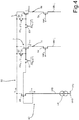
- FIG. 4 illustrates a circuit implementation of the drivers 7, 9, which are activated according to the logic datum to be written.
- the circuit of Figure 4 comprises a main branch, or control branch, 42, which includes: a current generator 44, configured to co-operate in the generation of a RESET pulse or SET pulse, according to the operating condition, which is connected between a reference terminal 44a (ground) and a biasing terminal 44b; and a first current-mirror device 48 (here, a diode-connected MOSFET of a P type), forming a first element of a current mirror 50.
- a current generator 44 configured to co-operate in the generation of a RESET pulse or SET pulse, according to the operating condition, which is connected between a reference terminal 44a (ground) and a biasing terminal 44b
- a first current-mirror device 48 here, a diode-connected MOSFET of a P type
- the current generator 44 and the first current-mirror device 48 are connected together in series between the reference ground terminal 44a and a line at the potential V HIGH , for example equal to 5 V, to form the control branch 42.
- a current i CTR flows between the line at the potential V HIGH and the reference ground terminal 44a.
- the current i CTR which flows through the control branch 42, is mirrored, through the current mirror 50, in respective programming currents I PROG of a plurality of main bitlines MBL D ', MBL C ', etc. (i.e., all the main bitlines that form part of the memory device 1).
- the current I PROG (RESET or SET pulse, according to the operating condition, as mentioned previously) flows through the respective main bitline MBL D ', MBL C ', ..., according to the activation of further respective current-mirror devices 56, 57 (here, P-type MOSFETs) connected in current-mirror configuration to the first current-mirror device 48.
- activation of the further current-mirror devices 56, 57 is controlled by two respective switches, which are, in turn, switched-on/switched-off by the signals generated at output from the logic circuit 30 of Figure 3 (i.e., the signals PG IN_D [i] and PG IN_C [i]).
- a switch 61 e.g., a P-channel transistor
- a switch 62 e.g., a P-channel transistor
- the current i CTR on the control branch 42 is mirrored in the main bitline MBL D ' when the switch 61 is on and the switch 62 is off, i.e., only when the control signal applied to the respective gate terminal (/PG IN_D [i] and PG IN_D [i]) has a value such as to bring the switch 61 into an operating state of current conduction and the switch 62 into an operating state of inhibition (here, the signal PG IN_D [i] applied to the switch 62 is complementary to the signal /PG IN_D [i] applied to the switch 61).
- the switch 61 is open and the switch 62 is closed, under the control of the signals /PG IN_D [i] and PG IN_D [i].
- a switch 63 coupled between the gate of the current-mirror device 57 and the gate of the current-mirror device 48; and a switch 64, coupled between the gate of the current-mirror device 57 and the line at the potential V HIGH .
- the current i CTR on the control branch 42 is effectively mirrored in the main bitline MBL C ' only when the switch 63 is on and the switch 64 is off, i.e., only when the respective control signals /PG IN_C [i] and PG IN_C [i] applied on their respective gate terminals have a value such as to bring the switch 63 into an operating state of current conduction and the switch 64 into an operating state of inhibition (here, the signal PG IN_C [i] applied to the switch 64 is complementary to the signal /PG IN_C [i] applied to the switch 63).
- the switch 63 is open and the switch 64 is closed, under the control of the signals /PG IN_C [i] and PG IN_C [i].
- FIG. 6 illustrates a portion of an electronic system 100, according to a further embodiment of the present invention.
- the electronic system 100 can be used in electronic devices, such as: a PDA (Personal Digital Assistant); a portable or fixed computer, possibly with wireless data-transfer capacity; a mobile phone; a digital audio player; a photographic or video camera; or further devices capable of processing, storing, transmitting, and receiving information.
- PDA Personal Digital Assistant
- the electronic system 100 comprises: a controller 101 (for example, provided with a microprocessor, a DSP, or a microcontroller); an input/output device 102 (for example, provided with a keypad and a display), for entering and displaying data; the non-volatile memory device 1 or 1', provided with the array of memory cell of the phase-change type, previously described; a wireless interface 104, for example an antenna, for transmitting and receiving data through a radiofrequency wireless communications network; and a RAM 105, all coupled through a bus 106.
- a battery 107 can be used as electrical power-supply source in the electronic system 100, which can moreover be provided with a photographic or video camera 108.
- the array is written in a differential way and therefore the write amplifiers (program drivers) are doubled with respect to those that actually generate the pulse; on this assumption, two groups of program drivers are designed that are alternatively activated and distributed between the cells to be reset and cells to be set.
- the RESET and SET pulses are powered following two separate phases (see Figure 2 ), since the structure is designed in such a way that half of the cells receive the RESET pulse and half of the cells receive the SET pulse. These are therefore two separate and balanced events per number of cells, with two groups of dedicated program loads (PG IN_D and PG IN_C ).
- the programming (writing) time of the memory is considerably reduced, in so far as an entire digital word (both in the direct form and in the complementary form) is written in just two time intervals.
- the programming-control part is simplified, in so far as it is not necessary to preselect the type of bits to be written and therefore the corresponding current pulse (SET/RESET) to be generated.
- Figure 5 shows a logic circuit 30' that comprises, in addition to the elements already described with reference to Figure 3 , further AND logic gates 72, 74 (optional) arranged between the output of the multiplexer 32 and, respectively, the input 34a of the logic gate 34 and the input 36a of the logic gate 36.
- the AND logic gate 72 has three inputs 72a-72c and one output 72d.
- An input 72a is coupled to the output 32d of the multiplexer 32, whereas the other inputs 72b and 72c receive respective signals MODIFY_DIR[i] and MASK_PAR[i].
- the signal MASK_PAR[i] is a logic datum "1" or "0" and indicates the writing parallelism (in fact, in a per se known manner, not always is it possible to manage to program simultaneously a number of bits equal to that of the word, on account of constraints of maximum current that can be delivered).
- the output 72d of the AND logic gate 72 generates the signal DATA_DIR[i] supplied to the input 34a of the logic gate 34.
- the AND logic gate 74 has three inputs 74a-74c and one output 74d.
- An input 74a is coupled to the output 32d of the multiplexer 32 via an inverter (in order to receive the negated logic datum), while the other inputs 74b and 74c receive respective signals MODIFY_COMP[i] and MASK_PAR[i].
- the signal MODIFY_COMP[i] has a function analogous to that of the signal MODIFY_DIR[i]. The same applies to the signal MASK_PAR[i].
- the output 74d of the AND logic gate 74 generates the signal DATA_COMP[i] supplied to the input 36a of the logic gate 36.
Landscapes
- Chemical & Material Sciences (AREA)
- Crystallography & Structural Chemistry (AREA)
- Read Only Memory (AREA)
- Semiconductor Memories (AREA)
Abstract
Description
- The present invention relates to a method for programming a phase-change-memory device of a differential type, to a phase-change-memory device, and to an electronic system including the phase-change-memory device.
- Known to the art are non-volatile phase-change memories (PCMs), in which, for storing information, the characteristics of materials that have the property of switching between phases that have different electrical characteristics are exploited. For instance, these materials can switch between a disorderly amorphous phase and an orderly crystalline or polycrystalline phase, and the two phases are associated to resistivities of considerably different values, and consequently to different values of a datum stored. For instance, the elements of Group VI of the Periodic Table, such as tellurium (Te), selenium (Se), or antimony (Sb), referred to as chalcogenides or chalcogenic materials, can be advantageously used for providing phase-change-memory cells. The phase changes are obtained by locally increasing the temperature of the cells of chalcogenic material, through resistive electrodes (generally known as heaters) arranged in contact with respective regions of chalcogenic material. Selection devices (for example, MOSFETs), are connected to the heaters and enable passage of an electric programming current through a respective heater (current pulses known as "SET" and "RESET", which have a respective value, according to the phase change that is to be generated) . Said electric current, by the Joule effect, generates the temperatures necessary for phase change. During reading, the state of the chalcogenic material is detected by applying a voltage sufficiently low as not to cause a sensible heating, and then reading the value of the current that flows in the cell. Given that the current is proportional to the conductivity of the chalcogenic material, it is possible to determine in which state the material is, and therefore trace back to the datum stored in the memory cell.
- In a known way, non-volatile memories comprise an array of memory cells arranged in rows (wordlines) and columns (bitlines). Each memory cell is formed, in the case of PCMs, by a phase-change-memory element and a selector transistor, connected in series. A column decoder and a row decoder enable selection, on the basis of address logic signals received at input and using more or less complex decoding schemes, of the memory cells, and in particular of the corresponding wordlines and bitlines each time addressed.
- The column decoder comprises a plurality of analog selection switches (represented by transistors), which receive on their respective control terminals the address signals. The selection switches are organised according to a tree structure in hierarchical levels, and their number at each hierarchical level is linked to the organisation and to the size of the memory array. The selection switches, when enabled, make it possible to bring the bitline selected to a definite voltage and/or current value, according to the operations that are to be implemented. In particular, a current path is created between a programming stage or a reading stage and the bitline selected. Said current path is defined by the series of a certain number of selection switches.
- In a known way, sense amplifiers carry out reading of the data stored in the memory cells, comparing the current (or an electrical quantity correlated thereto) that flows in the memory cell selected, also referred to as "direct cell", with a reference current that flows in a complementary cell (implementing the so-called "double-ended reading"). Obviously, also the programming step must envisage writing of the logic datum both in the direct memory cell and in the complementary cell. For instance, the bit written in the complementary cell (e.g., logic "0") is associated to a RESET state, or RESET pulse, whereas the same bit (e.g., logic "0") is written in the direct cell by a SET pulse. Therefore, each operation of writing of a bit comprises both writing of the direct cells and writing of the corresponding complementary cells to enabling the subsequent reading step. This type of memory is known as differential memory.
- In order to speed up the programming (writing) operations, it is known to write a number of bits in parallel by programming in parallel memory cells according to the type of pulse (RESET or SET) to be sent and according to the type of cell (whether direct or complementary). For instance, the direct cells are accessed, and the ones that are to be programmed with the datum "0" are programmed simultaneously with said datum; then, maintaining access to the direct cells active, the ones that are to be programmed with the datum "1" are programmed simultaneously with said datum. The same procedure is carried out for the complementary cells.
- It is evident that this type of approach presents some disadvantages.
- In particular, the pulses for programming the cells into the SET state and the RESET state, respectively, have a shape different from one another (therefore, at each pulse the current generator must be configured so as to generate the correct pulse), and at least four sets of pulses, with respective passages of configuration of the current generator, must be envisaged (two for SET/RESET of the direct cells, and two for SET/RESET of the complementary cells). This causes a considerable expenditure in terms of time in the programming step and does not allow complete exploitation of the parallelism of the direct cells and of the complementary cells.
- The patent document
US2018/108405 refers to the reading path and in particular describes the decoding in the case of differential and single ended reading. - Patent document
US2010/182829 refers to semiconductor memories, but does not teach differential writing methods of a PCM memory. In this document, write amplifiers WA0 and WA1 are designed to write generic bits of an array. There are cited complementary signals (WD0, /WD0) and (WD1, /WD1) used to pass data solely to write the logical value in a latch; however, differential writing in two associated cells is not discussed. As shown in Figure 8 ofUS2010/182829 , the RESET and SET pulses are sent simultaneously, without any relation to the operation of WA0 and WA1. - The aim of the present invention is to provide a method for programming a phase-change-memory device, and a phase-change-memory device, which will make it possible to solve, either totally or partially, the problems associated to PCM devices of a known type identified above and that will be optimised as regards the operations of programming of the direct and complementary memory cells. The aim of the present invention is likewise to provide an electronic system including the phase-change-memory device.
- Consequently, according to the present invention a method for programming a phase-change-memory device, a phase-change-memory device, and an electronic system including the phase-change-memory device are provided, as defined, respectively, in the annexed claims.
- For a better understanding of the present invention, preferred embodiments thereof are now described, purely by way of non-limiting example and with reference to the attached drawings, wherein:
-
Figures 1A and1B show respective circuits for programming a non-volatile memory device, in particular of a PCM type, according to an embodiment of the present invention and limitedly to portions of the non-volatile memory device of interest for an understanding of the present invention; -
Figure 2 illustrates a timing chart corresponding to writing of a logic word in the non-volatile memory device ofFigures 1A and1B , according to one aspect of the present invention; -
Figure 3 illustrates a logic circuit for generating programming pulses for direct cells and respective complementary cells as a function of a bit of the logic word to be written; -
Figure 4 illustrates a simplified circuit implementation of programming drivers for direct and complementary memory cells; -
Figure 5 illustrates a logic circuit for generating programming pulses for direct cells and respective complementary cells as a function of a bit of the logic word to be written, according to a further embodiment with respect to that ofFigure 3 ; and -
Figure 6 is a simplified block diagram of an electronic system incorporating the non-volatile memory device, in an embodiment of the present invention. - According to the present invention, it is proposed to use two programming drivers for programming the memory cells, i.e., one programming driver dedicated to writing of the direct cells and one programming driver dedicated to writing of the complementary cells. Activation of one programming driver or the other depends upon the datum that is to be written (logic datum "0", or RESET; logic datum "1", or SET)
- Illustrated schematically, and designated as a whole by the
reference number 1 inFigure 1A is a portion of a non-volatile memory device, in particular of a PCM type, limitedly to just the parts necessary for an understanding of the present invention. - In particular, the
memory device 1 comprises: aprogramming driver 7 having anoutput 7a connected to a main bitline MBLD' via arespective selector 4a (here, by way of example, a MOSFET of a p-MOS type); and aprogramming driver 9 having anoutput 9a connected to a main bitline MELC' via arespective selector 5a (here, by way of example, a MOSFET of a p-MOS type). Theprogramming drivers memory device 1. - The
memory device 1 further comprises amemory array 2, including a plurality offirst memory cells 3a and a plurality ofsecond memory cells 3b, which can be selected by respective local wordlines WL<0>, WL<1>, ... and local bitlines BL<0>, ..., BL<7>. InFigure 1 , the wordlines corresponding to the portion of the direct cells are identified by the subscript "D" (WLD<>), whereas the wordlines corresponding to the portion of the complementary cells are identified by the subscript "C" (WLC<>); the same applied to the bitlines. In a per se known manner, thesecond memory cells 3b correspond, as regards number and manufacturing characteristics, to thefirst memory cells 3a. In use, thesecond memory cells 3b store a logic datum complementary to that of thefirst memory cells 3a. Thesecond memory cells 3b are queried during double-ended reading of thefirst memory cells 3a in order to read the logic datum stored in thefirst memory cells 3a via comparison with the logic datum stored in respectivesecond memory cells 3b. - The
first memory cells 3a form afirst memory portion 2a'; thesecond memory cells 3b form asecond memory portion 2b' . - The local bitlines BL<0> - BL<7> of the
first memory portion 2a' are connected to the main bitline MBLD'. The local bitlines BL<0> - BL<7> of thesecond memory portion 2b' are connected to the main bitline MBLC'. - The
memory cells - The
non-volatile memory device 1 further comprises a row decoder (here not illustrated), adapted to select the local wordline WL<0>, WL<1>, ..., corresponding to thememory cell memory cell memory cell - A reading stage, of a type in itself known and including a sense amplifier (not illustrated), has inputs coupled to the main bitlines MBLD' and MBLC' via the
switches - During writing, the
switches memory cells - According to an aspect of the present invention, the
programming drivers respective programming driver respective programming driver - The
selectors Further selection switches second memory portions 2a', 2b'. In general, the selection switches are organised according to a tree structure in hierarchical levels, and their number in each hierarchical level is linked to the organisation and to the size of the memory array. Like theselection switches selectors -
Figure 1B illustrates twoprogramming drivers Figure 1A . In addition to what has already been described with reference toFigure 1A , inFigure 1B a memory device 1' moreover includes: a third main bitline MBLD" coupled, via arespective MOSFET selector 4b (of a p-MOS type), to theprogramming driver 7; and a fourth main bitline MBLC" coupled, via a respective MOSFET selector 5b, to theprogramming driver 9. - Coupled to the third main bitline MBLD" are local bitlines BL<0> - BL<7>, and coupled to each local bitline BL<0> - BL<7> are
memory cells 6a to form amemory portion 2a" that repeats the circuit diagram already described with reference to thememory portion 2a' ofFigure 1A . Likewise, coupled to the fourth main bitline MBLC" are local bitlines BL<0> - BL<7>, and coupled to each local bitline BL<0> - BL<7> arememory cells 6b to form amemory portion 2b" that repeats the circuit diagram already described with reference to thememory portion 2b' ofFigure 1A . - Moreover, it may be noted that the present invention likewise applies to a memory in which the circuit diagram of
Figure 1A orFigure 1B repeats for a number N of times (where N is comprised, for example, between 40 and 128), therefore including a number of programming drivers equal to 2N.Figure 1 illustrates in fact an i-th circuit diagram of the N circuit diagrams that may be present and that, typically, are present in a memory of large dimensions. - In the sequel of the description, reference will be made to
Figure 1A , without this implying any loss of generality. - The present invention envisages that programming of the
memory cells Figure 2 . - According to an embodiment, programming of the memory cells takes place by words of bits, i.e., by selecting and writing an entire wordline WL<0> or WL<1>, etc., of the
memory array 2. What is described hereinafter consequently applies to writing of a word in a respective wordline, for example a word in the wordline WL<0>. - With reference to
Figure 2 , in a time interval T1, a RESET pulse is generated, i.e., an electrical pulse adapted to program thememory cells memory 1 that are coupled tomemory cells programming driver 7 is operatively coupled (via the respective main bitline MBLD' and local bitline BL) to amemory cell 3a to be programmed, theprogramming driver 7 is activated (i.e., the programming current flows through the respective programming driver and main bitline to reach thememory cell 3a to be programmed). - In this way, the RESET pulse is transmitted only through the active programming drivers. At the same time, all the programming drivers that are not operatively coupled to memory cells that are to be programmed with the RESET pulse are deactivated.
- The
memory cells memory cells - In the interval T1 no SET pulse is generated.
- Once again with reference to
Figure 2 , in a time interval T2, a SET pulse is generated for programming the remaining memory cells belonging to the same wordline WL<0> previously selected. In this interval T2, all the direct and complementary cells that are to be programmed with the SET pulse are simultaneously programmed. For this purpose, in the time interval T2, all and only the programming drivers coupled to main bitlines that are in turn coupled to memory cells to be programmed with the SET pulse are activated. For instance, if theprogramming driver 7 is operatively coupled (via the respective main bitline MBLD') to acell 3a to be programmed with the SET pulse, thisprogramming driver 7 is activated (i.e., the programming current flows through the respective programming driver and main bitline to reach the memory cell). - In this way, the SET pulse is transmitted only through the active programming drivers. At the same time, all the programming drivers that are not operatively coupled to memory cells that are to be programmed with the SET pulse are deactivated.
- As has been said, the
memory cells memory cells - In the interval T2 no RESET pulse is generated.
- All the cells corresponding the word that is being written in the corresponding wordline WL<0> of the memory 2 (i.e., both the direct cells and the complementary cells) are therefore programmed in just two time intervals, thus considerably speeding up the programming step.
- It is evident that the interval T1 can be used for generating the SET pulse, and the interval T2 for generating the RESET pulse.
- With reference to
Figure 3 , alogic circuit 30 for generating the current signals PGIN_D[i] and PGIN_C[i] is now illustrated. - Starting from the left in
Figure 3 , thelogic circuit 30 comprises amultiplexer 32 having twosignal inputs control input 32c, and anoutput 32d. - The
signal inputs - The
control input 32c receives a digital control signal SET_P that assumes the digital values "0" or "1", where "0" controls themultiplexer 32 so as to transfer onto theoutput 32d the logic datum DATA_IN[i] at theinput 32a (corresponding to the negated value of DATA_IN[i]), and "1" controls themultiplexer 32 so as to transfer onto theoutput 32d the logic datum DATA_IN[i] at theinput 32b. - The
logic circuit 30 further comprises a firstNAND logic gate 34, having aninput 34a that is connected to theoutput 32d of the multiplexer 32 (and receives the logic signal DATA_DIR[i]), and aninput 34b configured to receive an enable signal EN_PL_PULSE that assumes the digital values "0" or "1". - The
logic circuit 30 further comprises a secondNAND logic gate 36, having aninput 36a that is connected to theoutput 32d of the multiplexer 32 (and receives the logic signal DATA_COMP[i]), and aninput 36b configured to receive the enable signal EN_PL_PULSE. Theinput 36a is negated by aNOT gate 35; i.e., the logic datum acquired by theNAND gate 36 on said input is the negated output of themultiplexer 32, i.e., DATA_COMP[i] = NOT (DATA_DIR[i]). - The output from the
NAND gate 34 is the signal ENAB_D[i] that represents the (low-voltage) enable signal for the programming driver corresponding to the direct cell of the i-th bit. The output from theNAND gate 36 is the signal ENAB_C[i] and likewise represents the (low-voltage) enable signal for the programming driver corresponding to the complementary cell of the i-th bit. - The
logic circuit 30 further comprises afirst level shifter 37 and asecond level shifter 41, which are coupled, respectively, to the output of theNAND gate 34 and to the output of theNAND gate 36, for receiving the signal ENAB_D[i] and the signal ENAB_C[i], respectively. The first andsecond level shifters - The
logic circuit 30 further comprises abuffer 38 and abuffer 39, which have the function of inverting the signal, given that the programming driver is of a P type (i.e., closed if it is driven by a "0"), thus generating the current signals PGIN_D[i] and PGIN_C[i] for controlling the capacitive load. - During use, the control signal SET_P at the input of the
multiplexer 32 indicates whether the current time interval is the time interval T1 ofFigure 2 (SET_P = "0", i.e., RESET) or whether it is the time interval T2 (SET_P = "1", i.e., SET). - In the case where the current time interval is T1, the negated logic bit of DATA_IN[i] will be transferred to the
output 32d of themultiplexer 32; in the case where it is T2, the logic bit of DATA_IN[i] will be transferred to theoutput 32d of themultiplexer 32. - The number of
logic circuits 30, of the type illustrated inFigure 3 , is equal to the maximum length of a digital word that can be stored in thememory 2. Eachlogic circuit 30, in fact, receives a respective (i-th) bit of DATA_IN[i] and generates two outputs that are adapted to form the input ofrespective programming drivers respective programming drivers -
Figure 4 illustrates a circuit implementation of thedrivers - The circuit of
Figure 4 comprises a main branch, or control branch, 42, which includes: acurrent generator 44, configured to co-operate in the generation of a RESET pulse or SET pulse, according to the operating condition, which is connected between areference terminal 44a (ground) and a biasing terminal 44b; and a first current-mirror device 48 (here, a diode-connected MOSFET of a P type), forming a first element of acurrent mirror 50. - The
current generator 44 and the first current-mirror device 48 are connected together in series between thereference ground terminal 44a and a line at the potential VHIGH, for example equal to 5 V, to form thecontrol branch 42. In use, a current iCTR flows between the line at the potential VHIGH and thereference ground terminal 44a. - The current iCTR, which flows through the
control branch 42, is mirrored, through thecurrent mirror 50, in respective programming currents IPROG of a plurality of main bitlines MBLD', MBLC', etc. (i.e., all the main bitlines that form part of the memory device 1). - As may be noted from
Figure 4 , the current IPROG (RESET or SET pulse, according to the operating condition, as mentioned previously) flows through the respective main bitline MBLD', MBLC', ..., according to the activation of further respective current-mirror devices 56, 57 (here, P-type MOSFETs) connected in current-mirror configuration to the first current-mirror device 48. In particular, activation of the further current-mirror devices logic circuit 30 ofFigure 3 (i.e., the signals PGIN_D[i] and PGIN_C[i]). - With reference to the main bitline MBLD', there are present: a switch 61 (e.g., a P-channel transistor) coupled between the gate of the current-
mirror device 56 and the gate of the current-mirror device 48; and a switch 62 (e.g., a P-channel transistor) coupled between the gate of the current-mirror device 56 and the line at the potential VHIGH. In this way, as is evident from the circuit configuration illustrated, the current iCTR on thecontrol branch 42 is mirrored in the main bitline MBLD' when theswitch 61 is on and theswitch 62 is off, i.e., only when the control signal applied to the respective gate terminal (/PGIN_D[i] and PGIN_D[i]) has a value such as to bring theswitch 61 into an operating state of current conduction and theswitch 62 into an operating state of inhibition (here, the signal PGIN_D[i] applied to theswitch 62 is complementary to the signal /PGIN_D[i] applied to the switch 61). Instead, when programming is not in progress, theswitch 61 is open and theswitch 62 is closed, under the control of the signals /PGIN_D[i] and PGIN_D[i]. - With reference to the main bitline MBLC', there are likewise present: a
switch 63 coupled between the gate of the current-mirror device 57 and the gate of the current-mirror device 48; and aswitch 64, coupled between the gate of the current-mirror device 57 and the line at the potential VHIGH. In this way, as is evident from the circuit configuration illustrated, the current iCTR on thecontrol branch 42 is effectively mirrored in the main bitline MBLC' only when theswitch 63 is on and theswitch 64 is off, i.e., only when the respective control signals /PGIN_C[i] and PGIN_C[i] applied on their respective gate terminals have a value such as to bring theswitch 63 into an operating state of current conduction and theswitch 64 into an operating state of inhibition (here, the signal PGIN_C[i] applied to theswitch 64 is complementary to the signal /PGIN_C[i] applied to the switch 63). Instead, when the programming step is not in progress, theswitch 63 is open and theswitch 64 is closed, under the control of the signals /PGIN_C[i] and PGIN_C[i]. - The same configuration is therefore repeated for all the main bitlines (here not illustrated, for simplicity of description) that form the
memory device 1. -
Figure 6 illustrates a portion of anelectronic system 100, according to a further embodiment of the present invention. Theelectronic system 100 can be used in electronic devices, such as: a PDA (Personal Digital Assistant); a portable or fixed computer, possibly with wireless data-transfer capacity; a mobile phone; a digital audio player; a photographic or video camera; or further devices capable of processing, storing, transmitting, and receiving information. - In detail, the
electronic system 100 comprises: a controller 101 (for example, provided with a microprocessor, a DSP, or a microcontroller); an input/output device 102 (for example, provided with a keypad and a display), for entering and displaying data; thenon-volatile memory device 1 or 1', provided with the array of memory cell of the phase-change type, previously described; awireless interface 104, for example an antenna, for transmitting and receiving data through a radiofrequency wireless communications network; and aRAM 105, all coupled through abus 106. Abattery 107 can be used as electrical power-supply source in theelectronic system 100, which can moreover be provided with a photographic orvideo camera 108. - In conclusion, it is observed that, according to the present invention, the array is written in a differential way and therefore the write amplifiers (program drivers) are doubled with respect to those that actually generate the pulse; on this assumption, two groups of program drivers are designed that are alternatively activated and distributed between the cells to be reset and cells to be set.
- The RESET and SET pulses are powered following two separate phases (see
Figure 2 ), since the structure is designed in such a way that half of the cells receive the RESET pulse and half of the cells receive the SET pulse. These are therefore two separate and balanced events per number of cells, with two groups of dedicated program loads (PGIN_D and PGIN_C). - From what has been described and illustrated herein, the advantages that the present invention affords emerge clearly.
- In particular, the programming (writing) time of the memory is considerably reduced, in so far as an entire digital word (both in the direct form and in the complementary form) is written in just two time intervals.
- This enables also reduction of the stress to which the memory and the peripheral circuits are subjected.
- Moreover, the programming-control part is simplified, in so far as it is not necessary to preselect the type of bits to be written and therefore the corresponding current pulse (SET/RESET) to be generated.
- Finally, it is clear that modifications and variations may be made to what has been described and illustrated herein, without thereby departing from the scope of the present invention, as defined in the annexed claims.
-
Figure 5 shows a logic circuit 30' that comprises, in addition to the elements already described with reference toFigure 3 , further ANDlogic gates 72, 74 (optional) arranged between the output of themultiplexer 32 and, respectively, theinput 34a of thelogic gate 34 and theinput 36a of thelogic gate 36. - The AND
logic gate 72 has threeinputs 72a-72c and oneoutput 72d. Aninput 72a is coupled to theoutput 32d of themultiplexer 32, whereas theother inputs - The
output 72d of the ANDlogic gate 72 generates the signal DATA_DIR[i] supplied to theinput 34a of thelogic gate 34. - The AND
logic gate 74 has threeinputs 74a-74c and oneoutput 74d. Aninput 74a is coupled to theoutput 32d of themultiplexer 32 via an inverter (in order to receive the negated logic datum), while theother inputs output 74d of the ANDlogic gate 74 generates the signal DATA_COMP[i] supplied to theinput 36a of thelogic gate 36.
Claims (12)
- A method for programming a phase-change-memory device (1; 1'), said phase-change-memory device (1; 1') comprising:• a memory array (2) including: a plurality of first portions (2a'), each provided with first local bitlines (BL<7:0>) connected to first memory cells (3a) adapted to store respective logic data including a first logic bit ("1") associated to a first resistive state of the first memory cells (3a) and a second logic bit ("0") associated to a second resistive state of the first memory cells (3a); and a respective plurality of second portions (2b'), each provided with second local bitlines (BL<7:0>) connected to second memory cells (3b) adapted to store respective second logic data complementary to the first logic data;• a writing stage (7, 9) for writing logic data in said first and second memory cells (3a, 3b), which includes a plurality of first programming drivers (7) and a respective plurality of second programming drivers (9);• a plurality of first main bitlines (MBLD'), which extend between a respective first programming driver (7) and first local bitlines (BL<7:0>) of a respective first portion (2a'); and• a plurality of second main bitlines (MBLC'), which extend between a respective second programming driver (9) and second local bitlines (BL<7:0>) of a respective second portion (2b'),the programming method being characterised in that it comprises the steps of:- in a first programming mode, supplying, through the plurality of first and second programming drivers (7, 9) and during a first time interval (T1), a same first programming current, of a type chosen between a SET current and a RESET current, to all the first and second memory cells (3a, 3b) that are to be programmed with said first programming current;- in a second programming mode, supplying, through the plurality of first and second programming drivers and during a second time interval (T2), a same second programming current, of the other type chosen between a SET current and a RESET current, to all the first and second memory cells (3a, 3b) that are to be programmed with said second programming current, thus completing writing of said logic word in the memory array (2).
- The method according to claim 1, wherein:- in the first programming mode and during a first time interval (T1), the steps of supplying the first and second programming currents comprise:• supplying, through the plurality of first programming drivers (7), said first programming current to all the first memory cells (3a) that are to be programmed with said first logic bit ("1"); and• supplying, through the plurality of the second programming drivers (9), said second programming current to all the second memory cells (3b) complementary to the first memory cells (3a) that are to be programmed with said first logic bit ("1"); and- in the second programming mode and during a second time interval (T2), the steps of supplying the first and second programming currents comprise:• supplying, through the plurality of second programming drivers (9), the second programming current to all the first memory cells (3a) that are to be programmed with said second logic bit ("0"); and• supplying, through the plurality of the second programming drivers (9), said first programming current to all the second memory cells (3b) complementary to the first memory cells (3a) that are programmed with said second logic bit ("0").
- The method of programming according to claim 1 or claim 2, wherein:during the first programming mode:• all the first programming drivers (7), coupled to first memory cells (3a) that are to be programmed by the first programming current, are activated by a respective first activation signal (PGIN_D[i]) generated starting from said first logic bit ("1"); and• all the second programming drivers (9) are activated by a respective second activation signal (PGIN_C[i]) generated starting from said second logic bit ("0"); andduring the second programming mode:• all the first programming drivers (7), coupled to first memory cells (3a) that are to be programmed by the second programming current, are activated by a respective third activation signal (PGIN_D[i]) generated starting from said second logic bit ("0"); and• all the second programming drivers (9), coupled to second memory cells (3b) are activated by a respective fourth activation signal (PGIN_C[i]) generated starting from said first logic bit ("1").
- The method of programming according to claim 3, where each first programming driver (7) of said plurality of first programming drivers (7) includes a respective first current-mirror circuit (50) configured to receive the first and second programming currents during the respective first and second programming modes,
the method further comprising the steps of:supplying to the first main bitlines (MBLD'), through the respective current-mirror circuit (50), the first and second programming currents (IPROG) during the respective first and second programming modes; andelectrically connecting or disconnecting the first main bitlines (MBLD') to/from the respective current-mirror circuit (50) according to the value assumed by said first and third activation signals. - The method of programming according to claim 4, where each second programming driver (9) of said plurality of second programming drivers (9) includes a respective second current-mirror circuit configured to receive the first and second programming currents during the respective first and second programming modes,
the method further comprising the steps of:supplying to the second main bitlines (MBLC'), through the respective current-mirror circuit, the first and second programming currents (IPROG) during the respective first and second programming modes; andelectrically connecting or disconnecting the second main bitlines (MBLC') to/from the respective current-mirror circuit according to the value assumed by said second and fourth activation signals. - A phase-change-memory device (1; 1'), comprising:- a memory array (2) including:• a plurality of first portions (2a'), each provided with first local bitlines (BL<7:0>) connected to first memory cells (3a) adapted to store respective logic data including a first logic bit ("1") associated to a first resistive state of the first memory cells (3a) and a second logic bit ("0") associated to a second resistive state of the first memory cells (3a); and• a respective plurality of second portions (2b'), each provided with second local bitlines (BL<7:0>) connected to second memory cells (3b) adapted to store respective second logic data complementary to the first logic data;- a writing stage (7, 9) for writing logic data in said first and second memory cells (3a, 3b), including a plurality of first programming drivers (7) and a respective plurality of second programming drivers (9);- a plurality of first main bitlines (MBLD'), which extend between a respective first programming driver (7) and first local bitlines (BL<7:0>) of a respective first portion (2a'); and- a plurality of second main bitlines (MBLC'), which extend between a respective second programming driver (9) and second local bitlines (BL<7:0>) of a respective second portion (2b'),wherein the phase-change-memory device (1; 1') is configured to:- in a first programming mode, supply, through the plurality of first and second programming drivers (7, 9) and during a first time interval (T1), a same first programming current, of a type chosen between a SET current and a RESET current, to all the first and second memory cells (3a, 3b) that are to be programmed with said first programming current; and- in a second programming mode, supplying, through the plurality of first and second programming drivers and during a second time interval (T2), a same second programming current, of the other type chosen between a SET current and a RESET current, to all the first and second memory cells (3a, 3b) that are to be programmed with said second programming current, thus completing writing of said logic word in the memory array (2).
- The phase-change-memory device (1; 1') according to claim 6, wherein:- in the first programming mode and during a first time interval (T1), the operations of supplying the first and second programming currents comprise:• supplying, through the plurality of first programming drivers (7), said first programming current to all the first memory cells (3a) that are to be programmed with said first logic bit ("1"); and• supplying, through the plurality of second programming drivers (9), said second programming current to all the second memory cells (3b) complementary to the first memory cells (3a) that are to be programmed with said first logic bit ("1"); and- in the second programming mode and during a second time interval (T2), the operations of supplying the first and second programming currents comprise:• supplying, through the plurality of second programming drivers (9), the second programming current to all the first memory cells (3a) that are to be programmed with said second logic bit ("0"); and• supplying, through the plurality of second programming drivers (9), said first programming current to all the second memory cells (3b) complementary to the first memory cells (3a) that are programmed with said second logic bit ("0").
- The phase-change-memory device (1; 1') according to claim 6 or claim 7, wherein:during the first programming mode:• all the first programming drivers (7), coupled to first memory cells (3a) that are to be programmed via the first programming current, are activated by a respective first activation signal (PGIN_D[i]) generated starting from said first logic bit ("1"); and• all the second programming drivers (9) are activated by a respective second activation signal (PGIN_C[i]) generated starting from said second logic bit ("0"); andduring the second programming mode:• all the first programming drivers (7), coupled to first memory cells (3a) that are to be programmed via the second programming current, are activated by a respective third activation signal (PGIN_D[i]) generated starting from said second logic bit ("0"); and• all the second programming drivers (9) coupled to second memory cells (3b) are activated by a respective fourth activation signal (PGIN_C[i]) generated starting from said first logic bit ("1").
- The phase-change-memory device (1; 1') according to claim 8, wherein each first programming driver (7) of said plurality of first programming drivers (7) includes a respective first current-mirror circuit (50) configured to receive the first and second programming currents during the respective first and second programming modes,
each first current-mirror circuit (50) being coupled to a common reference branch (42), which is configured to generate the first and second programming currents, and comprising a plurality of respective first programming branches, coupled to the reference branch (42) and to the first main bitlines (MBLD'), to mirror the first and second programming currents on the first programming branches,
each first programming branch being coupled to the reference branch (42) by a respective first enable switch (61) configured to be selectively driven in conduction and inhibition by said first and third activation signals. - The phase-change-memory device (1; 1') according to claim 9, wherein each second programming driver (9) of said plurality of second programming drivers (9) includes a respective second current-mirror circuit configured to receive the first and second programming currents during the respective first and second programming modes,
the second current-mirror circuit comprising a plurality of second programming branches coupled to the reference branch (42) and to the second main bitlines (MBLC') for mirroring the first and second programming currents,
each second programming branch being coupled to said reference branch (42) by a respective second enable switch (63) configured to be selectively driven in conduction and inhibition by said second and fourth activation signals. - An electronic system (100), comprising a phase-change-memory device (1; 1') according to any one of Claims 6-10.
- The electronic system according to claim 10, chosen from among: a PDA (Personal Digital Assistant); a portable computer; a mobile phone; a smartphone; a tablet; a digital audio player; and a photographic or video camera.
Applications Claiming Priority (1)
| Application Number | Priority Date | Filing Date | Title |
|---|---|---|---|
| IT102019000010419A IT201900010419A1 (en) | 2019-06-28 | 2019-06-28 | METHOD OF PROGRAMMING A PHASE CHANGE MEMORY DEVICE OF DIFFERENTIAL TYPE, MEMORY DEVICE, AND ELECTRONIC SYSTEM |
Publications (2)
| Publication Number | Publication Date |
|---|---|
| EP3758000A1 true EP3758000A1 (en) | 2020-12-30 |
| EP3758000B1 EP3758000B1 (en) | 2022-11-23 |
Family
ID=68234291
Family Applications (1)
| Application Number | Title | Priority Date | Filing Date |
|---|---|---|---|
| EP20182702.9A Active EP3758000B1 (en) | 2019-06-28 | 2020-06-26 | Method for programming a phase-change-memory device of a differential type, memory device, and electronic system |
Country Status (4)
| Country | Link |
|---|---|
| US (1) | US11049561B2 (en) |
| EP (1) | EP3758000B1 (en) |
| CN (2) | CN212675920U (en) |
| IT (1) | IT201900010419A1 (en) |
Families Citing this family (2)
| Publication number | Priority date | Publication date | Assignee | Title |
|---|---|---|---|---|
| IT201900010419A1 (en) * | 2019-06-28 | 2020-12-28 | St Microelectronics Srl | METHOD OF PROGRAMMING A PHASE CHANGE MEMORY DEVICE OF DIFFERENTIAL TYPE, MEMORY DEVICE, AND ELECTRONIC SYSTEM |
| EP3979248A1 (en) * | 2020-09-30 | 2022-04-06 | Imec VZW | A memory macro |
Citations (2)
| Publication number | Priority date | Publication date | Assignee | Title |
|---|---|---|---|---|
| US20100182829A1 (en) | 2009-01-21 | 2010-07-22 | Elpida Memory, Inc. | Semiconductor memory device |
| US20180108405A1 (en) | 2016-08-11 | 2018-04-19 | Stmicroelectronics S.R.L. | Phase Change Memory Device and Method of Operation |
Family Cites Families (7)
| Publication number | Priority date | Publication date | Assignee | Title |
|---|---|---|---|---|
| KR100757410B1 (en) * | 2005-09-16 | 2007-09-11 | 삼성전자주식회사 | Phase change memory device and its programming method |
| US7869267B2 (en) * | 2008-12-29 | 2011-01-11 | Numonyx B.V. | Method for low power accessing a phase change memory device |
| CN101872647B (en) * | 2009-04-27 | 2014-01-08 | 复旦大学 | One-time programming resistance random access memory cell, array, memory and method of operation thereof |
| US8570828B2 (en) * | 2010-04-12 | 2013-10-29 | Mosaid Technologies Incorporated | Memory programming using variable data width |
| US8952311B2 (en) * | 2011-07-22 | 2015-02-10 | Aptina Imaging Corporation | Imaging systems with column current mirror circuitry |
| US8675423B2 (en) * | 2012-05-07 | 2014-03-18 | Micron Technology, Inc. | Apparatuses and methods including supply current in memory |
| IT201900010419A1 (en) * | 2019-06-28 | 2020-12-28 | St Microelectronics Srl | METHOD OF PROGRAMMING A PHASE CHANGE MEMORY DEVICE OF DIFFERENTIAL TYPE, MEMORY DEVICE, AND ELECTRONIC SYSTEM |
-
2019
- 2019-06-28 IT IT102019000010419A patent/IT201900010419A1/en unknown
-
2020
- 2020-06-16 US US16/903,264 patent/US11049561B2/en active Active
- 2020-06-24 CN CN202021199245.9U patent/CN212675920U/en not_active Withdrawn - After Issue
- 2020-06-24 CN CN202010591910.7A patent/CN112151094B/en active Active
- 2020-06-26 EP EP20182702.9A patent/EP3758000B1/en active Active
Patent Citations (2)
| Publication number | Priority date | Publication date | Assignee | Title |
|---|---|---|---|---|
| US20100182829A1 (en) | 2009-01-21 | 2010-07-22 | Elpida Memory, Inc. | Semiconductor memory device |
| US20180108405A1 (en) | 2016-08-11 | 2018-04-19 | Stmicroelectronics S.R.L. | Phase Change Memory Device and Method of Operation |
Also Published As
| Publication number | Publication date |
|---|---|
| US11049561B2 (en) | 2021-06-29 |
| US20200411092A1 (en) | 2020-12-31 |
| CN112151094A (en) | 2020-12-29 |
| CN112151094B (en) | 2025-06-13 |
| IT201900010419A1 (en) | 2020-12-28 |
| EP3758000B1 (en) | 2022-11-23 |
| CN212675920U (en) | 2021-03-09 |
Similar Documents
| Publication | Publication Date | Title |
|---|---|---|
| US10861543B2 (en) | Device for switching between different reading modes of a non-volatile memory and method for reading a non-volatile memory | |
| US7940555B2 (en) | Row decoder for non-volatile memory devices, in particular of the phase-change type | |
| US7787316B2 (en) | Semiconductor memory device and write control method thereof | |
| US10593400B2 (en) | Row decoding architecture for a phase-change non-volatile memory device and corresponding row decoding method | |
| US8264872B2 (en) | Column decoder for non-volatile memory devices, in particular of the phase-change type | |
| US11189343B2 (en) | Current-generator circuit | |
| US11289158B2 (en) | Non-volatile memory device including a row decoder with a pull-up stage controlled by a current mirror | |
| EP3758000B1 (en) | Method for programming a phase-change-memory device of a differential type, memory device, and electronic system | |
| JP5518441B2 (en) | Low power access method for phase change memory device | |
| US10186317B2 (en) | Phase change memory device and method of operation | |
| US11380380B2 (en) | Non volatile memory device with an asymmetric row decoder and method for selecting word lines | |
| US7710790B2 (en) | Semiconductor memory device and write control method thereof | |
| US11756614B2 (en) | Phase change memory device, system including the memory device, and method for operating the memory device | |
| US11355191B2 (en) | Method for programming a phase-change memory device of differential type, phase-change memory device, and electronic system |
Legal Events
| Date | Code | Title | Description |
|---|---|---|---|
| PUAI | Public reference made under article 153(3) epc to a published international application that has entered the european phase |
Free format text: ORIGINAL CODE: 0009012 |
|
| STAA | Information on the status of an ep patent application or granted ep patent |
Free format text: STATUS: THE APPLICATION HAS BEEN PUBLISHED |
|
| AK | Designated contracting states |
Kind code of ref document: A1 Designated state(s): AL AT BE BG CH CY CZ DE DK EE ES FI FR GB GR HR HU IE IS IT LI LT LU LV MC MK MT NL NO PL PT RO RS SE SI SK SM TR |
|
| AX | Request for extension of the european patent |
Extension state: BA ME |
|
| STAA | Information on the status of an ep patent application or granted ep patent |
Free format text: STATUS: REQUEST FOR EXAMINATION WAS MADE |
|
| 17P | Request for examination filed |
Effective date: 20210510 |
|
| RBV | Designated contracting states (corrected) |
Designated state(s): AL AT BE BG CH CY CZ DE DK EE ES FI FR GB GR HR HU IE IS IT LI LT LU LV MC MK MT NL NO PL PT RO RS SE SI SK SM TR |
|
| GRAP | Despatch of communication of intention to grant a patent |
Free format text: ORIGINAL CODE: EPIDOSNIGR1 |
|
| STAA | Information on the status of an ep patent application or granted ep patent |
Free format text: STATUS: GRANT OF PATENT IS INTENDED |
|
| INTG | Intention to grant announced |
Effective date: 20220620 |
|
| GRAS | Grant fee paid |
Free format text: ORIGINAL CODE: EPIDOSNIGR3 |
|
| GRAA | (expected) grant |
Free format text: ORIGINAL CODE: 0009210 |
|
| STAA | Information on the status of an ep patent application or granted ep patent |
Free format text: STATUS: THE PATENT HAS BEEN GRANTED |
|
| AK | Designated contracting states |
Kind code of ref document: B1 Designated state(s): AL AT BE BG CH CY CZ DE DK EE ES FI FR GB GR HR HU IE IS IT LI LT LU LV MC MK MT NL NO PL PT RO RS SE SI SK SM TR |
|
| REG | Reference to a national code |
Ref country code: GB Ref legal event code: FG4D |
|
| REG | Reference to a national code |
Ref country code: CH Ref legal event code: EP |
|
| REG | Reference to a national code |
Ref country code: DE Ref legal event code: R096 Ref document number: 602020006416 Country of ref document: DE |
|
| REG | Reference to a national code |
Ref country code: AT Ref legal event code: REF Ref document number: 1533646 Country of ref document: AT Kind code of ref document: T Effective date: 20221215 |
|
| REG | Reference to a national code |
Ref country code: IE Ref legal event code: FG4D |
|
| REG | Reference to a national code |
Ref country code: LT Ref legal event code: MG9D |
|
| REG | Reference to a national code |
Ref country code: NL Ref legal event code: MP Effective date: 20221123 |
|
| REG | Reference to a national code |
Ref country code: AT Ref legal event code: MK05 Ref document number: 1533646 Country of ref document: AT Kind code of ref document: T Effective date: 20221123 |
|
| PG25 | Lapsed in a contracting state [announced via postgrant information from national office to epo] |
Ref country code: SE Free format text: LAPSE BECAUSE OF FAILURE TO SUBMIT A TRANSLATION OF THE DESCRIPTION OR TO PAY THE FEE WITHIN THE PRESCRIBED TIME-LIMIT Effective date: 20221123 Ref country code: PT Free format text: LAPSE BECAUSE OF FAILURE TO SUBMIT A TRANSLATION OF THE DESCRIPTION OR TO PAY THE FEE WITHIN THE PRESCRIBED TIME-LIMIT Effective date: 20230323 Ref country code: NO Free format text: LAPSE BECAUSE OF FAILURE TO SUBMIT A TRANSLATION OF THE DESCRIPTION OR TO PAY THE FEE WITHIN THE PRESCRIBED TIME-LIMIT Effective date: 20230223 Ref country code: LT Free format text: LAPSE BECAUSE OF FAILURE TO SUBMIT A TRANSLATION OF THE DESCRIPTION OR TO PAY THE FEE WITHIN THE PRESCRIBED TIME-LIMIT Effective date: 20221123 Ref country code: FI Free format text: LAPSE BECAUSE OF FAILURE TO SUBMIT A TRANSLATION OF THE DESCRIPTION OR TO PAY THE FEE WITHIN THE PRESCRIBED TIME-LIMIT Effective date: 20221123 Ref country code: ES Free format text: LAPSE BECAUSE OF FAILURE TO SUBMIT A TRANSLATION OF THE DESCRIPTION OR TO PAY THE FEE WITHIN THE PRESCRIBED TIME-LIMIT Effective date: 20221123 Ref country code: AT Free format text: LAPSE BECAUSE OF FAILURE TO SUBMIT A TRANSLATION OF THE DESCRIPTION OR TO PAY THE FEE WITHIN THE PRESCRIBED TIME-LIMIT Effective date: 20221123 |
|
| PG25 | Lapsed in a contracting state [announced via postgrant information from national office to epo] |
Ref country code: RS Free format text: LAPSE BECAUSE OF FAILURE TO SUBMIT A TRANSLATION OF THE DESCRIPTION OR TO PAY THE FEE WITHIN THE PRESCRIBED TIME-LIMIT Effective date: 20221123 Ref country code: PL Free format text: LAPSE BECAUSE OF FAILURE TO SUBMIT A TRANSLATION OF THE DESCRIPTION OR TO PAY THE FEE WITHIN THE PRESCRIBED TIME-LIMIT Effective date: 20221123 Ref country code: LV Free format text: LAPSE BECAUSE OF FAILURE TO SUBMIT A TRANSLATION OF THE DESCRIPTION OR TO PAY THE FEE WITHIN THE PRESCRIBED TIME-LIMIT Effective date: 20221123 Ref country code: IS Free format text: LAPSE BECAUSE OF FAILURE TO SUBMIT A TRANSLATION OF THE DESCRIPTION OR TO PAY THE FEE WITHIN THE PRESCRIBED TIME-LIMIT Effective date: 20230323 Ref country code: HR Free format text: LAPSE BECAUSE OF FAILURE TO SUBMIT A TRANSLATION OF THE DESCRIPTION OR TO PAY THE FEE WITHIN THE PRESCRIBED TIME-LIMIT Effective date: 20221123 Ref country code: GR Free format text: LAPSE BECAUSE OF FAILURE TO SUBMIT A TRANSLATION OF THE DESCRIPTION OR TO PAY THE FEE WITHIN THE PRESCRIBED TIME-LIMIT Effective date: 20230224 |
|
| PG25 | Lapsed in a contracting state [announced via postgrant information from national office to epo] |
Ref country code: NL Free format text: LAPSE BECAUSE OF FAILURE TO SUBMIT A TRANSLATION OF THE DESCRIPTION OR TO PAY THE FEE WITHIN THE PRESCRIBED TIME-LIMIT Effective date: 20221123 |
|
| PG25 | Lapsed in a contracting state [announced via postgrant information from national office to epo] |
Ref country code: SM Free format text: LAPSE BECAUSE OF FAILURE TO SUBMIT A TRANSLATION OF THE DESCRIPTION OR TO PAY THE FEE WITHIN THE PRESCRIBED TIME-LIMIT Effective date: 20221123 Ref country code: RO Free format text: LAPSE BECAUSE OF FAILURE TO SUBMIT A TRANSLATION OF THE DESCRIPTION OR TO PAY THE FEE WITHIN THE PRESCRIBED TIME-LIMIT Effective date: 20221123 Ref country code: EE Free format text: LAPSE BECAUSE OF FAILURE TO SUBMIT A TRANSLATION OF THE DESCRIPTION OR TO PAY THE FEE WITHIN THE PRESCRIBED TIME-LIMIT Effective date: 20221123 Ref country code: DK Free format text: LAPSE BECAUSE OF FAILURE TO SUBMIT A TRANSLATION OF THE DESCRIPTION OR TO PAY THE FEE WITHIN THE PRESCRIBED TIME-LIMIT Effective date: 20221123 Ref country code: CZ Free format text: LAPSE BECAUSE OF FAILURE TO SUBMIT A TRANSLATION OF THE DESCRIPTION OR TO PAY THE FEE WITHIN THE PRESCRIBED TIME-LIMIT Effective date: 20221123 |
|
| REG | Reference to a national code |
Ref country code: DE Ref legal event code: R097 Ref document number: 602020006416 Country of ref document: DE |
|
| PG25 | Lapsed in a contracting state [announced via postgrant information from national office to epo] |
Ref country code: SK Free format text: LAPSE BECAUSE OF FAILURE TO SUBMIT A TRANSLATION OF THE DESCRIPTION OR TO PAY THE FEE WITHIN THE PRESCRIBED TIME-LIMIT Effective date: 20221123 Ref country code: AL Free format text: LAPSE BECAUSE OF FAILURE TO SUBMIT A TRANSLATION OF THE DESCRIPTION OR TO PAY THE FEE WITHIN THE PRESCRIBED TIME-LIMIT Effective date: 20221123 |
|
| PLBE | No opposition filed within time limit |
Free format text: ORIGINAL CODE: 0009261 |
|
| STAA | Information on the status of an ep patent application or granted ep patent |
Free format text: STATUS: NO OPPOSITION FILED WITHIN TIME LIMIT |
|
| 26N | No opposition filed |
Effective date: 20230824 |
|
| PG25 | Lapsed in a contracting state [announced via postgrant information from national office to epo] |
Ref country code: SI Free format text: LAPSE BECAUSE OF FAILURE TO SUBMIT A TRANSLATION OF THE DESCRIPTION OR TO PAY THE FEE WITHIN THE PRESCRIBED TIME-LIMIT Effective date: 20221123 |
|
| PG25 | Lapsed in a contracting state [announced via postgrant information from national office to epo] |
Ref country code: MC Free format text: LAPSE BECAUSE OF FAILURE TO SUBMIT A TRANSLATION OF THE DESCRIPTION OR TO PAY THE FEE WITHIN THE PRESCRIBED TIME-LIMIT Effective date: 20221123 |
|
| PG25 | Lapsed in a contracting state [announced via postgrant information from national office to epo] |
Ref country code: MC Free format text: LAPSE BECAUSE OF FAILURE TO SUBMIT A TRANSLATION OF THE DESCRIPTION OR TO PAY THE FEE WITHIN THE PRESCRIBED TIME-LIMIT Effective date: 20221123 |
|
| REG | Reference to a national code |
Ref country code: CH Ref legal event code: PL |
|
| REG | Reference to a national code |
Ref country code: BE Ref legal event code: MM Effective date: 20230630 |
|
| PG25 | Lapsed in a contracting state [announced via postgrant information from national office to epo] |
Ref country code: LU Free format text: LAPSE BECAUSE OF NON-PAYMENT OF DUE FEES Effective date: 20230626 |
|
| REG | Reference to a national code |
Ref country code: IE Ref legal event code: MM4A |
|
| PG25 | Lapsed in a contracting state [announced via postgrant information from national office to epo] |
Ref country code: LU Free format text: LAPSE BECAUSE OF NON-PAYMENT OF DUE FEES Effective date: 20230626 |
|
| PG25 | Lapsed in a contracting state [announced via postgrant information from national office to epo] |
Ref country code: IE Free format text: LAPSE BECAUSE OF NON-PAYMENT OF DUE FEES Effective date: 20230626 |
|
| PG25 | Lapsed in a contracting state [announced via postgrant information from national office to epo] |
Ref country code: IE Free format text: LAPSE BECAUSE OF NON-PAYMENT OF DUE FEES Effective date: 20230626 Ref country code: CH Free format text: LAPSE BECAUSE OF NON-PAYMENT OF DUE FEES Effective date: 20230630 |
|
| PG25 | Lapsed in a contracting state [announced via postgrant information from national office to epo] |
Ref country code: IT Free format text: LAPSE BECAUSE OF FAILURE TO SUBMIT A TRANSLATION OF THE DESCRIPTION OR TO PAY THE FEE WITHIN THE PRESCRIBED TIME-LIMIT Effective date: 20221123 Ref country code: FR Free format text: LAPSE BECAUSE OF NON-PAYMENT OF DUE FEES Effective date: 20230630 Ref country code: BE Free format text: LAPSE BECAUSE OF NON-PAYMENT OF DUE FEES Effective date: 20230630 |
|
| PG25 | Lapsed in a contracting state [announced via postgrant information from national office to epo] |
Ref country code: BG Free format text: LAPSE BECAUSE OF FAILURE TO SUBMIT A TRANSLATION OF THE DESCRIPTION OR TO PAY THE FEE WITHIN THE PRESCRIBED TIME-LIMIT Effective date: 20221123 |
|
| PG25 | Lapsed in a contracting state [announced via postgrant information from national office to epo] |
Ref country code: BG Free format text: LAPSE BECAUSE OF FAILURE TO SUBMIT A TRANSLATION OF THE DESCRIPTION OR TO PAY THE FEE WITHIN THE PRESCRIBED TIME-LIMIT Effective date: 20221123 |
|
| GBPC | Gb: european patent ceased through non-payment of renewal fee |
Effective date: 20240626 |
|
| PG25 | Lapsed in a contracting state [announced via postgrant information from national office to epo] |
Ref country code: GB Free format text: LAPSE BECAUSE OF NON-PAYMENT OF DUE FEES Effective date: 20240626 |
|
| PGFP | Annual fee paid to national office [announced via postgrant information from national office to epo] |
Ref country code: DE Payment date: 20250520 Year of fee payment: 6 |
|
| PG25 | Lapsed in a contracting state [announced via postgrant information from national office to epo] |
Ref country code: CY Free format text: LAPSE BECAUSE OF FAILURE TO SUBMIT A TRANSLATION OF THE DESCRIPTION OR TO PAY THE FEE WITHIN THE PRESCRIBED TIME-LIMIT; INVALID AB INITIO Effective date: 20200626 |
|
| PG25 | Lapsed in a contracting state [announced via postgrant information from national office to epo] |
Ref country code: HU Free format text: LAPSE BECAUSE OF FAILURE TO SUBMIT A TRANSLATION OF THE DESCRIPTION OR TO PAY THE FEE WITHIN THE PRESCRIBED TIME-LIMIT; INVALID AB INITIO Effective date: 20200626 |
|
| PG25 | Lapsed in a contracting state [announced via postgrant information from national office to epo] |
Ref country code: TR Free format text: LAPSE BECAUSE OF FAILURE TO SUBMIT A TRANSLATION OF THE DESCRIPTION OR TO PAY THE FEE WITHIN THE PRESCRIBED TIME-LIMIT Effective date: 20221123 |