EP3757797A1 - Memory management device, system and method - Google Patents
Memory management device, system and method Download PDFInfo
- Publication number
- EP3757797A1 EP3757797A1 EP20180031.5A EP20180031A EP3757797A1 EP 3757797 A1 EP3757797 A1 EP 3757797A1 EP 20180031 A EP20180031 A EP 20180031A EP 3757797 A1 EP3757797 A1 EP 3757797A1
- Authority
- EP
- European Patent Office
- Prior art keywords
- memory
- reliability
- memory array
- request
- type
- Prior art date
- Legal status (The legal status is an assumption and is not a legal conclusion. Google has not performed a legal analysis and makes no representation as to the accuracy of the status listed.)
- Pending
Links
Images



Classifications
-
- G—PHYSICS
- G11—INFORMATION STORAGE
- G11C—STATIC STORES
- G11C13/00—Digital stores characterised by the use of storage elements not covered by groups G11C11/00, G11C23/00, or G11C25/00
- G11C13/0002—Digital stores characterised by the use of storage elements not covered by groups G11C11/00, G11C23/00, or G11C25/00 using resistive RAM [RRAM] elements
- G11C13/0021—Auxiliary circuits
- G11C13/004—Reading or sensing circuits or methods
-
- G—PHYSICS
- G11—INFORMATION STORAGE
- G11C—STATIC STORES
- G11C29/00—Checking stores for correct operation ; Subsequent repair; Testing stores during standby or offline operation
- G11C29/04—Detection or location of defective memory elements, e.g. cell constructio details, timing of test signals
- G11C29/08—Functional testing, e.g. testing during refresh, power-on self testing [POST] or distributed testing
- G11C29/12—Built-in arrangements for testing, e.g. built-in self testing [BIST] or interconnection details
- G11C29/44—Indication or identification of errors, e.g. for repair
-
- G—PHYSICS
- G06—COMPUTING OR CALCULATING; COUNTING
- G06F—ELECTRIC DIGITAL DATA PROCESSING
- G06F12/00—Accessing, addressing or allocating within memory systems or architectures
- G06F12/02—Addressing or allocation; Relocation
- G06F12/0207—Addressing or allocation; Relocation with multidimensional access, e.g. row/column, matrix
-
- G—PHYSICS
- G06—COMPUTING OR CALCULATING; COUNTING
- G06F—ELECTRIC DIGITAL DATA PROCESSING
- G06F12/00—Accessing, addressing or allocating within memory systems or architectures
- G06F12/02—Addressing or allocation; Relocation
- G06F12/0223—User address space allocation, e.g. contiguous or non contiguous base addressing
- G06F12/023—Free address space management
- G06F12/0238—Memory management in non-volatile memory, e.g. resistive RAM or ferroelectric memory
- G06F12/0246—Memory management in non-volatile memory, e.g. resistive RAM or ferroelectric memory in block erasable memory, e.g. flash memory
-
- G—PHYSICS
- G06—COMPUTING OR CALCULATING; COUNTING
- G06F—ELECTRIC DIGITAL DATA PROCESSING
- G06F3/00—Input arrangements for transferring data to be processed into a form capable of being handled by the computer; Output arrangements for transferring data from processing unit to output unit, e.g. interface arrangements
- G06F3/06—Digital input from, or digital output to, record carriers, e.g. RAID, emulated record carriers or networked record carriers
- G06F3/0601—Interfaces specially adapted for storage systems
- G06F3/0602—Interfaces specially adapted for storage systems specifically adapted to achieve a particular effect
- G06F3/0614—Improving the reliability of storage systems
-
- G—PHYSICS
- G06—COMPUTING OR CALCULATING; COUNTING
- G06F—ELECTRIC DIGITAL DATA PROCESSING
- G06F3/00—Input arrangements for transferring data to be processed into a form capable of being handled by the computer; Output arrangements for transferring data from processing unit to output unit, e.g. interface arrangements
- G06F3/06—Digital input from, or digital output to, record carriers, e.g. RAID, emulated record carriers or networked record carriers
- G06F3/0601—Interfaces specially adapted for storage systems
- G06F3/0628—Interfaces specially adapted for storage systems making use of a particular technique
- G06F3/0629—Configuration or reconfiguration of storage systems
- G06F3/0631—Configuration or reconfiguration of storage systems by allocating resources to storage systems
-
- G—PHYSICS
- G06—COMPUTING OR CALCULATING; COUNTING
- G06F—ELECTRIC DIGITAL DATA PROCESSING
- G06F3/00—Input arrangements for transferring data to be processed into a form capable of being handled by the computer; Output arrangements for transferring data from processing unit to output unit, e.g. interface arrangements
- G06F3/06—Digital input from, or digital output to, record carriers, e.g. RAID, emulated record carriers or networked record carriers
- G06F3/0601—Interfaces specially adapted for storage systems
- G06F3/0668—Interfaces specially adapted for storage systems adopting a particular infrastructure
- G06F3/0671—In-line storage system
- G06F3/0683—Plurality of storage devices
- G06F3/0688—Non-volatile semiconductor memory arrays
-
- G—PHYSICS
- G06—COMPUTING OR CALCULATING; COUNTING
- G06F—ELECTRIC DIGITAL DATA PROCESSING
- G06F9/00—Arrangements for program control, e.g. control units
- G06F9/06—Arrangements for program control, e.g. control units using stored programs, i.e. using an internal store of processing equipment to receive or retain programs
- G06F9/46—Multiprogramming arrangements
- G06F9/50—Allocation of resources, e.g. of the central processing unit [CPU]
- G06F9/5005—Allocation of resources, e.g. of the central processing unit [CPU] to service a request
- G06F9/5011—Allocation of resources, e.g. of the central processing unit [CPU] to service a request the resources being hardware resources other than CPUs, Servers and Terminals
- G06F9/5016—Allocation of resources, e.g. of the central processing unit [CPU] to service a request the resources being hardware resources other than CPUs, Servers and Terminals the resource being the memory
-
- G—PHYSICS
- G06—COMPUTING OR CALCULATING; COUNTING
- G06N—COMPUTING ARRANGEMENTS BASED ON SPECIFIC COMPUTATIONAL MODELS
- G06N3/00—Computing arrangements based on biological models
- G06N3/02—Neural networks
- G06N3/06—Physical realisation, i.e. hardware implementation of neural networks, neurons or parts of neurons
- G06N3/063—Physical realisation, i.e. hardware implementation of neural networks, neurons or parts of neurons using electronic means
-
- G—PHYSICS
- G11—INFORMATION STORAGE
- G11C—STATIC STORES
- G11C13/00—Digital stores characterised by the use of storage elements not covered by groups G11C11/00, G11C23/00, or G11C25/00
- G11C13/0002—Digital stores characterised by the use of storage elements not covered by groups G11C11/00, G11C23/00, or G11C25/00 using resistive RAM [RRAM] elements
- G11C13/0021—Auxiliary circuits
- G11C13/0023—Address circuits or decoders
- G11C13/0026—Bit-line or column circuits
-
- G—PHYSICS
- G11—INFORMATION STORAGE
- G11C—STATIC STORES
- G11C13/00—Digital stores characterised by the use of storage elements not covered by groups G11C11/00, G11C23/00, or G11C25/00
- G11C13/0002—Digital stores characterised by the use of storage elements not covered by groups G11C11/00, G11C23/00, or G11C25/00 using resistive RAM [RRAM] elements
- G11C13/0021—Auxiliary circuits
- G11C13/0023—Address circuits or decoders
- G11C13/0028—Word-line or row circuits
-
- G—PHYSICS
- G11—INFORMATION STORAGE
- G11C—STATIC STORES
- G11C13/00—Digital stores characterised by the use of storage elements not covered by groups G11C11/00, G11C23/00, or G11C25/00
- G11C13/0002—Digital stores characterised by the use of storage elements not covered by groups G11C11/00, G11C23/00, or G11C25/00 using resistive RAM [RRAM] elements
- G11C13/0021—Auxiliary circuits
- G11C13/0069—Writing or programming circuits or methods
-
- G—PHYSICS
- G11—INFORMATION STORAGE
- G11C—STATIC STORES
- G11C29/00—Checking stores for correct operation ; Subsequent repair; Testing stores during standby or offline operation
- G11C29/006—Checking stores for correct operation ; Subsequent repair; Testing stores during standby or offline operation at wafer scale level, i.e. wafer scale integration [WSI]
-
- G—PHYSICS
- G11—INFORMATION STORAGE
- G11C—STATIC STORES
- G11C29/00—Checking stores for correct operation ; Subsequent repair; Testing stores during standby or offline operation
- G11C29/04—Detection or location of defective memory elements, e.g. cell constructio details, timing of test signals
- G11C29/08—Functional testing, e.g. testing during refresh, power-on self testing [POST] or distributed testing
- G11C29/12—Built-in arrangements for testing, e.g. built-in self testing [BIST] or interconnection details
- G11C29/18—Address generation devices; Devices for accessing memories, e.g. details of addressing circuits
- G11C29/26—Accessing multiple arrays
-
- G—PHYSICS
- G11—INFORMATION STORAGE
- G11C—STATIC STORES
- G11C29/00—Checking stores for correct operation ; Subsequent repair; Testing stores during standby or offline operation
- G11C29/70—Masking faults in memories by using spares or by reconfiguring
- G11C29/72—Masking faults in memories by using spares or by reconfiguring with optimized replacement algorithms
-
- G—PHYSICS
- G11—INFORMATION STORAGE
- G11C—STATIC STORES
- G11C29/00—Checking stores for correct operation ; Subsequent repair; Testing stores during standby or offline operation
- G11C29/70—Masking faults in memories by using spares or by reconfiguring
- G11C29/78—Masking faults in memories by using spares or by reconfiguring using programmable devices
- G11C29/785—Masking faults in memories by using spares or by reconfiguring using programmable devices with redundancy programming schemes
- G11C29/787—Masking faults in memories by using spares or by reconfiguring using programmable devices with redundancy programming schemes using a fuse hierarchy
-
- G—PHYSICS
- G06—COMPUTING OR CALCULATING; COUNTING
- G06F—ELECTRIC DIGITAL DATA PROCESSING
- G06F2212/00—Indexing scheme relating to accessing, addressing or allocation within memory systems or architectures
- G06F2212/10—Providing a specific technical effect
- G06F2212/1032—Reliability improvement, data loss prevention, degraded operation etc
-
- G—PHYSICS
- G06—COMPUTING OR CALCULATING; COUNTING
- G06F—ELECTRIC DIGITAL DATA PROCESSING
- G06F2212/00—Indexing scheme relating to accessing, addressing or allocation within memory systems or architectures
- G06F2212/72—Details relating to flash memory management
- G06F2212/7209—Validity control, e.g. using flags, time stamps or sequence numbers
-
- G—PHYSICS
- G11—INFORMATION STORAGE
- G11C—STATIC STORES
- G11C29/00—Checking stores for correct operation ; Subsequent repair; Testing stores during standby or offline operation
- G11C29/04—Detection or location of defective memory elements, e.g. cell constructio details, timing of test signals
- G11C29/08—Functional testing, e.g. testing during refresh, power-on self testing [POST] or distributed testing
- G11C29/12—Built-in arrangements for testing, e.g. built-in self testing [BIST] or interconnection details
- G11C2029/4402—Internal storage of test result, quality data, chip identification, repair information
-
- G—PHYSICS
- G11—INFORMATION STORAGE
- G11C—STATIC STORES
- G11C2211/00—Indexing scheme relating to digital stores characterized by the use of particular electric or magnetic storage elements; Storage elements therefor
- G11C2211/56—Indexing scheme relating to G11C11/56 and sub-groups for features not covered by these groups
- G11C2211/561—Multilevel memory cell aspects
-
- G—PHYSICS
- G11—INFORMATION STORAGE
- G11C—STATIC STORES
- G11C29/00—Checking stores for correct operation ; Subsequent repair; Testing stores during standby or offline operation
- G11C29/04—Detection or location of defective memory elements, e.g. cell constructio details, timing of test signals
- G11C29/08—Functional testing, e.g. testing during refresh, power-on self testing [POST] or distributed testing
- G11C29/12—Built-in arrangements for testing, e.g. built-in self testing [BIST] or interconnection details
- G11C29/44—Indication or identification of errors, e.g. for repair
- G11C29/4401—Indication or identification of errors, e.g. for repair for self repair
Definitions
- Memory may be shared memory which may be used, for example, by multiple processing cores, multiple processes, such as host system processes, application processes, etc.
- processing systems may be implemented using one or more integrated circuits.
- the integrated circuits may include, for example, processing cores, memory arrays, memory controllers, discrete circuitry, etc., and various combinations thereof.
- the stored information indicative of reliability-types of regions of the memory array indicates one of a plurality of reliability levels associated with regions of the memory array.
- the memory array is organized into rows and columns of memory cells, and a region is a row of the memory array.
- the determining a request type comprises determining a type of process associated with the request.
- the system comprises one or more processing cores executing the plurality of processes, and the memory management circuitry, in operation: responds to a request received from a host system process of the plurality of processes by allocating from one or more regions of the memory array which the stored reliability information indicates has a first reliability-type.
- the method 500 determines region reliability-type information associated with the identified regions. For example, the method 500 may classify each region in a binary manner as having an unrestricted reliability-type or a restricted reliability-type based on statistical failure rates associated with the regions. See, for example, the discussion of binary region reliability-type values with respect to Table 1, above. In another example, the method 500 may classify each region to one of a plurality of reliability levels based on statistical failure rates associated with the respective regions, with respective regions in various operational modes, etc. See, for example, the discussion of region reliability levels with reference to Table 2, above. The statistical predicted failure rate of a region may be compared with one or more thresholds to determine the reliability-type of the region. The method proceeds from 510 to 512.
- the method 600 determines whether a request has been received to allocate memory of a shared memory array to a process. For example, a host system process or an application process, such as an ANN process, may request allocation of memory in a shared memory array. When it is not determined that a request has been received to allocate memory of a shared memory array, the method 600 returns to 604 to wait for a request to allocate memory of the shared memory array. In response to receipt of a request to allocate memory of the shared memory array, the method 600 proceeds from 604 to 606.
- a request from a host system 204 may be associated at 606 with a request type indicating the allocation request is related to a process which is less tolerant of data errors.
- the request is associated with an unrestricted reliability type.
- the method 600 may allocate all or part (e.g., with references to Figure 4 , one or more rows of a region 410) of region 1 and region 4 in response to the allocation request from the host system 204; regions 2 and 3 would not be allocated in response to the request from the host system.
Landscapes
- Engineering & Computer Science (AREA)
- Theoretical Computer Science (AREA)
- Physics & Mathematics (AREA)
- General Engineering & Computer Science (AREA)
- General Physics & Mathematics (AREA)
- Software Systems (AREA)
- Health & Medical Sciences (AREA)
- Life Sciences & Earth Sciences (AREA)
- Biomedical Technology (AREA)
- Biophysics (AREA)
- Human Computer Interaction (AREA)
- Mathematical Physics (AREA)
- Neurology (AREA)
- Data Mining & Analysis (AREA)
- Evolutionary Computation (AREA)
- General Health & Medical Sciences (AREA)
- Molecular Biology (AREA)
- Computing Systems (AREA)
- Computational Linguistics (AREA)
- Artificial Intelligence (AREA)
- For Increasing The Reliability Of Semiconductor Memories (AREA)
- Techniques For Improving Reliability Of Storages (AREA)
Abstract
Description
- The present disclosure generally relates to memory configuration and management in processing systems having one or more processing cores running multiple processes sharing a memory, such as embedded systems implementing deep machine learning systems. For example, the present disclosure relates to embedded systems implementing artificial neural networks (ANNs), such as convolutional neural networks (CNNs).
- Processing cores and devices and systems including processing cores, such as processors, mobile phones, tablets, laptops, desktop computers, embedded processing systems, etc., may typically include one or more memories, such as cache memory, primary memory, secondary memory, etc. The memories may be implemented, for example, using one or more random access memories (RAM), which may be volatile or non-volatile. A RAM may be organized into rows and columns corresponding to data addresses in the memory.
- Memory may be shared memory which may be used, for example, by multiple processing cores, multiple processes, such as host system processes, application processes, etc. Such processing systems may be implemented using one or more integrated circuits. The integrated circuits may include, for example, processing cores, memory arrays, memory controllers, discrete circuitry, etc., and various combinations thereof.
- Memory arrays in integrated circuits may contain manufacturing defects which may render one or more cells of a memory array statistically incapable of accurately storing data. In addition, memory cells of a memory array may fail over time. For this reason, memory arrays may contain spare cells in redundant rows or columns, or both, which can be used to replace a failed row or column of the memory array.
- An integrated circuit may be tested as part of the manufacturing process (e.g., at the electrical wafer sort (EWS) level) or periodically after the manufacturing process to identify failed rows and columns of memory arrays of the integrated circuit. For example, probe-testing, built-in-self-testing (BIST), etc., circuitry and testing routines may be employed. Failed rows or columns or both may be identified using thresholds (e.g., a number of failed cells in a row or column exceeding a threshold number), statistical analysis (e.g., a likelihood that error correction techniques, such as error-correction coding, will fail to correct errors in a row or column exceeding a threshold likelihood), etc., and various combinations thereof.
- For example, various data patterns may be loaded into and read from the memory array, and the data read from the memory array may be analyzed to identify flipped bits. The flipped bit information can be used to identify, based on statistical analysis, failed rows and columns in a memory array.
- If a row or column is identified as unusable, the memory array may be repaired by using one of the spare rows or columns to replace the failed row or column. Information identifying failed rows or columns is stored so that those rows and columns are not used to store data. When the number of failed rows or columns is too high (e.g., exceeds a threshold number or statistical chip failure probability), the integrated circuit including the memory array is determined to be unsuitable because it has too many non-repairable faults, and either discarded or possibly entirely repurposed (e.g., an integrated circuit designed to have a 6 GB memory array may be repurposed as a 4 GB memory array).
- Processing systems, such as embedded systems implementing ANNs, may use a lot of memory. Implementing memory on-chip instead of off-chip may produce significant power savings, facilitating the use of ANNs and other memory intensive applications in, for example, embedded applications such as in mobile devices.
- However, increasing the amount of memory on-chip may lead to significant yield losses. For example, an increased number of wafers and chips may be rejected during the manufacturing process because of unrepairable memory defects. Increased redundant memory may be employed to reduce yield loss, further increasing the chip area devoted to memory. In addition, memory may be statistically more likely to fail when operated at lower operating voltages.
- In an embodiment, a device comprises: one or more memory cells, which, in operation, store information indicative of reliability-types of regions of a memory array; and memory management circuitry coupled to the one or more memory cells, wherein the memory management circuitry, in operation, responds to a request to allocate memory in the memory array to a process by: determining a request type associated with the request to allocate memory; and allocating memory in the memory array to the process based on the request type associated with the request to allocate memory and the stored information indicative of reliability-types of regions of the memory array. In an embodiment, the one or more memory cells comprise a bank of fuses. In an embodiment, each fuse is associated with a respective region of the memory array. In an embodiment, the one or more cells, in operation, store the information indicative of reliability-types of regions of the memory array as a memory map.
- In an embodiment, the determining a request type comprises determining a type of process associated with the request. In an embodiment, the memory array is a shared memory array and the memory management circuitry, in operation: responds to a request received from a host system process by allocating from one or more regions of the memory array which the stored reliability information indicates has a first reliability-type. In an embodiment, the memory management circuitry, in operation: responds to a request received from an application process by allocating from one or more regions of the memory array which the stored reliability information indicates has the first reliability-type or a second reliability type, the second reliability type indicating the region is less-reliable than a region having the first reliability-type. In an embodiment, the memory management circuitry, in operation: responds to a request received from an artificial neural network (ANN) control process by allocating from one or more regions of the memory array which the stored reliability information indicates has the first reliability-type; and responds to a request from an ANN process to allocate memory to a memory buffer to store kernel data, intermediate partial sums, or feature data by allocating from one or more regions of the memory array which the stored reliability information indicates has the first reliability-type or a second reliability type, the second reliability type indicating the region is less-reliable than a region having the first reliability-type.
- In an embodiment, the stored information indicative of reliability-types of regions of the memory array indicates one of a plurality of reliability levels associated with regions of the memory array. In an embodiment, the memory array is organized into rows and columns of memory cells, and a region is a row of the memory array.
- In an embodiment, the device comprises built-in-self-test circuitry, which, in operation, periodically: tests the memory array; and updates the stored information indicative of the reliability of regions of the memory array based on results of the testing. In an embodiment, the one or more memory cells comprise a cut in the shared memory array. In an embodiment, the one or more memory cells comprise cells of a non-volatile memory. In an embodiment, the memory array comprises an array of non-volatile memory cells. In an embodiment, the array of non-volatile memory cells comprise one or more of: SRAM memory cells; ReRAM memory cells; and FRAM memory cells. In an embodiment, the array of non-volatile memory cells comprises one or more multilevel ReRAM memory cells.
- In an embodiment, a system comprises: a memory array; and memory management circuitry coupled to the memory array, wherein the memory management circuitry, in operation, responds to a request to allocate memory in the memory array to a process of a plurality of processes by: determining a request type associated with the request to allocate memory; and allocating memory in the memory array to the process based on the request type associated with the request to allocate memory and stored information indicative of reliability-types of regions of the memory array. In an embodiment, the memory management circuitry comprises a bank of fuses, which, in operation, store the information indicative of reliability-types of regions of the memory array. In an embodiment, each fuse is associated with a respective region of the memory array. In an embodiment, the determining a request type comprises determining a type of process associated with the request. In an embodiment, the system comprises one or more processing cores executing the plurality of processes, and the memory management circuitry, in operation: responds to a request received from a host system process of the plurality of processes by allocating from one or more regions of the memory array which the stored reliability information indicates has a first reliability-type. In an embodiment, the memory management circuitry, in operation: responds to a request received from an artificial neural network (ANN) control process by allocating from one or more regions of the memory array which the stored reliability information indicates has the first reliability-type; and responds to a request from an ANN process to allocate memory to a memory buffer to store kernel data, intermediate partial sums, or feature data by allocating from one or more regions of the memory array which the stored reliability information indicates has the first reliability-type or a second reliability type, the second reliability type indicating the region is less-reliable than a region having the first reliability-type. In an embodiment, the stored information indicative of reliability-types of regions of the memory array indicates one of a plurality of reliability levels associated with regions of the memory array.
- In an embodiment, a method comprises: storing information indicative of reliability-types of regions of a memory array; and responding to a request to allocate memory in the memory array to a process of a plurality of processes by: determining a request type associated with the request to allocate memory in the memory array; and allocating memory in the memory array to the process based on the request type associated with the request to allocate memory in the memory array and the stored information indicative of reliability-types of regions of the memory array. In an embodiment, the storing information indicative of reliability types of regions of the shared memory array comprises blowing fuses in a bank of fuses associated with the memory array. In an embodiment, the determining a request type comprises determining a type of process associated with the request. In an embodiment, the method comprises: responding to a request received from a host system process of the plurality of processes by allocating from one or more regions of the memory array which the stored reliability information indicates has a first reliability-type. In an embodiment, the method comprises: responding to a request received from an artificial neural network (ANN) control process by allocating from one or more regions of the memory array which the stored reliability information indicates has the first reliability-type; and responding to a request from an ANN process to allocate memory to a memory buffer to store kernel data, intermediate partial sums, or feature data by allocating from one or more regions of the memory array which the stored reliability information indicates has the first reliability-type or a second reliability type, the second reliability type indicating the region is less-reliable than a region having the first reliability-type.
- In an embodiment, the method comprises: testing the memory array; and generating the stored information indicative of reliability-types of regions of the memory array based on results of the testing. In an embodiment, the testing is performed at a wafer level. In an embodiment, the method comprises: retesting the memory array; and updating the stored information indicative of reliability-types of regions of the memory array based on results of the retesting.
- In an embodiment, a non-transitory computer-readable medium has contents which cause memory management circuitry to respond to a request to allocate memory in a memory array to a process of a plurality of processes by: determining a request type associated with the request to allocate memory in the memory array; and allocating memory in the memory array to the process based on the request type associated with the request to allocate memory in the memory array and stored information indicative of reliability-types of regions of the memory array. In an embodiment, the contents comprising instructions executed by the memory management circuitry. In an embodiment, the plurality of processes include host system processes and artificial neural network processes.
-
-
Figure 1 is a functional block diagram of an embodiment of an electronic device or system having a processing core and a memory according to an embodiment. -
Figure 2 is a functional block diagram of an embodiment of an electronic device or system implementing an artificial neural network. -
Figure 3 illustrates an embodiment of a memory. -
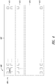
Figure 4 illustrates an embodiment of a memory array. -
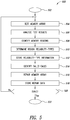
Figure 5 illustrates an embodiment of a method of generating a region reliability type memory map. -
Figure 6 illustrates an embodiment of a method of allocating memory in a memory array to a process based on region reliability type information. - In the following description, certain details are set forth in order to provide a thorough understanding of various embodiments of devices, systems, methods and articles. However, one of skill in the art will understand that other embodiments may be practiced without these details. In other instances, well-known structures and methods associated with, for example, circuits, such as transistors, multipliers, adders, dividers, comparators, transistors, integrated circuits, logic gates, finite state machines, memories, interfaces, bus systems, etc., have not been shown or described in detail in some figures to avoid unnecessarily obscuring descriptions of the embodiments.
- Unless the context requires otherwise, throughout the specification and claims which follow, the word "comprise" and variations thereof, such as "comprising," and "comprises," are to be construed in an open, inclusive sense, that is, as "including, but not limited to." Reference to "at least one of" shall be construed to mean either or both the disjunctive and the inclusive, unless the context indicates otherwise.
- Reference throughout this specification to "one embodiment," or "an embodiment" means that a particular feature, structure or characteristic described in connection with the embodiment is included in at least one embodiment. Thus, the appearances of the phrases "in one embodiment," or "in an embodiment" in various places throughout this specification are not necessarily referring to the same embodiment, or to all embodiments. Furthermore, the particular features, structures, or characteristics may be combined in any suitable manner in one or more embodiments to obtain further embodiments.
- The headings are provided for convenience only, and do not interpret the scope or meaning of this disclosure.
- The sizes and relative positions of elements in the drawings are not necessarily drawn to scale. For example, the shapes of various elements and angles are not drawn to scale, and some of these elements are enlarged and positioned to improve drawing legibility. Further, the particular shapes of the elements as drawn are not necessarily intended to convey any information regarding the actual shape of particular elements, and have been selected solely for ease of recognition in the drawings.
-
Figure 1 is a functional block diagram of an embodiment of an electronic device orsystem 100 of the type to which the embodiments which will be described may apply. Thesystem 100 comprises one or more processing cores orcircuits 102. Theprocessing cores 102 may comprise, for example, one or more processors, a state machine, a microprocessor, a programmable logic circuit, discrete circuitry, logic gates, registers, etc., and various combinations thereof. The processing cores may control overall operation of thesystem 100, execution of application programs by thesystem 100, etc. - The
system 100 includes one or more memories, such as one or more volatile and/or non-volatile memories which may store, for example, all or part of instructions and data related to control of thesystem 100, applications and operations performed by thesystem 100, etc. As illustrated, thesystem 100 includes one ormore cache memories 104, one or moreprimary memories 106, and one or moresecondary memories 108, each comprising memory management circuitry orMMUs 110. One or more of thememories memory array 302 ofFigure 3 ), which, in operation, may be shared by one or more processes executed by thesystem 100. Thememory management circuitry 110, in operation, employs one or more memory management routines to allocate regions (see, e.g.,regions 310 ofFigure 3 ,regions 410 ofFigure 4 ) of shared memory arrays (see, e.g.,memory array 302 ofFigure 3 ) to various processes executed by thesystem 100, for example as discussed in more detail with reference toFigures 2-6 . - The
system 100 may include one or more sensors 120 (e.g., accelerometers, pressure sensors, temperature sensors, etc), one or more interfaces 130 (e.g., wireless communication interfaces, wired communication interfaces, etc.), one ormore BIST circuits 140, andother circuits 150, which may include antennas, power supplies, etc., and amain bus system 160. Themain bus system 160 may include one or more data, address, power and/or control buses coupled to the various components of thesystem 100. Thesystem 100 also may include additional bus systems such asbus system 162, which communicatively couples thecache memory 104 and theprocessing core 102,bus system 164, which communicatively couples thecache memory 104 and theprimary memory 106,bus system 166, which communicatively couples theprimary memory 106 and theprocessing core 102, andbus system 168, which communicatively couples theprimary memory 106 and thesecondary memory 108. - The primary memory or
memories 106 are typically the working memory of the system 100 (e.g., the memory or memories upon which theprocessing cores 102 work), and may typically be a volatile memory (e.g., DRAM) of a limited size storing code and data related to processes executed by thesystem 100. For convenience, reference herein to data stored in a memory may also refer to code stored in a memory. Non-volatile memories, such as SRAM, ReRAM (e.g., PCM, MRAM), FRAM, etc., may be employed as or in the primary memory or memories in an embodiment. Thesecondary memory 108 may typically be a non-volatile memory, which stores instructions and data, which may be retrieved and stored in theprimary memory 106 when needed by thesystem 100. Thecache memory 104 may be a relatively fast memory compared to thesecondary memory 108 and typically has a limited size, which may be larger than a size of theprimary memory 106. - The
cache memory 104 temporarily stores code and data for later use by thesystem 100. Instead of retrieving needed code or data from thesecondary memory 108 for storage in theprimary memory 106, thesystem 100 may check thecache memory 104 first to see if the data or code is already stored in thecache memory 104. Acache memory 104 may significantly improve performance of a system, such as thesystem 100, by reducing the time and other resources needed to retrieve data and code for use by thesystem 100. When code and data are retrieved (e.g., from the secondary memory 108) for use by thesystem 100, or when data or code are written (e.g., to theprimary memory 106 or to the secondary memory 108), a copy of the data or code may be stored in thecache memory 104 for later use by thesystem 100. Various cache management routines may be employed to control the data stored in the cache memory ormemories 104. -
Figure 2 is a functional block diagram of another embodiment of an electronic device orsystem 200 of the type to which the embodiments which will be described may apply. Thesystem 200 may be used, for example, to implement an ANN to classify sensor data. It is noted that the embodiment ofFigure 1 may be employed to implement the embodiment ofFigure 2 , and may comprise a system on a chip. - The
system 200 comprises aglobal memory 202, which may serve for example as a primary memory (seeprimary memory 106 ofFigure 1 ), for bothANN 203 processes or clusters, and forhost system 204 processes or clusters. Theglobal memory 202 comprisesmemory management circuitry 206 and one or more sharedmemory arrays 208. Thememory management circuitry 206, in operation, employs one or more memory management routines to allocate regions of the sharedmemory arrays 208 to various processes executed by thesystem 200 based on request types and region reliability type information, for example as discussed in more detail with reference toFigures 3-6 . - As illustrated, the
ANN 203 comprises one ormore data movers 210, one ormore memory bridges 220, one ormore sensors 230 and corresponding sensor interfaces 232, one or moreconvolutional accelerator engines 240, and one or more fullyconnected engines 250, which may be implemented and operate in an otherwise conventional manner to produce aclassification output 260. - Efficient low power operation may be facilitated by using a hierarchical memory system and efficient reuse of local data. Accelerating CDNN convolutional layers may account for more than 90% of total operations. Efficient balancing of the computational and memory resources for both bandwidth and area may facilitate achieving better throughput without hitting associated ceilings. A design time configurable accelerator framework (CAF) (see
Figure 2 ) may be used based on unidirectional links transporting data streams via configurable data movers sources/sinks being I/O interfaces (e.g. cameras), memory hierarchies and various types of accelerators including the Convolution Accelerator (CA). - The
data movers 210, in operation, move data streams between IOs (e.g., sensor interfaces 232), memory hierarchies (e.g.,global memory 202, memory bridges 220),convolutional accelerators 240 and fullyconnected engines 250. In an embodiment, a full featured backpressure mechanism handles the data flow control and stream multicasting, facilitating the reuse of a data stream at multiple block instances. Linked lists may control the fully autonomous processing of entire convolution layers in ANN. Multiple accelerators may be grouped or chained to handle varying sizes for feature maps data and multiple kernels in parallel. - In an embodiment, the
convolutional accelerator engines 240 may comprise an array of clustered multiply-accumulate (MAC) units or circuits, which, in operation, implement the convolutional layer processing in ANN. The convolutional accelerator engines may include a line buffer to fetch multiple feature map data words in parallel with a single memory access. A register-based kernel buffer may be used which provides multiple read ports, while a plurality of multibit fixed point MAC units or circuits perform multiple MAC operations per clock cycle. An adder tree may be employed to sum the MAC results for each kernel column. An overlapping, column based calculation of the MAC operations facilitates an optimal reuse of the feature maps data for multiple MACs and reducing of the power dissipation associated with redundant memory accesses. - In some embodiments, the
system 100 or thesystem 200 may include more components than illustrated, may include fewer components than illustrated, may split illustrated components into separate components, may combine illustrated components, etc., and various combinations thereof. For example, thesecondary memory 108 ofFigure 1 may comprise an external memory coupled to thesystem 100 through an interface, in addition to or instead of an internal secondary memory. In some embodiments, theprimary memory 106 and thesecondary memory 108 may be combined into a single memory. In some embodiments, thecache memory 104 may be omitted. In another example, the one or moreprimary memories 106 may share common memory management circuitry, in addition to or instead ofseparate MMUs 110. - Conventionally, system memory hierarchies are tested to ensure reliable operation at certain minimum voltages based on statistical models and accumulated memory density. If the predicted error rate for a memory array of an integrated circuit chip exceeds a threshold error rate, the chip is discarded. The statistical error rates of memories tend to be higher when the memories are operated at lower minimum voltages.
- The inventors have realized that different processes or clusters sharing a memory array may tolerate different data error rates, and that this tolerance may be exploited to facilitate reducing overall system memory requirements, to increase chip yields, and to lower minimum operating voltages. For example, in an ANN system, a host process or cluster may, for practical purposes, need to employ memory having a lower error rate than needed by certain ANN processes or clusters. Thus, a higher overall error rate of a chip may be acceptable if the predicted failure rates for regions of the memory array are taken into consideration during allocation of memory of the memory array to different processes. A higher overall predicted failure rate facilitates reducing the number of rejected chips, lowering the amount of redundant memory employed, and operating chips using lower minimum operating voltages.
- In the context of embedded ANN systems, the bulk of the on-chip memory for the ANN system may be needed to store kernel data, intermediate partial sums, and feature data, which are relatively fault tolerant, while a smaller portion may be needed to store configuration/layer sequence data, which are less fault tolerant. Similarly, host system processes may be less fault tolerant. Thus, allocating memory, such as a shared memory, based on the type of memory request (e.g., the purpose for which the memory is being allocated) and the error or reliability characteristics of regions of the memory may facilitate significantly increasing the yield of the chip fabrication process. In addition, the amount of memory needed for redundancy may be reduced, because rows and columns which conventionally may have been designated as unusable and replaced by redundant memory may instead be designated for allocation to certain types of processes, reducing the need for redundant memory. Minimum operating voltages also may be reduced, facilitating reduced usage of power in, for example, mobile devices.
- An example structure of a
memory 300, which may, in operation, allocate memory regions based on allocation request types and information indicative of predicted or statistical data error rates of respective regions of memory arrays is shown inFigure 3 . Thememory 300 may be used, for example, to implement one or more of thecache memory 104, theprimary memory 106, and thesecondary memory 108 ofFigure 1 , theglobal memory 202 ofFigure 2 , etc. - The
memory 300 comprises one ormore memory arrays 302. As illustrated, thememory array 302 is organized into a plurality ofrows 304 andcolumns 306 ofmemory cells 308. Thememory array 302 also is organized into a plurality ofregions 310. Thememory array 302 may be organized intoregions 310 physically, logically, or various combinations thereof. Theregions 310 may be of a uniform size (e.g., of a uniform number ofrows 304 and columns 306), or of varying sizes. As illustrated, theregions 310 ofFigure 3 have a same number ofrows 304, but different numbers ofcolumns 306. Thememory array 302 also includes a plurality ofredundant columns 312, which may be used to replace failedcolumns 306 in thememory array 302. -
Figure 4 illustrates an embodiment of amemory array 402, which is similar to thememory array 302 ofFigure 3 . Theregions 410 ofFigure 4 have a same number ofcolumns 406 ofmemory cells 408, and different numbers ofrows 404. In an embodiment, eachregion 410 comprises a single row of thememory array 402. Thememory array 402 ofFigure 4 also has a plurality ofredundant rows 412, which may be used to replace failedrows 404 of thememory array 402. Thememory array 402 may be employed, for example, in the embodiment of thememory 300 ofFigure 3 , instead of or in addition to thememory array 302 ofFigure 3 . - Various types of memory may be employed as the
memory array 302 or thememory array 402. For example, dynamic random access memory (DRAM), static random access memory (SRAM), resistive random access memory (ReRAM) (e.g., phase-change memory (PCM), magnetic random access memory (MRAM), etc.), FRAM, etc., and various combinations thereof, may be employed. Multi-level memory cells (e.g., multilevel ReRAM cells) may be employed. - The
memory 300 ofFigure 3 also comprisesmemory management circuitry 320 including memorycontrol parameter storage 322. The memory control parameter storage includes one ormore memory cells 308, which as illustrated include a bank offuses 324. The memorycontrol parameter storage 322, in operation, stores memory control parameters associated withregions 310 of thememory array 302. Alternatively or additionally, a cut in thememory array 302 may be used to store memory control parameters or a separate memory may be employed. The memory control parameters may comprise tags, for example, associated with regions of the memory. - The stored memory control parameters include region reliability-type parameters, such as parameters indicative of types of processes to which a
region memory array respective regions 310 of thememory array 302, failure rates associated with operation at different voltage levels, failure rates associated with operation in different modes (e.g., multilevel mode or binary mode), etc. For example, predicted failure rates based on testing of the memory array may be employed to determine values of the region reliability-type parameters. The stored memory control parameters may include other parameters, such as indications of whether a region or a portion thereof is currently allocated to a particular process, or available for allocation, historical allocation information, etc. - The stored reliability-type parameters may be employed by the
memory management circuitry 320 to allocateavailable memory regions memory array memory region memory management circuitry 320 to be available for allocation to all processes and processors. Conversely, amemory region memory management circuitry 320 to be available for allocation only to certain processes or processors. For example, allocation of amemory region region 310 to less fault tolerant processes, such as ANN configuration/layer sequence data storage and host system processes, would be prevented. The reliability-type parameters may be stored as a memory map. - In some embodiments, the reliability-type parameter values may be binary values associated with a
region memory array - In some embodiments, the reliability-type parameters values may be values which indicate one of a plurality of reliability levels associated with a
region 310 of thememory 300. For example, a first value may indicate theregion 310 may be allocated to any process, a second value may indicate allocation of theregion 310 to host processes should be restricted, a third value may indicate allocation of theregion 310 to host processes and ANN configuration/layer sequence data storage should be restricted, and a fourth value may indicate allocation of theregion 310 to any process should be restricted. - In an embodiment, values of the region reliability type parameters may be stored in the bank of
fuses 324. Tables 1 and 2 below indicate example correspondences between fuse states and reliability-type values with respect to four regions of an example memory array. Typically, a memory array would have substantially more than four regions, for example, if each row of a memory array is considered a region.Table 1 Memory Region Associated With A Fuse Region of Memory Array Fuse state Reliability-type 1 (e.g., rows 0-4) Unblown Unrestricted 2 (e.g., rows 5-9) Blown Restricted 3 (e.g., rows 10-14) Blown Restricted 4 (e.g., rows 15-19) Unblown Unrestricted - In Table 1, each region of a memory array is associated with a fuse. As can be seen, allocation of regions 1 and 4 is unrestricted (e.g., regions 1 and 4 may be allocated in response to any allocation request type), while allocation of regions 2 and 3 is restricted (e.g., in response to ANN kernel data storage process requests). Conventionally, regions 2 and 3 or portions thereof (e.g., rows) may have instead been deemed unusable, and the chip rejected because the failure rate for the chip was too high. In some embodiments, allocation of regions of the memory array associated with unblown fuses may be restricted to process types needing low data error rates (e.g., host processes) and allocation of regions of the memory array associated with blown fuses may be restricted to process types which are more tolerant of data errors (e.g., ANN kernel data storage processes).
Table 2 Memory Region Associated With Two Fuses Region Fuse 1 Fuse 2 Reliability- Type 1 Unblown Unblown Level 0 Restriction (e.g., may be allocated to any process or request type) 2 Blown Unblown Level 1 Restriction (e.g., do not allocate to host processes or request types) 3 Blown Blown Level 2 Restriction (e.g., do not allocate to host processes or to ANN configuration/layer sequence data storage processes or request types) 4 Unblown Unblown Level 0 Restriction - In Table 2, each region of a memory array is associated with two fuses. As can be seen, regions 1 and 4 has a level 0 restriction, and may be allocated in response to any allocation request type. Region 2 has a level 1 restriction to prevent allocation in response to request types associated with host processes. Region 3 has a level 2 restriction to prevent allocation in response to request types associated with host processes or associated with ANN configuration/layer sequence data storage processes. In an embodiment, a state of fuse 1 as unblown and of fuse 2 as blown would not be employed. In some embodiments, allocation of regions of the memory array associated with certain fuse states may be restricted to request types associated with processes needing low data error rates (e.g., host processes) and allocation of regions of the memory array associated with other fuse states may be restricted to request types associated with processes which are more tolerant of data errors (e.g., ANN kernel data storage processes).
-
Figure 5 illustrates an embodiment of amethod 500 of generating region reliability-type and failure information associated with a memory array, for example, during an integrated circuit manufacturing process or a boot process of an integrated circuit. Themethod 500 ofFigure 5 will be described for convenience with reference toFigures 1-4 . - The
method 500 starts at 502. Themethod 500 may be started, for example, as part of test routine employed during a chip manufacturing process, as part of a chip boot process, etc. Themethod 500 proceeds from 502 to 504. - At 504, the
method 500 tests a memory array, such as thememory array 302 ofFigure 3 or thememory array 402 ofFigure 4 . This may be done, for example, using testing probes (not shown), BIST circuitry (seeBIST circuitry 140 ofFigure 1 ), testing routines, and various combinations thereof. Data patterns may be loaded into the memory array and read from the memory array to generate test results. The testing may include testing at various minimum operating voltage levels, in various operating modes (e.g., binary or multilevel mode, etc.). Themethod 500 proceeds from 504 to 506. - At 506, the
method 500 analyzes the results of the testing at 504. This may be done, for example, using BIST circuitry (seeBIST circuitry 140 ofFigure 1 ), statistical analysis of comparisons of the data read from the memory array to expected values, etc. For example, statistical failure rates of rows, columns or regions of the memory array may be determined based on statistical analysis of the results of the testing at 504. The method proceeds from 506 to 508. - At 508, the
method 500 identifies regions of the memory array. The regions may, for example, be default regions, e.g., every row may be identified as a separate region, every five rows may be identified as a separate region, every column may be identified as a separate region, etc. The regions may be identified based on the test results. For example, every ten rows in order with a threshold failure rate below a first threshold may be grouped together and identified as a region; every ten rows in order with a threshold failure rate above the first threshold and below a second threshold failure rate may grouped together and identified as a region; every row with a threshold failure rate above the second threshold may be identified a separate region; etc. Themethod 500 proceeds from 508 to 510. - At 510, the
method 500 determines region reliability-type information associated with the identified regions. For example, themethod 500 may classify each region in a binary manner as having an unrestricted reliability-type or a restricted reliability-type based on statistical failure rates associated with the regions. See, for example, the discussion of binary region reliability-type values with respect to Table 1, above. In another example, themethod 500 may classify each region to one of a plurality of reliability levels based on statistical failure rates associated with the respective regions, with respective regions in various operational modes, etc. See, for example, the discussion of region reliability levels with reference to Table 2, above. The statistical predicted failure rate of a region may be compared with one or more thresholds to determine the reliability-type of the region. The method proceeds from 510 to 512. - At 512, the
method 500 stores information indicate of the reliability-types of the regions. For example, memory control parameter values indicative of the reliability-type information associated with regions of the memory array may be stored in the memorycontrol parameter storage 322 ofmemory management circuitry 320 ofFigure 3 (e.g., stored in the bank offuses 324; stored as tags associated with regions of the memory array; etc.). The information indicative of the reliability-types of the regions may be stored as a memory map. The stored control parameter values may be used, for example, together with allocation request type information, to allocate regions of the memory to system processes, such ashost system 204 processes andANN 203 processes of thesystem 200 ofFigure 2 , etc. See, for example,Figure 6 and the description thereof. Themethod 500 proceeds from 512 to 514. - At 514, the
method 500 identifies failed cells in the memory array. In practice, this may be done, for example, by identifying failed rows (or columns) based on a comparison of statistical failure rates of the rows (columns) to a threshold failure rate. In comparison to conventional systems, the threshold failure rate may be higher (resulting in fewer failed rows) because a failure rate which conventionally would have resulted in the row being replaced with a redundant row, may instead be used to associate a reliability-type with the row. Themethod 500 proceeds from 514 to 516. - At 516, the
method 500 repairs the memory array using redundant memory. For example, a failedrow 404 ofmemory array 402 may be identified as unusable, andredundant row 412 identified as available for allocation to replace the failedrow 404. Themethod 500 proceeds from 516 to 518. - At 518, the
method 500 stores repair data associated with the memory array. For example, information identifying failed rows and redundant rows of thememory array 402 ofFigure 4 may be stored as a memory map, such as in the memorycontrol parameter storage 322 ofmemory management circuitry 320 ofFigure 3 . Themethod 500 proceeds from 518 to 520. - At 520, the
method 500 determines whether themethod 500 is finished or should continue. For example, when the memory array has been repaired at 516, themethod 500 may determine that themethod 500 is not finished in order to determine reliability information and failure information associated with redundant cells (e.g., redundant rows), used to replace failed cells in the memory array. When it is determined at 520 that themethod 500 is finished, themethod 500 proceeds from 520 to 522, whether themethod 500 may terminate, may perform other processes (such as error processing), etc. When it is not determined at 520 that themethod 500 is finished, themethod 500 proceeds to from 520 to 504. - Embodiments of methods of generating reliability-type information associated with a memory array may contain additional acts not shown in
Figure 5 , may not contain all of the acts shown inFigure 5 , may perform acts shown inFigure 5 in various orders, and may be modified in various respects. For example, themethod 500 may omitact 508 when default regions are employed; may combineacts acts acts -
Figure 6 illustrates an embodiment of amethod 600 of allocating memory of a shared memory to a process of a plurality of processes sharing the memory. Themethod 600 ofFigure 6 is described for convenience with reference toFigures 1-5 . To simplify the discussion, the embodiment ofFigure 6 is discussed with reference to a single memory array, such as thememory array 208 ofFigure 2 , thememory array 302 ofFigure 3 , thememory array 402 ofFigure 4 , etc. In some embodiments, themethod 600 may be employed to allocate memory in a plurality of memory arrays of a shared memory, in a plurality of shared memories, etc. - The
method 600 starts at 602. Themethod 600 may be started, for example, as part of memory management routine executing on a processing system, such as thesystem 100 ofFigure 1 , thesystem 200 ofFigure 2 , thehost system 204 ofFigure 2 , on memory management circuitry, such as thememory management circuitry 110 ofFigure 1 , 206 ofFigure 2 , 320 ofFigure 3 , etc. Themethod 600 may be employed to allocate memory for host processes, application processes, data buffers of host and application processes, etc., and may allocate memory when processes are initialized and dynamically during runtime. Themethod 600 proceeds from 602 to 604. - At 604, the
method 600 determines whether a request has been received to allocate memory of a shared memory array to a process. For example, a host system process or an application process, such as an ANN process, may request allocation of memory in a shared memory array. When it is not determined that a request has been received to allocate memory of a shared memory array, themethod 600 returns to 604 to wait for a request to allocate memory of the shared memory array. In response to receipt of a request to allocate memory of the shared memory array, themethod 600 proceeds from 604 to 606. - At 606, the
method 600 associates one or more request types with the received request to allocate memory. This may be done, for example, by parsing the received request to determine a request type, by determining an origin of the request, etc. For example, the request may include a process identifier, a process type, other information indicative of a request type to be associated with the received request, a request type field, etc. In another example, requests received from a first processor of a plurality of processors may be associated with a first request type, and requests received from another processor of the plurality of processor may be associated with a second request type. - In an embodiment, requests received from a host process may be associated with a first request type. Requests received from an ANN process may be associated with a second request type if the ANN process is a control ANN configuration/layer sequence data storage process, and associated with a third request type if the ANN process is requesting a buffer to store kernel data, intermediate partial sums, or feature data. Default memory allocation request types may be employed. The
method 600 proceeds from 606 to 608. - At 608, the
method 600 associates one or more region reliability-types with the received memory allocation request based on the determined request type associated with the received memory allocation request. For example, a memory allocation request associated with a first request type may be associated with a first region reliability-type and a memory allocation request associated with a second request type may be associated with a first and a second region reliability-type. Look-up tables may be employed to associate the received allocation request with one or more region reliability-types. Themethod 600 proceeds from 608 to 610. - At 610, the
method 600 allocates memory in a memory array in response to the memory allocation request based on the region reliability-types associated with the memory allocation request and stored information indicative of the region reliability-types of regions of the memory array. For example, themethod 600 may allocate all or part of one or more regions having a first region reliability-type in response to a memory request associated with the first region reliability type, and may allocate all or part of one or more regions having a first region reliability-type or a second region reliability-type in response to a memory request associated with the second region reliability-type. Stored information indicate of region reliability-types of regions of the memory array may be employed to select regions of the memory array to allocate in response to the memory allocation request. - For example, with reference to
Figures 2-4 and Table 1 (with the states of the fuses stored, for example, in the bank of fuses 324), a request from ahost system 204 may be associated at 606 with a request type indicating the allocation request is related to a process which is less tolerant of data errors. At 608, the request is associated with an unrestricted reliability type. At 610, based on the states of thefuses 324, themethod 600 may allocate all or part (e.g., with references toFigure 4 , one or more rows of a region 410) of region 1 and region 4 in response to the allocation request from thehost system 204; regions 2 and 3 would not be allocated in response to the request from the host system. A request received from anANN process 203 for a buffer to store kernel data, intermediate partial sums, or feature data may instead, at 606, be associated with a request type indicating the allocation request is related to a process which is more tolerant of data errors (e.g., a process less-sensitive to flipped bits). At 608, the request would be associated with a restricted reliability-type. At 610, based on the states of thefuses 324, themethod 600 may allocate all or part of one or more of region 1, region 2, region 3 and region 4 in response to the allocation request from the ANN process. - In another example, with reference to
Figures 2-4 and Table 2 (with the states of the fuses stored, for example, in the bank of fuses 324), a request from ahost system 204 may be associated at 606 with a request type indicating the allocation request is related to a process which is less tolerant of data errors. At 608, the request would be associated with reliability-type restriction level 0. At 610, based on the states of thefuses 324, themethod 600 may allocate rows of one or more of region 1 and region 4 in response to the allocation request from thehost system 204; rows from regions 2 and 3 would not be allocated in response to the request from the host system. A request received from anANN process 203 to store ANN configuration/layer sequence data may instead, at 606, be associated with a request type indicating the allocation request is related to a process which is moderately tolerant of data errors. At 608, the request is associated with reliability-type restriction level 1. At 610, based on the states of thefuses 324, themethod 600 may allocate rows of one or more of region 1, region 2 and region 4, but not region 3, in response to the allocation request from the ANN process to store ANN configuration/layer sequence data. A request received from anANN process 203 for a buffer to store kernel data, intermediate partial sums, or feature data may instead, at 606, be associated with a request type indicating the allocation request is related to a process which is more tolerant of data errors. At 608, the request is associated with reliability-type restriction level 2. At 610, based on the states of thefuses 324, themethod 600 may allocate all or part of one or more of region 1, region 2, region 3 and region 4 in response to the allocation request from the ANN process for a buffer to store kernel data, intermediate partial sums, or feature data. - Of course, the
method 600 may allocate regions of the memory array in response to an allocation request based on other factors in addition to the region reliability-type values associated with a memory allocation request, such as other memory control parameters, for example, stored in the memorycontrol parameter storage 322 ofFigure 3 , allocation selection routines designed to promote even wear of the memory, cache management control algorithms, limits on amounts of memory allocated to certain types of tasks, a total amount of unallocated memory available in the memory array, an operational mode of the memory region (e.g., multilevel, binary), etc., and various combinations thereof. Other memory management routines may be employed (e.g., error processing routines, routines to release allocated memory when no longer needed by a process, etc.) - The
method 600 proceeds from 610 to 612, where themethod 600 determines whether allocation of memory in the memory array is finished or should continue. When it is determined at 612 that themethod 600 is finished, themethod 600 proceeds from 612 to 614, whether themethod 600 may terminate, may perform other processes (such as error processing), etc. When it is not determined at 612 that themethod 600 is finished, themethod 600 proceeds to from 612 to 604. - Embodiments of methods of allocating memory of a shared memory may contain additional acts not shown in
Figure 6 , may not contain all of the acts shown inFigure 6 , may perform acts shown inFigure 6 in various orders, and may be modified in various respects. For example, themethod 600 may combineacts - Some embodiments may take the form of or comprise computer program products. For example, according to one embodiment there is provided a computer readable medium comprising a computer program adapted to perform one or more of the methods or functions described above. The medium may be a physical storage medium, such as for example a Read Only Memory (ROM) chip, or a disk such as a Digital Versatile Disk (DVD-ROM), Compact Disk (CD-ROM), a hard disk, a memory, a network, or a portable media article to be read by an appropriate drive or via an appropriate connection, including as encoded in one or more barcodes or other related codes stored on one or more such computer-readable mediums and being readable by an appropriate reader device.
- Furthermore, in some embodiments, some or all of the methods and/or functionality may be implemented or provided in other manners, such as at least partially in firmware and/or hardware, including, but not limited to, one or more application-specific integrated circuits (ASICs), digital signal processors, discrete circuitry, logic gates, standard integrated circuits, controllers (e.g., by executing appropriate instructions, and including microcontrollers and/or embedded controllers), field-programmable gate arrays (FPGAs), complex programmable logic devices (CPLDs), etc., as well as devices that employ RFID technology, and various combinations thereof.
- The various embodiments described above can be combined to provide further embodiments. Aspects of the embodiments can be modified, if necessary to employ concepts of the various embodiments and publications to provide yet further embodiments.
- These and other changes can be made to the embodiments in light of the above-detailed description. In general, in the following claims, the terms used should not be construed to limit the claims to the specific embodiments disclosed in the specification and the claims, but should be construed to include all possible embodiments along with the full scope of equivalents to which such claims are entitled. Accordingly, the claims are not limited by the disclosure.
Claims (34)
- A device, comprising:one or more memory cells, which, in operation, store information indicative of reliability-types of regions of a memory array; andmemory management circuitry coupled to the one or more memory cells, wherein the memory management circuitry, in operation, responds to a request to allocate memory in the memory array to a process by:determining a request type associated with the request to allocate memory; andallocating memory in the memory array to the process based on the request type associated with the request to allocate memory and the stored information indicative of reliability-types of regions of the memory array.
- The device of claim 1 wherein the one or more memory cells comprise a bank of fuses.
- The device of claim 2 wherein each fuse is associated with a respective region of the memory array.
- The device of claim 1 wherein the one or more cells, in operation, store the information indicative of reliability-types of regions of the memory array as a memory map.
- The device of claim 1 wherein the determining a request type comprises determining a type of process associated with the request.
- The device of claim 5 wherein the memory array is a shared memory array and the memory management circuitry, in operation:
responds to a request received from a host system process by allocating from one or more regions of the memory array which the stored reliability information indicates has a first reliability-type. - The device of claim 6 wherein the memory management circuitry, in operation:
responds to a request received from an application process by allocating from one or more regions of the memory array which the stored reliability information indicates has the first reliability-type or a second reliability type, the second reliability type indicating the region is less-reliable than a region having the first reliability-type. - The device of claim 6 wherein the memory management circuitry, in operation:responds to a request received from an artificial neural network (ANN) control process by allocating from one or more regions of the memory array which the stored reliability information indicates has the first reliability-type; andresponds to a request from an ANN process to allocate memory to a memory buffer to store kernel data, intermediate partial sums, or feature data by allocating from one or more regions of the memory array which the stored reliability information indicates has the first reliability-type or a second reliability type, the second reliability type indicating the region is less-reliable than a region having the first reliability-type.
- The device of claim 1 wherein the stored information indicative of reliability-types of regions of the memory array indicates one of a plurality of reliability levels associated with regions of the memory array.
- The device of claim 1 wherein the memory array is organized into rows and columns of memory cells, and a region is a row of the memory array.
- The device of claim 1, comprising built-in-self-test circuitry, which, in operation, periodically:tests the memory array; andupdates the stored information indicative of the reliability of regions of the memory array based on results of the testing.
- The device of claim 1 wherein the one or more memory cells comprise a cut in the shared memory array.
- The device of claim 1 wherein the one or more memory cells comprise cells of a non-volatile memory.
- The device of claim 1 wherein the memory array comprises an array of non-volatile memory cells.
- The device of claim 14 wherein the array of non-volatile memory cells comprise one or more of:SRAM memory cells;ReRAM memory cells; andFRAM memory cells.
- The device of claim 14 wherein the array of non-volatile memory cells comprises one or more multilevel ReRAM memory cells.
- A system, comprising:a memory array; andmemory management circuitry coupled to the memory array, wherein the memory management circuitry, in operation, responds to a request to allocate memory in the memory array to a process of a plurality of processes by:determining a request type associated with the request to allocate memory; andallocating memory in the memory array to the process based on the request type associated with the request to allocate memory and stored information indicative of reliability-types of regions of the memory array.
- The system of claim 17 wherein the memory management circuitry comprises a bank of fuses, which, in operation, store the information indicative of reliability-types of regions of the memory array.
- The system of claim 18 wherein each fuse is associated with a respective region of the memory array.
- The system of claim 17 wherein the determining a request type comprises determining a type of process associated with the request.
- The system of claim 20, comprising one or more processing cores executing the plurality of processes, wherein the memory management circuitry, in operation:
responds to a request received from a host system process of the plurality of processes by allocating from one or more regions of the memory array which the stored reliability information indicates has a first reliability-type. - The system of claim 21 wherein the memory management circuitry, in operation:responds to a request received from an artificial neural network (ANN) control process by allocating from one or more regions of the memory array which the stored reliability information indicates has the first reliability-type; andresponds to a request from an ANN process to allocate memory to a memory buffer to store kernel data, intermediate partial sums, or feature data by allocating from one or more regions of the memory array which the stored reliability information indicates has the first reliability-type or a second reliability type, the second reliability type indicating the region is less-reliable than a region having the first reliability-type.
- The system of claim 17 wherein the stored information indicative of reliability-types of regions of the memory array indicates one of a plurality of reliability levels associated with regions of the memory array.
- A method, comprising:storing information indicative of reliability-types of regions of a memory array; andresponding to a request to allocate memory in the memory array to a process of a plurality of processes by:determining a request type associated with the request to allocate memory in the memory array; andallocating memory in the memory array to the process based on the request type associated with the request to allocate memory in the memory array and the stored information indicative of reliability-types of regions of the memory array.
- The method of claim 24 wherein the storing information indicative of reliability types of regions of the shared memory array comprises blowing fuses in a bank of fuses associated with the memory array.
- The method of claim 24 wherein the determining a request type comprises determining a type of process associated with the request.
- The method of claim 26, comprising:
responding to a request received from a host system process of the plurality of processes by allocating from one or more regions of the memory array which the stored reliability information indicates has a first reliability-type. - The method of claim 27, comprising:responding to a request received from an artificial neural network (ANN) control process by allocating from one or more regions of the memory array which the stored reliability information indicates has the first reliability-type; andresponding to a request from an ANN process to allocate memory to a memory buffer to store kernel data, intermediate partial sums, or feature data by allocating from one or more regions of the memory array which the stored reliability information indicates has the first reliability-type or a second reliability type, the second reliability type indicating the region is less-reliable than a region having the first reliability-type.
- The method of claim 24, comprising:testing the memory array; andgenerating the stored information indicative of reliability-types of regions of the memory array based on results of the testing.
- The method of claim 29 wherein the testing is performed at a wafer level.
- The method of claim 29, comprising:retesting the memory array; andupdating the stored information indicative of reliability-types of regions of the memory array based on results of the retesting.
- A non-transitory computer-readable medium having contents which cause memory management circuitry to respond to a request to allocate memory in a memory array to a process of a plurality of processes by:determining a request type associated with the request to allocate memory in the memory array; andallocating memory in the memory array to the process based on the request type associated with the request to allocate memory in the memory array and stored information indicative of reliability-types of regions of the memory array.
- The non-transitory computer-readable medium of claim 32 wherein the contents comprising instructions executed by the memory management circuitry.
- The non-transitory computer-readable medium of claim 32 wherein the plurality of processes include host system processes and artificial neural network processes.
Applications Claiming Priority (2)
| Application Number | Priority Date | Filing Date | Title |
|---|---|---|---|
| US201962866429P | 2019-06-25 | 2019-06-25 | |
| US16/894,527 US11257543B2 (en) | 2019-06-25 | 2020-06-05 | Memory management device, system and method |
Publications (1)
| Publication Number | Publication Date |
|---|---|
| EP3757797A1 true EP3757797A1 (en) | 2020-12-30 |
Family
ID=71096602
Family Applications (1)
| Application Number | Title | Priority Date | Filing Date |
|---|---|---|---|
| EP20180031.5A Pending EP3757797A1 (en) | 2019-06-25 | 2020-06-15 | Memory management device, system and method |
Country Status (3)
| Country | Link |
|---|---|
| US (2) | US11257543B2 (en) |
| EP (1) | EP3757797A1 (en) |
| CN (1) | CN112133360B (en) |
Families Citing this family (2)
| Publication number | Priority date | Publication date | Assignee | Title |
|---|---|---|---|---|
| CN112837736A (en) * | 2021-03-16 | 2021-05-25 | 江苏时代全芯存储科技股份有限公司 | Memory device and repairing method thereof |
| US12147320B2 (en) * | 2022-09-30 | 2024-11-19 | Micron Technology, Inc. | Systems and methods of tiered data storage and processing and decision making |
Citations (7)
| Publication number | Priority date | Publication date | Assignee | Title |
|---|---|---|---|---|
| US6205063B1 (en) * | 1998-08-26 | 2001-03-20 | International Business Machines Corporation | Apparatus and method for efficiently correcting defects in memory circuits |
| US9558107B2 (en) * | 2013-12-24 | 2017-01-31 | International Business Machines Corporation | Extending useful life of a non-volatile memory by health grading |
| US20170185478A1 (en) * | 2014-07-29 | 2017-06-29 | Sony Corporation | Memory controller, storage apparatus, information processing system, and memory controller control method |
| US20190042966A1 (en) * | 2018-05-05 | 2019-02-07 | Justin Hogaboam | Apparatus and method including a thermal noise adaptive scheduler for controlling a quantum computer |
| US20190056987A1 (en) * | 2017-08-17 | 2019-02-21 | Syntiant | Digital backed flash refresh |
| US20190068220A1 (en) * | 2017-08-29 | 2019-02-28 | Sk Hynix Memory Solutions Inc. | Memory system with ldpc decoder and method of operating such memory system and ldpc decoder |
| US20190073259A1 (en) * | 2017-09-06 | 2019-03-07 | Western Digital Technologies, Inc. | Storage of neural networks |
Family Cites Families (25)
| Publication number | Priority date | Publication date | Assignee | Title |
|---|---|---|---|---|
| US8027194B2 (en) * | 1988-06-13 | 2011-09-27 | Samsung Electronics Co., Ltd. | Memory system and method of accessing a semiconductor memory device |
| JP3178909B2 (en) * | 1992-01-10 | 2001-06-25 | 株式会社東芝 | Semiconductor memory device |
| JP3313576B2 (en) * | 1996-04-25 | 2002-08-12 | エヌイーシービューテクノロジー株式会社 | Memory access control method and device |
| KR100712596B1 (en) * | 2005-07-25 | 2007-04-30 | 삼성전자주식회사 | Method and device for repairing and trimming flash memory devices |
| US7647536B2 (en) | 2005-12-30 | 2010-01-12 | Intel Corporation | Repair bits for a low voltage cache |
| US7864587B2 (en) * | 2008-09-22 | 2011-01-04 | Micron Technology, Inc. | Programming a memory device to increase data reliability |
| US8386723B2 (en) * | 2009-02-11 | 2013-02-26 | Sandisk Il Ltd. | System and method of host request mapping |
| US9324433B2 (en) | 2011-04-25 | 2016-04-26 | Microsoft Technology Licensing, Llc | Intelligent flash reprogramming |
| US8605527B2 (en) | 2011-07-20 | 2013-12-10 | Taiwan Semiconductor Manufacturing Company, Ltd. | Mechanisms for built-in self test and repair for memory devices |
| US9953725B2 (en) * | 2012-02-29 | 2018-04-24 | Samsung Electronics Co., Ltd. | Semiconductor memory devices and methods of operating the same |
| US9047171B2 (en) | 2012-09-29 | 2015-06-02 | Intel Corporation | Differentiating cache reliability to reduce minimum on-die voltage |
| CN104346234B (en) * | 2013-08-09 | 2017-09-26 | 华为技术有限公司 | A kind of method of internal storage access, equipment and system |
| US9323614B2 (en) | 2013-11-06 | 2016-04-26 | Wisconsin Alumni Research Foundation | Dynamic error handling for on-chip memory structures |
| US9786356B2 (en) | 2015-01-30 | 2017-10-10 | Qualcomm Incorporated | Memory device with adaptive voltage scaling based on error information |
| US20170110194A1 (en) | 2015-10-19 | 2017-04-20 | Silicon Storage Technology, Inc. | Power Driven Optimization For Flash Memory |
| CN108268941B (en) * | 2017-01-04 | 2022-05-31 | 意法半导体股份有限公司 | Deep Convolutional Network Heterogeneous Architecture |
| US9747158B1 (en) * | 2017-01-13 | 2017-08-29 | Pure Storage, Inc. | Intelligent refresh of 3D NAND |
| US20180285732A1 (en) | 2017-03-30 | 2018-10-04 | Intel Corporation | Selective noise tolerance modes of operation in a memory |
| US10347357B2 (en) | 2017-04-24 | 2019-07-09 | Intel Corporation | Post-packaging environment recovery of graphics on-die memory |
| US9912352B1 (en) | 2017-06-06 | 2018-03-06 | Western Digital Technologies, Inc. | Hamming distance based binary representations of numbers |
| US10607715B2 (en) | 2017-06-13 | 2020-03-31 | International Business Machines Corporation | Self-evaluating array of memory |
| US10877827B2 (en) | 2017-09-15 | 2020-12-29 | Pure Storage, Inc. | Read voltage optimization |
| JP6991084B2 (en) * | 2018-03-22 | 2022-01-12 | キオクシア株式会社 | Non-volatile memory device and control method |
| KR102587648B1 (en) * | 2018-07-23 | 2023-10-11 | 삼성전자주식회사 | Stacked memory devices, memory systems including the same and methods of testing the stacked memory devices |
| US11360667B2 (en) | 2019-09-09 | 2022-06-14 | Stmicroelectronics S.R.L. | Tagged memory operated at lower vmin in error tolerant system |
-
2020
- 2020-06-05 US US16/894,527 patent/US11257543B2/en active Active
- 2020-06-15 EP EP20180031.5A patent/EP3757797A1/en active Pending
- 2020-06-24 CN CN202010591159.0A patent/CN112133360B/en active Active
-
2022
- 2022-01-18 US US17/578,086 patent/US11749343B2/en active Active
Patent Citations (7)
| Publication number | Priority date | Publication date | Assignee | Title |
|---|---|---|---|---|
| US6205063B1 (en) * | 1998-08-26 | 2001-03-20 | International Business Machines Corporation | Apparatus and method for efficiently correcting defects in memory circuits |
| US9558107B2 (en) * | 2013-12-24 | 2017-01-31 | International Business Machines Corporation | Extending useful life of a non-volatile memory by health grading |
| US20170185478A1 (en) * | 2014-07-29 | 2017-06-29 | Sony Corporation | Memory controller, storage apparatus, information processing system, and memory controller control method |
| US20190056987A1 (en) * | 2017-08-17 | 2019-02-21 | Syntiant | Digital backed flash refresh |
| US20190068220A1 (en) * | 2017-08-29 | 2019-02-28 | Sk Hynix Memory Solutions Inc. | Memory system with ldpc decoder and method of operating such memory system and ldpc decoder |
| US20190073259A1 (en) * | 2017-09-06 | 2019-03-07 | Western Digital Technologies, Inc. | Storage of neural networks |
| US20190042966A1 (en) * | 2018-05-05 | 2019-02-07 | Justin Hogaboam | Apparatus and method including a thermal noise adaptive scheduler for controlling a quantum computer |
Also Published As
| Publication number | Publication date |
|---|---|
| US11749343B2 (en) | 2023-09-05 |
| US20200411089A1 (en) | 2020-12-31 |
| US20220139453A1 (en) | 2022-05-05 |
| US11257543B2 (en) | 2022-02-22 |
| CN112133360B (en) | 2024-09-13 |
| CN112133360A (en) | 2020-12-25 |
Similar Documents
| Publication | Publication Date | Title |
|---|---|---|
| US10446253B2 (en) | Semiconductor memory device and repair method thereof | |
| US10936391B2 (en) | Memory management method and storage controller | |
| KR20110001883A (en) | Bit error threshold and content addressable memory to address the remapped memory device | |
| US20210072894A1 (en) | Tagged memory operated at lower vmin in error tolerant system | |
| US9007856B2 (en) | Repair control circuit and semiconductor memory device including the same | |
| US9396817B2 (en) | Self-repairing memory and method of use | |
| US11749343B2 (en) | Memory management device, system and method | |
| CN104699577A (en) | Counter to locate faulty die in a distributed codeword storage system | |
| US8689081B2 (en) | Techniques for embedded memory self repair | |
| US20080049522A1 (en) | Content addressable memory entry coding for error detection and correction | |
| JP2000311497A (en) | Semiconductor storage device | |
| US10916325B2 (en) | Memory chip and test system including the same | |
| US11537464B2 (en) | Host-based error correction | |
| US20140369143A1 (en) | Apparatuses and methods for mapping memory addresses to redundant memory | |
| CN107068195A (en) | Three-dimensional chip and fault restoration and method for reading data with fault restoration device | |
| US11899971B2 (en) | Method for reading and writing and memory device | |
| US20190081640A1 (en) | Faulty word line and faulty bit line information in error correcting coding | |
| Lu et al. | Synergistic reliability and yield enhancement techniques for embedded SRAMs | |
| Oh et al. | BIRA with optimal repair rate using fault-free memory region for area reduction | |
| US8819391B1 (en) | Memory controller with enhanced block management techniques | |
| KR102900763B1 (en) | Repair circuit and memory device including the same | |
| Jang et al. | Adaptive weight-bit inversion for state error reduction for robust and efficient deep neural network inference using MLC NAND Flash | |
| CN103514961B (en) | Selfreparing memorizer, the calculating device comprising this memorizer and the method for operation memorizer | |
| US12237033B2 (en) | Component overprovisioning in layered devices | |
| US12625764B2 (en) | Memory device bad column identification and compensation |
Legal Events
| Date | Code | Title | Description |
|---|---|---|---|
| PUAI | Public reference made under article 153(3) epc to a published international application that has entered the european phase |
Free format text: ORIGINAL CODE: 0009012 |
|
| STAA | Information on the status of an ep patent application or granted ep patent |
Free format text: STATUS: REQUEST FOR EXAMINATION WAS MADE |
|
| 17P | Request for examination filed |
Effective date: 20200615 |
|
| AK | Designated contracting states |
Kind code of ref document: A1 Designated state(s): AL AT BE BG CH CY CZ DE DK EE ES FI FR GB GR HR HU IE IS IT LI LT LU LV MC MK MT NL NO PL PT RO RS SE SI SK SM TR |
|
| AX | Request for extension of the european patent |
Extension state: BA ME |
|
| STAA | Information on the status of an ep patent application or granted ep patent |
Free format text: STATUS: EXAMINATION IS IN PROGRESS |
|
| 17Q | First examination report despatched |
Effective date: 20220623 |
|
| GRAJ | Information related to disapproval of communication of intention to grant by the applicant or resumption of examination proceedings by the epo deleted |
Free format text: ORIGINAL CODE: EPIDOSDIGR1 |
|
| STAA | Information on the status of an ep patent application or granted ep patent |
Free format text: STATUS: GRANT OF PATENT IS INTENDED |
|
| GRAP | Despatch of communication of intention to grant a patent |
Free format text: ORIGINAL CODE: EPIDOSNIGR1 |
|
| GRAJ | Information related to disapproval of communication of intention to grant by the applicant or resumption of examination proceedings by the epo deleted |
Free format text: ORIGINAL CODE: EPIDOSDIGR1 |
|
| GRAP | Despatch of communication of intention to grant a patent |
Free format text: ORIGINAL CODE: EPIDOSNIGR1 |
|
| INTG | Intention to grant announced |
Effective date: 20260122 |
|
| INTG | Intention to grant announced |
Effective date: 20260209 |
|
| GRAS | Grant fee paid |
Free format text: ORIGINAL CODE: EPIDOSNIGR3 |
|
| GRAA | (expected) grant |
Free format text: ORIGINAL CODE: 0009210 |
|
| STAA | Information on the status of an ep patent application or granted ep patent |
Free format text: STATUS: THE PATENT HAS BEEN GRANTED |