EP3756066B1 - Electronic stylus with retention mechanism that charges battery from computing device - Google Patents
Electronic stylus with retention mechanism that charges battery from computing device Download PDFInfo
- Publication number
- EP3756066B1 EP3756066B1 EP19744932.5A EP19744932A EP3756066B1 EP 3756066 B1 EP3756066 B1 EP 3756066B1 EP 19744932 A EP19744932 A EP 19744932A EP 3756066 B1 EP3756066 B1 EP 3756066B1
- Authority
- EP
- European Patent Office
- Prior art keywords
- computing device
- retention mechanism
- electronic stylus
- spring
- electrically conductive
- Prior art date
- Legal status (The legal status is an assumption and is not a legal conclusion. Google has not performed a legal analysis and makes no representation as to the accuracy of the status listed.)
- Active
Links
Images


Classifications
-
- G—PHYSICS
- G06—COMPUTING OR CALCULATING; COUNTING
- G06F—ELECTRIC DIGITAL DATA PROCESSING
- G06F3/00—Input arrangements for transferring data to be processed into a form capable of being handled by the computer; Output arrangements for transferring data from processing unit to output unit, e.g. interface arrangements
- G06F3/01—Input arrangements or combined input and output arrangements for interaction between user and computer
- G06F3/03—Arrangements for converting the position or the displacement of a member into a coded form
- G06F3/033—Pointing devices displaced or positioned by the user, e.g. mice, trackballs, pens or joysticks; Accessories therefor
- G06F3/0354—Pointing devices displaced or positioned by the user, e.g. mice, trackballs, pens or joysticks; Accessories therefor with detection of two-dimensional [2D] relative movements between the device, or an operating part thereof, and a plane or surface, e.g. 2D mice, trackballs, pens or pucks
- G06F3/03545—Pens or stylus
-
- G—PHYSICS
- G06—COMPUTING OR CALCULATING; COUNTING
- G06F—ELECTRIC DIGITAL DATA PROCESSING
- G06F1/00—Details not covered by groups G06F3/00 - G06F13/00 and G06F21/00
- G06F1/26—Power supply means, e.g. regulation thereof
- G06F1/266—Arrangements to supply power to external peripherals either directly from the computer or under computer control, e.g. supply of power through the communication port, computer controlled power-strips
-
- G—PHYSICS
- G06—COMPUTING OR CALCULATING; COUNTING
- G06F—ELECTRIC DIGITAL DATA PROCESSING
- G06F3/00—Input arrangements for transferring data to be processed into a form capable of being handled by the computer; Output arrangements for transferring data from processing unit to output unit, e.g. interface arrangements
- G06F3/01—Input arrangements or combined input and output arrangements for interaction between user and computer
- G06F3/03—Arrangements for converting the position or the displacement of a member into a coded form
- G06F3/033—Pointing devices displaced or positioned by the user, e.g. mice, trackballs, pens or joysticks; Accessories therefor
- G06F3/038—Control and interface arrangements therefor, e.g. drivers or device-embedded control circuitry
-
- G—PHYSICS
- G06—COMPUTING OR CALCULATING; COUNTING
- G06F—ELECTRIC DIGITAL DATA PROCESSING
- G06F3/00—Input arrangements for transferring data to be processed into a form capable of being handled by the computer; Output arrangements for transferring data from processing unit to output unit, e.g. interface arrangements
- G06F3/01—Input arrangements or combined input and output arrangements for interaction between user and computer
- G06F3/03—Arrangements for converting the position or the displacement of a member into a coded form
- G06F3/041—Digitisers, e.g. for touch screens or touch pads, characterised by the transducing means
-
- H—ELECTRICITY
- H02—GENERATION; CONVERSION OR DISTRIBUTION OF ELECTRIC POWER
- H02J—ELECTRIC POWER NETWORKS; CIRCUIT ARRANGEMENTS OR SYSTEMS FOR SUPPLYING OR DISTRIBUTING ELECTRIC POWER; SYSTEMS FOR STORING ELECTRIC ENERGY
- H02J7/00—Circuit arrangements for charging or discharging batteries or for supplying loads from batteries
- H02J7/70—Circuit arrangements for charging or discharging batteries or for supplying loads from batteries characterised by the mechanical construction
- H02J7/751—Circuit arrangements for charging or discharging batteries or for supplying loads from batteries characterised by the mechanical construction concerning the insertion or the connection of the batteries
-
- G—PHYSICS
- G06—COMPUTING OR CALCULATING; COUNTING
- G06F—ELECTRIC DIGITAL DATA PROCESSING
- G06F2200/00—Indexing scheme relating to G06F1/04 - G06F1/32
- G06F2200/16—Indexing scheme relating to G06F1/16 - G06F1/18
- G06F2200/163—Indexing scheme relating to constructional details of the computer
- G06F2200/1632—Pen holder integrated in the computer
Definitions
- This description relates to electronic styluses.
- Electronic styluses as for example disclosed in US 2018/188834 A1 or US 2014/078116 A1 can be used to provide input to computing devices, enabling a user to provide input to the computing device as if drawing on a piece of paper.
- Active styluses which transmit signals indicating a location of the stylus, can include electronic components that make the stylus too thick to store inside the computing device.
- the invention provides an electronic stylus according to claim 1.
- the invention provides a method according to claim 9.
- the invention provides a computing device according to claim 11.
- a system is provided according to claim 14.
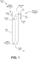
- FIG. 1 is a diagram of an electronic stylus according to an example embodiment.
- the electronic stylus 100 has an elongated body 102, being longer in a first direction from a writing end portion 104 to a back end portion 106 than in a second direction perpendicular to the first direction.
- the back end portion 106 can be opposite from the writing end portion.
- a diameter of the writing end portion 104 can narrow as a distance of the writing end portion 104 from the back end portion increases.
- the writing end portion 104 can be conical or rounded.
- a user can place the stylus 100 near or on a display of a computing device (shown in subsequent figures) to provide input to the computing device, treating the stylus 100 like a pen to write on the display.
- the stylus 110 can include a location transmitter 110, proximal to the writing end portion 104 and/or closer to the writing end portion 104 than to the back end portion 106.
- the location transmitter 110 can indicate to the computing device the location of the stylus 100, and the computing device can respond, such as by a drawing program adding lines or other graphical output to portions of the display proximal to the stylus 100.
- the stylus 100 includes a rechargeable battery 108.
- the rechargeable battery 108 can provide power to the location transmitter 110.
- the rechargeable battery 108 can recharge by receiving current and/or electricity from the computing device.
- the stylus 100 includes a retention mechanism 113.
- the retention mechanism 113 can be disposed closer to the back end portion 106 of the stylus 100 than to the writing end portion 104 of the stylus 100.
- the retention mechanism 113 can include a first arm portion 114 and a second arm portion 116.
- the first arm portion 114 can extend away from the elongated body 102.
- the second arm portion 116 can extend from the first arm portion 114 in a direction that is parallel to the direction that the elongated body 102 extends, such as from the back end portion 106 to the writing end portion 104.
- first arm portion 114 and the second arm portion 116 can be connected to form an L-shaped retention mechanism.
- the arms 114, 116 can be connected to form a right angle at a point where the two arms 114, 116 are connected to each other and/or are integrally formed.
- the retention mechanism 113 is not L-shaped, but can be other shapes due to the lengths of the arm portions 114, 116.
- the retention mechanism 113 includes an electrically conductive contact 112.
- the electrically conductive contact 112 can electrically couple the battery 108 to a power source in the computing device, enabling the battery 108 to receive power from the computing device.
- the electrically conductive contact 112 can extend into and/or through the first and second arm portions 114, 116. In a biased state, the electrically conductive contact 112 can extend beyond the second arm portion 116. The extension of the electrically conductive contact 112 beyond the second arm portion 116 can secure the stylus 100 to the computing device, as shown and described with respect to FIGs. 3 and 6B .
- the stylus 100 also includes a release mechanism 117.
- the release mechanism 117 can release the stylus 100 from the computing device.
- the release mechanism 117 causes the electrically conductive contact 112 to retract within and/or into the retention mechanism 113 so that the stylus 100 is no longer secured to the computing device.
- the release mechanism 117 can, for example, cause the electrically conductive contact 112 to retract into and/or within the second arm portion 116 of the retention mechanism 113.
- the release mechanism 117 can include a button 118.
- the button 118 can cause the electrically conductive contact 112 to retract into and/or within the retention mechanism 113 and/or second arm portion 116 in response to pressure applied to the button 118.
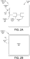
- FIG. 2A is a cutout view of a computing device 200 according to an example embodiment.
- the computing device 200 can interact with the stylus 100 by receiving input from the stylus 100, such as indications of locations of the stylus 100 near and/or on a display 222 (shown in FIG. 2B ) of the computing device, by securing the stylus 100 to the computing device 200, and/or by recharging the stylus 100.
- the computing device 200 includes a processor 212.
- the processor 212 can execute instructions such as instructions stored in memory.
- the memory may be included in the processor, or in a separate device included in the computing device 200.
- the computing device 200 includes a power source 210.
- the power source 210 can provide power to components of the computing device 200 such as the processor 212 and/or the display 222.
- the power source 210 can also provide power to the battery 108 and/or recharge the battery 108.
- the computing device 200 includes a charging pad 208.
- the charging pad 208 is coupled to the power source 210.
- the charging pad 208 contacts the electrically conductive contact 112 of the stylus 100 when the stylus 100 is secured to the computing device 200.
- the charging pad 208 can conduct electricity from the power source 210 to the battery 108 via the electrically conductive contact 112 when the stylus 100 is secured to the computing device 200, recharging the battery 108.
- the computing device 200 includes a chassis 202.
- the chassis 202 encloses, surrounds and/or supports components and/or devices of the computing device 200, such as the processor 212 and power source 210.
- the chassis 202 defines an aperture 204.
- the aperture 204 can receive the retention mechanism 113, which can include the arm portions 114, 116, when the stylus 100 is secured to the computing device 200.
- the computing device 200 includes a cover 206.
- the cover 206 can fit inside and/or fill the aperture 204.
- the cover 206 is spring-loaded, and biased, to rest in the aperture 204. In the biased position, the cover 206 can be flush with an outer portion of the chassis 202, creating a smooth appearance from outside the computing device 200.
- the cover 206 is be adjacent to the charging pad 208.
- the retention mechanism 113 which can include the arm portions 114, 116, can press the cover 206 into an interior portion of the computing device 200.
- the retention mechanism 113 can occupy some of the space previously occupied by the cover 206.
- the electrically conductive contact 112 can engage and/or contact the charging pad 208, electrically coupling the electrically conductive contact 112 to the charging pad 208 and enabling current to flow from the power source 210 to the battery 108.
- FIG. 2B is a top view of the computing device 200 according to an example embodiment.
- the computing device 200 can include a display 222.
- the display 222 can be surrounded and/or supported by a border 220.
- the border 220 can be surrounded and/or supported by the chassis 202.
- the display 222 can present graphical output.
- the display 222 can also receive input, such as touch input and/or input from the stylus 100.
- the display 222 can, for example, receive signals from the location transmitter 110 indicating a location of the stylus 100 and/or location transmitter 110 with respect to the display 222.
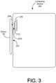
- FIG. 3 is a diagram showing the stylus 100 secured in the computing device 200 according to an example embodiment.
- the retention mechanism 113 of the stylus 100 has entered the computing device 200 through the aperture 204.
- a portion of the retention mechanism 113, such as the second arm portion 116, is in contact with the cover 206 and pressed the cover 206 into the computing device 200.
- the electrically conductive contact 112 is in contact with the conductive pad 208, electrically coupling the electrically conductive contact 112 to the conductive pad 208 and enabling electricity to flow from the power source 210 to the battery 108.
- the extension of the electrically conductive contact 112 beyond the second arm portion 116 secures the stylus 100 to the computing device by engaging the chassis 202.
- FIG. 4A is a diagram showing a portion of the electronic stylus 100 according to an example embodiment.
- the second arm 116 of the retention mechanism 113 can define an aperture 116A or tunnel in which the electrically conductive contact 112 (not separately labeled in FIG. 4A ) is disposed.
- the electrically conductive contact 112 can include a chamfered clip at an end portion 112A.
- the chamfered clip at the end portion 112A can cause the electrically conductive contact 112 to retract into the second arm portion 116 in response to pressure from the chassis 202 as the retention mechanism 113 and/or arm portion 116 is pressed against the cover 206 and into the aperture 204.
- a body portion 112B of the electrically conductive contact 112 can define an aperture 112C.
- the aperture 112C can be triangular, and/or can narrow as the aperture 112C extends into the body portion 112B of the electrically conductive contact 112.
- the triangular and/or narrowing shape of the aperture 112C can cause the electrically conductive contact 112 to retract into the second arm portion in response to pressure from a chamfered clip 406A (labeled in FIG. 4B ) included in the release mechanism 117 of the stylus 100.
- the electrically conductive contact 112 can include an end portion 112D opposite from the chamfered end portion 112A.
- the retention mechanism 113 can include a spring 404 and/or coil.
- the spring 404 can be disposed inside the first arm portion 114.
- the spring 404 can be disposed inside a cavity 114A of the first arm portion 114A.
- the spring 404 can apply pressure to the end portion 112D of the electrically conductive contact 112.
- the spring 404 can, by applying pressure to the end portion 112D of the electrically conductive contact 112, bias the end portion 112A and/or chamfered clip of the electrically conductive contact 112 to extend away from the retention mechanism 113 and/or to extend beyond the second arm portion 116.
- the release mechanism 117 can cause the chamfered end portion 112A to retract into the second arm portion 116 in response to pressure.
- the release mechanism 117 can include the button 118, a rod 406 that engages the electrically conductive contact 112, and a spring 402.
- the spring 402 can bias the button 118 away from the elongated body.
- the spring 402 can bias the rod 406 away from the electrically conductive contact 112.
- FIG. 4B is a diagram showing a portion of the electronic stylus 100 with the electrically conductive contact 112 retracted into an arm 116 of the retention mechanism 113 according to an example embodiment.
- pressure has been applied to the button 118.
- the pressure applied to the button 118 overcomes the biasing force of the coil 402 and forces the button 118 into the stylus 100, causing the rod 406 to press into the aperture 112C defined by the body 112 of the electrically conductive contact 112.
- a chamfered end portion 406A of the rod engages the aperture 112C defined by the electrically conductive contact 112 and forces the electrically conductive contact 112 to retract into the second arm 116 of the retention mechanism 113.
- FIG. 5A is a perspective cutout view of a portion of the computing device 200 according to an example embodiment.
- the cover 206 is spring-loaded to rest in the aperture 204.
- the cover 206 can include a body portion 206A that extends into and/or rests in the aperture 204 and an elongated portion 206B that extends beyond the body portion 206A.
- the computing device 200 can include a spring 502.
- the spring 502 can be in contact with the chassis 202 and a first end portion of the elongated portion 206B.
- the spring 502 can bias the body portion 206A of the cover 206 to rest in the aperture 204.
- the charging pad 208 can be in contact with the chassis 202 and a second end portion of the elongated portion 206B.
- the contact by the charging pad 208 with the chassis 202 and the second end portion of the elongated portion 206B can keep the cover 204 flush with the chassis 202, and/or prevent the cover 204 from extending beyond the chassis 202.
- FIG. 5B is a top cutout view of a portion of the computing device according to an example embodiment.
- FIG. 5B shows similar features of the computing device 200 as FIG. 5A .
- FIG. 6A is a perspective view showing portions of the electronic stylus 100 and the computing device 200 with the electronic stylus 100 about to be secured to the computing device 200 according to an example embodiment.
- the second arm portion 116 can be pressed against the cover 206 in the direction indicated by the arrow. The pressure against the cover 206 can cause the cover 206 to retract into the computing device 200.
- the chamfered shape of the end portion 112A of the electrically conductive contact 112 can cause pressure from the chassis 202 to cause the electrically conductive contact 112 to retract into the second arm portion 116 of the retention mechanism 113.
- FIG. 6B is a perspective view showing portions of the electronic stylus 100 and the computing device 200 with the electronic stylus 100 secured to the computing device 200 according to an example embodiment.
- the engagement of the end portion 112A of the electrically conductive contact 112 against an end portion 202A of the chassis 202 can secure the stylus 100 to the computing device 200.
- Retraction of the electrically conductive contact into the arm portion 116 of the retention mechanism 113 can end the engagement of the end portion 112A of the electrically conductive contact 112 against an end portion 202A of the chassis 202, releasing the stylus 100 from the computing device 200.
- FIG. 7 is a flowchart showing a method of securing and releasing the electronic stylus 100 to and from the computing device 200 according to an example embodiment.
- the method can include pressing against the cover 206 of the computing device 200 (702).
- the pressing against the cover 206 can include receiving pressure on the retention mechanism 113 of the electronic stylus 100.
- the pressure on the retention mechanism 113 can cause the retention mechanism 113 to press against a spring-loaded cover 206 of the computing device 200.
- the pressing the retention mechanism 113 against the spring-loaded cover 206 can cause the spring-loaded cover 206 to retract into the computing device 200 and the electrically conductive contact 112 of the retention mechanism 113 to retract into an arm portion 116 of the retention mechanism 113 until the retention mechanism 113 is fully inserted into the computing device 200, at which point the electrically conductive contact 112 extends beyond the arm portion 116, securing the retention mechanism 113 inside the computing device 200.
- the method can include receiving pressure on a release mechanism 117 (704).
- the receiving pressure on the release mechanism 117 can include receiving pressure on a button 118 of the release mechanism 117 of the electronic stylus 100.
- the pressure on the button 118 of the release mechanism 117 can cause the electrically conductive contact 112 to retract into the arm portion 116, releasing the electronic stylus 100 from the computing device 200.
- the causing the spring-loaded cover 206 to retract can comprise causing a spring 502 inside the computing device 200 to lengthen.
- the pressure on the button 118 of the release mechanism 117 can cause a spring 402 inside the retention mechanism to contract.
- the extension of the electrically conductive contact 112 beyond the arm portion 116 can cause the electrically conductive contact 112 to be electrically coupled to a charging pad 208 of the computing device 200.
- FIG. 8 shows an example of a generic computer device 800 and a generic mobile computer device 850, which may be used with the techniques described here.
- the computer devices 800, 850 can be examples of the computing device 200 described above.
- Computing device 800 is intended to represent various forms of digital computers, such as laptops, desktops, tablets, workstations, personal digital assistants, televisions, servers, blade servers, mainframes, and other appropriate computing devices.
- Computing device 850 is intended to represent various forms of mobile devices, such as personal digital assistants, cellular telephones, smart phones, and other similar computing devices.
- the components shown here, their connections and relationships, and their functions, are meant to be exemplary only, and are not meant to limit implementations of the inventions described and/or claimed in this document.
- Computing device 800 includes a processor 802, memory 804, a storage device 806, a high-speed interface 808 connecting to memory 804 and high-speed expansion ports 810, and a low speed interface 812 connecting to low speed bus 814 and storage device 806.
- the processor 802 can be a semiconductor-based processor.
- the memory 804 can be a semiconductor-based memory.
- Each of the components 802, 804, 806, 808, 810, and 812, are interconnected using various busses, and may be mounted on a common motherboard or in other manners as appropriate.
- the processor 802 can process instructions for execution within the computing device 800, including instructions stored in the memory 804 or on the storage device 806 to display graphical information for a GUI on an external input/output device, such as display 816 coupled to high speed interface 808.
- multiple processors and/or multiple buses may be used, as appropriate, along with multiple memories and types of memory.
- multiple computing devices 800 may be connected, with each device providing portions of the necessary operations (e.g., as a server bank, a group of blade servers, or a multi-processor system).
- the memory 804 stores information within the computing device 800.
- the memory 804 is a volatile memory unit or units.
- the memory 804 is a non-volatile memory unit or units.
- the memory 804 may also be another form of computer-readable medium, such as a magnetic or optical disk.
- the storage device 806 is capable of providing mass storage for the computing device 800.
- the storage device 806 may be or contain a computer-readable medium, such as a floppy disk device, a hard disk device, an optical disk device, or a tape device, a flash memory or other similar solid state memory device, or an array of devices, including devices in a storage area network or other configurations.
- a computer program product can be tangibly embodied in an information carrier.
- the computer program product may also contain instructions that, when executed, perform one or more methods, such as those described above.
- the information carrier is a computer- or machine-readable medium, such as the memory 804, the storage device 806, or memory on processor 802.
- the high speed controller 808 manages bandwidth-intensive operations for the computing device 800, while the low speed controller 812 manages lower bandwidth-intensive operations.
- the high-speed controller 808 is coupled to memory 804, display 816 (e.g., through a graphics processor or accelerator), and to high-speed expansion ports 810, which may accept various expansion cards (not shown).
- low-speed controller 812 is coupled to storage device 806 and low-speed expansion port 814.
- the low-speed expansion port which may include various communication ports (e.g., USB, Bluetooth, Ethernet, wireless Ethernet) may be coupled to one or more input/output devices, such as a keyboard, a pointing device, a scanner, or a networking device such as a switch or router, e.g., through a network adapter.
- input/output devices such as a keyboard, a pointing device, a scanner, or a networking device such as a switch or router, e.g., through a network adapter.
- the computing device 800 may be implemented in a number of different forms, as shown in the figure. For example, it may be implemented as a standard server 820, or multiple times in a group of such servers. It may also be implemented as part of a rack server system 824. In addition, it may be implemented in a personal computer such as a laptop computer 822. Alternatively, components from computing device 800 may be combined with other components in a mobile device (not shown), such as device 850. Each of such devices may contain one or more of computing device 800, 850, and an entire system may be made up of multiple computing devices 800, 850 communicating with each other.
- Computing device 850 includes a processor 852, memory 864, an input/output device such as a display 854, a communication interface 866, and a transceiver 868, among other components.
- the device 850 may also be provided with a storage device, such as a microdrive or other device, to provide additional storage.
- a storage device such as a microdrive or other device, to provide additional storage.
- Each of the components 850, 852, 864, 854, 866, and 868 are interconnected using various buses, and several of the components may be mounted on a common motherboard or in other manners as appropriate.
- the processor 852 can execute instructions within the computing device 850, including instructions stored in the memory 864.
- the processor may be implemented as a chipset of chips that include separate and multiple analog and digital processors.
- the processor may provide, for example, for coordination of the other components of the device 850, such as control of user interfaces, applications run by device 850, and wireless communication by device 850.
- Processor 852 may communicate with a user through control interface 858 and display interface 856 coupled to a display 854.
- the display 854 may be, for example, a TFT LCD (Thin-Film-Transistor Liquid Crystal Display) or an OLED (Organic Light Emitting Diode) display, or other appropriate display technology.
- the display interface 856 may comprise appropriate circuitry for driving the display 854 to present graphical and other information to a user.
- the control interface 858 may receive commands from a user and convert them for submission to the processor 852.
- an external interface 862 may be provided in communication with processor 852, so as to enable near area communication of device 850 with other devices.
- External interface 862 may provide, for example, for wired communication in some implementations, or for wireless communication in other implementations, and multiple interfaces may also be used.
- the memory 864 stores information within the computing device 850.
- the memory 864 can be implemented as one or more of a computer-readable medium or media, a volatile memory unit or units, or a non-volatile memory unit or units.
- Expansion memory 874 may also be provided and connected to device 850 through expansion interface 872, which may include, for example, a SIMM (Single In Line Memory Module) card interface.
- SIMM Single In Line Memory Module
- expansion memory 874 may provide extra storage space for device 850, or may also store applications or other information for device 850.
- expansion memory 874 may include instructions to carry out or supplement the processes described above, and may include secure information also.
- expansion memory 874 may be provided as a security module for device 850, and may be programmed with instructions that permit secure use of device 850.
- secure applications may be provided via the SIMM cards, along with additional information, such as placing identifying information on the SIMM card in a non-hackable manner.
- the memory may include, for example, flash memory and/or NVRAM memory, as discussed below.
- a computer program product is tangibly embodied in an information carrier.
- the computer program product contains instructions that, when executed, perform one or more methods, such as those described above.
- the information carrier is a computer- or machine-readable medium, such as the memory 864, expansion memory 874, or memory on processor 852, that may be received, for example, over transceiver 868 or external interface 862.
- Device 850 may communicate wirelessly through communication interface 866, which may include digital signal processing circuitry where necessary. Communication interface 866 may provide for communications under various modes or protocols, such as GSM voice calls, SMS, EMS, or MMS messaging, CDMA, TDMA, PDC, WCDMA, CDMA2000, or GPRS, among others. Such communication may occur, for example, through radio-frequency transceiver 868. In addition, short-range communication may occur, such as using a Bluetooth, WiFi, or other such transceiver (not shown). In addition, GPS (Global Positioning System) receiver module 870 may provide additional navigation- and location-related wireless data to device 850, which may be used as appropriate by applications running on device 850.
- GPS Global Positioning System
- Device 850 may also communicate audibly using audio codec 860, which may receive spoken information from a user and convert it to usable digital information. Audio codec 860 may likewise generate audible sound for a user, such as through a speaker, e.g., in a handset of device 850. Such sound may include sound from voice telephone calls, may include recorded sound (e.g., voice messages, music files, etc.) and may also include sound generated by applications operating on device 850.
- Audio codec 860 may receive spoken information from a user and convert it to usable digital information. Audio codec 860 may likewise generate audible sound for a user, such as through a speaker, e.g., in a handset of device 850. Such sound may include sound from voice telephone calls, may include recorded sound (e.g., voice messages, music files, etc.) and may also include sound generated by applications operating on device 850.
- the computing device 850 may be implemented in a number of different forms, as shown in the figure. For example, it may be implemented as a cellular telephone 880. It may also be implemented as part of a smart phone 882, personal digital assistant, or other similar mobile device.
- implementations of the systems and techniques described here can be realized in digital electronic circuitry, integrated circuitry, specially designed ASICs (application specific integrated circuits), computer hardware, firmware, software, and/or combinations thereof.
- ASICs application specific integrated circuits
- These various implementations can include implementation in one or more computer programs that are executable and/or interpretable on a programmable system including at least one programmable processor, which may be special or general purpose, coupled to receive data and instructions from, and to transmit data and instructions to, a storage system, at least one input device, and at least one output device.
- the systems and techniques described here can be implemented on a computer having a display device (e.g., a CRT (cathode ray tube) or LCD (liquid crystal display) monitor) for displaying information to the user and a keyboard and a pointing device (e.g., a mouse or a trackball) by which the user can provide input to the computer.
- a display device e.g., a CRT (cathode ray tube) or LCD (liquid crystal display) monitor
- a keyboard and a pointing device e.g., a mouse or a trackball
- Other kinds of devices can be used to provide for interaction with a user as well; for example, feedback provided to the user can be any form of sensory feedback (e.g., visual feedback, auditory feedback, or tactile feedback); and input from the user can be received in any form, including acoustic, speech, or tactile input.
- the systems and techniques described here can be implemented in a computing system that includes a back end component (e.g., as a data server), or that includes a middleware component (e.g., an application server), or that includes a front end component (e.g., a client computer having a graphical user interface or a Web browser through which a user can interact with an implementation of the systems and techniques described here), or any combination of such back end, middleware, or front end components.
- the components of the system can be interconnected by any form or medium of digital data communication (e.g., a communication network). Examples of communication networks include a local area network ("LAN”), a wide area network (“WAN”), and the Internet.
- LAN local area network
- WAN wide area network
- the Internet the global information network
- the computing system can include clients and servers.
- a client and server are generally remote from each other and typically interact through a communication network.
- the relationship of client and server arises by virtue of computer programs running on the respective computers and having a client-server relationship to each other.
Landscapes
- Engineering & Computer Science (AREA)
- General Engineering & Computer Science (AREA)
- Theoretical Computer Science (AREA)
- Physics & Mathematics (AREA)
- General Physics & Mathematics (AREA)
- Human Computer Interaction (AREA)
- Power Engineering (AREA)
- Computer Hardware Design (AREA)
- Power Sources (AREA)
Description
- This description relates to electronic styluses.
- Electronic styluses, as for example disclosed in
US 2018/188834 A1 orUS 2014/078116 A1 can be used to provide input to computing devices, enabling a user to provide input to the computing device as if drawing on a piece of paper. Active styluses, which transmit signals indicating a location of the stylus, can include electronic components that make the stylus too thick to store inside the computing device. - In one aspect the invention provides an electronic stylus according to claim 1.
- In another aspect the invention provides a method according to claim 9.
- In another aspect the invention provides a computing device according to claim 11.
- According to an embodiment, a system is provided according to claim 14.
- The details of one or more implementations are set forth in the accompanying drawings and the description below. Other features will be apparent from the description and drawings, and from the claims.
-
-
FIG. 1 is a diagram of an electronic stylus according to an example embodiment. -
FIG. 2A is a cutout view of a computing device according to an example embodiment. -
FIG. 2B is a top view of the computing device according to an example embodiment. -
FIG. 3 is a diagram showing the stylus secured in the computing device according to an example embodiment. -
FIG. 4A is a diagram showing a portion of the electronic stylus according to an example embodiment. -
FIG. 4B is a diagram showing a portion of the electronic stylus with an electrically conductive contact retracted into an arm of a retention mechanism according to an example embodiment. -
FIG. 5A is a perspective cutout view of a portion of the computing device according to an example embodiment. -
FIG. 5B is a top cutout view of a portion of the computing device according to an example embodiment. -
FIG. 6A is a perspective view showing portions of the electronic stylus and the computing device with the electronic stylus about to be secured to the computing device according to an example embodiment. -
FIG. 6B is a perspective view showing portions of the electronic stylus and the computing device with the electronic stylus secured to the computing device according to an example embodiment. -
FIG. 7 is a flowchart showing a method of securing and releasing the electronic stylus to and from the computing device according to an example embodiment. -
FIG. 8 shows an example of a computer device and a mobile computer device that can be used to implement the techniques described here. -
FIG. 1 is a diagram of an electronic stylus according to an example embodiment. The electronic stylus 100 has anelongated body 102, being longer in a first direction from awriting end portion 104 to aback end portion 106 than in a second direction perpendicular to the first direction. Theback end portion 106 can be opposite from the writing end portion. A diameter of thewriting end portion 104 can narrow as a distance of thewriting end portion 104 from the back end portion increases. Thewriting end portion 104 can be conical or rounded. - A user can place the stylus 100 near or on a display of a computing device (shown in subsequent figures) to provide input to the computing device, treating the stylus 100 like a pen to write on the display. The
stylus 110 can include alocation transmitter 110, proximal to thewriting end portion 104 and/or closer to thewriting end portion 104 than to theback end portion 106. Thelocation transmitter 110 can indicate to the computing device the location of the stylus 100, and the computing device can respond, such as by a drawing program adding lines or other graphical output to portions of the display proximal to the stylus 100. - The stylus 100 includes a
rechargeable battery 108. Therechargeable battery 108 can provide power to thelocation transmitter 110. Therechargeable battery 108 can recharge by receiving current and/or electricity from the computing device. - The stylus 100 includes a
retention mechanism 113. Theretention mechanism 113 can be disposed closer to theback end portion 106 of the stylus 100 than to thewriting end portion 104 of the stylus 100. In the example shown inFIG. 1 , theretention mechanism 113 can include afirst arm portion 114 and asecond arm portion 116. Thefirst arm portion 114 can extend away from theelongated body 102. Thesecond arm portion 116 can extend from thefirst arm portion 114 in a direction that is parallel to the direction that theelongated body 102 extends, such as from theback end portion 106 to thewriting end portion 104. - In some examples, the
first arm portion 114 and thesecond arm portion 116 can be connected to form an L-shaped retention mechanism. In some examples, thearms arms retention mechanism 113 is not L-shaped, but can be other shapes due to the lengths of thearm portions - The
retention mechanism 113 includes an electricallyconductive contact 112. The electricallyconductive contact 112 can electrically couple thebattery 108 to a power source in the computing device, enabling thebattery 108 to receive power from the computing device. The electricallyconductive contact 112 can extend into and/or through the first andsecond arm portions conductive contact 112 can extend beyond thesecond arm portion 116. The extension of the electricallyconductive contact 112 beyond thesecond arm portion 116 can secure the stylus 100 to the computing device, as shown and described with respect toFIGs. 3 and6B . - The stylus 100 also includes a
release mechanism 117. Therelease mechanism 117 can release the stylus 100 from the computing device. Therelease mechanism 117 causes the electricallyconductive contact 112 to retract within and/or into theretention mechanism 113 so that the stylus 100 is no longer secured to the computing device. Therelease mechanism 117 can, for example, cause the electricallyconductive contact 112 to retract into and/or within thesecond arm portion 116 of theretention mechanism 113. - In some examples, the
release mechanism 117 can include abutton 118. Thebutton 118 can cause the electricallyconductive contact 112 to retract into and/or within theretention mechanism 113 and/orsecond arm portion 116 in response to pressure applied to thebutton 118. -
FIG. 2A is a cutout view of acomputing device 200 according to an example embodiment. Thecomputing device 200 can interact with the stylus 100 by receiving input from the stylus 100, such as indications of locations of the stylus 100 near and/or on a display 222 (shown inFIG. 2B ) of the computing device, by securing the stylus 100 to thecomputing device 200, and/or by recharging the stylus 100. - The
computing device 200 includes aprocessor 212. Theprocessor 212 can execute instructions such as instructions stored in memory. The memory may be included in the processor, or in a separate device included in thecomputing device 200. - The
computing device 200 includes apower source 210. Thepower source 210 can provide power to components of thecomputing device 200 such as theprocessor 212 and/or thedisplay 222. Thepower source 210 can also provide power to thebattery 108 and/or recharge thebattery 108. - The
computing device 200 includes acharging pad 208. Thecharging pad 208 is coupled to thepower source 210. Thecharging pad 208 contacts the electricallyconductive contact 112 of the stylus 100 when the stylus 100 is secured to thecomputing device 200. Thecharging pad 208 can conduct electricity from thepower source 210 to thebattery 108 via the electricallyconductive contact 112 when the stylus 100 is secured to thecomputing device 200, recharging thebattery 108. - The
computing device 200 includes achassis 202. Thechassis 202 encloses, surrounds and/or supports components and/or devices of thecomputing device 200, such as theprocessor 212 andpower source 210. - The
chassis 202 defines anaperture 204. Theaperture 204 can receive theretention mechanism 113, which can include thearm portions computing device 200. - The
computing device 200 includes acover 206. Thecover 206 can fit inside and/or fill theaperture 204. Thecover 206 is spring-loaded, and biased, to rest in theaperture 204. In the biased position, thecover 206 can be flush with an outer portion of thechassis 202, creating a smooth appearance from outside thecomputing device 200. - The
cover 206 is be adjacent to thecharging pad 208. Theretention mechanism 113, which can include thearm portions cover 206 into an interior portion of thecomputing device 200. Theretention mechanism 113 can occupy some of the space previously occupied by thecover 206. When the electricallyconductive contact 112 extends beyond theretention mechanism 113 inside thecomputing device 200, the electricallyconductive contact 112 can engage and/or contact thecharging pad 208, electrically coupling the electricallyconductive contact 112 to thecharging pad 208 and enabling current to flow from thepower source 210 to thebattery 108. -
FIG. 2B is a top view of thecomputing device 200 according to an example embodiment. Thecomputing device 200 can include adisplay 222. Thedisplay 222 can be surrounded and/or supported by aborder 220. Theborder 220 can be surrounded and/or supported by thechassis 202. - The
display 222 can present graphical output. Thedisplay 222 can also receive input, such as touch input and/or input from the stylus 100. Thedisplay 222 can, for example, receive signals from thelocation transmitter 110 indicating a location of the stylus 100 and/orlocation transmitter 110 with respect to thedisplay 222. -
FIG. 3 is a diagram showing the stylus 100 secured in thecomputing device 200 according to an example embodiment. In this example, theretention mechanism 113 of the stylus 100 has entered thecomputing device 200 through theaperture 204. In this example, a portion of theretention mechanism 113, such as thesecond arm portion 116, is in contact with thecover 206 and pressed thecover 206 into thecomputing device 200. - In the example shown in
FIG. 3 , the electricallyconductive contact 112 is in contact with theconductive pad 208, electrically coupling the electricallyconductive contact 112 to theconductive pad 208 and enabling electricity to flow from thepower source 210 to thebattery 108. In this example, the extension of the electricallyconductive contact 112 beyond the second arm portion 116 (not labeled inFIG. 3 ) secures the stylus 100 to the computing device by engaging thechassis 202. -
FIG. 4A is a diagram showing a portion of the electronic stylus 100 according to an example embodiment. In some examples, thesecond arm 116 of theretention mechanism 113 can define anaperture 116A or tunnel in which the electrically conductive contact 112 (not separately labeled inFIG. 4A ) is disposed. - In some examples, the electrically
conductive contact 112 can include a chamfered clip at anend portion 112A. The chamfered clip at theend portion 112A can cause the electricallyconductive contact 112 to retract into thesecond arm portion 116 in response to pressure from thechassis 202 as theretention mechanism 113 and/orarm portion 116 is pressed against thecover 206 and into theaperture 204. - A
body portion 112B of the electricallyconductive contact 112 can define anaperture 112C. Theaperture 112C can be triangular, and/or can narrow as theaperture 112C extends into thebody portion 112B of the electricallyconductive contact 112. The triangular and/or narrowing shape of theaperture 112C can cause the electricallyconductive contact 112 to retract into the second arm portion in response to pressure from a chamferedclip 406A (labeled inFIG. 4B ) included in therelease mechanism 117 of the stylus 100. The electricallyconductive contact 112 can include anend portion 112D opposite from thechamfered end portion 112A. - The
retention mechanism 113 can include aspring 404 and/or coil. Thespring 404 can be disposed inside thefirst arm portion 114. Thespring 404 can be disposed inside acavity 114A of thefirst arm portion 114A. Thespring 404 can apply pressure to theend portion 112D of the electricallyconductive contact 112. Thespring 404 can, by applying pressure to theend portion 112D of the electricallyconductive contact 112, bias theend portion 112A and/or chamfered clip of the electricallyconductive contact 112 to extend away from theretention mechanism 113 and/or to extend beyond thesecond arm portion 116. - The
release mechanism 117 can cause thechamfered end portion 112A to retract into thesecond arm portion 116 in response to pressure. Therelease mechanism 117 can include thebutton 118, arod 406 that engages the electricallyconductive contact 112, and aspring 402. Thespring 402 can bias thebutton 118 away from the elongated body. Thespring 402 can bias therod 406 away from the electricallyconductive contact 112. -
FIG. 4B is a diagram showing a portion of the electronic stylus 100 with the electricallyconductive contact 112 retracted into anarm 116 of theretention mechanism 113 according to an example embodiment. In this example, pressure has been applied to thebutton 118. The pressure applied to thebutton 118 overcomes the biasing force of thecoil 402 and forces thebutton 118 into the stylus 100, causing therod 406 to press into theaperture 112C defined by thebody 112 of the electricallyconductive contact 112. Achamfered end portion 406A of the rod engages theaperture 112C defined by the electricallyconductive contact 112 and forces the electricallyconductive contact 112 to retract into thesecond arm 116 of theretention mechanism 113. -
FIG. 5A is a perspective cutout view of a portion of thecomputing device 200 according to an example embodiment. Thecover 206 is spring-loaded to rest in theaperture 204. Thecover 206 can include abody portion 206A that extends into and/or rests in theaperture 204 and anelongated portion 206B that extends beyond thebody portion 206A. - The
computing device 200 can include aspring 502. Thespring 502 can be in contact with thechassis 202 and a first end portion of theelongated portion 206B. Thespring 502 can bias thebody portion 206A of thecover 206 to rest in theaperture 204. - The
charging pad 208 can be in contact with thechassis 202 and a second end portion of theelongated portion 206B. The contact by thecharging pad 208 with thechassis 202 and the second end portion of theelongated portion 206B can keep thecover 204 flush with thechassis 202, and/or prevent thecover 204 from extending beyond thechassis 202. -
FIG. 5B is a top cutout view of a portion of the computing device according to an example embodiment.FIG. 5B shows similar features of thecomputing device 200 asFIG. 5A . -
FIG. 6A is a perspective view showing portions of the electronic stylus 100 and thecomputing device 200 with the electronic stylus 100 about to be secured to thecomputing device 200 according to an example embodiment. Thesecond arm portion 116 can be pressed against thecover 206 in the direction indicated by the arrow. The pressure against thecover 206 can cause thecover 206 to retract into thecomputing device 200. As thesecond arm portion 116 enters theaperture 204, the chamfered shape of theend portion 112A of the electricallyconductive contact 112 can cause pressure from thechassis 202 to cause the electricallyconductive contact 112 to retract into thesecond arm portion 116 of theretention mechanism 113. -
FIG. 6B is a perspective view showing portions of the electronic stylus 100 and thecomputing device 200 with the electronic stylus 100 secured to thecomputing device 200 according to an example embodiment. The engagement of theend portion 112A of the electricallyconductive contact 112 against anend portion 202A of thechassis 202 can secure the stylus 100 to thecomputing device 200. Retraction of the electrically conductive contact into thearm portion 116 of theretention mechanism 113 can end the engagement of theend portion 112A of the electricallyconductive contact 112 against anend portion 202A of thechassis 202, releasing the stylus 100 from thecomputing device 200. -
FIG. 7 is a flowchart showing a method of securing and releasing the electronic stylus 100 to and from thecomputing device 200 according to an example embodiment. According to some examples, the method can include pressing against thecover 206 of the computing device 200 (702). The pressing against thecover 206 can include receiving pressure on theretention mechanism 113 of the electronic stylus 100. The pressure on theretention mechanism 113 can cause theretention mechanism 113 to press against a spring-loadedcover 206 of thecomputing device 200. The pressing theretention mechanism 113 against the spring-loadedcover 206 can cause the spring-loadedcover 206 to retract into thecomputing device 200 and the electricallyconductive contact 112 of theretention mechanism 113 to retract into anarm portion 116 of theretention mechanism 113 until theretention mechanism 113 is fully inserted into thecomputing device 200, at which point the electricallyconductive contact 112 extends beyond thearm portion 116, securing theretention mechanism 113 inside thecomputing device 200. - The method can include receiving pressure on a release mechanism 117 (704). The receiving pressure on the
release mechanism 117 can include receiving pressure on abutton 118 of therelease mechanism 117 of the electronic stylus 100. The pressure on thebutton 118 of therelease mechanism 117 can cause the electricallyconductive contact 112 to retract into thearm portion 116, releasing the electronic stylus 100 from thecomputing device 200. - According to some examples, the causing the spring-loaded
cover 206 to retract can comprise causing aspring 502 inside thecomputing device 200 to lengthen. - According to some examples, the pressure on the
button 118 of therelease mechanism 117 can cause aspring 402 inside the retention mechanism to contract. - According to some examples, the extension of the electrically
conductive contact 112 beyond thearm portion 116 can cause the electricallyconductive contact 112 to be electrically coupled to acharging pad 208 of thecomputing device 200. -
FIG. 8 shows an example of ageneric computer device 800 and a genericmobile computer device 850, which may be used with the techniques described here. Thecomputer devices computing device 200 described above.Computing device 800 is intended to represent various forms of digital computers, such as laptops, desktops, tablets, workstations, personal digital assistants, televisions, servers, blade servers, mainframes, and other appropriate computing devices.Computing device 850 is intended to represent various forms of mobile devices, such as personal digital assistants, cellular telephones, smart phones, and other similar computing devices. The components shown here, their connections and relationships, and their functions, are meant to be exemplary only, and are not meant to limit implementations of the inventions described and/or claimed in this document. -
Computing device 800 includes aprocessor 802,memory 804, astorage device 806, a high-speed interface 808 connecting tomemory 804 and high-speed expansion ports 810, and alow speed interface 812 connecting tolow speed bus 814 andstorage device 806. Theprocessor 802 can be a semiconductor-based processor. Thememory 804 can be a semiconductor-based memory. Each of thecomponents processor 802 can process instructions for execution within thecomputing device 800, including instructions stored in thememory 804 or on thestorage device 806 to display graphical information for a GUI on an external input/output device, such asdisplay 816 coupled tohigh speed interface 808. In other implementations, multiple processors and/or multiple buses may be used, as appropriate, along with multiple memories and types of memory. Also,multiple computing devices 800 may be connected, with each device providing portions of the necessary operations (e.g., as a server bank, a group of blade servers, or a multi-processor system). - The
memory 804 stores information within thecomputing device 800. In one implementation, thememory 804 is a volatile memory unit or units. In another implementation, thememory 804 is a non-volatile memory unit or units. Thememory 804 may also be another form of computer-readable medium, such as a magnetic or optical disk. - The
storage device 806 is capable of providing mass storage for thecomputing device 800. In one implementation, thestorage device 806 may be or contain a computer-readable medium, such as a floppy disk device, a hard disk device, an optical disk device, or a tape device, a flash memory or other similar solid state memory device, or an array of devices, including devices in a storage area network or other configurations. A computer program product can be tangibly embodied in an information carrier. The computer program product may also contain instructions that, when executed, perform one or more methods, such as those described above. The information carrier is a computer- or machine-readable medium, such as thememory 804, thestorage device 806, or memory onprocessor 802. - The
high speed controller 808 manages bandwidth-intensive operations for thecomputing device 800, while thelow speed controller 812 manages lower bandwidth-intensive operations. Such allocation of functions is exemplary only. In one implementation, the high-speed controller 808 is coupled tomemory 804, display 816 (e.g., through a graphics processor or accelerator), and to high-speed expansion ports 810, which may accept various expansion cards (not shown). In the implementation, low-speed controller 812 is coupled tostorage device 806 and low-speed expansion port 814. The low-speed expansion port, which may include various communication ports (e.g., USB, Bluetooth, Ethernet, wireless Ethernet) may be coupled to one or more input/output devices, such as a keyboard, a pointing device, a scanner, or a networking device such as a switch or router, e.g., through a network adapter. - The
computing device 800 may be implemented in a number of different forms, as shown in the figure. For example, it may be implemented as astandard server 820, or multiple times in a group of such servers. It may also be implemented as part of arack server system 824. In addition, it may be implemented in a personal computer such as alaptop computer 822. Alternatively, components fromcomputing device 800 may be combined with other components in a mobile device (not shown), such asdevice 850. Each of such devices may contain one or more ofcomputing device multiple computing devices -
Computing device 850 includes aprocessor 852,memory 864, an input/output device such as adisplay 854, acommunication interface 866, and atransceiver 868, among other components. Thedevice 850 may also be provided with a storage device, such as a microdrive or other device, to provide additional storage. Each of thecomponents - The
processor 852 can execute instructions within thecomputing device 850, including instructions stored in thememory 864. The processor may be implemented as a chipset of chips that include separate and multiple analog and digital processors. The processor may provide, for example, for coordination of the other components of thedevice 850, such as control of user interfaces, applications run bydevice 850, and wireless communication bydevice 850. -
Processor 852 may communicate with a user throughcontrol interface 858 anddisplay interface 856 coupled to adisplay 854. Thedisplay 854 may be, for example, a TFT LCD (Thin-Film-Transistor Liquid Crystal Display) or an OLED (Organic Light Emitting Diode) display, or other appropriate display technology. Thedisplay interface 856 may comprise appropriate circuitry for driving thedisplay 854 to present graphical and other information to a user. Thecontrol interface 858 may receive commands from a user and convert them for submission to theprocessor 852. In addition, anexternal interface 862 may be provided in communication withprocessor 852, so as to enable near area communication ofdevice 850 with other devices.External interface 862 may provide, for example, for wired communication in some implementations, or for wireless communication in other implementations, and multiple interfaces may also be used. - The
memory 864 stores information within thecomputing device 850. Thememory 864 can be implemented as one or more of a computer-readable medium or media, a volatile memory unit or units, or a non-volatile memory unit or units.Expansion memory 874 may also be provided and connected todevice 850 throughexpansion interface 872, which may include, for example, a SIMM (Single In Line Memory Module) card interface.Such expansion memory 874 may provide extra storage space fordevice 850, or may also store applications or other information fordevice 850. Specifically,expansion memory 874 may include instructions to carry out or supplement the processes described above, and may include secure information also. Thus, for example,expansion memory 874 may be provided as a security module fordevice 850, and may be programmed with instructions that permit secure use ofdevice 850. In addition, secure applications may be provided via the SIMM cards, along with additional information, such as placing identifying information on the SIMM card in a non-hackable manner. - The memory may include, for example, flash memory and/or NVRAM memory, as discussed below. In one implementation, a computer program product is tangibly embodied in an information carrier. The computer program product contains instructions that, when executed, perform one or more methods, such as those described above. The information carrier is a computer- or machine-readable medium, such as the
memory 864,expansion memory 874, or memory onprocessor 852, that may be received, for example, overtransceiver 868 orexternal interface 862. -
Device 850 may communicate wirelessly throughcommunication interface 866, which may include digital signal processing circuitry where necessary.Communication interface 866 may provide for communications under various modes or protocols, such as GSM voice calls, SMS, EMS, or MMS messaging, CDMA, TDMA, PDC, WCDMA, CDMA2000, or GPRS, among others. Such communication may occur, for example, through radio-frequency transceiver 868. In addition, short-range communication may occur, such as using a Bluetooth, WiFi, or other such transceiver (not shown). In addition, GPS (Global Positioning System)receiver module 870 may provide additional navigation- and location-related wireless data todevice 850, which may be used as appropriate by applications running ondevice 850. -
Device 850 may also communicate audibly usingaudio codec 860, which may receive spoken information from a user and convert it to usable digital information.Audio codec 860 may likewise generate audible sound for a user, such as through a speaker, e.g., in a handset ofdevice 850. Such sound may include sound from voice telephone calls, may include recorded sound (e.g., voice messages, music files, etc.) and may also include sound generated by applications operating ondevice 850. - The
computing device 850 may be implemented in a number of different forms, as shown in the figure. For example, it may be implemented as acellular telephone 880. It may also be implemented as part of asmart phone 882, personal digital assistant, or other similar mobile device. - Various implementations of the systems and techniques described here can be realized in digital electronic circuitry, integrated circuitry, specially designed ASICs (application specific integrated circuits), computer hardware, firmware, software, and/or combinations thereof. These various implementations can include implementation in one or more computer programs that are executable and/or interpretable on a programmable system including at least one programmable processor, which may be special or general purpose, coupled to receive data and instructions from, and to transmit data and instructions to, a storage system, at least one input device, and at least one output device.
- These computer programs (also known as programs, software, software applications or code) include machine instructions for a programmable processor, and can be implemented in a high-level procedural and/or object-oriented programming language, and/or in assembly/machine language. As used herein, the terms "machine-readable medium" "computer-readable medium" refers to any computer program product, apparatus and/or device (e.g., magnetic discs, optical disks, memory, Programmable Logic Devices (PLDs)) used to provide machine instructions and/or data to a programmable processor, including a machine-readable medium that receives machine instructions as a machine-readable signal. The term "machine-readable signal" refers to any signal used to provide machine instructions and/or data to a programmable processor.
- To provide for interaction with a user, the systems and techniques described here can be implemented on a computer having a display device (e.g., a CRT (cathode ray tube) or LCD (liquid crystal display) monitor) for displaying information to the user and a keyboard and a pointing device (e.g., a mouse or a trackball) by which the user can provide input to the computer. Other kinds of devices can be used to provide for interaction with a user as well; for example, feedback provided to the user can be any form of sensory feedback (e.g., visual feedback, auditory feedback, or tactile feedback); and input from the user can be received in any form, including acoustic, speech, or tactile input.
- The systems and techniques described here can be implemented in a computing system that includes a back end component (e.g., as a data server), or that includes a middleware component (e.g., an application server), or that includes a front end component (e.g., a client computer having a graphical user interface or a Web browser through which a user can interact with an implementation of the systems and techniques described here), or any combination of such back end, middleware, or front end components. The components of the system can be interconnected by any form or medium of digital data communication (e.g., a communication network). Examples of communication networks include a local area network ("LAN"), a wide area network ("WAN"), and the Internet.
- The computing system can include clients and servers. A client and server are generally remote from each other and typically interact through a communication network. The relationship of client and server arises by virtue of computer programs running on the respective computers and having a client-server relationship to each other.
- A number of embodiments have been described. Nevertheless, it will be understood that various modifications may be made without departing from the scope of the invention as defined in the claims.
- In addition, the logic flows depicted in the figures do not require the particular order shown, or sequential order, to achieve desirable results. In addition, other steps may be provided, or steps may be eliminated, from the described flows, and other components may be added to, or removed from, the described systems. Accordingly, other embodiments may fall within the scope of the following claims.
Claims (15)
- An electronic stylus comprising:an elongated body (102);a rechargeable battery (108) supported by the elongated body (102);a retention mechanism (113) for securing the electronic stylus (100) to a computing device (200), the retention mechanism (113) extending from the elongated body (102)and including an electrically conductive contact (112), the electrically conductive contact (112) being electrically coupled to the rechargeable battery (108),characterized bya release mechanism (117) for releasing the electronic stylus (100) from the computing device (200) , the release mechanism being configured to cause the electrically conductive contact (112) to retract within the retention mechanism (113) to release the electronic stylus from the computing device.
- The electronic stylus of claim 1, wherein the release mechanism (117) comprises a button (118), the release mechanism (117) being configured to cause the electrically conductive contact (112) to retract within the retention mechanism (113) in response to pressure applied to the button (118).
- The electronic stylus of claim 1 or 2, wherein the electrically conductive contact (112) comprises a chamfered clip (112A), the chamfered clip (112A) being biased to extend away from the retention mechanism (113).
- The electronic stylus of claim 3, wherein the retention mechanism (113) comprises a spring (404) biasing the chamfered clip (112A) to extend away from the retention mechanism (113).
- The electronic stylus of any one of the preceding claims, wherein the electronic stylus (100) comprises a location transmitter (110) configured to prompt a computing device (200) to modify a presentation on a display (222) of the computing device (200) at a location near a writing end (104) portion of the elongated body (102).
- The electronic stylus of claim 5, wherein:the retention mechanism (113) is disposed closer to a back end portion (106) of the elongated body (102) than to the writing end portion (104) of the elongated body (102), the back end portion (106) being opposite from the writing end portion (104); andthe location transmitter (110) is disposed closer to the writing end portion (104) than to the back end portion (106).
- The electronic stylus of any one of the preceding claims, wherein the retention mechanism (113) comprises:a first arm portion (114) extending away from the elongated body (102); anda second arm portion (116) extending from the first arm portion (114) in a direction that is parallel to a direction that the elongated body (102) extends,wherein the electrically conductive contact (112) extends into both the first arm portion (114) and the second arm portion (116).
- The electronic stylus of claim 7, wherein:the electrically conductive contact (112) is biased to extend beyond the second arm portion (116); andthe release mechanism (117) is configured to cause the electrically conductive contact (112) to retract into the second arm portion (116).
- A method of securing and releasing an electronic stylus (100) to and from a computing device (200), the method comprising:receiving pressure on a retention mechanism (113) of the electronic stylus (100), the pressure on the retention mechanism (113) causing the retention mechanism (113) to press against a spring-loaded cover (206) of the computing device (200), the pressing the retention mechanism (113) against the spring-loaded cover (206) causing the spring-loaded cover (206) to retract into the computing device (200) and an electrically conductive contact (112) of the retention mechanism (113), electrically coupled to a rechargeable battery (108) of the electronic stylus (100), to retract into an arm portion (116) of the retention mechanism (113) until the retention mechanism (113) is fully inserted into the computing device (200), at which point the electrically conductive contact (112) extends beyond the arm portion (116), securing the retention mechanism (113) inside the computing device (200); andreceiving pressure on a button (118) of a release mechanism (117) of the electronic stylus (100), the pressure on the button (118) of the release mechanism (117) causing the electrically conductive contact (112) to retract into the arm portion (116), releasing the electronic stylus (100) from the computing device (200).
- The method of claim 9, wherein- the causing the spring-loaded cover (206) to retract comprises causing a spring (502) inside the computing device (200) to contract; and/or- the pressure on the button (118) of the release mechanism (117) causes a spring (404) inside the retention mechanism (113) to retract; and/or- the extension of the electrically conductive contact (112) beyond the arm portion (116) causes the electrically conductive contact (112) to be electrically coupled to a charging pad (208) of the computing device (200).
- A computing device comprising:a processor (212);a power source (210) electrically coupled to the processor (212);a chassis (202) enclosing the processor (212) and the power source (210), the chassis (202) defining an aperture (204); anda charging pad (208) being electrically coupled to the power source (210),characterized in thatthe computing device (200) comprises a spring-loaded cover (206) biased to rest in the aperture (204) and being configured to retract into the computing device (200) upon pressing a retention mechanism (113) of an electronic stylus (100) against the spring-loaded cover (206); andthe charging pad (208) is adjacent to the spring-loaded cover (206) and configured to be electrically coupled with an electrically conductive contact (112) of the retention mechanism (113) of the electronic stylus (100) when the electronic stylus (100) is secured to the computing device (200) by securing the retention mechanism (113) inside the computing device (200) with the electrically conductive contact (112).
- The computing device of claim 11, further comprising a spring (502) that biases the spring-loaded cover (206) to rest in the aperture (204) and/or further comprising a cover base (206B), the cover base (206B) being attached to the spring-loaded cover (206) and pressing against the charging pad (208) when the spring-loaded cover (206) is resting in the aperture (204).
- The computing device of claim 11 or 12, wherein the spring-loaded cover (206) is biased to be flush with an outer surface of the chassis (202) and/or, when the spring-loaded cover (206) is resting in the aperture (204), the chassis (202), the spring-loaded cover (206), and the charging pad (208) define a gap between the chassis (202), the spring-loaded cover (206), and the charging pad (208).
- A system comprising a computing device (200) and an electronic stylus (100) of any one of claims 1 to 8, the electronic stylus (100) being secured to the computing device (200) by the retention mechanism (113) and being releasable from the computing device (200) by the release mechanism (117).
- The system of claim 14,the computing device (200) comprising:a processor (212);a power source (210) electrically coupled to the processor (212);a chassis (202) enclosing the processor (212) and the power source (210), the chassis (202) defining an aperture (204);a spring-loaded cover (206) biased to rest in the aperture (204); anda charging pad (208) adjacent to the spring-loaded cover (206), the charging pad (208) being electrically coupled to the power source (210);wherein:the elongated body (102) of the electronic stylus (100) comprises a writing end portion (104) and a back end portion (106) opposite from the writing end portion (104);the retention mechanism (113) of the electronic stylus (100) is configured to press the spring-loaded cover (206) into the computing device (200), the electrically conductive contact (112) being coupled to the charging pad (208), conducting current to the rechargeable battery (108), and securing the electronic stylus (100) to the computing device (200) by engaging the chassis (202); andthe release mechanism (117) is configured to cause the electrically conductive contact (112) to retract within the retention mechanism (113), disengaging the electrically conductive contact (112) and releasing the electronic stylus (100) from the computing device (200).
Applications Claiming Priority (3)
| Application Number | Priority Date | Filing Date | Title |
|---|---|---|---|
| US201862739128P | 2018-09-28 | 2018-09-28 | |
| US16/243,770 US10802612B2 (en) | 2018-09-28 | 2019-01-09 | Electronic stylus with retention mechanism that charges battery from computing device |
| PCT/US2019/039422 WO2020068229A1 (en) | 2018-09-28 | 2019-06-27 | Electronic stylus with retention mechanism that charges battery from computing device |
Publications (2)
| Publication Number | Publication Date |
|---|---|
| EP3756066A1 EP3756066A1 (en) | 2020-12-30 |
| EP3756066B1 true EP3756066B1 (en) | 2022-04-27 |
Family
ID=69945036
Family Applications (1)
| Application Number | Title | Priority Date | Filing Date |
|---|---|---|---|
| EP19744932.5A Active EP3756066B1 (en) | 2018-09-28 | 2019-06-27 | Electronic stylus with retention mechanism that charges battery from computing device |
Country Status (4)
| Country | Link |
|---|---|
| US (1) | US10802612B2 (en) |
| EP (1) | EP3756066B1 (en) |
| CN (1) | CN112005194B (en) |
| WO (1) | WO2020068229A1 (en) |
Families Citing this family (4)
| Publication number | Priority date | Publication date | Assignee | Title |
|---|---|---|---|---|
| US11402873B2 (en) * | 2018-12-19 | 2022-08-02 | Apple Inc. | Release mechanisms for coupled devices |
| US20220083097A1 (en) * | 2019-04-29 | 2022-03-17 | Hewlett-Packard Development Company, L.P. | Device accessories with attachment slots |
| CN110727365B (en) * | 2019-09-17 | 2023-10-10 | 苏州佳世达电通有限公司 | Tool insertion structure and electronic device |
| US12010252B1 (en) * | 2023-11-23 | 2024-06-11 | Shenzhen Yinhao Technology Co., Ltd. | Foldable phone case |
Family Cites Families (22)
| Publication number | Priority date | Publication date | Assignee | Title |
|---|---|---|---|---|
| US5756941A (en) * | 1995-08-04 | 1998-05-26 | Pacesetter, Inc. | Retractable pen tether for a digitizer pen and method of attaching a digitizer pen to a digitizer |
| US6545577B2 (en) * | 2001-06-18 | 2003-04-08 | Hewlett-Packard Company | Frictionless pen ejector mechanism |
| US6744624B2 (en) * | 2002-02-08 | 2004-06-01 | Microsoft Corporation | Hand-held personal computer |
| GB2393149B (en) * | 2002-09-23 | 2004-08-18 | Sheng Tien Lin | Image transmitting ball-point pen |
| US7518598B2 (en) * | 2005-09-20 | 2009-04-14 | Hwa Ying Industrial Co., Ltd. | Retraction mechanism of light pen |
| US20110279081A1 (en) * | 2008-12-30 | 2011-11-17 | Sanford, L.P. | Electronic Rechargeable Stylus and Eraser System |
| CN102063808B (en) * | 2010-12-28 | 2012-11-21 | 鸿富锦精密工业(深圳)有限公司 | Electronic reading device |
| US8805458B2 (en) * | 2011-05-03 | 2014-08-12 | Blackberry Limited | Battery retention system |
| US20130249870A1 (en) * | 2012-03-22 | 2013-09-26 | Motorola Mobility, Inc. | Dual mode active stylus for writing both on a capacitive touchscreen and paper |
| US20130285989A1 (en) * | 2012-04-26 | 2013-10-31 | Robin Jones | Article-touching and writing apparatus |
| US9025318B2 (en) * | 2012-07-27 | 2015-05-05 | Hewlett-Packard Development Company, L.P. | Stylus having a retractable connector |
| US9013455B2 (en) | 2012-09-18 | 2015-04-21 | Blackberry Limited | Rechargeable active pen and electronic device with corresponding charging dock |
| EP2708978B1 (en) * | 2012-09-18 | 2019-11-06 | BlackBerry Limited | Rechargeable active pen and electronic device with corresponding charging dock |
| US9660477B2 (en) | 2013-03-15 | 2017-05-23 | Adobe Systems Incorporated | Mobile charging unit for input devices |
| JP2015212906A (en) * | 2014-05-07 | 2015-11-26 | ブラザー工業株式会社 | Position indicator |
| KR102414407B1 (en) * | 2015-03-31 | 2022-06-30 | 가부시키가이샤 와코무 | Electronic pen and electronic pen body |
| US20170222456A1 (en) | 2016-01-29 | 2017-08-03 | Google Inc. | Charging stylus inside hinge of portable computing device |
| US10649548B2 (en) * | 2016-08-25 | 2020-05-12 | Microsoft Technology Licensing, Llc | Retractable fang attachment for stylus |
| CN108268150A (en) | 2016-12-30 | 2018-07-10 | 富泰华工业(深圳)有限公司 | Writing pencil and handwriting pen device |
| CN206657272U (en) | 2016-12-30 | 2017-11-21 | 富泰华工业(深圳)有限公司 | Fixing device and handwriting pen device |
| WO2018173420A1 (en) * | 2017-03-24 | 2018-09-27 | 株式会社ワコム | Digital pen |
| US20190237986A1 (en) * | 2018-01-29 | 2019-08-01 | Bikashagarwal, Inc. | Wireless Charger System |
-
2019
- 2019-01-09 US US16/243,770 patent/US10802612B2/en active Active
- 2019-06-27 WO PCT/US2019/039422 patent/WO2020068229A1/en not_active Ceased
- 2019-06-27 EP EP19744932.5A patent/EP3756066B1/en active Active
- 2019-06-27 CN CN201980024109.XA patent/CN112005194B/en active Active
Also Published As
| Publication number | Publication date |
|---|---|
| WO2020068229A1 (en) | 2020-04-02 |
| CN112005194B (en) | 2024-07-26 |
| US10802612B2 (en) | 2020-10-13 |
| CN112005194A (en) | 2020-11-27 |
| EP3756066A1 (en) | 2020-12-30 |
| US20200103986A1 (en) | 2020-04-02 |
Similar Documents
| Publication | Publication Date | Title |
|---|---|---|
| EP3756066B1 (en) | Electronic stylus with retention mechanism that charges battery from computing device | |
| KR102487477B1 (en) | Antenna using Display | |
| US10372159B2 (en) | Attachable/detachable electronic device | |
| US20170222456A1 (en) | Charging stylus inside hinge of portable computing device | |
| US9864414B2 (en) | Retractable support mechanism for an electronic device | |
| US20190254129A1 (en) | Display device and electronic device comprising same | |
| US20150277506A1 (en) | Micro-hinge for an electronic device | |
| US9843863B2 (en) | Electronic device and method of controlling the same | |
| KR20100126089A (en) | Handheld terminal | |
| WO2015148057A1 (en) | Low-profile hinge for an electronic device | |
| US20160294086A1 (en) | Connecting member for electronic device and electronic device including the same | |
| KR20180008945A (en) | Input module wiring structure of electronic device | |
| KR102110971B1 (en) | Method and apparatus for power saving in access point network | |
| KR20140030372A (en) | Method for processing customized page and mobile device | |
| KR20140111790A (en) | Method and apparatus for inputting keys using random valuable on virtual keyboard | |
| US9829927B2 (en) | Laptop computer with cover rotatably attached to base that rotates to cover keyboard | |
| US20150116286A1 (en) | Tag and stabilizer for stylus attachment | |
| KR102090490B1 (en) | Method And System For Audio Channel Setting | |
| WO2017173663A1 (en) | Electronic device having usb type-c interface | |
| KR102265648B1 (en) | Electronic device and method of sending a message using electronic device | |
| US9317142B2 (en) | Pen dock for electronic device | |
| US20140141755A1 (en) | Method and apparatus for performing call switching | |
| CN104751152A (en) | Translation method and device | |
| US10599235B2 (en) | Tactile input device that reduces area occupied under top surface | |
| WO2017152511A1 (en) | Electronic device having usb type-c interface |
Legal Events
| Date | Code | Title | Description |
|---|---|---|---|
| STAA | Information on the status of an ep patent application or granted ep patent |
Free format text: STATUS: UNKNOWN |
|
| STAA | Information on the status of an ep patent application or granted ep patent |
Free format text: STATUS: THE INTERNATIONAL PUBLICATION HAS BEEN MADE |
|
| PUAI | Public reference made under article 153(3) epc to a published international application that has entered the european phase |
Free format text: ORIGINAL CODE: 0009012 |
|
| STAA | Information on the status of an ep patent application or granted ep patent |
Free format text: STATUS: REQUEST FOR EXAMINATION WAS MADE |
|
| 17P | Request for examination filed |
Effective date: 20200925 |
|
| AK | Designated contracting states |
Kind code of ref document: A1 Designated state(s): AL AT BE BG CH CY CZ DE DK EE ES FI FR GB GR HR HU IE IS IT LI LT LU LV MC MK MT NL NO PL PT RO RS SE SI SK SM TR |
|
| AX | Request for extension of the european patent |
Extension state: BA ME |
|
| STAA | Information on the status of an ep patent application or granted ep patent |
Free format text: STATUS: EXAMINATION IS IN PROGRESS |
|
| 17Q | First examination report despatched |
Effective date: 20210217 |
|
| GRAP | Despatch of communication of intention to grant a patent |
Free format text: ORIGINAL CODE: EPIDOSNIGR1 |
|
| STAA | Information on the status of an ep patent application or granted ep patent |
Free format text: STATUS: GRANT OF PATENT IS INTENDED |
|
| DAV | Request for validation of the european patent (deleted) | ||
| DAX | Request for extension of the european patent (deleted) | ||
| INTG | Intention to grant announced |
Effective date: 20210719 |
|
| GRAJ | Information related to disapproval of communication of intention to grant by the applicant or resumption of examination proceedings by the epo deleted |
Free format text: ORIGINAL CODE: EPIDOSDIGR1 |
|
| STAA | Information on the status of an ep patent application or granted ep patent |
Free format text: STATUS: EXAMINATION IS IN PROGRESS |
|
| GRAP | Despatch of communication of intention to grant a patent |
Free format text: ORIGINAL CODE: EPIDOSNIGR1 |
|
| STAA | Information on the status of an ep patent application or granted ep patent |
Free format text: STATUS: GRANT OF PATENT IS INTENDED |
|
| INTC | Intention to grant announced (deleted) | ||
| INTG | Intention to grant announced |
Effective date: 20211118 |
|
| GRAS | Grant fee paid |
Free format text: ORIGINAL CODE: EPIDOSNIGR3 |
|
| GRAA | (expected) grant |
Free format text: ORIGINAL CODE: 0009210 |
|
| STAA | Information on the status of an ep patent application or granted ep patent |
Free format text: STATUS: THE PATENT HAS BEEN GRANTED |
|
| AK | Designated contracting states |
Kind code of ref document: B1 Designated state(s): AL AT BE BG CH CY CZ DE DK EE ES FI FR GB GR HR HU IE IS IT LI LT LU LV MC MK MT NL NO PL PT RO RS SE SI SK SM TR |
|
| REG | Reference to a national code |
Ref country code: GB Ref legal event code: FG4D |
|
| REG | Reference to a national code |
Ref country code: CH Ref legal event code: EP |
|
| REG | Reference to a national code |
Ref country code: DE Ref legal event code: R096 Ref document number: 602019014211 Country of ref document: DE |
|
| REG | Reference to a national code |
Ref country code: AT Ref legal event code: REF Ref document number: 1487451 Country of ref document: AT Kind code of ref document: T Effective date: 20220515 |
|
| REG | Reference to a national code |
Ref country code: IE Ref legal event code: FG4D |
|
| REG | Reference to a national code |
Ref country code: NL Ref legal event code: FP |
|
| REG | Reference to a national code |
Ref country code: LT Ref legal event code: MG9D |
|
| REG | Reference to a national code |
Ref country code: AT Ref legal event code: MK05 Ref document number: 1487451 Country of ref document: AT Kind code of ref document: T Effective date: 20220427 |
|
| PG25 | Lapsed in a contracting state [announced via postgrant information from national office to epo] |
Ref country code: SE Free format text: LAPSE BECAUSE OF FAILURE TO SUBMIT A TRANSLATION OF THE DESCRIPTION OR TO PAY THE FEE WITHIN THE PRESCRIBED TIME-LIMIT Effective date: 20220427 Ref country code: PT Free format text: LAPSE BECAUSE OF FAILURE TO SUBMIT A TRANSLATION OF THE DESCRIPTION OR TO PAY THE FEE WITHIN THE PRESCRIBED TIME-LIMIT Effective date: 20220829 Ref country code: NO Free format text: LAPSE BECAUSE OF FAILURE TO SUBMIT A TRANSLATION OF THE DESCRIPTION OR TO PAY THE FEE WITHIN THE PRESCRIBED TIME-LIMIT Effective date: 20220727 Ref country code: LT Free format text: LAPSE BECAUSE OF FAILURE TO SUBMIT A TRANSLATION OF THE DESCRIPTION OR TO PAY THE FEE WITHIN THE PRESCRIBED TIME-LIMIT Effective date: 20220427 Ref country code: HR Free format text: LAPSE BECAUSE OF FAILURE TO SUBMIT A TRANSLATION OF THE DESCRIPTION OR TO PAY THE FEE WITHIN THE PRESCRIBED TIME-LIMIT Effective date: 20220427 Ref country code: GR Free format text: LAPSE BECAUSE OF FAILURE TO SUBMIT A TRANSLATION OF THE DESCRIPTION OR TO PAY THE FEE WITHIN THE PRESCRIBED TIME-LIMIT Effective date: 20220728 Ref country code: FI Free format text: LAPSE BECAUSE OF FAILURE TO SUBMIT A TRANSLATION OF THE DESCRIPTION OR TO PAY THE FEE WITHIN THE PRESCRIBED TIME-LIMIT Effective date: 20220427 Ref country code: BG Free format text: LAPSE BECAUSE OF FAILURE TO SUBMIT A TRANSLATION OF THE DESCRIPTION OR TO PAY THE FEE WITHIN THE PRESCRIBED TIME-LIMIT Effective date: 20220727 Ref country code: AT Free format text: LAPSE BECAUSE OF FAILURE TO SUBMIT A TRANSLATION OF THE DESCRIPTION OR TO PAY THE FEE WITHIN THE PRESCRIBED TIME-LIMIT Effective date: 20220427 |
|
| PG25 | Lapsed in a contracting state [announced via postgrant information from national office to epo] |
Ref country code: RS Free format text: LAPSE BECAUSE OF FAILURE TO SUBMIT A TRANSLATION OF THE DESCRIPTION OR TO PAY THE FEE WITHIN THE PRESCRIBED TIME-LIMIT Effective date: 20220427 Ref country code: PL Free format text: LAPSE BECAUSE OF FAILURE TO SUBMIT A TRANSLATION OF THE DESCRIPTION OR TO PAY THE FEE WITHIN THE PRESCRIBED TIME-LIMIT Effective date: 20220427 Ref country code: LV Free format text: LAPSE BECAUSE OF FAILURE TO SUBMIT A TRANSLATION OF THE DESCRIPTION OR TO PAY THE FEE WITHIN THE PRESCRIBED TIME-LIMIT Effective date: 20220427 Ref country code: IS Free format text: LAPSE BECAUSE OF FAILURE TO SUBMIT A TRANSLATION OF THE DESCRIPTION OR TO PAY THE FEE WITHIN THE PRESCRIBED TIME-LIMIT Effective date: 20220827 |
|
| REG | Reference to a national code |
Ref country code: DE Ref legal event code: R097 Ref document number: 602019014211 Country of ref document: DE |
|
| PG25 | Lapsed in a contracting state [announced via postgrant information from national office to epo] |
Ref country code: SM Free format text: LAPSE BECAUSE OF FAILURE TO SUBMIT A TRANSLATION OF THE DESCRIPTION OR TO PAY THE FEE WITHIN THE PRESCRIBED TIME-LIMIT Effective date: 20220427 Ref country code: SK Free format text: LAPSE BECAUSE OF FAILURE TO SUBMIT A TRANSLATION OF THE DESCRIPTION OR TO PAY THE FEE WITHIN THE PRESCRIBED TIME-LIMIT Effective date: 20220427 Ref country code: RO Free format text: LAPSE BECAUSE OF FAILURE TO SUBMIT A TRANSLATION OF THE DESCRIPTION OR TO PAY THE FEE WITHIN THE PRESCRIBED TIME-LIMIT Effective date: 20220427 Ref country code: MC Free format text: LAPSE BECAUSE OF FAILURE TO SUBMIT A TRANSLATION OF THE DESCRIPTION OR TO PAY THE FEE WITHIN THE PRESCRIBED TIME-LIMIT Effective date: 20220427 Ref country code: ES Free format text: LAPSE BECAUSE OF FAILURE TO SUBMIT A TRANSLATION OF THE DESCRIPTION OR TO PAY THE FEE WITHIN THE PRESCRIBED TIME-LIMIT Effective date: 20220427 Ref country code: EE Free format text: LAPSE BECAUSE OF FAILURE TO SUBMIT A TRANSLATION OF THE DESCRIPTION OR TO PAY THE FEE WITHIN THE PRESCRIBED TIME-LIMIT Effective date: 20220427 Ref country code: DK Free format text: LAPSE BECAUSE OF FAILURE TO SUBMIT A TRANSLATION OF THE DESCRIPTION OR TO PAY THE FEE WITHIN THE PRESCRIBED TIME-LIMIT Effective date: 20220427 Ref country code: CZ Free format text: LAPSE BECAUSE OF FAILURE TO SUBMIT A TRANSLATION OF THE DESCRIPTION OR TO PAY THE FEE WITHIN THE PRESCRIBED TIME-LIMIT Effective date: 20220427 |
|
| REG | Reference to a national code |
Ref country code: CH Ref legal event code: PL |
|
| REG | Reference to a national code |
Ref country code: BE Ref legal event code: MM Effective date: 20220630 |
|
| PLBE | No opposition filed within time limit |
Free format text: ORIGINAL CODE: 0009261 |
|
| STAA | Information on the status of an ep patent application or granted ep patent |
Free format text: STATUS: NO OPPOSITION FILED WITHIN TIME LIMIT |
|
| PG25 | Lapsed in a contracting state [announced via postgrant information from national office to epo] |
Ref country code: AL Free format text: LAPSE BECAUSE OF FAILURE TO SUBMIT A TRANSLATION OF THE DESCRIPTION OR TO PAY THE FEE WITHIN THE PRESCRIBED TIME-LIMIT Effective date: 20220427 |
|
| 26N | No opposition filed |
Effective date: 20230130 |
|
| PG25 | Lapsed in a contracting state [announced via postgrant information from national office to epo] |
Ref country code: LU Free format text: LAPSE BECAUSE OF NON-PAYMENT OF DUE FEES Effective date: 20220627 Ref country code: LI Free format text: LAPSE BECAUSE OF NON-PAYMENT OF DUE FEES Effective date: 20220630 Ref country code: IE Free format text: LAPSE BECAUSE OF NON-PAYMENT OF DUE FEES Effective date: 20220627 Ref country code: CH Free format text: LAPSE BECAUSE OF NON-PAYMENT OF DUE FEES Effective date: 20220630 |
|
| PG25 | Lapsed in a contracting state [announced via postgrant information from national office to epo] |
Ref country code: SI Free format text: LAPSE BECAUSE OF FAILURE TO SUBMIT A TRANSLATION OF THE DESCRIPTION OR TO PAY THE FEE WITHIN THE PRESCRIBED TIME-LIMIT Effective date: 20220427 Ref country code: BE Free format text: LAPSE BECAUSE OF NON-PAYMENT OF DUE FEES Effective date: 20220630 |
|
| P01 | Opt-out of the competence of the unified patent court (upc) registered |
Effective date: 20230508 |
|
| PG25 | Lapsed in a contracting state [announced via postgrant information from national office to epo] |
Ref country code: IT Free format text: LAPSE BECAUSE OF FAILURE TO SUBMIT A TRANSLATION OF THE DESCRIPTION OR TO PAY THE FEE WITHIN THE PRESCRIBED TIME-LIMIT Effective date: 20220427 |
|
| PG25 | Lapsed in a contracting state [announced via postgrant information from national office to epo] |
Ref country code: MK Free format text: LAPSE BECAUSE OF FAILURE TO SUBMIT A TRANSLATION OF THE DESCRIPTION OR TO PAY THE FEE WITHIN THE PRESCRIBED TIME-LIMIT Effective date: 20220427 Ref country code: CY Free format text: LAPSE BECAUSE OF FAILURE TO SUBMIT A TRANSLATION OF THE DESCRIPTION OR TO PAY THE FEE WITHIN THE PRESCRIBED TIME-LIMIT Effective date: 20220427 |
|
| PG25 | Lapsed in a contracting state [announced via postgrant information from national office to epo] |
Ref country code: HU Free format text: LAPSE BECAUSE OF FAILURE TO SUBMIT A TRANSLATION OF THE DESCRIPTION OR TO PAY THE FEE WITHIN THE PRESCRIBED TIME-LIMIT; INVALID AB INITIO Effective date: 20190627 |
|
| PG25 | Lapsed in a contracting state [announced via postgrant information from national office to epo] |
Ref country code: TR Free format text: LAPSE BECAUSE OF FAILURE TO SUBMIT A TRANSLATION OF THE DESCRIPTION OR TO PAY THE FEE WITHIN THE PRESCRIBED TIME-LIMIT Effective date: 20220427 |
|
| PG25 | Lapsed in a contracting state [announced via postgrant information from national office to epo] |
Ref country code: MT Free format text: LAPSE BECAUSE OF FAILURE TO SUBMIT A TRANSLATION OF THE DESCRIPTION OR TO PAY THE FEE WITHIN THE PRESCRIBED TIME-LIMIT Effective date: 20220427 |
|
| PG25 | Lapsed in a contracting state [announced via postgrant information from national office to epo] |
Ref country code: BG Free format text: LAPSE BECAUSE OF FAILURE TO SUBMIT A TRANSLATION OF THE DESCRIPTION OR TO PAY THE FEE WITHIN THE PRESCRIBED TIME-LIMIT Effective date: 20220427 |
|
| PG25 | Lapsed in a contracting state [announced via postgrant information from national office to epo] |
Ref country code: BG Free format text: LAPSE BECAUSE OF FAILURE TO SUBMIT A TRANSLATION OF THE DESCRIPTION OR TO PAY THE FEE WITHIN THE PRESCRIBED TIME-LIMIT Effective date: 20220427 |
|
| PGFP | Annual fee paid to national office [announced via postgrant information from national office to epo] |
Ref country code: DE Payment date: 20250627 Year of fee payment: 7 |
|
| PGFP | Annual fee paid to national office [announced via postgrant information from national office to epo] |
Ref country code: GB Payment date: 20250627 Year of fee payment: 7 |
|
| PGFP | Annual fee paid to national office [announced via postgrant information from national office to epo] |
Ref country code: NL Payment date: 20250626 Year of fee payment: 7 |
|
| PGFP | Annual fee paid to national office [announced via postgrant information from national office to epo] |
Ref country code: FR Payment date: 20250625 Year of fee payment: 7 |