EP3754848A1 - Near field communications ic and method for mobile communications device - Google Patents
Near field communications ic and method for mobile communications device Download PDFInfo
- Publication number
- EP3754848A1 EP3754848A1 EP19305792.4A EP19305792A EP3754848A1 EP 3754848 A1 EP3754848 A1 EP 3754848A1 EP 19305792 A EP19305792 A EP 19305792A EP 3754848 A1 EP3754848 A1 EP 3754848A1
- Authority
- EP
- European Patent Office
- Prior art keywords
- transistor
- integrated circuit
- power supply
- current
- switch
- Prior art date
- Legal status (The legal status is an assumption and is not a legal conclusion. Google has not performed a legal analysis and makes no representation as to the accuracy of the status listed.)
- Granted
Links
Images


Classifications
-
- H—ELECTRICITY
- H04—ELECTRIC COMMUNICATION TECHNIQUE
- H04B—TRANSMISSION
- H04B5/00—Near-field transmission systems, e.g. inductive or capacitive transmission systems
- H04B5/70—Near-field transmission systems, e.g. inductive or capacitive transmission systems specially adapted for specific purposes
-
- H—ELECTRICITY
- H03—ELECTRONIC CIRCUITRY
- H03K—PULSE TECHNIQUE
- H03K17/00—Electronic switching or gating, i.e. not by contact-making and –breaking
- H03K17/16—Modifications for eliminating interference voltages or currents
- H03K17/161—Modifications for eliminating interference voltages or currents in field-effect transistor switches
- H03K17/162—Modifications for eliminating interference voltages or currents in field-effect transistor switches without feedback from the output circuit to the control circuit
- H03K17/163—Soft switching
-
- G—PHYSICS
- G05—CONTROLLING; REGULATING
- G05F—SYSTEMS FOR REGULATING ELECTRIC OR MAGNETIC VARIABLES
- G05F1/00—Automatic systems in which deviations of an electric quantity from one or more predetermined values are detected at the output of the system and fed back to a device within the system to restore the detected quantity to its predetermined value or values, i.e. retroactive systems
- G05F1/10—Regulating voltage or current
- G05F1/46—Regulating voltage or current wherein the variable actually regulated by the final control device is DC
- G05F1/56—Regulating voltage or current wherein the variable actually regulated by the final control device is DC using semiconductor devices in series with the load as final control devices
-
- G—PHYSICS
- G05—CONTROLLING; REGULATING
- G05F—SYSTEMS FOR REGULATING ELECTRIC OR MAGNETIC VARIABLES
- G05F1/00—Automatic systems in which deviations of an electric quantity from one or more predetermined values are detected at the output of the system and fed back to a device within the system to restore the detected quantity to its predetermined value or values, i.e. retroactive systems
- G05F1/10—Regulating voltage or current
- G05F1/46—Regulating voltage or current wherein the variable actually regulated by the final control device is DC
- G05F1/56—Regulating voltage or current wherein the variable actually regulated by the final control device is DC using semiconductor devices in series with the load as final control devices
- G05F1/565—Regulating voltage or current wherein the variable actually regulated by the final control device is DC using semiconductor devices in series with the load as final control devices sensing a condition of the system or its load in addition to means responsive to deviations in the output of the system, e.g. current, voltage, power factor
-
- H—ELECTRICITY
- H03—ELECTRONIC CIRCUITRY
- H03K—PULSE TECHNIQUE
- H03K2217/00—Indexing scheme related to electronic switching or gating, i.e. not by contact-making or -breaking covered by H03K17/00
- H03K2217/0063—High side switches, i.e. the higher potential [DC] or life wire [AC] being directly connected to the switch and not via the load
Definitions
- the present specification relates to a near field communications (NFC) integrated circuit for a mobile communications device.
- the present specification also relates to a mobile communications device including the near field communications (NFC) integrated circuit.
- the present specification further relates to a method of operating a mobile communications device.
- the Universal Integrated Circuit Card In an OFF state of a mobile communications device such as a mobile phone, the Universal Integrated Circuit Card (UICC) is not directly supplied by the mobile communications device platform.
- a Near Field Communications (NFC) chip of the mobile communications device may therefore need to use an internal regulator to supply the UICC in order to perform secure transactions.
- NFC Near Field Communications
- a simple switch may be used to supply the external UICC from an internal regulator, such as a central supply of the NFC chip.
- This solution may generally only be used when the mobile communications device is in its OFF state, in which case the external UICC does not get any supply from phone platform.
- the switch may be low ohmic in order to provide a supply that is compliant with the ETSI standard (1.62V @ 10ma).
- a near field communications (NFC) integrated circuit for a mobile communications device, the integrated circuit comprising:
- a method of operating a mobile communications device comprising:
- the provision of the current control circuit can protect components of the near field communications integrated circuit against a current peak that may be drawn to load an external capacitance on the universal integrated circuit card supply, leading to a drop in voltage on the power supply rail as the first transistor is switched to an on state to couple the power supply rail to the power supply output. This drop in voltage may otherwise cause a reset of the near field communications integrated circuit, or other functionality problems relating to the operation of the internal components of the near field communications integrated circuit, which are also supplied from the power supply rail.
- the current control circuit may include a first switch; a second switch, wherein a gate of the first transistor is coupleable to reference potential via the second switch; a second transistor having a gate coupleable to the gate of the first transistor via the first switch, and a third transistor and a fourth transistor, wherein a gate of the third transistor is coupled to a gate of the fourth transistor.
- the second transistor and the fourth transistor may be coupled in series between the power supply rail and a first current source.
- the first transistor and the third transistor may be coupled in series between the power supply rail and a second current source.
- a node located between the fourth transistor and the first current source may be coupled to a node located between the gate of the second transistor and the first switch.
- a node located between the third transistor and the second current source may be coupled to the gates of the third transistor and fourth transistor.
- the current control circuit may be operable in an initial step for switching the first transistor to the on state to close the first switch and to open the second switch. In this way, current flow from the power supply rail to the power supply output may be governed by a ratio of currents flowing through the first transistor and the second transistor. This can allow current to be drawn to load the external capacitance on the universal integrated circuit card supply without leading to a drop in voltage on the power supply rail in the initial step.
- the current control circuit may be operable in a next step for switching the first transistor to the on state to open the first switch and to close the second switch.
- the first transistor may thus be fully switched to its on state to provide power from the power supply rail to the power supply output.
- the first transistor may subsequently (i.e. in the next step) be fully switched on (by operating the first and second switches using the control signals) without leading to the aforementioned drop in voltage on the power supply rail.
- the current control circuit may further include a fifth transistor coupled in series with the first transistor and a third current source.
- the fifth transistor may have a gate coupled to a node located between the first switch and the gate of the first transistor.
- the fifth transistor may also have a first current terminal coupled to a node located between the first transistor and the power supply output.
- the fifth transistor may further have a second current terminal coupled to said third current source.
- the current control circuit may be operable to produce control signals for operating the first switch and the second switch dependent upon a current at the second current terminal.
- the fifth transistor may thus be used to determine the appropriate time at which the first transistor may be fully switched on without leading to the aforementioned drop in voltage on the power supply rail. For instance, this may be done by determining whether the current at the second current terminal of the fifth transistor exceeds a reference current provided by the third current source.
- the current control circuit may further include a sixth transistor and a seventh transistor forming a current mirror.
- An input of the current mirror may be coupled to a node located between the second current terminal of the firth transistor and the third current source.
- the current control circuit may be operable to use an output of the current mirror to produce the control signals.
- the input of the current mirror may for instance receive a current determined by the difference between the current at the second current terminal of the firth transistor and the reference current provided by the third current source. This can allow the current mirror to determine when the current at the second current terminal of the firth transistor exceeds the reference current provided by the third current source, for generating the appropriate control signals for the first and second switches.
- the current control circuit may further include a latch.
- the latch may have an input coupled to the output of the current mirror.
- the latch may have an output.
- the output of the latch may be coupled to the first switch via an inverter, for providing a first the control signal to the second switch.
- the output of the latch may also be coupled to the second switch for providing a second said control signal to the second switch.
- the output of the current mirror may thus be used to program the latch, and the output of the latch may be used to produce the control signals for operating the first switch and the second switch.
- Some of the transistors of the current control circuit may be matched. Matching the transistors involves providing substantially equally sized transistors so that the same current flows through each transistor when substantially the same voltages are applied to the terminals of the transistors.
- the first and fifth transistors may be substantially matched. This can allow the fifth transistor to be used accurately to detect desaturation in the first transistor.
- the first and second transistors may be substantially matched. This can allow the desired load current I load to flow to the power supply output. In particular, this can allow a copy of the reference current I1 to be obtained, in order to limit I load as the first transistor is being switched to its on state.
- the third and fourth transistors may be substantially matched. This can allow the same drain voltage to be obtained on the first transistor and the second transistor.
- a mobile communications device including the near field communications (NFC) integrated circuit of any of claims 1 to 10.
- NFC near field communications
- the mobile communications device may, further include the universal integrated circuit card (UICC).
- UICC universal integrated circuit card
- the mobile communications device may be operable to provide power to the universal integrated circuit card without providing power to the universal integrated circuit card from the near field communications (NFC) integrated circuit when the mobile communications device is in an on state
- NFC near field communications
- FIG. 1 shows a mobile communications device 10 in accordance with an embodiment of this disclosure.
- the mobile communications device 10 may for instance be a mobile phone, or any other device incorporating a universal integrated circuit card (UICC) and having near field communications (NFC) functionality.
- UICC universal integrated circuit card
- NFC near field communications
- the mobile communications device 10 may include a housing 2, a display 4 and one or more user input devices, such as button(s) 6.
- the mobile communications device 10 includes a universal integrated circuit card 20.
- the housing 2 may include an opening 8, to allow the universal integrated circuit card 20 to be installed.
- the housing 2 may contain a battery 12 for powering the mobile communications device 10.
- the mobile communications device 10 includes a near field communications (NFC) integrated circuit 14.
- the near field communications integrated circuit 14 may located inside the housing 2.
- the near field communications integrated circuit 14 may provide functionality such as secure payment functionality for the mobile communications device 10. This functionality may involve the use of the universal integrated circuit card 20.
- the battery 12 While the mobile communications device 10 is switched on, the battery 12 may be used to provide power to the universal integrated circuit card 20 via the main internal power supply of the mobile communications device 10. This can allow the mobile communications device 10 to connect with a cellular network, and can also power the universal integrated circuit card 20 during provision of the aforementioned near field communications functionality.
- the near field communications integrated circuit 14 may provide power to the universal integrated circuit card 20, when near field communications functions are required.
- FIG 2 shows a circuit 100 for a mobile communications device of the kind shown in Figure 1 , in accordance with an embodiment of this disclosure.
- VBAT 102 represents the power supply received by the near field communications integrated circuit 14.
- This power supply may be regulated by an internal regulator 104 of the near field communications integrated circuit 14, e.g. using a transistor 106.
- the regulated power provided by the internal regulator 104 may be provided to a power supply rail 110 (VDD) of the near field communications integrated circuit 14.
- the power supply rail 110 may be used to provide regulated power to components (e.g. a processor, memory etc.) of the near field communications integrated circuit 14.
- the power supply rail 110 may have an internal or external capacitance CVDD 108.
- the power supply rail 110 may, for instance, operate at 1.8V.
- SIMVCC 116 represents the power supply to the universal integrated circuit card 20 of the mobile communications device 10.
- the SIMVCC 116 may, for instance, be a power supply pin for the universal integrated circuit card 20.
- SIMVCC 116 has an external capacitance CSIMVCC 118.
- PMUVCC 112 represents the main internal power supply of the mobile communications device 10 (which may be provided by a power management unit of the mobile communications device 10).
- a control signal 122 may be asserted to switch on transistor 114, for providing power to SIMVCC 116 from PMUVCC 122.
- the control signal 122 may be de-asserted.
- a control signal 126 may be asserted to switch on transistor 120, to connect SIMVCC 116 to ground, thereby to ensure that no power is provided to SIMVCC 116.
- the near field communications integrated circuit 14 may provide power to the universal integrated circuit card 20 - this may be implemented by coupling the power supply rail 110 to SIMVCC 116.
- control signal 124 may be asserted for switching on transistor 128, thereby to provide a path from the power supply rail 110 to SIMVCC 116.
- Control signal 126 may also be de-asserted, to switch off transistor 120, thereby to disconnect SIMVCC 116 from ground.
- transistor 128 were to be fully switched on immediately, this may give rise to the aforementioned current peak that may be drawn to load an external capacitance CSIMCC 118 on the universal integrated circuit card supply. This may in turn lead to a drop in voltage on the power supply rail 110 as the transistor 128 is switched on. This drop in voltage may cause a reset of the near field communications integrated circuit 14, or other functionality problems relating to the operation of the internal components (e.g. a processor, memory etc.) of the near field communications integrated circuit 14, which are also supplied from the power supply rail 110.
- the internal components e.g. a processor, memory etc.
- the transistor 128 may typically be low ohmic (that is to say that the transistor 128 has a low on state resistance R on ), so that the power supply provided to the universal integrated circuit card 20 by the near field communications integrated circuit 14 with minimal losses (e.g. to comply with the ETSI standard (1.62V @ 10mA).
- the low on state resistance R on of the transistor 128 may exacerbate the above mentioned problem relating to the current peak that may be drawn to load an external capacitance on the universal integrated circuit card supply.
- the near field communications integrated circuit 14 is provided with a current control circuit 130.
- the current control circuit 130 may operate to manage the switching on of the transistor 128.
- the current control circuit 130 may operate to limit the flow of current from the power supply rail 110 to SIMVCC 116, until it is safe to fully turn on the transistor 128 without causing a voltage drop on the power supply rail 110.
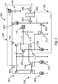
- FIGS 3 and 4 show a circuit 200 for a mobile communications device of the kind shown in Figure 1 , in accordance with an embodiment of this disclosure.
- the circuit 200 in Figures 3 and 4 incorporates features implementing the current control circuit 130 shown in Figure 2 , as well as the transistor 128, the power supply rail 110, and SIMVCC 116.
- the circuit 200 includes a first switch 228 and a second switch 214, which are used to implement the current control function as the transistor 128 is being switched on.
- the switching on of the transistor 128 may comprise two main stages.
- Figure 3 shows the circuit 200 with the first switch 228 and the second switch 214 configured for the first stage
- Figure 4 shows the circuit 200 with the first switch 228 and the second switch 214 configured for the second stage.
- the circuit 200 includes a first transistor 128, which corresponds to the transistor 128 described above in relation to Figure 2 .
- the circuit 200 also includes a second transistor 204, a third transistor 210 and a fourth transistor 208.
- the transistors 128, 204, 208, 210 may each be a p-type MOSFET, although this is not essential, and other kinds of transistor may be used instead.
- each transistor 128, 204, 208, 210 will be of the same type (i.e. p-type or n-type).
- the circuit 200 also includes a first switch 228 and a second switch 214.
- Each switch 228, 214 may be implemented using a transistor.
- Each transistor 128, 204, 208, 210 may be implemented using a MISFET (e.g. a MOSFET). Any suitable kind of MISFET may be chosen (e.g. enhancement/depletion mode transistors may used).
- a gate of the first transistor 128 is coupleable to reference potential via the second switch 214. When the second switch is closed, the gate of the first transistor 128 is connected to the reference potential, which may be chosen such that the closing of the second switch 214 causes the first transistor 128 to be fully switched on.
- the reference potential may, for instance be ground.
- the second transistor 204 has a gate coupleable to the gate of the first transistor 128 via the first switch 228. Accordingly, the gates of the first transistor 128 and the second transistor 204 may be selectively coupled and decoupled by closing and opening the first switch 228.
- the gates of the third transistor 210 and a fourth transistor 208 are coupled together.
- the second transistor 204 and the fourth transistor 208 are coupled in series between the power supply rail 110 and a first current source 222.
- the first transistor 128 and the third transistor 210 are coupled in series between the power supply rail 110 and a second current source 224.
- Each current source 222, 224 provides a reference current (I1, I2).
- a node located between the fourth transistor 208 and the first current source 222 is coupled to a node located between the gate of the second transistor 204 and the first switch 228.
- a node located between the third transistor 210 and the second current source 224 is coupled to the gates of the third transistor 210 and fourth transistor 208.
- first switch 228 In the first stage of switching on the first transistor 128, the first switch 228 is closed and the second switch 214 is open (as shown in Figure 3 ). In the second stage of switching on the first transistor 128, the first switch 228 is open and the second switch 214 is closed (as shown in Figure 4 ).
- the switches 228, 214 are controlled by the current control circuit 130 using control signals.
- a first control signal 240 (SW_DIS) is used to open and close the first switch 228 and a second control signal 230 (SW_EN) is used to open and close the second switch 214.
- the circuit 200 may be provided with further features for generating the first control signal 240 and the second control signal 230. These will now be described below.
- the current control circuit may further comprise a fifth transistor 206.
- the fifth transistor 206 may be coupled in series with the first transistor 128 and a third current source 226.
- the third current source 226 provides a reference current (13).
- the fifth transistor 206 may be implemented using a MISFET (e.g. a MOSFET). Any suitable kind of MISFET may be chosen (e.g. enhancement/depletion mode transistors may used).
- the fifth transistor 206 is the same type (i.e. p-type or n-type) as the first transistor 128.
- the fifth transistor 206 may have a gate that is coupled to a node located between the first switch 228 and the gate of the first transistor 128.
- the fifth transistor 206 may also have a first current terminal (the source in this example) coupled to a node located between the first transistor 128 and a power supply output of the near field communications integrated circuit 14.
- the power supply output of the near field communications integrated circuit 14 is represented in Figures 3 and 4 as SIMVCC 116.
- the fifth transistor 206 may also have a second current terminal (the drain in this example) coupled to the third current source 226.
- the current control circuit 130 may be operable to produce first control signal 240 and the second control signal 230 dependent upon a current at the second current terminal of the fifth transistor 206.
- the current control circuit 130 may further include a sixth transistor 212 and a seventh transistor 220.
- the sixth transistor 212 and the seventh transistor 220 form a current mirror. As shown in Figures 3 and 4 , to implement the current mirror:
- the input of the current mirror is coupled to a node located between the second current terminal of the firth transistor 206 and the third current source 226.
- the input of the current mirror measures a difference between the current at the second current terminal of the firth transistor 206 and the reference current provided by third current source 226.
- the current at the output of the current mirror is governed by this difference.
- the output of the current mirror may be coupled to the power supply rail 110 via a fourth current source 227.
- the fourth current source 227 provides a reference current (14).
- the current control circuit is operable to use the output of the current mirror to produce the first control signal 240 and the second control signal 230.
- the current control circuit 130 may further include a latch 250.
- the latch 250 may have an input that is coupled to the output of the current mirror.
- An inverter 242 may be coupled between the input of the latch 250 and the output of the current mirror. Accordingly, the output of the current mirror may be used to set/reset the latch 250.
- the latch 250 may also have an output.
- the output of the latch 250 may be coupled to the first switch 228 via an inverter 244. This can allow the latch 250 and inverter 244 to produce the first control signal 240 and supply it to first switch 228.
- the output of the latch 250 may also be coupled to the second switch 214. This can allow the latch 250 to produce the second control signal 230 and supply it to second switch 214. Note that when the output of the latch 250 is low, the first control signal 240 is high, whereby the first switch 228 is closed, and second control signal 230 is low, whereby the second switch 214 is open (see Figure 3 ). Conversely, when the output of the latch 250 is high, the first control signal 240 is low, whereby the first switch 228 is open, and second control signal 230 is high, whereby the second switch 214 is closed (see Figure 4 ).
- the switching on of the first transistor 128 may be implemented in two stages. In the first stage:
- the current I load (see Figure 3 ) is initially associated with loading the external capacitance CSIMCC 118 on the universal integrated circuit card supply SIMVCC 116.
- I load may be fixed by the first current source 222 (which provides the first reference current I1) and the ratio of the first transistor 128 to the second transistor 204.
- the third transistor 210 and the fourth transistor 208 can ensure that the drain to source voltage Vds of the first transistor 128 copies to the second transistor 204.
- the third transistor 210 and the fourth transistor 208 may be substantially matched, to obtain the same drain voltage on the first transistor 128 and the second transistor 204, thereby to allow a good copy of V ds to be made in this way.
- SIMVCC 116 is low. Accordingly, the gate to source voltage V gs of the fifth transistor 206 is greater than zero. Because of this the second current terminal of the fifth transistor 206, and consequently the input to the current mirror remain low. Therefore, the first control signal 240 remains high and the second control signal 230 remains low.
- the voltage at SIMVCC 116 will begin to rise. Consequently, the fifth transistor 206 will, at some point, begin to conduct. As the voltage at SIMVCC 116 continues to rise, the current in the fifth transistor 206 will eventually exceed the reference current (13) provided by the third current source 226. Because of this, current will begin to flow into input of the current mirror (in this example, the sixth transistor 212 begins to conduct), which in turn will pull down the output (COMP_OUT) of the current mirror. This pulling down of the output (COMP_OUT) of the current mirror will, via the inverter 242, cause the latch 250 to be set, initiating the second stage of the switching on of the first transistor 128.
- the setting of the latch 250 changes the state of the first control signal 240 (via the inverter 244) from high to low and the second control signal 230 changes state from low to high.
- This causes the first switch 128 to open, which decouples the gate of the first transistor 128 from the gate of the second transistor 204.
- This also causes the second switch 214 to close which couples the gate of the first transistor 128 to a reference voltage (e.g. ground), which causes the first transistor 128 to be fully switched on, allowing the first transistor 128 to provide a (e.g. low ohmic, compliant with the ETSI standard (1.62V @ 10ma)) path to pass current from the power supply rail 110 to SIMVCC 116.
- a reference voltage e.g. ground
- the reference current (13) provided by the third current source 226 may be chosen such that the second current terminal of the sixth transistor 212 and accordingly the input (CHECK) of the current mirror, goes high once this voltage condition is reached.
- the first transistor 128 and the second transistor 204 may be substantially matched. This can allow a copy of the reference current I1 to be obtained, in order to limit the current I load in the first stage.
- the first transistor 128 and the fifth transistor 206 may be substantially matched. This can allow the fifth transistor 206 to be used accurately to detect desaturation in the first transistor 128.
- the ratio between the first transistor 128 and the second transistor 204 may be substantially the same as the ratio between the third transistor 210 and the fourth transistor 208, as well as the ratio between the reference currents (I1, I2) provided by the first current source 222 and the second current source 224.
- the integrated circuit includes a power supply rail for providing a regulated supply of power to components within the integrated circuit.
- the integrated circuit also includes a first transistor coupled between the power supply rail and a power supply output of the integrated circuit for selectively providing power to a universal integrated circuit card (UICC) of the mobile communications device from the power supply rail while the mobile communications device is in an off state.
- the integrated circuit further includes a current control circuit for controlling the operation of the first transistor to prevent a drop in voltage on the power supply rail as the first transistor is switched to an on state to couple the power supply rail to the power supply output.
Landscapes
- Engineering & Computer Science (AREA)
- Physics & Mathematics (AREA)
- Electromagnetism (AREA)
- General Physics & Mathematics (AREA)
- Radar, Positioning & Navigation (AREA)
- Automation & Control Theory (AREA)
- Computer Networks & Wireless Communication (AREA)
- Signal Processing (AREA)
- Semiconductor Integrated Circuits (AREA)
- Electronic Switches (AREA)
Abstract
Description
- The present specification relates to a near field communications (NFC) integrated circuit for a mobile communications device. The present specification also relates to a mobile communications device including the near field communications (NFC) integrated circuit. The present specification further relates to a method of operating a mobile communications device.
- In an OFF state of a mobile communications device such as a mobile phone, the Universal Integrated Circuit Card (UICC) is not directly supplied by the mobile communications device platform. A Near Field Communications (NFC) chip of the mobile communications device may therefore need to use an internal regulator to supply the UICC in order to perform secure transactions.
- In order to reduce current consumption, a simple switch may be used to supply the external UICC from an internal regulator, such as a central supply of the NFC chip. This solution may generally only be used when the mobile communications device is in its OFF state, in which case the external UICC does not get any supply from phone platform. The switch may be low ohmic in order to provide a supply that is compliant with the ETSI standard (1.62V @ 10ma).
- Aspects of the present disclosure are set out in the accompanying independent and dependent claims. Combinations of features from the dependent claims may be combined with features of the independent claims as appropriate and not merely as explicitly set out in the claims.
- According to an aspect of the present disclosure, there is provided a near field communications (NFC) integrated circuit for a mobile communications device, the integrated circuit comprising:
- a power supply rail for providing a regulated supply of power to components within the integrated circuit;
- a first transistor coupled between the power supply rail and a power supply output of the integrated circuit for selectively providing power to a universal integrated circuit card (UICC) of the mobile communications device from the power supply rail while the mobile communications device is in an off state; and
- a current control circuit for controlling the operation of the first transistor to prevent a drop in voltage on the power supply rail as the first transistor is switched to an on state to couple the power supply rail to the power supply output.
- According to another aspect of the present disclosure, there is provided a method of operating a mobile communications device, the method comprising:
- a power supply rail providing a regulated supply of power to components within a near field communications (NFC) integrated circuit of the mobile communications device;
- a first transistor coupled between the power supply rail and a power supply output of the integrated circuit selectively providing power to a universal integrated circuit card (UICC) of the mobile communications device from the power supply rail while the mobile communications device is in an off state; and
- a current control circuit controlling the operation of the first transistor to prevent a drop in voltage on the power supply rail as the first transistor is switched to an on state to couple the power supply rail to the power supply output.
- The provision of the current control circuit can protect components of the near field communications integrated circuit against a current peak that may be drawn to load an external capacitance on the universal integrated circuit card supply, leading to a drop in voltage on the power supply rail as the first transistor is switched to an on state to couple the power supply rail to the power supply output. This drop in voltage may otherwise cause a reset of the near field communications integrated circuit, or other functionality problems relating to the operation of the internal components of the near field communications integrated circuit, which are also supplied from the power supply rail.
- In one embodiment, the current control circuit may include a first switch; a second switch, wherein a gate of the first transistor is coupleable to reference potential via the second switch; a second transistor having a gate coupleable to the gate of the first transistor via the first switch, and a third transistor and a fourth transistor, wherein a gate of the third transistor is coupled to a gate of the fourth transistor. The second transistor and the fourth transistor may be coupled in series between the power supply rail and a first current source. The first transistor and the third transistor may be coupled in series between the power supply rail and a second current source. A node located between the fourth transistor and the first current source may be coupled to a node located between the gate of the second transistor and the first switch. A node located between the third transistor and the second current source may be coupled to the gates of the third transistor and fourth transistor.
- The current control circuit may be operable in an initial step for switching the first transistor to the on state to close the first switch and to open the second switch. In this way, current flow from the power supply rail to the power supply output may be governed by a ratio of currents flowing through the first transistor and the second transistor. This can allow current to be drawn to load the external capacitance on the universal integrated circuit card supply without leading to a drop in voltage on the power supply rail in the initial step.
- The current control circuit may be operable in a next step for switching the first transistor to the on state to open the first switch and to close the second switch. The first transistor may thus be fully switched to its on state to provide power from the power supply rail to the power supply output. As the voltage at the power supply output rises, the first transistor may subsequently (i.e. in the next step) be fully switched on (by operating the first and second switches using the control signals) without leading to the aforementioned drop in voltage on the power supply rail.
- In one embodiment, the current control circuit may further include a fifth transistor coupled in series with the first transistor and a third current source. The fifth transistor may have a gate coupled to a node located between the first switch and the gate of the first transistor. The fifth transistor may also have a first current terminal coupled to a node located between the first transistor and the power supply output. The fifth transistor may further have a second current terminal coupled to said third current source. The current control circuit may be operable to produce control signals for operating the first switch and the second switch dependent upon a current at the second current terminal. The fifth transistor may thus be used to determine the appropriate time at which the first transistor may be fully switched on without leading to the aforementioned drop in voltage on the power supply rail. For instance, this may be done by determining whether the current at the second current terminal of the fifth transistor exceeds a reference current provided by the third current source.
- In one embodiment, the current control circuit may further include a sixth transistor and a seventh transistor forming a current mirror. An input of the current mirror may be coupled to a node located between the second current terminal of the firth transistor and the third current source. The current control circuit may be operable to use an output of the current mirror to produce the control signals. The input of the current mirror may for instance receive a current determined by the difference between the current at the second current terminal of the firth transistor and the reference current provided by the third current source. This can allow the current mirror to determine when the current at the second current terminal of the firth transistor exceeds the reference current provided by the third current source, for generating the appropriate control signals for the first and second switches.
- In one embodiment, the current control circuit may further include a latch. The latch may have an input coupled to the output of the current mirror. The latch may have an output. The output of the latch may be coupled to the first switch via an inverter, for providing a first the control signal to the second switch. The output of the latch may also be coupled to the second switch for providing a second said control signal to the second switch. The output of the current mirror may thus be used to program the latch, and the output of the latch may be used to produce the control signals for operating the first switch and the second switch.
- Some of the transistors of the current control circuit may be matched. Matching the transistors involves providing substantially equally sized transistors so that the same current flows through each transistor when substantially the same voltages are applied to the terminals of the transistors.
- For instance the first and fifth transistors may be substantially matched. This can allow the fifth transistor to be used accurately to detect desaturation in the first transistor.
- In another embodiment, the first and second transistors may be substantially matched. This can allow the desired load current Iload to flow to the power supply output. In particular, this can allow a copy of the reference current I1 to be obtained, in order to limit Iload as the first transistor is being switched to its on state.
- In a further embodiment, the third and fourth transistors may be substantially matched. This can allow the same drain voltage to be obtained on the first transistor and the second transistor.
- According to another aspect of the present disclosure, there is provided a mobile communications device including the near field communications (NFC) integrated circuit of any of claims 1 to 10.
- The mobile communications device may, further include the universal integrated circuit card (UICC).
- The mobile communications device may be operable to provide power to the universal integrated circuit card without providing power to the universal integrated circuit card from the near field communications (NFC) integrated circuit when the mobile communications device is in an on state
- Embodiments of this disclosure will be described hereinafter, by way of example only, with reference to the accompanying drawings in which like reference signs relate to like elements and in which:
-
Figure 1 shows a mobile communications device in accordance with an embodiment of this disclosure; -
Figure 2 shows a circuit for a mobile communications device of the kind shown inFigure 1 , in accordance with an embodiment of this disclosure; and -
Figures 3 and4 show a circuit for a mobile communications device of the kind shown inFigure 1 , in accordance with and embodiment of this disclosure. - Embodiments of this disclosure are described in the following with reference to the accompanying drawings.
-
Figure 1 shows amobile communications device 10 in accordance with an embodiment of this disclosure. Themobile communications device 10 may for instance be a mobile phone, or any other device incorporating a universal integrated circuit card (UICC) and having near field communications (NFC) functionality. - The
mobile communications device 10 may include ahousing 2, adisplay 4 and one or more user input devices, such as button(s) 6. - The
mobile communications device 10 includes a universalintegrated circuit card 20. Thehousing 2 may include an opening 8, to allow the universalintegrated circuit card 20 to be installed. - The
housing 2 may contain abattery 12 for powering themobile communications device 10. - The
mobile communications device 10 includes a near field communications (NFC) integratedcircuit 14. The near field communications integratedcircuit 14 may located inside thehousing 2. The near field communications integratedcircuit 14 may provide functionality such as secure payment functionality for themobile communications device 10. This functionality may involve the use of the universalintegrated circuit card 20. While themobile communications device 10 is switched on, thebattery 12 may be used to provide power to the universalintegrated circuit card 20 via the main internal power supply of themobile communications device 10. This can allow themobile communications device 10 to connect with a cellular network, and can also power the universalintegrated circuit card 20 during provision of the aforementioned near field communications functionality. - When the
mobile communications device 10 is switched off, power cannot be provided directly from the main internal power supply of themobile communications device 10 to the universalintegrated circuit card 20. In accordance with embodiments of this disclosure, to provide near field communications functionality while themobile communications device 10 is switched off, the near field communications integratedcircuit 14 may provide power to the universalintegrated circuit card 20, when near field communications functions are required. -
Figure 2 shows acircuit 100 for a mobile communications device of the kind shown inFigure 1 , in accordance with an embodiment of this disclosure. - In
Figure 2 ,VBAT 102 represents the power supply received by the near field communications integratedcircuit 14. This power supply may be regulated by aninternal regulator 104 of the near field communications integratedcircuit 14, e.g. using atransistor 106. The regulated power provided by theinternal regulator 104 may be provided to a power supply rail 110 (VDD) of the near field communications integratedcircuit 14. Thepower supply rail 110 may be used to provide regulated power to components (e.g. a processor, memory etc.) of the near field communications integratedcircuit 14. Thepower supply rail 110 may have an internal orexternal capacitance CVDD 108. Thepower supply rail 110 may, for instance, operate at 1.8V. -
SIMVCC 116 represents the power supply to the universalintegrated circuit card 20 of themobile communications device 10. TheSIMVCC 116 may, for instance, be a power supply pin for the universalintegrated circuit card 20.SIMVCC 116 has anexternal capacitance CSIMVCC 118. -
PMUVCC 112 represents the main internal power supply of the mobile communications device 10 (which may be provided by a power management unit of the mobile communications device 10). When themobile communications device 10 is switched on, acontrol signal 122 may be asserted to switch ontransistor 114, for providing power toSIMVCC 116 fromPMUVCC 122. When themobile communications device 10 is switched off, thecontrol signal 122 may be de-asserted. Additionally, acontrol signal 126 may be asserted to switch ontransistor 120, to connectSIMVCC 116 to ground, thereby to ensure that no power is provided toSIMVCC 116. - As noted above, when the
mobile communications device 10 is switched off, the near field communications integratedcircuit 14 may provide power to the universal integrated circuit card 20 - this may be implemented by coupling thepower supply rail 110 toSIMVCC 116. When near field communications functionality is required with themobile communications device 10 switched off,control signal 124 may be asserted for switching ontransistor 128, thereby to provide a path from thepower supply rail 110 toSIMVCC 116.Control signal 126 may also be de-asserted, to switch offtransistor 120, thereby to disconnectSIMVCC 116 from ground. - If
transistor 128 were to be fully switched on immediately, this may give rise to the aforementioned current peak that may be drawn to load anexternal capacitance CSIMCC 118 on the universal integrated circuit card supply. This may in turn lead to a drop in voltage on thepower supply rail 110 as thetransistor 128 is switched on. This drop in voltage may cause a reset of the near field communications integratedcircuit 14, or other functionality problems relating to the operation of the internal components (e.g. a processor, memory etc.) of the near field communications integratedcircuit 14, which are also supplied from thepower supply rail 110. - The
transistor 128 may typically be low ohmic (that is to say that thetransistor 128 has a low on state resistance Ron), so that the power supply provided to the universalintegrated circuit card 20 by the near field communications integratedcircuit 14 with minimal losses (e.g. to comply with the ETSI standard (1.62V @ 10mA). The low on state resistance Ron of thetransistor 128 may exacerbate the above mentioned problem relating to the current peak that may be drawn to load an external capacitance on the universal integrated circuit card supply. - In order to address this problem, in accordance with embodiments of this disclosure, the near field communications integrated
circuit 14 is provided with acurrent control circuit 130. Thecurrent control circuit 130 may operate to manage the switching on of thetransistor 128. In particular, thecurrent control circuit 130 may operate to limit the flow of current from thepower supply rail 110 toSIMVCC 116, until it is safe to fully turn on thetransistor 128 without causing a voltage drop on thepower supply rail 110. -
Figures 3 and4 show acircuit 200 for a mobile communications device of the kind shown inFigure 1 , in accordance with an embodiment of this disclosure. Thecircuit 200 inFigures 3 and4 incorporates features implementing thecurrent control circuit 130 shown inFigure 2 , as well as thetransistor 128, thepower supply rail 110, andSIMVCC 116. - As will be described below, the
circuit 200 includes afirst switch 228 and asecond switch 214, which are used to implement the current control function as thetransistor 128 is being switched on. The switching on of thetransistor 128 may comprise two main stages.Figure 3 shows thecircuit 200 with thefirst switch 228 and thesecond switch 214 configured for the first stage, whileFigure 4 shows thecircuit 200 with thefirst switch 228 and thesecond switch 214 configured for the second stage. - In this embodiment, the
circuit 200 includes afirst transistor 128, which corresponds to thetransistor 128 described above in relation toFigure 2 . Thecircuit 200 also includes asecond transistor 204, athird transistor 210 and afourth transistor 208. Thetransistors transistor - As noted above, the
circuit 200 also includes afirst switch 228 and asecond switch 214. Eachswitch - The connections of the above noted features of the
circuit 200 will now be described. - Each
transistor Figure 3 , in this embodiment, a gate of thefirst transistor 128 is coupleable to reference potential via thesecond switch 214. When the second switch is closed, the gate of thefirst transistor 128 is connected to the reference potential, which may be chosen such that the closing of thesecond switch 214 causes thefirst transistor 128 to be fully switched on. The reference potential may, for instance be ground. - The
second transistor 204 has a gate coupleable to the gate of thefirst transistor 128 via thefirst switch 228. Accordingly, the gates of thefirst transistor 128 and thesecond transistor 204 may be selectively coupled and decoupled by closing and opening thefirst switch 228. - The gates of the
third transistor 210 and afourth transistor 208 are coupled together. - The
second transistor 204 and thefourth transistor 208 are coupled in series between thepower supply rail 110 and a firstcurrent source 222. Thefirst transistor 128 and thethird transistor 210 are coupled in series between thepower supply rail 110 and a secondcurrent source 224. Eachcurrent source - A node located between the
fourth transistor 208 and the firstcurrent source 222 is coupled to a node located between the gate of thesecond transistor 204 and thefirst switch 228. A node located between thethird transistor 210 and the secondcurrent source 224 is coupled to the gates of thethird transistor 210 andfourth transistor 208. - In the first stage of switching on the
first transistor 128, thefirst switch 228 is closed and thesecond switch 214 is open (as shown inFigure 3 ). In the second stage of switching on thefirst transistor 128, thefirst switch 228 is open and thesecond switch 214 is closed (as shown inFigure 4 ). Theswitches current control circuit 130 using control signals. In particular, a first control signal 240 (SW_DIS) is used to open and close thefirst switch 228 and a second control signal 230 (SW_EN) is used to open and close thesecond switch 214. - The
circuit 200 may be provided with further features for generating thefirst control signal 240 and thesecond control signal 230. These will now be described below. - The current control circuit may further comprise a
fifth transistor 206. Thefifth transistor 206 may be coupled in series with thefirst transistor 128 and a thirdcurrent source 226. The thirdcurrent source 226 provides a reference current (13). Thefifth transistor 206 may be implemented using a MISFET (e.g. a MOSFET). Any suitable kind of MISFET may be chosen (e.g. enhancement/depletion mode transistors may used). Typically, thefifth transistor 206 is the same type (i.e. p-type or n-type) as thefirst transistor 128. - The
fifth transistor 206 may have a gate that is coupled to a node located between thefirst switch 228 and the gate of thefirst transistor 128. Thefifth transistor 206 may also have a first current terminal (the source in this example) coupled to a node located between thefirst transistor 128 and a power supply output of the near field communications integratedcircuit 14. In the present example, the power supply output of the near field communications integratedcircuit 14 is represented inFigures 3 and4 asSIMVCC 116. Thefifth transistor 206 may also have a second current terminal (the drain in this example) coupled to the thirdcurrent source 226. In accordance with embodiments of this disclosure, and as will be described below, thecurrent control circuit 130 may be operable to producefirst control signal 240 and thesecond control signal 230 dependent upon a current at the second current terminal of thefifth transistor 206. - The
current control circuit 130 may further include asixth transistor 212 and aseventh transistor 220. Thesixth transistor 212 and theseventh transistor 220 form a current mirror. As shown inFigures 3 and4 , to implement the current mirror: - the gates of the
sixth transistor 212 and theseventh transistor 220 may be connected together; - a first current terminal (the source, in this example) of the each
transistor - the gates of the
sixth transistor 212 and theseventh transistor 220 are also connected to a second current terminal (the drain in this example) of thesixth transistor 212. - The input of the current mirror is coupled to a node located between the second current terminal of the
firth transistor 206 and the thirdcurrent source 226. The input of the current mirror measures a difference between the current at the second current terminal of thefirth transistor 206 and the reference current provided by thirdcurrent source 226. The current at the output of the current mirror is governed by this difference. - The output of the current mirror may be coupled to the
power supply rail 110 via a fourthcurrent source 227. The fourthcurrent source 227 provides a reference current (14). - The current control circuit is operable to use the output of the current mirror to produce the
first control signal 240 and thesecond control signal 230. To implement this, thecurrent control circuit 130 may further include alatch 250. Thelatch 250 may have an input that is coupled to the output of the current mirror. Aninverter 242 may be coupled between the input of thelatch 250 and the output of the current mirror. Accordingly, the output of the current mirror may be used to set/reset thelatch 250. - The
latch 250 may also have an output. The output of thelatch 250 may be coupled to thefirst switch 228 via aninverter 244. This can allow thelatch 250 andinverter 244 to produce thefirst control signal 240 and supply it tofirst switch 228. The output of thelatch 250 may also be coupled to thesecond switch 214. This can allow thelatch 250 to produce thesecond control signal 230 and supply it tosecond switch 214. Note that when the output of thelatch 250 is low, thefirst control signal 240 is high, whereby thefirst switch 228 is closed, andsecond control signal 230 is low, whereby thesecond switch 214 is open (seeFigure 3 ). Conversely, when the output of thelatch 250 is high, thefirst control signal 240 is low, whereby thefirst switch 228 is open, andsecond control signal 230 is high, whereby thesecond switch 214 is closed (seeFigure 4 ). - The operation of the
current control circuit 130 will now be described, with reference to thecircuit 200 shown inFigures 3 and4 . - As stated previously, the switching on of the
first transistor 128 may be implemented in two stages. In the first stage: - the
first control signal 240 is high (due to the reference current provided by the fourth current source 227), hence thefirst switch 228 is closed; - the
second control signal 230 is low, hence thesecond switch 214 is open; - the second current terminal of the sixth transistor 212 (and consequently the input of the current mirror) is low, due to the reference current (13) provided by the third
current source 226; and - the output of the current mirror is low, due to the reference current (14) provided by the fourth
current source 227. - As the near field communications integrated
circuit 14 begins to provide power from thepower supply rail 110 to the power supply output, the current Iload (seeFigure 3 ) is initially associated with loading theexternal capacitance CSIMCC 118 on the universal integrated circuitcard supply SIMVCC 116. - In accordance with embodiments of this disclosure, Iload may be fixed by the first current source 222 (which provides the first reference current I1) and the ratio of the
first transistor 128 to thesecond transistor 204. Note that thethird transistor 210 and thefourth transistor 208 can ensure that the drain to source voltage Vds of thefirst transistor 128 copies to thesecond transistor 204. In accordance with embodiments of this disclosure, thethird transistor 210 and thefourth transistor 208 may be substantially matched, to obtain the same drain voltage on thefirst transistor 128 and thesecond transistor 204, thereby to allow a good copy of Vds to be made in this way. - Initially,
SIMVCC 116 is low. Accordingly, the gate to source voltage Vgs of thefifth transistor 206 is greater than zero. Because of this the second current terminal of thefifth transistor 206, and consequently the input to the current mirror remain low. Therefore, thefirst control signal 240 remains high and thesecond control signal 230 remains low. - As the
external capacitance CSIMVCC 118 ofSIMVCC 116 becomes loaded, the voltage atSIMVCC 116 will begin to rise. Consequently, thefifth transistor 206 will, at some point, begin to conduct. As the voltage atSIMVCC 116 continues to rise, the current in thefifth transistor 206 will eventually exceed the reference current (13) provided by the thirdcurrent source 226. Because of this, current will begin to flow into input of the current mirror (in this example, thesixth transistor 212 begins to conduct), which in turn will pull down the output (COMP_OUT) of the current mirror. This pulling down of the output (COMP_OUT) of the current mirror will, via theinverter 242, cause thelatch 250 to be set, initiating the second stage of the switching on of thefirst transistor 128. - The setting of the
latch 250 changes the state of the first control signal 240 (via the inverter 244) from high to low and the second control signal 230 changes state from low to high. This causes thefirst switch 128 to open, which decouples the gate of thefirst transistor 128 from the gate of thesecond transistor 204. This also causes thesecond switch 214 to close which couples the gate of thefirst transistor 128 to a reference voltage (e.g. ground), which causes thefirst transistor 128 to be fully switched on, allowing thefirst transistor 128 to provide a (e.g. low ohmic, compliant with the ETSI standard (1.62V @ 10ma)) path to pass current from thepower supply rail 110 toSIMVCC 116. - The
fifth transistor 206 may thus be used to detect desaturation in thefirst transistor 128. Because the gate of thefifth transistor 206 is coupled to a node located between thefirst switch 228 and the gate of thefirst transistor 128, thefifth transistor 206 and thefirst transistor 128 both have the same gate voltage. Accordingly, when the voltage atSIMVCC 116 rises to SIMVCC = VDDNV - Vdrop (where VDDNV is the internal low drop out (LDO) voltage and Vdrop is the voltage drop across thefirst transistor 128, which is defined by the on state resistance of the first transistor 128), the gate to source voltage Vgs of thefirst transistor 128 will be slightly lower than the gate to source voltage Vgs of thefifth transistor 206. The reference current (13) provided by the thirdcurrent source 226 may be chosen such that the second current terminal of thesixth transistor 212 and accordingly the input (CHECK) of the current mirror, goes high once this voltage condition is reached. - In accordance with embodiments of this disclosure, the
first transistor 128 and thesecond transistor 204 may be substantially matched. This can allow a copy of the reference current I1 to be obtained, in order to limit the current Iload in the first stage. - In accordance with embodiments of this disclosure, the
first transistor 128 and thefifth transistor 206 may be substantially matched. This can allow thefifth transistor 206 to be used accurately to detect desaturation in thefirst transistor 128. - Moreover, in accordance with embodiments of this disclosure, the ratio between the
first transistor 128 and thesecond transistor 204 may be substantially the same as the ratio between thethird transistor 210 and thefourth transistor 208, as well as the ratio between the reference currents (I1, I2) provided by the firstcurrent source 222 and the secondcurrent source 224. - Accordingly, there has been described a near field communications (NFC) integrated circuit and method for a mobile communications device. The integrated circuit includes a power supply rail for providing a regulated supply of power to components within the integrated circuit. The integrated circuit also includes a first transistor coupled between the power supply rail and a power supply output of the integrated circuit for selectively providing power to a universal integrated circuit card (UICC) of the mobile communications device from the power supply rail while the mobile communications device is in an off state. The integrated circuit further includes a current control circuit for controlling the operation of the first transistor to prevent a drop in voltage on the power supply rail as the first transistor is switched to an on state to couple the power supply rail to the power supply output.
- Although particular embodiments of this disclosure have been described, it will be appreciated that many modifications/additions and/or substitutions may be made within the scope of the claims.
Claims (15)
- A near field communications (NFC) integrated circuit for a mobile communications device, the integrated circuit comprising:a power supply rail for providing a regulated supply of power to components within the integrated circuit;a first transistor coupled between the power supply rail and a power supply output of the integrated circuit for selectively providing power to a universal integrated circuit card (UICC) of the mobile communications device from the power supply rail while the mobile communications device is in an off state; anda current control circuit for controlling the operation of the first transistor to prevent a drop in voltage on the power supply rail as the first transistor is switched to an on state to couple the power supply rail to the power supply output.
- The integrated circuit of claim 1, wherein the current control circuit comprises:a first switch;a second switch, wherein a gate of the first transistor is coupleable to reference potential via the second switch;a second transistor having a gate coupleable to the gate of the first transistor via the first switch, anda third transistor and a fourth transistor, wherein a gate of the third transistor is coupled to a gate of the fourth transistor,wherein the second transistor and the fourth transistor are coupled in series between the power supply rail and a first current source,wherein the first transistor and the third transistor are coupled in series between the power supply rail and a second current source,wherein a node located between the fourth transistor and the first current source is coupled to a node located between the gate of the second transistor and the first switch, andwherein a node located between the third transistor and the second current source is coupled to the gates of the third transistor and fourth transistor.
- The integrated circuit of claim 2, wherein the current control circuit is operable in an initial step for switching the first transistor to the on state to close the first switch and to open the second switch, whereby current flow from the power supply rail to the power supply output is governed by a ratio of currents flowing through the first transistor and the second transistor.
- The integrated circuit of claim 3, wherein the current control circuit is operable in a next step for switching the first transistor to the on state to open the first switch and to close the second switch, whereby the first transistor is fully switched to said on state to provide power from the power supply rail to the power supply output.
- The integrated circuit of any of claims 2 to 4, wherein the current control circuit further comprises a fifth transistor coupled in series with the first transistor and a third current source, the fifth transistor having:a gate coupled to a node located between the first switch and the gate of the first transistor;a first current terminal coupled to a node located between the first transistor and the power supply output; anda second current terminal coupled to said third current source,wherein the current control circuit is operable to produce control signals for operating the first switch and the second switch dependent upon a current at said second current terminal.
- The integrated circuit of claim 5, wherein the current control circuit further comprises a sixth transistor and a seventh transistor forming a current mirror, wherein:an input of the current mirror is coupled to a node located between the second current terminal of the firth transistor and the third current source;and wherein the current control circuit is operable to use an output of the current mirror to produce said control signals.
- The integrated circuit of claim 6, wherein the current control circuit further comprises a latch having:an input coupled to the output of the current mirror; andan output coupled to:the first switch via an inverter, for providing a first said control signal to the second switch; andthe second switch for providing a second said control signal to the second switch.
- The integrated circuit of any of claims 5 to 7, wherein the first and fifth transistors are substantially matched.
- The integrated circuit of any of claims 2 to 8, wherein the first and second transistors are substantially matched.
- The integrated circuit of any of claims 2 to 9, wherein the third and fourth transistors are substantially matched.
- A mobile communications device including the near field communications (NFC) integrated circuit of any preceding claim.
- The mobile communications device of claim 11, further comprising said universal integrated circuit card (UICC).
- The mobile communications device of claim 12, wherein the mobile communications device is operable to provide power to the universal integrated circuit card without providing power to the universal integrated circuit card from the near field communications (NFC) integrated circuit when the mobile communications device is in an on state.
- A method of operating a mobile communications device, the method comprising:a power supply rail providing a regulated supply of power to components within a near field communications (NFC) integrated circuit of the mobile communications device;a first transistor coupled between the power supply rail and a power supply output of the integrated circuit selectively providing power to a universal integrated circuit card (UICC) of the mobile communications device from the power supply rail while the mobile communications device is in an off state; anda current control circuit controlling the operation of the first transistor to prevent a drop in voltage on the power supply rail as the first transistor is switched to an on state to couple the power supply rail to the power supply output.
- The method of claim 15, further comprising the mobile communications device providing power to the universal integrated circuit card without providing power to the universal integrated circuit card from the near field communications (NFC) integrated circuit when the mobile communications device is in an on state.
Priority Applications (2)
| Application Number | Priority Date | Filing Date | Title |
|---|---|---|---|
| EP19305792.4A EP3754848B1 (en) | 2019-06-20 | 2019-06-20 | Near field communications ic and method for mobile communications device |
| CN202010499802.7A CN112118032B (en) | 2019-06-20 | 2020-06-04 | Near field communication integrated circuit for mobile communication device, mobile communication device and operation method thereof |
Applications Claiming Priority (1)
| Application Number | Priority Date | Filing Date | Title |
|---|---|---|---|
| EP19305792.4A EP3754848B1 (en) | 2019-06-20 | 2019-06-20 | Near field communications ic and method for mobile communications device |
Publications (2)
| Publication Number | Publication Date |
|---|---|
| EP3754848A1 true EP3754848A1 (en) | 2020-12-23 |
| EP3754848B1 EP3754848B1 (en) | 2023-11-15 |
Family
ID=67253835
Family Applications (1)
| Application Number | Title | Priority Date | Filing Date |
|---|---|---|---|
| EP19305792.4A Active EP3754848B1 (en) | 2019-06-20 | 2019-06-20 | Near field communications ic and method for mobile communications device |
Country Status (2)
| Country | Link |
|---|---|
| EP (1) | EP3754848B1 (en) |
| CN (1) | CN112118032B (en) |
Citations (4)
| Publication number | Priority date | Publication date | Assignee | Title |
|---|---|---|---|---|
| EP2450835A2 (en) * | 2010-10-28 | 2012-05-09 | Renesas Electronics Corporation | Semiconductor device for wireless communication |
| US20130169059A1 (en) * | 2011-11-22 | 2013-07-04 | Fairchild Semiconductor Corporation | Dual Input Single Output Power Multiplexer for Near Field Communication Application |
| EP2738671A1 (en) * | 2012-12-03 | 2014-06-04 | Nxp B.V. | Method and system for controlling operations in a mobile communication device that is enabled for near field communication (NFC) |
| EP3258611A1 (en) * | 2015-05-15 | 2017-12-20 | Huawei Technologies Co., Ltd. | Mobile device having near field wireless communication function |
Family Cites Families (3)
| Publication number | Priority date | Publication date | Assignee | Title |
|---|---|---|---|---|
| JP5080424B2 (en) * | 2008-11-10 | 2012-11-21 | 富士通テレコムネットワークス株式会社 | Power supply |
| CN106027014B (en) * | 2012-05-11 | 2019-10-01 | 意法半导体研发(深圳)有限公司 | Current slope control method and device for power driver circuit application |
| EP3125065B1 (en) * | 2015-07-31 | 2018-12-19 | Power Integrations Switzerland GmbH | Communicating across galvanic isolation |
-
2019
- 2019-06-20 EP EP19305792.4A patent/EP3754848B1/en active Active
-
2020
- 2020-06-04 CN CN202010499802.7A patent/CN112118032B/en active Active
Patent Citations (4)
| Publication number | Priority date | Publication date | Assignee | Title |
|---|---|---|---|---|
| EP2450835A2 (en) * | 2010-10-28 | 2012-05-09 | Renesas Electronics Corporation | Semiconductor device for wireless communication |
| US20130169059A1 (en) * | 2011-11-22 | 2013-07-04 | Fairchild Semiconductor Corporation | Dual Input Single Output Power Multiplexer for Near Field Communication Application |
| EP2738671A1 (en) * | 2012-12-03 | 2014-06-04 | Nxp B.V. | Method and system for controlling operations in a mobile communication device that is enabled for near field communication (NFC) |
| EP3258611A1 (en) * | 2015-05-15 | 2017-12-20 | Huawei Technologies Co., Ltd. | Mobile device having near field wireless communication function |
Non-Patent Citations (1)
| Title |
|---|
| SEYED JAVAD AZHARI ET AL: "A novel ultra-high compliance, high output impedance low power very accurate high performance current mirror", MICROELECTRONICS JOURNAL, MACKINTOSH PUBLICATIONS LTD. LUTON, GB, vol. 42, no. 2, 11 October 2010 (2010-10-11), pages 432 - 439, XP028132592, ISSN: 0026-2692, [retrieved on 20101014], DOI: 10.1016/J.MEJO.2010.10.004 * |
Also Published As
| Publication number | Publication date |
|---|---|
| CN112118032A (en) | 2020-12-22 |
| CN112118032B (en) | 2023-05-26 |
| EP3754848B1 (en) | 2023-11-15 |
Similar Documents
| Publication | Publication Date | Title |
|---|---|---|
| US11971734B2 (en) | Low dropout linear regulator and control circuit thereof | |
| US9866215B2 (en) | High speed low current voltage comparator | |
| US9454164B2 (en) | Method and apparatus for limiting startup inrush current for low dropout regulator | |
| US6448812B1 (en) | Pull up/pull down logic for holding a defined value during power down mode | |
| EP1977512B1 (en) | Digital output driver and input buffer using thin-oxide field effect transistors | |
| US7969191B2 (en) | Low-swing CMOS input circuit | |
| US20070241728A1 (en) | Low-dropout voltage regulator with a voltage slew rate efficient transient response boost circuit | |
| US9983643B2 (en) | Providing multiple power paths in an integrated circuit | |
| CN110726938A (en) | Current sensing system, implementation method thereof and integrated circuit | |
| EP3462274A1 (en) | Semiconductor devices for sensing voltages | |
| US11943853B2 (en) | Full voltage sampling circuit, driving chip, LED driving circuit and sampling method | |
| US20210203152A1 (en) | Control Method of Susceptible Inrush Currents Passing Through a Load Switch, and Corresponding Electronic Circuit | |
| US5764097A (en) | Automatically biased voltage level converter | |
| JP2010010920A (en) | Semiconductor integrated circuit | |
| US9059699B2 (en) | Power supply switching circuit | |
| US11646733B2 (en) | Digital output driver circuit and method | |
| US4174535A (en) | Integrated current supply circuit | |
| EP2738768B1 (en) | Systems and methods for controlling power in semiconductor circuits | |
| US9705315B2 (en) | Protection circuit for preventing an over-current from an output stage | |
| EP3754848B1 (en) | Near field communications ic and method for mobile communications device | |
| US12549102B2 (en) | Low-power continuous-rail switching regulator architecture | |
| US20240361790A1 (en) | Low-Power Floating-Rail Reference Generator | |
| US20020014636A1 (en) | Semiconductor device | |
| EP0978726B1 (en) | Semiconductor device having a test circuit | |
| US11996715B2 (en) | Handling of battery loss event |
Legal Events
| Date | Code | Title | Description |
|---|---|---|---|
| PUAI | Public reference made under article 153(3) epc to a published international application that has entered the european phase |
Free format text: ORIGINAL CODE: 0009012 |
|
| STAA | Information on the status of an ep patent application or granted ep patent |
Free format text: STATUS: THE APPLICATION HAS BEEN PUBLISHED |
|
| AK | Designated contracting states |
Kind code of ref document: A1 Designated state(s): AL AT BE BG CH CY CZ DE DK EE ES FI FR GB GR HR HU IE IS IT LI LT LU LV MC MK MT NL NO PL PT RO RS SE SI SK SM TR |
|
| AX | Request for extension of the european patent |
Extension state: BA ME |
|
| STAA | Information on the status of an ep patent application or granted ep patent |
Free format text: STATUS: REQUEST FOR EXAMINATION WAS MADE |
|
| 17P | Request for examination filed |
Effective date: 20210623 |
|
| RBV | Designated contracting states (corrected) |
Designated state(s): AL AT BE BG CH CY CZ DE DK EE ES FI FR GB GR HR HU IE IS IT LI LT LU LV MC MK MT NL NO PL PT RO RS SE SI SK SM TR |
|
| GRAP | Despatch of communication of intention to grant a patent |
Free format text: ORIGINAL CODE: EPIDOSNIGR1 |
|
| STAA | Information on the status of an ep patent application or granted ep patent |
Free format text: STATUS: GRANT OF PATENT IS INTENDED |
|
| RIC1 | Information provided on ipc code assigned before grant |
Ipc: G05F 1/565 20060101ALI20230626BHEP Ipc: H04B 5/00 20060101ALI20230626BHEP Ipc: G05F 1/46 20060101ALI20230626BHEP Ipc: H03K 17/16 20060101AFI20230626BHEP |
|
| INTG | Intention to grant announced |
Effective date: 20230721 |
|
| RIN1 | Information on inventor provided before grant (corrected) |
Inventor name: ODDOART, LUDOVIC Inventor name: BOITARD, FABIEN |
|
| GRAS | Grant fee paid |
Free format text: ORIGINAL CODE: EPIDOSNIGR3 |
|
| GRAA | (expected) grant |
Free format text: ORIGINAL CODE: 0009210 |
|
| STAA | Information on the status of an ep patent application or granted ep patent |
Free format text: STATUS: THE PATENT HAS BEEN GRANTED |
|
| AK | Designated contracting states |
Kind code of ref document: B1 Designated state(s): AL AT BE BG CH CY CZ DE DK EE ES FI FR GB GR HR HU IE IS IT LI LT LU LV MC MK MT NL NO PL PT RO RS SE SI SK SM TR |
|
| REG | Reference to a national code |
Ref country code: CH Ref legal event code: EP Ref country code: GB Ref legal event code: FG4D |
|
| REG | Reference to a national code |
Ref country code: DE Ref legal event code: R096 Ref document number: 602019041396 Country of ref document: DE |
|
| REG | Reference to a national code |
Ref country code: IE Ref legal event code: FG4D |
|
| REG | Reference to a national code |
Ref country code: LT Ref legal event code: MG9D |
|
| REG | Reference to a national code |
Ref country code: NL Ref legal event code: MP Effective date: 20231115 |
|
| P01 | Opt-out of the competence of the unified patent court (upc) registered |
Effective date: 20240228 |
|
| PG25 | Lapsed in a contracting state [announced via postgrant information from national office to epo] |
Ref country code: GR Free format text: LAPSE BECAUSE OF FAILURE TO SUBMIT A TRANSLATION OF THE DESCRIPTION OR TO PAY THE FEE WITHIN THE PRESCRIBED TIME-LIMIT Effective date: 20240216 |
|
| PG25 | Lapsed in a contracting state [announced via postgrant information from national office to epo] |
Ref country code: IS Free format text: LAPSE BECAUSE OF FAILURE TO SUBMIT A TRANSLATION OF THE DESCRIPTION OR TO PAY THE FEE WITHIN THE PRESCRIBED TIME-LIMIT Effective date: 20240315 |
|
| PG25 | Lapsed in a contracting state [announced via postgrant information from national office to epo] |
Ref country code: LT Free format text: LAPSE BECAUSE OF FAILURE TO SUBMIT A TRANSLATION OF THE DESCRIPTION OR TO PAY THE FEE WITHIN THE PRESCRIBED TIME-LIMIT Effective date: 20231115 |
|
| REG | Reference to a national code |
Ref country code: AT Ref legal event code: MK05 Ref document number: 1632689 Country of ref document: AT Kind code of ref document: T Effective date: 20231115 |
|
| PG25 | Lapsed in a contracting state [announced via postgrant information from national office to epo] |
Ref country code: NL Free format text: LAPSE BECAUSE OF FAILURE TO SUBMIT A TRANSLATION OF THE DESCRIPTION OR TO PAY THE FEE WITHIN THE PRESCRIBED TIME-LIMIT Effective date: 20231115 |
|
| PG25 | Lapsed in a contracting state [announced via postgrant information from national office to epo] |
Ref country code: AT Free format text: LAPSE BECAUSE OF FAILURE TO SUBMIT A TRANSLATION OF THE DESCRIPTION OR TO PAY THE FEE WITHIN THE PRESCRIBED TIME-LIMIT Effective date: 20231115 |
|
| PG25 | Lapsed in a contracting state [announced via postgrant information from national office to epo] |
Ref country code: ES Free format text: LAPSE BECAUSE OF FAILURE TO SUBMIT A TRANSLATION OF THE DESCRIPTION OR TO PAY THE FEE WITHIN THE PRESCRIBED TIME-LIMIT Effective date: 20231115 |
|
| PG25 | Lapsed in a contracting state [announced via postgrant information from national office to epo] |
Ref country code: NL Free format text: LAPSE BECAUSE OF FAILURE TO SUBMIT A TRANSLATION OF THE DESCRIPTION OR TO PAY THE FEE WITHIN THE PRESCRIBED TIME-LIMIT Effective date: 20231115 Ref country code: LT Free format text: LAPSE BECAUSE OF FAILURE TO SUBMIT A TRANSLATION OF THE DESCRIPTION OR TO PAY THE FEE WITHIN THE PRESCRIBED TIME-LIMIT Effective date: 20231115 Ref country code: IS Free format text: LAPSE BECAUSE OF FAILURE TO SUBMIT A TRANSLATION OF THE DESCRIPTION OR TO PAY THE FEE WITHIN THE PRESCRIBED TIME-LIMIT Effective date: 20240315 Ref country code: GR Free format text: LAPSE BECAUSE OF FAILURE TO SUBMIT A TRANSLATION OF THE DESCRIPTION OR TO PAY THE FEE WITHIN THE PRESCRIBED TIME-LIMIT Effective date: 20240216 Ref country code: ES Free format text: LAPSE BECAUSE OF FAILURE TO SUBMIT A TRANSLATION OF THE DESCRIPTION OR TO PAY THE FEE WITHIN THE PRESCRIBED TIME-LIMIT Effective date: 20231115 Ref country code: BG Free format text: LAPSE BECAUSE OF FAILURE TO SUBMIT A TRANSLATION OF THE DESCRIPTION OR TO PAY THE FEE WITHIN THE PRESCRIBED TIME-LIMIT Effective date: 20240215 Ref country code: AT Free format text: LAPSE BECAUSE OF FAILURE TO SUBMIT A TRANSLATION OF THE DESCRIPTION OR TO PAY THE FEE WITHIN THE PRESCRIBED TIME-LIMIT Effective date: 20231115 Ref country code: PT Free format text: LAPSE BECAUSE OF FAILURE TO SUBMIT A TRANSLATION OF THE DESCRIPTION OR TO PAY THE FEE WITHIN THE PRESCRIBED TIME-LIMIT Effective date: 20240315 |
|
| PG25 | Lapsed in a contracting state [announced via postgrant information from national office to epo] |
Ref country code: SE Free format text: LAPSE BECAUSE OF FAILURE TO SUBMIT A TRANSLATION OF THE DESCRIPTION OR TO PAY THE FEE WITHIN THE PRESCRIBED TIME-LIMIT Effective date: 20231115 Ref country code: RS Free format text: LAPSE BECAUSE OF FAILURE TO SUBMIT A TRANSLATION OF THE DESCRIPTION OR TO PAY THE FEE WITHIN THE PRESCRIBED TIME-LIMIT Effective date: 20231115 Ref country code: PL Free format text: LAPSE BECAUSE OF FAILURE TO SUBMIT A TRANSLATION OF THE DESCRIPTION OR TO PAY THE FEE WITHIN THE PRESCRIBED TIME-LIMIT Effective date: 20231115 Ref country code: NO Free format text: LAPSE BECAUSE OF FAILURE TO SUBMIT A TRANSLATION OF THE DESCRIPTION OR TO PAY THE FEE WITHIN THE PRESCRIBED TIME-LIMIT Effective date: 20240215 Ref country code: LV Free format text: LAPSE BECAUSE OF FAILURE TO SUBMIT A TRANSLATION OF THE DESCRIPTION OR TO PAY THE FEE WITHIN THE PRESCRIBED TIME-LIMIT Effective date: 20231115 Ref country code: HR Free format text: LAPSE BECAUSE OF FAILURE TO SUBMIT A TRANSLATION OF THE DESCRIPTION OR TO PAY THE FEE WITHIN THE PRESCRIBED TIME-LIMIT Effective date: 20231115 |
|
| PG25 | Lapsed in a contracting state [announced via postgrant information from national office to epo] |
Ref country code: DK Free format text: LAPSE BECAUSE OF FAILURE TO SUBMIT A TRANSLATION OF THE DESCRIPTION OR TO PAY THE FEE WITHIN THE PRESCRIBED TIME-LIMIT Effective date: 20231115 |
|
| PG25 | Lapsed in a contracting state [announced via postgrant information from national office to epo] |
Ref country code: CZ Free format text: LAPSE BECAUSE OF FAILURE TO SUBMIT A TRANSLATION OF THE DESCRIPTION OR TO PAY THE FEE WITHIN THE PRESCRIBED TIME-LIMIT Effective date: 20231115 |
|
| PG25 | Lapsed in a contracting state [announced via postgrant information from national office to epo] |
Ref country code: SK Free format text: LAPSE BECAUSE OF FAILURE TO SUBMIT A TRANSLATION OF THE DESCRIPTION OR TO PAY THE FEE WITHIN THE PRESCRIBED TIME-LIMIT Effective date: 20231115 |
|
| PG25 | Lapsed in a contracting state [announced via postgrant information from national office to epo] |
Ref country code: SM Free format text: LAPSE BECAUSE OF FAILURE TO SUBMIT A TRANSLATION OF THE DESCRIPTION OR TO PAY THE FEE WITHIN THE PRESCRIBED TIME-LIMIT Effective date: 20231115 Ref country code: SK Free format text: LAPSE BECAUSE OF FAILURE TO SUBMIT A TRANSLATION OF THE DESCRIPTION OR TO PAY THE FEE WITHIN THE PRESCRIBED TIME-LIMIT Effective date: 20231115 Ref country code: RO Free format text: LAPSE BECAUSE OF FAILURE TO SUBMIT A TRANSLATION OF THE DESCRIPTION OR TO PAY THE FEE WITHIN THE PRESCRIBED TIME-LIMIT Effective date: 20231115 Ref country code: IT Free format text: LAPSE BECAUSE OF FAILURE TO SUBMIT A TRANSLATION OF THE DESCRIPTION OR TO PAY THE FEE WITHIN THE PRESCRIBED TIME-LIMIT Effective date: 20231115 Ref country code: EE Free format text: LAPSE BECAUSE OF FAILURE TO SUBMIT A TRANSLATION OF THE DESCRIPTION OR TO PAY THE FEE WITHIN THE PRESCRIBED TIME-LIMIT Effective date: 20231115 Ref country code: DK Free format text: LAPSE BECAUSE OF FAILURE TO SUBMIT A TRANSLATION OF THE DESCRIPTION OR TO PAY THE FEE WITHIN THE PRESCRIBED TIME-LIMIT Effective date: 20231115 Ref country code: CZ Free format text: LAPSE BECAUSE OF FAILURE TO SUBMIT A TRANSLATION OF THE DESCRIPTION OR TO PAY THE FEE WITHIN THE PRESCRIBED TIME-LIMIT Effective date: 20231115 |
|
| REG | Reference to a national code |
Ref country code: DE Ref legal event code: R097 Ref document number: 602019041396 Country of ref document: DE |
|
| PLBE | No opposition filed within time limit |
Free format text: ORIGINAL CODE: 0009261 |
|
| STAA | Information on the status of an ep patent application or granted ep patent |
Free format text: STATUS: NO OPPOSITION FILED WITHIN TIME LIMIT |
|
| 26N | No opposition filed |
Effective date: 20240819 |
|
| PG25 | Lapsed in a contracting state [announced via postgrant information from national office to epo] |
Ref country code: SI Free format text: LAPSE BECAUSE OF FAILURE TO SUBMIT A TRANSLATION OF THE DESCRIPTION OR TO PAY THE FEE WITHIN THE PRESCRIBED TIME-LIMIT Effective date: 20231115 |
|
| PG25 | Lapsed in a contracting state [announced via postgrant information from national office to epo] |
Ref country code: SI Free format text: LAPSE BECAUSE OF FAILURE TO SUBMIT A TRANSLATION OF THE DESCRIPTION OR TO PAY THE FEE WITHIN THE PRESCRIBED TIME-LIMIT Effective date: 20231115 |
|
| PG25 | Lapsed in a contracting state [announced via postgrant information from national office to epo] |
Ref country code: MC Free format text: LAPSE BECAUSE OF FAILURE TO SUBMIT A TRANSLATION OF THE DESCRIPTION OR TO PAY THE FEE WITHIN THE PRESCRIBED TIME-LIMIT Effective date: 20231115 |
|
| REG | Reference to a national code |
Ref country code: CH Ref legal event code: PL |
|
| PG25 | Lapsed in a contracting state [announced via postgrant information from national office to epo] |
Ref country code: LU Free format text: LAPSE BECAUSE OF NON-PAYMENT OF DUE FEES Effective date: 20240620 |
|
| GBPC | Gb: european patent ceased through non-payment of renewal fee |
Effective date: 20240620 |
|
| PG25 | Lapsed in a contracting state [announced via postgrant information from national office to epo] |
Ref country code: IE Free format text: LAPSE BECAUSE OF NON-PAYMENT OF DUE FEES Effective date: 20240620 |
|
| PG25 | Lapsed in a contracting state [announced via postgrant information from national office to epo] |
Ref country code: CH Free format text: LAPSE BECAUSE OF NON-PAYMENT OF DUE FEES Effective date: 20240630 Ref country code: BE Free format text: LAPSE BECAUSE OF NON-PAYMENT OF DUE FEES Effective date: 20240630 |
|
| PG25 | Lapsed in a contracting state [announced via postgrant information from national office to epo] |
Ref country code: GB Free format text: LAPSE BECAUSE OF NON-PAYMENT OF DUE FEES Effective date: 20240620 |
|
| REG | Reference to a national code |
Ref country code: BE Ref legal event code: MM Effective date: 20240630 |
|
| PGFP | Annual fee paid to national office [announced via postgrant information from national office to epo] |
Ref country code: DE Payment date: 20250520 Year of fee payment: 7 |
|
| PGFP | Annual fee paid to national office [announced via postgrant information from national office to epo] |
Ref country code: FR Payment date: 20250520 Year of fee payment: 7 |
|
| PG25 | Lapsed in a contracting state [announced via postgrant information from national office to epo] |
Ref country code: FI Free format text: LAPSE BECAUSE OF FAILURE TO SUBMIT A TRANSLATION OF THE DESCRIPTION OR TO PAY THE FEE WITHIN THE PRESCRIBED TIME-LIMIT Effective date: 20231115 |
|
| PG25 | Lapsed in a contracting state [announced via postgrant information from national office to epo] |
Ref country code: CY Free format text: LAPSE BECAUSE OF FAILURE TO SUBMIT A TRANSLATION OF THE DESCRIPTION OR TO PAY THE FEE WITHIN THE PRESCRIBED TIME-LIMIT; INVALID AB INITIO Effective date: 20190620 |
|
| PG25 | Lapsed in a contracting state [announced via postgrant information from national office to epo] |
Ref country code: HU Free format text: LAPSE BECAUSE OF FAILURE TO SUBMIT A TRANSLATION OF THE DESCRIPTION OR TO PAY THE FEE WITHIN THE PRESCRIBED TIME-LIMIT; INVALID AB INITIO Effective date: 20190620 |