EP3754730A1 - Semiconductor device for infrared detection, method of manufacturing semiconductor device for infrared detection and infrared detector - Google Patents
Semiconductor device for infrared detection, method of manufacturing semiconductor device for infrared detection and infrared detector Download PDFInfo
- Publication number
- EP3754730A1 EP3754730A1 EP19180949.0A EP19180949A EP3754730A1 EP 3754730 A1 EP3754730 A1 EP 3754730A1 EP 19180949 A EP19180949 A EP 19180949A EP 3754730 A1 EP3754730 A1 EP 3754730A1
- Authority
- EP
- European Patent Office
- Prior art keywords
- semiconductor device
- layer
- relative amount
- region
- lateral
- Prior art date
- Legal status (The legal status is an assumption and is not a legal conclusion. Google has not performed a legal analysis and makes no representation as to the accuracy of the status listed.)
- Granted
Links
Images


Classifications
-
- H—ELECTRICITY
- H10—SEMICONDUCTOR DEVICES; ELECTRIC SOLID-STATE DEVICES NOT OTHERWISE PROVIDED FOR
- H10F—INORGANIC SEMICONDUCTOR DEVICES SENSITIVE TO INFRARED RADIATION, LIGHT, ELECTROMAGNETIC RADIATION OF SHORTER WAVELENGTH OR CORPUSCULAR RADIATION
- H10F77/00—Constructional details of devices covered by this subclass
- H10F77/40—Optical elements or arrangements
- H10F77/413—Optical elements or arrangements directly associated or integrated with the devices, e.g. back reflectors
-
- G—PHYSICS
- G02—OPTICS
- G02B—OPTICAL ELEMENTS, SYSTEMS OR APPARATUS
- G02B6/00—Light guides; Structural details of arrangements comprising light guides and other optical elements, e.g. couplings
- G02B6/10—Light guides; Structural details of arrangements comprising light guides and other optical elements, e.g. couplings of the optical waveguide type
- G02B6/12—Light guides; Structural details of arrangements comprising light guides and other optical elements, e.g. couplings of the optical waveguide type of the integrated circuit kind
- G02B6/12004—Combinations of two or more optical elements
-
- G—PHYSICS
- G02—OPTICS
- G02B—OPTICAL ELEMENTS, SYSTEMS OR APPARATUS
- G02B6/00—Light guides; Structural details of arrangements comprising light guides and other optical elements, e.g. couplings
- G02B6/10—Light guides; Structural details of arrangements comprising light guides and other optical elements, e.g. couplings of the optical waveguide type
- G02B6/12—Light guides; Structural details of arrangements comprising light guides and other optical elements, e.g. couplings of the optical waveguide type of the integrated circuit kind
- G02B6/122—Basic optical elements, e.g. light-guiding paths
- G02B6/1228—Tapered waveguides, e.g. integrated spot-size transformers
-
- G—PHYSICS
- G02—OPTICS
- G02B—OPTICAL ELEMENTS, SYSTEMS OR APPARATUS
- G02B6/00—Light guides; Structural details of arrangements comprising light guides and other optical elements, e.g. couplings
- G02B6/24—Coupling light guides
- G02B6/26—Optical coupling means
- G02B6/34—Optical coupling means utilising prism or grating
-
- H—ELECTRICITY
- H10—SEMICONDUCTOR DEVICES; ELECTRIC SOLID-STATE DEVICES NOT OTHERWISE PROVIDED FOR
- H10F—INORGANIC SEMICONDUCTOR DEVICES SENSITIVE TO INFRARED RADIATION, LIGHT, ELECTROMAGNETIC RADIATION OF SHORTER WAVELENGTH OR CORPUSCULAR RADIATION
- H10F30/00—Individual radiation-sensitive semiconductor devices in which radiation controls the flow of current through the devices, e.g. photodetectors
- H10F30/20—Individual radiation-sensitive semiconductor devices in which radiation controls the flow of current through the devices, e.g. photodetectors the devices having potential barriers, e.g. phototransistors
- H10F30/21—Individual radiation-sensitive semiconductor devices in which radiation controls the flow of current through the devices, e.g. photodetectors the devices having potential barriers, e.g. phototransistors the devices being sensitive to infrared, visible or ultraviolet radiation
- H10F30/22—Individual radiation-sensitive semiconductor devices in which radiation controls the flow of current through the devices, e.g. photodetectors the devices having potential barriers, e.g. phototransistors the devices being sensitive to infrared, visible or ultraviolet radiation the devices having only one potential barrier, e.g. photodiodes
- H10F30/222—Individual radiation-sensitive semiconductor devices in which radiation controls the flow of current through the devices, e.g. photodetectors the devices having potential barriers, e.g. phototransistors the devices being sensitive to infrared, visible or ultraviolet radiation the devices having only one potential barrier, e.g. photodiodes the potential barrier being a PN heterojunction
-
- H—ELECTRICITY
- H10—SEMICONDUCTOR DEVICES; ELECTRIC SOLID-STATE DEVICES NOT OTHERWISE PROVIDED FOR
- H10F—INORGANIC SEMICONDUCTOR DEVICES SENSITIVE TO INFRARED RADIATION, LIGHT, ELECTROMAGNETIC RADIATION OF SHORTER WAVELENGTH OR CORPUSCULAR RADIATION
- H10F71/00—Manufacture or treatment of devices covered by this subclass
- H10F71/121—The active layers comprising only Group IV materials
- H10F71/1215—The active layers comprising only Group IV materials comprising at least two Group IV elements, e.g. SiGe
-
- H—ELECTRICITY
- H10—SEMICONDUCTOR DEVICES; ELECTRIC SOLID-STATE DEVICES NOT OTHERWISE PROVIDED FOR
- H10F—INORGANIC SEMICONDUCTOR DEVICES SENSITIVE TO INFRARED RADIATION, LIGHT, ELECTROMAGNETIC RADIATION OF SHORTER WAVELENGTH OR CORPUSCULAR RADIATION
- H10F77/00—Constructional details of devices covered by this subclass
- H10F77/10—Semiconductor bodies
- H10F77/12—Active materials
- H10F77/122—Active materials comprising only Group IV materials
-
- H—ELECTRICITY
- H10—SEMICONDUCTOR DEVICES; ELECTRIC SOLID-STATE DEVICES NOT OTHERWISE PROVIDED FOR
- H10F—INORGANIC SEMICONDUCTOR DEVICES SENSITIVE TO INFRARED RADIATION, LIGHT, ELECTROMAGNETIC RADIATION OF SHORTER WAVELENGTH OR CORPUSCULAR RADIATION
- H10F77/00—Constructional details of devices covered by this subclass
- H10F77/10—Semiconductor bodies
- H10F77/12—Active materials
- H10F77/122—Active materials comprising only Group IV materials
- H10F77/1226—Active materials comprising only Group IV materials comprising multiple Group IV elements, e.g. SiC
-
- H—ELECTRICITY
- H10—SEMICONDUCTOR DEVICES; ELECTRIC SOLID-STATE DEVICES NOT OTHERWISE PROVIDED FOR
- H10F—INORGANIC SEMICONDUCTOR DEVICES SENSITIVE TO INFRARED RADIATION, LIGHT, ELECTROMAGNETIC RADIATION OF SHORTER WAVELENGTH OR CORPUSCULAR RADIATION
- H10F77/00—Constructional details of devices covered by this subclass
- H10F77/95—Circuit arrangements
- H10F77/953—Circuit arrangements for devices having potential barriers
-
- G—PHYSICS
- G02—OPTICS
- G02B—OPTICAL ELEMENTS, SYSTEMS OR APPARATUS
- G02B6/00—Light guides; Structural details of arrangements comprising light guides and other optical elements, e.g. couplings
- G02B6/10—Light guides; Structural details of arrangements comprising light guides and other optical elements, e.g. couplings of the optical waveguide type
- G02B6/12—Light guides; Structural details of arrangements comprising light guides and other optical elements, e.g. couplings of the optical waveguide type of the integrated circuit kind
- G02B2006/12035—Materials
- G02B2006/12061—Silicon
-
- G—PHYSICS
- G02—OPTICS
- G02B—OPTICAL ELEMENTS, SYSTEMS OR APPARATUS
- G02B6/00—Light guides; Structural details of arrangements comprising light guides and other optical elements, e.g. couplings
- G02B6/10—Light guides; Structural details of arrangements comprising light guides and other optical elements, e.g. couplings of the optical waveguide type
- G02B6/12—Light guides; Structural details of arrangements comprising light guides and other optical elements, e.g. couplings of the optical waveguide type of the integrated circuit kind
- G02B2006/12083—Constructional arrangements
- G02B2006/12107—Grating
-
- G—PHYSICS
- G02—OPTICS
- G02B—OPTICAL ELEMENTS, SYSTEMS OR APPARATUS
- G02B6/00—Light guides; Structural details of arrangements comprising light guides and other optical elements, e.g. couplings
- G02B6/10—Light guides; Structural details of arrangements comprising light guides and other optical elements, e.g. couplings of the optical waveguide type
- G02B6/12—Light guides; Structural details of arrangements comprising light guides and other optical elements, e.g. couplings of the optical waveguide type of the integrated circuit kind
- G02B2006/12083—Constructional arrangements
- G02B2006/12123—Diode
-
- G—PHYSICS
- G02—OPTICS
- G02B—OPTICAL ELEMENTS, SYSTEMS OR APPARATUS
- G02B6/00—Light guides; Structural details of arrangements comprising light guides and other optical elements, e.g. couplings
- G02B6/10—Light guides; Structural details of arrangements comprising light guides and other optical elements, e.g. couplings of the optical waveguide type
- G02B6/102—Light guides; Structural details of arrangements comprising light guides and other optical elements, e.g. couplings of the optical waveguide type for infrared and ultraviolet radiation
Definitions
- the invention relates to the field of infrared photodetectors. Improved concepts are introduced that relate to a semiconductor device for infrared detection, a method of manufacturing semiconductor device for infrared detection and an infrared detector.
- Conventional photodiodes such as pn- or pin-photodiodes are based on a vertical layer stack (with respect to a wafer surface) of p-type, n-type, and/or intrinsic semiconductor layers to form anode, cathode and light absorber regions.
- Semiconductor materials such as Silicon have an energy gap or bandgap, i.e. an energy range in a solid where no electron states can exist.
- the bandgap generally refers to the energy difference (in electron volts) between the top of the valence band and the bottom of the conduction band in insulators and semiconductors.
- the bandgap indicates the energy required to promote a valence electron bound to an atom to become a conduction electron, which is free to move within the crystal lattice and serve as a charge carrier to conduct electric current.
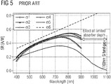
- conventional photodiode structure only provide a comparably small absorber thickness. Due to thin Absorber thickness in integrated photo diodes, however, the spectral responsivity is far below the theoretically possible limit of 0.89A/W at 1100nm (see Figure 5 ).
- FIG. 5 shows example spectral responsivities of integrated silicon PIN photodiode.
- ⁇ 1 relates to an integrated photo diode homogeneous substrate
- ⁇ 2 an integrated photo diode with EPI substrate
- T EPI 20 ⁇ m
- ⁇ 3 an integrated photo diode EPI substrate
- T EPI 40 ⁇ m
- ⁇ 4 an integrated photo diode EPI substrate
- T EPI 60 ⁇ m
- ⁇ 5 a commercial photo diode silicon
- ⁇ 6 indicates the theoretical limit of spectral responsivity.
- the proposed semiconductor device employs an optical coupling layer which comprises an optical coupler and at least a first lateral absorber region.
- the lateral absorber region comprises an absorber material with a bandgap E g in the infrared, IR, e.g. in the near-infrared, NIR.
- IR infrared
- NIR near-infrared
- the absorption bandgap can be extended into the IR, e.g. as for Si-Ge up to approximately 1250 nm.
- the optical coupler allows for deflecting incident light towards the first lateral absorber region. This effectively extends lateral absorption and provides much higher signal-to-noise in the IR compared to conventional vertically stacked photodiode concepts.
- IR infrared
- NIR near infrared
- a semiconductor device for infrared detection comprises a stack of a first semiconductor layer, a second semiconductor layer and an optical coupling layer.
- the first semiconductor layer has a first type of conductivity and the second semiconductor layer has a second type of conductivity.
- the optical coupling layer comprises an optical coupler and at least a first lateral absorber region.
- the optical coupler is configured to deflect incident light towards the first lateral absorber region.
- the first lateral absorber region comprises an absorber material with a bandgap, e.g. in the infrared, IR, or in the near infrared, NIR.
- the semiconductor device is operated as a photodiode, for example.
- Light which is incident of the device traverses through the second semiconductor layer and may strike the optical coupling layer.
- the optical coupler deflects the received light towards the first lateral absorber region.
- the deflected light is guided along the optical coupler and the first lateral absorber region, e.g. along a plane defined by the semiconductor layers. This way the incident light can be coupled into a depletion layer which can be formed between the semiconductor layers.
- Light then traverses along the first lateral absorber region and may be absorbed along the path.
- Absorption process is largely determined by the material properties of the first lateral absorber region. Having a bandgap further (compared to pure Silicon) in the IR or NIR, the absorber material allows for increased absorption in the infrared and especially in the near infrared. Depending on composition of the alloy, absorption can be extended up to some 1800 nm. Furthermore, the optical coupler allows for deflecting incident light towards the lateral absorber regions. This effectively extends lateral absorption cross-section and depth, thus, increasing the absorption volume. This way sensitivity of the semiconductor device can be increased (with respect to bare Silicon) in the IR and/or NIR up to approximately 1250 nm, or more. Ultimately this leads to much higher signal-to-noise in the IR and/or NIR when compared to conventional vertically stacked photodiode concepts.
- the absorber material has a bandgap, e.g. smaller in value than the bandgap for Silicon, e.g. equals 1.1 eV.
- the bandgap for pure or bulk Silicon reduces sensitivity of conventional semiconductor devices in the IR and NIR.
- Absorber materials such as Si-Ge alloy, are available, such as Ge and GeSn, for example. These absorber materials support that the device can be used as a photodiode, e.g. a pn junction or PIN structure can be formed in the layers of the device.
- the absorber materials are compatible with semiconductor technology, such as wafer level processing and Complementary metal-oxide-semiconductor, CMOS, technology, for example.
- the absorber material comprises a strained Silicon Germanium, Si-Ge, alloy.
- Si-Ge alloy has a characteristic bandgap E g ⁇ 0.66 eV which is smaller in value than the bandgap for Silicon.
- the bandgap lies in the near infrared, NIR.
- the Si-Ge alloy constitutes a layer of Silicon in which the Silicon atoms are stretched beyond their normal interatomic distance.
- the characteristic bandgap E g of the Si-Ge alloy can be defined during processing of the lateral absorber region. Basically, the characteristic bandgap E g depends on relative amounts of Silicon and Germanium used to form the alloy.
- the Si-Ge alloy can be monolithically integrated into the semiconductor device by means of epitaxial growing the alloy onto the second semiconductor layer, for example.
- various relative amounts of Silicon and Germanium can be used to form the alloy.
- the compositions of the alloy range between a maximum relative amount of Silicon of 100% and a minimum relative amount of Silicon of 0%.
- the Silicon Germanium alloy ranges between a maximum relative amount of Germanium of 100% and a minimum relative amount of Germanium of 0%. These relative amounts may be considered as limits and the actual compositions may lie in-between these limits.
- a SiGe layer typically has a transition region where the Ge content is practically very low e.g. 0% (and Si concentration is nearly 100%) or vice versa. For pure Ge there may be up to 100% Ge and 0% Si on top of an intermediate region where the Ge content changes from 100% to 0% (and Si concentration changes from 0% to 100%).
- the Silicon Germanium alloy has a relative amount of Silicon of at least 70% and a relative amount of Germanium of at most 30%.
- the actual composition, i.e. relative amounts of Silicon and Germanium may depend on the intended bandgap.
- a Si-Ge alloy with 25% Silicon and 75% Germanium provides a bandgap of 0.66 eV and a penetration depth of ⁇ 50 ⁇ m for NIR. The higher the Ge content the lower the penetration depth becomes.
- the optical coupler comprises a photonic grating integrated into the optical coupling layer.
- the optical coupler comprises an edge coupler.
- the optical coupling layer may be part of a Silicon Germanium-on-insulator, SGOI, or Silicon-On-Insulator, SOI, wafer.
- the optical coupling layer may be layered between the first and second semiconductor layers.
- the optical coupling layer can be implemented using a Silicon Germanium alloy.
- the optical coupling layer may be used as optical waveguide as well.
- the optical coupling layer buried in the SOI or SGOI wafer enables propagation of infrared light in the semiconductor layers on the basis of total internal reflection.
- the photonic grating comprises a plurality of trenches filled with a dielectric.
- the trenches are configured to form a photonic blaze grating.
- the photonic blaze grating allows for coupling incident light into the semiconductor device and direct said light towards the first lateral absorber region.
- the trenches can be configured to solve the grating equation for an intended wavelength of incident light.
- the first type of conductivity is n-type conductivity and the second type of conductivity is p-type conductivity, or vice versa.
- the optical coupling layer comprises a second lateral absorber region which is made of the absorber material. Furthermore, the optical coupler is configured to deflect incident light both towards the first and the second lateral absorber regions. Using two lateral absorber regions further extends absorption volume and sensitivity of the semiconductor device. Corresponding absorption paths can be established, e.g. guiding the incident light towards respective electrodes.
- a first contact region is arranged contiguous with the first lateral absorber region to form a first electrode.
- a second contact region is arranged contiguous with the second lateral absorber region to form a second electrode.
- the electrodes may both be arranged at a front side of the semiconductor device, or, at least one of the electrodes, be arranged at a backside. This allows for front side or backside contacting the semiconductor device.
- the grating is configured to focus deflected incident light onto the first and/or second contact region.
- a backend layer is arranged on the first lateral absorber region, the second lateral absorber region and/or the optical coupling layer.
- the backend layer further comprises a first metallization associated with the first lateral absorber region to form the first electrode.
- a second metallization is associated with the second contact region to form the second electrode. The metallization allows for contacting and/or connecting the electrodes, respectively.
- an infrared detector comprises at least one semiconductor device for infrared detection according to the concept proposed above. Furthermore, a driver circuit is implemented to operate the semiconductor device. In addition, or alternatively, a signal processor is used to process sensor signals to be generated by the semiconductor device.
- the infrared detector comprising the semiconductor device may be a fully integrated device with driver circuit and/or signal processor integrated on the same die.
- a method of manufacturing a semiconductor device for infrared detection comprises the following steps. First, a first semiconductor layer is provided with a first type of conductivity and a second semiconductor layer is provided with a second type of conductivity. An optical coupling layer is provided with an optical coupler and a first lateral absorber region. The first semiconductor layer, the second semiconductor layer and the optical coupling layer are stacked to form the semiconductor device. The optical coupler is configured to deflect incident light towards the first lateral absorber region.
- the first lateral absorber region is made of an absorber material having a bandgap, e.g. in the infrared.
- the method can be executed at wafer level and is compatible to manufacturing technology such as CMOS processing.
- absorption properties can determined by the absorber material properties of the first lateral absorber region. Having a bandgap further (compared to pure Silicon) in the IR or NIR, the absorber material allows for increased absorption in the infrared and especially in the near infrared. Depending on composition of the alloy, absorption can be extended up to some 1800 nm.
- the optical coupler can be manufactured using silicon photonic technology. This effectively extends lateral absorption cross-section and depth, thus, increasing the absorption volume. This way sensitivity of the semiconductor device can be increased (with respect to bare Silicon) in the IR and/or NIR up to approximately 1250 nm, or more. Ultimately this leads to much higher signal-to-noise in the IR and/or NIR when compared to conventional vertically stacked photodiode concepts.
- the first lateral absorber region is formed by means of a strained Silicon Germanium, Si-Ge, alloy.
- the lateral absorber region is monolithically integrated into the optical coupling layer.
- Si-Ge alloy has a characteristic bandgap E g ⁇ 0.66 eV which is smaller in value than the bandgap for Silicon.
- the bandgap lies in the near infrared, NIR.
- the Si-Ge alloy constitutes a layer of Silicon in which the Silicon atoms are stretched beyond their normal interatomic distance.
- the characteristic bandgap E g of the Si-Ge alloy can be defined during processing of the lateral absorber region. Basically, the characteristic bandgap E g depends on relative amounts of Silicon and Germanium used to form the alloy.
- the Si-Ge alloy can be monolithically integrated into the semiconductor device by means of epitaxial growing the alloy onto the second semiconductor layer, for example.
- the Silicon Germanium alloy can be manufactured with various relative amount of Silicon vs. Germanium.
- the compositions of the alloy range between a maximum relative amount of Silicon of 100% and a minimum relative amount of Silicon of 0%.
- the Silicon Germanium alloy ranges between a maximum relative amount of Germanium of 100% and a minimum relative amount of Germanium of 0%. These relative amounts may be considered as limits and the actual compositions may lie in-between these limits.
- the Silicon Germanium alloy has a relative amount of Silicon of at least 70% and a relative amount of Germanium of at most 30%.
- the actual composition, i.e. relative amounts of Silicon and Germanium may depend on the intended bandgap. For example, a SI-Ge alloy with 25% Silicon and 75% Germanium provides a bandgap of 0.66 eV and a penetration depth of ⁇ 50 ⁇ m for NIR.
- the optical coupler is configured as a photonic grating and integrating in the optical coupling layer. This involves forming a plurality of trenches filled with an oxide, wherein the trenches are arranged to form a photonic blaze grating.
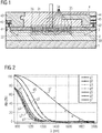
- Figure 1 shows an example embodiment of a semiconductor device for infrared detection.
- the device comprises a stack of a first semiconductor layer 1, a second semiconductor layer 2 and an optical coupling layer 3. Furthermore, a backend layer 4 is arranged on top of the stack 1, 2, 3.
- the first semiconductor layer 1 has a first type of conductivity, such as n-type or p-type.
- the first semiconductor layer 1 is of p-type conductivity.
- the first semiconductor layer is made from p-type CMOS bulk Silicon.
- the conductivity may be reversed and the first semiconductor layer has n-type conductivity.
- the second semiconductor layer 2 is arranged on a main surface of the first semiconductor layer 1.
- the second semiconductor layer 2 has a second type of conductivity, such as n-type or p-type.
- the second semiconductor layer 2 is of n-type conductivity.
- the second semiconductor layer is made from n-type CMOS bulk Silicon.
- the conductivity may be reversed and the second semiconductor layer has p-type conductivity.
- the first and second semiconductor layers are arranged as pn-junction such that a depletion region or space charge region is formed between the layers.
- the optical coupling layer 3 is arranged on a main surface 21 of the second semiconductor layer 2. For example, at least in parts, the optical coupling layer 3 is contiguous with the depletion region formed between the first and second semiconductor layers.
- the optical coupling layer 3 comprises an optical coupler 31 and two lateral absorber regions 32, 33.
- the optical coupler 31 is designed as a grating coupler, or surface coupler, for vertical coupling (vertical with respect to the main surface 21 of the second semiconductor layer, for example). In other embodiments (not shown) the optical coupler can be implemented by edge couplers, inverted taper or adiabatic couplers, for instance.
- the grating coupler further comprises trenches 33, which are filled with a dielectric material, e.g. an oxide.
- the trenches are arranged to form a photonic grating (see Figures 4A to 4C ).
- the photonic grating forms a photonic Blaze grating.
- the individual trenches constitute lines of the grating and are spaced apart with a line spacing according to the grating equation. For example, considering a wavelength of 1300 nm (NIR) the trenches are spaced apart by some 325 nm.
- NIR 1300 nm
- the lateral absorber regions 32, 33 flank the optical coupler 31.
- the optical coupler 31 has two output sides 35 which are coupled to and facing the lateral absorber regions 32, 33, respectively.
- the lateral absorber regions 32, 33 are made of an absorber material with a characteristic bandgap E g in the infrared, IR.
- the bandgap lies in the near infrared, NIR.
- the lateral absorber regions made from the Si-Ge alloy constitute layers of Silicon in which the Silicon atoms are stretched beyond their normal interatomic distance.
- the strain present in the layer constrains the feasible layer thickness, which lies at some 150 nm, for example. Larger layer thickness, however, may relax the Si-Ge alloy.
- the characteristic bandgap E g of the Si-Ge alloy can be defined during processing of the lateral absorber regions. Basically, the characteristic bandgap E g depends on relative amounts of Silicon and Germanium used to form the alloy. Further details will be discussed with respect to Figure 2 .
- the Si-Ge alloy can be monolithically integrated into the semiconductor device by means of epitaxial growing the alloy onto the second semiconductor layer, for example.
- the semiconductor device comprises the backend layer 4, e.g. a CMOS backend layer, which is arranged on the second semiconductor layer 2, i.e. the backend layer 4 covers a main surface of the second semiconductor layer 2.
- a first contact region 41 and a second contact region 42 are arranged in the backend layer 4.
- the first contact region 41 is contiguous with the first lateral absorber region 32 and forms a first electrode 43.
- the second contact region 42 is contiguous with the second lateral absorber region 33 and forms a second electrode 44.
- the electrodes 43, 44 are connected to a metallization layer 45 in the backend layer 4 which allows for electrically contacting the semiconductor device.
- the backend layer 4 may include further contacts, insulating layers (dielectrics), metal levels, and bonding sites for chip-to-package connections etc.
- the backend layer 4 is made from a material which is at least partly transparent in the IR or NIR.
- the semiconductor device is operated as a photodiode, for example.
- Light which is incident of the device traverses through the backend layer 4 and eventually strikes the optical coupling layer 3.
- the optical coupler receives the incident light and deflects the received light, by means of diffraction by the photonic grating, deflects towards the lateral absorber regions 32, 33.
- light is guided into a plane defined by the semiconductor layers, e.g. parallel to said plane. This way the incident light is coupled into the depletion layer formed by the semiconductor layers.
- Light then traverses along the lateral absorber regions 32, 33 and eventually gets absorbed along the path.
- Absorption process is largely determined by the material properties of the lateral absorber regions 32, 33.
- the optical coupler i.e.
- photonic grating in this embodiment allows for deflecting incident light towards the lateral absorber regions. This effectively extends lateral absorption cross-section and depth, thus, increasing the absorption volume.
- Si-Ge alloy as material for the lateral absorption regions increases sensitivity (with respect to bare Silicon) in the IR and/or NIR up to approximately 1250 nm, or more. Ultimately this leads to much higher signal-to-noise in the IR and/or NIR when compared to conventional vertically stacked photodiode concepts.
- the first and second semiconductor layers may be arranged in different ways.
- the two semiconductor layers may be embedded in an epilayer.
- the two layers may be stacked in a vertical fashion as discussed above, or horizontally, side-by-side.
- the semiconductor layers may form a PIN junction with an intrinsic region in-between the layers and the depletion region exists almost completely within the intrinsic region. This way the semiconductor device can be operated as a PIN photodiode.
- contacting may also be implemented from a backside of the first semiconductor layer, e.g. by means of solder balls and a redistribution layer.
- Figure 2 shows examples of Silicon-Germanium composition.
- the drawing depicts absorbance Abs (in units of %) as a function of wavelength ⁇ (in units of nm).
- Six graphs are shown which represent different relative amounts of Silicon and Germanium, respectively.
- Graphs g1 and g7 show pure Silicon and pure Germanium as a reference, respectively.
- graph g1 indicates the bandgap E g of Silicon as absorbance approximately reaches zero for ⁇ > 1100 nm.
- Pure Germanium however, has non-zero absorbance at 1100 nm up to approximately 1850 nm.
- the following table gives an overview of the relative amounts represented by the graphs g1 to g7.
- the graphs show that with increasing relative amount of Germanium, Ge, the bandgap of the Si-Ge alloy is shifted further into the IR. Absorbance has been measured in 10 ⁇ m bulk of Si(1-x)Ge(x) and Ge, wherein x represents the relative amount of Si and Ge. A relative amount of Si of 70% to 80% and a corresponding relative amount of Ge of 30% to 40% has been found suitable for a number of NIR applications.
- Figure 3 shows penetration depths of examples of Silicon-Germanium alloy compositions.
- the drawing depicts penetration depth (in units of ⁇ m) for various wavelength ⁇ (in units of nm) of incident light as a function of alloy composition Si(1-x)Ge(x).
- ⁇ 1 800 nm
- ⁇ 2 900 nm
- ⁇ 3 1000 nm
- ⁇ 4 1100 nm.
- the dashed line in the drawing indicates the alloy composition of graph g6 with 25% relative amount of Si and 75% relative amount of Ge. It is apparent that Si-Ge alloys with higher relative amounts of Ge provide increasing penetration depth for NIR light, effectively increasing the absorption volume of the lateral absorber regions.
- FIGS 4A to 4C show examples of the optical coupling layer.
- the optical coupler is arranged as photonic grating having a plurality of trenches 33 which are filled with a dielectric, e.g. an oxide.
- the drawing shows the trenches 33 in top view.
- the trenches are configured to form a photonic blaze grating which obeys the grating equation.
- the trenches are arranged in a plane with a constant line spacing.
- the trenches forming the grating are coupled to a tapered region 36, such as an adiabatic taper, which forms part of an output side 35 of the photonic blaze grating.
- the lateral absorption regions are coupled to a respective output side 35 of the photonic blaze grating in order to receive light from the grating.
- the incident light (indicated by the arrows in the drawings) is deflected towards to the output side 35 by means of diffraction.
- the transverse mode of the incident is guided towards the output side 35.
- the optical coupler may be integrated into the semiconductor layers, there by forming a fully integrated semiconductor device for infrared detection. In other embodiments the optical coupler may be attached to the semiconductor layers.
- Figure 4A shows an optical coupler with one output side.
- Figure 4B shows an optical coupler with a dual tilted design and two output sides, respectively.
- Figure 4C shows an optical coupler with curved trenches. Curvature of the trenches is configured to focus deflected incident light, e.g. onto the first and/or second contact regions.
Landscapes
- Physics & Mathematics (AREA)
- General Physics & Mathematics (AREA)
- Optics & Photonics (AREA)
- Engineering & Computer Science (AREA)
- Microelectronics & Electronic Packaging (AREA)
- Power Engineering (AREA)
- Light Receiving Elements (AREA)
- Solid State Image Pick-Up Elements (AREA)
- Photometry And Measurement Of Optical Pulse Characteristics (AREA)
Abstract
Description
- The invention relates to the field of infrared photodetectors. Improved concepts are introduced that relate to a semiconductor device for infrared detection, a method of manufacturing semiconductor device for infrared detection and an infrared detector.
- Conventional photodiodes, such as pn- or pin-photodiodes are based on a vertical layer stack (with respect to a wafer surface) of p-type, n-type, and/or intrinsic semiconductor layers to form anode, cathode and light absorber regions. Semiconductor materials, such as Silicon have an energy gap or bandgap, i.e. an energy range in a solid where no electron states can exist. For Silicon the bandgap is about Eg = 1.1 eV. The bandgap generally refers to the energy difference (in electron volts) between the top of the valence band and the bottom of the conduction band in insulators and semiconductors. In other words, the bandgap indicates the energy required to promote a valence electron bound to an atom to become a conduction electron, which is free to move within the crystal lattice and serve as a charge carrier to conduct electric current. Photodiodes made from Silicon have a responsivity which is low or even equals zero for wavelengths higher than 1100 nm due to the bandgap at Eg = 1.1 eV. Furthermore, conventional photodiode structure only provide a comparably small absorber thickness. Due to thin Absorber thickness in integrated photo diodes, however, the spectral responsivity is far below the theoretically possible limit of 0.89A/W at 1100nm (see
Figure 5 ). InFigure 5 shows example spectral responsivities of integrated silicon PIN photodiode. For example, σ1 relates to an integrated photo diode homogeneous substrate, σ2 an integrated photo diode with EPI substrate (TEPI = 20 µm), σ3 an integrated photo diode EPI substrate (TEPI = 40 µm), σ4 an integrated photo diode EPI substrate (TEPI = 60 µm), σ5 a commercial photo diode silicon, and σ6 indicates the theoretical limit of spectral responsivity. - It is an objective to provide a semiconductor device for infrared detection, a method of manufacturing a semiconductor device for infrared detection and an infrared detector which allow for increased sensitivity in the near infrared.
- These objectives are achieved by the subject matter of the independent claims. Further developments and embodiments are described in dependent claims.
- It is to be understood that any feature described in relation to any one embodiment may be used alone, or in combination with other features described herein, and may also be used in combination with one or more features of any other of the embodiments, or any combination of any other of the embodiments unless described as an alternative. Furthermore, equivalents and modifications not described below may also be employed without departing from the scope of the semiconductor device, the method of manufacturing a semiconductor device for infrared detection and the infrared detector which are defined in the accompanying claims.
- The following relates to an improved concept in the field of semiconductor optoelectronic devices, e.g. photodiodes. The proposed semiconductor device employs an optical coupling layer which comprises an optical coupler and at least a first lateral absorber region. The lateral absorber region comprises an absorber material with a bandgap Eg in the infrared, IR, e.g. in the near-infrared, NIR. For example, strained Silicon-Germanium alloy as absorber material has a bandgap Eg smaller in value than the bandgap for Silicon of Eg = 1.1 eV. The absorption bandgap can be extended into the IR, e.g. as for Si-Ge up to approximately 1250 nm. Furthermore, the optical coupler allows for deflecting incident light towards the first lateral absorber region. This effectively extends lateral absorption and provides much higher signal-to-noise in the IR compared to conventional vertically stacked photodiode concepts.
- In the following, the term "infrared", or IR, refers to electromagnetic radiation having a wavelength in the range of 700 nm to 1 mm. "Near infrared", or NIR, refers to electromagnetic radiation having a wavelength in the range of 0.70 to 1.4 µm.
- In at least one embodiment a semiconductor device for infrared detection comprises a stack of a first semiconductor layer, a second semiconductor layer and an optical coupling layer. The first semiconductor layer has a first type of conductivity and the second semiconductor layer has a second type of conductivity. The optical coupling layer comprises an optical coupler and at least a first lateral absorber region. The optical coupler is configured to deflect incident light towards the first lateral absorber region. The first lateral absorber region comprises an absorber material with a bandgap, e.g. in the infrared, IR, or in the near infrared, NIR.
- The semiconductor device is operated as a photodiode, for example. Light which is incident of the device traverses through the second semiconductor layer and may strike the optical coupling layer. The optical coupler deflects the received light towards the first lateral absorber region. The deflected light is guided along the optical coupler and the first lateral absorber region, e.g. along a plane defined by the semiconductor layers. This way the incident light can be coupled into a depletion layer which can be formed between the semiconductor layers. Light then traverses along the first lateral absorber region and may be absorbed along the path.
- Absorption process is largely determined by the material properties of the first lateral absorber region. Having a bandgap further (compared to pure Silicon) in the IR or NIR, the absorber material allows for increased absorption in the infrared and especially in the near infrared. Depending on composition of the alloy, absorption can be extended up to some 1800 nm. Furthermore, the optical coupler allows for deflecting incident light towards the lateral absorber regions. This effectively extends lateral absorption cross-section and depth, thus, increasing the absorption volume. This way sensitivity of the semiconductor device can be increased (with respect to bare Silicon) in the IR and/or NIR up to approximately 1250 nm, or more. Ultimately this leads to much higher signal-to-noise in the IR and/or NIR when compared to conventional vertically stacked photodiode concepts.
- In at least one embodiment the absorber material has a bandgap, e.g. smaller in value than the bandgap for Silicon, e.g. equals 1.1 eV. The bandgap for pure or bulk Silicon reduces sensitivity of conventional semiconductor devices in the IR and NIR. Absorber materials, such as Si-Ge alloy, are available, such as Ge and GeSn, for example. These absorber materials support that the device can be used as a photodiode, e.g. a pn junction or PIN structure can be formed in the layers of the device. Furthermore, the absorber materials are compatible with semiconductor technology, such as wafer level processing and Complementary metal-oxide-semiconductor, CMOS, technology, for example.
- In at least one embodiment the absorber material comprises a strained Silicon Germanium, Si-Ge, alloy. Si-Ge alloy has a characteristic bandgap Eg∼0.66 eV which is smaller in value than the bandgap for Silicon. The bandgap lies in the near infrared, NIR. The Si-Ge alloy constitutes a layer of Silicon in which the Silicon atoms are stretched beyond their normal interatomic distance. The characteristic bandgap Eg of the Si-Ge alloy can be defined during processing of the lateral absorber region. Basically, the characteristic bandgap Eg depends on relative amounts of Silicon and Germanium used to form the alloy. The Si-Ge alloy can be monolithically integrated into the semiconductor device by means of epitaxial growing the alloy onto the second semiconductor layer, for example.
- In embodiments of the semiconductor device various relative amounts of Silicon and Germanium can be used to form the alloy. The compositions of the alloy range between a maximum relative amount of Silicon of 100% and a minimum relative amount of Silicon of 0%. Furthermore, the Silicon Germanium alloy ranges between a maximum relative amount of Germanium of 100% and a minimum relative amount of Germanium of 0%. These relative amounts may be considered as limits and the actual compositions may lie in-between these limits. A SiGe layer typically has a transition region where the Ge content is practically very low e.g. 0% (and Si concentration is nearly 100%) or vice versa. For pure Ge there may be up to 100% Ge and 0% Si on top of an intermediate region where the Ge content changes from 100% to 0% (and Si concentration changes from 0% to 100%).
- Alternatively, the Silicon Germanium alloy has a relative amount of Silicon of at least 70% and a relative amount of Germanium of at most 30%. The actual composition, i.e. relative amounts of Silicon and Germanium may depend on the intended bandgap. For example, a Si-Ge alloy with 25% Silicon and 75% Germanium provides a bandgap of 0.66 eV and a penetration depth of <50 µm for NIR. The higher the Ge content the lower the penetration depth becomes.
- In at least one embodiment the optical coupler comprises a photonic grating integrated into the optical coupling layer. In addition, or alternatively, the optical coupler comprises an edge coupler.
- In at least one embodiment the optical coupling layer may be part of a Silicon Germanium-on-insulator, SGOI, or Silicon-On-Insulator, SOI, wafer. The optical coupling layer may be layered between the first and second semiconductor layers. For example, the optical coupling layer can be implemented using a Silicon Germanium alloy. Furthermore, the optical coupling layer may be used as optical waveguide as well. For example, the optical coupling layer buried in the SOI or SGOI wafer enables propagation of infrared light in the semiconductor layers on the basis of total internal reflection.
- In at least one embodiment the photonic grating comprises a plurality of trenches filled with a dielectric. The trenches are configured to form a photonic blaze grating. The photonic blaze grating allows for coupling incident light into the semiconductor device and direct said light towards the first lateral absorber region. The trenches can be configured to solve the grating equation for an intended wavelength of incident light.
- In at least one embodiment the first type of conductivity is n-type conductivity and the second type of conductivity is p-type conductivity, or vice versa.
- In at least one embodiment the optical coupling layer comprises a second lateral absorber region which is made of the absorber material. Furthermore, the optical coupler is configured to deflect incident light both towards the first and the second lateral absorber regions. Using two lateral absorber regions further extends absorption volume and sensitivity of the semiconductor device. Corresponding absorption paths can be established, e.g. guiding the incident light towards respective electrodes.
- In at least one embodiment a first contact region is arranged contiguous with the first lateral absorber region to form a first electrode. In addition, or alternatively, a second contact region is arranged contiguous with the second lateral absorber region to form a second electrode. The electrodes may both be arranged at a front side of the semiconductor device, or, at least one of the electrodes, be arranged at a backside. This allows for front side or backside contacting the semiconductor device.
- In at least one embodiment the grating is configured to focus deflected incident light onto the first and/or second contact region.
- In at least one embodiment a backend layer is arranged on the first lateral absorber region, the second lateral absorber region and/or the optical coupling layer. The backend layer further comprises a first metallization associated with the first lateral absorber region to form the first electrode. In addition, or alternatively, a second metallization is associated with the second contact region to form the second electrode. The metallization allows for contacting and/or connecting the electrodes, respectively.
- In at least one embodiment an infrared detector comprises at least one semiconductor device for infrared detection according to the concept proposed above. Furthermore, a driver circuit is implemented to operate the semiconductor device. In addition, or alternatively, a signal processor is used to process sensor signals to be generated by the semiconductor device. The infrared detector comprising the semiconductor device may be a fully integrated device with driver circuit and/or signal processor integrated on the same die.
- In at least one embodiment a method of manufacturing a semiconductor device for infrared detection comprises the following steps. First, a first semiconductor layer is provided with a first type of conductivity and a second semiconductor layer is provided with a second type of conductivity. An optical coupling layer is provided with an optical coupler and a first lateral absorber region. The first semiconductor layer, the second semiconductor layer and the optical coupling layer are stacked to form the semiconductor device. The optical coupler is configured to deflect incident light towards the first lateral absorber region. The first lateral absorber region is made of an absorber material having a bandgap, e.g. in the infrared.
- The method can be executed at wafer level and is compatible to manufacturing technology such as CMOS processing. For example, absorption properties can determined by the absorber material properties of the first lateral absorber region. Having a bandgap further (compared to pure Silicon) in the IR or NIR, the absorber material allows for increased absorption in the infrared and especially in the near infrared. Depending on composition of the alloy, absorption can be extended up to some 1800 nm. Furthermore, the optical coupler can be manufactured using silicon photonic technology. This effectively extends lateral absorption cross-section and depth, thus, increasing the absorption volume. This way sensitivity of the semiconductor device can be increased (with respect to bare Silicon) in the IR and/or NIR up to approximately 1250 nm, or more. Ultimately this leads to much higher signal-to-noise in the IR and/or NIR when compared to conventional vertically stacked photodiode concepts.
- In at least one embodiment the first lateral absorber region is formed by means of a strained Silicon Germanium, Si-Ge, alloy. The lateral absorber region is monolithically integrated into the optical coupling layer. Si-Ge alloy has a characteristic bandgap Eg∼0.66 eV which is smaller in value than the bandgap for Silicon. The bandgap lies in the near infrared, NIR. The Si-Ge alloy constitutes a layer of Silicon in which the Silicon atoms are stretched beyond their normal interatomic distance. The characteristic bandgap Eg of the Si-Ge alloy can be defined during processing of the lateral absorber region. Basically, the characteristic bandgap Eg depends on relative amounts of Silicon and Germanium used to form the alloy. The Si-Ge alloy can be monolithically integrated into the semiconductor device by means of epitaxial growing the alloy onto the second semiconductor layer, for example.
- The Silicon Germanium alloy can be manufactured with various relative amount of Silicon vs. Germanium. The compositions of the alloy range between a maximum relative amount of Silicon of 100% and a minimum relative amount of Silicon of 0%. Furthermore, the Silicon Germanium alloy ranges between a maximum relative amount of Germanium of 100% and a minimum relative amount of Germanium of 0%. These relative amounts may be considered as limits and the actual compositions may lie in-between these limits. Alternatively, the Silicon Germanium alloy has a relative amount of Silicon of at least 70% and a relative amount of Germanium of at most 30%. The actual composition, i.e. relative amounts of Silicon and Germanium may depend on the intended bandgap. For example, a SI-Ge alloy with 25% Silicon and 75% Germanium provides a bandgap of 0.66 eV and a penetration depth of <50 µm for NIR.
- In at least one embodiment the optical coupler is configured as a photonic grating and integrating in the optical coupling layer. This involves forming a plurality of trenches filled with an oxide, wherein the trenches are arranged to form a photonic blaze grating.
- Further implementations of the method of manufacturing semiconductor device for infrared detection are readily derived from the various implementations and embodiments of the semiconductor device for infrared detection and infrared detector, and vice versa.
- In the following, the concept presented above is described in further detail with respect to drawings, in which examples of embodiments are presented. In the embodiments and Figures presented hereinafter, similar or identical elements may each be provided with the same reference numerals. The elements illustrated in the drawings and their size relationships among one another, however, should not be regarded as true to scale, rather individual elements, such as layers, components, and regions, may be exaggerated to enable better illustration or a better understanding.
- Figure 1
- shows an example embodiment of semiconductor device for infrared detection,
- Figure 2
- shows examples of Silicon-Germanium alloy composition,
- Figure 3
- shows penetration depths of examples of Silicon-Germanium alloy compositions,
- Figures 4A to 4C
- show examples of an optical coupling layer, and
- Figure 5
- shows examples of prior art silicon photodiodes with silicon epilayer of different thickness.
-
Figure 1 shows an example embodiment of a semiconductor device for infrared detection. The device comprises a stack of a first semiconductor layer 1, asecond semiconductor layer 2 and anoptical coupling layer 3. Furthermore, a backend layer 4 is arranged on top of thestack - The first semiconductor layer 1 has a first type of conductivity, such as n-type or p-type. In this embodiment the first semiconductor layer 1 is of p-type conductivity. For example, the first semiconductor layer is made from p-type CMOS bulk Silicon. In other embodiments (not shown) the conductivity may be reversed and the first semiconductor layer has n-type conductivity. The
second semiconductor layer 2 is arranged on a main surface of the first semiconductor layer 1. Thesecond semiconductor layer 2 has a second type of conductivity, such as n-type or p-type. In this embodiment thesecond semiconductor layer 2 is of n-type conductivity. For example, the second semiconductor layer is made from n-type CMOS bulk Silicon. In other embodiments (not shown) the conductivity may be reversed and the second semiconductor layer has p-type conductivity. For example, the first and second semiconductor layers are arranged as pn-junction such that a depletion region or space charge region is formed between the layers. - The
optical coupling layer 3 is arranged on amain surface 21 of thesecond semiconductor layer 2. For example, at least in parts, theoptical coupling layer 3 is contiguous with the depletion region formed between the first and second semiconductor layers. Theoptical coupling layer 3 comprises anoptical coupler 31 and twolateral absorber regions optical coupler 31 is designed as a grating coupler, or surface coupler, for vertical coupling (vertical with respect to themain surface 21 of the second semiconductor layer, for example). In other embodiments (not shown) the optical coupler can be implemented by edge couplers, inverted taper or adiabatic couplers, for instance. The grating coupler further comprisestrenches 33, which are filled with a dielectric material, e.g. an oxide. The trenches are arranged to form a photonic grating (seeFigures 4A to 4C ). In this embodiment the photonic grating forms a photonic Blaze grating. The individual trenches constitute lines of the grating and are spaced apart with a line spacing according to the grating equation. For example, considering a wavelength of 1300 nm (NIR) the trenches are spaced apart by some 325 nm. - Two
lateral absorber regions optical coupler 31. Theoptical coupler 31 has twooutput sides 35 which are coupled to and facing thelateral absorber regions lateral absorber regions Figure 2 . The Si-Ge alloy can be monolithically integrated into the semiconductor device by means of epitaxial growing the alloy onto the second semiconductor layer, for example. - Furthermore, the semiconductor device comprises the backend layer 4, e.g. a CMOS backend layer, which is arranged on the
second semiconductor layer 2, i.e. the backend layer 4 covers a main surface of thesecond semiconductor layer 2. Afirst contact region 41 and asecond contact region 42 are arranged in the backend layer 4. In fact, thefirst contact region 41 is contiguous with the firstlateral absorber region 32 and forms afirst electrode 43. Thesecond contact region 42 is contiguous with the secondlateral absorber region 33 and forms asecond electrode 44. Theelectrodes metallization layer 45 in the backend layer 4 which allows for electrically contacting the semiconductor device. The backend layer 4 may include further contacts, insulating layers (dielectrics), metal levels, and bonding sites for chip-to-package connections etc. The backend layer 4 is made from a material which is at least partly transparent in the IR or NIR. - The semiconductor device is operated as a photodiode, for example. Light which is incident of the device traverses through the backend layer 4 and eventually strikes the
optical coupling layer 3. The optical coupler receives the incident light and deflects the received light, by means of diffraction by the photonic grating, deflects towards thelateral absorber regions lateral absorber regions - Absorption process is largely determined by the material properties of the
lateral absorber regions - In other embodiments (not shown) the first and second semiconductor layers may be arranged in different ways. For example, the two semiconductor layers may be embedded in an epilayer. Furthermore, the two layers may be stacked in a vertical fashion as discussed above, or horizontally, side-by-side. Instead of forming a pn-junction the semiconductor layers may form a PIN junction with an intrinsic region in-between the layers and the depletion region exists almost completely within the intrinsic region. This way the semiconductor device can be operated as a PIN photodiode. Instead of contacting the semiconductor device from the front-side, which is exposed to incident light, contacting may also be implemented from a backside of the first semiconductor layer, e.g. by means of solder balls and a redistribution layer.
-
Figure 2 shows examples of Silicon-Germanium composition. The drawing depicts absorbance Abs (in units of %) as a function of wavelength λ (in units of nm). Six graphs are shown which represent different relative amounts of Silicon and Germanium, respectively. Graphs g1 and g7 show pure Silicon and pure Germanium as a reference, respectively. For example, graph g1 indicates the bandgap Eg of Silicon as absorbance approximately reaches zero for λ > 1100 nm. Pure Germanium, however, has non-zero absorbance at 1100 nm up to approximately 1850 nm. The following table gives an overview of the relative amounts represented by the graphs g1 to g7.graph Si [in %] Ge [in %] g1 100 0 g2 90 10 g3 80 20 g4 70 30 g5 50 50 g6 25 75 g7 0 100 - The graphs show that with increasing relative amount of Germanium, Ge, the bandgap of the Si-Ge alloy is shifted further into the IR. Absorbance has been measured in 10 µm bulk of Si(1-x)Ge(x) and Ge, wherein x represents the relative amount of Si and Ge. A relative amount of Si of 70% to 80% and a corresponding relative amount of Ge of 30% to 40% has been found suitable for a number of NIR applications.
-
Figure 3 shows penetration depths of examples of Silicon-Germanium alloy compositions. The drawing depicts penetration depth (in units of µm) for various wavelength λ (in units of nm) of incident light as a function of alloy composition Si(1-x)Ge(x). Four wavelengths are depicted: λ1 = 800 nm, λ2 = 900 nm, λ3 = 1000 nm, and λ4 = 1100 nm. The dashed line in the drawing indicates the alloy composition of graph g6 with 25% relative amount of Si and 75% relative amount of Ge. It is apparent that Si-Ge alloys with higher relative amounts of Ge provide increasing penetration depth for NIR light, effectively increasing the absorption volume of the lateral absorber regions. -
Figures 4A to 4C show examples of the optical coupling layer. The optical coupler is arranged as photonic grating having a plurality oftrenches 33 which are filled with a dielectric, e.g. an oxide. The drawing shows thetrenches 33 in top view. The trenches are configured to form a photonic blaze grating which obeys the grating equation. For example, the trenches are arranged in a plane with a constant line spacing. The trenches forming the grating are coupled to a taperedregion 36, such as an adiabatic taper, which forms part of anoutput side 35 of the photonic blaze grating. The lateral absorption regions (not shown) are coupled to arespective output side 35 of the photonic blaze grating in order to receive light from the grating. The incident light (indicated by the arrows in the drawings) is deflected towards to theoutput side 35 by means of diffraction. Typically, the transverse mode of the incident is guided towards theoutput side 35. The optical coupler may be integrated into the semiconductor layers, there by forming a fully integrated semiconductor device for infrared detection. In other embodiments the optical coupler may be attached to the semiconductor layers.Figure 4A shows an optical coupler with one output side.Figure 4B shows an optical coupler with a dual tilted design and two output sides, respectively.Figure 4C shows an optical coupler with curved trenches. Curvature of the trenches is configured to focus deflected incident light, e.g. onto the first and/or second contact regions. -
- 1
- first semiconductor layer
- 2
- second semiconductor layer
- 3
- optical coupling layer
- 4
- backend layer
- 31
- optical coupler
- 32
- lateral absorber region
- 33
- lateral absorber region
- 34
- trench
- 35
- output side of optical coupler
- 41
- contact area
- 42
- contact area
- 43
- electrode
- 44
- electrode
- 45
- metallization
- g1 to g7
- graphs
- λ1 to λ4
- wavelengths of incident light
- λ
- wavelength
Claims (15)
- A semiconductor device for infrared detection, comprising a stack of a first semiconductor layer (1), a second semiconductor layer (2) and an optical coupling layer (3), wherein:- the first semiconductor layer (1) has a first type of conductivity and the second semiconductor layer (2) has a second type of conductivity,- the optical coupling layer (3) comprises an optical coupler (31) and at least a first lateral absorber region (32),- the optical coupler (31) is configured to deflect incident light towards the first lateral absorber region (32), and- the first lateral absorber region (32) comprises an absorber material with a bandgap Eg in the infrared, IR.
- The semiconductor device according to claim 1, wherein the absorber material has a bandgap Eg smaller in value than the bandgap for Silicon of Eg = 1.1 eV.
- The semiconductor device according to claim 1 or 2, wherein the absorber material comprises a strained Silicon Germanium, Si-Ge, alloy.
- The semiconductor device according to claim 3, wherein the Si-Ge alloy- has a maximum relative amount of Si of 100% and a minimum relative amount of Si of 0%, and- has a maximum relative amount of Ge of 100% and a minimum relative amount of Ge of 0%, or the Si-Ge alloy- has a relative amount of Si of at least 70% and a relative amount of Ge of at most 30%.
- The semiconductor device according to one of claims 1 to 4, wherein- the optical coupler (31) comprises a photonic grating integrated into the optical coupling layer (3), and/or- the optical coupling layer (3) is part of a Silicon Germanium-on-insulator, SGOI, or Silicon-On-Insulator, SOI, wafer.
- The semiconductor device according to claim 5, wherein- the photonic grating comprises a plurality of trenches filled with a dielectric, and- the trenches are configured to form a photonic Blaze grating.
- The semiconductor device according to one of claims 1 to 6, wherein the first type of conductivity is n-type conductivity and the second type of conductivity is p-type conductivity, or vice versa.
- The semiconductor device according to one of claims 1 to 7, wherein- the optical coupling layer (3) comprises a second lateral absorber region (33) made of the absorber material, and- the optical coupler (31) is configured to deflect incident light both towards the first and the second lateral absorber region (32, 33).
- The semiconductor device according to claim 8, wherein- a first contact region (4) is arranged contiguous with the first lateral absorber region (32) to form a first electrode, and/or- a second contact region (5) is arranged contiguous with the second lateral absorber region (33) to form a second electrode and/or wherein- the grating is configured to focus deflected incident light onto the first and/or second contact region (4, 5) .
- The semiconductor device according to claim 9, wherein- a backend layer (6) is arranged on the first lateral absorber region (32), the second lateral absorber region (33) and/or the optical coupling layer (3), and the backend layer (6) further comprises:- a first metallization associated with the first lateral absorber region (32) to form the first electrode, and/or- a second metallization associated with the second contact region (5) to form the second electrode.
- An infrared detector, comprising:- at least one semiconductor device for infrared detection according to one of claims 1 to 10, and- a driver circuit to operate the semiconductor device, and/or- a signal processor to process sensor signals to be generated by the semiconductor device.
- A method of manufacturing semiconductor device for infrared detection, comprising the steps of:- providing a first semiconductor layer (1) with a first type of conductivity and a second semiconductor layer (2) with a second type of conductivity,- providing an optical coupling layer (3) with an optical coupler (31) and a first lateral absorber region (32),- stacking the first semiconductor layer (1), second semiconductor layer (2) and optical coupling layer (3) to form the semiconductor device; wherein:- the optical coupler (31) is configured to deflect incident light towards the first lateral absorber region (32), and- the first lateral absorber region (32) is made of an absorber material with a bandgap Eg in the infrared, IR.
- The method according to claim 12, wherein the first lateral absorber region (32) is formed by means of a strained Silicon Germanium, Si-Ge, alloy, and monolithically integrated into the optical coupling layer (3).
- The method according to claim 13, wherein the Si-Ge alloy- has a maximum relative amount of Si of 100% and a minimum relative amount of Si of 0%, and- has a maximum relative amount of Ge of 100% and a minimum relative amount of Si of 0%, or the Si-Ge alloy- has a relative amount of Si of at least 70% and a relative amount of Ge of at least 30%.
- The method according to claim 12 or 13, wherein the optical coupler (31) is configured as a photonic grating and integrated in the optical coupling layer (3) involving forming plurality of trenches filled with an oxide, the trenches are arranged to form a photonic Blaze grating.
Priority Applications (4)
| Application Number | Priority Date | Filing Date | Title |
|---|---|---|---|
| EP19180949.0A EP3754730B1 (en) | 2019-06-18 | 2019-06-18 | Semiconductor device for infrared detection, method of manufacturing semiconductor device for infrared detection and infrared detector |
| CN202080044693.8A CN114026702B (en) | 2019-06-18 | 2020-06-04 | Semiconductor device for infrared detection, method for manufacturing semiconductor device for infrared detection, and infrared detector |
| US17/620,059 US11923467B2 (en) | 2019-06-18 | 2020-06-04 | Semiconductor device for infrared detection, method of manufacturing semiconductor device for infrared detection and infrared detector |
| PCT/EP2020/065454 WO2020254119A1 (en) | 2019-06-18 | 2020-06-04 | Semiconductor device for infrared detection, method of manufacturing semiconductor device for infrared detection and infrared detector |
Applications Claiming Priority (1)
| Application Number | Priority Date | Filing Date | Title |
|---|---|---|---|
| EP19180949.0A EP3754730B1 (en) | 2019-06-18 | 2019-06-18 | Semiconductor device for infrared detection, method of manufacturing semiconductor device for infrared detection and infrared detector |
Publications (2)
| Publication Number | Publication Date |
|---|---|
| EP3754730A1 true EP3754730A1 (en) | 2020-12-23 |
| EP3754730B1 EP3754730B1 (en) | 2023-01-18 |
Family
ID=66998185
Family Applications (1)
| Application Number | Title | Priority Date | Filing Date |
|---|---|---|---|
| EP19180949.0A Active EP3754730B1 (en) | 2019-06-18 | 2019-06-18 | Semiconductor device for infrared detection, method of manufacturing semiconductor device for infrared detection and infrared detector |
Country Status (4)
| Country | Link |
|---|---|
| US (1) | US11923467B2 (en) |
| EP (1) | EP3754730B1 (en) |
| CN (1) | CN114026702B (en) |
| WO (1) | WO2020254119A1 (en) |
Citations (6)
| Publication number | Priority date | Publication date | Assignee | Title |
|---|---|---|---|---|
| JPS61242070A (en) * | 1985-04-19 | 1986-10-28 | Matsushita Electric Ind Co Ltd | Semiconductor optical element |
| US20050053347A1 (en) * | 2003-05-29 | 2005-03-10 | Applied Materials, Inc. | Impurity-based waveguide detectors |
| US20110038588A1 (en) * | 2009-08-14 | 2011-02-17 | Electronics And Telecommunications Research Institute | Optical coupler |
| US20160161331A1 (en) * | 2014-12-03 | 2016-06-09 | Technische Universitat Berlin | Optical sensor |
| CN106328751A (en) * | 2015-07-02 | 2017-01-11 | 中兴通讯股份有限公司 | Silicon-based germanium photodetector |
| CN109461787A (en) * | 2018-09-29 | 2019-03-12 | 北京工业大学 | The vertical coupled type of grating, which is inserted, refers to photodetector |
Family Cites Families (12)
| Publication number | Priority date | Publication date | Assignee | Title |
|---|---|---|---|---|
| JPH0720329A (en) * | 1993-06-23 | 1995-01-24 | Canon Inc | Optical multiplexer / demultiplexer |
| DE19515369B4 (en) * | 1995-05-02 | 2007-05-24 | Colour Control Farbmeßtechnik GmbH | Spectrally selective photodiode with diffractive structures |
| JP3717104B2 (en) * | 2000-05-30 | 2005-11-16 | シャープ株式会社 | Photo detector with built-in circuit |
| KR100706743B1 (en) | 2005-05-20 | 2007-04-11 | (주)실리콘화일 | Silicon-Germanium Photodiodes for Image Sensors |
| JP5232981B2 (en) * | 2008-03-07 | 2013-07-10 | 日本電気株式会社 | SiGe photodiode |
| GB2507512A (en) | 2012-10-31 | 2014-05-07 | Ibm | Semiconductor device with epitaxially grown active layer adjacent a subsequently grown optically passive region |
| US9287432B2 (en) | 2013-07-23 | 2016-03-15 | SiFotonics Technologies Co, Ltd. | Ge—Si P-I-N photodiode with reduced dark current and fabrication method thereof |
| US9413140B2 (en) * | 2013-12-19 | 2016-08-09 | Taiwan Semiconductor Manufacturing Company Limited | Semiconductor arrangement and formation thereof |
| AU2015274800A1 (en) | 2014-06-09 | 2017-01-05 | Stc.Unm | Integrated bound-mode spectral/angular sensors |
| US10408934B2 (en) * | 2015-08-19 | 2019-09-10 | Canon Kabushiki Kaisha | Object information acquiring apparatus |
| CN113727000A (en) * | 2016-05-27 | 2021-11-30 | 松下知识产权经营株式会社 | Image pickup system |
| CN109817730B (en) * | 2018-12-29 | 2024-08-20 | 华进半导体封装先导技术研发中心有限公司 | Photodetector and manufacturing method thereof |
-
2019
- 2019-06-18 EP EP19180949.0A patent/EP3754730B1/en active Active
-
2020
- 2020-06-04 CN CN202080044693.8A patent/CN114026702B/en active Active
- 2020-06-04 US US17/620,059 patent/US11923467B2/en active Active
- 2020-06-04 WO PCT/EP2020/065454 patent/WO2020254119A1/en not_active Ceased
Patent Citations (6)
| Publication number | Priority date | Publication date | Assignee | Title |
|---|---|---|---|---|
| JPS61242070A (en) * | 1985-04-19 | 1986-10-28 | Matsushita Electric Ind Co Ltd | Semiconductor optical element |
| US20050053347A1 (en) * | 2003-05-29 | 2005-03-10 | Applied Materials, Inc. | Impurity-based waveguide detectors |
| US20110038588A1 (en) * | 2009-08-14 | 2011-02-17 | Electronics And Telecommunications Research Institute | Optical coupler |
| US20160161331A1 (en) * | 2014-12-03 | 2016-06-09 | Technische Universitat Berlin | Optical sensor |
| CN106328751A (en) * | 2015-07-02 | 2017-01-11 | 中兴通讯股份有限公司 | Silicon-based germanium photodetector |
| CN109461787A (en) * | 2018-09-29 | 2019-03-12 | 北京工业大学 | The vertical coupled type of grating, which is inserted, refers to photodetector |
Also Published As
| Publication number | Publication date |
|---|---|
| WO2020254119A1 (en) | 2020-12-24 |
| CN114026702A (en) | 2022-02-08 |
| US11923467B2 (en) | 2024-03-05 |
| CN114026702B (en) | 2024-07-05 |
| EP3754730B1 (en) | 2023-01-18 |
| US20220310857A1 (en) | 2022-09-29 |
Similar Documents
| Publication | Publication Date | Title |
|---|---|---|
| US12113078B2 (en) | Photodetector | |
| CN110870070B (en) | High-speed optical sensing equipment II | |
| US11749696B2 (en) | High-speed light sensing apparatus II | |
| CN108140656B (en) | Wide-frequency spectrum optical sensor | |
| CN110800110B (en) | Resonator enhanced image sensor | |
| TW201904034A (en) | Germanium-silicon light sensing apparatus | |
| US20230197758A1 (en) | Photodetecting device with enhanced collection efficiency | |
| EP3586365A1 (en) | Short-wave infrared detector array and method for the manufacturing thereof | |
| US20230187462A1 (en) | Semiconductor light detection element | |
| EP4083656B1 (en) | Light detector, light detection system, lidar device, and mobile body | |
| KR20140030265A (en) | Passivated upstanding nanostructures and methods of making the same | |
| JP7109718B2 (en) | Compound semiconductor photodiode array | |
| EP3754730B1 (en) | Semiconductor device for infrared detection, method of manufacturing semiconductor device for infrared detection and infrared detector | |
| JP7798958B2 (en) | Light receiving element and method for assembling the same |
Legal Events
| Date | Code | Title | Description |
|---|---|---|---|
| PUAI | Public reference made under article 153(3) epc to a published international application that has entered the european phase |
Free format text: ORIGINAL CODE: 0009012 |
|
| STAA | Information on the status of an ep patent application or granted ep patent |
Free format text: STATUS: THE APPLICATION HAS BEEN PUBLISHED |
|
| AK | Designated contracting states |
Kind code of ref document: A1 Designated state(s): AL AT BE BG CH CY CZ DE DK EE ES FI FR GB GR HR HU IE IS IT LI LT LU LV MC MK MT NL NO PL PT RO RS SE SI SK SM TR |
|
| AX | Request for extension of the european patent |
Extension state: BA ME |
|
| STAA | Information on the status of an ep patent application or granted ep patent |
Free format text: STATUS: REQUEST FOR EXAMINATION WAS MADE |
|
| 17P | Request for examination filed |
Effective date: 20210622 |
|
| RBV | Designated contracting states (corrected) |
Designated state(s): AL AT BE BG CH CY CZ DE DK EE ES FI FR GB GR HR HU IE IS IT LI LT LU LV MC MK MT NL NO PL PT RO RS SE SI SK SM TR |
|
| GRAP | Despatch of communication of intention to grant a patent |
Free format text: ORIGINAL CODE: EPIDOSNIGR1 |
|
| STAA | Information on the status of an ep patent application or granted ep patent |
Free format text: STATUS: GRANT OF PATENT IS INTENDED |
|
| GRAS | Grant fee paid |
Free format text: ORIGINAL CODE: EPIDOSNIGR3 |
|
| INTG | Intention to grant announced |
Effective date: 20221109 |
|
| GRAA | (expected) grant |
Free format text: ORIGINAL CODE: 0009210 |
|
| STAA | Information on the status of an ep patent application or granted ep patent |
Free format text: STATUS: THE PATENT HAS BEEN GRANTED |
|
| AK | Designated contracting states |
Kind code of ref document: B1 Designated state(s): AL AT BE BG CH CY CZ DE DK EE ES FI FR GB GR HR HU IE IS IT LI LT LU LV MC MK MT NL NO PL PT RO RS SE SI SK SM TR |
|
| REG | Reference to a national code |
Ref country code: GB Ref legal event code: FG4D |
|
| REG | Reference to a national code |
Ref country code: CH Ref legal event code: EP |
|
| REG | Reference to a national code |
Ref country code: DE Ref legal event code: R096 Ref document number: 602019024477 Country of ref document: DE |
|
| REG | Reference to a national code |
Ref country code: AT Ref legal event code: REF Ref document number: 1545163 Country of ref document: AT Kind code of ref document: T Effective date: 20230215 Ref country code: IE Ref legal event code: FG4D |
|
| REG | Reference to a national code |
Ref country code: LT Ref legal event code: MG9D |
|
| REG | Reference to a national code |
Ref country code: NL Ref legal event code: MP Effective date: 20230118 |
|
| REG | Reference to a national code |
Ref country code: AT Ref legal event code: MK05 Ref document number: 1545163 Country of ref document: AT Kind code of ref document: T Effective date: 20230118 |
|
| PG25 | Lapsed in a contracting state [announced via postgrant information from national office to epo] |
Ref country code: NL Free format text: LAPSE BECAUSE OF FAILURE TO SUBMIT A TRANSLATION OF THE DESCRIPTION OR TO PAY THE FEE WITHIN THE PRESCRIBED TIME-LIMIT Effective date: 20230118 |
|
| PG25 | Lapsed in a contracting state [announced via postgrant information from national office to epo] |
Ref country code: RS Free format text: LAPSE BECAUSE OF FAILURE TO SUBMIT A TRANSLATION OF THE DESCRIPTION OR TO PAY THE FEE WITHIN THE PRESCRIBED TIME-LIMIT Effective date: 20230118 Ref country code: PT Free format text: LAPSE BECAUSE OF FAILURE TO SUBMIT A TRANSLATION OF THE DESCRIPTION OR TO PAY THE FEE WITHIN THE PRESCRIBED TIME-LIMIT Effective date: 20230518 Ref country code: NO Free format text: LAPSE BECAUSE OF FAILURE TO SUBMIT A TRANSLATION OF THE DESCRIPTION OR TO PAY THE FEE WITHIN THE PRESCRIBED TIME-LIMIT Effective date: 20230418 Ref country code: LV Free format text: LAPSE BECAUSE OF FAILURE TO SUBMIT A TRANSLATION OF THE DESCRIPTION OR TO PAY THE FEE WITHIN THE PRESCRIBED TIME-LIMIT Effective date: 20230118 Ref country code: LT Free format text: LAPSE BECAUSE OF FAILURE TO SUBMIT A TRANSLATION OF THE DESCRIPTION OR TO PAY THE FEE WITHIN THE PRESCRIBED TIME-LIMIT Effective date: 20230118 Ref country code: HR Free format text: LAPSE BECAUSE OF FAILURE TO SUBMIT A TRANSLATION OF THE DESCRIPTION OR TO PAY THE FEE WITHIN THE PRESCRIBED TIME-LIMIT Effective date: 20230118 Ref country code: ES Free format text: LAPSE BECAUSE OF FAILURE TO SUBMIT A TRANSLATION OF THE DESCRIPTION OR TO PAY THE FEE WITHIN THE PRESCRIBED TIME-LIMIT Effective date: 20230118 Ref country code: AT Free format text: LAPSE BECAUSE OF FAILURE TO SUBMIT A TRANSLATION OF THE DESCRIPTION OR TO PAY THE FEE WITHIN THE PRESCRIBED TIME-LIMIT Effective date: 20230118 |
|
| PG25 | Lapsed in a contracting state [announced via postgrant information from national office to epo] |
Ref country code: SE Free format text: LAPSE BECAUSE OF FAILURE TO SUBMIT A TRANSLATION OF THE DESCRIPTION OR TO PAY THE FEE WITHIN THE PRESCRIBED TIME-LIMIT Effective date: 20230118 Ref country code: PL Free format text: LAPSE BECAUSE OF FAILURE TO SUBMIT A TRANSLATION OF THE DESCRIPTION OR TO PAY THE FEE WITHIN THE PRESCRIBED TIME-LIMIT Effective date: 20230118 Ref country code: IS Free format text: LAPSE BECAUSE OF FAILURE TO SUBMIT A TRANSLATION OF THE DESCRIPTION OR TO PAY THE FEE WITHIN THE PRESCRIBED TIME-LIMIT Effective date: 20230518 Ref country code: GR Free format text: LAPSE BECAUSE OF FAILURE TO SUBMIT A TRANSLATION OF THE DESCRIPTION OR TO PAY THE FEE WITHIN THE PRESCRIBED TIME-LIMIT Effective date: 20230419 Ref country code: FI Free format text: LAPSE BECAUSE OF FAILURE TO SUBMIT A TRANSLATION OF THE DESCRIPTION OR TO PAY THE FEE WITHIN THE PRESCRIBED TIME-LIMIT Effective date: 20230118 |
|
| P01 | Opt-out of the competence of the unified patent court (upc) registered |
Effective date: 20230822 |
|
| REG | Reference to a national code |
Ref country code: DE Ref legal event code: R097 Ref document number: 602019024477 Country of ref document: DE |
|
| PG25 | Lapsed in a contracting state [announced via postgrant information from national office to epo] |
Ref country code: SM Free format text: LAPSE BECAUSE OF FAILURE TO SUBMIT A TRANSLATION OF THE DESCRIPTION OR TO PAY THE FEE WITHIN THE PRESCRIBED TIME-LIMIT Effective date: 20230118 Ref country code: RO Free format text: LAPSE BECAUSE OF FAILURE TO SUBMIT A TRANSLATION OF THE DESCRIPTION OR TO PAY THE FEE WITHIN THE PRESCRIBED TIME-LIMIT Effective date: 20230118 Ref country code: EE Free format text: LAPSE BECAUSE OF FAILURE TO SUBMIT A TRANSLATION OF THE DESCRIPTION OR TO PAY THE FEE WITHIN THE PRESCRIBED TIME-LIMIT Effective date: 20230118 Ref country code: DK Free format text: LAPSE BECAUSE OF FAILURE TO SUBMIT A TRANSLATION OF THE DESCRIPTION OR TO PAY THE FEE WITHIN THE PRESCRIBED TIME-LIMIT Effective date: 20230118 Ref country code: CZ Free format text: LAPSE BECAUSE OF FAILURE TO SUBMIT A TRANSLATION OF THE DESCRIPTION OR TO PAY THE FEE WITHIN THE PRESCRIBED TIME-LIMIT Effective date: 20230118 |
|
| PLBE | No opposition filed within time limit |
Free format text: ORIGINAL CODE: 0009261 |
|
| STAA | Information on the status of an ep patent application or granted ep patent |
Free format text: STATUS: NO OPPOSITION FILED WITHIN TIME LIMIT |
|
| PG25 | Lapsed in a contracting state [announced via postgrant information from national office to epo] |
Ref country code: SK Free format text: LAPSE BECAUSE OF FAILURE TO SUBMIT A TRANSLATION OF THE DESCRIPTION OR TO PAY THE FEE WITHIN THE PRESCRIBED TIME-LIMIT Effective date: 20230118 |
|
| 26N | No opposition filed |
Effective date: 20231019 |
|
| PG25 | Lapsed in a contracting state [announced via postgrant information from national office to epo] |
Ref country code: MC Free format text: LAPSE BECAUSE OF FAILURE TO SUBMIT A TRANSLATION OF THE DESCRIPTION OR TO PAY THE FEE WITHIN THE PRESCRIBED TIME-LIMIT Effective date: 20230118 |
|
| PG25 | Lapsed in a contracting state [announced via postgrant information from national office to epo] |
Ref country code: SI Free format text: LAPSE BECAUSE OF FAILURE TO SUBMIT A TRANSLATION OF THE DESCRIPTION OR TO PAY THE FEE WITHIN THE PRESCRIBED TIME-LIMIT Effective date: 20230118 Ref country code: MC Free format text: LAPSE BECAUSE OF FAILURE TO SUBMIT A TRANSLATION OF THE DESCRIPTION OR TO PAY THE FEE WITHIN THE PRESCRIBED TIME-LIMIT Effective date: 20230118 |
|
| REG | Reference to a national code |
Ref country code: CH Ref legal event code: PL |
|
| REG | Reference to a national code |
Ref country code: BE Ref legal event code: MM Effective date: 20230630 |
|
| GBPC | Gb: european patent ceased through non-payment of renewal fee |
Effective date: 20230618 |
|
| PG25 | Lapsed in a contracting state [announced via postgrant information from national office to epo] |
Ref country code: LU Free format text: LAPSE BECAUSE OF NON-PAYMENT OF DUE FEES Effective date: 20230618 |
|
| REG | Reference to a national code |
Ref country code: IE Ref legal event code: MM4A |
|
| PG25 | Lapsed in a contracting state [announced via postgrant information from national office to epo] |
Ref country code: LU Free format text: LAPSE BECAUSE OF NON-PAYMENT OF DUE FEES Effective date: 20230618 |
|
| PG25 | Lapsed in a contracting state [announced via postgrant information from national office to epo] |
Ref country code: IE Free format text: LAPSE BECAUSE OF NON-PAYMENT OF DUE FEES Effective date: 20230618 |
|
| PG25 | Lapsed in a contracting state [announced via postgrant information from national office to epo] |
Ref country code: IE Free format text: LAPSE BECAUSE OF NON-PAYMENT OF DUE FEES Effective date: 20230618 Ref country code: GB Free format text: LAPSE BECAUSE OF NON-PAYMENT OF DUE FEES Effective date: 20230618 Ref country code: CH Free format text: LAPSE BECAUSE OF NON-PAYMENT OF DUE FEES Effective date: 20230630 |
|
| PG25 | Lapsed in a contracting state [announced via postgrant information from national office to epo] |
Ref country code: IT Free format text: LAPSE BECAUSE OF FAILURE TO SUBMIT A TRANSLATION OF THE DESCRIPTION OR TO PAY THE FEE WITHIN THE PRESCRIBED TIME-LIMIT Effective date: 20230118 Ref country code: FR Free format text: LAPSE BECAUSE OF NON-PAYMENT OF DUE FEES Effective date: 20230630 Ref country code: BE Free format text: LAPSE BECAUSE OF NON-PAYMENT OF DUE FEES Effective date: 20230630 |
|
| PGFP | Annual fee paid to national office [announced via postgrant information from national office to epo] |
Ref country code: DE Payment date: 20240619 Year of fee payment: 6 |
|
| PG25 | Lapsed in a contracting state [announced via postgrant information from national office to epo] |
Ref country code: BG Free format text: LAPSE BECAUSE OF FAILURE TO SUBMIT A TRANSLATION OF THE DESCRIPTION OR TO PAY THE FEE WITHIN THE PRESCRIBED TIME-LIMIT Effective date: 20230118 |
|
| REG | Reference to a national code |
Ref country code: DE Ref legal event code: R079 Ref document number: 602019024477 Country of ref document: DE Free format text: PREVIOUS MAIN CLASS: H01L0031109000 Ipc: H10F0030222000 |
|
| PG25 | Lapsed in a contracting state [announced via postgrant information from national office to epo] |
Ref country code: BG Free format text: LAPSE BECAUSE OF FAILURE TO SUBMIT A TRANSLATION OF THE DESCRIPTION OR TO PAY THE FEE WITHIN THE PRESCRIBED TIME-LIMIT Effective date: 20230118 |
|
| PG25 | Lapsed in a contracting state [announced via postgrant information from national office to epo] |
Ref country code: CY Free format text: LAPSE BECAUSE OF FAILURE TO SUBMIT A TRANSLATION OF THE DESCRIPTION OR TO PAY THE FEE WITHIN THE PRESCRIBED TIME-LIMIT; INVALID AB INITIO Effective date: 20190618 |
|
| PG25 | Lapsed in a contracting state [announced via postgrant information from national office to epo] |
Ref country code: HU Free format text: LAPSE BECAUSE OF FAILURE TO SUBMIT A TRANSLATION OF THE DESCRIPTION OR TO PAY THE FEE WITHIN THE PRESCRIBED TIME-LIMIT; INVALID AB INITIO Effective date: 20190618 |
|
| PG25 | Lapsed in a contracting state [announced via postgrant information from national office to epo] |
Ref country code: TR Free format text: LAPSE BECAUSE OF FAILURE TO SUBMIT A TRANSLATION OF THE DESCRIPTION OR TO PAY THE FEE WITHIN THE PRESCRIBED TIME-LIMIT Effective date: 20230118 |
|
| REG | Reference to a national code |
Ref country code: DE Ref legal event code: R119 Ref document number: 602019024477 Country of ref document: DE |
|
| PG25 | Lapsed in a contracting state [announced via postgrant information from national office to epo] |
Ref country code: DE Free format text: LAPSE BECAUSE OF NON-PAYMENT OF DUE FEES Effective date: 20260101 |