EP3752888B1 - Data storage using light of spatially modulated phase and polarization - Google Patents
Data storage using light of spatially modulated phase and polarization Download PDFInfo
- Publication number
- EP3752888B1 EP3752888B1 EP18837002.7A EP18837002A EP3752888B1 EP 3752888 B1 EP3752888 B1 EP 3752888B1 EP 18837002 A EP18837002 A EP 18837002A EP 3752888 B1 EP3752888 B1 EP 3752888B1
- Authority
- EP
- European Patent Office
- Prior art keywords
- polarization
- substrate
- data
- light
- phase
- Prior art date
- Legal status (The legal status is an assumption and is not a legal conclusion. Google has not performed a legal analysis and makes no representation as to the accuracy of the status listed.)
- Active
Links
Images



Classifications
-
- G—PHYSICS
- G11—INFORMATION STORAGE
- G11B—INFORMATION STORAGE BASED ON RELATIVE MOVEMENT BETWEEN RECORD CARRIER AND TRANSDUCER
- G11B7/00—Recording or reproducing by optical means, e.g. recording using a thermal beam of optical radiation by modifying optical properties or the physical structure, reproducing using an optical beam at lower power by sensing optical properties; Record carriers therefor
- G11B7/12—Heads, e.g. forming of the optical beam spot or modulation of the optical beam
- G11B7/125—Optical beam sources therefor, e.g. laser control circuitry specially adapted for optical storage devices; Modulators, e.g. means for controlling the size or intensity of optical spots or optical traces
- G11B7/127—Lasers; Multiple laser arrays
-
- G—PHYSICS
- G02—OPTICS
- G02B—OPTICAL ELEMENTS, SYSTEMS OR APPARATUS
- G02B27/00—Optical systems or apparatus not provided for by any of the groups G02B1/00 - G02B26/00, G02B30/00
- G02B27/10—Beam splitting or combining systems
- G02B27/1006—Beam splitting or combining systems for splitting or combining different wavelengths
- G02B27/102—Beam splitting or combining systems for splitting or combining different wavelengths for generating a colour image from monochromatic image signal sources
- G02B27/1046—Beam splitting or combining systems for splitting or combining different wavelengths for generating a colour image from monochromatic image signal sources for use with transmissive spatial light modulators
-
- G—PHYSICS
- G03—PHOTOGRAPHY; CINEMATOGRAPHY; ANALOGOUS TECHNIQUES USING WAVES OTHER THAN OPTICAL WAVES; ELECTROGRAPHY; HOLOGRAPHY
- G03H—HOLOGRAPHIC PROCESSES OR APPARATUS
- G03H1/00—Holographic processes or apparatus using light, infrared or ultraviolet waves for obtaining holograms or for obtaining an image from them; Details peculiar thereto
- G03H1/04—Processes or apparatus for producing holograms
- G03H1/0402—Recording geometries or arrangements
- G03H1/041—Optical element in the object space affecting the object beam, not otherwise provided for
-
- G—PHYSICS
- G03—PHOTOGRAPHY; CINEMATOGRAPHY; ANALOGOUS TECHNIQUES USING WAVES OTHER THAN OPTICAL WAVES; ELECTROGRAPHY; HOLOGRAPHY
- G03H—HOLOGRAPHIC PROCESSES OR APPARATUS
- G03H1/00—Holographic processes or apparatus using light, infrared or ultraviolet waves for obtaining holograms or for obtaining an image from them; Details peculiar thereto
- G03H1/04—Processes or apparatus for producing holograms
- G03H1/16—Processes or apparatus for producing holograms using Fourier transform
-
- G—PHYSICS
- G03—PHOTOGRAPHY; CINEMATOGRAPHY; ANALOGOUS TECHNIQUES USING WAVES OTHER THAN OPTICAL WAVES; ELECTROGRAPHY; HOLOGRAPHY
- G03H—HOLOGRAPHIC PROCESSES OR APPARATUS
- G03H1/00—Holographic processes or apparatus using light, infrared or ultraviolet waves for obtaining holograms or for obtaining an image from them; Details peculiar thereto
- G03H1/22—Processes or apparatus for obtaining an optical image from holograms
- G03H1/2294—Addressing the hologram to an active spatial light modulator
-
- G—PHYSICS
- G03—PHOTOGRAPHY; CINEMATOGRAPHY; ANALOGOUS TECHNIQUES USING WAVES OTHER THAN OPTICAL WAVES; ELECTROGRAPHY; HOLOGRAPHY
- G03H—HOLOGRAPHIC PROCESSES OR APPARATUS
- G03H1/00—Holographic processes or apparatus using light, infrared or ultraviolet waves for obtaining holograms or for obtaining an image from them; Details peculiar thereto
- G03H1/26—Processes or apparatus specially adapted to produce multiple sub- holograms or to obtain images from them, e.g. multicolour technique
-
- G—PHYSICS
- G11—INFORMATION STORAGE
- G11B—INFORMATION STORAGE BASED ON RELATIVE MOVEMENT BETWEEN RECORD CARRIER AND TRANSDUCER
- G11B11/00—Recording on or reproducing from the same record carrier wherein for these two operations the methods are covered by different main groups of groups G11B3/00 - G11B7/00 or by different subgroups of group G11B9/00; Record carriers therefor
- G11B11/10—Recording on or reproducing from the same record carrier wherein for these two operations the methods are covered by different main groups of groups G11B3/00 - G11B7/00 or by different subgroups of group G11B9/00; Record carriers therefor using recording by magnetic means or other means for magnetisation or demagnetisation of a record carrier, e.g. light induced spin magnetisation; Demagnetisation by thermal or stress means in the presence or not of an orienting magnetic field
- G11B11/105—Recording on or reproducing from the same record carrier wherein for these two operations the methods are covered by different main groups of groups G11B3/00 - G11B7/00 or by different subgroups of group G11B9/00; Record carriers therefor using recording by magnetic means or other means for magnetisation or demagnetisation of a record carrier, e.g. light induced spin magnetisation; Demagnetisation by thermal or stress means in the presence or not of an orienting magnetic field using a beam of light or a magnetic field for recording by change of magnetisation and a beam of light for reproducing, i.e. magneto-optical, e.g. light-induced thermomagnetic recording, spin magnetisation recording, Kerr or Faraday effect reproducing
- G11B11/10532—Heads
-
- G—PHYSICS
- G11—INFORMATION STORAGE
- G11B—INFORMATION STORAGE BASED ON RELATIVE MOVEMENT BETWEEN RECORD CARRIER AND TRANSDUCER
- G11B7/00—Recording or reproducing by optical means, e.g. recording using a thermal beam of optical radiation by modifying optical properties or the physical structure, reproducing using an optical beam at lower power by sensing optical properties; Record carriers therefor
- G11B7/004—Recording, reproducing or erasing methods; Read, write or erase circuits therefor
- G11B7/0045—Recording
-
- G—PHYSICS
- G11—INFORMATION STORAGE
- G11B—INFORMATION STORAGE BASED ON RELATIVE MOVEMENT BETWEEN RECORD CARRIER AND TRANSDUCER
- G11B7/00—Recording or reproducing by optical means, e.g. recording using a thermal beam of optical radiation by modifying optical properties or the physical structure, reproducing using an optical beam at lower power by sensing optical properties; Record carriers therefor
- G11B7/004—Recording, reproducing or erasing methods; Read, write or erase circuits therefor
- G11B7/0065—Recording, reproducing or erasing by using optical interference patterns, e.g. holograms
-
- G—PHYSICS
- G11—INFORMATION STORAGE
- G11B—INFORMATION STORAGE BASED ON RELATIVE MOVEMENT BETWEEN RECORD CARRIER AND TRANSDUCER
- G11B7/00—Recording or reproducing by optical means, e.g. recording using a thermal beam of optical radiation by modifying optical properties or the physical structure, reproducing using an optical beam at lower power by sensing optical properties; Record carriers therefor
- G11B7/12—Heads, e.g. forming of the optical beam spot or modulation of the optical beam
- G11B7/125—Optical beam sources therefor, e.g. laser control circuitry specially adapted for optical storage devices; Modulators, e.g. means for controlling the size or intensity of optical spots or optical traces
- G11B7/128—Modulators
-
- G—PHYSICS
- G11—INFORMATION STORAGE
- G11B—INFORMATION STORAGE BASED ON RELATIVE MOVEMENT BETWEEN RECORD CARRIER AND TRANSDUCER
- G11B7/00—Recording or reproducing by optical means, e.g. recording using a thermal beam of optical radiation by modifying optical properties or the physical structure, reproducing using an optical beam at lower power by sensing optical properties; Record carriers therefor
- G11B7/12—Heads, e.g. forming of the optical beam spot or modulation of the optical beam
- G11B7/135—Means for guiding the beam from the source to the record carrier or from the record carrier to the detector
- G11B7/1372—Lenses
-
- G—PHYSICS
- G11—INFORMATION STORAGE
- G11B—INFORMATION STORAGE BASED ON RELATIVE MOVEMENT BETWEEN RECORD CARRIER AND TRANSDUCER
- G11B7/00—Recording or reproducing by optical means, e.g. recording using a thermal beam of optical radiation by modifying optical properties or the physical structure, reproducing using an optical beam at lower power by sensing optical properties; Record carriers therefor
- G11B7/12—Heads, e.g. forming of the optical beam spot or modulation of the optical beam
- G11B7/135—Means for guiding the beam from the source to the record carrier or from the record carrier to the detector
- G11B7/1395—Beam splitters or combiners
-
- G—PHYSICS
- G11—INFORMATION STORAGE
- G11B—INFORMATION STORAGE BASED ON RELATIVE MOVEMENT BETWEEN RECORD CARRIER AND TRANSDUCER
- G11B7/00—Recording or reproducing by optical means, e.g. recording using a thermal beam of optical radiation by modifying optical properties or the physical structure, reproducing using an optical beam at lower power by sensing optical properties; Record carriers therefor
- G11B7/12—Heads, e.g. forming of the optical beam spot or modulation of the optical beam
- G11B7/14—Heads, e.g. forming of the optical beam spot or modulation of the optical beam specially adapted to record on, or to reproduce from, more than one track simultaneously
-
- G—PHYSICS
- G03—PHOTOGRAPHY; CINEMATOGRAPHY; ANALOGOUS TECHNIQUES USING WAVES OTHER THAN OPTICAL WAVES; ELECTROGRAPHY; HOLOGRAPHY
- G03H—HOLOGRAPHIC PROCESSES OR APPARATUS
- G03H1/00—Holographic processes or apparatus using light, infrared or ultraviolet waves for obtaining holograms or for obtaining an image from them; Details peculiar thereto
- G03H1/04—Processes or apparatus for producing holograms
- G03H1/0476—Holographic printer
- G03H2001/048—Parallel printer, i.e. a fringe pattern is reproduced
-
- G—PHYSICS
- G03—PHOTOGRAPHY; CINEMATOGRAPHY; ANALOGOUS TECHNIQUES USING WAVES OTHER THAN OPTICAL WAVES; ELECTROGRAPHY; HOLOGRAPHY
- G03H—HOLOGRAPHIC PROCESSES OR APPARATUS
- G03H1/00—Holographic processes or apparatus using light, infrared or ultraviolet waves for obtaining holograms or for obtaining an image from them; Details peculiar thereto
- G03H1/04—Processes or apparatus for producing holograms
- G03H1/0476—Holographic printer
- G03H2001/0482—Interference based printer
-
- G—PHYSICS
- G03—PHOTOGRAPHY; CINEMATOGRAPHY; ANALOGOUS TECHNIQUES USING WAVES OTHER THAN OPTICAL WAVES; ELECTROGRAPHY; HOLOGRAPHY
- G03H—HOLOGRAPHIC PROCESSES OR APPARATUS
- G03H1/00—Holographic processes or apparatus using light, infrared or ultraviolet waves for obtaining holograms or for obtaining an image from them; Details peculiar thereto
- G03H1/04—Processes or apparatus for producing holograms
- G03H1/0476—Holographic printer
- G03H2001/0484—Arranged to produce three-dimensional fringe pattern
-
- G—PHYSICS
- G03—PHOTOGRAPHY; CINEMATOGRAPHY; ANALOGOUS TECHNIQUES USING WAVES OTHER THAN OPTICAL WAVES; ELECTROGRAPHY; HOLOGRAPHY
- G03H—HOLOGRAPHIC PROCESSES OR APPARATUS
- G03H1/00—Holographic processes or apparatus using light, infrared or ultraviolet waves for obtaining holograms or for obtaining an image from them; Details peculiar thereto
- G03H1/26—Processes or apparatus specially adapted to produce multiple sub- holograms or to obtain images from them, e.g. multicolour technique
- G03H2001/2605—Arrangement of the sub-holograms, e.g. partial overlapping
-
- G—PHYSICS
- G03—PHOTOGRAPHY; CINEMATOGRAPHY; ANALOGOUS TECHNIQUES USING WAVES OTHER THAN OPTICAL WAVES; ELECTROGRAPHY; HOLOGRAPHY
- G03H—HOLOGRAPHIC PROCESSES OR APPARATUS
- G03H2210/00—Object characteristics
- G03H2210/30—3D object
-
- G—PHYSICS
- G03—PHOTOGRAPHY; CINEMATOGRAPHY; ANALOGOUS TECHNIQUES USING WAVES OTHER THAN OPTICAL WAVES; ELECTROGRAPHY; HOLOGRAPHY
- G03H—HOLOGRAPHIC PROCESSES OR APPARATUS
- G03H2223/00—Optical components
- G03H2223/22—Polariser
-
- G—PHYSICS
- G03—PHOTOGRAPHY; CINEMATOGRAPHY; ANALOGOUS TECHNIQUES USING WAVES OTHER THAN OPTICAL WAVES; ELECTROGRAPHY; HOLOGRAPHY
- G03H—HOLOGRAPHIC PROCESSES OR APPARATUS
- G03H2225/00—Active addressable light modulator
- G03H2225/30—Modulation
- G03H2225/36—Polarisation
-
- G—PHYSICS
- G03—PHOTOGRAPHY; CINEMATOGRAPHY; ANALOGOUS TECHNIQUES USING WAVES OTHER THAN OPTICAL WAVES; ELECTROGRAPHY; HOLOGRAPHY
- G03H—HOLOGRAPHIC PROCESSES OR APPARATUS
- G03H2225/00—Active addressable light modulator
- G03H2225/60—Multiple SLMs
Definitions
- High-power, short-pulse laser irradiance can be used to write and store data within a glass substrate.
- the irradiance induces a long-lived lattice perturbation at its focus, which derives from non-linear, two-photon absorption by the substrate.
- the lattice perturbation has the optical properties of a nano-grating embedded within the substrate at the point where the irradiance is imaged.
- Data written to a glass substrate in this manner can be read back using a polarized optical beam to interrogate the various grating-like perturbations formed within it.
- JP 2014 211935 A describes an optical information recording apparatus capable of recording or reproducing information with a simpler configuration using holographic recording or polarization holographic recording.
- An irradiation light generation system generates signal light having a polarization component in which information is recorded by spatial modulation of at least one of phase and amplitude as + 1st order diffracted light or -1st order diffracted light, while generating reference light as described above
- the + 1st order diffracted light and 0th order light corresponding to the -1st order diffracted light are generated.
- the irradiation system 4 records the information on the recording medium 2 as a three-dimensional optical anisotropy distribution by irradiating the recording medium 2 having photosensitivity with the signal light and the reference light.
- the phase-modulated recorded signal is converted into an intensity-modulated beam that can be easily detected using a conventional image sensor.
- SRH can be used effectively for holographic data storage and phase-to-intensity conversion.
- US 2001/002895 A1 describes that an optical storage medium of the present invention enables storage of data with high precision at high speed, and rewriting of data at high speed without an erasing process.
- Optical storage, reading and retrieving methods and optical storage, reading, and retrieving apparatuses using the medium are also provided.
- the optical storage medium has at least a polarization-sensitive member having the photo-induced birefringence property, such as a member made of polyester polymer having cyanoazobenzene as a side chain.
- the above apparatuses have spatial light modulator capable of modulating polarization.
- the modulator provides information of bit of two-dimensional data to each corresponding pixel by application or non-application of a voltage, and modulates the polarization of the beam incident on each pixel.
- a signal beam transmitted through the spatial light modulator having a spatial polarization modulation corresponding to the two-dimensional data is obtained.
- the signal beam illuminates the optical storage medium, and at the same time, a reference beam illuminates the same region in the medium where the signal beam illuminates.
- a hologram of the polarization modulation of the signal beam corresponding to the two-dimensional data is stored in the optical storage medium.
- a hologram record apparatus includes a spatial light modulator and a control device.
- the spatial light modulator is arranged on an optical path of signal light (L1) and divided into a plurality of cell blocks arranged in a matrix. Each of the cell blocks is further divided into a plurality of cells arranged in a matrix.
- the spatial light modulator can perform modulation on the cell basis.
- the control device controls the spatial light modulator so as to modulate the signal light according to a plurality of record information sets to be recorded on a hologram record medium. Pluralities of modulation units existing in the same cell block are not made into identical patterns.
- All the multiple information bits that are stored within all the photochromic chemicals in each addressable domain are read in common, and induced to simultaneously fluoresce, again by process of 2-P absorption.
- the fluorescence of each of different photochromic chemical in each addressed domain-which fluorescence is selective in accordance with the written state of each such photochromic chemical- is separated from, and is separately detected from, the fluorescence of all other photochromic chemicals because it is of a unique color, and is spatially steered to an associated detector array, normally a Charge Coupled Device (CCD), by a monochromator, normally a prism.
- Exemplary fluorescent photochromic chemicals are spirobenzopyran, rhodamine, cumarin and anthracene.
- Suitable groups of photochromic chemicals are formed from individual photochromic chemicals exhibiting narrow, sharp, separate spectra of absorption and of emission suitably distinct from each other, and where no chemical's fluorescent emission energy overlaps the absorption energies of any other chemicals.
- US 2016/365107 A1 describes that in recording technologies for batch formation of a plurality of recording bits in a recording medium by forming a plurality of optical spots using an ultrashort pulse laser and a spatial optical modulator, the hatch recordable hit number has an upper limit, resulting in restricted recording speed. The intensity of the optical spot is corrected to increase the batch recordable bit number for increasing the recording speed.
- JP 2002 298378 A describes an optical recording method and an optical recording device capable of multiplexly recording a plurality of data groups as a hologram in the same area of an optical recording medium by one exposure and capable of high-speed recording.
- a signal light 1 holding a first data group by an intensity distribution 25 and holding a second data group by a polarization distribution 26 is irradiated onto a predetermined area of an optical recording medium simultaneously with a reference light.
- Polarization distribution 26 and intensity distribution 25 of signal light 1 is multiplex-recorded as a hologram.
- the examples disclosed herein relate to an optical data-storage system, comprising a laser, an imaging optic, and associated computer logic.
- the laser is configured to emit a pulsed wavefront having uniform phase and polarization.
- the imaging optic is configured to modulate the phase and polarization of different portions of the wavefront by different amounts, and to diffract light from the different portions to a substrate with writeable optical properties.
- the logic is configured to receive data and to control modulation of the phase and polarization such that the light diffracted from the imaging optic writes the data to the substrate.
- data can be written to a glass or other solid substrate using high-power, coherent irradiance.
- the term 'voxel' is used herein to refer to any discrete locus of a substrate where an individual data value (i.e ., symbol) may be stored.
- the data stored in a voxel may take various forms.
- any of the Muller-matrix coefficients of the substrate lattice can be manipulated to encode data.
- the lattice perturbation from focused, polarized irradiance takes the form of a non-native birefringence localized at the focus.
- each voxel of the substrate may be modeled as a very small waveplate of a retardance ⁇ d and slow-axis orientation ⁇ .
- These model parameters may be manipulated independently to write a desired symbol to a given voxel.
- the polarization angle of the beam determines the slow-axis orientation ⁇
- the amplitude of the beam determines the strength of the waveplate grating, and therefore the retardance ⁇ d.
- multi-bit data values may be encoded into each voxel- viz., by independently coercing the birefringence of that voxel to be within one of the discrete intervals.
- each voxel may encode one of R ⁇ 1 different retardance states at each of Q ⁇ 1 different polarization angles.
- many parallel layers of voxel structures may be written to the same substrate by focusing the laser irradiance to specified depths below the irradiated surface of the substrate. This mode of data storage is referred to as '5D optical storage'.
- voxels may be written in parallel. Although it is possible to write each voxel serially, the required overhead of high-speed, high-precision mechanical movement may make such an approach impractical.
- the output of a high-power laser may be split into a plurality of independently modulated, voxel-sized child beams, so that a corresponding plurality of voxels may be written simultaneously. Each child beam, however, must be rotated to the particular polarization state appropriate for the symbol it writes.
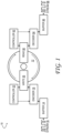
- FIG. 1 illustrates the 5D optical approach in schematic detail.
- FIG. 1 shows aspects of an example optical data storage and retrieval system 10.
- System 10 is configured to write and store data to substrate 12.
- the substrate may differ from one example to the next, but generally includes a transparent substrate.
- the substrate may be a polymer.
- the substrate may be an inorganic glass, such as silica glass.
- the substrate may take the form of a relatively thin optical layer (e.g ., 30 to 300 microns thick), coupled to a mechanically stable supporting layer.
- the substrate is shown in the form of rotating disk.
- the substrate may be shaped differently-as a translating slab or rotating cylinder, for instance.
- the substrate may be stationary with respect to the optical componentry of system 10.
- Buffer 14 of system 10 is configured to buffer an input data stream 16 to be written to the substrate.
- Encoder 18 parses the data from the buffer and provides appropriate control signal to write head 20, such that the data is written according to the desired encoding. Additional aspects of the encoding and write process are controlled by write controller 22, which may take the form of a computer system ( vide infra ) .
- FIG. 2 shows aspects of an example write head 20A of optical data storage and retrieval system 10.
- write head 20A includes a high-power, laser 24, an imaging optic in the form of an electronically addressable liquid-crystal spatial light modulator (LCSLM) 26A, and an electronically addressable polarization modulator (PM) 28.
- LCDMSLM liquid-crystal spatial light modulator
- PM electronically addressable polarization modulator
- Laser 24 is configured to emit a pulsed wavefront having uniform phase and polarization.
- the laser may be a femtosecond laser emitting in a narrow wavelength band of fixed ( e.g. , plane) polarization.
- Irradiance from the laser may comprise a repeating pulsetrain of sub-picosecond photon pulses- e.g ., tens to hundreds of femtoseconds in duration, for example.
- laser 24 may be one or more of Q-switched and mode-locked, to provide very brief pulses of very high energy.
- shorter wavelengths of a light maybe formed by using optical harmonic generators utilizing non-linear processes. Other forms of laser irradiance are also envisaged.
- the LCSLM 26A is configured as a dynamic digital hologram.
- the LCSLM includes an array of pixel elements that receive the wavefront from laser 24.
- the liquid crystal (LC) within each pixel element imparts a variable phase delay to the irradiance passing through that element.
- the phase delay is in a unique direction common to all pixel elements of the array.
- the magnitude of the variable phase delay may be controlled down to the pixel level.
- a phase delay imparted in the near field of the LCSLM creates an interference pattern in the far field, where substrate 12 is positioned.
- the far-field interference pattern may be controlled so as to irradiate each voxel of any layer of the substrate with the desired intensity.
- the holographic projection from LCSLM 26A passes through PM 28.
- the PM is a non-imaging active optic configured to rotate, by a controllably variable angle, the polarization state of the holographic projection.
- the holographic projection 'appears' as a parallel 2D array of write beams, each having controlled polarization and intensity, and each being mapped to a corresponding voxel of substrate 12.
- the mapping of LCSLM pixels to write beams i.e ., voxels
- the number of write beams achievable practically is about one-fourth the number of pixels on the LCSLM. For example, with about 10 million LCSLM pixels, one-million or more child beams may be formed.
- the array of write beams may be reconfigured at the full refresh rate of the LCSLM.
- State-of-the-art LCSLMs employing nematic liquid crystals have refresh rates of the order of 100 frames per second.
- LCSLM 26A and PM 28 are each coupled operatively to encoder 18.
- the encoder To the LCLSM, the encoder provides electronic signal that digitally defines the holographic projection; to the PM, the encoder provides electronic signal that defines the variable rotation applied to the polarization state of the holographic projection.
- the array of pixel positions of LCSLM 26A may be grouped into a plurality of non-overlapping or marginally overlapping holographic zones, which are exposed sequentially to the wavefront of laser 24.
- Each holographic zone may be a two-dimensional area of any desired shape- e.g ., rectangular, wedge-shaped, ring-shaped, etc.
- LCSLM 26A of system 10 may be coupled mechanically to a scanning stage 30, configured to change the relative positioning of the LCSLM versus the laser. In this manner, each of the holographic zones of the LCSLM may be irradiated in sequence.
- the scanning stage may be translational and/or rotational, and may be advanced a plurality of times (4, 9, 16 times, etc.
- write head 20A may include an adjustable objective lens system 32 configured to focus the irradiance of the write beams from the LCSLM to any selected depth layer of the substrate.
- write head 20A includes a LCSLM 26A in combination with a non-imaging PM 28.
- this LCSLM is used primarily to divide the laser wavefront into the required number of child beams, while the PM sets the rotation of the far-field polarization based on the data to be written.
- This enables a symbol S i to be written to each voxel i of the substrate, encoded by the slow-axis angle and retardance of that voxel.
- the symbol may be expressed as a digital value or bit sequence- e.g ., 00, 01, 10, 11. This can be achieved, for example by two different polarization angles and two possible retardance values for each angle. Other ways include the use of four polarization angles and a single retardance value. Naturally, a larger menu of polarization angles and/or retardance values would correspond to a longer bit sequence.
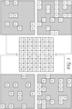
- write head 20A For each exposure of substrate 12, all of the voxels written to the substrate must have the same symbol S i . This is shown by example in FIG. 2 . Accordingly, if each voxel were to store two bits of information, four different write operations would be required. FIG. 3 illustrates and example sequence of exposures to achieve this, where an 8 x 8 voxel sector of data is written to the substrate in the likely case where the number of voxels assigned the same symbol is different for each exposure.
- write head 20A would need to compensate, in terms of laser power, for the variable number of voxels written during each exposure. This could be done, for instance, by splitting each of the indicated exposures into two or more smaller exposures, which would reduce throughput. Alternatively, it could be done by over-budgeting the laser power, requiring significant power from every exposure to be wasted. In sum, the unpredictability of the symbol distribution required for each exposure renders write head 20A inefficient in terms of bandwidth and/or optical power utilization.
- a modified write head for optical data storage and retrieval system 10 and associated modes of parallel data writing.
- these examples use an LCSLM to divide the laser irradiance into numerous voxel-sized child beams and simultaneously control the polarization of each of the child beams. This is achieved without using multiple active modulators, which would increase cost and complexity and reduce throughput or efficiency, as described above.
- the modified write head operates based on the principle that shifting a grating or a hologram spatially causes its far field to change phase.
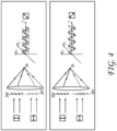
- FIG. 4 shows a first grating 34X and an adjacent second grating 34Y of the same frequency, or pitch.
- the two gratings each image the incident wavefront onto a single spot 36, which may correspond to a single substrate voxel.
- gratings 34X and 34Y are irradiated by light of different polarizations- e.g ., the vertical and horizontal plane polarizations indicated by the boxed arrows of FIG. 4 -then, by controlling the phase and intensity of the two superimposed beams, the polarization as well as the amplitude of the resultant irradiance of spot 36 may be controlled.
- the configuration of FIG. 4 may have certain practical limitations.
- grating 34X into numerous component gratings with the same diffraction properties
- divide grating 34Y in the same way, and comingle the component gratings over a suitably small length scale.
- Tiles of grating 34X would be irradiated with one polarization state, and tiles of grating 34Y would be illuminated with another polarization state. In this approach, it would be necessary to irradiate different regions of the LCSLM with different polarized beams.
- this may be achieved using a polarization-modulating sheet arranged between the laser and the LCSLM.
- the polarization-modulating sheet may comprise an alternating tiling of cells arranged in registry with the pixel elements of the array, each cell configured to rotate the polarization of a portion of the wavefront passing through that cell.
- a single LCSLM is used to control both phase and polarization, down to the pixel level. This operation is within the ability of a suitably configured LCSLM, and is enacted by write head 20B of FIG. 5 .
- the array of pixel elements of LCSLM 26 of FIG. 5 is configured to modulate the phase and polarization of different portions of the wavefront by different amounts, and to diffract light from the different portions to a substrate with writeable optical properties.
- the LCSLM is configured to modulate the different portions of the wavefront to different near-field polarizations and to image the light to an array of substrate voxels at different far-field polarizations.
- the encoder logic is configured to receive data and to control modulation of the phase and polarization such that the light diffracted from the imaging optic writes the data to the substrate.
- data may include inequivalent first and second data values written simultaneously by the light diffracted from the imaging optic.
- the first data value may be written to a first voxel by light of a first far-field polarization while the second data value is written to a second voxel by light of a second, inequivalent far-field polarization.
- Control of two different parameters may be effected independently or with correlation.
- the more straightforward mode of controlling both phase and polarization is to control each parameter independently. This may be achieved via an LCSLM in which the various pixel elements are addressable to modulate phase, and independently addressable to modulate polarization.
- the LCSLM is configured to provide two independent degrees of freedom in the nematic director. Rotation in one direction affects phase and the other polarization.
- FIG. 6 shows aspects of a state-of-the-art, single-axis LCSLM 26A.
- a state-of-the-art LC LCSLM includes one independently addressable electrode 38 per pixel element.
- a controllable voltage V ij is applied to this electrode via a thin-layer transistor (TFT) arranged at the intersection of every row i and column j of pixel elements.
- V ij controls the magnitude of the external electric field to which the LC molecules 40 of the pixel element are subject.
- the electric field has a variable magnitude but a fixed direction, which is the same for all pixel elements of the LCSLM array.
- the electric field orients the LC molecules of a given pixel element in one direction only, to a greater or lesser degree depending on the voltage applied to the electrode.
- This provides a variable phase delay of the polarization component aligned parallel to the major axis of the oriented LC molecules, which, again, is the same for every pixel element of the array.
- a modified LCSLM has two or more independently addressable electrodes per pixel element.
- An example of such an LCSLM is described in U.S. Patent Application Number 15/623,906 .
- the two independently addressable electrodes 42 and 44 of LCSLM 26B are biased independently of the other by a pair of TFTs arranged at each intersection.
- a first controllable voltage V ij is applied to electrode 42, and a second controllable voltage U ij is applied to electrode 44.
- the average of V ij and U ij , relative to the voltage V 0 of common electrode 46 determines the magnitude of the electric field in the transmission direction, while the absolute difference between V ij and U ij determines the magnitude of the electric field in a direction substantially orthogonal to the transmission direction.
- V ij and U ij When voltages V ij and U ij are applied, a controllable portion of the LC molecules align in the transmission direction, and another controllable portion in the orthogonal direction. This condition enables different amounts of phase delay to be imparted independently in two, substantially orthogonal directions. Moreover, these different amounts may be varied from one pixel to the next.
- independently addressable electrodes may be arranged such that the electric field that orients the LC molecules may have a controllably variable direction as well as a controllably variable magnitude.
- modified LCSLM 26B enables each pixel to modulate the phase of the wavefront for X and Y polarization components independently.
- the modified LCSLM can variably rotate as well as variably retard each portion of the wavefront independently, controlled by the voltages V ij and U ij applied to the independently addressable electrodes.
- the average voltage applied to the electrodes affects the phase delay of a first component of the portion of the wavefront passing through the associated element, while the differential voltage V ij - U ij affects the phase of a non-parallel ( e.g ., orthogonal) second component of the portion of the wavefront.
- LCSLM 26B may be used to achieve independent (i.e., uncorrelated) pixel-wise control of phase and polarization, which lends itself to operationally straightforward, parallel data writing.
- correlated control of these parameters is the basis of another useful data-writing mode.
- correlated control may be achieved using a simpler LCSLM 26A, which provides only one depth-of-field per pixel.
- LCSLM 26A may be programmed to simultaneously project two different, but interrelated holograms: one representing phase retardance for horizontal polarization, the other representing phase retardance for vertical polarization.
- the required programming may be enacted by the logic of encoder 18, which is configured to execute a holographic-design algorithm to control modulation of the phase and polarization.
- the modifications recognize (a) that two different holograms are to be projected from each area of the LCSLM, for modulation of the two polarization states; (b) that each pixel of the LCSLM simultaneously modulates both phase and polarization; and (c) that there may be an infinite number of combinations of spot phases suitable for achieving the desired polarization at a given spot.
- Suitable input for the holographic-design algorithm includes the position, polarization, and amplitude for each voxel of an imaged depth layer of the substrate.
- the algorithm transforms this holographic content into a matrix of scalar electric field components for X and Y polarizations. In doing so, the algorithm optimizes the voltage V(x,y) applied to each pixel element of the LCSLM to minimize the errors in polarization and phase (as no one pixel can provide independent control of polarization and phase).
- FIG. 8 illustrates an example holographic-design method 48 based on a modified Gerchberg-Saxton (GS) algorithm.
- a target output plane is created.
- the target output plane consists of the amplitude of the electric field in the horizontal (
- the vertical electric-field amplitude E v is set equal to the target amplitude for the vertical polarization state, for a randomly selected phase.
- the horizontal electric-field amplitude E h is set equal to the target amplitude for the horizontal polarization, with a phase less than E v + ⁇ VH .
- H h IFT(E h )
- H v IFT(E v )
- IFT stands for Inverse Fourier Transform
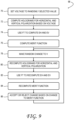
- FIG. 9 illustrates an example holographic-design method 68 based on a modified Direct Binary Search (DBS) or 'simulated-annealing' algorithm.
- the voltage matrix V(x,y) is set to a randomly selected value.
- a merit function is computed.
- a random change to V(x,y) is made.
- At 80 are computed H v and H h .
- At 82 are computed E v and E h .
- a new merit function is computed.
- the random change made to V(x,y) is accepted or rejected in a probabilistic manner, based on whether the merit function has improved. Execution of algorithm 68 then returns to 78.
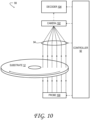
- read head 90 of optical data storage and retrieval system 10 reads the data that has been stored on substrate 12 according to parameters supplied by read controller 92. The read data is then passed to decoder 94, which decodes and outputs the data to read buffer 96, from which output stream 98 is made available.
- FIG. 10 shows aspects of an example read head 90.
- the read head includes a polarized optical probe 100 and an analyzer camera 102.
- the polarized optical probe may include a low-power diode laser or other polarized light source.
- Read controller 92 is coupled operatively to the polarized optical probe and configured to control the angle of the polarization plane of emission of the polarized optical probe.
- Analyzer camera 102 may include a high-resolution / high frame-rate CMOS or other suitable photodetector array.
- the analyzer camera is configured to image light from polarized optical probe 100, after such light has interacted with the voxels of substrate 12.
- FIG. 10 shows transmission of polarized light rays through the medium and on to the camera, the light rays may, in alternative configurations, reach the camera by reflection from the medium.
- Each image frame acquired by analyzer camera 102 may include a plurality of component images captured simultaneously or in rapid succession.
- the analyzer camera may resolve, in corresponding pixel arrays of the component images, localized intensity in different polarization planes.
- the analyzer camera may include switchable or tunable polarization control in the form of a liquid-crystal retarder or Pockels cell, for example.
- four images of each target portion of substrate 12 are acquired in sequence by the analyzer camera as the polarized optical probe 100 is rotated through four different polarization angles. This process is akin to measuring basis vectors of a multi-dimensional vector, where here the 'vector' captures the birefringent properties of the voxels of the imaged target portion.
- a background image is also acquired, which captures the distribution of sample-independent polarization noise in the component images.
- read head 90 may include an adjustable collection lens system 104.
- the adjustable collection lens system may collect light rays diffracted from a selected depth layer of the optical storage medium, and reject other light rays.
- lensless imaging based on interferometry may be employed.
- data decoder 94 is configured to receive the component images from analyzer camera 102 and to enact the image processing necessary to retrieve the data stored in substrate 12. Such data may be decoded according to a machine-learned method and/or a canonical method in which an observable physical property is connected through one or more intermediates to the data read from the substrate.
- LCSLMs described above are indeed suitable for modulating the phase and polarization of different portions of a wavefront by different amounts, and diffracting light from the different portions to a substrate
- imaging optics of other types may also be suitable.
- optical data storage has been described in the context of an integrated read-write system (optical data storage and retrieval system 10), this disclosure is also consonant with various write-only systems in which data is written to a data-storage substrate that may be removed from the system and read elsewhere.
- the methods and processes described herein may be tied to a computer system of one or more computing devices.
- such methods and processes may be implemented as a computer-application program or service, an application-programming interface (API), a library, and/or other computer-program product.
- API application-programming interface
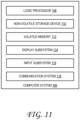
- FIG. 11 schematically shows a non-limiting embodiment of a computer system 106 that can enact one or more of the methods and processes described above.
- Computer system 106 is shown in simplified form.
- Computer system 106 may take the form of one or more bench-top or server computers and/or dedicated electronic controllers.
- Encoder 18, controllers 22 and 92, and decoder 94 are examples of a computer system 106.
- Computer system 106 includes a logic processor 108 volatile memory 112, and a non-volatile storage device 110.
- Computer system 106 may optionally include a display subsystem 114, input subsystem 116, communication subsystem 118, and/or other components not shown in FIG. 10 .
- Logic processor 108 includes one or more physical devices configured to execute instructions.
- the logic processor may be configured to execute instructions that are part of one or more applications, programs, routines, libraries, objects, components, data structures, or other logical constructs. Such instructions may be implemented to perform a task, implement a data type, transform the state of one or more components, achieve a technical effect, or otherwise arrive at a desired result.
- the logic processor may include one or more physical processors (hardware) configured to execute software instructions. Additionally or alternatively, the logic processor may include one or more hardware logic circuits or firmware devices configured to execute hardware-implemented logic or firmware instructions. Processors of the logic processor 108 may be single-core or multi-core, and the instructions executed thereon may be configured for sequential, parallel, and/or distributed processing. Individual components of the logic processor optionally may be distributed among two or more separate devices, which may be remotely located and/or configured for coordinated processing. Aspects of the logic processor may be virtualized and executed by remotely accessible, networked computing devices configured in a cloud-computing configuration. In such a case, these virtualized aspects are run on different physical logic processors of various different machines, it will be understood.
- Non-volatile storage device 110 includes one or more physical devices configured to hold instructions executable by the logic processors to implement the methods and processes described herein. When such methods and processes are implemented, the state of non-volatile storage device 110 may be transformed- e.g ., to hold different data.
- Non-volatile storage device 110 may include physical devices that are removable and/or built-in.
- Non-volatile storage device 110 may include optical memory (e.g ., CD, DVD, HD-DVD, Blu-Ray Disc, etc. ), semiconductor memory (e.g., ROM, EPROM, EEPROM, FLASH memory, etc .), and/or magnetic memory (e.g., hard-disk drive, floppy-disk drive, tape drive, MRAM, etc. ) , or other mass storage device technology.
- Non-volatile storage device 110 may include nonvolatile, dynamic, static, read/write, read-only, sequential-access, location-addressable, file-addressable, and/or content-addressable devices. It will be appreciated that non-volatile storage device 110 is configured to hold instructions even when power is cut to the non-volatile storage device 110.
- Volatile memory 112 may include physical devices that include random access memory. Volatile memory 112 is typically utilized by logic processor 108 to temporarily store information during processing of software instructions. It will be appreciated that volatile memory 112 typically does not continue to store instructions when power is cut to the volatile memory 112.
- logic processor 108 volatile memory 112, and non-volatile storage device 110 may be integrated together into one or more hardware-logic components.
- hardware-logic components may include field-programmable gate arrays (FPGAs), program- and application-specific integrated circuits (PASIC / ASICs), program- and application-specific standard products (PSSP / ASSPs), system-on-a-chip (SOC), and complex programmable logic devices (CPLDs), for example.
- FPGAs field-programmable gate arrays
- PASIC / ASICs program- and application-specific integrated circuits
- PSSP / ASSPs program- and application-specific standard products
- SOC system-on-a-chip
- CPLDs complex programmable logic devices
- display subsystem 114 may be used to present a visual representation of data held by non-volatile storage device 110.
- the visual representation may take the form of a graphical user interface (GUI).
- GUI graphical user interface
- the state of display subsystem 114 may likewise be transformed to visually represent changes in the underlying data.
- Display subsystem 114 may include one or more display devices utilizing virtually any type of technology. Such display devices may be combined with logic processor 108, volatile memory 112, and/or non-volatile storage device 110 in a shared enclosure, or such display devices may be peripheral display devices.
- input subsystem 116 may comprise or interface with one or more user-input devices such as a keyboard, mouse, touch screen, etc.
- communication subsystem 118 may be configured to communicatively couple various computing devices described herein with each other, and with other devices.
- Communication subsystem 118 may include wired and/or wireless communication devices compatible with one or more different communication protocols.
- the communication subsystem may be configured for communication via a wireless telephone network, or a wired or wireless local- or wide-area network, such as a HDMI over Wi-Fi connection.
- the communication subsystem may allow computer system 106 to send and/or receive messages to and/or from other devices via a network such as the Internet.
Landscapes
- Physics & Mathematics (AREA)
- Optics & Photonics (AREA)
- General Physics & Mathematics (AREA)
- Mathematical Physics (AREA)
- Optical Recording Or Reproduction (AREA)
- Holo Graphy (AREA)
- Liquid Crystal (AREA)
Description
- High-power, short-pulse laser irradiance can be used to write and store data within a glass substrate. The irradiance induces a long-lived lattice perturbation at its focus, which derives from non-linear, two-photon absorption by the substrate. In some cases, the lattice perturbation has the optical properties of a nano-grating embedded within the substrate at the point where the irradiance is imaged. Data written to a glass substrate in this manner can be read back using a polarized optical beam to interrogate the various grating-like perturbations formed within it.
JP 2014 211935 A irradiation system 4 records the information on therecording medium 2 as a three-dimensional optical anisotropy distribution by irradiating therecording medium 2 having photosensitivity with the signal light and the reference light.
Masanori Takabayashi et al., "Self-referential holography and its applications to data storage and phase-to-intensity conversion", OPTICS EPRESS 3669, Vol. 21, No. 3., 6 February 2013 describes that holographic recording methods require the use of a reference beam that is coherent with the signal beam carrying the information to be recorded. In this paper, we propose self-referential holography (SRH) for holographic recording without the use of a reference beam. SRH can realize purely one-beam holographic recording by considering the signal beam itself as the reference beam. The readout process in SRH is based on energy transfer by inter-pixel interference in holographic diffraction, which depends on the spatial phase difference between the recorded phase and the readout phase. The phase-modulated recorded signal is converted into an intensity-modulated beam that can be easily detected using a conventional image sensor. SRH can be used effectively for holographic data storage and phase-to-intensity conversion.
US 2001/002895 A1 describes that an optical storage medium of the present invention enables storage of data with high precision at high speed, and rewriting of data at high speed without an erasing process. Optical storage, reading and retrieving methods and optical storage, reading, and retrieving apparatuses using the medium are also provided. The optical storage medium has at least a polarization-sensitive member having the photo-induced birefringence property, such as a member made of polyester polymer having cyanoazobenzene as a side chain. The above apparatuses have spatial light modulator capable of modulating polarization. The modulator provides information of bit of two-dimensional data to each corresponding pixel by application or non-application of a voltage, and modulates the polarization of the beam incident on each pixel. Thereby, a signal beam transmitted through the spatial light modulator having a spatial polarization modulation corresponding to the two-dimensional data is obtained. The signal beam illuminates the optical storage medium, and at the same time, a reference beam illuminates the same region in the medium where the signal beam illuminates. Thus a hologram of the polarization modulation of the signal beam corresponding to the two-dimensional data is stored in the optical storage medium.
EP 1 550 922 A1
US 6 483 735 B1 describes that three-, and four-dimensional ("3-D" and "4-D") volume radiation memories store multiple binary bits of information-typically about five to ten and more typically eight such bits-in the same physical volumes on several different photochromic chemicals co-located in the volume. Each of the multiple photochromic chemicals is individually selectively written with an individually associated pair of radiation beams of an appropriate combined frequency-i.e., a "color"-and energy by a process of two-photon ("2-P") absorption. All the multiple information bits that are stored within all the photochromic chemicals in each addressable domain are read in common, and induced to simultaneously fluoresce, again by process of 2-P absorption. The fluorescence of each of different photochromic chemical in each addressed domain-which fluorescence is selective in accordance with the written state of each such photochromic chemical-is separated from, and is separately detected from, the fluorescence of all other photochromic chemicals because it is of a unique color, and is spatially steered to an associated detector array, normally a Charge Coupled Device (CCD), by a monochromator, normally a prism. Exemplary fluorescent photochromic chemicals are spirobenzopyran, rhodamine, cumarin and anthracene. Suitable groups of photochromic chemicals are formed from individual photochromic chemicals exhibiting narrow, sharp, separate spectra of absorption and of emission suitably distinct from each other, and where no chemical's fluorescent emission energy overlaps the absorption energies of any other chemicals.
US 2016/365107 A1 describes that in recording technologies for batch formation of a plurality of recording bits in a recording medium by forming a plurality of optical spots using an ultrashort pulse laser and a spatial optical modulator, the hatch recordable hit number has an upper limit, resulting in restricted recording speed. The intensity of the optical spot is corrected to increase the batch recordable bit number for increasing the recording speed.
JP 2002 298378 A signal light 1 holding a first data group by an intensity distribution 25 and holding a second data group by apolarization distribution 26 is irradiated onto a predetermined area of an optical recording medium simultaneously with a reference light.Polarization distribution 26 and intensity distribution 25 ofsignal light 1 is multiplex-recorded as a hologram. As described above, by simultaneously recording a plurality of data groups on the optical recording medium, it is possible to significantly increase the speed as compared with the related art. - According to aspects of the present invention there is provided a system as defined in the accompanying claims.
- The examples disclosed herein relate to an optical data-storage system, comprising a laser, an imaging optic, and associated computer logic. The laser is configured to emit a pulsed wavefront having uniform phase and polarization. The imaging optic is configured to modulate the phase and polarization of different portions of the wavefront by different amounts, and to diffract light from the different portions to a substrate with writeable optical properties. The logic is configured to receive data and to control modulation of the phase and polarization such that the light diffracted from the imaging optic writes the data to the substrate.
- This Summary is provided to introduce a selection of concepts in a simplified form that are further described below in the Detailed Description.
-
-
FIG. 1 shows aspects of an example optical data-storage and retrieval system. -
FIG. 2 shows aspects of an example write head of an optical data-storage and retrieval system comprising separate polarization and phase modulation stages. -
FIG. 3 schematically illustrates an 8 x 8 voxel sector having four different symbol values written in four consecutive exposures of a substrate, each exposure writing symbols of the same value. -
FIG. 4 schematically illustrates the concept of two offset gratings imaging to the same spot on a substrate, each grating contributing far-field polarization as well as phase information. -
FIG. 5 shows aspects of another example write head of an optical data-storage and retrieval system achieving concerted polarization and phase modulation. -
FIGS. 6 and 7 show aspects of example liquid-crystal spatial light modulators (LCSLMs). -
FIGS. 8 and9 illustrate example holographic-design methods. -
FIG. 10 shows aspects of an example read head of an optical data-storage and retrieval system. -
FIG. 11 shows aspects of an example computer system. - This disclosure is presented by way of example, and with reference to the drawing figures listed above. Components, process steps, and other elements that may be substantially the same in one or more of the figures are identified coordinately and described with minimal repetition. It will be noted, however, that elements identified coordinately may also differ to some degree. It will be further noted that the figures are schematic and generally not drawn to scale. Rather, the various drawing scales, aspect ratios, and numbers of components shown in the figures may be purposely distorted to make certain features or relationships easier to see.
- As described above, data can be written to a glass or other solid substrate using high-power, coherent irradiance. The term 'voxel' is used herein to refer to any discrete locus of a substrate where an individual data value (i.e., symbol) may be stored. The data stored in a voxel may take various forms. In principle, any of the Muller-matrix coefficients of the substrate lattice can be manipulated to encode data. In examples using silica glass substrates, the lattice perturbation from focused, polarized irradiance takes the form of a non-native birefringence localized at the focus. Accordingly, each voxel of the substrate may be modeled as a very small waveplate of a retardance δd and slow-axis orientation ϕ. These model parameters may be manipulated independently to write a desired symbol to a given voxel. Here, the polarization angle of the beam determines the slow-axis orientation ϕ, while the amplitude of the beam determines the strength of the waveplate grating, and therefore the retardance δd.
- By dividing the continuous space of achievable slow-axis orientations and retardances into discrete intervals, multi-bit data values may be encoded into each voxel-viz., by independently coercing the birefringence of that voxel to be within one of the discrete intervals. In this manner, each voxel may encode one of R ≥ 1 different retardance states at each of Q ≥ 1 different polarization angles. In some examples, many parallel layers of voxel structures may be written to the same substrate by focusing the laser irradiance to specified depths below the irradiated surface of the substrate. This mode of data storage is referred to as '5D optical storage'.
- In order to write data at an acceptably high throughput, numerous voxels may be written in parallel. Although it is possible to write each voxel serially, the required overhead of high-speed, high-precision mechanical movement may make such an approach impractical. To write data in parallel, the output of a high-power laser may be split into a plurality of independently modulated, voxel-sized child beams, so that a corresponding plurality of voxels may be written simultaneously. Each child beam, however, must be rotated to the particular polarization state appropriate for the symbol it writes.
-
FIG. 1 illustrates the 5D optical approach in schematic detail.FIG. 1 shows aspects of an example optical data storage andretrieval system 10.System 10 is configured to write and store data tosubstrate 12. The substrate may differ from one example to the next, but generally includes a transparent substrate. In some examples, the substrate may be a polymer. In some examples, the substrate may be an inorganic glass, such as silica glass. In some examples, the substrate may take the form of a relatively thin optical layer (e.g., 30 to 300 microns thick), coupled to a mechanically stable supporting layer. InFIG. 1 and subsequent drawings, the substrate is shown in the form of rotating disk. In other examples, the substrate may be shaped differently-as a translating slab or rotating cylinder, for instance. In some examples, the substrate may be stationary with respect to the optical componentry ofsystem 10.Buffer 14 ofsystem 10 is configured to buffer aninput data stream 16 to be written to the substrate.Encoder 18 parses the data from the buffer and provides appropriate control signal to writehead 20, such that the data is written according to the desired encoding. Additional aspects of the encoding and write process are controlled bywrite controller 22, which may take the form of a computer system (vide infra). -
FIG. 2 shows aspects of anexample write head 20A of optical data storage andretrieval system 10. To enable simultaneous, parallel writing, writehead 20A includes a high-power,laser 24, an imaging optic in the form of an electronically addressable liquid-crystal spatial light modulator (LCSLM) 26A, and an electronically addressable polarization modulator (PM) 28. -
Laser 24 is configured to emit a pulsed wavefront having uniform phase and polarization. The laser may be a femtosecond laser emitting in a narrow wavelength band of fixed (e.g., plane) polarization. Irradiance from the laser may comprise a repeating pulsetrain of sub-picosecond photon pulses-e.g., tens to hundreds of femtoseconds in duration, for example. In some implementations,laser 24 may be one or more of Q-switched and mode-locked, to provide very brief pulses of very high energy. In some cases, shorter wavelengths of a light maybe formed by using optical harmonic generators utilizing non-linear processes. Other forms of laser irradiance are also envisaged. -
LCSLM 26A is configured as a dynamic digital hologram. The LCSLM includes an array of pixel elements that receive the wavefront fromlaser 24. The liquid crystal (LC) within each pixel element imparts a variable phase delay to the irradiance passing through that element. In a state-of-the-art LCSLM, the phase delay is in a unique direction common to all pixel elements of the array. Because each pixel element is independently addressable, the magnitude of the variable phase delay may be controlled down to the pixel level. As with any grating, a phase delay imparted in the near field of the LCSLM creates an interference pattern in the far field, wheresubstrate 12 is positioned. By controlling the near-field phase delay from each pixel element of the LCSLM, the far-field interference pattern may be controlled so as to irradiate each voxel of any layer of the substrate with the desired intensity. - In
write head 20A ofFIG. 2 , the holographic projection fromLCSLM 26A passes throughPM 28. The PM is a non-imaging active optic configured to rotate, by a controllably variable angle, the polarization state of the holographic projection. To the substrate, therefore, the holographic projection 'appears' as a parallel 2D array of write beams, each having controlled polarization and intensity, and each being mapped to a corresponding voxel ofsubstrate 12. It will be noted that the mapping of LCSLM pixels to write beams (i.e., voxels) is not necessarily a 1:1 mapping, but may be 2:1, 4:1, or 10:1, among other suitable mappings. In some examples, the number of write beams achievable practically is about one-fourth the number of pixels on the LCSLM. For example, with about 10 million LCSLM pixels, one-million or more child beams may be formed. Moreover, the array of write beams may be reconfigured at the full refresh rate of the LCSLM. State-of-the-art LCSLMs employing nematic liquid crystals have refresh rates of the order of 100 frames per second. - In
write head 20A,LCSLM 26A andPM 28 are each coupled operatively toencoder 18. To the LCLSM, the encoder provides electronic signal that digitally defines the holographic projection; to the PM, the encoder provides electronic signal that defines the variable rotation applied to the polarization state of the holographic projection. - In some implementations, the array of pixel positions of
LCSLM 26A may be grouped into a plurality of non-overlapping or marginally overlapping holographic zones, which are exposed sequentially to the wavefront oflaser 24. Each holographic zone may be a two-dimensional area of any desired shape-e.g., rectangular, wedge-shaped, ring-shaped, etc. Accordingly,LCSLM 26A ofsystem 10 may be coupled mechanically to ascanning stage 30, configured to change the relative positioning of the LCSLM versus the laser. In this manner, each of the holographic zones of the LCSLM may be irradiated in sequence. The scanning stage may be translational and/or rotational, and may be advanced a plurality of times (4, 9, 16 times, etc.) for each time that the LCSLM is addressed. This approach effectively multiplies the temporal bandwidth of the LCSLM beyond its maximum refresh rate. Nevertheless, the laser, LCSLM, PM, and substrate may be fixed in position in some examples. In examples in which data is to be written to a plurality of depth layers ofsubstrate 12,write head 20A may include an adjustableobjective lens system 32 configured to focus the irradiance of the write beams from the LCSLM to any selected depth layer of the substrate. - In the configuration described above, write
head 20A includes aLCSLM 26A in combination with anon-imaging PM 28. As noted above, this LCSLM is used primarily to divide the laser wavefront into the required number of child beams, while the PM sets the rotation of the far-field polarization based on the data to be written. This enables a symbol Si to be written to each voxel i of the substrate, encoded by the slow-axis angle and retardance of that voxel. The symbol may be expressed as a digital value or bit sequence-e.g., 00, 01, 10, 11. This can be achieved, for example by two different polarization angles and two possible retardance values for each angle. Other ways include the use of four polarization angles and a single retardance value. Naturally, a larger menu of polarization angles and/or retardance values would correspond to a longer bit sequence. - One disadvantage of
write head 20A is that for each exposure ofsubstrate 12, all of the voxels written to the substrate must have the same symbol Si. This is shown by example inFIG. 2 . Accordingly, if each voxel were to store two bits of information, four different write operations would be required.FIG. 3 illustrates and example sequence of exposures to achieve this, where an 8 x 8 voxel sector of data is written to the substrate in the likely case where the number of voxels assigned the same symbol is different for each exposure. - To enact the write sequence of
FIG. 3 , writehead 20A would need to compensate, in terms of laser power, for the variable number of voxels written during each exposure. This could be done, for instance, by splitting each of the indicated exposures into two or more smaller exposures, which would reduce throughput. Alternatively, it could be done by over-budgeting the laser power, requiring significant power from every exposure to be wasted. In sum, the unpredictability of the symbol distribution required for each exposure renderswrite head 20A inefficient in terms of bandwidth and/or optical power utilization. - Thus, described in further detail below are examples related to a modified write head for optical data storage and
retrieval system 10 and associated modes of parallel data writing. Briefly, these examples use an LCSLM to divide the laser irradiance into numerous voxel-sized child beams and simultaneously control the polarization of each of the child beams. This is achieved without using multiple active modulators, which would increase cost and complexity and reduce throughput or efficiency, as described above. The modified write head operates based on the principle that shifting a grating or a hologram spatially causes its far field to change phase. - Conceptually, the present approach is akin to the writing mode illustrated in
FIG. 4. FIG. 4 shows a first grating 34X and an adjacent second grating 34Y of the same frequency, or pitch. The two gratings each image the incident wavefront onto asingle spot 36, which may correspond to a single substrate voxel. Significantly, ifgratings FIG. 4 -then, by controlling the phase and intensity of the two superimposed beams, the polarization as well as the amplitude of the resultant irradiance ofspot 36 may be controlled. - The configuration of
FIG. 4 may have certain practical limitations. First, although the beams fromgratings spot 36, they differ from each other in angle space. Accordingly, as the beam expands again, downstream of 36, the polarization content will again separate. For some data-writing applications, this effect may have undesirable resolution-limiting consequences related to reduction in the effective aperture size and numerical aperture. - One way to address this limitation is to divide grating 34X into numerous component gratings with the same diffraction properties, divide grating 34Y in the same way, and comingle the component gratings over a suitably small length scale. This could be done, for instance, using an LCSLM optoelectronically 'tiled' with alternating portions of
gratings - In examples according to the claimed invention, to avoid aperture-size reduction, but without requiring piece-wise illumination of the LCSLM, a single LCSLM is used to control both phase and polarization, down to the pixel level. This operation is within the ability of a suitably configured LCSLM, and is enacted by
write head 20B ofFIG. 5 . The array of pixel elements ofLCSLM 26 ofFIG. 5 is configured to modulate the phase and polarization of different portions of the wavefront by different amounts, and to diffract light from the different portions to a substrate with writeable optical properties. In particular, the LCSLM is configured to modulate the different portions of the wavefront to different near-field polarizations and to image the light to an array of substrate voxels at different far-field polarizations. To this end, the encoder logic is configured to receive data and to control modulation of the phase and polarization such that the light diffracted from the imaging optic writes the data to the substrate. Such data may include inequivalent first and second data values written simultaneously by the light diffracted from the imaging optic. In other words, the first data value may be written to a first voxel by light of a first far-field polarization while the second data value is written to a second voxel by light of a second, inequivalent far-field polarization. - Control of two different parameters may be effected independently or with correlation. Conceptually, the more straightforward mode of controlling both phase and polarization is to control each parameter independently. This may be achieved via an LCSLM in which the various pixel elements are addressable to modulate phase, and independently addressable to modulate polarization. In other words, the LCSLM is configured to provide two independent degrees of freedom in the nematic director. Rotation in one direction affects phase and the other polarization.
-
FIG. 6 shows aspects of a state-of-the-art, single-axis LCSLM 26A. The skilled reader will appreciate that a state-of-the-art LC LCSLM includes one independentlyaddressable electrode 38 per pixel element. A controllable voltage Vij is applied to this electrode via a thin-layer transistor (TFT) arranged at the intersection of every row i and column j of pixel elements. Vij controls the magnitude of the external electric field to which theLC molecules 40 of the pixel element are subject. The electric field has a variable magnitude but a fixed direction, which is the same for all pixel elements of the LCSLM array. Accordingly, the electric field orients the LC molecules of a given pixel element in one direction only, to a greater or lesser degree depending on the voltage applied to the electrode. This provides a variable phase delay of the polarization component aligned parallel to the major axis of the oriented LC molecules, which, again, is the same for every pixel element of the array. - In examples according to the claimed invention, a modified LCSLM has two or more independently addressable electrodes per pixel element. An example of such an LCSLM is described in
U.S. Patent Application Number 15/623,906 . As shown schematically inFIG. 7 , the two independentlyaddressable electrodes LCSLM 26B are biased independently of the other by a pair of TFTs arranged at each intersection. A first controllable voltage Vij is applied toelectrode 42, and a second controllable voltage Uij is applied toelectrode 44. In this configuration, the average of Vij and Uij, relative to the voltage V0 ofcommon electrode 46 determines the magnitude of the electric field in the transmission direction, while the absolute difference between Vij and Uij determines the magnitude of the electric field in a direction substantially orthogonal to the transmission direction. When voltages Vij and Uij are applied, a controllable portion of the LC molecules align in the transmission direction, and another controllable portion in the orthogonal direction. This condition enables different amounts of phase delay to be imparted independently in two, substantially orthogonal directions. Moreover, these different amounts may be varied from one pixel to the next. In other configurations, independently addressable electrodes may be arranged such that the electric field that orients the LC molecules may have a controllably variable direction as well as a controllably variable magnitude. - In effect, the pixel configuration of modified
LCSLM 26B enables each pixel to modulate the phase of the wavefront for X and Y polarization components independently. Thus, if the incoming wavefront is plane polarized, the modified LCSLM can variably rotate as well as variably retard each portion of the wavefront independently, controlled by the voltages Vij and Uij applied to the independently addressable electrodes. In particular, the average voltage applied to the electrodes affects the phase delay of a first component of the portion of the wavefront passing through the associated element, while the differential voltage Vij - Uij affects the phase of a non-parallel (e.g., orthogonal) second component of the portion of the wavefront. - As noted above,
LCSLM 26B, may be used to achieve independent (i.e., uncorrelated) pixel-wise control of phase and polarization, which lends itself to operationally straightforward, parallel data writing. However, correlated control of these parameters is the basis of another useful data-writing mode. Moreover, correlated control may be achieved using asimpler LCSLM 26A, which provides only one depth-of-field per pixel. - To this end,
LCSLM 26A may be programmed to simultaneously project two different, but interrelated holograms: one representing phase retardance for horizontal polarization, the other representing phase retardance for vertical polarization. The required programming may be enacted by the logic ofencoder 18, which is configured to execute a holographic-design algorithm to control modulation of the phase and polarization. Generally, the modifications recognize (a) that two different holograms are to be projected from each area of the LCSLM, for modulation of the two polarization states; (b) that each pixel of the LCSLM simultaneously modulates both phase and polarization; and (c) that there may be an infinite number of combinations of spot phases suitable for achieving the desired polarization at a given spot. - Suitable input for the holographic-design algorithm includes the position, polarization, and amplitude for each voxel of an imaged depth layer of the substrate. The algorithm transforms this holographic content into a matrix of scalar electric field components for X and Y polarizations. In doing so, the algorithm optimizes the voltage V(x,y) applied to each pixel element of the LCSLM to minimize the errors in polarization and phase (as no one pixel can provide independent control of polarization and phase).
-
FIG. 8 illustrates an example holographic-design method 48 based on a modified Gerchberg-Saxton (GS) algorithm. At 50 ofmethod 48, a target output plane is created. The target output plane consists of the amplitude of the electric field in the horizontal (|Eh_target|) and vertical (|Ev_target|) polarization states and the phase difference ΔθVH between the two polarization states. At 52 the vertical electric-field amplitude Ev is set equal to the target amplitude for the vertical polarization state, for a randomly selected phase. At 54 the horizontal electric-field amplitude Eh is set equal to the target amplitude for the horizontal polarization, with a phase less than Ev + ΔθVH. At 56 a hologram for the two polarization states is found using an inverse Fourier-transform function-viz., Hh = IFT(Eh), Hv = IFT(Ev) where IFT stands for Inverse Fourier Transform At 58, for each pixel of Hh and Hv, a refined pixel voltage V is found that minimizes the pixel error. At 60 the found holograms are refined to Hh' and Hv' using the selected voltages. At 62 the actual electric-field reconstruction of the two holograms, Eh' and Ev', is found using a Fourier transform (FT). At 64 a new phase and amplitude for Ev and Eh are selected using Eh', Ev', and ΔθVH. Execution ofmethod 40 then returns to 56. -
FIG. 9 illustrates an example holographic-design method 68 based on a modified Direct Binary Search (DBS) or 'simulated-annealing' algorithm. At 70 ofmethod 68, the voltage matrix V(x,y) is set to a randomly selected value. At 72 is computed Hv = f(V) and Hh = f(V). At 74 is computed Eh and Ev using an FT. At 76 a merit function is computed. At 78 a random change to V(x,y) is made. At 80 are computed Hv and Hh. At 82 are computed Ev and Eh. At 84, a new merit function is computed. At 86, the random change made to V(x,y) is accepted or rejected in a probabilistic manner, based on whether the merit function has improved. Execution ofalgorithm 68 then returns to 78. - Returning briefly to
FIG. 1 , readhead 90 of optical data storage andretrieval system 10 reads the data that has been stored onsubstrate 12 according to parameters supplied byread controller 92. The read data is then passed todecoder 94, which decodes and outputs the data to readbuffer 96, from whichoutput stream 98 is made available. -
FIG. 10 shows aspects of anexample read head 90. The read head includes a polarizedoptical probe 100 and ananalyzer camera 102. The polarized optical probe may include a low-power diode laser or other polarized light source. Readcontroller 92 is coupled operatively to the polarized optical probe and configured to control the angle of the polarization plane of emission of the polarized optical probe. -
Analyzer camera 102 may include a high-resolution / high frame-rate CMOS or other suitable photodetector array. The analyzer camera is configured to image light from polarizedoptical probe 100, after such light has interacted with the voxels ofsubstrate 12. AlthoughFIG. 10 shows transmission of polarized light rays through the medium and on to the camera, the light rays may, in alternative configurations, reach the camera by reflection from the medium. - Each image frame acquired by
analyzer camera 102 may include a plurality of component images captured simultaneously or in rapid succession. The analyzer camera may resolve, in corresponding pixel arrays of the component images, localized intensity in different polarization planes. To this end, the analyzer camera may include switchable or tunable polarization control in the form of a liquid-crystal retarder or Pockels cell, for example. In one particular example, four images of each target portion ofsubstrate 12 are acquired in sequence by the analyzer camera as the polarizedoptical probe 100 is rotated through four different polarization angles. This process is akin to measuring basis vectors of a multi-dimensional vector, where here the 'vector' captures the birefringent properties of the voxels of the imaged target portion. In some examples, a background image is also acquired, which captures the distribution of sample-independent polarization noise in the component images. - In examples in which data is to be read from a plurality of layers of
substrate 12,read head 90 may include an adjustablecollection lens system 104. The adjustable collection lens system may collect light rays diffracted from a selected depth layer of the optical storage medium, and reject other light rays. In other implementations, lensless imaging based on interferometry may be employed. - In
FIG. 10 ,data decoder 94 is configured to receive the component images fromanalyzer camera 102 and to enact the image processing necessary to retrieve the data stored insubstrate 12. Such data may be decoded according to a machine-learned method and/or a canonical method in which an observable physical property is connected through one or more intermediates to the data read from the substrate. - The foregoing description and drawings should not be considered in a limiting sense, because numerous variations, extensions, and omissions are contemplated as well. For instance, while the LCSLMs described above are indeed suitable for modulating the phase and polarization of different portions of a wavefront by different amounts, and diffracting light from the different portions to a substrate, imaging optics of other types may also be suitable. Further, while optical data storage has been described in the context of an integrated read-write system (optical data storage and retrieval system 10), this disclosure is also consonant with various write-only systems in which data is written to a data-storage substrate that may be removed from the system and read elsewhere.
- In some embodiments, the methods and processes described herein may be tied to a computer system of one or more computing devices. In particular, such methods and processes may be implemented as a computer-application program or service, an application-programming interface (API), a library, and/or other computer-program product.
-
FIG. 11 schematically shows a non-limiting embodiment of acomputer system 106 that can enact one or more of the methods and processes described above.Computer system 106 is shown in simplified form.Computer system 106 may take the form of one or more bench-top or server computers and/or dedicated electronic controllers.Encoder 18,controllers decoder 94 are examples of acomputer system 106. -
Computer system 106 includes alogic processor 108volatile memory 112, and anon-volatile storage device 110.Computer system 106 may optionally include adisplay subsystem 114,input subsystem 116,communication subsystem 118, and/or other components not shown inFIG. 10 . -
Logic processor 108 includes one or more physical devices configured to execute instructions. For example, the logic processor may be configured to execute instructions that are part of one or more applications, programs, routines, libraries, objects, components, data structures, or other logical constructs. Such instructions may be implemented to perform a task, implement a data type, transform the state of one or more components, achieve a technical effect, or otherwise arrive at a desired result. - The logic processor may include one or more physical processors (hardware) configured to execute software instructions. Additionally or alternatively, the logic processor may include one or more hardware logic circuits or firmware devices configured to execute hardware-implemented logic or firmware instructions. Processors of the
logic processor 108 may be single-core or multi-core, and the instructions executed thereon may be configured for sequential, parallel, and/or distributed processing. Individual components of the logic processor optionally may be distributed among two or more separate devices, which may be remotely located and/or configured for coordinated processing. Aspects of the logic processor may be virtualized and executed by remotely accessible, networked computing devices configured in a cloud-computing configuration. In such a case, these virtualized aspects are run on different physical logic processors of various different machines, it will be understood. -
Non-volatile storage device 110 includes one or more physical devices configured to hold instructions executable by the logic processors to implement the methods and processes described herein. When such methods and processes are implemented, the state ofnon-volatile storage device 110 may be transformed-e.g., to hold different data. -
Non-volatile storage device 110 may include physical devices that are removable and/or built-in.Non-volatile storage device 110 may include optical memory (e.g., CD, DVD, HD-DVD, Blu-Ray Disc, etc.), semiconductor memory (e.g., ROM, EPROM, EEPROM, FLASH memory, etc.), and/or magnetic memory (e.g., hard-disk drive, floppy-disk drive, tape drive, MRAM, etc.), or other mass storage device technology.Non-volatile storage device 110 may include nonvolatile, dynamic, static, read/write, read-only, sequential-access, location-addressable, file-addressable, and/or content-addressable devices. It will be appreciated thatnon-volatile storage device 110 is configured to hold instructions even when power is cut to thenon-volatile storage device 110. -
Volatile memory 112 may include physical devices that include random access memory.Volatile memory 112 is typically utilized bylogic processor 108 to temporarily store information during processing of software instructions. It will be appreciated thatvolatile memory 112 typically does not continue to store instructions when power is cut to thevolatile memory 112. - Aspects of
logic processor 108,volatile memory 112, andnon-volatile storage device 110 may be integrated together into one or more hardware-logic components. Such hardware-logic components may include field-programmable gate arrays (FPGAs), program- and application-specific integrated circuits (PASIC / ASICs), program- and application-specific standard products (PSSP / ASSPs), system-on-a-chip (SOC), and complex programmable logic devices (CPLDs), for example. - When included,
display subsystem 114 may be used to present a visual representation of data held bynon-volatile storage device 110. The visual representation may take the form of a graphical user interface (GUI). As the herein described methods and processes change the data held by the non-volatile storage device, and thus transform the state of the non-volatile storage device, the state ofdisplay subsystem 114 may likewise be transformed to visually represent changes in the underlying data.Display subsystem 114 may include one or more display devices utilizing virtually any type of technology. Such display devices may be combined withlogic processor 108,volatile memory 112, and/ornon-volatile storage device 110 in a shared enclosure, or such display devices may be peripheral display devices. - When included,
input subsystem 116 may comprise or interface with one or more user-input devices such as a keyboard, mouse, touch screen, etc. When included,communication subsystem 118 may be configured to communicatively couple various computing devices described herein with each other, and with other devices.Communication subsystem 118 may include wired and/or wireless communication devices compatible with one or more different communication protocols. As non-limiting examples, the communication subsystem may be configured for communication via a wireless telephone network, or a wired or wireless local- or wide-area network, such as a HDMI over Wi-Fi connection. In some embodiments, the communication subsystem may allowcomputer system 106 to send and/or receive messages to and/or from other devices via a network such as the Internet. - It will be understood that the configurations and/or approaches described herein are exemplary in nature, and that these specific examples are not to be considered in a limiting sense, because numerous variations are possible. The specific routines or methods described herein may represent one or more of any number of processing strategies.
Claims (8)
- An optical data-storage system (10), comprising:a laser (24) configured to emit a sub-picosecond pulsed wavefront having uniform phase and polarization;an imaging optic (26) configured to modulate the phase and polarization of different portions of the wavefront by different amounts, and to diffract light from the different portions to a substrate (12) with writeable optical properties, the imaging optic being configured to modulate the different portions of the wavefront to different near-field polarizations and to image the light to an array of substrate voxels at different far-field polarizations, wherein a substrate voxel comprises a discrete locus of a substrate where an individual data value and/or symbol may be stored, and operatively coupled to the imaging optic, logic (18, 22) configured to receive data (16) and to control modulation of the phase and polarization such that the light diffracted from the imaging optic (26) writes the data to the substrate,characterized in that the imaging optic is a single liquid-crystal spatial light modulator, LCSLM, having an array of pixel elements configured to modulate the phase and polarization of different portions of the wavefront by different amounts, and to diffract the light from the different portions to the substrate, wherein the LCSLM includes two independently addressable electrodes per pixel element and is configured to modulate the phase independent of the polarization based on a first controllable voltage applied to a first electrode and a second controllable voltage applied to a second electrode per pixel element.
- The optical data-storage system of claim 1 wherein the data includes inequivalent first and second data values written simultaneously by the light diffracted from the imaging optic, wherein the first data value is written to a first substrate voxel by light of a first far-field polarization, and wherein the second data value is written to a second substrate voxel by light of a second far-field polarization.
- The optical data-storage system of claim 2 wherein each data value written to the substrate is characterized by one of R ≥ 1 different amplitude values of the diffracted light at each of Q ≥ 1 different far-field polarizations.
- The optical data-storage system of claim 3 wherein the each of Q ≥ 1 different far-field polarization determines a slow axis orientation at the substrate voxel where the data value is written, and wherein the one of R ≥ 1 different amplitude values determines a retardance at the substrate voxel where the data value is written.
- The optical data-storage system of claim 1 wherein the substrate comprises glass.
- The optical data-storage system of claim 1 wherein the pulsed wavefront comprises pulses of 100 femtoseconds or less.
- The optical data-storage system of claim 1 wherein the imaging optic is configured to modulate the phase in correlation with the polarization.
- The optical data-storage system of claim 1 wherein the logic is configured to execute a holographic-design algorithm to control modulation of the phase and polarization such that the light diffracted from the imaging optic writes the data to the substrate.
Applications Claiming Priority (2)
| Application Number | Priority Date | Filing Date | Title |
|---|---|---|---|
| US15/894,778 US10236027B1 (en) | 2018-02-12 | 2018-02-12 | Data storage using light of spatially modulated phase and polarization |
| PCT/US2018/065304 WO2019156740A1 (en) | 2018-02-12 | 2018-12-13 | Data storage using light of spatially modulated phase and polarization |
Publications (2)
| Publication Number | Publication Date |
|---|---|
| EP3752888A1 EP3752888A1 (en) | 2020-12-23 |
| EP3752888B1 true EP3752888B1 (en) | 2024-09-18 |
Family
ID=65139145
Family Applications (1)
| Application Number | Title | Priority Date | Filing Date |
|---|---|---|---|
| EP18837002.7A Active EP3752888B1 (en) | 2018-02-12 | 2018-12-13 | Data storage using light of spatially modulated phase and polarization |
Country Status (3)
| Country | Link |
|---|---|
| US (1) | US10236027B1 (en) |
| EP (1) | EP3752888B1 (en) |
| WO (1) | WO2019156740A1 (en) |
Families Citing this family (18)
| Publication number | Priority date | Publication date | Assignee | Title |
|---|---|---|---|---|
| KR102539538B1 (en) * | 2017-10-24 | 2023-06-01 | 엘지디스플레이 주식회사 | Volumetric type 3-dimension display device |
| KR102507626B1 (en) * | 2017-10-31 | 2023-03-07 | 엘지디스플레이 주식회사 | Volumetric type 3-dimension display device |
| US10672428B1 (en) * | 2019-05-09 | 2020-06-02 | Microsoft Technology Licensing, Llc | High-density optical data recording |
| GB201912337D0 (en) * | 2019-08-28 | 2019-10-09 | Univ Southampton | Method of forming birefringent structures in an optical element |
| US11443129B2 (en) | 2019-10-29 | 2022-09-13 | Microsoft Technology Licensing, Llc | Glass media unique identification and tracking system |
| US11341620B2 (en) * | 2020-05-05 | 2022-05-24 | Microsoft Technology Licensing, Llc | Background correction for birefringence measurements |
| US11422086B2 (en) * | 2020-05-05 | 2022-08-23 | Microsoft Technology Licensing, Llc | Efficient reading of birefringent data |
| DE102021204057A1 (en) | 2021-04-23 | 2022-10-27 | Trumpf Laser- Und Systemtechnik Gmbh | Overlay device and optical system |
| DE102021204578A1 (en) | 2021-05-06 | 2022-11-10 | Trumpf Laser- Und Systemtechnik Gmbh | Process for writing polarization-influencing nanostructures into a transparent material |
| EP4141870A1 (en) | 2021-08-31 | 2023-03-01 | Microsoft Technology Licensing, LLC | Read head and methods for reading multilayer optical data storage media |
| CN114137812B (en) * | 2021-12-03 | 2022-10-11 | 北京理工大学 | Triple-correlation hybrid holographic encryption method based on metasurface |
| EP4209828A1 (en) * | 2022-01-07 | 2023-07-12 | Microsoft Technology Licensing, LLC | Despeckling method and apparatus |
| US12554112B2 (en) | 2023-01-24 | 2026-02-17 | Microsoft Technology Licensing, Llc | Method of calibrating a system for reading birefringent data |
| US12183378B2 (en) | 2023-03-31 | 2024-12-31 | Microsoft Technology Licensing, Llc | Method and system for forming birefringent voxels |
| US12165682B2 (en) | 2023-03-31 | 2024-12-10 | Microsoft Technology Licensing, Llc | Phase-modulated optical data storage |
| US12266391B2 (en) * | 2023-03-31 | 2025-04-01 | Microsoft Technology Licensing, Llc | Method and system for writing voxels to a transparent substrate |
| CN120071976A (en) * | 2023-11-30 | 2025-05-30 | 华为技术有限公司 | Method for writing data, data reading device, memory and data writing device |
| US12387753B1 (en) | 2024-06-26 | 2025-08-12 | Seagate Technology, Llc | Multidimensional optical storage media having light confinement layers and reading methodology therefor |
Family Cites Families (57)
| Publication number | Priority date | Publication date | Assignee | Title |
|---|---|---|---|---|
| US4751659A (en) * | 1987-08-26 | 1988-06-14 | Xerox Corporation | Defect compensation for discrete image bars |
| US6483735B1 (en) * | 1989-04-25 | 2002-11-19 | The Regents Of The University Of California | Two-photon, three-or four-dimensional, color radiation memory |
| US6608774B1 (en) * | 1989-04-25 | 2003-08-19 | The Regents Of The University Of California | Two-photon four-dimensional optical memory |
| US5416616A (en) | 1990-04-06 | 1995-05-16 | University Of Southern California | Incoherent/coherent readout of double angularly multiplexed volume holographic optical elements |
| US5543251A (en) | 1990-06-29 | 1996-08-06 | E. I. Du Pont De Nemours And Company | Method of recording plural holographic images into a holographic recording material by temporal interleaving |
| GB2296151A (en) | 1994-12-16 | 1996-06-19 | Sharp Kk | Autosteroscopic display device |
| US5535029A (en) | 1995-01-12 | 1996-07-09 | The United States Of America As Represented By The Secretary Of The Air Force | Spatial light modulator having amplitude coupled with binary phase mode |
| US5844700A (en) | 1996-07-24 | 1998-12-01 | The Board Of Trustees Of The Leland Stanford Junior University | Spatio-angular multiplexing geometry for volume holographic storage |
| JP4104718B2 (en) * | 1997-04-11 | 2008-06-18 | 富士ゼロックス株式会社 | Optical recording method |
| US6266167B1 (en) | 1998-02-27 | 2001-07-24 | Zebra Imaging, Inc. | Apparatus and method for replicating a hologram using a steerable beam |
| US6256124B1 (en) * | 1998-05-08 | 2001-07-03 | All Optical Networks, Inc. | Combination photonic time and wavelength division multiplexer |
| KR100308058B1 (en) | 1998-09-03 | 2001-10-19 | 구자홍 | holographic memory |
| JP3611757B2 (en) | 1999-08-31 | 2005-01-19 | パイオニア株式会社 | Two-color hologram recording / reproducing device |
| JP3868713B2 (en) | 2000-05-18 | 2007-01-17 | 独立行政法人科学技術振興機構 | Data rewriting method of three-dimensional optical memory device fabricated in glass by ultrashort light pulse |
| US7450618B2 (en) * | 2001-01-30 | 2008-11-11 | Board Of Trustees Operating Michigan State University | Laser system using ultrashort laser pulses |
| US6999397B2 (en) | 2001-03-23 | 2006-02-14 | Daewoo Electronics Corp. | Holographic digital data storage system compatible with holographic and reflective medium |
| JP3994679B2 (en) * | 2001-03-30 | 2007-10-24 | 富士ゼロックス株式会社 | Optical recording method and optical recording apparatus |
| US6710901B2 (en) | 2001-11-02 | 2004-03-23 | Canadian Production Promotion Group Inc. | Method and apparatus for two-photon, volumetric spatially resolved holographic data storage in photosensitive glass |
| AU2002304633A1 (en) | 2002-04-26 | 2003-11-10 | Discovision Associates | Parallel recording and reading of diffractive memory using multiple object beams |
| JP2003337523A (en) * | 2002-05-17 | 2003-11-28 | Pioneer Electronic Corp | Hologram recording device and hologram reconstructing device |
| JP4223769B2 (en) * | 2002-08-30 | 2009-02-12 | 富士通株式会社 | measuring device |
| JP4335613B2 (en) | 2003-08-28 | 2009-09-30 | Tdk株式会社 | Holographic recording method and apparatus |
| JP4295636B2 (en) | 2004-02-13 | 2009-07-15 | パイオニア株式会社 | Hologram recording method |
| US8125423B2 (en) * | 2005-02-07 | 2012-02-28 | Rohm Co., Ltd. | Voltage control circuit, voltage control method and light control apparatus utilizing the same |
| US8570460B2 (en) | 2005-12-19 | 2013-10-29 | Kent State University | Electronically-controllable polarization independent liquid crystal optical medium and devices using same |
| EP2523052A1 (en) * | 2006-02-22 | 2012-11-14 | tesa scribos GmbH | Storage medium with a computer generated reflection hologram on a non-planar surface |
| US8808944B2 (en) | 2006-03-15 | 2014-08-19 | General Electric Company | Method for storing holographic data |
| US7502157B1 (en) | 2006-03-28 | 2009-03-10 | Silicon Light Machines Corporation | Multi-layer spatial light modulator for amplitude and phase control |
| US7733557B2 (en) | 2006-04-24 | 2010-06-08 | Micron Technology, Inc. | Spatial light modulators with changeable phase masks for use in holographic data storage |
| US8416479B2 (en) | 2006-10-26 | 2013-04-09 | Seereal Technologies S.A. | Compact holographic display device |
| DE102007005821B4 (en) | 2007-01-31 | 2013-11-14 | Seereal Technologies S.A. | A light modulator and method for ensuring minimum amplitude modulation in phase modulating light modulators |
| US20080254372A1 (en) | 2007-04-13 | 2008-10-16 | Canyon Materials, Inc. | PDR and PBR glasses for holographic data storage and/or computer generated holograms |
| DE102007028371B4 (en) | 2007-06-13 | 2012-05-16 | Seereal Technologies S.A. | Device for light modulation |
| US8446808B2 (en) | 2008-02-14 | 2013-05-21 | Akonia Holographics, Llc | Use of feedback error and/or feed-forward signals to adjust control axes to optimal recovery position of hologram in holographic data storage system or device |
| EP2269108B1 (en) * | 2008-04-24 | 2017-11-01 | Micronic Mydata AB | Spatial light modulator with structured mirror surfaces |
| US8927856B2 (en) | 2008-05-21 | 2015-01-06 | Peer+B.V. | Optical device with anisotropic luminescent material |
| JP5392704B2 (en) | 2008-06-08 | 2014-01-22 | 国立大学法人宇都宮大学 | Optical information recording / reproducing method and apparatus |
| US8666142B2 (en) | 2008-11-18 | 2014-03-04 | Global Filtration Systems | System and method for manufacturing |
| JP5485288B2 (en) * | 2008-11-25 | 2014-05-07 | テトラビュー, インコーポレイテッド | High resolution 3D imaging system and method |
| US8223298B2 (en) | 2009-06-18 | 2012-07-17 | Raytheon Company | LCD based polarization, phase and amplitude spatial light modulator |
| US8605561B2 (en) | 2009-06-18 | 2013-12-10 | Access Optical Networks, Inc. | Method and system for re-writing with a holographic storage medium |
| US9335605B2 (en) | 2010-01-25 | 2016-05-10 | Washington University | Iteration of optical time reversal by ultrasonic encoding in biological tissue |
| US8630322B2 (en) * | 2010-03-01 | 2014-01-14 | Board Of Trustees Of Michigan State University | Laser system for output manipulation |
| WO2012050901A2 (en) * | 2010-09-28 | 2012-04-19 | The Regents Of The University Of Colorado, A Body Corporate | Fourier domain sensing |
| JP5703257B2 (en) | 2011-05-13 | 2015-04-15 | 富士フイルム株式会社 | Non-resonant two-photon absorption recording material, non-resonant polymer two-photon absorption optical information recording medium, and recording / reproducing method |
| US9304490B2 (en) | 2011-05-27 | 2016-04-05 | Canon Kabushiki Kaisha | Apparatus and method for irradiating a medium |
| KR20130011420A (en) | 2011-07-21 | 2013-01-30 | 삼성전자주식회사 | Spatial light modulator and optical apparatus employing the same |
| CN102621823A (en) | 2012-04-17 | 2012-08-01 | 中国科学院上海光学精密机械研究所 | Multi-beam parallel laser direct writing device and method |
| US20140204437A1 (en) | 2013-01-23 | 2014-07-24 | Akonia Holographics Llc | Dynamic aperture holographic multiplexing |
| JP6136520B2 (en) * | 2013-04-19 | 2017-05-31 | 国立大学法人宇都宮大学 | Optical information recording device |
| US20160238532A1 (en) * | 2013-06-21 | 2016-08-18 | Invenio Imaging Inc. | Multi-photon systems and methods |
| US9773521B2 (en) * | 2014-01-17 | 2017-09-26 | Hitachi, Ltd. | Information recording device and information recording method |
| US9563269B2 (en) | 2014-03-25 | 2017-02-07 | Microsoft Technology Licensing, Llc | Scanning liquid-crystal display backlight |
| JP6379597B2 (en) * | 2014-04-01 | 2018-08-29 | 株式会社ニコン | Super-resolution observation apparatus and super-resolution observation method |
| US9474143B2 (en) | 2014-08-19 | 2016-10-18 | University Of Dayton | Systems and methods for generating complex vectorial optical fields |
| US10228653B2 (en) * | 2016-04-07 | 2019-03-12 | Pixie Dust Technologies, Inc. | System and method for rendering interactive aerial volumetric graphics and generating spatial audio using femtosecond lasers |
| US10181336B1 (en) * | 2017-08-08 | 2019-01-15 | Microsoft Technology Licensing, Llc | Multi-beam optical system for fast writing of data on glass |
-
2018
- 2018-02-12 US US15/894,778 patent/US10236027B1/en active Active
- 2018-12-13 EP EP18837002.7A patent/EP3752888B1/en active Active
- 2018-12-13 WO PCT/US2018/065304 patent/WO2019156740A1/en not_active Ceased
Also Published As
| Publication number | Publication date |
|---|---|
| WO2019156740A1 (en) | 2019-08-15 |
| US10236027B1 (en) | 2019-03-19 |
| EP3752888A1 (en) | 2020-12-23 |
Similar Documents
| Publication | Publication Date | Title |
|---|---|---|
| US10236027B1 (en) | Data storage using light of spatially modulated phase and polarization | |
| US10181336B1 (en) | Multi-beam optical system for fast writing of data on glass | |
| Hong et al. | Volume holographic memory systems: techniques and architectures | |
| KR102724779B1 (en) | High density optical data recording | |
| US7200097B2 (en) | Parallel recording and reading of diffractive memory using multiple object beams | |
| JP3844460B2 (en) | Spatial light modulator | |
| US6301028B1 (en) | Holographic memory and optical information recording and reproducing apparatus using the same | |
| US7248556B2 (en) | Fast duplication of diffractive storage device for mass production | |
| EP1801623B1 (en) | Optical multiplexer for optical recording/reproducing apparatus and manufacturing method thereof | |
| JPH05181404A (en) | Hologram recording method and device | |
| US7048190B2 (en) | Method and apparatus for recording to and reading from a diffractive optics memory using symmetrical angular encoding | |
| US20050219670A1 (en) | Holographic data storage system | |
| RU2815327C2 (en) | High density optical data recording | |
| HK40061184A (en) | A method and system for recording data in a solid substrate | |
| Jiang et al. | Experimental teaching and training system based on volume holographic storage | |
| HK40061184B (en) | A method and system for recording data in a solid substrate | |
| CN100562769C (en) | Multi-channel Parallel Recording and Reading of Ultra-Large Bandpass Optical Memory | |
| US7202984B2 (en) | Double faced double storage capacity medium | |
| Chao et al. | Holographic memory using beam steering | |
| Chao et al. | Holographic memory using beam steering | |
| JP2006267889A (en) | Optical information recording / reproducing apparatus |
Legal Events
| Date | Code | Title | Description |
|---|---|---|---|
| STAA | Information on the status of an ep patent application or granted ep patent |
Free format text: STATUS: UNKNOWN |
|
| STAA | Information on the status of an ep patent application or granted ep patent |
Free format text: STATUS: THE INTERNATIONAL PUBLICATION HAS BEEN MADE |
|
| PUAI | Public reference made under article 153(3) epc to a published international application that has entered the european phase |
Free format text: ORIGINAL CODE: 0009012 |
|
| STAA | Information on the status of an ep patent application or granted ep patent |
Free format text: STATUS: REQUEST FOR EXAMINATION WAS MADE |
|
| 17P | Request for examination filed |
Effective date: 20200703 |
|
| AK | Designated contracting states |
Kind code of ref document: A1 Designated state(s): AL AT BE BG CH CY CZ DE DK EE ES FI FR GB GR HR HU IE IS IT LI LT LU LV MC MK MT NL NO PL PT RO RS SE SI SK SM TR |
|
| AX | Request for extension of the european patent |
Extension state: BA ME |
|
| DAV | Request for validation of the european patent (deleted) | ||
| DAX | Request for extension of the european patent (deleted) | ||
| RAP3 | Party data changed (applicant data changed or rights of an application transferred) |
Owner name: MICROSOFT TECHNOLOGY LICENSING, LLC |
|
| STAA | Information on the status of an ep patent application or granted ep patent |
Free format text: STATUS: EXAMINATION IS IN PROGRESS |
|
| 17Q | First examination report despatched |
Effective date: 20220412 |
|
| GRAP | Despatch of communication of intention to grant a patent |
Free format text: ORIGINAL CODE: EPIDOSNIGR1 |
|
| STAA | Information on the status of an ep patent application or granted ep patent |
Free format text: STATUS: GRANT OF PATENT IS INTENDED |
|
| RIC1 | Information provided on ipc code assigned before grant |
Ipc: G11B 7/0065 20060101ALI20240408BHEP Ipc: G11B 7/0045 20060101ALI20240408BHEP Ipc: G11B 7/14 20120101ALI20240408BHEP Ipc: G11B 7/128 20120101ALI20240408BHEP Ipc: G03H 1/04 20060101ALI20240408BHEP Ipc: G03H 1/26 20060101ALI20240408BHEP Ipc: G03H 1/22 20060101ALI20240408BHEP Ipc: G03H 1/16 20060101AFI20240408BHEP |
|
| INTG | Intention to grant announced |
Effective date: 20240430 |
|
| P01 | Opt-out of the competence of the unified patent court (upc) registered |
Effective date: 20240513 |
|
| GRAS | Grant fee paid |
Free format text: ORIGINAL CODE: EPIDOSNIGR3 |
|
| GRAA | (expected) grant |
Free format text: ORIGINAL CODE: 0009210 |
|
| STAA | Information on the status of an ep patent application or granted ep patent |
Free format text: STATUS: THE PATENT HAS BEEN GRANTED |
|
| AK | Designated contracting states |
Kind code of ref document: B1 Designated state(s): AL AT BE BG CH CY CZ DE DK EE ES FI FR GB GR HR HU IE IS IT LI LT LU LV MC MK MT NL NO PL PT RO RS SE SI SK SM TR |
|
| REG | Reference to a national code |
Ref country code: GB Ref legal event code: FG4D |
|
| REG | Reference to a national code |
Ref country code: CH Ref legal event code: EP |
|
| REG | Reference to a national code |
Ref country code: IE Ref legal event code: FG4D |
|
| REG | Reference to a national code |
Ref country code: DE Ref legal event code: R096 Ref document number: 602018074574 Country of ref document: DE |
|
| REG | Reference to a national code |
Ref country code: LT Ref legal event code: MG9D |
|
| PG25 | Lapsed in a contracting state [announced via postgrant information from national office to epo] |
Ref country code: NO Free format text: LAPSE BECAUSE OF FAILURE TO SUBMIT A TRANSLATION OF THE DESCRIPTION OR TO PAY THE FEE WITHIN THE PRESCRIBED TIME-LIMIT Effective date: 20241218 |
|
| PG25 | Lapsed in a contracting state [announced via postgrant information from national office to epo] |
Ref country code: GR Free format text: LAPSE BECAUSE OF FAILURE TO SUBMIT A TRANSLATION OF THE DESCRIPTION OR TO PAY THE FEE WITHIN THE PRESCRIBED TIME-LIMIT Effective date: 20241219 Ref country code: FI Free format text: LAPSE BECAUSE OF FAILURE TO SUBMIT A TRANSLATION OF THE DESCRIPTION OR TO PAY THE FEE WITHIN THE PRESCRIBED TIME-LIMIT Effective date: 20240918 |
|
| PG25 | Lapsed in a contracting state [announced via postgrant information from national office to epo] |
Ref country code: BG Free format text: LAPSE BECAUSE OF FAILURE TO SUBMIT A TRANSLATION OF THE DESCRIPTION OR TO PAY THE FEE WITHIN THE PRESCRIBED TIME-LIMIT Effective date: 20240918 |
|
| PG25 | Lapsed in a contracting state [announced via postgrant information from national office to epo] |
Ref country code: LV Free format text: LAPSE BECAUSE OF FAILURE TO SUBMIT A TRANSLATION OF THE DESCRIPTION OR TO PAY THE FEE WITHIN THE PRESCRIBED TIME-LIMIT Effective date: 20240918 |
|
| PG25 | Lapsed in a contracting state [announced via postgrant information from national office to epo] |
Ref country code: HR Free format text: LAPSE BECAUSE OF FAILURE TO SUBMIT A TRANSLATION OF THE DESCRIPTION OR TO PAY THE FEE WITHIN THE PRESCRIBED TIME-LIMIT Effective date: 20240918 |
|
| REG | Reference to a national code |
Ref country code: NL Ref legal event code: MP Effective date: 20240918 |
|
| PG25 | Lapsed in a contracting state [announced via postgrant information from national office to epo] |
Ref country code: RS Free format text: LAPSE BECAUSE OF FAILURE TO SUBMIT A TRANSLATION OF THE DESCRIPTION OR TO PAY THE FEE WITHIN THE PRESCRIBED TIME-LIMIT Effective date: 20241218 |
|
| PG25 | Lapsed in a contracting state [announced via postgrant information from national office to epo] |
Ref country code: RS Free format text: LAPSE BECAUSE OF FAILURE TO SUBMIT A TRANSLATION OF THE DESCRIPTION OR TO PAY THE FEE WITHIN THE PRESCRIBED TIME-LIMIT Effective date: 20241218 Ref country code: NO Free format text: LAPSE BECAUSE OF FAILURE TO SUBMIT A TRANSLATION OF THE DESCRIPTION OR TO PAY THE FEE WITHIN THE PRESCRIBED TIME-LIMIT Effective date: 20241218 Ref country code: LV Free format text: LAPSE BECAUSE OF FAILURE TO SUBMIT A TRANSLATION OF THE DESCRIPTION OR TO PAY THE FEE WITHIN THE PRESCRIBED TIME-LIMIT Effective date: 20240918 Ref country code: HR Free format text: LAPSE BECAUSE OF FAILURE TO SUBMIT A TRANSLATION OF THE DESCRIPTION OR TO PAY THE FEE WITHIN THE PRESCRIBED TIME-LIMIT Effective date: 20240918 Ref country code: GR Free format text: LAPSE BECAUSE OF FAILURE TO SUBMIT A TRANSLATION OF THE DESCRIPTION OR TO PAY THE FEE WITHIN THE PRESCRIBED TIME-LIMIT Effective date: 20241219 Ref country code: FI Free format text: LAPSE BECAUSE OF FAILURE TO SUBMIT A TRANSLATION OF THE DESCRIPTION OR TO PAY THE FEE WITHIN THE PRESCRIBED TIME-LIMIT Effective date: 20240918 Ref country code: BG Free format text: LAPSE BECAUSE OF FAILURE TO SUBMIT A TRANSLATION OF THE DESCRIPTION OR TO PAY THE FEE WITHIN THE PRESCRIBED TIME-LIMIT Effective date: 20240918 |
|
| REG | Reference to a national code |
Ref country code: AT Ref legal event code: MK05 Ref document number: 1725199 Country of ref document: AT Kind code of ref document: T Effective date: 20240918 |
|
| PG25 | Lapsed in a contracting state [announced via postgrant information from national office to epo] |
Ref country code: NL Free format text: LAPSE BECAUSE OF FAILURE TO SUBMIT A TRANSLATION OF THE DESCRIPTION OR TO PAY THE FEE WITHIN THE PRESCRIBED TIME-LIMIT Effective date: 20240918 |
|
| PG25 | Lapsed in a contracting state [announced via postgrant information from national office to epo] |
Ref country code: PT Free format text: LAPSE BECAUSE OF FAILURE TO SUBMIT A TRANSLATION OF THE DESCRIPTION OR TO PAY THE FEE WITHIN THE PRESCRIBED TIME-LIMIT Effective date: 20250120 Ref country code: IS Free format text: LAPSE BECAUSE OF FAILURE TO SUBMIT A TRANSLATION OF THE DESCRIPTION OR TO PAY THE FEE WITHIN THE PRESCRIBED TIME-LIMIT Effective date: 20250118 |
|
| PG25 | Lapsed in a contracting state [announced via postgrant information from national office to epo] |
Ref country code: RO Free format text: LAPSE BECAUSE OF FAILURE TO SUBMIT A TRANSLATION OF THE DESCRIPTION OR TO PAY THE FEE WITHIN THE PRESCRIBED TIME-LIMIT Effective date: 20240918 Ref country code: SM Free format text: LAPSE BECAUSE OF FAILURE TO SUBMIT A TRANSLATION OF THE DESCRIPTION OR TO PAY THE FEE WITHIN THE PRESCRIBED TIME-LIMIT Effective date: 20240918 |
|
| PG25 | Lapsed in a contracting state [announced via postgrant information from national office to epo] |
Ref country code: ES Free format text: LAPSE BECAUSE OF FAILURE TO SUBMIT A TRANSLATION OF THE DESCRIPTION OR TO PAY THE FEE WITHIN THE PRESCRIBED TIME-LIMIT Effective date: 20240918 |
|
| PG25 | Lapsed in a contracting state [announced via postgrant information from national office to epo] |
Ref country code: EE Free format text: LAPSE BECAUSE OF FAILURE TO SUBMIT A TRANSLATION OF THE DESCRIPTION OR TO PAY THE FEE WITHIN THE PRESCRIBED TIME-LIMIT Effective date: 20240918 Ref country code: AT Free format text: LAPSE BECAUSE OF FAILURE TO SUBMIT A TRANSLATION OF THE DESCRIPTION OR TO PAY THE FEE WITHIN THE PRESCRIBED TIME-LIMIT Effective date: 20240918 |
|
| PG25 | Lapsed in a contracting state [announced via postgrant information from national office to epo] |
Ref country code: CZ Free format text: LAPSE BECAUSE OF FAILURE TO SUBMIT A TRANSLATION OF THE DESCRIPTION OR TO PAY THE FEE WITHIN THE PRESCRIBED TIME-LIMIT Effective date: 20240918 Ref country code: PL Free format text: LAPSE BECAUSE OF FAILURE TO SUBMIT A TRANSLATION OF THE DESCRIPTION OR TO PAY THE FEE WITHIN THE PRESCRIBED TIME-LIMIT Effective date: 20240918 |
|
| PG25 | Lapsed in a contracting state [announced via postgrant information from national office to epo] |
Ref country code: IT Free format text: LAPSE BECAUSE OF FAILURE TO SUBMIT A TRANSLATION OF THE DESCRIPTION OR TO PAY THE FEE WITHIN THE PRESCRIBED TIME-LIMIT Effective date: 20240918 Ref country code: SK Free format text: LAPSE BECAUSE OF FAILURE TO SUBMIT A TRANSLATION OF THE DESCRIPTION OR TO PAY THE FEE WITHIN THE PRESCRIBED TIME-LIMIT Effective date: 20240918 |
|
| REG | Reference to a national code |
Ref country code: DE Ref legal event code: R097 Ref document number: 602018074574 Country of ref document: DE |
|
| PG25 | Lapsed in a contracting state [announced via postgrant information from national office to epo] |
Ref country code: MC Free format text: LAPSE BECAUSE OF FAILURE TO SUBMIT A TRANSLATION OF THE DESCRIPTION OR TO PAY THE FEE WITHIN THE PRESCRIBED TIME-LIMIT Effective date: 20240918 |
|
| PG25 | Lapsed in a contracting state [announced via postgrant information from national office to epo] |
Ref country code: DK Free format text: LAPSE BECAUSE OF FAILURE TO SUBMIT A TRANSLATION OF THE DESCRIPTION OR TO PAY THE FEE WITHIN THE PRESCRIBED TIME-LIMIT Effective date: 20240918 |
|
| PLBE | No opposition filed within time limit |
Free format text: ORIGINAL CODE: 0009261 |
|
| STAA | Information on the status of an ep patent application or granted ep patent |
Free format text: STATUS: NO OPPOSITION FILED WITHIN TIME LIMIT |
|
| REG | Reference to a national code |
Ref country code: CH Ref legal event code: PL |
|
| PG25 | Lapsed in a contracting state [announced via postgrant information from national office to epo] |
Ref country code: LU Free format text: LAPSE BECAUSE OF NON-PAYMENT OF DUE FEES Effective date: 20241213 |
|
| 26N | No opposition filed |
Effective date: 20250619 |
|
| PG25 | Lapsed in a contracting state [announced via postgrant information from national office to epo] |
Ref country code: SE Free format text: LAPSE BECAUSE OF FAILURE TO SUBMIT A TRANSLATION OF THE DESCRIPTION OR TO PAY THE FEE WITHIN THE PRESCRIBED TIME-LIMIT Effective date: 20240918 |
|
| REG | Reference to a national code |
Ref country code: BE Ref legal event code: MM Effective date: 20241231 |
|
| PG25 | Lapsed in a contracting state [announced via postgrant information from national office to epo] |
Ref country code: BE Free format text: LAPSE BECAUSE OF NON-PAYMENT OF DUE FEES Effective date: 20241231 |
|
| PG25 | Lapsed in a contracting state [announced via postgrant information from national office to epo] |
Ref country code: FR Free format text: LAPSE BECAUSE OF NON-PAYMENT OF DUE FEES Effective date: 20241231 |
|
| PG25 | Lapsed in a contracting state [announced via postgrant information from national office to epo] |
Ref country code: CH Free format text: LAPSE BECAUSE OF NON-PAYMENT OF DUE FEES Effective date: 20241231 |
|
| PG25 | Lapsed in a contracting state [announced via postgrant information from national office to epo] |
Ref country code: IE Free format text: LAPSE BECAUSE OF NON-PAYMENT OF DUE FEES Effective date: 20241213 |
|
| PGFP | Annual fee paid to national office [announced via postgrant information from national office to epo] |
Ref country code: DE Payment date: 20251126 Year of fee payment: 8 |
|
| PGFP | Annual fee paid to national office [announced via postgrant information from national office to epo] |
Ref country code: GB Payment date: 20251119 Year of fee payment: 8 |