EP3751696B1 - Charging and discharging circuit - Google Patents
Charging and discharging circuit Download PDFInfo
- Publication number
- EP3751696B1 EP3751696B1 EP19893957.1A EP19893957A EP3751696B1 EP 3751696 B1 EP3751696 B1 EP 3751696B1 EP 19893957 A EP19893957 A EP 19893957A EP 3751696 B1 EP3751696 B1 EP 3751696B1
- Authority
- EP
- European Patent Office
- Prior art keywords
- switch
- charge
- turned
- battery pack
- turn
- Prior art date
- Legal status (The legal status is an assumption and is not a legal conclusion. Google has not performed a legal analysis and makes no representation as to the accuracy of the status listed.)
- Active
Links
Images

Classifications
-
- H—ELECTRICITY
- H02—GENERATION; CONVERSION OR DISTRIBUTION OF ELECTRIC POWER
- H02J—ELECTRIC POWER NETWORKS; CIRCUIT ARRANGEMENTS OR SYSTEMS FOR SUPPLYING OR DISTRIBUTING ELECTRIC POWER; SYSTEMS FOR STORING ELECTRIC ENERGY
- H02J7/00—Circuit arrangements for charging or discharging batteries or for supplying loads from batteries
- H02J7/865—Battery or charger load switching, e.g. concurrent charging and load supply
-
- H—ELECTRICITY
- H02—GENERATION; CONVERSION OR DISTRIBUTION OF ELECTRIC POWER
- H02J—ELECTRIC POWER NETWORKS; CIRCUIT ARRANGEMENTS OR SYSTEMS FOR SUPPLYING OR DISTRIBUTING ELECTRIC POWER; SYSTEMS FOR STORING ELECTRIC ENERGY
- H02J7/00—Circuit arrangements for charging or discharging batteries or for supplying loads from batteries
- H02J7/60—Circuit arrangements for charging or discharging batteries or for supplying loads from batteries including safety or protection arrangements
- H02J7/663—Circuit arrangements for charging or discharging batteries or for supplying loads from batteries including safety or protection arrangements using battery or load disconnect circuits
-
- H—ELECTRICITY
- H02—GENERATION; CONVERSION OR DISTRIBUTION OF ELECTRIC POWER
- H02J—ELECTRIC POWER NETWORKS; CIRCUIT ARRANGEMENTS OR SYSTEMS FOR SUPPLYING OR DISTRIBUTING ELECTRIC POWER; SYSTEMS FOR STORING ELECTRIC ENERGY
- H02J7/00—Circuit arrangements for charging or discharging batteries or for supplying loads from batteries
- H02J7/50—Circuit arrangements for charging or discharging batteries or for supplying loads from batteries acting upon multiple batteries simultaneously or sequentially
-
- H—ELECTRICITY
- H02—GENERATION; CONVERSION OR DISTRIBUTION OF ELECTRIC POWER
- H02J—ELECTRIC POWER NETWORKS; CIRCUIT ARRANGEMENTS OR SYSTEMS FOR SUPPLYING OR DISTRIBUTING ELECTRIC POWER; SYSTEMS FOR STORING ELECTRIC ENERGY
- H02J7/00—Circuit arrangements for charging or discharging batteries or for supplying loads from batteries
- H02J7/60—Circuit arrangements for charging or discharging batteries or for supplying loads from batteries including safety or protection arrangements
- H02J7/61—Circuit arrangements for charging or discharging batteries or for supplying loads from batteries including safety or protection arrangements against overcharge
-
- H—ELECTRICITY
- H02—GENERATION; CONVERSION OR DISTRIBUTION OF ELECTRIC POWER
- H02J—ELECTRIC POWER NETWORKS; CIRCUIT ARRANGEMENTS OR SYSTEMS FOR SUPPLYING OR DISTRIBUTING ELECTRIC POWER; SYSTEMS FOR STORING ELECTRIC ENERGY
- H02J7/00—Circuit arrangements for charging or discharging batteries or for supplying loads from batteries
- H02J7/60—Circuit arrangements for charging or discharging batteries or for supplying loads from batteries including safety or protection arrangements
- H02J7/63—Circuit arrangements for charging or discharging batteries or for supplying loads from batteries including safety or protection arrangements against overdischarge
-
- Y—GENERAL TAGGING OF NEW TECHNOLOGICAL DEVELOPMENTS; GENERAL TAGGING OF CROSS-SECTIONAL TECHNOLOGIES SPANNING OVER SEVERAL SECTIONS OF THE IPC; TECHNICAL SUBJECTS COVERED BY FORMER USPC CROSS-REFERENCE ART COLLECTIONS [XRACs] AND DIGESTS
- Y02—TECHNOLOGIES OR APPLICATIONS FOR MITIGATION OR ADAPTATION AGAINST CLIMATE CHANGE
- Y02T—CLIMATE CHANGE MITIGATION TECHNOLOGIES RELATED TO TRANSPORTATION
- Y02T10/00—Road transport of goods or passengers
- Y02T10/60—Other road transportation technologies with climate change mitigation effect
- Y02T10/70—Energy storage systems for electromobility, e.g. batteries
Definitions
- the present disclosure relates to field of battery power, and particularly to a charge and discharge circuit.
- a battery module, a battery pack and the like may be used as a power source to provide power for new energy vehicles, new energy ships, new energy airplanes, etc.
- the battery module, battery pack and the like may be charged and discharged for many times during use.
- a relay is disposed in the charge and discharge circuit.
- the charging and discharging of the battery module, the battery pack or the like in the charge and discharge circuit is controlled by controlling on and off of the relay.
- due to low switching speed and high failure rate of the relay it adversely affects the charging and discharging of the battery module, the battery pack or the like, and reduces the charging and discharging capability of the charge and discharge circuit.
- the charging-discharging control device includes a selector having eight transistors. Every two transistors with different current directions are traditionally connected in series to form a switch. The switch can be completely turned off to isolate the influence between different charging-discharging paths.
- D2 US 2011/0084667 A1 discloses circuits and methods for controlling a current flowing through a battery. In particular, a trickle charging or discharging current through the battery is determined by a duty cycle of the PWM signal applied on a charge MOSFET or a discharge MOSFET, respectively, wherein said MOSFETs are connected in series with each other and with the battery.
- D3 US 5 789 900 A ) discloses a device applicable to a power source unit removably mounted to a portable electronic apparatus.
- the device comprises two MOSFETs connected in series with each other and with the battery as well. Its teaching covers the possibility that one of said MOSFETs be connected to the positive terminal of the battery and the other MOSFET be connected to the negative terminal, thereby avoiding an occurrence that when the controller turns off one of the MOSFETs, the resulting extremely high momentary voltage is applied to the other MOSFET and renders the parasitic diode thereof conductive.
- D4 US 2007/0075684 A1 ) discloses a battery charging and discharging circuit with low cost and high efficiency.
- the present disclosure provides a charge and discharge circuit, which may be applied to a scenario in which a battery pack is charged and discharged.
- the battery pack includes at least one battery module or at least one battery unit, which is not limited herein.
- the battery pack may be applied to an electric vehicle to supply power for the electric motor as a power source of the electric vehicle.
- the battery pack may also supply power for other electrical devices in the electric vehicle, such as an in-car air conditioner, a vehicle player, etc.
- Fig. 1 is a schematic structural diagram of a charge and discharge circuit according to an example not covered by the present invention.
- the charge and discharge circuit includes a charge circuit and a discharge circuit.
- a battery pack P1 is charged by the charge circuit and discharged by the discharge circuit.
- the charge circuit of the present disclosure may also be used to pre-charge a charging device, and the discharge circuit may be used to pre-charge an electrical device.
- the charge circuit includes a battery pack P1, a first switch set P4 and a charging device P2 connected in series.
- the first switch set P4 includes at least one switch.
- the distribution of the switches in the first switch set P4 is not limited. For example, if the first switch set P4 includes a plurality of switches, a part of the switches may be distributed between a positive electrode of the battery pack P1 and the charging device P2, and the other part of switches may be distributed between a negative electrode of the battery pack P1 and the charging device P2.
- the charging device P2 is a device for charging the battery pack P1. When the battery pack P1 is charged, the charge circuit is turned on.
- the discharge circuit includes the battery pack P1, a second switch set P5 and an electrical device P3 connected in series.
- the second switch set P5 includes at least one switch.
- the distribution of the switches in the second switch set P5 is not limited. For example, if the second switch set P5 includes a plurality of switches, a part of the switches may be distributed between the positive electrode of the battery pack P1 and the electrical device P3, and the other part of switches may be distributed between the negative electrode of the battery pack P1 and the electrical device P3.
- the electrical device P3 is a device that consumes the power discharged from the battery pack P1. When the battery module discharges the electrical device P3, the discharge circuit is turned on.
- first switch set P4 and the second switch set P5 may share one or more switches, which is not limited here.
- the specific content will be described in the following specific implementation.
- switches in the first switch set P4 and the second switch set P5 are semiconductor switches.
- the semiconductor switches may include a metal-oxide-semiconductor field-effect transistor (Metal-Oxide-Semiconductor Field-Effect Transistor, MOSFET) or an insulated gate bipolar transistor (Insulated Gate Bipolar Transistor, IGBT). Both MOSFET and IGBT may be cut off with load.
- MOSFET Metal-Oxide-Semiconductor Field-Effect Transistor
- IGBT Insulated Gate Bipolar Transistor
- the MOSFET has a gate, a source and a drain.
- a parasitic diode between the source and the drain of the MOSEFT that is, there is a diode whose turn-on direction is from source to drain.
- the diode may be provided in the IGBT, whose turn-on direction is from source to drain.
- the diode may not be provided in the IGBT either, which is not limited herein.
- the MOSFET is used to perform a relay function
- two MOSFETs with sources connected in series or two IGBTs with sources connected in series are required. That is to say, the first switch set P4 and/or the second switch set P5 at least includes two MOSFETs with sources connected in series or two IGBTs with sources connected in series.
- the two MOSFETs with sources connected in series or the two IGBTs with sources connected in series may be directly connected in series or indirectly connected in series, that is, the sources of the two MOSFETs or those of the two IGBTs may be connected in series by one or more devices, which is not limited herein.
- the charge and discharge circuit further includes a controller which may be connected to various switches in the charge circuit and the discharge circuit.
- the controller may send a control signal to each switch in the charge circuit and the discharge circuit, so as to control turn-on or turn-off of each switch in the charge circuit and the discharge circuit.
- the control signal may include a turn-on signal, a turn-off signal, a pulse signal, etc., which is not limited herein.
- the pulse signal may specifically be a pulse width modulation (Pulse Width Modulation, PWM) signal.
- the controller sends a turn-on signal to a part of switches in the first switch set P4 and sends a pulse signal to the other part of switches in the first switch set P4 to control the part of switches in the first switch set P4 to be turned on and the other part of switches to be turned on at intervals, so as to pre-charge the charging device P2.
- the controller may be configured to send a turn-on signal to the switches in the first switch set P4 to control the switches in the first switch set P4 to be turned on and realize the turn-on of the charge circuit, so as to allow the charging device P2 to charge the battery pack P1.
- the controller sends a turn-on signal to a part of switches in the second switch set P5 and sends a pulse signal to the other part of switches in the second switch set P5 to control the part of switches in the second switch set P5 to be turned on and the other part switches to be turned on at intervals, so as to pre-charge the electrical device P3.
- the controller sends a turn-on signal to the switches in the second switch set P5 to control the switches in the second switch set P5 to be turned on and realize the turn-on of the discharge circuit, so as to allow the battery pack P1 to discharge to the electrical device P3.
- the charging and discharging circuit other than the charging device P2 may be provided in an electric device or an electric system.
- other parts of the charge and discharge circuit other than the charging device P2 may be provided in an electric vehicle, and the electrical device P3 is an electrical portion in the electric vehicle.
- the charging device P2 may specifically be a charging pile, a commercial power charging interface, or the like, which is not limited herein.
- the charging device P2 will only be connected to the charging circuit during the charging process. For example, the electric vehicle will be charged, and the electric vehicle will be connected to the charging pile.
- the charging device P2 itself may also be provided with a charging switch. When the charging device P2 is connected to the charging circuit and the charging switch is turned on, the charging device may then be conducted with other parts of the charge circuit.
- the charge and discharge circuit includes a battery pack P1, a charging device P2, an electrical device P3, a first switch set P4 and a second switch set P5.
- the battery pack P1, the first switch set P4 and the charging device P2 constitute a charge circuit
- the battery pack P1, the second switch set P5 and the electrical device P3 constitute a discharge circuit.
- All switches in the charge circuit and the discharge circuit are semiconductor switches.
- the semiconductor switches have smaller volume and weight, low failure rate and high switching speed, which can reduce adverse effect on the charging and discharging of the battery module, the battery pack and the like, and can improve the charging and discharging capability of the charge and discharge circuit. While the charging and discharging circuit is controlled safely, the switching devices in the charging and discharging circuit is prevented from being damaged.
- the overall volume and weight of the charge and discharge circuit using the semiconductor switch will also be reduced, and the probability of charging and discharging failure of the charge and discharge circuit is also decreased accordingly.
- the switching rate of the charge and discharge circuit according to the present disclosure is increased, and the controllability of the charging and discharging of the charge and discharge circuit is improved.
- a semiconductor switch will be taken as an example, the semiconductor switch is a MOSFET, a first end of the MOSFET is a drain, a second end is a source, and a control end of the MOSFET is a gate.
- the diode between the drain and the source of the MOSFET is a parasitic diode.
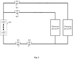
- Fig. 2 is a schematic structural diagram of a specific implementation of a charge and discharge circuit not covered by the present invention.
- the first switch set P4 includes a first switch K1, a second switch K2 and a third switch K3.
- the second switch set P5 includes the first switch K1, the second switch K2 and a fourth switch K4.
- a first end of the first switch K1 is connected to a negative electrode of the battery pack P1.
- a second end of the first switch K1 is connected to a second end of the second switch K2.
- a first end of the second switch K2 is connected to one end of the charging device P2.
- the other end of the charging device P2 is connected to a first end of the third switch K3, and a second end of the third switch K3 is connected to a positive electrode of the battery pack P1.
- the first end of the second switch K2 is connected to one end of the electrical device P3.
- the other end of the electrical device P3 is connected to a second end of the fourth switch K4.
- a first end of the fourth switch K4 is connected to the positive electrode of the battery pack P1.
- the first switch K1, the second switch K2, the third switch K3 and the fourth switch K4 are all semiconductor switches.
- positions of the first switch K1 and the second switch K2 in Fig. 2 may be exchanged, that is, the negative electrode of the battery pack P1 is connected to the second end of the second switch K2, the first end of the second switch K2 is connected to the first end of the first switch K1, and the second end of the first switch K1 is connected to one end of the charging device P2 and one end of the electrical device P3.
- the charge circuit includes three semiconductor switches connected in series
- the discharge circuit includes three semiconductor switches connected in series.
- the charge circuit and the discharge circuit share the first switch K1 and the second switch K2.
- the second end (i.e. a source) of the first switch K1 is connected to the second end (i.e. a source) of the second switch K2. It is ensured that the parasitic diodes of the first switch K1 and the second switch K2 will not turned on at the same time, thereby ensuring the realization of the switching function and avoiding the wrong turn-on of the charge circuit and the discharge circuit.
- the charge and discharge circuit may realize four processes of pre-charging of charging, charging, pre-charging of discharging and discharging of the battery pack P1.
- the controller may send control signals to the first switch K1, the second switch K2, the third switch K3 and the fourth switch K4. Specifically, the controller can send control signals to the control ends of the first switch K1, the second switch K2, the third switch K3 and the fourth switch K4, so as to realize the turn-on and turn-off of the first switch K1, the second switch K2, the third switch K3 and the fourth switch K4.
- the first switch K1 and the third switch K3 are turned on, the fourth switch K4 is turned off, and the second switch K2 is turned on at intervals, so as to realize the interval turn-on of the charge circuit to pre-charge the charging device P2.
- the controller may send a turn-on signal to the first switch K1 and the third switch K3 to control both the first switch K1 and the third switch K3 to be turned on.
- the controller sends a turn-off signal to the fourth switch K4 to control the fourth switch K4 to be turned off.
- the controller sends a pulse signal to the second switch K2 to control the second switch K2 to be turned on at intervals, so as to pre-charge the charging device P2.
- the first switch K1, the second switch K2 and the third switch K3 are turned on, and the fourth switch K4 is turned off.
- the controller may send a turn-on signal to the first switch K1 and the third switch K3 to control the first switch K1 and the third switch K3 to be turned on.
- the controller sends a turn-off signal to the fourth switch K4 to control the fourth switch K4 to be turned off, so as to allow the charging device P2 to charge the battery pack P1.
- the turn-on direction of the parasitic diode in the second switch K2 is from the second end to the first end. Therefore, whether the second switch K2 is turned on or turned off, the parasitic diode in the second switch K2 is turned on.
- a turn- on instruction may be sent to the second switch K2.
- the charging process may be triggered by the turn-on control of the first switch K1 and the third switch K3.
- the first switch K1 and the fourth switch K4 are turned on, the third switch K3 is turned off, and the second switch K2 is turned on at intervals.
- the controller sends a turn-on signal to the first switch K1 and the fourth switch K4 to control the first switch K1 and the fourth switch K4 to be turned on.
- the controller sends a turn-off signal to the third switch K3 to control the third switch K3 to be turned off.
- the controller sends a pulse signal to the second switch K2 to control the second switch K2 to be turned on at intervals, so as to pre-charge the electrical device P3.
- the first switch K1, the second switch K2 and the fourth switch K4 are turned on, and the third switch K3 is tuned off.
- the controller may send a turn-on signal to the first switch K1, the second switch K2 and the fourth switch K4 to control the first switch K1, the second switch K2 and the fourth switch K4 to be turned on.
- the controller sends a turn-off signal to the third switch K3 to control the third switch K3 to be turned off, so as to allow the battery pack P1 to discharge to the electrical device P3.
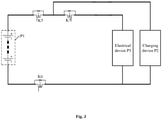
- Fig. 3 is a schematic structural diagram of another specific implementation of a charge and discharge circuit not covered by the present invention.
- the first switch set P4 includes a fifth switch K5 and a sixth switch K6.
- the second switch set P5 includes the fifth switch K5, the sixth switch K6 and a seventh switch K7.
- a second end of the fifth switch K5 is connected to a positive electrode of the battery pack P1.
- a first end of the fifth switch K5 is connected to one end of the charging device P2.
- the other end of the charging device P2 is connected to a first end of the sixth switch K6.
- a second end of the sixth switch K6 is connected to a negative electrode of the battery pack P1.
- the first end of the fifth switch K5 is connected to a first end of the seventh switch K7.
- a second end of the seventh switch K7 is connected to one end of the electrical device P3.
- the other end of the electrical device P3 is connected to the first end of the sixth switch K6.
- the fifth switch K5, the sixth switch K6 and the seventh switch K7 are all semiconductor switches.
- the charge circuit includes two semiconductor switches connected in series, and the discharge circuit includes three semiconductor switches connected in series.
- the charge circuit and the discharge circuit share the fifth switch K5 and the sixth switch K6.
- a smaller number of semiconductor switches are used, which reduces the total on-resistance of the semiconductor switches in the charge and discharge circuit, thereby reducing the total on-power consumption of the semiconductor switches in the charge and discharge circuit.
- the controller may send control signals to the fifth switch K5, the sixth switch K6 and the seventh switch K7. Specifically, the controller may send control signals to the control ends of the fifth switch K5, the sixth switch K6 and the seventh switch K7 to realize the turn-on and turn-off of the fifth switch K5, the sixth switch K6 and the seventh switch K7.
- the fifth switch K5 is turned on, the seventh switch K7 is turned off, and the sixth switch K6 is turned on at intervals, so as to realize the interval turn-on of the charge circuit to pre-charge the charging device P2.
- the controller sends a turn-on signal to the fifth switch K5 to control the fifth switch K5 to be turned on.
- the controller sends a turn-off signal to the seventh switch K7 to control the seventh switch K7 to be turned off.
- the controller sends a pulse signal to the sixth switch K6 to control the sixth switch K6 to be turned on at intervals, so as to pre-charge the charging device P2.
- the fifth switch K5 and the sixth switch K6 are turned on, and the seventh switch K7 is tuned off.
- the controller sends a turn-on signal to the fifth switch K5 and the sixth switch K6 to control the fifth switch K5 and the sixth switch K6 to be turned on.
- the controller sends a turn-off signal to the seventh switch K7 to control the seventh switch K7 to be turned off, so as to allow the charging device P2 to charge the battery pack P1.
- the charging process is triggered by the turning on the fifth switch K5.
- the fifth switch K5 and the seventh switch K7 are turned on, and the sixth switch K6 is turned on at intervals.
- the controller sends a turn-on signal to the fifth switch K5 and the seventh switch K7 to control the fifth switch K5 and the seventh switch K7 to be turned on.
- the controller sends a pulse signal to the sixth switch K6 to control the sixth switch K6 to be turned on at intervals, so as to pre-charge the electrical device P3.
- the sixth switch K6 and the seventh switch K7 are turned on, and the fifth switch K5 is turned off.
- the controller sends a turn-on signal the fifth switch K5, the sixth switch K6 and the seventh switch K7 to control the fifth switch K5, the sixth switch K6 and the seventh switch K7 to be turned on, so as to allow the battery pack P1 to discharge to the electrical device P3.
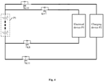
- Fig. 4 is a schematic structural diagram of yet another specific implementation of a charge and discharge circuit according to an embodiment of the present invention.
- the second switch set P5 includes an eighth switch K8 and a ninth switch K9.
- the first switch set P4 includes a tenth switch K10 and an eleventh switch K11.
- a second end of the eighth switch K8 is connected to the negative electrode of the battery pack P1, a first end of the eighth switch K8 is connected to one end of the electrical device P3, the other end of the electrical device P3 is connected to a second end of the ninth switch K9, and a first end of the ninth switch K9 is connected to the positive electrode of the battery pack P1.
- a second end of the tenth switch K10 is connected to the positive electrode of the battery pack P1, a first end of the tenth switch K10 is connected to the other end of the charging device P2, a second end of the eleventh switch K11 is connected to the negative electrode of the battery pack P1, and a first end of the eleventh switch K11 is connected to the one end of the charging device P2.
- the eighth switch K8, the ninth switch K9, the tenth switch K10 and the eleventh switch K11 are all semiconductor switches.
- the charge circuit includes two semiconductor switches connected in series
- the discharge circuit includes two semiconductor switches connected in series.
- the controller may send control signals to the eighth switch K8, the ninth switch K9, the tenth switch K10 and the eleventh switch K11. Specifically, the controller may send control signals to control ends of the eighth switch K8, the ninth switch K9, the tenth switch K10 and the eleventh switch K11 to realize the turn-on and turn-off of the eighth switch K8, the ninth switch K9, the tenth switch K10 and the eleventh switch K11.
- the tenth switch K10 is turned on, the eleventh switch K11 is turned on at intervals, and the eighth switch K8 and the ninth switch K9 are turned off.
- the controller sends a turn-on signal to the tenth switch K10 to control the tenth switch K10 to be turned on.
- the controller sends a turn-off signal to the eighth switch K8 and the ninth switch K9 to control the eighth switch K8 and the ninth switch K9 to be turned off.
- the controller sends a pulse signal to the eleventh switch K11 to control the eleventh switch K11 to be turned on at intervals, so as to pre-charge the charging device P2.
- the tenth switch K10 and the eleventh switch K11 are turned, and the eighth switch K8 and the ninth switch K9 are turned off.
- the controller sends a turn-on signal to the tenth switch K10 and the eleventh switch K11 to control the tenth switch K10 and the eleventh switch K11 to be turned on.
- the controller sends a turn-off signal to the eighth switch K8 and the ninth switch K9 to control the eighth switch K8 and the ninth switch K9 to be turned off, so as to allow the charging device P2 to charge the battery pack P1.
- the ninth switch K9 is turned on, the tenth switch K10 and the eleventh switch K11 are turned off, and the eighth switch K8 is turned on at intervals.
- the controller sends a turn-on signal to the ninth switch K9 to control the ninth switch K9 to be turned on.
- the controller sends a turn-off signal to the tenth switch K10 and the eleventh switch K11 to control the tenth switch K10 and the eleventh switch K11 to be turned off.
- the controller sends a pulse signal to the eighth switch K8 to control the eighth switch K8 to be turned on at intervals, so as to pre-charge the electrical device P3.
- the eighth switch K8 and the ninth switch K9 are turned on, and the tenth switch K10 and the eleventh switch K11 are turned off.
- the controller sends a turn-on signal to the eighth switch K8 and the ninth switch K9 to control the eighth switch K8 and the ninth switch K9 to be turned on.
- the controller sends a turn-off signal to the tenth switch K10 and the eleventh switch K11 to control the tenth switch K10 and the eleventh switch K11 to be turned off, so as to allow the battery pack P1 to discharge to the electrical device P3.
- pre-charging the charging device specifically refers to pre-charging a capacitor in the charging device.
- Pre-charging the electrical device specifically refers to pre-charging the capacitor in the electrical device.
Landscapes
- Engineering & Computer Science (AREA)
- Power Engineering (AREA)
- Charge And Discharge Circuits For Batteries Or The Like (AREA)
- Secondary Cells (AREA)
Description
- The present disclosure relates to field of battery power, and particularly to a charge and discharge circuit.
- With rapid development of new energy, new energy may provide power for more and more devices. For example, a battery module, a battery pack and the like may be used as a power source to provide power for new energy vehicles, new energy ships, new energy airplanes, etc. The battery module, battery pack and the like may be charged and discharged for many times during use.
- At present, a relay is disposed in the charge and discharge circuit. The charging and discharging of the battery module, the battery pack or the like in the charge and discharge circuit is controlled by controlling on and off of the relay. However, due to low switching speed and high failure rate of the relay, it adversely affects the charging and discharging of the battery module, the battery pack or the like, and reduces the charging and discharging capability of the charge and discharge circuit.
- D1 (
US 2007/0188140 A1 ) discloses a charging-discharging control device with low cost and high efficiency comprising all features in the preamble of claim 1. - The charging-discharging control device includes a selector having eight transistors. Every two transistors with different current directions are traditionally connected in series to form a switch. The switch can be completely turned off to isolate the influence between different charging-discharging paths. D2 (
US 2011/0084667 A1 ) discloses circuits and methods for controlling a current flowing through a battery. In particular, a trickle charging or discharging current through the battery is determined by a duty cycle of the PWM signal applied on a charge MOSFET or a discharge MOSFET, respectively, wherein said MOSFETs are connected in series with each other and with the battery. D3 (US 5 789 900 A ) discloses a device applicable to a power source unit removably mounted to a portable electronic apparatus. The device comprises two MOSFETs connected in series with each other and with the battery as well. Its teaching covers the possibility that one of said MOSFETs be connected to the positive terminal of the battery and the other MOSFET be connected to the negative terminal, thereby avoiding an occurrence that when the controller turns off one of the MOSFETs, the resulting extremely high momentary voltage is applied to the other MOSFET and renders the parasitic diode thereof conductive. D4 (US 2007/0075684 A1 ) discloses a battery charging and discharging circuit with low cost and high efficiency. - The invention is set out in the appended set of claims.
- The present disclosure may be better understood from the following description of the Detailed Description of the present disclosure with reference to the attached drawings, where the same or similar reference numbers represent the same or similar features.
-
Fig. 1 is a schematic structural diagram of a charge and discharge circuit according to an example not covered by the present invention; -
Fig. 2 is a schematic structural diagram of a specific implementation of a charge and discharge circuit according to an example not covered by the present invention; -
Fig. 3 is a schematic structural diagram of another specific implementation of a charge and discharge circuit according to an example not covered by the present invention; and -
Fig. 4 is a schematic structural diagram of yet another specific implementation of a charge and discharge circuit according to an embodiment of the present invention. - Various aspects of features, examples not covered by the invention (but useful for understanding it) and embodiments of the invention will be described in detail below. A number of specific details are presented in the following detailed description to provide a comprehensive understanding of the present disclosure. However, it will be apparent to those skilled in the art that the present disclosure may be practiced without some of these specific details. The following description is merely to provide a better understanding of the present disclosure by illustrating examples thereof. The present disclosure is by no means limited to any specific configuration and algorithm set forth below, but covers any modification, replacement and improvement of elements, components and algorithms without departing from the present disclosure. Well-known structures and techniques are not shown in the drawings and the following description, so as to avoid unnecessary ambiguity of the present disclosure.
- The present disclosure provides a charge and discharge circuit, which may be applied to a scenario in which a battery pack is charged and discharged. The battery pack includes at least one battery module or at least one battery unit, which is not limited herein.
- The battery pack may be applied to an electric vehicle to supply power for the electric motor as a power source of the electric vehicle. The battery pack may also supply power for other electrical devices in the electric vehicle, such as an in-car air conditioner, a vehicle player, etc.
-
Fig. 1 is a schematic structural diagram of a charge and discharge circuit according to an example not covered by the present invention. As shown inFig. 1 , the charge and discharge circuit includes a charge circuit and a discharge circuit. A battery pack P1 is charged by the charge circuit and discharged by the discharge circuit. Furthermore, the charge circuit of the present disclosure may also be used to pre-charge a charging device, and the discharge circuit may be used to pre-charge an electrical device. - The charge circuit includes a battery pack P1, a first switch set P4 and a charging device P2 connected in series. The first switch set P4 includes at least one switch. The distribution of the switches in the first switch set P4 is not limited. For example, if the first switch set P4 includes a plurality of switches, a part of the switches may be distributed between a positive electrode of the battery pack P1 and the charging device P2, and the other part of switches may be distributed between a negative electrode of the battery pack P1 and the charging device P2. The charging device P2 is a device for charging the battery pack P1. When the battery pack P1 is charged, the charge circuit is turned on.
- The discharge circuit includes the battery pack P1, a second switch set P5 and an electrical device P3 connected in series. The second switch set P5 includes at least one switch. The distribution of the switches in the second switch set P5 is not limited. For example, if the second switch set P5 includes a plurality of switches, a part of the switches may be distributed between the positive electrode of the battery pack P1 and the electrical device P3, and the other part of switches may be distributed between the negative electrode of the battery pack P1 and the electrical device P3. The electrical device P3 is a device that consumes the power discharged from the battery pack P1. When the battery module discharges the electrical device P3, the discharge circuit is turned on.
- It is worth mentioning that the first switch set P4 and the second switch set P5 may share one or more switches, which is not limited here. The specific content will be described in the following specific implementation.
- It should be noted that all switches in the first switch set P4 and the second switch set P5 are semiconductor switches. In some examples, the semiconductor switches may include a metal-oxide-semiconductor field-effect transistor (Metal-Oxide-Semiconductor Field-Effect Transistor, MOSFET) or an insulated gate bipolar transistor (Insulated Gate Bipolar Transistor, IGBT). Both MOSFET and IGBT may be cut off with load.
- It should be noted that the MOSFET has a gate, a source and a drain. There is a parasitic diode between the source and the drain of the MOSEFT, that is, there is a diode whose turn-on direction is from source to drain. The diode may be provided in the IGBT, whose turn-on direction is from source to drain. The diode may not be provided in the IGBT either, which is not limited herein.
- In some examples, if the MOSFET is used to perform a relay function, two MOSFETs with sources connected in series or two IGBTs with sources connected in series are required. That is to say, the first switch set P4 and/or the second switch set P5 at least includes two MOSFETs with sources connected in series or two IGBTs with sources connected in series. The two MOSFETs with sources connected in series or the two IGBTs with sources connected in series may be directly connected in series or indirectly connected in series, that is, the sources of the two MOSFETs or those of the two IGBTs may be connected in series by one or more devices, which is not limited herein.
- In some examples, the charge and discharge circuit further includes a controller which may be connected to various switches in the charge circuit and the discharge circuit. The controller may send a control signal to each switch in the charge circuit and the discharge circuit, so as to control turn-on or turn-off of each switch in the charge circuit and the discharge circuit. The control signal may include a turn-on signal, a turn-off signal, a pulse signal, etc., which is not limited herein. The pulse signal may specifically be a pulse width modulation (Pulse Width Modulation, PWM) signal.
- For example, the controller sends a turn-on signal to a part of switches in the first switch set P4 and sends a pulse signal to the other part of switches in the first switch set P4 to control the part of switches in the first switch set P4 to be turned on and the other part of switches to be turned on at intervals, so as to pre-charge the charging device P2.
- The controller may be configured to send a turn-on signal to the switches in the first switch set P4 to control the switches in the first switch set P4 to be turned on and realize the turn-on of the charge circuit, so as to allow the charging device P2 to charge the battery pack P1.
- The controller sends a turn-on signal to a part of switches in the second switch set P5 and sends a pulse signal to the other part of switches in the second switch set P5 to control the part of switches in the second switch set P5 to be turned on and the other part switches to be turned on at intervals, so as to pre-charge the electrical device P3.
- The controller sends a turn-on signal to the switches in the second switch set P5 to control the switches in the second switch set P5 to be turned on and realize the turn-on of the discharge circuit, so as to allow the battery pack P1 to discharge to the electrical device P3.
- It should be noted that other parts of the charging and discharging circuit other than the charging device P2 may be provided in an electric device or an electric system. For example, other parts of the charge and discharge circuit other than the charging device P2 may be provided in an electric vehicle, and the electrical device P3 is an electrical portion in the electric vehicle. The charging device P2 may specifically be a charging pile, a commercial power charging interface, or the like, which is not limited herein. The charging device P2 will only be connected to the charging circuit during the charging process. For example, the electric vehicle will be charged, and the electric vehicle will be connected to the charging pile. The charging device P2 itself may also be provided with a charging switch. When the charging device P2 is connected to the charging circuit and the charging switch is turned on, the charging device may then be conducted with other parts of the charge circuit.
- In the present disclosure, the charge and discharge circuit includes a battery pack P1, a charging device P2, an electrical device P3, a first switch set P4 and a second switch set P5. The battery pack P1, the first switch set P4 and the charging device P2 constitute a charge circuit, and the battery pack P1, the second switch set P5 and the electrical device P3 constitute a discharge circuit. All switches in the charge circuit and the discharge circuit are semiconductor switches. The semiconductor switches have smaller volume and weight, low failure rate and high switching speed, which can reduce adverse effect on the charging and discharging of the battery module, the battery pack and the like, and can improve the charging and discharging capability of the charge and discharge circuit. While the charging and discharging circuit is controlled safely, the switching devices in the charging and discharging circuit is prevented from being damaged. Furthermore, the overall volume and weight of the charge and discharge circuit using the semiconductor switch will also be reduced, and the probability of charging and discharging failure of the charge and discharge circuit is also decreased accordingly. The switching rate of the charge and discharge circuit according to the present disclosure is increased, and the controllability of the charging and discharging of the charge and discharge circuit is improved.
- Specific implementations of several charge and discharge circuits will be introduced in detail below. For ease of introduction, a semiconductor switch will be taken as an example, the semiconductor switch is a MOSFET, a first end of the MOSFET is a drain, a second end is a source, and a control end of the MOSFET is a gate. The diode between the drain and the source of the MOSFET is a parasitic diode.
-
Fig. 2 is a schematic structural diagram of a specific implementation of a charge and discharge circuit not covered by the present invention. - As shown in
Fig. 2 , the first switch set P4 includes a first switch K1, a second switch K2 and a third switch K3. The second switch set P5 includes the first switch K1, the second switch K2 and a fourth switch K4. - A first end of the first switch K1 is connected to a negative electrode of the battery pack P1. A second end of the first switch K1 is connected to a second end of the second switch K2. A first end of the second switch K2 is connected to one end of the charging device P2. The other end of the charging device P2 is connected to a first end of the third switch K3, and a second end of the third switch K3 is connected to a positive electrode of the battery pack P1.
- The first end of the second switch K2 is connected to one end of the electrical device P3. The other end of the electrical device P3 is connected to a second end of the fourth switch K4. A first end of the fourth switch K4 is connected to the positive electrode of the battery pack P1. The first switch K1, the second switch K2, the third switch K3 and the fourth switch K4 are all semiconductor switches.
- In some examples, positions of the first switch K1 and the second switch K2 in
Fig. 2 may be exchanged, that is, the negative electrode of the battery pack P1 is connected to the second end of the second switch K2, the first end of the second switch K2 is connected to the first end of the first switch K1, and the second end of the first switch K1 is connected to one end of the charging device P2 and one end of the electrical device P3. - As can be seen from
Fig. 2 , the charge circuit includes three semiconductor switches connected in series, and the discharge circuit includes three semiconductor switches connected in series. The charge circuit and the discharge circuit share the first switch K1 and the second switch K2. The second end (i.e. a source) of the first switch K1 is connected to the second end (i.e. a source) of the second switch K2. It is ensured that the parasitic diodes of the first switch K1 and the second switch K2 will not turned on at the same time, thereby ensuring the realization of the switching function and avoiding the wrong turn-on of the charge circuit and the discharge circuit. - The charge and discharge circuit may realize four processes of pre-charging of charging, charging, pre-charging of discharging and discharging of the battery pack P1.
- The controller may send control signals to the first switch K1, the second switch K2, the third switch K3 and the fourth switch K4. Specifically, the controller can send control signals to the control ends of the first switch K1, the second switch K2, the third switch K3 and the fourth switch K4, so as to realize the turn-on and turn-off of the first switch K1, the second switch K2, the third switch K3 and the fourth switch K4.
- During the pre-charging process of charging, the first switch K1 and the third switch K3 are turned on, the fourth switch K4 is turned off, and the second switch K2 is turned on at intervals, so as to realize the interval turn-on of the charge circuit to pre-charge the charging device P2.
- Specifically, the controller may send a turn-on signal to the first switch K1 and the third switch K3 to control both the first switch K1 and the third switch K3 to be turned on. The controller sends a turn-off signal to the fourth switch K4 to control the fourth switch K4 to be turned off. The controller sends a pulse signal to the second switch K2 to control the second switch K2 to be turned on at intervals, so as to pre-charge the charging device P2.
- During the charging process, the first switch K1, the second switch K2 and the third switch K3 are turned on, and the fourth switch K4 is turned off.
- Specifically, the controller may send a turn-on signal to the first switch K1 and the third switch K3 to control the first switch K1 and the third switch K3 to be turned on. The controller sends a turn-off signal to the fourth switch K4 to control the fourth switch K4 to be turned off, so as to allow the charging device P2 to charge the battery pack P1.
- It should be noted that the turn-on direction of the parasitic diode in the second switch K2 is from the second end to the first end. Therefore, whether the second switch K2 is turned on or turned off, the parasitic diode in the second switch K2 is turned on. A turn- on instruction may be sent to the second switch K2. The charging process may be triggered by the turn-on control of the first switch K1 and the third switch K3.
- In the pre-charging process of discharging, the first switch K1 and the fourth switch K4 are turned on, the third switch K3 is turned off, and the second switch K2 is turned on at intervals.
- Specifically, the controller sends a turn-on signal to the first switch K1 and the fourth switch K4 to control the first switch K1 and the fourth switch K4 to be turned on. The controller sends a turn-off signal to the third switch K3 to control the third switch K3 to be turned off. The controller sends a pulse signal to the second switch K2 to control the second switch K2 to be turned on at intervals, so as to pre-charge the electrical device P3.
- During the discharging process, the first switch K1, the second switch K2 and the fourth switch K4 are turned on, and the third switch K3 is tuned off.
- Specifically, the controller may send a turn-on signal to the first switch K1, the second switch K2 and the fourth switch K4 to control the first switch K1, the second switch K2 and the fourth switch K4 to be turned on. The controller sends a turn-off signal to the third switch K3 to control the third switch K3 to be turned off, so as to allow the battery pack P1 to discharge to the electrical device P3.
-
Fig. 3 is a schematic structural diagram of another specific implementation of a charge and discharge circuit not covered by the present invention. - As shown in
Fig. 3 , the first switch set P4 includes a fifth switch K5 and a sixth switch K6. The second switch set P5 includes the fifth switch K5, the sixth switch K6 and a seventh switch K7. - A second end of the fifth switch K5 is connected to a positive electrode of the battery pack P1. A first end of the fifth switch K5 is connected to one end of the charging device P2. The other end of the charging device P2 is connected to a first end of the sixth switch K6. A second end of the sixth switch K6 is connected to a negative electrode of the battery pack P1.
- The first end of the fifth switch K5 is connected to a first end of the seventh switch K7. A second end of the seventh switch K7 is connected to one end of the electrical device P3. The other end of the electrical device P3 is connected to the first end of the sixth switch K6.
- The fifth switch K5, the sixth switch K6 and the seventh switch K7 are all semiconductor switches.
- As can be seen from
Fig. 3 , the charge circuit includes two semiconductor switches connected in series, and the discharge circuit includes three semiconductor switches connected in series. The charge circuit and the discharge circuit share the fifth switch K5 and the sixth switch K6. There are a total of three semiconductor switches in the charge and discharge circuit. As compared withFig. 2 , a smaller number of semiconductor switches are used, which reduces the total on-resistance of the semiconductor switches in the charge and discharge circuit, thereby reducing the total on-power consumption of the semiconductor switches in the charge and discharge circuit. - The controller may send control signals to the fifth switch K5, the sixth switch K6 and the seventh switch K7. Specifically, the controller may send control signals to the control ends of the fifth switch K5, the sixth switch K6 and the seventh switch K7 to realize the turn-on and turn-off of the fifth switch K5, the sixth switch K6 and the seventh switch K7.
- During the pre-charging process of charging, the fifth switch K5 is turned on, the seventh switch K7 is turned off, and the sixth switch K6 is turned on at intervals, so as to realize the interval turn-on of the charge circuit to pre-charge the charging device P2.
- Specifically, the controller sends a turn-on signal to the fifth switch K5 to control the fifth switch K5 to be turned on. The controller sends a turn-off signal to the seventh switch K7 to control the seventh switch K7 to be turned off. The controller sends a pulse signal to the sixth switch K6 to control the sixth switch K6 to be turned on at intervals, so as to pre-charge the charging device P2.
- During the charging process, the fifth switch K5 and the sixth switch K6 are turned on, and the seventh switch K7 is tuned off.
- Specifically, the controller sends a turn-on signal to the fifth switch K5 and the sixth switch K6 to control the fifth switch K5 and the sixth switch K6 to be turned on. The controller sends a turn-off signal to the seventh switch K7 to control the seventh switch K7 to be turned off, so as to allow the charging device P2 to charge the battery pack P1.
- It should be noted that the charging process is triggered by the turning on the fifth switch K5. During the pre-charging process of discharging, the fifth switch K5 and the seventh switch K7 are turned on, and the sixth switch K6 is turned on at intervals.
- Specifically, the controller sends a turn-on signal to the fifth switch K5 and the seventh switch K7 to control the fifth switch K5 and the seventh switch K7 to be turned on. The controller sends a pulse signal to the sixth switch K6 to control the sixth switch K6 to be turned on at intervals, so as to pre-charge the electrical device P3.
- During the discharging process, the sixth switch K6 and the seventh switch K7 are turned on, and the fifth switch K5 is turned off.
- Specifically, the controller sends a turn-on signal the fifth switch K5, the sixth switch K6 and the seventh switch K7 to control the fifth switch K5, the sixth switch K6 and the seventh switch K7 to be turned on, so as to allow the battery pack P1 to discharge to the electrical device P3.
-
Fig. 4 is a schematic structural diagram of yet another specific implementation of a charge and discharge circuit according to an embodiment of the present invention. - As shown in
Fig. 4 , the second switch set P5 includes an eighth switch K8 and a ninth switch K9. The first switch set P4 includes a tenth switch K10 and an eleventh switch K11. - A second end of the eighth switch K8 is connected to the negative electrode of the battery pack P1, a first end of the eighth switch K8 is connected to one end of the electrical device P3, the other end of the electrical device P3 is connected to a second end of the ninth switch K9, and a first end of the ninth switch K9 is connected to the positive electrode of the battery pack P1.
- A second end of the tenth switch K10 is connected to the positive electrode of the battery pack P1, a first end of the tenth switch K10 is connected to the other end of the charging device P2, a second end of the eleventh switch K11 is connected to the negative electrode of the battery pack P1, and a first end of the eleventh switch K11 is connected to the one end of the charging device P2.
- The eighth switch K8, the ninth switch K9, the tenth switch K10 and the eleventh switch K11 are all semiconductor switches.
- As shown in
Fig. 4 , the charge circuit includes two semiconductor switches connected in series, and the discharge circuit includes two semiconductor switches connected in series. - The controller may send control signals to the eighth switch K8, the ninth switch K9, the tenth switch K10 and the eleventh switch K11. Specifically, the controller may send control signals to control ends of the eighth switch K8, the ninth switch K9, the tenth switch K10 and the eleventh switch K11 to realize the turn-on and turn-off of the eighth switch K8, the ninth switch K9, the tenth switch K10 and the eleventh switch K11.
- During the pre-charging process of charging, the tenth switch K10 is turned on, the eleventh switch K11 is turned on at intervals, and the eighth switch K8 and the ninth switch K9 are turned off.
- Specifically, the controller sends a turn-on signal to the tenth switch K10 to control the tenth switch K10 to be turned on. The controller sends a turn-off signal to the eighth switch K8 and the ninth switch K9 to control the eighth switch K8 and the ninth switch K9 to be turned off.
- The controller sends a pulse signal to the eleventh switch K11 to control the eleventh switch K11 to be turned on at intervals, so as to pre-charge the charging device P2.
- During the charging process, the tenth switch K10 and the eleventh switch K11 are turned, and the eighth switch K8 and the ninth switch K9 are turned off.
- Specifically, the controller sends a turn-on signal to the tenth switch K10 and the eleventh switch K11 to control the tenth switch K10 and the eleventh switch K11 to be turned on. The controller sends a turn-off signal to the eighth switch K8 and the ninth switch K9 to control the eighth switch K8 and the ninth switch K9 to be turned off, so as to allow the charging device P2 to charge the battery pack P1.
- During the pre-charging process of discharging, the ninth switch K9 is turned on, the tenth switch K10 and the eleventh switch K11 are turned off, and the eighth switch K8 is turned on at intervals.
- Specifically, the controller sends a turn-on signal to the ninth switch K9 to control the ninth switch K9 to be turned on. The controller sends a turn-off signal to the tenth switch K10 and the eleventh switch K11 to control the tenth switch K10 and the eleventh switch K11 to be turned off. The controller sends a pulse signal to the eighth switch K8 to control the eighth switch K8 to be turned on at intervals, so as to pre-charge the electrical device P3.
- During the discharging process, the eighth switch K8 and the ninth switch K9 are turned on, and the tenth switch K10 and the eleventh switch K11 are turned off.
- Specifically, the controller sends a turn-on signal to the eighth switch K8 and the ninth switch K9 to control the eighth switch K8 and the ninth switch K9 to be turned on. The controller sends a turn-off signal to the tenth switch K10 and the eleventh switch K11 to control the tenth switch K10 and the eleventh switch K11 to be turned off, so as to allow the battery pack P1 to discharge to the electrical device P3.
- It should be noted that in the foregoing description, pre-charging the charging device specifically refers to pre-charging a capacitor in the charging device. Pre-charging the electrical device specifically refers to pre-charging the capacitor in the electrical device.
- It should be clear that the disclosure in the present specification is presented in a progressive manner by focusing on the differences from other examples and embodiments. The present disclosure is not limited to the specific structures described above and illustrated in the drawings. A person skilled in the art may make various changes, modifications and additions after understanding the present disclosure.
- Those skilled in the art shall appreciate that the foregoing description is illustrative but not limiting.
- In the claims, the term "comprising" will not preclude another device(s) or step(s); the indefinite article "a/an" will not preclude plural; and the terms "first", "second", etc., are intended to designate a name but not to represent any specific order. Any reference number in the claims shall not be construed as limiting the scope of protection. Functions of a plurality of parts appearing in a claim may be performed by a separate hardware or software unit.
Claims (3)
- A charge and discharge circuit, comprising:a charge circuit comprising a battery pack (P1), a first switch set (P4) and a charging device (P2) connected in series, wherein the charge circuit is configured to charge the battery pack (P1) by using the charging device (P2) and pre-charge the charging device (P2); anda discharge circuit comprising the battery pack (P1), a second switch set (P5) and an electrical device (P3) connected in series, wherein the discharge circuit is configured to allow the battery pack (P1) to discharge to the electrical device (P3) and pre-charge the electrical device (P3);wherein both the first switch set (P4) and the second switch set (P5) include at least one switch, and all switches in the first switch set (P4) and the second switch set (P5) are semiconductor switches;wherein the second switch set (P5) comprises an eighth switch (K8) and a ninth switch (K9), the first switch set (P4) comprises a tenth switch (K10) and an eleventh switch (K11), a first end of the eighth switch (K8) is connected to one end of the electrical device (P3), and a first end of the tenth switch (K10) is connected to one end of the charging device (P2),the charge and discharge circuit is characterized in that:a second end of the eighth switch (K8) is connected to a negative electrode of the battery pack (P1), the other end of the electrical device (P3) is connected to a second end of the ninth switch (K9), and a first end of the ninth switch (K9) is connected to a positive electrode of the battery pack (P1);a second end of the tenth switch (K10) is connected to the positive electrode of the battery pack (P1), a second end of the eleventh switch (K11) is connected to the negative electrode of the battery pack (P1), and a first end of the eleventh switch (K11) is connected to the other end of the charging device (P2); andthe charge and discharge circuit further comprises a controller, and the controller is configured to:send a turn-on signal to the tenth switch (K10) to control the tenth switch (K10) to be turned on, send a turn-off signal to the eighth switch (K8) and the ninth switch (K9) to control the eighth switch (K8) and the ninth switch (K9) to be turned off, and send a pulse signal to the eleventh switch (K11) to control the eleventh switch (K11) to be turned on at intervals, so as to pre-charge the charging device (P2);send a turn-on signal to the tenth switch (K10) and the eleventh switch (K11) to control the tenth switch (K10) and the eleventh switch (K11) to be turned on, and send a turn-off signal to the eighth switch (K8) and the ninth switch (K9) to control the eighth switch (K8) and the ninth switch (K9) to be turned off, so as to allow the charging device (P2) to charge the battery pack (P1);send a turn-on signal to the ninth switch (K9) to control the ninth switch (K9) to be turned on, sending a turn-off signal to the tenth switch (K10) and the eleventh switch (K11) to control the tenth switch (K10) and the eleventh switch (K11) to be turned off, and send a pulse signal to the eighth switch (K8) to control the eighth switch (K8) to be turned on at intervals, so as to pre-charge the electrical device (P3); andsend a turn-on signal to the eighth switch (K8) and the ninth switch (K9) to control the eighth switch (K8) and the ninth switch (K9) to be turned on, and send turn-off signal to the tenth switch (K10) and the eleventh switch (K11) to control the tenth switch (K10) and the eleventh switch (K11) to be turned off, so as to allow the battery pack (P1) to discharge to the electrical device (P3).
- The charge and discharge circuit of claim 1, wherein the semiconductor switches include a MOSFET or an IGBT.
- The charge and discharge circuit of claim 2, wherein a first end of the MOSFET or the IGBT is a drain, and a second end of the MOSFET or the IGBT is a source.
Applications Claiming Priority (2)
| Application Number | Priority Date | Filing Date | Title |
|---|---|---|---|
| CN201811493731.9A CN110970962A (en) | 2018-12-07 | 2018-12-07 | Charging and discharging circuit |
| PCT/CN2019/123707 WO2020114497A1 (en) | 2018-12-07 | 2019-12-06 | Charging and discharging circuit |
Publications (3)
| Publication Number | Publication Date |
|---|---|
| EP3751696A1 EP3751696A1 (en) | 2020-12-16 |
| EP3751696A4 EP3751696A4 (en) | 2021-05-05 |
| EP3751696B1 true EP3751696B1 (en) | 2022-02-23 |
Family
ID=70029564
Family Applications (1)
| Application Number | Title | Priority Date | Filing Date |
|---|---|---|---|
| EP19893957.1A Active EP3751696B1 (en) | 2018-12-07 | 2019-12-06 | Charging and discharging circuit |
Country Status (4)
| Country | Link |
|---|---|
| US (1) | US11652352B2 (en) |
| EP (1) | EP3751696B1 (en) |
| CN (1) | CN110970962A (en) |
| WO (1) | WO2020114497A1 (en) |
Families Citing this family (1)
| Publication number | Priority date | Publication date | Assignee | Title |
|---|---|---|---|---|
| CN115459394A (en) * | 2022-09-25 | 2022-12-09 | 岱昆半导体(上海)有限公司 | Multi-battery management system with charging control function |
Family Cites Families (23)
| Publication number | Priority date | Publication date | Assignee | Title |
|---|---|---|---|---|
| US5789900A (en) * | 1994-12-05 | 1998-08-04 | Fuji Photo Film Co., Ltd. | Device for protecting a secondary battery from overcharge and overdischarge |
| US6118254A (en) * | 1999-07-30 | 2000-09-12 | Compaq Computer Corporation | Battery charge control architecture for constant voltage maximum power operation |
| CA2325595A1 (en) * | 2000-11-10 | 2002-05-10 | Jeffrey Phillips | Charger for a rechargeable nickel-zinc battery |
| US7642750B2 (en) | 2005-10-04 | 2010-01-05 | O2Micro International Limited | Battery charge/discharge control circuit |
| TWI307200B (en) * | 2006-02-16 | 2009-03-01 | Quanta Comp Inc | Controllable charging/discharging device |
| US7595609B2 (en) * | 2006-03-09 | 2009-09-29 | Dell Products L.P. | Battery system power path configuration and methods for implementing same |
| US8350529B2 (en) * | 2006-11-10 | 2013-01-08 | Lithium Balance A/S | Battery management system |
| JP5174421B2 (en) * | 2007-10-19 | 2013-04-03 | パナソニック株式会社 | Battery pack and battery system |
| US8154255B2 (en) * | 2009-01-30 | 2012-04-10 | Dell Products L.P. | Systems and methods for waking up a battery system |
| US8823323B2 (en) * | 2009-04-16 | 2014-09-02 | Valence Technology, Inc. | Batteries, battery systems, battery submodules, battery operational methods, battery system operational methods, battery charging methods, and battery system charging methods |
| US8143863B2 (en) | 2009-10-12 | 2012-03-27 | O2Micro, Inc | Circuits and methods for controlling a current flowing through a battery |
| US20110140673A1 (en) * | 2009-12-10 | 2011-06-16 | Texas Insturments Incorporated | Pulse width modulated battery charging |
| JP5544923B2 (en) * | 2010-02-24 | 2014-07-09 | セイコーエプソン株式会社 | Protection circuit and electronic equipment |
| CN103847531B (en) * | 2012-11-28 | 2016-06-08 | 北汽福田汽车股份有限公司 | A kind of electric automobile high-voltage electrical system and control method |
| WO2014141809A1 (en) * | 2013-03-13 | 2014-09-18 | Necエナジーデバイス株式会社 | Battery pack, mobile body, and control method |
| JP5652562B1 (en) * | 2013-09-19 | 2015-01-14 | 株式会社豊田自動織機 | MOSFET switch element abnormality diagnosis apparatus and method |
| EP3195445B1 (en) * | 2014-07-28 | 2020-12-02 | EC Power, LLC | Systems and methods for fast charging batteries at low temperatures |
| JP6569446B2 (en) * | 2015-10-07 | 2019-09-04 | 三菱自動車工業株式会社 | Battery control device |
| KR102519118B1 (en) * | 2016-02-24 | 2023-04-05 | 삼성에스디아이 주식회사 | Battery protection circuit |
| CN106206185A (en) | 2016-09-18 | 2016-12-07 | 天津十二策科技有限公司 | A kind of chopper with isolating device |
| KR102082380B1 (en) | 2016-11-02 | 2020-02-28 | 주식회사 엘지화학 | Method and system for controling driving current of load |
| CN206452129U (en) * | 2016-12-23 | 2017-08-29 | 深圳市超力源科技有限公司 | A kind of serondary lithium battery charging is unable to charge/discharge control circuit |
| CN108110868A (en) | 2018-02-14 | 2018-06-01 | 深圳市道通智能航空技术有限公司 | Battery cathode control loop protective device, battery component and unmanned plane |
-
2018
- 2018-12-07 CN CN201811493731.9A patent/CN110970962A/en active Pending
-
2019
- 2019-12-06 WO PCT/CN2019/123707 patent/WO2020114497A1/en not_active Ceased
- 2019-12-06 US US16/978,683 patent/US11652352B2/en active Active
- 2019-12-06 EP EP19893957.1A patent/EP3751696B1/en active Active
Also Published As
| Publication number | Publication date |
|---|---|
| CN110970962A (en) | 2020-04-07 |
| US20200403418A1 (en) | 2020-12-24 |
| EP3751696A4 (en) | 2021-05-05 |
| WO2020114497A1 (en) | 2020-06-11 |
| US11652352B2 (en) | 2023-05-16 |
| EP3751696A1 (en) | 2020-12-16 |
Similar Documents
| Publication | Publication Date | Title |
|---|---|---|
| US11418046B2 (en) | Charge and discharge circuit | |
| US20180019739A1 (en) | Switch drive circuit for switch reducing lc resonance | |
| US20220294340A1 (en) | Voltage regulation module, charging module, and charging pile | |
| US11303145B2 (en) | Charging system | |
| CN110073600A (en) | Semiconductor switch control device, power supply system | |
| US11728802B2 (en) | Drive circuit | |
| CN209159467U (en) | Control circuit and control system of battery pack main contactor | |
| US11600992B2 (en) | Electric protection circuit | |
| EP3751696B1 (en) | Charging and discharging circuit | |
| US12424856B2 (en) | Cell balancing apparatus, battery apparatus including the same, and cell balancing method | |
| US20190190390A1 (en) | Power electronic module for a charging station and corresponding charging station and electricity charging station | |
| US10468728B2 (en) | Electronic switching device of a battery management system, and battery | |
| US11831305B2 (en) | Circuit arrangement for switching switch elements | |
| CN116345591A (en) | Pre-charging devices, voltage converters and electric vehicles | |
| EP4454116A1 (en) | A safety power switching device, a voltage converter and an electrified vehicle | |
| US20230198519A1 (en) | Relay driving circuit and battery system having the same | |
| CN116022022B (en) | Charging devices and equipment for charging electric vehicles | |
| US20250340142A1 (en) | Power supply device, storage medium, and control method | |
| JP2012181925A (en) | Switching device | |
| CN110212739A (en) | Driving circuit for object switch | |
| JP2024020703A (en) | Power storage system, storage battery control device, and storage battery control method | |
| CN116488443A (en) | Discharge circuit of smoothing capacitor and power conversion circuit | |
| CN118971246A (en) | Control circuit and control method thereof, battery pack, and load switching circuit | |
| JP2005263479A (en) | Elevator equipment | |
| KR20190018593A (en) | Power converting apparatus |
Legal Events
| Date | Code | Title | Description |
|---|---|---|---|
| STAA | Information on the status of an ep patent application or granted ep patent |
Free format text: STATUS: THE INTERNATIONAL PUBLICATION HAS BEEN MADE |
|
| PUAI | Public reference made under article 153(3) epc to a published international application that has entered the european phase |
Free format text: ORIGINAL CODE: 0009012 |
|
| STAA | Information on the status of an ep patent application or granted ep patent |
Free format text: STATUS: REQUEST FOR EXAMINATION WAS MADE |
|
| 17P | Request for examination filed |
Effective date: 20200907 |
|
| AK | Designated contracting states |
Kind code of ref document: A1 Designated state(s): AL AT BE BG CH CY CZ DE DK EE ES FI FR GB GR HR HU IE IS IT LI LT LU LV MC MK MT NL NO PL PT RO RS SE SI SK SM TR |
|
| AX | Request for extension of the european patent |
Extension state: BA ME |
|
| A4 | Supplementary search report drawn up and despatched |
Effective date: 20210401 |
|
| RIC1 | Information provided on ipc code assigned before grant |
Ipc: H02J 7/00 20060101AFI20210326BHEP |
|
| GRAP | Despatch of communication of intention to grant a patent |
Free format text: ORIGINAL CODE: EPIDOSNIGR1 |
|
| STAA | Information on the status of an ep patent application or granted ep patent |
Free format text: STATUS: GRANT OF PATENT IS INTENDED |
|
| INTG | Intention to grant announced |
Effective date: 20211206 |
|
| GRAS | Grant fee paid |
Free format text: ORIGINAL CODE: EPIDOSNIGR3 |
|
| GRAA | (expected) grant |
Free format text: ORIGINAL CODE: 0009210 |
|
| STAA | Information on the status of an ep patent application or granted ep patent |
Free format text: STATUS: THE PATENT HAS BEEN GRANTED |
|
| DAV | Request for validation of the european patent (deleted) | ||
| DAX | Request for extension of the european patent (deleted) | ||
| RAP3 | Party data changed (applicant data changed or rights of an application transferred) |
Owner name: CONTEMPORARY AMPEREX TECHNOLOGY CO., LIMITED |
|
| AK | Designated contracting states |
Kind code of ref document: B1 Designated state(s): AL AT BE BG CH CY CZ DE DK EE ES FI FR GB GR HR HU IE IS IT LI LT LU LV MC MK MT NL NO PL PT RO RS SE SI SK SM TR |
|
| REG | Reference to a national code |
Ref country code: GB Ref legal event code: FG4D |
|
| REG | Reference to a national code |
Ref country code: CH Ref legal event code: EP |
|
| REG | Reference to a national code |
Ref country code: AT Ref legal event code: REF Ref document number: 1471188 Country of ref document: AT Kind code of ref document: T Effective date: 20220315 |
|
| REG | Reference to a national code |
Ref country code: IE Ref legal event code: FG4D |
|
| REG | Reference to a national code |
Ref country code: DE Ref legal event code: R096 Ref document number: 602019011971 Country of ref document: DE |
|
| REG | Reference to a national code |
Ref country code: LT Ref legal event code: MG9D |
|
| REG | Reference to a national code |
Ref country code: NL Ref legal event code: MP Effective date: 20220223 |
|
| REG | Reference to a national code |
Ref country code: AT Ref legal event code: MK05 Ref document number: 1471188 Country of ref document: AT Kind code of ref document: T Effective date: 20220223 |
|
| PG25 | Lapsed in a contracting state [announced via postgrant information from national office to epo] |
Ref country code: SE Free format text: LAPSE BECAUSE OF FAILURE TO SUBMIT A TRANSLATION OF THE DESCRIPTION OR TO PAY THE FEE WITHIN THE PRESCRIBED TIME-LIMIT Effective date: 20220223 Ref country code: RS Free format text: LAPSE BECAUSE OF FAILURE TO SUBMIT A TRANSLATION OF THE DESCRIPTION OR TO PAY THE FEE WITHIN THE PRESCRIBED TIME-LIMIT Effective date: 20220223 Ref country code: PT Free format text: LAPSE BECAUSE OF FAILURE TO SUBMIT A TRANSLATION OF THE DESCRIPTION OR TO PAY THE FEE WITHIN THE PRESCRIBED TIME-LIMIT Effective date: 20220623 Ref country code: NO Free format text: LAPSE BECAUSE OF FAILURE TO SUBMIT A TRANSLATION OF THE DESCRIPTION OR TO PAY THE FEE WITHIN THE PRESCRIBED TIME-LIMIT Effective date: 20220523 Ref country code: NL Free format text: LAPSE BECAUSE OF FAILURE TO SUBMIT A TRANSLATION OF THE DESCRIPTION OR TO PAY THE FEE WITHIN THE PRESCRIBED TIME-LIMIT Effective date: 20220223 Ref country code: LT Free format text: LAPSE BECAUSE OF FAILURE TO SUBMIT A TRANSLATION OF THE DESCRIPTION OR TO PAY THE FEE WITHIN THE PRESCRIBED TIME-LIMIT Effective date: 20220223 Ref country code: HR Free format text: LAPSE BECAUSE OF FAILURE TO SUBMIT A TRANSLATION OF THE DESCRIPTION OR TO PAY THE FEE WITHIN THE PRESCRIBED TIME-LIMIT Effective date: 20220223 Ref country code: ES Free format text: LAPSE BECAUSE OF FAILURE TO SUBMIT A TRANSLATION OF THE DESCRIPTION OR TO PAY THE FEE WITHIN THE PRESCRIBED TIME-LIMIT Effective date: 20220223 Ref country code: BG Free format text: LAPSE BECAUSE OF FAILURE TO SUBMIT A TRANSLATION OF THE DESCRIPTION OR TO PAY THE FEE WITHIN THE PRESCRIBED TIME-LIMIT Effective date: 20220523 |
|
| PG25 | Lapsed in a contracting state [announced via postgrant information from national office to epo] |
Ref country code: PL Free format text: LAPSE BECAUSE OF FAILURE TO SUBMIT A TRANSLATION OF THE DESCRIPTION OR TO PAY THE FEE WITHIN THE PRESCRIBED TIME-LIMIT Effective date: 20220223 Ref country code: LV Free format text: LAPSE BECAUSE OF FAILURE TO SUBMIT A TRANSLATION OF THE DESCRIPTION OR TO PAY THE FEE WITHIN THE PRESCRIBED TIME-LIMIT Effective date: 20220223 Ref country code: GR Free format text: LAPSE BECAUSE OF FAILURE TO SUBMIT A TRANSLATION OF THE DESCRIPTION OR TO PAY THE FEE WITHIN THE PRESCRIBED TIME-LIMIT Effective date: 20220524 Ref country code: FI Free format text: LAPSE BECAUSE OF FAILURE TO SUBMIT A TRANSLATION OF THE DESCRIPTION OR TO PAY THE FEE WITHIN THE PRESCRIBED TIME-LIMIT Effective date: 20220223 Ref country code: AT Free format text: LAPSE BECAUSE OF FAILURE TO SUBMIT A TRANSLATION OF THE DESCRIPTION OR TO PAY THE FEE WITHIN THE PRESCRIBED TIME-LIMIT Effective date: 20220223 |
|
| PG25 | Lapsed in a contracting state [announced via postgrant information from national office to epo] |
Ref country code: IS Free format text: LAPSE BECAUSE OF FAILURE TO SUBMIT A TRANSLATION OF THE DESCRIPTION OR TO PAY THE FEE WITHIN THE PRESCRIBED TIME-LIMIT Effective date: 20220623 |
|
| PG25 | Lapsed in a contracting state [announced via postgrant information from national office to epo] |
Ref country code: SM Free format text: LAPSE BECAUSE OF FAILURE TO SUBMIT A TRANSLATION OF THE DESCRIPTION OR TO PAY THE FEE WITHIN THE PRESCRIBED TIME-LIMIT Effective date: 20220223 Ref country code: SK Free format text: LAPSE BECAUSE OF FAILURE TO SUBMIT A TRANSLATION OF THE DESCRIPTION OR TO PAY THE FEE WITHIN THE PRESCRIBED TIME-LIMIT Effective date: 20220223 Ref country code: RO Free format text: LAPSE BECAUSE OF FAILURE TO SUBMIT A TRANSLATION OF THE DESCRIPTION OR TO PAY THE FEE WITHIN THE PRESCRIBED TIME-LIMIT Effective date: 20220223 Ref country code: EE Free format text: LAPSE BECAUSE OF FAILURE TO SUBMIT A TRANSLATION OF THE DESCRIPTION OR TO PAY THE FEE WITHIN THE PRESCRIBED TIME-LIMIT Effective date: 20220223 Ref country code: DK Free format text: LAPSE BECAUSE OF FAILURE TO SUBMIT A TRANSLATION OF THE DESCRIPTION OR TO PAY THE FEE WITHIN THE PRESCRIBED TIME-LIMIT Effective date: 20220223 Ref country code: CZ Free format text: LAPSE BECAUSE OF FAILURE TO SUBMIT A TRANSLATION OF THE DESCRIPTION OR TO PAY THE FEE WITHIN THE PRESCRIBED TIME-LIMIT Effective date: 20220223 |
|
| REG | Reference to a national code |
Ref country code: DE Ref legal event code: R097 Ref document number: 602019011971 Country of ref document: DE |
|
| PG25 | Lapsed in a contracting state [announced via postgrant information from national office to epo] |
Ref country code: AL Free format text: LAPSE BECAUSE OF FAILURE TO SUBMIT A TRANSLATION OF THE DESCRIPTION OR TO PAY THE FEE WITHIN THE PRESCRIBED TIME-LIMIT Effective date: 20220223 |
|
| PLBE | No opposition filed within time limit |
Free format text: ORIGINAL CODE: 0009261 |
|
| STAA | Information on the status of an ep patent application or granted ep patent |
Free format text: STATUS: NO OPPOSITION FILED WITHIN TIME LIMIT |
|
| 26N | No opposition filed |
Effective date: 20221124 |
|
| PG25 | Lapsed in a contracting state [announced via postgrant information from national office to epo] |
Ref country code: SI Free format text: LAPSE BECAUSE OF FAILURE TO SUBMIT A TRANSLATION OF THE DESCRIPTION OR TO PAY THE FEE WITHIN THE PRESCRIBED TIME-LIMIT Effective date: 20220223 |
|
| P01 | Opt-out of the competence of the unified patent court (upc) registered |
Effective date: 20230516 |
|
| PG25 | Lapsed in a contracting state [announced via postgrant information from national office to epo] |
Ref country code: IT Free format text: LAPSE BECAUSE OF FAILURE TO SUBMIT A TRANSLATION OF THE DESCRIPTION OR TO PAY THE FEE WITHIN THE PRESCRIBED TIME-LIMIT Effective date: 20220223 |
|
| REG | Reference to a national code |
Ref country code: CH Ref legal event code: PL |
|
| REG | Reference to a national code |
Ref country code: BE Ref legal event code: MM Effective date: 20221231 |
|
| PG25 | Lapsed in a contracting state [announced via postgrant information from national office to epo] |
Ref country code: LU Free format text: LAPSE BECAUSE OF NON-PAYMENT OF DUE FEES Effective date: 20221206 |
|
| PG25 | Lapsed in a contracting state [announced via postgrant information from national office to epo] |
Ref country code: LI Free format text: LAPSE BECAUSE OF NON-PAYMENT OF DUE FEES Effective date: 20221231 Ref country code: IE Free format text: LAPSE BECAUSE OF NON-PAYMENT OF DUE FEES Effective date: 20221206 Ref country code: CH Free format text: LAPSE BECAUSE OF NON-PAYMENT OF DUE FEES Effective date: 20221231 |
|
| PG25 | Lapsed in a contracting state [announced via postgrant information from national office to epo] |
Ref country code: BE Free format text: LAPSE BECAUSE OF NON-PAYMENT OF DUE FEES Effective date: 20221231 |
|
| PG25 | Lapsed in a contracting state [announced via postgrant information from national office to epo] |
Ref country code: CY Free format text: LAPSE BECAUSE OF FAILURE TO SUBMIT A TRANSLATION OF THE DESCRIPTION OR TO PAY THE FEE WITHIN THE PRESCRIBED TIME-LIMIT Effective date: 20220223 |
|
| PG25 | Lapsed in a contracting state [announced via postgrant information from national office to epo] |
Ref country code: MK Free format text: LAPSE BECAUSE OF FAILURE TO SUBMIT A TRANSLATION OF THE DESCRIPTION OR TO PAY THE FEE WITHIN THE PRESCRIBED TIME-LIMIT Effective date: 20220223 Ref country code: HU Free format text: LAPSE BECAUSE OF FAILURE TO SUBMIT A TRANSLATION OF THE DESCRIPTION OR TO PAY THE FEE WITHIN THE PRESCRIBED TIME-LIMIT; INVALID AB INITIO Effective date: 20191206 |
|
| PG25 | Lapsed in a contracting state [announced via postgrant information from national office to epo] |
Ref country code: MC Free format text: LAPSE BECAUSE OF FAILURE TO SUBMIT A TRANSLATION OF THE DESCRIPTION OR TO PAY THE FEE WITHIN THE PRESCRIBED TIME-LIMIT Effective date: 20220223 |
|
| PG25 | Lapsed in a contracting state [announced via postgrant information from national office to epo] |
Ref country code: MC Free format text: LAPSE BECAUSE OF FAILURE TO SUBMIT A TRANSLATION OF THE DESCRIPTION OR TO PAY THE FEE WITHIN THE PRESCRIBED TIME-LIMIT Effective date: 20220223 |
|
| REG | Reference to a national code |
Ref country code: DE Ref legal event code: R081 Ref document number: 602019011971 Country of ref document: DE Owner name: CONTEMPORARY AMPEREX TECHNOLOGY (HONG KONG) LI, HK Free format text: FORMER OWNER: CONTEMPORARY AMPEREX TECHNOLOGY CO., LIMITED, NINGDE CITY, FUJIAN, CN |
|
| REG | Reference to a national code |
Ref country code: GB Ref legal event code: 732E Free format text: REGISTERED BETWEEN 20240829 AND 20240904 |
|
| PG25 | Lapsed in a contracting state [announced via postgrant information from national office to epo] |
Ref country code: MT Free format text: LAPSE BECAUSE OF FAILURE TO SUBMIT A TRANSLATION OF THE DESCRIPTION OR TO PAY THE FEE WITHIN THE PRESCRIBED TIME-LIMIT Effective date: 20220223 |
|
| PGFP | Annual fee paid to national office [announced via postgrant information from national office to epo] |
Ref country code: FR Payment date: 20250930 Year of fee payment: 7 |
|
| PG25 | Lapsed in a contracting state [announced via postgrant information from national office to epo] |
Ref country code: TR Free format text: LAPSE BECAUSE OF FAILURE TO SUBMIT A TRANSLATION OF THE DESCRIPTION OR TO PAY THE FEE WITHIN THE PRESCRIBED TIME-LIMIT Effective date: 20220223 |
|
| PGFP | Annual fee paid to national office [announced via postgrant information from national office to epo] |
Ref country code: DE Payment date: 20250930 Year of fee payment: 7 |
|
| PGFP | Annual fee paid to national office [announced via postgrant information from national office to epo] |
Ref country code: GB Payment date: 20251001 Year of fee payment: 7 |