EP3751571A1 - Memory arrays with bonded and shared logic circuitry - Google Patents
Memory arrays with bonded and shared logic circuitry Download PDFInfo
- Publication number
- EP3751571A1 EP3751571A1 EP20162733.8A EP20162733A EP3751571A1 EP 3751571 A1 EP3751571 A1 EP 3751571A1 EP 20162733 A EP20162733 A EP 20162733A EP 3751571 A1 EP3751571 A1 EP 3751571A1
- Authority
- EP
- European Patent Office
- Prior art keywords
- logic circuitry
- layer
- memory
- array
- memory array
- Prior art date
- Legal status (The legal status is an assumption and is not a legal conclusion. Google has not performed a legal analysis and makes no representation as to the accuracy of the status listed.)
- Pending
Links
Images





Classifications
-
- G—PHYSICS
- G11—INFORMATION STORAGE
- G11C—STATIC STORES
- G11C5/00—Details of stores covered by group G11C11/00
- G11C5/02—Disposition of storage elements, e.g. in the form of a matrix array
- G11C5/025—Geometric lay-out considerations of storage- and peripheral-blocks in a semiconductor storage device
-
- H—ELECTRICITY
- H10—SEMICONDUCTOR DEVICES; ELECTRIC SOLID-STATE DEVICES NOT OTHERWISE PROVIDED FOR
- H10W—GENERIC PACKAGES, INTERCONNECTIONS, CONNECTORS OR OTHER CONSTRUCTIONAL DETAILS OF DEVICES COVERED BY CLASS H10
- H10W90/00—Package configurations
-
- H—ELECTRICITY
- H10—SEMICONDUCTOR DEVICES; ELECTRIC SOLID-STATE DEVICES NOT OTHERWISE PROVIDED FOR
- H10B—ELECTRONIC MEMORY DEVICES
- H10B41/00—Electrically erasable-and-programmable ROM [EEPROM] devices comprising floating gates
- H10B41/40—Electrically erasable-and-programmable ROM [EEPROM] devices comprising floating gates characterised by the peripheral circuit region
-
- G—PHYSICS
- G11—INFORMATION STORAGE
- G11C—STATIC STORES
- G11C5/00—Details of stores covered by group G11C11/00
- G11C5/02—Disposition of storage elements, e.g. in the form of a matrix array
- G11C5/04—Supports for storage elements, e.g. memory modules; Mounting or fixing of storage elements on such supports
-
- G—PHYSICS
- G11—INFORMATION STORAGE
- G11C—STATIC STORES
- G11C5/00—Details of stores covered by group G11C11/00
- G11C5/06—Arrangements for interconnecting storage elements electrically, e.g. by wiring
-
- G—PHYSICS
- G11—INFORMATION STORAGE
- G11C—STATIC STORES
- G11C5/00—Details of stores covered by group G11C11/00
- G11C5/12—Apparatus or processes for interconnecting storage elements, e.g. for threading magnetic cores
-
- H—ELECTRICITY
- H10—SEMICONDUCTOR DEVICES; ELECTRIC SOLID-STATE DEVICES NOT OTHERWISE PROVIDED FOR
- H10B—ELECTRONIC MEMORY DEVICES
- H10B41/00—Electrically erasable-and-programmable ROM [EEPROM] devices comprising floating gates
- H10B41/20—Electrically erasable-and-programmable ROM [EEPROM] devices comprising floating gates characterised by three-dimensional [3D] arrangements, e.g. with cells on different height levels
- H10B41/23—Electrically erasable-and-programmable ROM [EEPROM] devices comprising floating gates characterised by three-dimensional [3D] arrangements, e.g. with cells on different height levels with source and drain on different levels, e.g. with sloping channels
- H10B41/27—Electrically erasable-and-programmable ROM [EEPROM] devices comprising floating gates characterised by three-dimensional [3D] arrangements, e.g. with cells on different height levels with source and drain on different levels, e.g. with sloping channels the channels comprising vertical portions, e.g. U-shaped channels
-
- H—ELECTRICITY
- H10—SEMICONDUCTOR DEVICES; ELECTRIC SOLID-STATE DEVICES NOT OTHERWISE PROVIDED FOR
- H10B—ELECTRONIC MEMORY DEVICES
- H10B41/00—Electrically erasable-and-programmable ROM [EEPROM] devices comprising floating gates
- H10B41/50—Electrically erasable-and-programmable ROM [EEPROM] devices comprising floating gates characterised by the boundary region between the core region and the peripheral circuit region
-
- H—ELECTRICITY
- H10—SEMICONDUCTOR DEVICES; ELECTRIC SOLID-STATE DEVICES NOT OTHERWISE PROVIDED FOR
- H10B—ELECTRONIC MEMORY DEVICES
- H10B43/00—EEPROM devices comprising charge-trapping gate insulators
- H10B43/20—EEPROM devices comprising charge-trapping gate insulators characterised by three-dimensional [3D] arrangements, e.g. with cells on different height levels
- H10B43/23—EEPROM devices comprising charge-trapping gate insulators characterised by three-dimensional [3D] arrangements, e.g. with cells on different height levels with source and drain on different levels, e.g. with sloping channels
- H10B43/27—EEPROM devices comprising charge-trapping gate insulators characterised by three-dimensional [3D] arrangements, e.g. with cells on different height levels with source and drain on different levels, e.g. with sloping channels the channels comprising vertical portions, e.g. U-shaped channels
-
- H—ELECTRICITY
- H10—SEMICONDUCTOR DEVICES; ELECTRIC SOLID-STATE DEVICES NOT OTHERWISE PROVIDED FOR
- H10B—ELECTRONIC MEMORY DEVICES
- H10B43/00—EEPROM devices comprising charge-trapping gate insulators
- H10B43/40—EEPROM devices comprising charge-trapping gate insulators characterised by the peripheral circuit region
-
- H—ELECTRICITY
- H10—SEMICONDUCTOR DEVICES; ELECTRIC SOLID-STATE DEVICES NOT OTHERWISE PROVIDED FOR
- H10B—ELECTRONIC MEMORY DEVICES
- H10B43/00—EEPROM devices comprising charge-trapping gate insulators
- H10B43/50—EEPROM devices comprising charge-trapping gate insulators characterised by the boundary region between the core and peripheral circuit regions
-
- H—ELECTRICITY
- H10—SEMICONDUCTOR DEVICES; ELECTRIC SOLID-STATE DEVICES NOT OTHERWISE PROVIDED FOR
- H10W—GENERIC PACKAGES, INTERCONNECTIONS, CONNECTORS OR OTHER CONSTRUCTIONAL DETAILS OF DEVICES COVERED BY CLASS H10
- H10W20/00—Interconnections in chips, wafers or substrates
- H10W20/01—Manufacture or treatment
- H10W20/031—Manufacture or treatment of conductive parts of the interconnections
- H10W20/056—Manufacture or treatment of conductive parts of the interconnections by filling conductive material into holes, grooves or trenches
-
- H—ELECTRICITY
- H10—SEMICONDUCTOR DEVICES; ELECTRIC SOLID-STATE DEVICES NOT OTHERWISE PROVIDED FOR
- H10W—GENERIC PACKAGES, INTERCONNECTIONS, CONNECTORS OR OTHER CONSTRUCTIONAL DETAILS OF DEVICES COVERED BY CLASS H10
- H10W20/00—Interconnections in chips, wafers or substrates
- H10W20/01—Manufacture or treatment
- H10W20/071—Manufacture or treatment of dielectric parts thereof
- H10W20/081—Manufacture or treatment of dielectric parts thereof by forming openings in the dielectric parts
-
- H—ELECTRICITY
- H10—SEMICONDUCTOR DEVICES; ELECTRIC SOLID-STATE DEVICES NOT OTHERWISE PROVIDED FOR
- H10W—GENERIC PACKAGES, INTERCONNECTIONS, CONNECTORS OR OTHER CONSTRUCTIONAL DETAILS OF DEVICES COVERED BY CLASS H10
- H10W72/00—Interconnections or connectors in packages
- H10W72/071—Connecting or disconnecting
- H10W72/073—Connecting or disconnecting of die-attach connectors
-
- G—PHYSICS
- G11—INFORMATION STORAGE
- G11C—STATIC STORES
- G11C16/00—Erasable programmable read-only memories
- G11C16/02—Erasable programmable read-only memories electrically programmable
- G11C16/04—Erasable programmable read-only memories electrically programmable using variable threshold transistors, e.g. FAMOS
- G11C16/0483—Erasable programmable read-only memories electrically programmable using variable threshold transistors, e.g. FAMOS comprising cells having several storage transistors connected in series
-
- H—ELECTRICITY
- H10—SEMICONDUCTOR DEVICES; ELECTRIC SOLID-STATE DEVICES NOT OTHERWISE PROVIDED FOR
- H10W—GENERIC PACKAGES, INTERCONNECTIONS, CONNECTORS OR OTHER CONSTRUCTIONAL DETAILS OF DEVICES COVERED BY CLASS H10
- H10W72/00—Interconnections or connectors in packages
- H10W72/071—Connecting or disconnecting
- H10W72/073—Connecting or disconnecting of die-attach connectors
- H10W72/07331—Connecting techniques
-
- H—ELECTRICITY
- H10—SEMICONDUCTOR DEVICES; ELECTRIC SOLID-STATE DEVICES NOT OTHERWISE PROVIDED FOR
- H10W—GENERIC PACKAGES, INTERCONNECTIONS, CONNECTORS OR OTHER CONSTRUCTIONAL DETAILS OF DEVICES COVERED BY CLASS H10
- H10W72/00—Interconnections or connectors in packages
- H10W72/071—Connecting or disconnecting
- H10W72/073—Connecting or disconnecting of die-attach connectors
- H10W72/07351—Connecting or disconnecting of die-attach connectors characterised by changes in properties of the die-attach connectors during connecting
- H10W72/07354—Connecting or disconnecting of die-attach connectors characterised by changes in properties of the die-attach connectors during connecting changes in dispositions
-
- H—ELECTRICITY
- H10—SEMICONDUCTOR DEVICES; ELECTRIC SOLID-STATE DEVICES NOT OTHERWISE PROVIDED FOR
- H10W—GENERIC PACKAGES, INTERCONNECTIONS, CONNECTORS OR OTHER CONSTRUCTIONAL DETAILS OF DEVICES COVERED BY CLASS H10
- H10W72/00—Interconnections or connectors in packages
- H10W72/30—Die-attach connectors
- H10W72/341—Dispositions of die-attach connectors, e.g. layouts
- H10W72/347—Dispositions of multiple die-attach connectors
-
- H—ELECTRICITY
- H10—SEMICONDUCTOR DEVICES; ELECTRIC SOLID-STATE DEVICES NOT OTHERWISE PROVIDED FOR
- H10W—GENERIC PACKAGES, INTERCONNECTIONS, CONNECTORS OR OTHER CONSTRUCTIONAL DETAILS OF DEVICES COVERED BY CLASS H10
- H10W72/00—Interconnections or connectors in packages
- H10W72/30—Die-attach connectors
- H10W72/351—Materials of die-attach connectors
- H10W72/353—Materials of die-attach connectors not comprising solid metals or solid metalloids, e.g. ceramics
-
- H—ELECTRICITY
- H10—SEMICONDUCTOR DEVICES; ELECTRIC SOLID-STATE DEVICES NOT OTHERWISE PROVIDED FOR
- H10W—GENERIC PACKAGES, INTERCONNECTIONS, CONNECTORS OR OTHER CONSTRUCTIONAL DETAILS OF DEVICES COVERED BY CLASS H10
- H10W90/00—Package configurations
- H10W90/20—Configurations of stacked chips
- H10W90/22—Configurations of stacked chips the stacked chips being on both top and bottom sides of a package substrate, interposer or RDL
-
- H—ELECTRICITY
- H10—SEMICONDUCTOR DEVICES; ELECTRIC SOLID-STATE DEVICES NOT OTHERWISE PROVIDED FOR
- H10W—GENERIC PACKAGES, INTERCONNECTIONS, CONNECTORS OR OTHER CONSTRUCTIONAL DETAILS OF DEVICES COVERED BY CLASS H10
- H10W90/00—Package configurations
- H10W90/701—Package configurations characterised by the relative positions of pads or connectors relative to package parts
- H10W90/731—Package configurations characterised by the relative positions of pads or connectors relative to package parts of die-attach connectors
- H10W90/732—Package configurations characterised by the relative positions of pads or connectors relative to package parts of die-attach connectors between stacked chips
Definitions
- Flash memory such as NAND flash memory
- a flash memory array generally is coupled to logic circuits that facilitate operations of the memory array.
- the logic circuits have components such as word line drivers, bit line drivers, and sense amplifiers for the memory array.
- the logic circuits for example, include complementary metal-oxide-semiconductor (CMOS) logic.
- CMOS complementary metal-oxide-semiconductor
- thermal cycles of the process for formation of the memory array adversely affect the logic circuits.
- cost e.g., cost per bit of memory
- An integrated memory structure is disclosed herein, which includes multiple memory arrays, such as flash memory arrays, sharing a common logic circuitry.
- the shared logic circuitry is interposed between a first memory array and a second memory array.
- the first memory array and the second memory array are processed and formed separately from the logic circuitry. Subsequent to formation of the memory arrays and the logic circuitry, the logic circuitry is bonded to the first memory array and the second memory array.
- the integrated memory structure includes a first die comprising the first memory array, a second die comprising the second memory array, and a third die comprising the logic circuitry, where the third die is between the first and second dies, and the third die is bonded to each of the first and second dies.
- a first layer is deposited on a surface of the logic circuitry that is to be bonded with the memory array
- a second layer is deposited on a surface of the memory array that is to be bonded with the logic circuitry.
- Each of the first and second layer comprises, for example, an oxide material (such as silicon dioxide), a nitride material (such as silicon nitride), an oxynitride material (such as silicon oxynitride), and/or the like.
- the first and second layers are cleaned and polished, pre-bonded with one another, and annealed at an elevated temperature, thereby bonding the first and second layers to form a bonding interface layer.
- the logic circuit and the memory array are separated by the bonding interface layer.
- the bonding interface layer comprises silicon dioxide, silicon nitride, silicon oxynitride, or other suitable electrically-insulating bonding material.
- the thickness of the bonding interface layer can vary, in some embodiments it has a thickness in the range of 3000 angstroms to 10 microns.
- the bonding between the logic circuitry and a memory array may be formed using fusion bonding or hybrid bonding.
- the bonding process is between the first and second layers (and not between any conductive material such as metal).
- no conductive structure e.g., vias including metal
- via holes are formed extending through the bonding interface layer and are filled with metal, thereby forming interconnect structures between the logic circuitry and the memory array through the bonding interface layer.
- the bonding process is between the first and second layers and also between conductive structures within the first layer and conductive structures within the second layer.
- conductive structure e.g., a via including metal
- a first interconnect structure extends through the first layer and is exposed through, and flush with, a surface of the first layer; and a second interconnect structure extends through the second layer and is exposed through, and flush with, a surface of the second layer (e.g., prior to the bonding process).
- surfaces of the first layer and the second layers bond to form a bonding interface layer, along with a bonding or contact of the first interconnect structure and the second interconnect structure.
- the memory array and the logic circuitry may not be perfectly aligned during the bonding process, and hence, the first interconnect structure and the second interconnect structure may not be perfectly aligned while being bonded. Accordingly, sections of a combined interconnect structure formed through the bonding or contact of the first and second interconnect structures, which extend through the bonding interface layer, may have some misalignment or offset, as will be discussed in further detail in turn.
- Bonding the logic circuitry with two memory arrays and sharing the logic circuitry among the two memory arrays have several advantages. For example, sharing the logic circuitry among the memory arrays reduces complexity and/or power consumption of the logic circuitry. For example, a single shared voltage divider block of the logic circuitry can be used for both the memory arrays. Sharing the logic circuitry among the memory arrays also reduces cost of the logic circuitry per bit of memory. Thus, the cost of the logic circuitry is amortized across two memory arrays, thereby resulting in cost savings. Also, due to the use of the bonding process between the logic circuitry and the memory arrays, it is possible to separate the logic circuitry processing from the memory array processing, so that the logic circuitry is not affected by the thermal cycles of the process of memory array formation. Also, forming the memory arrays and the logic circuitry independently and separately reduces overall cycle time to manufacture the integrated memory structure.
- the logic circuitry can be bonded with a single memory array.
- the memory array and the logic circuitry are formed separately and then bonded (e.g., using fusion bonding or hybrid bonding).
- formation of the logic circuitry is separate from formation of the memory array, so that the logic circuitry is not affected by thermal cycles of the process of memory array formation.
- the logic circuitry is formed to be integrated with a first memory array (e.g., instead of bonding separately formed logic circuitry and the first memory array, a combined structure is formed that includes both the logic circuitry and the first memory array). After the combination of the first memory array and the logic circuitry is formed, the combination is then bonded with a second memory array. In the final memory structure, the logic circuitry is interposed between the first and second memory arrays. A bonding interface layer is between the logic circuitry and the second memory array (in other words, the combination of the first memory array and the logic circuitry is bonded with the second memory array). However, no such bonding interface layer is present between the logic circuitry and the first memory array. This alternate forming process still allows the logic circuitry to be shared among the first and second memory arrays, thereby reducing complexity, power consumption, and/or a cost per bit of the logic circuitry, as previously discussed herein.
- compositionally different refers to two materials that have different chemical compositions. This compositional difference may be, for instance, by virtue of an element that is in one material but not the other (e.g., SiGe is compositionally different than silicon), or by way of one material having all the same elements as a second material but at least one of those elements is intentionally provided at a different concentration in one material relative to the other material (e.g., SiGe having 70 atomic percent germanium is compositionally different than from SiGe having 25 atomic percent germanium).
- the materials may also have distinct dopants (e.g., gallium and magnesium) or the same dopants but at differing concentrations.
- compositionally distinct materials may further refer to two materials that have different crystallographic orientations. For instance, (110) silicon is compositionally distinct or different from (100) silicon. Creating a stack of different orientations could be accomplished, for instance, with blanket wafer layer transfer.
- the expression "X includes at least one of A or B” refers to an X that may include, for example, just A only, just B only, or both A and B. To this end, an X that includes at least one of A or B is not to be understood as an X that requires each of A and B, unless expressly so stated. For instance, the expression “X includes A and B” refers to an X that expressly includes both A and B. Moreover, this is true for any number of items greater than two, where "at least one of' those items are included in X.
- the expression "X includes at least one of A, B, or C” refers to an X that may include just A only, just B only, just C only, only A and B (and not C), only A and C (and not B), only B and C (and not A), or each of A, B, and C. This is true even if any of A, B, or C happens to include multiple types or variations. To this end, an X that includes at least one of A, B, or C is not to be understood as an X that requires each of A, B, and C, unless expressly so stated. For instance, the expression "X includes A, B, and C” refers to an X that expressly includes each of A, B, and C.
- X included in at least one of A or B refers to an X that may be included, for example, in just A only, in just B only, or in both A and B.
- X includes at least one of A or B” equally applies here, as will be appreciated.
- memory arrays 104a, 104b may be collectively and generally referred to as memory arrays 104 in plural, and memory array 104 in singular.
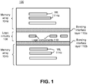
- Fig. 1 illustrates a cross-sectional view of an integrated memory structure 100 (also referred to as a structure 100) comprising a first memory array (also referred to as an "array") 104a, a second memory array 104b, and logic circuitry 108, wherein a first bonding interface layer 110a is between the first array 104a and the logic circuitry 108, and a second bonding interface layer 110b is between the second array 104b and the logic circuitry 108, in accordance with some embodiments.
- a first memory array also referred to as an "array”
- second memory array 104b also referred to as an "array”
- logic circuitry 108 wherein a first bonding interface layer 110a is between the first array 104a and the logic circuitry 108, and a second bonding interface layer 110b is between the second array 104b and the logic circuitry 108, in accordance with some embodiments.
- each of the arrays 104a, 104b comprises any appropriate three-dimensional (3D) memory array, such as a floating gate flash memory array, a charge-trap (e.g., replacement gate) flash memory array, a phase-change memory array, a resistive memory array, an ovonic memory array, a ferroelectric transistor random access memory (FeTRAM) array, a nanowire memory array, or any other 3D memory array.
- 3D memory array such as a floating gate flash memory array, a charge-trap (e.g., replacement gate) flash memory array, a phase-change memory array, a resistive memory array, an ovonic memory array, a ferroelectric transistor random access memory (FeTRAM) array, a nanowire memory array, or any other 3D memory array.
- each of the memory arrays 104a, 104b is a stacked NAND flash memory array, which stacks multiple floating gate or charge-trap flash memory cells in a vertical stack wired in a NAND (not AND) fashion.
- the array 104a comprises word lines (WLs) 114a, and the array 104b comprises WLs 114b. Although three WLs are illustrated for each of the arrays 104, the arrays can have any appropriate number of WLs.
- logic components 118 of the logic circuitry 108 are symbolically illustrated in Fig. 1 .
- Examples of logic components 118 include, but are not limited to, address decoders, state machines, buffers, word line drivers, bit line drivers, sense amplifiers, voltage dividers, charge pumps, digital logic blocks, logic gates, switches, inverters, adders, multipliers, etc.
- one or more of the logic components 118 include complementary metal-oxide-semiconductor (CMOS) logic.
- CMOS logic complementary metal-oxide-semiconductor
- the logic circuitry 108 may also be referred to as "CMOS logic,” "CMOS circuitry,” and/or the like, due to presence of CMOS circuits within the logic circuitry 108.
- the logic circuitry 108 includes high voltage logic components (e.g., components and/or transistors that operate at a relatively high voltage, such as in the range of 5 V to 30 V) and/or low voltage logic components (e.g., components and/or transistors that operate at a relatively low voltage, such as in the range of 0.9 V to 5 V).
- high voltage logic components e.g., components and/or transistors that operate at a relatively high voltage, such as in the range of 5 V to 30 V
- low voltage logic components e.g., components and/or transistors that operate at a relatively low voltage, such as in the range of 0.9 V to 5 V.
- the structure 100 is symbolically illustrated in high level in Fig. 1 , without illustrating various internal components within the arrays 104a, 104b and the logic circuitry 108 - further detail of the arrays 104a, 104b and the logic circuitry 108 will be discussed in turn.
- the array 104a, the array 104b, and the logic circuitry 108 are formed and processed separately. Subsequently, the array 104a and the logic circuitry 108 are bonded (e.g., using wafer to wafer bonding, die to die bonding, wafer to die bonding, or die to wafer bonding), thereby forming the bonding interface layer 110a.
- bonding the array 104a and the logic circuitry 108 is accomplished by bonding the wafers together that include these components, and then dicing the wafers (e.g., wafer to wafer bonding).
- bonding the array 104a and the logic circuitry 108 is accomplished by bonding a die comprising the array 104a and a die comprising the logic circuitry 108 (e.g., die to die bonding).
- bonding the array 104a and the logic circuitry 108 is accomplished by bonding a wafer comprising the array 104a and a die comprising the logic circuitry 108, and then dicing the wafer (e.g., wafer to die bonding).
- bonding the array 104a and the logic circuitry 108 is accomplished by bonding a wafer comprising the logic circuitry 108 and a die comprising the array 104a, and then dicing the wafer (e.g., wafer to die bonding).
- the array 104b and the logic circuitry 108 are bonded (e.g., using wafer to wafer bonding, die to die bonding, wafer to die bonding, or die to wafer bonding), thereby forming the bonding interface layer 110b.
- each of the bonding interface layers 110a, 110b are remnant of the bonding process between the logic circuitry 108 and the corresponding array 104.
- the bonding between the logic circuitry 108 and the arrays 104 are performed at a relatively later part of the process used in forming the structure 100.
- the logic circuitry 108 is processed and formed independent of, and separate from, the processing and forming of the arrays 104. That is, the logic circuitry 108 and the arrays 104 are processed and formed prior to the bonding between the logic circuitry 108 and the arrays 104. Subsequently, the logic circuitry 108 and the arrays 104 are bonded (e.g., thereby forming the bonding interface layers 110).
- interconnect structures electrically coupling the logic circuitry 108 and the arrays 104 are formed after the bonding process (e.g., in case fusion bonding is employed, as will be discussed in turn), while in some other embodiments, at least part of the interconnect structures are formed prior to the bonding process (e.g., in case hybrid bonding is employed, as will be discussed in turn).
- the logic circuitry 108 is shared among the arrays 104a, 104b.
- the logic components 118 are shared and used for both the arrays 104a, 104b.
- Bonding the logic circuitry 408 with the two arrays 104a, 104b, and sharing the logic circuitry 108 among the two arrays 104a, 104b have several advantages. For example, as discussed previously, sharing the logic circuitry 108 among the arrays 104a, 104b reduces complexity and/or power consumption of the logic circuitry 108. For example, a single shared voltage divider block can be used for both the arrays 104a, 104b. Sharing the logic circuitry 108 among the arrays 104a, 104b also reduces cost of the logic circuitry 108 (e.g., cost of the logic circuitry per bit of memory). Thus, the cost of the logic circuitry 108 is amortized across two memory arrays, thereby resulting in cost savings.
- cost of the logic circuitry 108 is amortized across two memory arrays, thereby resulting in cost savings.
- the bonding process between the logic circuitry 108 and the arrays 104 it is possible to separate the logic circuitry processing from the array processing, so that the logic circuitry 108 is not affected by the thermal cycles of the process of memory array formation. Also, forming the arrays 104 and the logic circuitry 108 independently and separately reduces overall cycle time to manufacture the structure 100.
- Figs. 2A-2C illustrate an example process of bonding, using a fusion bonding process, a memory array 204 and logic circuitry 208, thereby forming a bonding interface layer 210, in accordance with some embodiments.
- the memory array 204 of Figs. 2A-2C can be any of the memory arrays 104a, 104b of Fig. 1 (or any other memory array discussed herein)
- the logic circuitry 208 of Figs. 2A-2C can be the logic circuitry 108 of Fig. 1 (or any other logic circuitry discussed herein)
- the bonding interface layer 210 of Figs. 2A-2C can be any of the bonding interface layers 110a, 110b of Fig. 1 (or any other bonding interface layer discussed herein).
- the array 204 comprises example WLs 214.
- Three example logic components 218 of the logic circuitry 208 are also symbolically illustrated in Figs. 2A-2C .
- the array 204 and the logic circuitry 208 are formed separately.
- one or both the array 204 and the logic circuitry 208 may be in a wafer level, i.e., on a corresponding wafer, while they are being bonded.
- one or both the array 204 and the logic circuitry 208 may be in a die level (i.e., singulated and separated in individual dies), while they are being bonded.
- the array 204 has a layer 211a on a bottom surface of the array 204 that is to be bonded to the logic circuitry 208, and the logic circuitry 208 has a layer 211b on a top surface of the logic circuitry that is to be bonded to the array 204. That is, the layers 211a, 211b are to be bonded. The layers 211a, 211b will be discussed in further detail later.
- the arrows 203 in Fig. 2A symbolically indicate that the array 204 and the logic circuitry 208 are to be bonded.
- no interconnect structure comprising conductive material extends through the layers 211a, 211b.
- Fig. 2A illustrates an example interconnect structure 219 that extends from a logic component 218 to the layer 211b, but the interconnect structure 219 does not extend through the layer 211b.
- a surface 201b of the layer 211b e.g., which faces away from the logic circuitry 208 does not have any metal or other conductive material protruding through the layer 211b.
- a surface 201a of the layer 211a (e.g., which faces away from the array 204) does not have any metal or other conductive material protruding through the layer 211a.
- Fig. 2B illustrates a combined structure where the array 204 and logic circuitry 208 have bonded, to form the bonding interface layer 210.
- the bonding between the array 204 and logic circuitry 208 is performed using fusion bonding (also referred to as direct bonding).
- fusion bonding also referred to as direct bonding.
- the smooth surfaces 201a and 201b of the layers 211a, 211b, respectively are first polished, smoothed, and/or cleaned (e.g., made free of any impurity). Then the layers 211a, 211b are pre-bonded, e.g., at room temperature.
- the layers 211a, 211b are annealed, e.g., at elevated temperature, such that the layers 211a, 211b bond to form the bonding interface layer 210.
- any other appropriate type of process flow may be employed for the fusion bonding process.
- each of the layers 211a, 211b, 210 comprises silicon and oxygen.
- the bonding interface layer 210 is Silicon dioxide (SiO 2 ).
- each of the layers 211a, 211b, 210 comprises silicon and nitrogen.
- the bonding interface layer 210 is Silicon Nitride (Si 3 N 4 ).
- any other appropriate material, that are employed for fusion or direct bonding, may be used for the bonding interface layer 210.
- a thickness of the bonding interface layer 210 is within a range of about 3000 angstroms to 10 microns.
- the thickness of the bonding interface layer 210 can be based on the material used for the bonding interface layer 210, a size of the surfaces 201 of the layers 211, a level of purity or cleanliness of the surfaces 201 prior to bonding, desired degree of electrical isolation between the logic circuitry 208 and memory array 204, and/or desired degree of structural integrity.
- the layers 211a, 211b are bonded to form the single bonding interface layer 210, where the individual layers 211a, 211b are not separately discernable in the bonding interface layer 210.
- the individual layers 211a, 211b are separately discernable in the bonding interface layer 210. For instance, there may be a visible seam between layers 211a, 211b.
- the fusion bonding of Figs. 2A-2B is between the layers 211a and 211b, without any bonding or attachment between two conductive materials (in contrast, a hybrid bonding process involves bonding between conductive materials, as will be discussed in turn).
- a plurality of interconnect structures are formed through the bonding interface layer 210, and a single example interconnect structure 220 is illustrated in Fig. 2C .
- the interconnect structure 220 is formed using deep via etch, such that a through hole via is formed through the array 204 and the bonding interface layer 210, and the via is filled with conductive material such as metal.
- the interconnect structure 220 can be coupled to the interconnect structure 219 of Fig. 2B , e.g., to form a continuous interconnect structure between the array 204 and the logic circuitry 208.
- Fig. 2C further illustrates a magnified view of a section 205, which comprises a section of the bonding interface layer 210 and the interconnect structure 220.
- a section 205 which comprises a section of the bonding interface layer 210 and the interconnect structure 220.
- an imaginary line AA' passes through the bonding interface layer 210, and divides the bonding interface layer 210 in the layers 211a and 211b.
- the interconnect structure 220 passes through the line AA'.
- a side 221 of the interconnect structure 220 is also illustrated. Because the interconnect structure 220 is formed after the bonding process, there is no discontinuity, offset or misalignment in the side 221 of the interconnect structure 220, in the section of the interconnect structure 220 passing the line AA'.
- a side of the interconnect layer may have some discontinuity or misalignment.
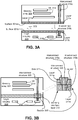
- Figs. 3A-3B illustrate an example process of bonding, using hybrid bonding process, a memory array 304 and logic circuitry 308, thereby forming a bonding interface layer 310, in accordance with some embodiments.
- the memory array 304 of Figs. 3A-3B can be any of the memory arrays 104a, 104b of Fig. 1 (or any other memory array discussed herein)
- the logic circuitry 308 of Figs. 3A-3B can be the logic circuitry 108 of Fig. 1 (or any other logic circuitry discussed herein)
- the bonding interface layer 310 of Figs. 3A-3B can be any of the bonding interface layers 110a, 110b of Fig. 1 (or any other bonding interface layer discussed herein).
- the array 304 comprises example WLs 314.
- Three example logic components 318 of the logic circuitry 308 are symbolically illustrated in Figs. 3A-3B .
- the array 304 and the logic circuitry 308 are formed separately.
- one or both the array 304 and the logic circuitry 308 may be in a wafer level, i.e., part of a corresponding wafer; while in some other embodiments, one or both the array 304 and the logic circuitry 308 may be in a die level (i.e., singulated and separated in individual dies).
- the array 304 has a layer 311a on a bottom surface of the array 304 that is to be bonded to the logic circuitry 308, and the logic circuitry 308 has a layer 311b on a top surface of the logic circuitry that is to be bonded to the array 304a. That is, the layers 311a, 311b are to be bonded.
- the layers 311a, 311b may be similar to the layers 211a, 211b discussed with respect to Figs. 2A-2C .
- the arrows 303 in Fig. 3A symbolically indicate that the array 304 and the logic circuitry 308 are to be bonded.
- a plurality of interconnect structures comprising conductive material extend through the layers 311a, and 311b.
- Fig. 3A illustrates an example interconnect structure 319a comprising conductive material (e.g., such as metal) extends through the layer 311a; and an interconnect structure 319b comprising conductive material (e.g., such as metal) extends through the layer 311b.
- a surface 301a of the layer 311a (e.g., which faces away from the array 304) has a plurality of metal or other conductive materials exposed through the layer 311a (such as the tip of the interconnect structure 319a being exposed through the surface 301a).
- the tip of the interconnect structure 319a is flush or co-planar with the surface 301a of the layer 311a, as illustrated.
- the layer 311a is polished or cleaned, to make the tip of the interconnect structure 319a flush or co-planar with the surface 301a of the layer 311a.
- a surface 301b of the layer 311b (e.g., which faces away from the logic circuitry 208) has a plurality of metal or other conductive materials exposed through the layer 311b (such as the tip of the interconnect structure 319b protruding or exposed through the surface 301b).
- Fig. 3B illustrates a combined structure where the array 304 and logic circuitry 308 have bonded, to form the bonding interface layer 310.
- the bonding between the array 304 and logic circuitry 308 is performed using hybrid bonding.
- hybrid bonding As previously discussed with respect to Figs. 2A-2C , in fusion bonding, the bonding is between the two layers 211a, 211b, without any bonding between metals or other conductive material exposed through the bonding surfaces of these two layers.
- hybrid bonding the layers 311a, 311b are bonded, along with attachment or contact between corresponding conductive materials exposed through the bonding surfaces of these two layers.
- the layers 311a, 311b are bonded, along with attachment, bonding or contact between conductive materials of the tips of the interconnect structures 319a, 319b respectively exposed through the bonding surfaces of the layers 311a, 311b.
- the interconnect structures 319a, 319b are in contact in Fig. 3B , thereby forming a combined interconnect structure 320.
- the smooth surfaces 301a and 301b of the layers 311a, 311b, respectively, and the exposed tips of the interconnect structures 319a, 319b are polished, smoothed, and/or cleaned (e.g., made free of any impurity).
- the layers 311a, 311b are pre-bonded, e.g., at room temperature.
- the layers 311a, 311b are annealed, e.g., at elevated temperature, such that the layers 311a, 311b bond to form the bonding interface layer 310.
- any other appropriate process flow may be employed for the hybrid bonding process.
- the layers 311a, 311b, 310 may be similar to those discussed with respect to Figs. 2A-2C .
- each of the layers 311a, 311b, 310 comprises silicon and oxygen, e.g., comprises Silicon dioxide (SiO 2 ).
- each of the layers 311a, 311b, 310 comprises silicon and nitrogen, e.g., comprises Silicon Nitride (Si 3 N 4 ).
- any other appropriate material, generally used for hybrid bonding may be used for the bonding interface layer 310.
- a thickness of the bonding interface layer 310 is within a range of about 3000 angstrom to 1 micron.
- the layers 311a, 311b are bonded to form the single bonding interface layer 310, where the individual layers 311a, 311b are not separately discernable in the bonding interface layer 310. In another example, the individual layers 311a, 311b are separately discernable in the bonding interface layer 310.
- Fig. 3B further illustrates a magnified view of a section 305, which comprises a section of the bonding interface layer 310 and the interconnect structure 320.
- an imaginary line AA' passes through the bonding interface layer 310, and divides the bonding interface layer 310 into the layers 311a and 311b.
- the interconnect structure 320 passes through the line AA'.
- a side 321 of the interconnect structure 320 is also illustrated.
- the interconnect structure 320 comprises the interconnect structures 319a, 319b. Ideally, if the array 304 and the logic circuitry 308 are perfectly aligned during the bonding process, the interconnect structures 319a, 319b would also be perfectly aligned.
- the array 304 and the logic circuitry 308 may not be perfectly aligned during the bonding process, and hence, the interconnect structures 319a, 319b may also not be perfectly aligned in the interconnect structure 320.
- the magnified view of the section 305 shows misalignment or offset between two sections of the interconnect structure 320 passing through the bonding interface layer 310, as illustrated in Fig. 3B .
- the misalignment or offset may inherently be an unintended consequence of hybrid bonding process. As discussed with respect to Fig. 2C , no such misalignment or offset will be present if the fusion bonding is employed instead.
- the bonding interface layer 310 includes a diffusion barrier for the exposed sections of the interconnect structure 320.
- the bonding interface layer 310 comprises Silicon (Si), Carbon (C), Nitrogen (N), and/or Oxygen (O) (e.g., a Si-C-N-O system), e.g., in addition to, or instead of, the examples of material for the bonding interface layer 310 provided herein previously. That is, the bonding interface layer 210 includes dielectric with composition mixture of silicon, carbon, nitrogen, and/or oxygen, which is used to enable good bonding, as well as to form a diffusion barrier to the misaligned (and hence exposed) metal (e.g., copper) of the interconnect structure 320.
- Si Silicon
- C Carbon
- N Nitrogen
- O Oxygen
- the metal to metal bonding is a via-to-via bonding.
- hybrid bonding can involve via-to-line bonding as well.
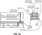
- Fig. 3C illustrates an example process of bonding, using hybrid bonding process, a memory array 304 and logic circuitry 308, thereby forming a bonding interface layer 310, where the hybrid bonding involves a via-to-line bonding, in accordance with some embodiments.
- the interconnect structure 319a includes a via comprising conductive material through the layer 311a
- the interconnect structure 319b includes a conductive line (e.g., metal line) through the layer 311b, and the conductive materials of the via and the lines are bonded during the hybrid bonding process.
- Fig. 4 illustrates a cross-sectional view of an integrated memory structure (also referred to as a structure 400) comprising a first memory array 404a, a second memory array 404b, and logic circuitry 408 between the first and second memory arrays, wherein the logic circuitry 408 is separated from the first and second memory arrays by way of first and second bonding interface layers 410a, 410b, respectively, in accordance with some embodiments.
- the arrays 404a, 404b and the logic circuitry 408 of Fig. 4 respectively correspond to the arrays 104a, 104b and the logic circuitry 108 of Fig. 1 .
- the bonding interface layers 410a, 410b respectively correspond to the bonding interface layers 110a, 110b of Fig. 1 .
- the bonding interface layer 410a is formed via fusion bonding (e.g., as discussed with respect to Figs. 2A-2C ) of the array 404a and the logic circuitry 408, and the bonding interface layer 410b is formed via fusion bonding of the array 404b and the logic circuitry 408.
- the bonding interface layers 410a, 410b are similar to the bonding interface layer 210 of Figs. 2A-2C .
- the bonding interface layers 410a, 410b comprise oxide material such as Silicon dioxide (SiO 2 ), nitride material such as Silicon Nitride (Si 3 N 4 ), etc., although any other appropriate material that are used for bonding two wafer level components may also be used.
- a thickness of each of the bonding interface layers 410 is within a range of about 3000 angstrom to 1 micron.
- the memory array 404b is formed on a substrate 479.
- the substrate 479 in an example, is a wafer on which multiple such arrays are formed.
- the bonding process is performed while the array 404b is still on the wafer, i.e., prior to dicing of the wafer. In another example, the bonding process is performed after the dicing of the wafer.
- the array 404a includes memory cells, such as NAND flash memory cells, formed at memory pillars 456a.
- the array 404a further includes conductive access lines to enable access to the memory cells, such as bitlines 464a, e.g., which are coming out of the page in Fig. 4 (e.g., perpendicular to a plane of the paper), wordlines (WL) 420a, select gate source (SGS) 452a, and select gate drain (SGD) 460a.
- the wordlines 420a are staggered or arranged in a stair-case like pattern.
- the array 404a further includes current common source (SRC, also referred to as a source plate) 455a, located underneath the memory pillars 456a.
- SRC current common source
- the array 404a further includes WL connection terminals 457a, each WL connection terminal 457a coupled to a corresponding WL 420a, e.g., via interconnect structures 459a.
- the array 404a further includes SDG connection terminals 461a, each SGD connection terminal 459a coupled to a corresponding SGD 460a, e.g., via interconnect structures 459a.
- the array 404a comprises a plurality of metallization levels 407a comprising metals, which electrically couple various components within the array 404a.
- the structure 400 is accessed from a top surface 403a of the array 404a.
- the array 404a comprises a plurality of interconnect structures 407a comprising one or more metallization levels.
- Interconnect terminals 402 are coupled to the surface of the array 404a, e.g., for connecting the structure 400 to external components.
- one or more interconnect structures 411 pass through the array 404a and the bonding interface layer 410a, e.g., to electrically couple to the logic circuitry 408 and/or the array 404b.
- the interconnect structures 411 can be used to transmit signals to and/or from the logic circuitry 408 and/or the array 404b.
- the array 404b has a structure that is at least in part similar to the structure of the array 404a.
- the array 404b includes memory cells, such as NAND flash memory cells, formed at memory pillars 456b.
- the array 404b further includes conductive access lines to enable access to the memory cells, such as bitlines 464b, WL 420b, SGS 452b, and SGD 460b.
- the array 404b further includes SRC 455b, located underneath the memory pillars 456b.
- the array 404b further includes WL connection terminals 457b, each WL connection terminal 457b coupled to a corresponding WL 420b, e.g., via interconnect structures 459b.
- the array 404b further includes SDG connection terminals 461b coupled to a corresponding SGD 460b, e.g., via interconnect structures 459b.
- various interconnect structures 413 pass through the array 404a and the bonding interface layer 410b, and these interconnect structures 413 transmit access lines signals to and/or from the logic circuitry 408 and/or the array 404b.
- interconnect structures 413a transmit SGD signals to and/or from SGD 460b of the array 404b (although merely two such interconnect structures 413a are illustrated in Fig. 4 ).
- interconnect structures 413b transmit wordline signals to and/or from WLs 420b of the array 404b.
- interconnect structures 413c transmit SGS signals to and/or from SGS 452b of the array 404b.
- Interconnect structure 413d transmits SRC signals to and/or from SRC 455b of the array 404b.
- Interconnect structure 413e transmits bitline signals to and/or from bitlines 464b of the array 404b.
- at least the interconnect structures 411, 413 extend through the bonding interface layer 410a.
- the logic circuitry 408 includes various logic circuits, generally illustrated as logic components 418a, 418b, 418c.
- logic components 418 include, but are not limited to, address decoders, state machines, buffers, word line drivers, bit line drivers, sense amplifiers, voltage dividers, charge pumps, digital logic blocks, etc.
- one or more of the logic components 418 include CMOS logic.
- the logic circuitry 408 include high voltage logic components (e.g., components and/or transistors that operate at a relatively high voltage, such as in the range of 5 V to 30 V) and/or low voltage logic components (e.g., components and/or transistors that operate at a relatively low voltage, such as in the range of 0.9 V to 5 V).
- the logic circuitry 408 includes n-channel metal-oxide semiconductor field-effect transistors (MOSFET), p-channel MOSFETs, or both.
- interconnect structures 415 couple the logic circuitry 408 to the array 404b.
- the interconnect structures 415 extend through the bonding interface layer 410b, thereby coupling the logic circuitry 408 and the array 404b.
- FIG. 4 Also illustrated in Fig. 4 is a magnified view of a section 425, where the section 425 includes a section of the bonding interface layer 410a and an interconnect structure 413 extending through the bonding interface layer 410a.
- the interconnect structure 413 extending through the bonding interface layer 410a does not have any discontinuity, offset or misalignment, e.g., as the array 404a and the logic circuitry 408 are bonded using fusion bonding in an example.
- FIG. 4 Also illustrated in Fig. 4 is a magnified view of a section 427, where the section 427 includes a section of the bonding interface layer 410b and an interconnect structure 415 extending through the bonding interface layer 410b.
- the interconnect structure 415 extending through the bonding interface layer 410b does not have any discontinuity, offset or misalignment, e.g., as the array 404b and the logic circuitry 408 are bonded using fusion bonding in an example.
- the bonding interface layer 410a separates the array 404a and the logic circuitry 408.
- the structure 400 has a left sidewall 403m and an opposing right sidewall 403n (although “left” and “right” are merely for purposes of ease of identification, and not limiting), and the bonding interface layer 410a extends from the left sidewall 403m to the right sidewall 403n.
- the structure 400 has a front wall and an opposing back wall (e.g., which are not visible and not labelled in Fig. 4 , and which are perpendicular to the left and right sidewalls), and the bonding interface layer 410a extends from the front and back walls.
- the structure 400 has a top surface and a bottom surface, and a plurality of walls or surfaces extending between the top and bottom surfaces - the bonding interface layer 410a divides the structure in its entirety such that the bonding interface layer 410a extends to each of the plurality of walls or surfaces.
- the bonding interface layer 410b also divides the structure 400 in its entirety such that the bonding interface layer 410b extends to each of the plurality of walls or surfaces.
- a first die includes the array 404a
- a second dies includes the logic circuitry 408, and
- a third die includes the array 404b, where the three dies are bonded using the bonding interface layers 410a, 410b, as discussed herein.
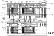
- Figs. 5A , 5B , 5C , 5D , 5E , and 5F collectively illustrate a method for forming a memory structure (such as the memory structure 400 of Fig. 4 ) comprising a first memory array (e.g., memory array 404a), a second memory array (e.g., memory array 404b), and logic circuitry (e.g., logic circuitry 408) interposed between the first and second memory arrays, wherein a first bonding interface layer (e.g., bonding interface layer 410a) is between the first memory array and the logic circuitry, and a second bonding interface layer (e.g., bonding interface layer 410b) is between the second memory array and the logic circuitry, in accordance with some embodiments.
- a first bonding interface layer e.g., bonding interface layer 410a
- a second bonding interface layer e.g., bonding interface layer 410b
- the memory array 404b formed on the substrate 479.
- the substrate 479 in an example, is a wafer on which the array 404b is formed.
- the array 404 also comprises a layer 501a on a surface that is to be bonded with the logic circuitry 408, where the layer 501a may be similar to the layer 211a of Fig. 2A .
- the substrate 502 in an example, is a wafer on which the logic circuitry 408 is formed, e.g., if the logic circuitry 408 is still on a wafer while bonding with the array 404b.
- the substrate 502 is a substrate of a die comprising the logic circuitry 408, e.g., if the die comprising the logic circuitry 408 is to be bonded with the array 404b.
- the logic circuitry 408 also comprises a layer 501b on a surface that is to be bonded with the array 404b, where the layer 501b may be similar to the layer 211b of Fig. 2A .
- the logic circuitry 408 is bonded with the array 404b, e.g., as discussed with respect to Fig. 2B .
- the layers 501a, 501b are bonded to form the bonding interface layer 410b.
- a height of the logic circuitry 408 is HI, as illustrated.
- the support substrate 502 is then de-bonded from the logic circuitry 408.
- various conductive structures or interconnect structures 513, 415, etc. are formed in the logic circuitry 408.
- Some of the conductive structures comprises conductive material (such as metal) deposited within vias that extend through the bonding interface layer 410b, such as conductive structures 415.
- conductive material such as metal
- the interconnect structures 415 are formed after formation of the bonding interface layer 410b, there are no offset or misalignment in the interconnect structures 415, as illustrated in the magnified view of the section 427.
- the logic circuitry 408 comprises a surface 515 that is opposite to the surface of the logic circuitry 408 to which the array 404b is bonded (e.g., the surface 515 was attached to the support substrate 502 in Fig. 5A ). Some of the interconnect structures have ends adjacent to, or exposed through, the surface 515 of the logic circuitry 408. In an example embodiment, the interconnect structures 415, 513 are formed by accessing the logic circuitry 408 through the surface 515. In an example embodiment, various metallization levels, vias, interconnect structures are formed within the logic circuitry 408, resulting in an increase of a height of the logic circuitry 408. For example, in Figs. 5A-5B , the height of the logic circuitry 408 is HI, whereas after formation of the interconnect structures the height increases to H2 in Fig. 5C .
- layer 510c is formed on the surface 515 of the logic circuitry 408, where the layer 510c is similar to the layers 211 of Fig. 2A .
- the array 404a is also illustrated in Fig. 5D, with a layer 501d formed on a surface that is to be bonded to the logic circuitry 408.
- the array 404a may be supported by a support substrate 552, which may be a wafer for example (e.g., if the wafer supporting the array 404a has not been diced yet).
- the layer 510d is similar to the layers 211 of Fig. 2A .
- a height of the array 404a is H3, as illustrated in Fig. 5D . Note that for purposes of illustrative clarity, some of the components of the array 404a, which are labelled in Fig. 4 , are not labelled in Fig. 5D (or in some of the subsequent figures).
- the logic circuitry 408 is bonded with the array 404a, e.g., as discussed with respect to Fig. 2B , and the support substrate 552 is de-bonded from the array 404a.
- the layers 501c, 501d are bonded to form the bonding interface layer 410a.
- interconnect structures 411, 413 are formed in the array 404a, e.g., using deep via etch.
- deep through hole vias are formed that extends through the array 404a and the bonding interface layer 410a, and are filled with conductive material, such as metal, to form the interconnect structures 411, 413.
- a through hole via is formed over a corresponding interconnect structure 513 of the logic circuitry 408 (e.g., where the interconnect structure 513 is formed in Fig. 5C ), such that the conductive material within the via and the interconnect structure 513, in combination, form the interconnect structure 413.
- various metallization levels, various terminals are formed near a top of the array 404a, e.g., which extends a height of the array 404a.
- the array 404a in Fig. 5F has a height H4 that is greater than the height H3 of the array 404a in Fig. 5E . That is, at least a section of the array 404a is formed after the array 404a is bonded with the logic circuitry 408.
- the resultant structure 400 of Fig. 5F is similar to the structure 400 of Fig. 4 .
- the array 404b and the logic circuitry 408 of the structure 400 are bonded using fusion bonding, and the logic circuitry 408 and the array 404a are also bonded using fusion bonding.
- interconnect structures extending through a bonding interface layer 410 is formed after the corresponding components are bonded.
- one or both the bonding in the structure 400 may be hybrid bonding (e.g., as discussed with respect to Figs. 3A-3E ).
- the interconnect structures are pre-formed through the layers 501a, 501b and/or layers 501c, 501d, and the hybrid bonding bonds the corresponding interconnect structures.
- Fig. 6 illustrates a cross-sectional view of a memory structure 600 (also referred to as a structure 600) comprising a memory array 604 and logic circuitry 608, wherein a bonding interface layer 610 is interposed between the memory array 604 and the logic circuitry 608, in accordance with some embodiments.
- a memory structure 600 also referred to as a structure 600
- a bonding interface layer 610 is interposed between the memory array 604 and the logic circuitry 608, in accordance with some embodiments.
- the memory array 604 of Fig. 6 is at least in part similar to the memory array 404a of Fig. 4 , and accordingly, similar components in the two memory arrays are labelled using similar labels, and also individual components within the memory array 604 of Fig. 6 are not discussed in detail.
- the logic circuitry 608 of Fig. 6 is at least in part similar to the logic circuitry 408 of Fig. 4 , and accordingly, similar components in the two logic circuitries are labelled using similar labels, and also individual components within the logic circuitry 608 of Fig. 6 are not discussed in detail.
- the logic circuitry 408 was interposed between two arrays 404a, 404b.
- the logic circuitry 608 of Fig. 6 is bonded to a single array 604.
- the bonding between the logic circuitry 608 and the array 604 is performed using fusion bonding, thereby forming the bonding interface 610 (e.g., which is similar to the bonding interfaces 410 of Fig. 4 ).
- the logic circuitry 408 is formed on a substrate 679.
- Figs. 7A , 7B , and 7C collectively illustrate a method for forming a memory structure (such as the memory structure 600 of Fig. 6 ) comprising a memory array (e.g., memory array 604) and logic circuitry (e.g., logic circuitry 608 of Fig. 6 ), wherein a bonding interface layer (e.g., bonding interface layer 610) is between the memory array and the logic circuitry, in accordance with some embodiments.
- a bonding interface layer e.g., bonding interface layer 610
- FIG. 7A illustrated is the logic circuitry 608 on a substrate 679.
- a layer 501b similar to the layers 211 of Fig. 2A , is deposited on the logic circuitry 608.
- the array 604 which may be similar to the array 404a of Fig. 5D .
- the logic circuitry 408 and the array 604 are not yet bonded in Fig. 7A .
- the array 604 is bonded with the logic circuitry 608 using fusion bonding, as discussed with respect to Fig. 5E . Accordingly, the bonding interface layer 610 is formed due to the bonding of the layers 501a, 501b.
- interconnect structures 411, 413 are formed in the array 604, e.g., using deep via etch, as discussed with respect to Fig. 5E .
- various metallization levels, various terminals e.g., such as WL connection terminals 457a, SDG connection terminals 461a, etc.
- various terminals are formed near a top of the array 604, e.g., which extends a height of the array 604.
- the array 604 in Fig. 7C has a height H4 that is greater than the height H3 of the array 604 in Fig. 7B , e.g., as discussed with respect to Fig. 5E .
- the resultant structure of Fig. 7C is the structure 600 of Fig. 6 .
- Fig. 8 illustrates a cross-sectional view of a memory structure 800 (also referred to as a structure 800) comprising a first memory array 804a, a second memory array 804b, and logic circuitry 808, wherein a bonding interface layer 810 is interposed between the second memory array 804b and the logic circuitry 608, without any such bonding interface layer between the first memory array 804a and the logic circuitry 808, in accordance with some embodiments.
- a bonding interface layer 810 is interposed between the second memory array 804b and the logic circuitry 608, without any such bonding interface layer between the first memory array 804a and the logic circuitry 808, in accordance with some embodiments.
- the memory arrays 804a, 804b of Fig. 8 are at least in part similar to the memory arrays 404a, 404b, respectively, of Fig. 4 , and accordingly, similar components within the memory arrays in the two figures are labelled using similar labels, and also individual components within the memory arrays 804a, 804b of Fig. 8 are not discussed in detail.
- the logic circuitry 808 of Fig. 8 is at least in part similar to the logic circuitry 408 of Fig. 4 , and accordingly, similar components in the two logic circuitries are labelled using similar labels, and also individual components within the logic circuitry 808 of Fig. 8 are not discussed in detail.
- the logic circuitry 808 of Fig. 8 is at least in part formed along with the formation of the memory array 804a. That is, the logic circuitry 808 is bot bonded with the memory array 804a - rather, the logic circuitry 808 is formed in situ with the memory array 804a, as will be discussed herein in further detail in turn.
- the array 804a and the logic circuitry 808 are in a single die, whereas the array 804b is in a different die.
- the combination of the memory array 804a and the logic circuitry 808 is bonded to the memory array 804b, via the bonding interface layer 810.
- the bonding interface layer 810 is at least in part similar to the bonding interface layers 410 of Fig. 4 .
- a layer 815 is between the bonding interface layer 810 and the logic circuitry 808.
- the bonding interface layer 810 substantially extends from the sidewall 403n to the sidewall 403m, and the layer 815 also substantially extends from the sidewall 403n to the sidewall 403m.
- the layer 815 substantially covers (e.g., covers more than 90%, or more than 95%, or more than 99%) a bottom surface of the logic circuitry 808, and the bonding interface layer 810 substantially covers a bottom surface of the layer 815.
- the layer 815 comprises silicon, e.g., crystalline silicon.
- the layer 815 is remnant of a wafer or substrate on which the combination of the array 804a and the logic circuitry 808 are formed, as will be discussed in further detail in turn.
- Figs. 9A , 9B , 9C , and 9D collectively illustrate a method for forming a memory structure (such as the memory structure 800 of Fig. 8 ) comprising a first memory array (e.g., array 804a), a second memory array (e.g., array 804b), and logic circuitry (e.g., logic circuitry 808), wherein a bonding interface layer (e.g., bonding interface layer 810) is interposed between the second memory array and the logic circuitry, without any such bonding interface layer between the first memory array and the logic circuitry, in accordance with some embodiments.
- a bonding interface layer e.g., bonding interface layer 810
- a temporary carrier wafer 919 is attached to a top surface of the combination of the array 804a and the logic circuitry 808 (e.g., where an opposite bottom surface of the combination of the array804a and the logic circuitry 808 has the wafer 915 attached thereon). Subsequently, the wafer 915 is polished or otherwise thinned, to decrease a height of the wafer 915, thereby forming the layer 815.
- the original height of the wafer 915 is Hw1
- the wafer 915 is thinned such that a height of the layer 815 in Fig. 9B is Hw2, where Hw2 is less than Hw1.
- the height Hw2 of the layer 815 is in the range of 7 microns to 10 microns.
- layer 901a is deposited on a bottom surface of the layer 815. Also, illustrated in Fig. 9C is the array 804b, with layer 901b deposited on a top surface of the array 804b.
- the layers 901a, 901b are similar to the layers 501 of Fig. 5A .
- vias are formed through the layers 901a, 815, and filled with conductive material such as metal, to form interconnection structures 915a through the layers 901a, 815.
- the combination of the array 804a and the logic circuitry 808 is accessed from the bottom surface (e.g., from the exposed surface of the layer 901a) while forming the vias for the interconnection structures 915a.
- interconnection structures 915b through the layer 901b.
- the array 804b is accessed from the top surface (e.g., from the exposed surface of the layer 901a) while forming the vias for the interconnection structures 915b.
- each of the layers 901a and 901b have openings through which tips of the corresponding interconnect structures 915a, 915b are exposed (e.g., similar to that discussed with respect to Figs. 3A-3B ).
- the conductive material of the tips of the interconnect structures 915a exposed through the layer 901a and the bottom surface of the layer 901a are flush or co-planar.
- the bottom surface of the layer 901a is polished, to that tips of the interconnect structures 915a exposed through the layer 901a and the bottom surface of the layer 901a are flush or coplanar.
- the conductive material of the tips of the interconnect structures 915b exposed through the layer 901a and the bottom surface of the layer 901a are flush or at the same level, i.e., coplanar.
- the layers 901a and 901b are bonded to form the bonding interface layer 810.
- two corresponding interconnect structures 915a, 915b are also bonded or otherwise come in contact, to form a common interconnect structure 415.
- the bonding is between the layers 901a, 901b, as well as between corresponding ones of the interconnect structures 915a, 915b - accordingly, as discussed with respect to Figs. 3A-3B
- the bonding of Fig. 9D is a hybrid bonding.
- FIG. 9D which is illustrated in a magnified view of a section 427.
- Fig. 9D illustrates multiple via-to-via bonding through the layer 810 (e.g., as discussed with respect to Figs. 3A-3B ), there may be via-to-line bonding as well through the layer 810 (e.g., as discussed with respect to Fig. 3C ).
- the resultant structure of Fig. 9D is the structure 800 of Fig. 8 .
- Fig. 10 illustrates an example computing system implemented with integrated memory structures disclosed herein, in accordance with one or more embodiments of the present disclosure.
- the computing system 2000 houses a motherboard 2002.
- the motherboard 2002 may include a number of components, including, but not limited to, a processor 2004 and at least one communication chip 2006, each of which can be physically and electrically coupled to the motherboard 2002, or otherwise integrated therein.
- the motherboard 2002 may be, for example, any printed circuit board, whether a main board, a daughterboard mounted on a main board, or the only board of system 2000, etc.
- computing system 2000 may include one or more other components that may or may not be physically and electrically coupled to the motherboard 2002.
- these other components may include, but are not limited to, volatile memory (e.g., DRAM), non-volatile memory (e.g., ROM, flash memory such as 3D NAND flash memory), a graphics processor, a digital signal processor, a crypto processor, a chipset, an antenna, a display, a touchscreen display, a touchscreen controller, a battery, an audio codec, a video codec, a power amplifier, a global positioning system (GPS) device, a compass, an accelerometer, a gyroscope, a speaker, a camera, and a mass storage device (such as hard disk drive, compact disk (CD), digital versatile disk (DVD), and so forth).
- multiple functions can be integrated into one or more chips (e.g., for instance, note that the communication chip 2006 can be part of or otherwise integrated into the processor 2004).
- Any memory such as any flash memory (e.g., a 3D NAND flash memory), included in computing system 2000 may include one or more memory arrays bonded with logic circuitry, as discussed herein.
- the logic circuitry is interposed between, and shared among, two memory arrays, as discussed herein.
- the communication chip 2006 enables wireless communications for the transfer of data to and from the computing system 2000.
- wireless and its derivatives may be used to describe circuits, devices, systems, methods, techniques, communications channels, etc., that may communicate data through the use of modulated electromagnetic radiation through a non-solid medium. The term does not imply that the associated devices do not contain any wires, although in some embodiments they might not.
- the communication chip 2006 may implement any of a number of wireless standards or protocols, including, but not limited to, Wi-Fi (IEEE 802.11 family), WiMAX (IEEE 802.16 family), IEEE 802.20, long term evolution (LTE), Ev-DO, HSPA+, HSDPA+, HSUPA+, EDGE, GSM, GPRS, CDMA, TDMA, DECT, Bluetooth, derivatives thereof, as well as any other wireless protocols that are designated as 3G, 4G, 5G, and beyond.
- the computing system 2000 may include a plurality of communication chips 2006.
- a first communication chip 2006 may be dedicated to shorter range wireless communications such as Wi-Fi and Bluetooth and a second communication chip 2006 may be dedicated to longer range wireless communications such as GPS, EDGE, GPRS, CDMA, WiMAX, LTE, Ev-DO, and others.
- the processor 2004 of the computing system 2000 includes an integrated circuit die packaged within the processor 2004.
- the term "processor” may refer to any device or portion of a device that processes, for instance, electronic data from registers and/or memory to transform that electronic data into other electronic data that may be stored in registers and/or memory.
- the communication chip 2006 also may include an integrated circuit die packaged within the communication chip 2006.
- multi-standard wireless capability may be integrated directly into the processor 2004 (e.g., where functionality of any chips 2006 is integrated into processor 2004, rather than having separate communication chips).
- processor 2004 may be a chip set having such wireless capability.
- any number of processor 2004 and/or communication chips 2006 can be used.
- any one chip or chip set can have multiple functions integrated therein.
- the computing system 2000 may be a laptop, a netbook, a notebook, a smartphone, a tablet, a personal digital assistant (PDA), an ultra-mobile PC, a mobile phone, a desktop computer, a server, a printer, a scanner, a monitor, a set-top box, an entertainment control unit, a digital camera, a portable music player, a digital video recorder, or any other electronic device that processes data or employs one or more integrated circuit structures or devices, as variously described herein.
- PDA personal digital assistant
Landscapes
- Engineering & Computer Science (AREA)
- Microelectronics & Electronic Packaging (AREA)
- Semiconductor Memories (AREA)
- Non-Volatile Memory (AREA)
- Manufacturing & Machinery (AREA)
Abstract
Description
- Flash memory, such as NAND flash memory, is a nonvolatile storage medium. A flash memory array generally is coupled to logic circuits that facilitate operations of the memory array. The logic circuits have components such as word line drivers, bit line drivers, and sense amplifiers for the memory array. The logic circuits, for example, include complementary metal-oxide-semiconductor (CMOS) logic. Often times, thermal cycles of the process for formation of the memory array adversely affect the logic circuits. As will be appreciated in light of this disclosure and explained in turn, there exists a number of non-trivial issues associated with decreasing complexity, power consumption, and/or cost (e.g., cost per bit of memory) of the logic circuits, as well as avoiding the adverse effects of thermal cycles of the memory array processing on the logic circuits.
-
-
Fig. 1 illustrates a cross-sectional view of an integrated memory structure comprising a first memory array, a second memory array, and logic circuitry, wherein a first bonding interface layer is between the first memory array and the logic circuitry, and a second bonding interface layer is between the second memory array and the logic circuitry, in accordance with some embodiments. -
Figs. 2A-2C illustrate an example process of bonding, using a fusion bonding process, a memory array and logic circuitry, thereby forming a bonding interface layer between the memory array and the logic circuitry, in accordance with some embodiments. -
Figs. 3A-3B illustrate an example process of bonding, using a hybrid bonding process, a memory array and logic circuitry, thereby forming a bonding interface layer between the memory array and the logic circuitry, in accordance with some embodiments. -
Fig. 3C illustrates an example process of bonding, using hybrid bonding process, a memory array and logic circuitry, thereby forming a bonding interface layer, where the hybrid bonding involves a via-to-line bonding, in accordance with some embodiments. -
Fig. 4 illustrates a cross-sectional view of an integrated memory structure comprising a first memory array, a second memory array, and logic circuitry between the first and second memory arrays, wherein the logic circuitry is separated from the first and second memory arrays by way of first and second bonding interface layers, respectively, in accordance with some embodiments. -
Figs. 5A ,5B ,5C ,5D ,5E , and5F collectively illustrate a method for forming a memory structure comprising a first memory array, a second memory array, and logic circuitry interposed between the first and second memory arrays, wherein a first bonding interface layer is between the first memory array and the logic circuitry, and a second bonding interface layer is between the second memory array and the logic circuitry, in accordance with some embodiments. -
Fig. 6 illustrates a cross-sectional view of a memory structure comprising a memory array and logic circuitry, wherein a bonding interface layer is interposed between the memory array and the logic circuitry, in accordance with some embodiments. -
Figs. 7A ,7B , and7C collectively illustrate a method for forming a memory structure comprising a memory array and logic circuitry, wherein a bonding interface layer is between the memory array and the logic circuitry, in accordance with some embodiments. -
Fig. 8 illustrates a cross-sectional view of a memory structure comprising a first memory array, a second memory array, and logic circuitry, wherein a bonding interface layer is interposed between the second memory array and the logic circuitry, without any such bonding interface layer between the first memory array and the logic circuitry, in accordance with some embodiments. -
Figs. 9A ,9B ,9C , and9D collectively illustrate a method for forming a memory structure comprising a first memory array, a second memory array, and logic circuitry, wherein a bonding interface layer is interposed between the second memory array and the logic circuitry, without any such bonding interface layer between the first memory array and the logic circuitry, in accordance with some embodiments. -
Fig. 10 illustrates an example computing system implemented with one or more integrated memory structures disclosed herein, in accordance with one or more embodiments of the present disclosure. - An integrated memory structure is disclosed herein, which includes multiple memory arrays, such as flash memory arrays, sharing a common logic circuitry. In some embodiments, the shared logic circuitry is interposed between a first memory array and a second memory array. In an example, the first memory array and the second memory array are processed and formed separately from the logic circuitry. Subsequent to formation of the memory arrays and the logic circuitry, the logic circuitry is bonded to the first memory array and the second memory array. Thus, in an example, the integrated memory structure includes a first die comprising the first memory array, a second die comprising the second memory array, and a third die comprising the logic circuitry, where the third die is between the first and second dies, and the third die is bonded to each of the first and second dies.
- In an example, a first layer is deposited on a surface of the logic circuitry that is to be bonded with the memory array, and a second layer is deposited on a surface of the memory array that is to be bonded with the logic circuitry. Each of the first and second layer comprises, for example, an oxide material (such as silicon dioxide), a nitride material (such as silicon nitride), an oxynitride material (such as silicon oxynitride), and/or the like. The first and second layers are cleaned and polished, pre-bonded with one another, and annealed at an elevated temperature, thereby bonding the first and second layers to form a bonding interface layer. Thus, in the integrated memory structure, the logic circuit and the memory array are separated by the bonding interface layer. As discussed, the bonding interface layer comprises silicon dioxide, silicon nitride, silicon oxynitride, or other suitable electrically-insulating bonding material. Although the thickness of the bonding interface layer can vary, in some embodiments it has a thickness in the range of 3000 angstroms to 10 microns. Thus, in the integrated memory structure that includes logic circuitry between, and bonded to, two memory arrays, a first bonding interface layer is between the logic circuitry and a first memory array, and a second bonding interface layer is between the logic circuitry and a second memory array.
- In some examples, the bonding between the logic circuitry and a memory array may be formed using fusion bonding or hybrid bonding. As will be discussed in further detail in turn, in fusion bonding, the bonding process is between the first and second layers (and not between any conductive material such as metal). For example, in fusion bonding (which is also referred to as direct bonding), no conductive structure (e.g., vias including metal) extends through the first and second layers, while these layers are being bonded to form the bonding interface layer. After the bonding is completed, via holes are formed extending through the bonding interface layer and are filled with metal, thereby forming interconnect structures between the logic circuitry and the memory array through the bonding interface layer. Because the vias are formed through the bonding interface layer subsequent to the first and second layers being bonded, sections of an interconnect structure extending through the bonding interface layer do not have any misalignment or offset (no unlanded portions), as will be discussed in further detail in turn.
- In contrast to fusion bonding and as will be discussed in further detail in turn, in hybrid bonding, the bonding process is between the first and second layers and also between conductive structures within the first layer and conductive structures within the second layer. For example, in hybrid bonding, conductive structure (e.g., a via including metal) extends through each of the first and second layers, prior to these layers being bonded to form the bonding interface layer. For example, a first interconnect structure extends through the first layer and is exposed through, and flush with, a surface of the first layer; and a second interconnect structure extends through the second layer and is exposed through, and flush with, a surface of the second layer (e.g., prior to the bonding process). During the bonding process, surfaces of the first layer and the second layers bond to form a bonding interface layer, along with a bonding or contact of the first interconnect structure and the second interconnect structure. In an example, due to unintentional practical considerations of the bonding process, the memory array and the logic circuitry may not be perfectly aligned during the bonding process, and hence, the first interconnect structure and the second interconnect structure may not be perfectly aligned while being bonded. Accordingly, sections of a combined interconnect structure formed through the bonding or contact of the first and second interconnect structures, which extend through the bonding interface layer, may have some misalignment or offset, as will be discussed in further detail in turn.
- Bonding the logic circuitry with two memory arrays and sharing the logic circuitry among the two memory arrays have several advantages. For example, sharing the logic circuitry among the memory arrays reduces complexity and/or power consumption of the logic circuitry. For example, a single shared voltage divider block of the logic circuitry can be used for both the memory arrays. Sharing the logic circuitry among the memory arrays also reduces cost of the logic circuitry per bit of memory. Thus, the cost of the logic circuitry is amortized across two memory arrays, thereby resulting in cost savings. Also, due to the use of the bonding process between the logic circuitry and the memory arrays, it is possible to separate the logic circuitry processing from the memory array processing, so that the logic circuitry is not affected by the thermal cycles of the process of memory array formation. Also, forming the memory arrays and the logic circuitry independently and separately reduces overall cycle time to manufacture the integrated memory structure.
- Instead of bonding the logic circuitry with each of the two memory arrays according to some embodiments, in another example embodiment, the logic circuitry can be bonded with a single memory array. For example, the memory array and the logic circuitry are formed separately and then bonded (e.g., using fusion bonding or hybrid bonding). Thus, formation of the logic circuitry is separate from formation of the memory array, so that the logic circuitry is not affected by thermal cycles of the process of memory array formation.
- In an example embodiment, instead of bonding the logic circuitry with each of two memory arrays, the logic circuitry is formed to be integrated with a first memory array (e.g., instead of bonding separately formed logic circuitry and the first memory array, a combined structure is formed that includes both the logic circuitry and the first memory array). After the combination of the first memory array and the logic circuitry is formed, the combination is then bonded with a second memory array. In the final memory structure, the logic circuitry is interposed between the first and second memory arrays. A bonding interface layer is between the logic circuitry and the second memory array (in other words, the combination of the first memory array and the logic circuitry is bonded with the second memory array). However, no such bonding interface layer is present between the logic circuitry and the first memory array. This alternate forming process still allows the logic circuitry to be shared among the first and second memory arrays, thereby reducing complexity, power consumption, and/or a cost per bit of the logic circuitry, as previously discussed herein.
- As discussed herein, terms referencing direction, such as upward, downward, vertical, horizontal, left, right, front, back, etc., are used for convenience to describe embodiments of integrated circuits having a base or substrate extending in a horizontal plane. Embodiments of the present disclosure are not limited by these directional references and it is contemplated that integrated circuits and device structures in accordance with the present disclosure can be used in any orientation.
- Materials that are "compositionally different" or "compositionally distinct" as used herein refers to two materials that have different chemical compositions. This compositional difference may be, for instance, by virtue of an element that is in one material but not the other (e.g., SiGe is compositionally different than silicon), or by way of one material having all the same elements as a second material but at least one of those elements is intentionally provided at a different concentration in one material relative to the other material (e.g., SiGe having 70 atomic percent germanium is compositionally different than from SiGe having 25 atomic percent germanium). In addition to such chemical composition diversity, the materials may also have distinct dopants (e.g., gallium and magnesium) or the same dopants but at differing concentrations. In still other embodiments, compositionally distinct materials may further refer to two materials that have different crystallographic orientations. For instance, (110) silicon is compositionally distinct or different from (100) silicon. Creating a stack of different orientations could be accomplished, for instance, with blanket wafer layer transfer.
- Note that, as used herein, the expression "X includes at least one of A or B" refers to an X that may include, for example, just A only, just B only, or both A and B. To this end, an X that includes at least one of A or B is not to be understood as an X that requires each of A and B, unless expressly so stated. For instance, the expression "X includes A and B" refers to an X that expressly includes both A and B. Moreover, this is true for any number of items greater than two, where "at least one of' those items are included in X. For example, as used herein, the expression "X includes at least one of A, B, or C" refers to an X that may include just A only, just B only, just C only, only A and B (and not C), only A and C (and not B), only B and C (and not A), or each of A, B, and C. This is true even if any of A, B, or C happens to include multiple types or variations. To this end, an X that includes at least one of A, B, or C is not to be understood as an X that requires each of A, B, and C, unless expressly so stated. For instance, the expression "X includes A, B, and C" refers to an X that expressly includes each of A, B, and C. Likewise, the expression "X included in at least one of A or B" refers to an X that may be included, for example, in just A only, in just B only, or in both A and B. The above discussion with respect to "X includes at least one of A or B" equally applies here, as will be appreciated.
- Elements referred to herein with a common reference label followed by a particular number or alphabet may be collectively referred to by the reference label alone. For example, in
Fig. 1 discussed herein later,memory arrays -
Fig. 1 illustrates a cross-sectional view of an integrated memory structure 100 (also referred to as a structure 100) comprising a first memory array (also referred to as an "array") 104a, asecond memory array 104b, andlogic circuitry 108, wherein a first bonding interface layer 110a is between thefirst array 104a and thelogic circuitry 108, and a second bonding interface layer 110b is between thesecond array 104b and thelogic circuitry 108, in accordance with some embodiments. - In an example, each of the
arrays memory arrays 3D memory arrays - The
array 104a comprises word lines (WLs) 114a, and thearray 104b comprisesWLs 114b. Although three WLs are illustrated for each of the arrays 104, the arrays can have any appropriate number of WLs. - Three
example logic components 118 of thelogic circuitry 108 are symbolically illustrated inFig. 1 . Examples oflogic components 118 include, but are not limited to, address decoders, state machines, buffers, word line drivers, bit line drivers, sense amplifiers, voltage dividers, charge pumps, digital logic blocks, logic gates, switches, inverters, adders, multipliers, etc. In an example, one or more of thelogic components 118 include complementary metal-oxide-semiconductor (CMOS) logic. In an example, thelogic circuitry 108 may also be referred to as "CMOS logic," "CMOS circuitry," and/or the like, due to presence of CMOS circuits within thelogic circuitry 108. In an example, thelogic circuitry 108 includes high voltage logic components (e.g., components and/or transistors that operate at a relatively high voltage, such as in the range of 5 V to 30 V) and/or low voltage logic components (e.g., components and/or transistors that operate at a relatively low voltage, such as in the range of 0.9 V to 5 V). - The
structure 100 is symbolically illustrated in high level inFig. 1 , without illustrating various internal components within thearrays arrays logic circuitry 108 will be discussed in turn. - As will be discussed in further detail in turn, the
array 104a, thearray 104b, and thelogic circuitry 108 are formed and processed separately. Subsequently, thearray 104a and thelogic circuitry 108 are bonded (e.g., using wafer to wafer bonding, die to die bonding, wafer to die bonding, or die to wafer bonding), thereby forming the bonding interface layer 110a. Thus, in an example, bonding thearray 104a and thelogic circuitry 108 is accomplished by bonding the wafers together that include these components, and then dicing the wafers (e.g., wafer to wafer bonding). In another example, bonding thearray 104a and thelogic circuitry 108 is accomplished by bonding a die comprising thearray 104a and a die comprising the logic circuitry 108 (e.g., die to die bonding). In yet another example, bonding thearray 104a and thelogic circuitry 108 is accomplished by bonding a wafer comprising thearray 104a and a die comprising thelogic circuitry 108, and then dicing the wafer (e.g., wafer to die bonding). In yet another example, bonding thearray 104a and thelogic circuitry 108 is accomplished by bonding a wafer comprising thelogic circuitry 108 and a die comprising thearray 104a, and then dicing the wafer (e.g., wafer to die bonding). Similarly, thearray 104b and thelogic circuitry 108 are bonded (e.g., using wafer to wafer bonding, die to die bonding, wafer to die bonding, or die to wafer bonding), thereby forming the bonding interface layer 110b. Thus, each of the bonding interface layers 110a, 110b are remnant of the bonding process between thelogic circuitry 108 and the corresponding array 104. - In an example embodiment, the bonding between the
logic circuitry 108 and the arrays 104 are performed at a relatively later part of the process used in forming thestructure 100. For example, as will be discussed in further detail in turn, thelogic circuitry 108 is processed and formed independent of, and separate from, the processing and forming of the arrays 104. That is, thelogic circuitry 108 and the arrays 104 are processed and formed prior to the bonding between thelogic circuitry 108 and the arrays 104. Subsequently, thelogic circuitry 108 and the arrays 104 are bonded (e.g., thereby forming the bonding interface layers 110). - In some embodiments, interconnect structures electrically coupling the
logic circuitry 108 and the arrays 104 are formed after the bonding process (e.g., in case fusion bonding is employed, as will be discussed in turn), while in some other embodiments, at least part of the interconnect structures are formed prior to the bonding process (e.g., in case hybrid bonding is employed, as will be discussed in turn). - In an example, the
logic circuitry 108 is shared among thearrays logic components 118 are shared and used for both thearrays - Bonding the
logic circuitry 408 with the twoarrays logic circuitry 108 among the twoarrays logic circuitry 108 among thearrays logic circuitry 108. For example, a single shared voltage divider block can be used for both thearrays logic circuitry 108 among thearrays logic circuitry 108 is amortized across two memory arrays, thereby resulting in cost savings. Also, due to the use of the bonding process between thelogic circuitry 108 and the arrays 104, it is possible to separate the logic circuitry processing from the array processing, so that thelogic circuitry 108 is not affected by the thermal cycles of the process of memory array formation. Also, forming the arrays 104 and thelogic circuitry 108 independently and separately reduces overall cycle time to manufacture thestructure 100. -
Figs. 2A-2C illustrate an example process of bonding, using a fusion bonding process, amemory array 204 andlogic circuitry 208, thereby forming abonding interface layer 210, in accordance with some embodiments. In an example, thememory array 204 ofFigs. 2A-2C can be any of thememory arrays Fig. 1 (or any other memory array discussed herein), thelogic circuitry 208 ofFigs. 2A-2C can be thelogic circuitry 108 ofFig. 1 (or any other logic circuitry discussed herein), and thebonding interface layer 210 ofFigs. 2A-2C can be any of the bonding interface layers 110a, 110b ofFig. 1 (or any other bonding interface layer discussed herein). - Similar to
Fig. 1 , inFigs. 2A-2C thearray 204 comprisesexample WLs 214. Threeexample logic components 218 of thelogic circuitry 208 are also symbolically illustrated inFigs. 2A-2C . - Referring to
Fig. 2A , thearray 204 and thelogic circuitry 208 are formed separately. In some embodiments, one or both thearray 204 and thelogic circuitry 208 may be in a wafer level, i.e., on a corresponding wafer, while they are being bonded. In some other embodiments, one or both thearray 204 and thelogic circuitry 208 may be in a die level (i.e., singulated and separated in individual dies), while they are being bonded. - The
array 204 has alayer 211a on a bottom surface of thearray 204 that is to be bonded to thelogic circuitry 208, and thelogic circuitry 208 has alayer 211b on a top surface of the logic circuitry that is to be bonded to thearray 204. That is, thelayers layers arrows 203 inFig. 2A symbolically indicate that thearray 204 and thelogic circuitry 208 are to be bonded. - As illustrated in
Fig. 2A , no interconnect structure comprising conductive material (e.g., such as metal) extends through thelayers Fig. 2A illustrates anexample interconnect structure 219 that extends from alogic component 218 to thelayer 211b, but theinterconnect structure 219 does not extend through thelayer 211b. Thus, asurface 201b of thelayer 211b (e.g., which faces away from the logic circuitry 208) does not have any metal or other conductive material protruding through thelayer 211b. Similarly, asurface 201a of thelayer 211a (e.g., which faces away from the array 204) does not have any metal or other conductive material protruding through thelayer 211a. -
Fig. 2B illustrates a combined structure where thearray 204 andlogic circuitry 208 have bonded, to form thebonding interface layer 210. The bonding between thearray 204 andlogic circuitry 208 is performed using fusion bonding (also referred to as direct bonding). In fusion bonding, thesmooth surfaces layers layers layers layers bonding interface layer 210. In another example, any other appropriate type of process flow may be employed for the fusion bonding process. - In an example, each of the
layers bonding interface layer 210 is Silicon dioxide (SiO2). In an example, each of thelayers bonding interface layer 210 is Silicon Nitride (Si3N4). In another example, any other appropriate material, that are employed for fusion or direct bonding, may be used for thebonding interface layer 210. - In an example, a thickness of the
bonding interface layer 210 is within a range of about 3000 angstroms to 10 microns. The thickness of thebonding interface layer 210 can be based on the material used for thebonding interface layer 210, a size of the surfaces 201 of the layers 211, a level of purity or cleanliness of the surfaces 201 prior to bonding, desired degree of electrical isolation between thelogic circuitry 208 andmemory array 204, and/or desired degree of structural integrity. - In an example, during the bonding process, the
layers bonding interface layer 210, where theindividual layers bonding interface layer 210. In another example, theindividual layers bonding interface layer 210. For instance, there may be a visible seam betweenlayers - In an example, in the fusion bonding process, prior to the bonding, no metal or other conductive material extends through the
layer 211a on thesurface 201a, and no metal or other conductive material extends through thelayer 211b on thesurface 201b. That is, the fusion bonding ofFigs. 2A-2B is between thelayers - Referring now to
Fig. 2C , a plurality of interconnect structures are formed through thebonding interface layer 210, and a singleexample interconnect structure 220 is illustrated inFig. 2C . Theinterconnect structure 220 is formed using deep via etch, such that a through hole via is formed through thearray 204 and thebonding interface layer 210, and the via is filled with conductive material such as metal. Theinterconnect structure 220 can be coupled to theinterconnect structure 219 ofFig. 2B , e.g., to form a continuous interconnect structure between thearray 204 and thelogic circuitry 208. -
Fig. 2C further illustrates a magnified view of asection 205, which comprises a section of thebonding interface layer 210 and theinterconnect structure 220. For example, in the magnified view, an imaginary line AA' passes through thebonding interface layer 210, and divides thebonding interface layer 210 in thelayers interconnect structure 220 passes through the line AA'. Also illustrated is aside 221 of theinterconnect structure 220. Because theinterconnect structure 220 is formed after the bonding process, there is no discontinuity, offset or misalignment in theside 221 of theinterconnect structure 220, in the section of theinterconnect structure 220 passing the line AA'. As will be discussed herein in turn, if, for example, hybrid bonding is employed instead of fusion bonding, then a side of the interconnect layer may have some discontinuity or misalignment. -
Figs. 3A-3B illustrate an example process of bonding, using hybrid bonding process, amemory array 304 andlogic circuitry 308, thereby forming abonding interface layer 310, in accordance with some embodiments. In an example, thememory array 304 ofFigs. 3A-3B can be any of thememory arrays Fig. 1 (or any other memory array discussed herein), thelogic circuitry 308 ofFigs. 3A-3B can be thelogic circuitry 108 ofFig. 1 (or any other logic circuitry discussed herein), and thebonding interface layer 310 ofFigs. 3A-3B can be any of the bonding interface layers 110a, 110b ofFig. 1 (or any other bonding interface layer discussed herein). - Similar to
Fig. 1 , inFigs. 3A-3B , thearray 304 comprisesexample WLs 314. Threeexample logic components 318 of thelogic circuitry 308 are symbolically illustrated inFigs. 3A-3B . - Referring to
Fig. 3A , thearray 304 and thelogic circuitry 308 are formed separately. In some embodiments, one or both thearray 304 and thelogic circuitry 308 may be in a wafer level, i.e., part of a corresponding wafer; while in some other embodiments, one or both thearray 304 and thelogic circuitry 308 may be in a die level (i.e., singulated and separated in individual dies). - The
array 304 has alayer 311a on a bottom surface of thearray 304 that is to be bonded to thelogic circuitry 308, and thelogic circuitry 308 has alayer 311b on a top surface of the logic circuitry that is to be bonded to the array 304a. That is, thelayers layers layers Figs. 2A-2C . Thearrows 303 inFig. 3A symbolically indicate that thearray 304 and thelogic circuitry 308 are to be bonded. - In an example, a plurality of interconnect structures comprising conductive material (e.g., such as metal) extend through the
layers Fig. 3A illustrates anexample interconnect structure 319a comprising conductive material (e.g., such as metal) extends through thelayer 311a; and aninterconnect structure 319b comprising conductive material (e.g., such as metal) extends through thelayer 311b. Thus, asurface 301a of thelayer 311a (e.g., which faces away from the array 304) has a plurality of metal or other conductive materials exposed through thelayer 311a (such as the tip of theinterconnect structure 319a being exposed through thesurface 301a). The tip of theinterconnect structure 319a is flush or co-planar with thesurface 301a of thelayer 311a, as illustrated. In an example, thelayer 311a is polished or cleaned, to make the tip of theinterconnect structure 319a flush or co-planar with thesurface 301a of thelayer 311a. - Similarly, a
surface 301b of thelayer 311b (e.g., which faces away from the logic circuitry 208) has a plurality of metal or other conductive materials exposed through thelayer 311b (such as the tip of theinterconnect structure 319b protruding or exposed through thesurface 301b). -
Fig. 3B illustrates a combined structure where thearray 304 andlogic circuitry 308 have bonded, to form thebonding interface layer 310. The bonding between thearray 304 andlogic circuitry 308 is performed using hybrid bonding. As previously discussed with respect toFigs. 2A-2C , in fusion bonding, the bonding is between the twolayers layers Fig. 3B , thelayers interconnect structures layers interconnect structures Fig. 3B , thereby forming a combinedinterconnect structure 320. - Similar to fusion bonding, in the hybrid bonding, the
smooth surfaces layers interconnect structures layers layers layers bonding interface layer 310. In another example, any other appropriate process flow may be employed for the hybrid bonding process. - In an example, the
layers Figs. 2A-2C . For example, each of thelayers layers bonding interface layer 310. In an example, a thickness of thebonding interface layer 310 is within a range of about 3000 angstrom to 1 micron. - In an example, during the bonding process, the
layers bonding interface layer 310, where theindividual layers bonding interface layer 310. In another example, theindividual layers bonding interface layer 310. -
Fig. 3B further illustrates a magnified view of asection 305, which comprises a section of thebonding interface layer 310 and theinterconnect structure 320. For example, in the magnified view, an imaginary line AA' passes through thebonding interface layer 310, and divides thebonding interface layer 310 into thelayers interconnect structure 320 passes through the line AA'. Also illustrated is aside 321 of theinterconnect structure 320. Theinterconnect structure 320 comprises theinterconnect structures array 304 and thelogic circuitry 308 are perfectly aligned during the bonding process, theinterconnect structures array 304 and thelogic circuitry 308 may not be perfectly aligned during the bonding process, and hence, theinterconnect structures interconnect structure 320. For example, the magnified view of thesection 305 shows misalignment or offset between two sections of theinterconnect structure 320 passing through thebonding interface layer 310, as illustrated inFig. 3B . The misalignment or offset may inherently be an unintended consequence of hybrid bonding process. As discussed with respect toFig. 2C , no such misalignment or offset will be present if the fusion bonding is employed instead. - In an example, as illustrated in
Fig. 3B , sections of theinterconnect structure 320 passing through thebonding interface layer 310 are misaligned, and hence, sections of themisaligned interconnect structure 320 are exposed (e.g., a section of a bottom surface of theinterconnect structure 319a is not coupled to a top surface of theinterconnect structure 319b). Accordingly, in an example, thebonding interface layer 310 includes a diffusion barrier for the exposed sections of theinterconnect structure 320. In such an example, thebonding interface layer 310 comprises Silicon (Si), Carbon (C), Nitrogen (N), and/or Oxygen (O) (e.g., a Si-C-N-O system), e.g., in addition to, or instead of, the examples of material for thebonding interface layer 310 provided herein previously. That is, thebonding interface layer 210 includes dielectric with composition mixture of silicon, carbon, nitrogen, and/or oxygen, which is used to enable good bonding, as well as to form a diffusion barrier to the misaligned (and hence exposed) metal (e.g., copper) of theinterconnect structure 320. - In
Figs. 3A-3B , the metal to metal bonding is a via-to-via bonding. However, hybrid bonding can involve via-to-line bonding as well.Fig. 3C illustrates an example process of bonding, using hybrid bonding process, amemory array 304 andlogic circuitry 308, thereby forming abonding interface layer 310, where the hybrid bonding involves a via-to-line bonding, in accordance with some embodiments. For example, theinterconnect structure 319a includes a via comprising conductive material through thelayer 311a, and theinterconnect structure 319b includes a conductive line (e.g., metal line) through thelayer 311b, and the conductive materials of the via and the lines are bonded during the hybrid bonding process. -
Fig. 4 illustrates a cross-sectional view of an integrated memory structure (also referred to as a structure 400) comprising afirst memory array 404a, asecond memory array 404b, andlogic circuitry 408 between the first and second memory arrays, wherein thelogic circuitry 408 is separated from the first and second memory arrays by way of first and secondbonding interface layers arrays logic circuitry 408 ofFig. 4 respectively correspond to thearrays logic circuitry 108 ofFig. 1 . Similarly, thebonding interface layers Fig. 1 . - In an example, the
bonding interface layer 410a is formed via fusion bonding (e.g., as discussed with respect toFigs. 2A-2C ) of thearray 404a and thelogic circuitry 408, and thebonding interface layer 410b is formed via fusion bonding of thearray 404b and thelogic circuitry 408. In an example, thebonding interface layers bonding interface layer 210 ofFigs. 2A-2C . For example, thebonding interface layers - Details of the
memory arrays arrays - The
memory array 404b is formed on asubstrate 479. Thesubstrate 479, in an example, is a wafer on which multiple such arrays are formed. In an example, the bonding process is performed while thearray 404b is still on the wafer, i.e., prior to dicing of the wafer. In another example, the bonding process is performed after the dicing of the wafer. - In an example, the
array 404a includes memory cells, such as NAND flash memory cells, formed atmemory pillars 456a. Thearray 404a further includes conductive access lines to enable access to the memory cells, such as bitlines 464a, e.g., which are coming out of the page inFig. 4 (e.g., perpendicular to a plane of the paper), wordlines (WL) 420a, select gate source (SGS) 452a, and select gate drain (SGD) 460a. Thewordlines 420a are staggered or arranged in a stair-case like pattern. Thearray 404a further includes current common source (SRC, also referred to as a source plate) 455a, located underneath thememory pillars 456a. - The
array 404a further includesWL connection terminals 457a, eachWL connection terminal 457a coupled to acorresponding WL 420a, e.g., viainterconnect structures 459a. Thearray 404a further includesSDG connection terminals 461a, eachSGD connection terminal 459a coupled to acorresponding SGD 460a, e.g., viainterconnect structures 459a. Thearray 404a comprises a plurality ofmetallization levels 407a comprising metals, which electrically couple various components within thearray 404a. - In an example embodiment, the
structure 400 is accessed from atop surface 403a of thearray 404a. For example, thearray 404a comprises a plurality ofinterconnect structures 407a comprising one or more metallization levels. Interconnect terminals 402 (although merely one is illustrated inFig. 4 ) are coupled to the surface of thearray 404a, e.g., for connecting thestructure 400 to external components. - In an example, one or
more interconnect structures 411 pass through thearray 404a and thebonding interface layer 410a, e.g., to electrically couple to thelogic circuitry 408 and/or thearray 404b. Theinterconnect structures 411 can be used to transmit signals to and/or from thelogic circuitry 408 and/or thearray 404b. - In an example, the
array 404b has a structure that is at least in part similar to the structure of thearray 404a. For example, thearray 404b includes memory cells, such as NAND flash memory cells, formed atmemory pillars 456b. Thearray 404b further includes conductive access lines to enable access to the memory cells, such asbitlines 464b,WL 420b,SGS 452b, andSGD 460b. Thearray 404b further includesSRC 455b, located underneath thememory pillars 456b. - The
array 404b further includesWL connection terminals 457b, eachWL connection terminal 457b coupled to acorresponding WL 420b, e.g., viainterconnect structures 459b. Thearray 404b further includesSDG connection terminals 461b coupled to acorresponding SGD 460b, e.g., viainterconnect structures 459b. - In an example embodiment, various interconnect structures 413 pass through the
array 404a and thebonding interface layer 410b, and these interconnect structures 413 transmit access lines signals to and/or from thelogic circuitry 408 and/or thearray 404b. For example,interconnect structures 413a transmit SGD signals to and/or fromSGD 460b of thearray 404b (although merely twosuch interconnect structures 413a are illustrated inFig. 4 ). Similarly,interconnect structures 413b transmit wordline signals to and/or fromWLs 420b of thearray 404b. Similarly,interconnect structures 413c transmit SGS signals to and/or fromSGS 452b of thearray 404b.Interconnect structure 413d transmits SRC signals to and/or fromSRC 455b of thearray 404b.Interconnect structure 413e transmits bitline signals to and/or frombitlines 464b of thearray 404b. Thus, at least theinterconnect structures 411, 413 extend through thebonding interface layer 410a. - In an example embodiment, the
logic circuitry 408 includes various logic circuits, generally illustrated aslogic components Fig. 1 , examples of logic components 418 include, but are not limited to, address decoders, state machines, buffers, word line drivers, bit line drivers, sense amplifiers, voltage dividers, charge pumps, digital logic blocks, etc. In an example, one or more of the logic components 418 include CMOS logic. In an example, thelogic circuitry 408 include high voltage logic components (e.g., components and/or transistors that operate at a relatively high voltage, such as in the range of 5 V to 30 V) and/or low voltage logic components (e.g., components and/or transistors that operate at a relatively low voltage, such as in the range of 0.9 V to 5 V). For example, thelogic circuitry 408 includes n-channel metal-oxide semiconductor field-effect transistors (MOSFET), p-channel MOSFETs, or both. -
Various interconnect structures 415 couple thelogic circuitry 408 to thearray 404b. For example, theinterconnect structures 415 extend through thebonding interface layer 410b, thereby coupling thelogic circuitry 408 and thearray 404b. - Also illustrated in
Fig. 4 is a magnified view of asection 425, where thesection 425 includes a section of thebonding interface layer 410a and an interconnect structure 413 extending through thebonding interface layer 410a. As discussed with respect toFigs. 2A-2C , the interconnect structure 413 extending through thebonding interface layer 410a does not have any discontinuity, offset or misalignment, e.g., as thearray 404a and thelogic circuitry 408 are bonded using fusion bonding in an example. - Also illustrated in
Fig. 4 is a magnified view of asection 427, where thesection 427 includes a section of thebonding interface layer 410b and aninterconnect structure 415 extending through thebonding interface layer 410b. As discussed with respect toFigs. 2A-2C , theinterconnect structure 415 extending through thebonding interface layer 410b does not have any discontinuity, offset or misalignment, e.g., as thearray 404b and thelogic circuitry 408 are bonded using fusion bonding in an example. - In an example embodiment and as previously discussed herein, the
bonding interface layer 410a separates thearray 404a and thelogic circuitry 408. For example, thestructure 400 has aleft sidewall 403m and an opposingright sidewall 403n (although "left" and "right" are merely for purposes of ease of identification, and not limiting), and thebonding interface layer 410a extends from theleft sidewall 403m to theright sidewall 403n. Similarly, thestructure 400 has a front wall and an opposing back wall (e.g., which are not visible and not labelled inFig. 4 , and which are perpendicular to the left and right sidewalls), and thebonding interface layer 410a extends from the front and back walls. That is, thestructure 400 has a top surface and a bottom surface, and a plurality of walls or surfaces extending between the top and bottom surfaces - thebonding interface layer 410a divides the structure in its entirety such that thebonding interface layer 410a extends to each of the plurality of walls or surfaces. Similarly, thebonding interface layer 410b also divides thestructure 400 in its entirety such that thebonding interface layer 410b extends to each of the plurality of walls or surfaces. In an example, a first die includes thearray 404a, a second dies includes thelogic circuitry 408, and a third die includes thearray 404b, where the three dies are bonded using thebonding interface layers -
Figs. 5A ,5B ,5C ,5D ,5E , and5F collectively illustrate a method for forming a memory structure (such as thememory structure 400 ofFig. 4 ) comprising a first memory array (e.g.,memory array 404a), a second memory array (e.g.,memory array 404b), and logic circuitry (e.g., logic circuitry 408) interposed between the first and second memory arrays, wherein a first bonding interface layer (e.g.,bonding interface layer 410a) is between the first memory array and the logic circuitry, and a second bonding interface layer (e.g.,bonding interface layer 410b) is between the second memory array and the logic circuitry, in accordance with some embodiments. - Referring to
Fig. 5A , illustrated is thememory array 404b formed on thesubstrate 479. Thesubstrate 479, in an example, is a wafer on which thearray 404b is formed. The array 404 also comprises alayer 501a on a surface that is to be bonded with thelogic circuitry 408, where thelayer 501a may be similar to thelayer 211a ofFig. 2A . - Also illustrated in
Fig. 5A is thelogic circuitry 408 formed on asupport substrate 502. Thesubstrate 502, in an example, is a wafer on which thelogic circuitry 408 is formed, e.g., if thelogic circuitry 408 is still on a wafer while bonding with thearray 404b. In another example, thesubstrate 502 is a substrate of a die comprising thelogic circuitry 408, e.g., if the die comprising thelogic circuitry 408 is to be bonded with thearray 404b. Thelogic circuitry 408 also comprises alayer 501b on a surface that is to be bonded with thearray 404b, where thelayer 501b may be similar to thelayer 211b ofFig. 2A . - Referring now to
Fig. 5B , thelogic circuitry 408 is bonded with thearray 404b, e.g., as discussed with respect toFig. 2B . For example, thelayers bonding interface layer 410b. A height of thelogic circuitry 408 is HI, as illustrated. Thesupport substrate 502 is then de-bonded from thelogic circuitry 408. - Referring now to
Fig. 5C , various conductive structures orinterconnect structures logic circuitry 408. Some of the conductive structures comprises conductive material (such as metal) deposited within vias that extend through thebonding interface layer 410b, such asconductive structures 415. For example, as theinterconnect structures 415 are formed after formation of thebonding interface layer 410b, there are no offset or misalignment in theinterconnect structures 415, as illustrated in the magnified view of thesection 427. - The
logic circuitry 408 comprises asurface 515 that is opposite to the surface of thelogic circuitry 408 to which thearray 404b is bonded (e.g., thesurface 515 was attached to thesupport substrate 502 inFig. 5A ). Some of the interconnect structures have ends adjacent to, or exposed through, thesurface 515 of thelogic circuitry 408. In an example embodiment, theinterconnect structures logic circuitry 408 through thesurface 515. In an example embodiment, various metallization levels, vias, interconnect structures are formed within thelogic circuitry 408, resulting in an increase of a height of thelogic circuitry 408. For example, inFigs. 5A-5B , the height of thelogic circuitry 408 is HI, whereas after formation of the interconnect structures the height increases to H2 inFig. 5C . - Referring now to
Fig. 5D , layer 510c is formed on thesurface 515 of thelogic circuitry 408, where the layer 510c is similar to the layers 211 ofFig. 2A . Also illustrated inFig. 5D is thearray 404a, with alayer 501d formed on a surface that is to be bonded to thelogic circuitry 408. Thearray 404a may be supported by asupport substrate 552, which may be a wafer for example (e.g., if the wafer supporting thearray 404a has not been diced yet). - The layer 510d is similar to the layers 211 of
Fig. 2A . A height of thearray 404a is H3, as illustrated inFig. 5D . Note that for purposes of illustrative clarity, some of the components of thearray 404a, which are labelled inFig. 4 , are not labelled inFig. 5D (or in some of the subsequent figures). - Referring now to
Fig. 5E , thelogic circuitry 408 is bonded with thearray 404a, e.g., as discussed with respect toFig. 2B , and thesupport substrate 552 is de-bonded from thearray 404a. For example, thelayers bonding interface layer 410a. - Referring now to
Fig. 5F ,interconnect structures 411, 413 are formed in thearray 404a, e.g., using deep via etch. For example, deep through hole vias are formed that extends through thearray 404a and thebonding interface layer 410a, and are filled with conductive material, such as metal, to form theinterconnect structures 411, 413. In an example, such a through hole via is formed over a correspondinginterconnect structure 513 of the logic circuitry 408 (e.g., where theinterconnect structure 513 is formed inFig. 5C ), such that the conductive material within the via and theinterconnect structure 513, in combination, form the interconnect structure 413. - Furthermore, various metallization levels, various terminals (e.g., such as
WL connection terminals 457a,SDG connection terminals 461a, etc.), etc. are formed near a top of thearray 404a, e.g., which extends a height of thearray 404a. For example, thearray 404a inFig. 5F has a height H4 that is greater than the height H3 of thearray 404a inFig. 5E . That is, at least a section of thearray 404a is formed after thearray 404a is bonded with thelogic circuitry 408. Theresultant structure 400 ofFig. 5F is similar to thestructure 400 ofFig. 4 . - Thus, in
Figs. 4 and5A-5E , thearray 404b and thelogic circuitry 408 of thestructure 400 are bonded using fusion bonding, and thelogic circuitry 408 and thearray 404a are also bonded using fusion bonding. Thus, interconnect structures extending through a bonding interface layer 410 is formed after the corresponding components are bonded. However, in another example embodiment, one or both the bonding in thestructure 400 may be hybrid bonding (e.g., as discussed with respect toFigs. 3A-3E ). In such embodiments, the interconnect structures are pre-formed through thelayers layers -
Fig. 6 illustrates a cross-sectional view of a memory structure 600 (also referred to as a structure 600) comprising amemory array 604 andlogic circuitry 608, wherein abonding interface layer 610 is interposed between thememory array 604 and thelogic circuitry 608, in accordance with some embodiments. - In an example, the
memory array 604 ofFig. 6 is at least in part similar to thememory array 404a ofFig. 4 , and accordingly, similar components in the two memory arrays are labelled using similar labels, and also individual components within thememory array 604 ofFig. 6 are not discussed in detail. In an example, thelogic circuitry 608 ofFig. 6 is at least in part similar to thelogic circuitry 408 ofFig. 4 , and accordingly, similar components in the two logic circuitries are labelled using similar labels, and also individual components within thelogic circuitry 608 ofFig. 6 are not discussed in detail. - In
Fig. 4 , thelogic circuitry 408 was interposed between twoarrays logic circuitry 608 ofFig. 6 is bonded to asingle array 604. In an example, the bonding between thelogic circuitry 608 and thearray 604 is performed using fusion bonding, thereby forming the bonding interface 610 (e.g., which is similar to the bonding interfaces 410 ofFig. 4 ). Thelogic circuitry 408 is formed on asubstrate 679. -
Figs. 7A ,7B , and7C collectively illustrate a method for forming a memory structure (such as thememory structure 600 ofFig. 6 ) comprising a memory array (e.g., memory array 604) and logic circuitry (e.g.,logic circuitry 608 ofFig. 6 ), wherein a bonding interface layer (e.g., bonding interface layer 610) is between the memory array and the logic circuitry, in accordance with some embodiments. - Referring to
Fig. 7A , illustrated is thelogic circuitry 608 on asubstrate 679. Alayer 501b, similar to the layers 211 ofFig. 2A , is deposited on thelogic circuitry 608. Also illustrated is thearray 604, which may be similar to thearray 404a ofFig. 5D . Thelogic circuitry 408 and thearray 604 are not yet bonded inFig. 7A . - Referring now to
Fig. 7B , thearray 604 is bonded with thelogic circuitry 608 using fusion bonding, as discussed with respect toFig. 5E . Accordingly, thebonding interface layer 610 is formed due to the bonding of thelayers - Referring now to
Fig. 7C ,interconnect structures 411, 413 are formed in thearray 604, e.g., using deep via etch, as discussed with respect toFig. 5E . Furthermore, various metallization levels, various terminals (e.g., such asWL connection terminals 457a,SDG connection terminals 461a, etc.), etc. are formed near a top of thearray 604, e.g., which extends a height of thearray 604. For example, thearray 604 inFig. 7C has a height H4 that is greater than the height H3 of thearray 604 inFig. 7B , e.g., as discussed with respect toFig. 5E . The resultant structure ofFig. 7C is thestructure 600 ofFig. 6 . -
Fig. 8 illustrates a cross-sectional view of a memory structure 800 (also referred to as a structure 800) comprising afirst memory array 804a, asecond memory array 804b, andlogic circuitry 808, wherein abonding interface layer 810 is interposed between thesecond memory array 804b and thelogic circuitry 608, without any such bonding interface layer between thefirst memory array 804a and thelogic circuitry 808, in accordance with some embodiments. - In an example, the
memory arrays Fig. 8 are at least in part similar to thememory arrays Fig. 4 , and accordingly, similar components within the memory arrays in the two figures are labelled using similar labels, and also individual components within thememory arrays Fig. 8 are not discussed in detail. In an example, thelogic circuitry 808 ofFig. 8 is at least in part similar to thelogic circuitry 408 ofFig. 4 , and accordingly, similar components in the two logic circuitries are labelled using similar labels, and also individual components within thelogic circuitry 808 ofFig. 8 are not discussed in detail. - In an example embodiment, the
logic circuitry 808 ofFig. 8 is at least in part formed along with the formation of thememory array 804a. That is, thelogic circuitry 808 is bot bonded with thememory array 804a - rather, thelogic circuitry 808 is formed in situ with thememory array 804a, as will be discussed herein in further detail in turn. Thus, thearray 804a and thelogic circuitry 808 are in a single die, whereas thearray 804b is in a different die. - In an example embodiment, the combination of the
memory array 804a and thelogic circuitry 808 is bonded to thememory array 804b, via thebonding interface layer 810. Thebonding interface layer 810 is at least in part similar to the bonding interface layers 410 ofFig. 4 . - As will be discussed herein in further detail in turn, a
layer 815 is between thebonding interface layer 810 and thelogic circuitry 808. In an example, thebonding interface layer 810 substantially extends from thesidewall 403n to thesidewall 403m, and thelayer 815 also substantially extends from thesidewall 403n to thesidewall 403m. For example, thelayer 815 substantially covers (e.g., covers more than 90%, or more than 95%, or more than 99%) a bottom surface of thelogic circuitry 808, and thebonding interface layer 810 substantially covers a bottom surface of thelayer 815. In an example, thelayer 815 comprises silicon, e.g., crystalline silicon. In an example, thelayer 815 is remnant of a wafer or substrate on which the combination of thearray 804a and thelogic circuitry 808 are formed, as will be discussed in further detail in turn. -
Figs. 9A ,9B ,9C , and9D collectively illustrate a method for forming a memory structure (such as thememory structure 800 ofFig. 8 ) comprising a first memory array (e.g.,array 804a), a second memory array (e.g.,array 804b), and logic circuitry (e.g., logic circuitry 808), wherein a bonding interface layer (e.g., bonding interface layer 810) is interposed between the second memory array and the logic circuitry, without any such bonding interface layer between the first memory array and the logic circuitry, in accordance with some embodiments. - Referring to
Fig. 9A , illustrated is a combination of the array804a and thelogic circuitry 808 formed on awafer 915, such as a silicon wafer. - Referring now to
Fig. 9B , atemporary carrier wafer 919 is attached to a top surface of the combination of thearray 804a and the logic circuitry 808 (e.g., where an opposite bottom surface of the combination of the array804a and thelogic circuitry 808 has thewafer 915 attached thereon). Subsequently, thewafer 915 is polished or otherwise thinned, to decrease a height of thewafer 915, thereby forming thelayer 815. For example, inFig. 9A , the original height of thewafer 915 is Hw1, and thewafer 915 is thinned such that a height of thelayer 815 inFig. 9B is Hw2, where Hw2 is less than Hw1. In an example, the height Hw2 of thelayer 815 is in the range of 7 microns to 10 microns. - Referring now to
Fig. 9C ,layer 901a is deposited on a bottom surface of thelayer 815. Also, illustrated inFig. 9C is thearray 804b, with layer 901b deposited on a top surface of thearray 804b. Thelayers 901a, 901b are similar to the layers 501 ofFig. 5A . - After deposition of the
layer 901a (and before the bonding process), vias are formed through thelayers layers array 804a and thelogic circuitry 808 is accessed from the bottom surface (e.g., from the exposed surface of thelayer 901a) while forming the vias for the interconnection structures 915a. - Similarly, after deposition of the layer 901b, vias are formed through the layer 901b, and filled with conductive material such as metal, to form
interconnection structures 915b through the layer 901b. Thearray 804b is accessed from the top surface (e.g., from the exposed surface of thelayer 901a) while forming the vias for theinterconnection structures 915b. - Thus, each of the
layers 901a and 901b have openings through which tips of the correspondinginterconnect structures 915a, 915b are exposed (e.g., similar to that discussed with respect toFigs. 3A-3B ). For example, the conductive material of the tips of the interconnect structures 915a exposed through thelayer 901a and the bottom surface of thelayer 901a are flush or co-planar. For example, the bottom surface of thelayer 901a is polished, to that tips of the interconnect structures 915a exposed through thelayer 901a and the bottom surface of thelayer 901a are flush or coplanar. Similarly, the conductive material of the tips of theinterconnect structures 915b exposed through thelayer 901a and the bottom surface of thelayer 901a are flush or at the same level, i.e., coplanar. - Referring now to
Fig. 9D , thelayers 901a and 901b are bonded to form thebonding interface layer 810. During the bonding process, two correspondinginterconnect structures 915a, 915b are also bonded or otherwise come in contact, to form acommon interconnect structure 415. Thus, the bonding is between thelayers 901a, 901b, as well as between corresponding ones of theinterconnect structures 915a, 915b - accordingly, as discussed with respect toFigs. 3A-3B , the bonding ofFig. 9D is a hybrid bonding. As also discussed with respect toFigs. 3A-3B , there is a misalignment or offset in two sections of theinterconnect structure 415 inFig. 9D , which is illustrated in a magnified view of asection 427. AlthoughFig. 9D illustrates multiple via-to-via bonding through the layer 810 (e.g., as discussed with respect toFigs. 3A-3B ), there may be via-to-line bonding as well through the layer 810 (e.g., as discussed with respect toFig. 3C ). The resultant structure ofFig. 9D is thestructure 800 ofFig. 8 . -
Fig. 10 illustrates an example computing system implemented with integrated memory structures disclosed herein, in accordance with one or more embodiments of the present disclosure. As can be seen, thecomputing system 2000 houses amotherboard 2002. Themotherboard 2002 may include a number of components, including, but not limited to, aprocessor 2004 and at least onecommunication chip 2006, each of which can be physically and electrically coupled to themotherboard 2002, or otherwise integrated therein. As will be appreciated, themotherboard 2002 may be, for example, any printed circuit board, whether a main board, a daughterboard mounted on a main board, or the only board ofsystem 2000, etc. - Depending on its applications,
computing system 2000 may include one or more other components that may or may not be physically and electrically coupled to themotherboard 2002. These other components may include, but are not limited to, volatile memory (e.g., DRAM), non-volatile memory (e.g., ROM, flash memory such as 3D NAND flash memory), a graphics processor, a digital signal processor, a crypto processor, a chipset, an antenna, a display, a touchscreen display, a touchscreen controller, a battery, an audio codec, a video codec, a power amplifier, a global positioning system (GPS) device, a compass, an accelerometer, a gyroscope, a speaker, a camera, and a mass storage device (such as hard disk drive, compact disk (CD), digital versatile disk (DVD), and so forth). In some embodiments, multiple functions can be integrated into one or more chips (e.g., for instance, note that thecommunication chip 2006 can be part of or otherwise integrated into the processor 2004). - Any memory, such as any flash memory (e.g., a 3D NAND flash memory), included in
computing system 2000 may include one or more memory arrays bonded with logic circuitry, as discussed herein. In an example, the logic circuitry is interposed between, and shared among, two memory arrays, as discussed herein. - The
communication chip 2006 enables wireless communications for the transfer of data to and from thecomputing system 2000. The term "wireless" and its derivatives may be used to describe circuits, devices, systems, methods, techniques, communications channels, etc., that may communicate data through the use of modulated electromagnetic radiation through a non-solid medium. The term does not imply that the associated devices do not contain any wires, although in some embodiments they might not. Thecommunication chip 2006 may implement any of a number of wireless standards or protocols, including, but not limited to, Wi-Fi (IEEE 802.11 family), WiMAX (IEEE 802.16 family), IEEE 802.20, long term evolution (LTE), Ev-DO, HSPA+, HSDPA+, HSUPA+, EDGE, GSM, GPRS, CDMA, TDMA, DECT, Bluetooth, derivatives thereof, as well as any other wireless protocols that are designated as 3G, 4G, 5G, and beyond. Thecomputing system 2000 may include a plurality ofcommunication chips 2006. For instance, afirst communication chip 2006 may be dedicated to shorter range wireless communications such as Wi-Fi and Bluetooth and asecond communication chip 2006 may be dedicated to longer range wireless communications such as GPS, EDGE, GPRS, CDMA, WiMAX, LTE, Ev-DO, and others. - The
processor 2004 of thecomputing system 2000 includes an integrated circuit die packaged within theprocessor 2004. The term "processor" may refer to any device or portion of a device that processes, for instance, electronic data from registers and/or memory to transform that electronic data into other electronic data that may be stored in registers and/or memory. - The
communication chip 2006 also may include an integrated circuit die packaged within thecommunication chip 2006. As will be appreciated in light of this disclosure, note that multi-standard wireless capability may be integrated directly into the processor 2004 (e.g., where functionality of anychips 2006 is integrated intoprocessor 2004, rather than having separate communication chips). Further note thatprocessor 2004 may be a chip set having such wireless capability. In short, any number ofprocessor 2004 and/orcommunication chips 2006 can be used. Likewise, any one chip or chip set can have multiple functions integrated therein. - In various implementations, the
computing system 2000 may be a laptop, a netbook, a notebook, a smartphone, a tablet, a personal digital assistant (PDA), an ultra-mobile PC, a mobile phone, a desktop computer, a server, a printer, a scanner, a monitor, a set-top box, an entertainment control unit, a digital camera, a portable music player, a digital video recorder, or any other electronic device that processes data or employs one or more integrated circuit structures or devices, as variously described herein. - Numerous variations and configurations will be apparent in light of this disclosure and the following examples.
- Example 1. An integrated circuit memory comprising: a memory array comprising a plurality of memory cells; a logic circuitry; and a layer comprising silicon and having a thickness of at least 3000 angstrom, the layer between the memory array and the logic circuitry.
- Example 2. The integrated circuit memory of example 1, wherein: the memory array comprises a first sidewall and an opposing second sidewall; and the layer extends from the first sidewall to the second sidewall.
- Example 3. The integrated circuit memory of any of examples 1-2, wherein the layer further comprises at least one of oxygen or nitrogen.
- Example 4. The integrated circuit memory of any of examples 1-3, wherein the logic circuitry comprises one or more of an address decoder, a buffer, a word line driver, a bit line driver, a sense amplifier, a voltage divider, a charge pump, and/or a digital logic block.
- Example 5. The integrated circuit memory of any of examples 1-4, wherein the logic circuitry comprises: a first one or more transistors that operate at a first voltage in the range of 5 volts (V) to 30 V; and a second one or more transistors that operate at a second voltage in the range of 0.9 V to 5 V.
- Example 6. The integrated circuit memory of any of examples 1-5, wherein the logic circuitry comprises complementary metal-oxide-semiconductor (CMOS) logic.
- Example 7. The integrated circuit memory of any of examples 1-6, wherein the memory array is included in a first die that is bonded to a second die comprising the logic circuitry.
- Example 8. The integrated circuit memory of example 7, wherein the layer is a bonding interface layer between the first die and the second die.
- Example 9. The integrated circuit memory of any of examples 1-8, wherein the memory array is a first memory array, the layer is a first layer, the integrated circuit memory further comprising: a second memory array, wherein the logic circuitry is between the first and second memory arrays; and a second layer comprising silicon and having a thickness of at least 3000 angstrom, the second layer between the second memory array and the logic circuitry.
- Example 10. The integrated circuit memory of example 9, wherein: the first memory array is included in a first die that is bonded to a second die comprising the logic circuitry; the second memory array is included in a third die that is bonded to the second die; the first layer is a first bonding interface layer between the first die and the second die; the second layer is a second bonding interface layer between the third die and the second die; and one or more logic components of the logic circuitry is shared by the first and second memory arrays.
- Example 11. The integrated circuit memory of any of examples 1-10, wherein the memory array is a first memory array, the integrated circuit memory further comprising a second memory array, wherein: the first memory array and the logic circuitry are included in a first die; the second memory array is included in a second die that is bonded to the first die; the layer is a bonding interface layer between the first die and the second die; and the logic circuitry is between the first and second memory arrays and one or more logic components of the logic circuitry is shared by the first and second memory arrays.
- Example 12. The integrated circuit memory of any of examples 1-8, wherein the layer is a first layer, the integrated circuit memory further comprising: a second layer in direct contact with the first layer, the second layer comprising silicon, the second layer compositionally different from the first layer.
- Example 13. The integrated circuit memory of example 12, further comprising: an interconnect structure extending through the first layer and the second layer, wherein the interconnect structure has a first portion that extends through the second layer and a first section of the first layer, and a second portion that extends through a second section of the first layer, and wherein the first portion of the interconnect structure is offset with respect to the second portion of the interconnect structure.
- Example 14. The integrated circuit memory of any of examples 12-13, wherein: a length and a width of the first layer is substantially similar to a length and width, respectively, of the second layer.
- Example 15. The integrated circuit memory of any of examples 12-13, wherein: the memory array comprises a first sidewall and an opposing second sidewall; and each of the first layer and the second layer extends from the first sidewall to the second sidewall.
- Example 16. The integrated circuit memory of any of examples 12-13, wherein: the second layer has a thickness in the range of 7 microns to 10 microns.
- Example 17. The integrated circuit memory of any of examples 1-16, wherein the memory array is flash memory array.
- Example 18. The integrated circuit memory of any of examples 1-17, wherein the memory array is three-dimensional (3D) NAND flash memory array.
- Example 19. A motherboard, wherein the integrated circuit memory of any of examples 1-18 is attached to the motherboard.
- Example 20. A computing system comprising the integrated circuit memory of any of examples 1-19.
- Example 21. An integrated circuit memory comprising: a first die including a first memory array; a second die including a second memory array; a third die including logic circuitry comprising a plurality of logic components, the third die between the first and second dies; a first bonding interface that bonds the first die to the third die; and a second bonding interface that bonds the second die to the third die.
- Example 22. The integrated circuit memory of example 21, wherein: at least one of the first and second bonding interfaces comprises silicon and oxygen, and has a thickness of at least 3000 angstrom.
- Example 23. The integrated circuit memory of any of examples 21-22, wherein: at least one of the first and second bonding interfaces comprises silicon and nitrogen, and has a thickness of at least 3000 angstrom.
- Example 24. The integrated circuit memory of any of examples 21-23, wherein: the first die has a first surface facing a second surface of the third die; and the first bonding interface is on substantially an entirety of the first surface of the first die.
- Example 25. The integrated circuit memory of any of examples 21-24, wherein: the first bonding interface is on substantially an entirety of the second surface of the third die.
- Example 26. The integrated circuit memory of any of examples 21-25, wherein the plurality of logic components includes one or more of an address decoder, a buffer, a word line driver, a bit line driver, a sense amplifier, a voltage divider, a charge pump, and/or a digital logic block.
- Example 27. The integrated circuit memory of any of examples 21-26, wherein the plurality of logic components includes: a first one or more transistors that operate at a first voltage in the range of 5 volts (V) to 30 V; and a second one or more transistors that operate at a second voltage in the range of 0.9 V to 5 V.
- Example 28. The integrated circuit memory of any of examples 21-27, wherein the first and second memory arrays are three-dimensional (3D) flash memory arrays and the logic components include complementary metal oxide semiconductor (CMOS) logic components.
- Example 29. The integrated circuit memory of any of examples 21-28, wherein the first and second memory arrays are three-dimensional (3D) NAND flash memory arrays.
- Example 30. A motherboard, wherein the integrated circuit memory of any of examples 21-29 is attached to the motherboard.
- Example 31. A computing system comprising the integrated circuit memory of any of examples 21-30.
- Example 32. An integrated circuit memory comprising: a first die including a first memory array and logic circuitry; a second die including a second memory array; and a bonding interface that bonds the first die to the second die, wherein the logic circuitry is between the first and second memory arrays, wherein one or more logic components of the logic circuitry is shared by the first and second memory arrays.
- Example 33. The integrated circuit memory of example 32, wherein the first and second memory arrays are three-dimensional (3D) NAND flash memory arrays.
- Example 34. A motherboard, wherein the integrated circuit memory of any of examples 32-33 is attached to the motherboard.
- Example 35. A computing system comprising the integrated circuit memory of any of examples 32-34.
- Example 36. A method to form an integrated flash memory structure, the method comprising: forming a memory array having a first layer on a surface of the memory array; forming a logic circuitry having a second layer on a surface of the logic circuitry; and bonding the memory array and the logic circuitry using the first layer and the second layer.
- Example 37. The method of example 36, further comprising: subsequent to bonding the memory array and the logic circuitry, forming a via through a bonding interface that is formed between the memory array and the logic circuitry; and depositing metal material within the via.
- Example 38. The method of example 36, further comprising: prior to bonding the memory array and the logic circuitry, forming a first conductive structure that extends through the first layer and a second conductive structure that extends through the second layer, wherein subsequent to bonding the memory array and the logic circuitry, the first conductive structure and the second conductive structure are bonded to form an integrated conductive structure.
- Example 39. The method of example 38, wherein within the integrated conductive structure, the first conductive structure is misaligned with respect to the second conductive structure.
- Example 40. The method of example 39, wherein the first conductive structure is one of a first via comprising conductive material or a first conductive line, and the second conductive structure is one of a second via comprising conductive material or a second conductive line.
- Example 41. The method of any of examples 38-40, wherein: prior to bonding the memory array and the logic circuitry, the first conductive structure is exposed through a first surface of the first layer that is to be bonded with the second layer, and a tip of the first conductive structure is flush with the first surface; and prior to bonding the memory array and the logic circuitry, the second conductive structure is exposed through a second surface of the second layer that is to be bonded with the first layer, and a tip of the second conductive structure is flush with the second surface.
- Example 42. The method of any of examples 36-41, wherein the memory array is a first memory array, the method further comprising: forming a second memory array having a third layer on a surface of the second memory array; forming a fourth layer on another surface of the logic circuitry; and bonding the second memory array and the logic circuitry using the third layer and the fourth layer.
- Example 43. The method of example 42, wherein the logic circuitry is between the first and second memory arrays.
- Example 44. The method of example 36, wherein: the memory array is a first memory array; bonding the first memory array and the logic circuitry comprises bonding the first layer and the second layer to form a bonding interface layer; forming the logic circuitry comprises forming the logic circuitry along with forming a second memory array, such that no bonding interface layer is between the logic circuitry and the second memory array; and bonding the first memory array and the logic circuitry comprises bonding the first memory array with a combination of the logic circuitry and the second memory array.
- The foregoing detailed description has been presented for illustration. It is not intended to be exhaustive or to limit the disclosure to the precise form described. Many modifications and variations are possible in light of this disclosure. Therefore it is intended that the scope of this application be limited not by this detailed description, but rather by the claims appended hereto. Future filed applications claiming priority to this application may claim the disclosed subject matter in a different manner, and may generally include any set of one or more limitations as variously disclosed or otherwise demonstrated herein.
Claims (15)
- An integrated circuit memory comprising:a memory array comprising a plurality of memory cells;a logic circuitry; anda layer comprising silicon and having a thickness of at least 3000 angstroms, the layer between the memory array and the logic circuitry.
- The integrated circuit memory of claim 1, wherein:the memory array comprises a first sidewall and an opposing second sidewall; andthe layer extends from the first sidewall to the second sidewall.
- The integrated circuit memory of claim 1 or 2, wherein the layer further comprises at least one of oxygen or nitrogen.
- The integrated circuit memory of any of the preceding claims, wherein the logic circuitry comprises one or more of an address decoder, a buffer, a word line driver, a bit line driver, a sense amplifier, a voltage divider, a charge pump, and/or a digital logic block.
- The integrated circuit memory of any of the preceding claims, wherein the logic circuitry comprises:a first one or more transistors that operate at a first voltage in the range of 5 volts (V) to 30 V; anda second one or more transistors that operate at a second voltage in the range of 0.9 V to 5V.
- The integrated circuit memory of any of the preceding claims, wherein the logic circuitry comprises complementary metal-oxide-semiconductor (CMOS) logic.
- The integrated circuit memory of any of the preceding claims, wherein:the memory array is included in a first die that is bonded to a second die comprising the logic circuitry; andthe layer is a bonding interface layer between the first die and the second die.
- The integrated circuit memory of any of the preceding claims, wherein the memory array is a first memory array, the layer is a first layer, the integrated circuit memory further comprising:a second memory array, wherein the logic circuitry is between the first and second memory arrays; anda second layer comprising silicon and having a thickness of at least 3000 angstroms, the second layer between the second memory array and the logic circuitry.
- The integrated circuit memory of claim 8, wherein:the first memory array is included in a first die that is bonded to a second die comprising the logic circuitry;the second memory array is included in a third die that is bonded to the second die;the first layer is a first bonding interface layer between the first die and the second die;the second layer is a second bonding interface layer between the third die and the second die; andone or more logic components of the logic circuitry is shared by the first and second memory arrays.
- The integrated circuit memory of any of the preceding claims, wherein the memory array is a first memory array, the integrated circuit memory further comprising a second memory array, wherein:the first memory array and the logic circuitry are included in a first die;the second memory array is included in a second die that is bonded to the first die;the layer is a bonding interface layer between the first die and the second die; andthe logic circuitry is between the first and second memory arrays and one or more logic components of the logic circuitry is shared by the first and second memory arrays.
- The integrated circuit memory of any of claims 1 through 7, wherein the layer is a first layer, the integrated circuit memory further comprising:
a second layer in direct contact with the first layer, the second layer comprising silicon, the second layer compositionally different from the first layer. - The integrated circuit memory of claim 11, further comprising:an interconnect structure extending through the first layer and the second layer,wherein the interconnect structure has a first portion that extends through the second layer and a first section of the first layer, and a second portion that extends through a second section of the first layer, andwherein the first portion of the interconnect structure is offset with respect to the second portion of the interconnect structure.
- The integrated circuit memory of any of the preceding claims, wherein the memory array is a flash memory array.
- A printed circuit board, wherein the integrated circuit memory of any of the preceding claims is attached to the printed circuit board.
- A computing system comprising the integrated circuit memory of any of claims 1 through 13 or the printed circuit board of claim 14.
Applications Claiming Priority (1)
| Application Number | Priority Date | Filing Date | Title |
|---|---|---|---|
| US16/437,445 US10923450B2 (en) | 2019-06-11 | 2019-06-11 | Memory arrays with bonded and shared logic circuitry |
Publications (1)
| Publication Number | Publication Date |
|---|---|
| EP3751571A1 true EP3751571A1 (en) | 2020-12-16 |
Family
ID=69810666
Family Applications (1)
| Application Number | Title | Priority Date | Filing Date |
|---|---|---|---|
| EP20162733.8A Pending EP3751571A1 (en) | 2019-06-11 | 2020-03-12 | Memory arrays with bonded and shared logic circuitry |
Country Status (4)
| Country | Link |
|---|---|
| US (1) | US10923450B2 (en) |
| EP (1) | EP3751571A1 (en) |
| JP (1) | JP7786697B2 (en) |
| CN (1) | CN112071827A (en) |
Cited By (1)
| Publication number | Priority date | Publication date | Assignee | Title |
|---|---|---|---|---|
| JP2023045099A (en) * | 2021-09-21 | 2023-04-03 | 国立大学法人東京工業大学 | semiconductor equipment |
Families Citing this family (34)
| Publication number | Priority date | Publication date | Assignee | Title |
|---|---|---|---|---|
| US11120884B2 (en) | 2015-09-30 | 2021-09-14 | Sunrise Memory Corporation | Implementing logic function and generating analog signals using NOR memory strings |
| TWI713195B (en) | 2018-09-24 | 2020-12-11 | 美商森恩萊斯記憶體公司 | Wafer bonding in fabrication of 3-dimensional nor memory circuits and integrated circuit formed therefrom |
| JP7425069B2 (en) * | 2019-01-30 | 2024-01-30 | サンライズ メモリー コーポレイション | High-bandwidth, large-capacity memory embedded electronic device using substrate bonding |
| JP2020145231A (en) * | 2019-03-04 | 2020-09-10 | キオクシア株式会社 | Semiconductor devices and their manufacturing methods |
| KR102637645B1 (en) * | 2019-05-17 | 2024-02-19 | 삼성전자주식회사 | Semiconductor device |
| KR102769556B1 (en) * | 2019-08-02 | 2025-02-20 | 에스케이하이닉스 주식회사 | Semiconductor memory device and manufacturing method of the same |
| WO2021127218A1 (en) | 2019-12-19 | 2021-06-24 | Sunrise Memory Corporation | Process for preparing a channel region of a thin-film transistor |
| TWI836184B (en) | 2020-02-07 | 2024-03-21 | 美商森恩萊斯記憶體公司 | High capacity memory circuit with low effective latency |
| CN115362436A (en) | 2020-02-07 | 2022-11-18 | 日升存储公司 | Quasi-volatile system-level memory |
| US11507301B2 (en) | 2020-02-24 | 2022-11-22 | Sunrise Memory Corporation | Memory module implementing memory centric architecture |
| US11658168B2 (en) * | 2020-08-05 | 2023-05-23 | Alibaba Group Holding Limited | Flash memory with improved bandwidth |
| CN112614856B (en) * | 2020-12-17 | 2024-04-23 | 长江存储科技有限责任公司 | Semiconductor device, method for manufacturing semiconductor device, and mask system |
| JP2022118667A (en) | 2021-02-02 | 2022-08-15 | キオクシア株式会社 | semiconductor storage device |
| WO2022173700A1 (en) | 2021-02-10 | 2022-08-18 | Sunrise Memory Corporation | Memory interface with configurable high-speed serial data lanes for high bandwidth memory |
| US11587895B2 (en) * | 2021-04-21 | 2023-02-21 | Micron Technology, Inc. | Semiconductor interconnect structures with vertically offset bonding surfaces, and associated systems and methods |
| CN117501443A (en) * | 2021-06-15 | 2024-02-02 | 华为技术有限公司 | Chip stack structure and manufacturing method, wafer stack structure, electronic equipment |
| US11776925B2 (en) | 2021-06-30 | 2023-10-03 | Micron Technology, Inc. | Methods of forming microelectronic devices, and related microelectronic devices and electronic systems |
| US11810838B2 (en) | 2021-06-30 | 2023-11-07 | Micron Technology, Inc. | Microelectronic devices, and related electronic systems and methods of forming microelectronic devices |
| US11930634B2 (en) * | 2021-06-30 | 2024-03-12 | Micron Technology, Inc. | Methods of forming microelectronic devices |
| US11842990B2 (en) | 2021-06-30 | 2023-12-12 | Micron Technology, Inc. | Microelectronic devices and electronic systems |
| US11785764B2 (en) | 2021-06-30 | 2023-10-10 | Micron Technology, Inc. | Methods of forming microelectronic devices |
| US11996377B2 (en) | 2021-06-30 | 2024-05-28 | Micron Technology, Inc. | Microelectronic devices and electronic systems |
| US11837594B2 (en) | 2021-06-30 | 2023-12-05 | Micron Technology, Inc. | Microelectronic devices and electronic systems |
| US11751383B2 (en) * | 2021-08-31 | 2023-09-05 | Micron Technology, Inc. | Methods of forming microelectronic devices, and related microelectronic devices and electronic systems |
| CN113656346B (en) * | 2021-09-03 | 2024-07-16 | 西安紫光国芯半导体有限公司 | Three-dimensional chip and computing system |
| CN113656345B (en) * | 2021-09-03 | 2024-04-12 | 西安紫光国芯半导体有限公司 | Computing device, computing system and computing method |
| US11791273B2 (en) * | 2021-10-13 | 2023-10-17 | Micron Technology, Inc. | Microelectronic devices including contact structures, and related memory devices, electronic systems, and methods |
| CN113971370B (en) * | 2021-10-22 | 2025-02-14 | 西安紫光国芯半导体股份有限公司 | Three-dimensional integrated chip and construction method thereof, data processing method and electronic device |
| CN113674772B (en) * | 2021-10-25 | 2022-04-12 | 西安紫光国芯半导体有限公司 | Three-dimensional integrated chip, construction method thereof, data processing method and electronic equipment |
| US20240021571A1 (en) * | 2022-07-18 | 2024-01-18 | Applied Materials, Inc. | Hybrid bonding of semiconductor structures to advanced substrate panels |
| US20240088078A1 (en) * | 2022-09-12 | 2024-03-14 | Taiwan Semiconductor Manufacturing Co., Ltd. | Packaged Memory Device and Method |
| US20240334717A1 (en) * | 2023-03-30 | 2024-10-03 | Micron Technology, Inc. | Methods of forming microelectronic devices, and related microelectronic devices, memory devices, and electronic systems |
| KR102845920B1 (en) * | 2023-06-22 | 2025-08-13 | 서울대학교산학협력단 | Memory device and method of manufacturing the same |
| WO2025189351A1 (en) * | 2024-03-12 | 2025-09-18 | Yangtze Memory Technologies Co., Ltd. | Managing peripheral circuitries in semiconductor devices |
Citations (3)
| Publication number | Priority date | Publication date | Assignee | Title |
|---|---|---|---|---|
| US20150340316A1 (en) * | 2013-03-15 | 2015-11-26 | Monolithic 3D Inc. | Novel semiconductor device and structure |
| US20190043836A1 (en) * | 2018-06-18 | 2019-02-07 | Intel Corporation | Three-dimensional (3d) memory with shared control circuitry using wafer-to-wafer bonding |
| CN109417075A (en) * | 2018-09-20 | 2019-03-01 | 长江存储科技有限责任公司 | Multi-layer stacked three-dimensional memory device |
Family Cites Families (9)
| Publication number | Priority date | Publication date | Assignee | Title |
|---|---|---|---|---|
| JP2009272565A (en) | 2008-05-09 | 2009-11-19 | Toshiba Corp | Semiconductor storage device and method of manufacturing same |
| JP2011204829A (en) | 2010-03-25 | 2011-10-13 | Toshiba Corp | Semiconductor memory device |
| US9293437B2 (en) * | 2014-02-20 | 2016-03-22 | Taiwan Semiconductor Manufacturing Company, Ltd. | Functional block stacked 3DIC and method of making same |
| EP3158588A4 (en) | 2014-06-23 | 2018-01-17 | Intel Corporation | Techniques for forming vertical transistor architectures |
| JP2016162475A (en) * | 2015-03-04 | 2016-09-05 | 株式会社東芝 | Semiconductor memory device |
| CN106910746B (en) | 2017-03-08 | 2018-06-19 | 长江存储科技有限责任公司 | A kind of 3D nand memories part and its manufacturing method, packaging method |
| KR102369603B1 (en) * | 2017-08-21 | 2022-03-02 | 양쯔 메모리 테크놀로지스 씨오., 엘티디. | 3D memory device and method for forming the same |
| US10381362B1 (en) * | 2018-05-15 | 2019-08-13 | Sandisk Technologies Llc | Three-dimensional memory device including inverted memory stack structures and methods of making the same |
| CN109564923B (en) | 2018-06-28 | 2020-04-28 | 长江存储科技有限责任公司 | Three-dimensional memory device having a shield layer and method for manufacturing the same |
-
2019
- 2019-06-11 US US16/437,445 patent/US10923450B2/en active Active
-
2020
- 2020-03-12 EP EP20162733.8A patent/EP3751571A1/en active Pending
- 2020-03-16 JP JP2020045736A patent/JP7786697B2/en active Active
- 2020-03-25 CN CN202010219899.1A patent/CN112071827A/en active Pending
Patent Citations (3)
| Publication number | Priority date | Publication date | Assignee | Title |
|---|---|---|---|---|
| US20150340316A1 (en) * | 2013-03-15 | 2015-11-26 | Monolithic 3D Inc. | Novel semiconductor device and structure |
| US20190043836A1 (en) * | 2018-06-18 | 2019-02-07 | Intel Corporation | Three-dimensional (3d) memory with shared control circuitry using wafer-to-wafer bonding |
| CN109417075A (en) * | 2018-09-20 | 2019-03-01 | 长江存储科技有限责任公司 | Multi-layer stacked three-dimensional memory device |
Cited By (1)
| Publication number | Priority date | Publication date | Assignee | Title |
|---|---|---|---|---|
| JP2023045099A (en) * | 2021-09-21 | 2023-04-03 | 国立大学法人東京工業大学 | semiconductor equipment |
Also Published As
| Publication number | Publication date |
|---|---|
| US10923450B2 (en) | 2021-02-16 |
| JP7786697B2 (en) | 2025-12-16 |
| CN112071827A (en) | 2020-12-11 |
| JP2020202365A (en) | 2020-12-17 |
| US20200395328A1 (en) | 2020-12-17 |
Similar Documents
| Publication | Publication Date | Title |
|---|---|---|
| EP3751571A1 (en) | Memory arrays with bonded and shared logic circuitry | |
| JP7542049B2 (en) | Semiconductor Devices | |
| US11094707B2 (en) | NAND unit cells | |
| TWI761323B (en) | Dynamic logic built with stacked transistors sharing a common gate | |
| WO2020220555A1 (en) | Bonded semiconductor devices having processor and nand flash memory and methods for forming the same | |
| TW202129922A (en) | Vertical memory device | |
| US11450381B2 (en) | Multi-deck memory device including buffer circuitry under array | |
| EP3891798A1 (en) | Bonded semiconductor devices having processor and nand flash memory and methods for forming the same | |
| TW202044549A (en) | 3d memory device, system for operating buffer unit on 3d memory device, and method for operating data buffer on 3d memory device | |
| US20220270992A1 (en) | Semiconductor memory device | |
| US12300616B2 (en) | Memory device including staircase structure having conductive pads | |
| US12120878B2 (en) | Block-to-block isolation and deep contact using pillars in a memory array | |
| CN110349952A (en) | In-line memory in three dimensional integrated circuits | |
| KR20230043690A (en) | Memory devices with nitride-based ferroelectric materials | |
| WO2023272634A1 (en) | Three-dimensional memory devices | |
| US20240096821A1 (en) | Semiconductor storage device | |
| KR102789983B1 (en) | Semiconductor memory device having page buffer | |
| US20250351363A1 (en) | Semiconductor device and method of manufacturing semiconductor device | |
| US20250365987A1 (en) | Semiconductor device and manufacturing method of semiconductor device | |
| US20260020237A1 (en) | Semiconductor device and method of manufacturing semiconductor device | |
| US20260068177A1 (en) | Memory devices and methods for forming the same | |
| KR20260010273A (en) | Semiconductor device and method of manufacturing semiconductor device | |
| TW202544802A (en) | Semiconductor device | |
| TW202610428A (en) | Memory devices and methods for forming the same | |
| WO2025025572A1 (en) | Memory chip, memory component, memory, and electronic device |
Legal Events
| Date | Code | Title | Description |
|---|---|---|---|
| PUAI | Public reference made under article 153(3) epc to a published international application that has entered the european phase |
Free format text: ORIGINAL CODE: 0009012 |
|
| STAA | Information on the status of an ep patent application or granted ep patent |
Free format text: STATUS: THE APPLICATION HAS BEEN PUBLISHED |
|
| AK | Designated contracting states |
Kind code of ref document: A1 Designated state(s): AL AT BE BG CH CY CZ DE DK EE ES FI FR GB GR HR HU IE IS IT LI LT LU LV MC MK MT NL NO PL PT RO RS SE SI SK SM TR |
|
| AX | Request for extension of the european patent |
Extension state: BA ME |
|
| STAA | Information on the status of an ep patent application or granted ep patent |
Free format text: STATUS: REQUEST FOR EXAMINATION WAS MADE |
|
| 17P | Request for examination filed |
Effective date: 20210614 |
|
| RBV | Designated contracting states (corrected) |
Designated state(s): AL AT BE BG CH CY CZ DE DK EE ES FI FR GB GR HR HU IE IS IT LI LT LU LV MC MK MT NL NO PL PT RO RS SE SI SK SM TR |
|
| RAP1 | Party data changed (applicant data changed or rights of an application transferred) |
Owner name: INTEL NDTM US LLC |
|
| GRAP | Despatch of communication of intention to grant a patent |
Free format text: ORIGINAL CODE: EPIDOSNIGR1 |
|
| STAA | Information on the status of an ep patent application or granted ep patent |
Free format text: STATUS: GRANT OF PATENT IS INTENDED |
|
| RIC1 | Information provided on ipc code assigned before grant |
Ipc: G11C 5/02 20060101AFI20250619BHEP Ipc: G11C 5/04 20060101ALI20250619BHEP Ipc: G11C 5/06 20060101ALI20250619BHEP Ipc: H01L 23/00 20060101ALI20250619BHEP Ipc: H10B 41/27 20230101ALI20250619BHEP Ipc: H10B 41/50 20230101ALI20250619BHEP Ipc: H10B 43/27 20230101ALI20250619BHEP Ipc: H10B 43/50 20230101ALI20250619BHEP Ipc: G11C 16/04 20060101ALN20250619BHEP |
|
| INTG | Intention to grant announced |
Effective date: 20250708 |
|
| GRAJ | Information related to disapproval of communication of intention to grant by the applicant or resumption of examination proceedings by the epo deleted |
Free format text: ORIGINAL CODE: EPIDOSDIGR1 |
|
| STAA | Information on the status of an ep patent application or granted ep patent |
Free format text: STATUS: REQUEST FOR EXAMINATION WAS MADE |
|
| STAA | Information on the status of an ep patent application or granted ep patent |
Free format text: STATUS: EXAMINATION IS IN PROGRESS |
|
| INTC | Intention to grant announced (deleted) | ||
| 17Q | First examination report despatched |
Effective date: 20251110 |