EP3751462A1 - Transponder and corresponding operating method - Google Patents
Transponder and corresponding operating method Download PDFInfo
- Publication number
- EP3751462A1 EP3751462A1 EP19179550.9A EP19179550A EP3751462A1 EP 3751462 A1 EP3751462 A1 EP 3751462A1 EP 19179550 A EP19179550 A EP 19179550A EP 3751462 A1 EP3751462 A1 EP 3751462A1
- Authority
- EP
- European Patent Office
- Prior art keywords
- modulator
- controller
- rfid
- impedance
- transponder
- Prior art date
- Legal status (The legal status is an assumption and is not a legal conclusion. Google has not performed a legal analysis and makes no representation as to the accuracy of the status listed.)
- Granted
Links
Images


Classifications
-
- G—PHYSICS
- G06—COMPUTING OR CALCULATING; COUNTING
- G06K—GRAPHICAL DATA READING; PRESENTATION OF DATA; RECORD CARRIERS; HANDLING RECORD CARRIERS
- G06K19/00—Record carriers for use with machines and with at least a part designed to carry digital markings
- G06K19/06—Record carriers for use with machines and with at least a part designed to carry digital markings characterised by the kind of the digital marking, e.g. shape, nature, code
- G06K19/067—Record carriers with conductive marks, printed circuits or semiconductor circuit elements, e.g. credit or identity cards also with resonating or responding marks without active components
- G06K19/07—Record carriers with conductive marks, printed circuits or semiconductor circuit elements, e.g. credit or identity cards also with resonating or responding marks without active components with integrated circuit chips
- G06K19/0723—Record carriers with conductive marks, printed circuits or semiconductor circuit elements, e.g. credit or identity cards also with resonating or responding marks without active components with integrated circuit chips the record carrier comprising an arrangement for non-contact communication, e.g. wireless communication circuits on transponder cards, non-contact smart cards or RFIDs
- G06K19/0726—Record carriers with conductive marks, printed circuits or semiconductor circuit elements, e.g. credit or identity cards also with resonating or responding marks without active components with integrated circuit chips the record carrier comprising an arrangement for non-contact communication, e.g. wireless communication circuits on transponder cards, non-contact smart cards or RFIDs the arrangement including a circuit for tuning the resonance frequency of an antenna on the record carrier
-
- G—PHYSICS
- G06—COMPUTING OR CALCULATING; COUNTING
- G06K—GRAPHICAL DATA READING; PRESENTATION OF DATA; RECORD CARRIERS; HANDLING RECORD CARRIERS
- G06K19/00—Record carriers for use with machines and with at least a part designed to carry digital markings
- G06K19/06—Record carriers for use with machines and with at least a part designed to carry digital markings characterised by the kind of the digital marking, e.g. shape, nature, code
- G06K19/067—Record carriers with conductive marks, printed circuits or semiconductor circuit elements, e.g. credit or identity cards also with resonating or responding marks without active components
- G06K19/07—Record carriers with conductive marks, printed circuits or semiconductor circuit elements, e.g. credit or identity cards also with resonating or responding marks without active components with integrated circuit chips
- G06K19/0723—Record carriers with conductive marks, printed circuits or semiconductor circuit elements, e.g. credit or identity cards also with resonating or responding marks without active components with integrated circuit chips the record carrier comprising an arrangement for non-contact communication, e.g. wireless communication circuits on transponder cards, non-contact smart cards or RFIDs
-
- G—PHYSICS
- G06—COMPUTING OR CALCULATING; COUNTING
- G06K—GRAPHICAL DATA READING; PRESENTATION OF DATA; RECORD CARRIERS; HANDLING RECORD CARRIERS
- G06K7/00—Methods or arrangements for sensing record carriers, e.g. for reading patterns
- G06K7/0008—General problems related to the reading of electronic memory record carriers, independent of its reading method, e.g. power transfer
Definitions
- RFID transponders are widely used, in different areas of industry and commerce and for various purposes.
- RFID transponders may for example be embodied as so-called RFID tags or RFID cards.
- RFID tags may be embodied as so-called RFID tags or RFID cards.
- NFC near field communication
- the controller is configured to increase the transmitter impedance by disabling a low-impedance path within the RFID transponder.
- the LDO regulator is disabled by opening a first switch.
- the controller is configured to increase the transmitter impedance by disabling a voltage limiter of the RFID transponder.
- the voltage limiter is disabled by opening a second switch.
- the modulator is enabled by closing a third switch.
- the controller is configured to repeatedly increase the transmitter impedance.
- the RFID transponder is an RFID tag.
- a method of operating a radio frequency identification (RFID) transponder comprising a modulator and a controller, the method comprising: the modulator generates a modulated signal to be transmitted to an external RFID reader; the controller increases a transmitter impedance during a first period of time; the controller decreases the transmitter impedance by enabling the modulator during a second period of time.
- RFID radio frequency identification
- the controller repeatedly increases the transmitter impedance.
- the controller increases the transmitter impedance by disabling a low-impedance path within the RFID transponder.
- the controller increases the transmitter impedance by disabling a low-dropout, LDO, regulator of the RFID transponder.
- the controller increases the transmitter impedance by disabling a voltage limiter of the RFID transponder.
- RFID transponders are widely used, in different areas of industry and commerce and for various purposes.
- RFID transponders may for example be embodied as so-called RFID tags or RFID cards.
- RFID tags may be embodied as so-called RFID tags or RFID cards.
- NFC near field communication
- RFID communication may be based on inductive coupling.
- the communication between an RFID reader and an RFID transponder, such as an RFID tag is often realized by means of load modulation and can be split into a forward link and a return link. More specifically, the RFID reader may transmit commands to the RFID transponder through a forward link, and the RFID transponder may transmit responses to those commands back to the RFID reader through a return link.
- the RFID transponder contains a modulator, which load modulates a carrier signal. Different types of load modulation exist, for example active load modulation (ALM) and passive load modulation (PLM). In practice, the strength of the return link may be low, which has a negative impact on the communication between the RFID transponder and the RFID reader.
- ALM active load modulation
- PLM passive load modulation
- Fig. 1 shows an illustrative embodiment of a radio frequency identification (RFID) transponder.
- the RFID transponder 100 includes a modulator 102 controlled by a controller 104.
- the modulator 102 is configured to generate a modulated signal to be transmitted to an external RFID reader (not shown).
- the controller 104 is configured to increase a transmitter impedance during a first period of time. It is noted that the increase of the transmitter impedance correlates with a decreased load on the RFID transponder.
- the controller 104 is configured to decrease the transmitter impedance by enabling the modulator 102 during a second period of time. Thus, during this second period, the load on the RFID transponder is effectively increased. In this way, the load amplitude can be increased, which in turn increases the strength of the return link.
- an RFID transponder typically comprises an integrated circuit and an antenna coupled to the integrated circuit.
- the term "transmitter impedance" refers to the impedance of the integrated circuit.
- the impedance of the integrated circuit is formed by the impedance of the various components of the integrated circuit, as will be explained with reference to Fig. 6 and Fig. 7 .
- the transponder may also be configured to behave like a conventional transponder when the feature is not active.
- the controller 104 is configured to repeatedly increase the transmitter impedance. For example, the transmitter impedance may be increased each time before the modulator is enabled.
- Fig. 2 shows an illustrative embodiment of a method 200 of operating a transponder of the kind set forth.
- the method 200 comprises the following steps.
- the modulator 102 generates a modulated signal to be transmitted to an external RFID reader.
- the controller increases the transponder impedance during a first period of time. During this first period of time, the modulator is not yet enabled. In other words, during the first period of time, the carrier wave generated by the RFID reader is not being modulated by the RFID transponder.
- the controller decreases the transmitter impedance by enabling the modulator during a second period of time. Thus, during the second period of time, the carrier wave generated by the RFID reader is being modulated by the RFID transponder.
- Fig. 3 shows an illustrative embodiment of an RFID communication system 300 in which the RFID transponder 100 is used.
- the communication system 300 comprises an RFID transponder 100 of the kind set forth and an RFID reader 302 which communicate with each other.
- the RFID transponder 100 includes the modulator 102 controlled by the controller 104.
- the RFID reader 302 includes a demodulator 304 controller by a controller 306.
- the RFID transponder 100 modulates a carrier wave generated by the RFID reader 302, resulting in a modulated signal.
- a conventional transponder either increases or decreases the impedance. In practice, the strength of the return link is limited by the voltage drop of the antenna coil (not shown) of the RFID transponder 100.
- the voltage drop depends on the strength of the field generated by the RFID reader 302. Thus, a low field strength typically results in a low strength of the return link. As mentioned above, the presently disclosed transponder and corresponding method of operating a transponder increase the strength of the return link.
- Fig. 4 shows an example of a controlled modulation 400.
- a conventional controlled modulation 400 is shown.
- a modulated signal 402 is generated by alternately closing 404 and opening 406 a switch S modulator .
- the switch S modulator is closed, the modulator is effectively enabled and the transmitter impedance is decreased. This, in turn, results in an increase of the load on the RFID transponder.
- the switch S modulator is opened, the modulator is effectively disabled and the transmitter impedance is increased. This, in turn, results in an decrease of the load on the RFID transponder.
- the load amplitude A1 is the difference between the maximum load (when the modulator is enabled) and the minimum load (when the modulator is disabled).
- Fig. 5 shows an illustrative embodiment of a controlled modulation 500.
- the controlled modulation 500 shown in Fig. 5 includes a step of increasing the transmitter impedance during a first period of time, before enabling the modulator.
- a modulated signal 502 is generated by alternately closing 504 and opening 506 a switch S modulator .
- the switch S modulator is closed, the modulator is effectively enabled and the transmitter impedance is decreased. This, in turn, results in a increase of the load on the RFID transponder.
- the switch S modulator is opened, the modulator is effectively disabled and the transmitter impedance is increased.
- the increased load amplitude increases the strength of the return link.
- a voltage limiter of the RFID transponder is disabled. This has a similar effect as disabling the LDO regulator, i.e. it increases the transmitter impedance before the modulator is enabled.
- the controller is configured to increase the transmitter impedance by disabling a low-impedance path within the RFID transponder.
- the transmitter impedance can easily be increased by disabling the LDO regulator and/or the voltage limiter of the RFID transponder. This, in turn, can easily be realized by opening switches between those components and an antenna of the RFID transponder.
- the modulator can easily be enabled by closing a switch between the modulator and the antenna, and it can easily be disabled by closing said switch.
- the RFID transponder decreases the load as a first step, by reducing the consumed energy (i.e., S LDO is opened). This correlates with an increased impedance and amplitude of the RF field.
- the limitation of this increase is defined by the coil resistance of the transponder or the lowest ohmic parallel path in the system.
- the transponder increases the load to a minimum by enabling the modulator (i.e., S modulator is closed).
- the modulator is disabled (i.e., S modulator is opened). This again leads the field to increase, due to a decreased load.
- the increase of the impedance as a first step leads to an increased load amplitude.
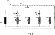
- Fig. 6 shows an impedance model 600 of an RFID transponder of the kind set forth.
- the transponder comprises an integrated circuit 602 and an antenna 604 which are operatively coupled to each other.
- the transmitter impedance 606 i.e. the impedance of the whole integrated circuit
- the transmitter impedance 606 is modeled as the impedance of the modulator 608, the impedance of the LDO regulator 612, the impedance of the voltage limiter 614, and the impedance of other components of the transponder 610 coupled in parallel.
- the switches 616, 618 By closing and opening the switches 616, 618 the transmitter impedance can be controlled.
- the transmitter impedance is increased during a first period of time, by opening the LDO switch 618.
- the transmitter impedance is decreased to a minimum by enabling the modulator (i.e. by closing the modulator switch 616). It is noted that, in the second period, the LDO switch may be closed again or it may remain open. Since the modulator dominates in this second period, closing and opening the LDO switch will have a negligible effect on the impedance.
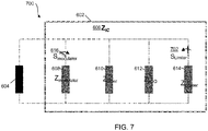
- Fig. 7 shows another impedance model 700 of an RFID transponder of the kind set forth.
- the transponder comprises an integrated circuit 602 and an antenna 604 which are operatively coupled to each other.
- the transmitter impedance 606 i.e. the impedance of the whole integrated circuit
- the transmitter impedance 606 is modeled as the impedance of the modulator 608, the impedance of the LDO regulator 612, the impedance of the voltage limiter 614, and the impedance of other components of the transponder 610 coupled in parallel.
- the transmitter impedance can be controlled.
- the transmitter impedance is increased during a first period of time, by opening the voltage limiter switch 702.
- the transmitter impedance is decreased to a minimum by enabling the modulator (i.e. by closing the modulator switch 616).
Landscapes
- Engineering & Computer Science (AREA)
- Physics & Mathematics (AREA)
- General Physics & Mathematics (AREA)
- Theoretical Computer Science (AREA)
- Computer Networks & Wireless Communication (AREA)
- Computer Hardware Design (AREA)
- Microelectronics & Electronic Packaging (AREA)
- Artificial Intelligence (AREA)
- Computer Vision & Pattern Recognition (AREA)
- Near-Field Transmission Systems (AREA)
Abstract
Description
- The present disclosure relates to a transponder. Furthermore, the present disclosure relates to a corresponding method of operating a transponder.
- Nowadays, radio frequency identification (RFID) transponders are widely used, in different areas of industry and commerce and for various purposes. RFID transponders may for example be embodied as so-called RFID tags or RFID cards. It is noted that, in the present disclosure, near field communication (NFC) transponders are regarded as a specific type of RFID transponders. Thus, the principles described herein may also be applied to NFC transponders.
- In accordance with a first aspect of the present disclosure, a radio frequency identification (RFID) transponder is provided, comprising a modulator and a controller, wherein: the modulator is configured to generate a modulated signal to be transmitted to an external RFID reader; the controller is configured to increase a transmitter impedance during a first period of time; the controller is configured to decrease the transmitter impedance by enabling the modulator during a second period of time.
- In an embodiment, the controller is configured to increase the transmitter impedance by disabling a low-impedance path within the RFID transponder.
- In an embodiment, the controller is configured to increase the transmitter impedance by disabling a low-dropout, LDO, regulator of the RFID transponder.
- In an embodiment, the LDO regulator is disabled by opening a first switch.
- In an embodiment, the controller is configured to increase the transmitter impedance by disabling a voltage limiter of the RFID transponder.
- In an embodiment, the voltage limiter is disabled by opening a second switch.
- In an embodiment, the modulator is enabled by closing a third switch.
- In an embodiment, the controller is configured to repeatedly increase the transmitter impedance.
- In an embodiment, the controller is configured to disable the modulator after the second period of time.
- In an embodiment, the RFID transponder is an RFID tag.
- In accordance with a second aspect of the present disclosure, a method of operating a radio frequency identification (RFID) transponder is conceived, the RFID transponder comprising a modulator and a controller, the method comprising: the modulator generates a modulated signal to be transmitted to an external RFID reader; the controller increases a transmitter impedance during a first period of time; the controller decreases the transmitter impedance by enabling the modulator during a second period of time.
- In an embodiment, the controller repeatedly increases the transmitter impedance.
- In an embodiment, the controller increases the transmitter impedance by disabling a low-impedance path within the RFID transponder.
- In an embodiment, the controller increases the transmitter impedance by disabling a low-dropout, LDO, regulator of the RFID transponder.
- In an embodiment, the controller increases the transmitter impedance by disabling a voltage limiter of the RFID transponder.
- Embodiments will be described in more detail with reference to the appended drawings, in which:
-
Fig. 1 shows an illustrative embodiment of an RFID transponder; -
Fig. 2 shows an illustrative embodiment of a method of operating an RFID transponder; -
Fig. 3 shows an illustrative embodiment of an RFID communication system; -
Fig. 4 shows an example of a controlled modulation; -
Fig. 5 shows an illustrative embodiment of a controlled modulation; -
Fig. 6 shows an impedance model of an RFID transponder; -
Fig. 7 shows another impedance model of an RFID transponder. - Nowadays, radio frequency identification (RFID) transponders are widely used, in different areas of industry and commerce and for various purposes. RFID transponders may for example be embodied as so-called RFID tags or RFID cards. It is noted that, in the present disclosure, near field communication (NFC) transponders are regarded as a specific type of RFID transponders. Thus, the principles described herein may also be applied to NFC transponders.
- RFID communication may be based on inductive coupling. The communication between an RFID reader and an RFID transponder, such as an RFID tag, is often realized by means of load modulation and can be split into a forward link and a return link. More specifically, the RFID reader may transmit commands to the RFID transponder through a forward link, and the RFID transponder may transmit responses to those commands back to the RFID reader through a return link. The RFID transponder contains a modulator, which load modulates a carrier signal. Different types of load modulation exist, for example active load modulation (ALM) and passive load modulation (PLM). In practice, the strength of the return link may be low, which has a negative impact on the communication between the RFID transponder and the RFID reader.
-
Fig. 1 shows an illustrative embodiment of a radio frequency identification (RFID) transponder. TheRFID transponder 100 includes amodulator 102 controlled by acontroller 104. Themodulator 102 is configured to generate a modulated signal to be transmitted to an external RFID reader (not shown). Furthermore, thecontroller 104 is configured to increase a transmitter impedance during a first period of time. It is noted that the increase of the transmitter impedance correlates with a decreased load on the RFID transponder. In addition, thecontroller 104 is configured to decrease the transmitter impedance by enabling themodulator 102 during a second period of time. Thus, during this second period, the load on the RFID transponder is effectively increased. In this way, the load amplitude can be increased, which in turn increases the strength of the return link. - It is noted that an RFID transponder typically comprises an integrated circuit and an antenna coupled to the integrated circuit. As used herein, the term "transmitter impedance" refers to the impedance of the integrated circuit. The impedance of the integrated circuit is formed by the impedance of the various components of the integrated circuit, as will be explained with reference to
Fig. 6 andFig. 7 . Furthermore, it is noted that the feature of increasing the transmitter impedance before decreasing it using the modulator does not need to be used all the time. In other words, the transponder may also be configured to behave like a conventional transponder when the feature is not active. In an embodiment, thecontroller 104 is configured to repeatedly increase the transmitter impedance. For example, the transmitter impedance may be increased each time before the modulator is enabled. -
Fig. 2 shows an illustrative embodiment of amethod 200 of operating a transponder of the kind set forth. Themethod 200 comprises the following steps. At 202, themodulator 102 generates a modulated signal to be transmitted to an external RFID reader. Furthermore, at 204, the controller increases the transponder impedance during a first period of time. During this first period of time, the modulator is not yet enabled. In other words, during the first period of time, the carrier wave generated by the RFID reader is not being modulated by the RFID transponder. Then, at 206, the controller decreases the transmitter impedance by enabling the modulator during a second period of time. Thus, during the second period of time, the carrier wave generated by the RFID reader is being modulated by the RFID transponder. -
Fig. 3 shows an illustrative embodiment of anRFID communication system 300 in which theRFID transponder 100 is used. Thecommunication system 300 comprises anRFID transponder 100 of the kind set forth and anRFID reader 302 which communicate with each other. TheRFID transponder 100 includes themodulator 102 controlled by thecontroller 104. Similarly, theRFID reader 302 includes ademodulator 304 controller by acontroller 306. In operation, theRFID transponder 100 modulates a carrier wave generated by theRFID reader 302, resulting in a modulated signal. To generate the modulated signal, a conventional transponder either increases or decreases the impedance. In practice, the strength of the return link is limited by the voltage drop of the antenna coil (not shown) of theRFID transponder 100. The voltage drop depends on the strength of the field generated by theRFID reader 302. Thus, a low field strength typically results in a low strength of the return link. As mentioned above, the presently disclosed transponder and corresponding method of operating a transponder increase the strength of the return link. -
Fig. 4 shows an example of a controlledmodulation 400. In particular, a conventional controlledmodulation 400 is shown. A modulatedsignal 402 is generated by alternately closing 404 and opening 406 a switch Smodulator. When the switch Smodulator is closed, the modulator is effectively enabled and the transmitter impedance is decreased. This, in turn, results in an increase of the load on the RFID transponder. Then, when the switch Smodulator is opened, the modulator is effectively disabled and the transmitter impedance is increased. This, in turn, results in an decrease of the load on the RFID transponder. The load amplitude A1 is the difference between the maximum load (when the modulator is enabled) and the minimum load (when the modulator is disabled). -
Fig. 5 shows an illustrative embodiment of a controlledmodulation 500. In contrast to the conventional controlled modulation shown inFig. 4 , the controlledmodulation 500 shown inFig. 5 includes a step of increasing the transmitter impedance during a first period of time, before enabling the modulator. In particular, a modulatedsignal 502 is generated by alternately closing 504 and opening 506 a switch Smodulator. When the switch Smodulator is closed, the modulator is effectively enabled and the transmitter impedance is decreased. This, in turn, results in a increase of the load on the RFID transponder. Then, when the switch Smodulator is opened, the modulator is effectively disabled and the transmitter impedance is increased. This, in turn, results in an decrease of the load on the RFID transponder. However, before closing 504 the switch Smodulator for the first time, a switch SLDO is opened. This effectively disables a low-dropout (LDO) regulator of the RFID transponder, which in turn increases the transmitter impedance. By disabling the LDO regulator the transmitter impedance can easily be increased. As shown inFig. 5 , the decreased load achieved by opening the switch SLDO results in a higher maximum load amplitude on the RFID transponder. Thus, the load amplitude A2 is higher than the amplitude A1 achieved by the controlled modulation shown inFig. 4 . The difference between A2 and A1 is referred to as a gain. The increased load amplitude, in turn, increases the strength of the return link. In another implementation, a voltage limiter of the RFID transponder is disabled. This has a similar effect as disabling the LDO regulator, i.e. it increases the transmitter impedance before the modulator is enabled. Thus, in an embodiment, the controller is configured to increase the transmitter impedance by disabling a low-impedance path within the RFID transponder. This embodiment enables practical and effective implementations. For instance, the transmitter impedance can easily be increased by disabling the LDO regulator and/or the voltage limiter of the RFID transponder. This, in turn, can easily be realized by opening switches between those components and an antenna of the RFID transponder. Similarly, the modulator can easily be enabled by closing a switch between the modulator and the antenna, and it can easily be disabled by closing said switch. - In particular, under normal operation the switch SLDO is closed. To increase the load amplitude the RFID transponder decreases the load as a first step, by reducing the consumed energy (i.e., SLDO is opened). This correlates with an increased impedance and amplitude of the RF field. The limitation of this increase is defined by the coil resistance of the transponder or the lowest ohmic parallel path in the system. After some time the transponder increases the load to a minimum by enabling the modulator (i.e., Smodulator is closed). After some time the modulator is disabled (i.e., Smodulator is opened). This again leads the field to increase, due to a decreased load. The increase of the impedance as a first step leads to an increased load amplitude.
-
Fig. 6 shows animpedance model 600 of an RFID transponder of the kind set forth. The transponder comprises anintegrated circuit 602 and anantenna 604 which are operatively coupled to each other. The transmitter impedance 606 (i.e. the impedance of the whole integrated circuit) is modeled as the impedance of themodulator 608, the impedance of theLDO regulator 612, the impedance of thevoltage limiter 614, and the impedance of other components of thetransponder 610 coupled in parallel. By closing and opening theswitches LDO switch 618. Then, in a second period of time, the transmitter impedance is decreased to a minimum by enabling the modulator (i.e. by closing the modulator switch 616). It is noted that, in the second period, the LDO switch may be closed again or it may remain open. Since the modulator dominates in this second period, closing and opening the LDO switch will have a negligible effect on the impedance. -
Fig. 7 shows anotherimpedance model 700 of an RFID transponder of the kind set forth. Again, the transponder comprises anintegrated circuit 602 and anantenna 604 which are operatively coupled to each other. The transmitter impedance 606 (i.e. the impedance of the whole integrated circuit) is modeled as the impedance of themodulator 608, the impedance of theLDO regulator 612, the impedance of thevoltage limiter 614, and the impedance of other components of thetransponder 610 coupled in parallel. By closing and opening theswitches voltage limiter switch 702. Then, in a second period of time, the transmitter impedance is decreased to a minimum by enabling the modulator (i.e. by closing the modulator switch 616). - It is noted that the embodiments above have been described with reference to different subject-matters. In particular, some embodiments may have been described with reference to method-type claims whereas other embodiments may have been described with reference to apparatus-type claims. However, a person skilled in the art will gather from the above that, unless otherwise indicated, in addition to any combination of features belonging to one type of subject-matter also any combination of features relating to different subject-matters, in particular a combination of features of the method-type claims and features of the apparatus-type claims, is considered to be disclosed with this document.
- Furthermore, it is noted that the drawings are schematic. In different drawings, similar or identical elements are provided with the same reference signs. Furthermore, it is noted that in an effort to provide a concise description of the illustrative embodiments, implementation details which fall into the customary practice of the skilled person may not have been described. It should be appreciated that in the development of any such implementation, as in any engineering or design project, numerous implementation-specific decisions must be made in order to achieve the developers' specific goals, such as compliance with system-related and business-related constraints, which may vary from one implementation to another. Moreover, it should be appreciated that such a development effort might be complex and time consuming, but would nevertheless be a routine undertaking of design, fabrication, and manufacture for those of ordinary skill.
- Finally, it is noted that the skilled person will be able to design many alternative embodiments without departing from the scope of the appended claims. In the claims, any reference sign placed between parentheses shall not be construed as limiting the claim. The word "comprise(s)" or "comprising" does not exclude the presence of elements or steps other than those listed in a claim. The word "a" or "an" preceding an element does not exclude the presence of a plurality of such elements. Measures recited in the claims may be implemented by means of hardware comprising several distinct elements and/or by means of a suitably programmed processor. In a device claim enumerating several means, several of these means may be embodied by one and the same item of hardware. The mere fact that certain measures are recited in mutually different dependent claims does not indicate that a combination of these measures cannot be used to advantage.
-
- 100 RFID transponder
- 102 modulator
- 104 controller
- 200 method of operating an RFID transponder
- 202 generating, by a modulator of an RFID transponder, a modulated signal to be transmitted to an external RFID reader
- 204 increasing, by a controller of the RFID transponder, a transmitter impedance during a first period of time
- 206 decreasing, by the controller, the transmitter impedance by enabling the modulator during a second period of time
- 300 RFID communication system
- 302 RFID reader
- 304 demodulator
- 306 controller
- 400 controlled modulation
- 402 modulated signal
- 404 Smodulator is closed
- 406 Smodulator is opened
- 500 controlled modulation
- 502 modulated signal
- 502 SLDO is opened
- 504 Smodulator is closed
- 506 Smodulator is opened
- 600 impedance model
- 602 transponder IC
- 604 antenna
- 606 IC impedance
- 608 modulator impedance
- 610 impedance of other IC components
- 612 LDO impedance
- 614 limiter impedance
- 616 modulator switch
- 618 LDO switch
- 700 impedance model
- 702 limiter switch
Claims (15)
- A radio frequency identification, RFID, transponder, comprising a modulator and a controller, wherein:the modulator is configured to generate a modulated signal to be transmitted to an external RFID reader;the controller is configured to increase a transmitter impedance during a first period of time;the controller is configured to decrease the transmitter impedance by enabling the modulator during a second period of time.
- The RFID transponder of claim 1, wherein the controller is configured to increase the transmitter impedance by disabling a low-impedance path within the RFID transponder.
- The RFID transponder of any preceding claim, wherein the controller is configured to increase the transmitter impedance by disabling a low-dropout, LDO, regulator of the RFID transponder.
- The RFID transponder of claim 3, wherein the LDO regulator is disabled by opening a first switch.
- The RFID transponder of any preceding claim, wherein the controller is configured to increase the transmitter impedance by disabling a voltage limiter of the RFID transponder.
- The RFID transponder of claim 5, wherein the voltage limiter is disabled by opening a second switch.
- The RFID transponder of any preceding claim, wherein the modulator is enabled by closing a third switch.
- The RFID transponder of any preceding claim, wherein the controller is configured to repeatedly increase the transmitter impedance.
- The RFID transponder of any preceding claim, wherein the controller is configured to disable the modulator after the second period of time.
- The RFID transponder of any preceding claim, being an RFID tag.
- A method of operating a radio frequency identification, RFID, transponder, the RFID transponder comprising a modulator and a controller, the method comprising:the modulator generates a modulated signal to be transmitted to an external RFID reader;the controller increases a transmitter impedance during a first period of time;the controller decreases the transmitter impedance by enabling the modulator during a second period of time.
- The method of claim 11, wherein the controller repeatedly increases the transmitter impedance.
- The method of claim 11 or 12, wherein the controller increases the transmitter impedance by disabling a low-impedance path within the RFID transponder.
- The method of any one of claims 11 to 13, wherein the controller increases the transmitter impedance by disabling a low-dropout, LDO, regulator of the RFID transponder.
- The method of any one of claims 11 to 14, wherein the controller increases the transmitter impedance by disabling a voltage limiter of the RFID transponder.
Priority Applications (3)
| Application Number | Priority Date | Filing Date | Title |
|---|---|---|---|
| EP19179550.9A EP3751462B1 (en) | 2019-06-11 | 2019-06-11 | Transponder and corresponding operating method |
| CN202010458392.1A CN112069840B (en) | 2019-06-11 | 2020-05-26 | Transponder and corresponding operation method |
| US16/893,652 US11126906B2 (en) | 2019-06-11 | 2020-06-05 | Transponder and corresponding operating method |
Applications Claiming Priority (1)
| Application Number | Priority Date | Filing Date | Title |
|---|---|---|---|
| EP19179550.9A EP3751462B1 (en) | 2019-06-11 | 2019-06-11 | Transponder and corresponding operating method |
Publications (2)
| Publication Number | Publication Date |
|---|---|
| EP3751462A1 true EP3751462A1 (en) | 2020-12-16 |
| EP3751462B1 EP3751462B1 (en) | 2022-01-05 |
Family
ID=66826842
Family Applications (1)
| Application Number | Title | Priority Date | Filing Date |
|---|---|---|---|
| EP19179550.9A Not-in-force EP3751462B1 (en) | 2019-06-11 | 2019-06-11 | Transponder and corresponding operating method |
Country Status (3)
| Country | Link |
|---|---|
| US (1) | US11126906B2 (en) |
| EP (1) | EP3751462B1 (en) |
| CN (1) | CN112069840B (en) |
Citations (4)
| Publication number | Priority date | Publication date | Assignee | Title |
|---|---|---|---|---|
| US20060220794A1 (en) * | 2005-04-04 | 2006-10-05 | Jeffrey Zhu | Phase modulation for backscatter transponders |
| US20070115098A1 (en) * | 2005-11-18 | 2007-05-24 | Wj Communications, Inc. | Rfid system including tags having low rf scattering mode |
| EP2330538A1 (en) * | 2009-11-30 | 2011-06-08 | Nxp B.V. | Radio frequency transponder |
| EP2431925A1 (en) * | 2010-09-21 | 2012-03-21 | Inside Secure | Method and device for active load modulation by inductive coupling |
Family Cites Families (13)
| Publication number | Priority date | Publication date | Assignee | Title |
|---|---|---|---|---|
| US6054925A (en) * | 1997-08-27 | 2000-04-25 | Data Investments Limited | High impedance transponder with improved backscatter modulator for electronic identification system |
| US6147606A (en) * | 1998-03-26 | 2000-11-14 | Intermec Ip Corp. | Apparatus and method for radio frequency transponder with improved read distance |
| US6356738B1 (en) * | 1999-02-18 | 2002-03-12 | Gary W. Schneider | Method and apparatus for communicating data with a transponder |
| US6737973B2 (en) | 2001-10-15 | 2004-05-18 | 3M Innovative Properties Company | Amplifier modulation |
| US7259676B2 (en) * | 2005-05-31 | 2007-08-21 | Symbol Technologies, Inc. | Mode-diversity RFAID tag and interrogator system and method for identifying an RFAID transponder |
| FR2900752B1 (en) | 2006-05-05 | 2008-10-10 | Inside Contactless Sa | METHOD AND DEVICE FOR DATA TRANSMISSION BY LOAD MODULATION |
| DE102007004843A1 (en) * | 2007-01-31 | 2008-08-07 | Infineon Technologies Ag | Concept for providing a supply voltage and a load modulation in a transponder |
| DE102007028695A1 (en) | 2007-06-21 | 2009-01-02 | Kathrein-Austria Ges.M.B.H. | Method and device for generating an amplitude-modulated signal |
| US8159291B2 (en) | 2007-12-21 | 2012-04-17 | Datamars S.A. | AM (amplitude modulation) demodulation system for RFID reader device |
| CN102982368A (en) * | 2012-11-06 | 2013-03-20 | 王学祥 | Radio frequency identification (RFID) ultrathin metal-resisting electronic tag based on folded dipole |
| EP3145092B1 (en) * | 2015-09-21 | 2019-06-19 | STMicroelectronics International N.V. | Method and transmitter circuit for communication using active load modulation in radio frequency identification systems |
| US10019608B2 (en) * | 2015-12-09 | 2018-07-10 | Nxp B.V. | Method and device for phase calibration with active load modulation |
| EP3232374B1 (en) * | 2016-04-14 | 2019-12-04 | STMicroelectronics International N.V. | Radio-frequency identification transponder and method for sending a radio-frequency identification message |
-
2019
- 2019-06-11 EP EP19179550.9A patent/EP3751462B1/en not_active Not-in-force
-
2020
- 2020-05-26 CN CN202010458392.1A patent/CN112069840B/en active Active
- 2020-06-05 US US16/893,652 patent/US11126906B2/en active Active
Patent Citations (4)
| Publication number | Priority date | Publication date | Assignee | Title |
|---|---|---|---|---|
| US20060220794A1 (en) * | 2005-04-04 | 2006-10-05 | Jeffrey Zhu | Phase modulation for backscatter transponders |
| US20070115098A1 (en) * | 2005-11-18 | 2007-05-24 | Wj Communications, Inc. | Rfid system including tags having low rf scattering mode |
| EP2330538A1 (en) * | 2009-11-30 | 2011-06-08 | Nxp B.V. | Radio frequency transponder |
| EP2431925A1 (en) * | 2010-09-21 | 2012-03-21 | Inside Secure | Method and device for active load modulation by inductive coupling |
Also Published As
| Publication number | Publication date |
|---|---|
| CN112069840B (en) | 2024-07-16 |
| US20200394487A1 (en) | 2020-12-17 |
| EP3751462B1 (en) | 2022-01-05 |
| CN112069840A (en) | 2020-12-11 |
| US11126906B2 (en) | 2021-09-21 |
Similar Documents
| Publication | Publication Date | Title |
|---|---|---|
| US11514255B1 (en) | Fast frequency switching for RFID applications | |
| US8836512B2 (en) | Self tuning RFID | |
| EP2701314B1 (en) | Detection of load-modulated NFC signals | |
| EP3279837A1 (en) | Electronic tamper detection device | |
| US9514336B2 (en) | Method and system for adaptive operation of a power amplifier of a radio frequency identification (RFID) reader device | |
| US11270177B2 (en) | RFID transponder and corresponding operating method | |
| CN111967280B (en) | RFID transponder and method of operating the same | |
| US7714727B2 (en) | RFID antenna design that can selectively enable and disable the antenna | |
| US11126906B2 (en) | Transponder and corresponding operating method | |
| EP3809329B1 (en) | Clock recovery in an rfid transponder | |
| EP3816860B1 (en) | Rfid transponder and method of operating an rfid transponder | |
| US10984301B2 (en) | Method for limiting the level of a modulated signal received by a tag and corresponding limiter | |
| US11875214B2 (en) | RFID transponder having modifiable settings |
Legal Events
| Date | Code | Title | Description |
|---|---|---|---|
| PUAI | Public reference made under article 153(3) epc to a published international application that has entered the european phase |
Free format text: ORIGINAL CODE: 0009012 |
|
| STAA | Information on the status of an ep patent application or granted ep patent |
Free format text: STATUS: THE APPLICATION HAS BEEN PUBLISHED |
|
| AK | Designated contracting states |
Kind code of ref document: A1 Designated state(s): AL AT BE BG CH CY CZ DE DK EE ES FI FR GB GR HR HU IE IS IT LI LT LU LV MC MK MT NL NO PL PT RO RS SE SI SK SM TR |
|
| AX | Request for extension of the european patent |
Extension state: BA ME |
|
| STAA | Information on the status of an ep patent application or granted ep patent |
Free format text: STATUS: REQUEST FOR EXAMINATION WAS MADE |
|
| 17P | Request for examination filed |
Effective date: 20210616 |
|
| RBV | Designated contracting states (corrected) |
Designated state(s): AL AT BE BG CH CY CZ DE DK EE ES FI FR GB GR HR HU IE IS IT LI LT LU LV MC MK MT NL NO PL PT RO RS SE SI SK SM TR |
|
| GRAP | Despatch of communication of intention to grant a patent |
Free format text: ORIGINAL CODE: EPIDOSNIGR1 |
|
| STAA | Information on the status of an ep patent application or granted ep patent |
Free format text: STATUS: GRANT OF PATENT IS INTENDED |
|
| INTG | Intention to grant announced |
Effective date: 20211006 |
|
| RIN1 | Information on inventor provided before grant (corrected) |
Inventor name: PICHLER, THOMAS |
|
| GRAS | Grant fee paid |
Free format text: ORIGINAL CODE: EPIDOSNIGR3 |
|
| GRAA | (expected) grant |
Free format text: ORIGINAL CODE: 0009210 |
|
| STAA | Information on the status of an ep patent application or granted ep patent |
Free format text: STATUS: THE PATENT HAS BEEN GRANTED |
|
| AK | Designated contracting states |
Kind code of ref document: B1 Designated state(s): AL AT BE BG CH CY CZ DE DK EE ES FI FR GB GR HR HU IE IS IT LI LT LU LV MC MK MT NL NO PL PT RO RS SE SI SK SM TR |
|
| REG | Reference to a national code |
Ref country code: GB Ref legal event code: FG4D |
|
| REG | Reference to a national code |
Ref country code: CH Ref legal event code: EP |
|
| REG | Reference to a national code |
Ref country code: AT Ref legal event code: REF Ref document number: 1461220 Country of ref document: AT Kind code of ref document: T Effective date: 20220115 |
|
| REG | Reference to a national code |
Ref country code: DE Ref legal event code: R096 Ref document number: 602019010581 Country of ref document: DE |
|
| REG | Reference to a national code |
Ref country code: IE Ref legal event code: FG4D |
|
| REG | Reference to a national code |
Ref country code: LT Ref legal event code: MG9D |
|
| REG | Reference to a national code |
Ref country code: NL Ref legal event code: MP Effective date: 20220105 |
|
| REG | Reference to a national code |
Ref country code: AT Ref legal event code: MK05 Ref document number: 1461220 Country of ref document: AT Kind code of ref document: T Effective date: 20220105 |
|
| PG25 | Lapsed in a contracting state [announced via postgrant information from national office to epo] |
Ref country code: NL Free format text: LAPSE BECAUSE OF FAILURE TO SUBMIT A TRANSLATION OF THE DESCRIPTION OR TO PAY THE FEE WITHIN THE PRESCRIBED TIME-LIMIT Effective date: 20220105 |
|
| PG25 | Lapsed in a contracting state [announced via postgrant information from national office to epo] |
Ref country code: SE Free format text: LAPSE BECAUSE OF FAILURE TO SUBMIT A TRANSLATION OF THE DESCRIPTION OR TO PAY THE FEE WITHIN THE PRESCRIBED TIME-LIMIT Effective date: 20220105 Ref country code: RS Free format text: LAPSE BECAUSE OF FAILURE TO SUBMIT A TRANSLATION OF THE DESCRIPTION OR TO PAY THE FEE WITHIN THE PRESCRIBED TIME-LIMIT Effective date: 20220105 Ref country code: PT Free format text: LAPSE BECAUSE OF FAILURE TO SUBMIT A TRANSLATION OF THE DESCRIPTION OR TO PAY THE FEE WITHIN THE PRESCRIBED TIME-LIMIT Effective date: 20220505 Ref country code: NO Free format text: LAPSE BECAUSE OF FAILURE TO SUBMIT A TRANSLATION OF THE DESCRIPTION OR TO PAY THE FEE WITHIN THE PRESCRIBED TIME-LIMIT Effective date: 20220405 Ref country code: LT Free format text: LAPSE BECAUSE OF FAILURE TO SUBMIT A TRANSLATION OF THE DESCRIPTION OR TO PAY THE FEE WITHIN THE PRESCRIBED TIME-LIMIT Effective date: 20220105 Ref country code: HR Free format text: LAPSE BECAUSE OF FAILURE TO SUBMIT A TRANSLATION OF THE DESCRIPTION OR TO PAY THE FEE WITHIN THE PRESCRIBED TIME-LIMIT Effective date: 20220105 Ref country code: ES Free format text: LAPSE BECAUSE OF FAILURE TO SUBMIT A TRANSLATION OF THE DESCRIPTION OR TO PAY THE FEE WITHIN THE PRESCRIBED TIME-LIMIT Effective date: 20220105 Ref country code: BG Free format text: LAPSE BECAUSE OF FAILURE TO SUBMIT A TRANSLATION OF THE DESCRIPTION OR TO PAY THE FEE WITHIN THE PRESCRIBED TIME-LIMIT Effective date: 20220405 |
|
| PG25 | Lapsed in a contracting state [announced via postgrant information from national office to epo] |
Ref country code: PL Free format text: LAPSE BECAUSE OF FAILURE TO SUBMIT A TRANSLATION OF THE DESCRIPTION OR TO PAY THE FEE WITHIN THE PRESCRIBED TIME-LIMIT Effective date: 20220105 Ref country code: LV Free format text: LAPSE BECAUSE OF FAILURE TO SUBMIT A TRANSLATION OF THE DESCRIPTION OR TO PAY THE FEE WITHIN THE PRESCRIBED TIME-LIMIT Effective date: 20220105 Ref country code: GR Free format text: LAPSE BECAUSE OF FAILURE TO SUBMIT A TRANSLATION OF THE DESCRIPTION OR TO PAY THE FEE WITHIN THE PRESCRIBED TIME-LIMIT Effective date: 20220406 Ref country code: FI Free format text: LAPSE BECAUSE OF FAILURE TO SUBMIT A TRANSLATION OF THE DESCRIPTION OR TO PAY THE FEE WITHIN THE PRESCRIBED TIME-LIMIT Effective date: 20220105 Ref country code: AT Free format text: LAPSE BECAUSE OF FAILURE TO SUBMIT A TRANSLATION OF THE DESCRIPTION OR TO PAY THE FEE WITHIN THE PRESCRIBED TIME-LIMIT Effective date: 20220105 |
|
| PG25 | Lapsed in a contracting state [announced via postgrant information from national office to epo] |
Ref country code: IS Free format text: LAPSE BECAUSE OF FAILURE TO SUBMIT A TRANSLATION OF THE DESCRIPTION OR TO PAY THE FEE WITHIN THE PRESCRIBED TIME-LIMIT Effective date: 20220505 |
|
| REG | Reference to a national code |
Ref country code: DE Ref legal event code: R097 Ref document number: 602019010581 Country of ref document: DE |
|
| PG25 | Lapsed in a contracting state [announced via postgrant information from national office to epo] |
Ref country code: SM Free format text: LAPSE BECAUSE OF FAILURE TO SUBMIT A TRANSLATION OF THE DESCRIPTION OR TO PAY THE FEE WITHIN THE PRESCRIBED TIME-LIMIT Effective date: 20220105 Ref country code: SK Free format text: LAPSE BECAUSE OF FAILURE TO SUBMIT A TRANSLATION OF THE DESCRIPTION OR TO PAY THE FEE WITHIN THE PRESCRIBED TIME-LIMIT Effective date: 20220105 Ref country code: RO Free format text: LAPSE BECAUSE OF FAILURE TO SUBMIT A TRANSLATION OF THE DESCRIPTION OR TO PAY THE FEE WITHIN THE PRESCRIBED TIME-LIMIT Effective date: 20220105 Ref country code: EE Free format text: LAPSE BECAUSE OF FAILURE TO SUBMIT A TRANSLATION OF THE DESCRIPTION OR TO PAY THE FEE WITHIN THE PRESCRIBED TIME-LIMIT Effective date: 20220105 Ref country code: DK Free format text: LAPSE BECAUSE OF FAILURE TO SUBMIT A TRANSLATION OF THE DESCRIPTION OR TO PAY THE FEE WITHIN THE PRESCRIBED TIME-LIMIT Effective date: 20220105 Ref country code: CZ Free format text: LAPSE BECAUSE OF FAILURE TO SUBMIT A TRANSLATION OF THE DESCRIPTION OR TO PAY THE FEE WITHIN THE PRESCRIBED TIME-LIMIT Effective date: 20220105 |
|
| PLBE | No opposition filed within time limit |
Free format text: ORIGINAL CODE: 0009261 |
|
| STAA | Information on the status of an ep patent application or granted ep patent |
Free format text: STATUS: NO OPPOSITION FILED WITHIN TIME LIMIT |
|
| PG25 | Lapsed in a contracting state [announced via postgrant information from national office to epo] |
Ref country code: AL Free format text: LAPSE BECAUSE OF FAILURE TO SUBMIT A TRANSLATION OF THE DESCRIPTION OR TO PAY THE FEE WITHIN THE PRESCRIBED TIME-LIMIT Effective date: 20220105 |
|
| 26N | No opposition filed |
Effective date: 20221006 |
|
| PG25 | Lapsed in a contracting state [announced via postgrant information from national office to epo] |
Ref country code: MC Free format text: LAPSE BECAUSE OF FAILURE TO SUBMIT A TRANSLATION OF THE DESCRIPTION OR TO PAY THE FEE WITHIN THE PRESCRIBED TIME-LIMIT Effective date: 20220105 |
|
| REG | Reference to a national code |
Ref country code: CH Ref legal event code: PL |
|
| REG | Reference to a national code |
Ref country code: BE Ref legal event code: MM Effective date: 20220630 |
|
| PG25 | Lapsed in a contracting state [announced via postgrant information from national office to epo] |
Ref country code: SI Free format text: LAPSE BECAUSE OF FAILURE TO SUBMIT A TRANSLATION OF THE DESCRIPTION OR TO PAY THE FEE WITHIN THE PRESCRIBED TIME-LIMIT Effective date: 20220105 |
|
| PG25 | Lapsed in a contracting state [announced via postgrant information from national office to epo] |
Ref country code: LU Free format text: LAPSE BECAUSE OF NON-PAYMENT OF DUE FEES Effective date: 20220611 Ref country code: LI Free format text: LAPSE BECAUSE OF NON-PAYMENT OF DUE FEES Effective date: 20220630 Ref country code: IE Free format text: LAPSE BECAUSE OF NON-PAYMENT OF DUE FEES Effective date: 20220611 Ref country code: CH Free format text: LAPSE BECAUSE OF NON-PAYMENT OF DUE FEES Effective date: 20220630 |
|
| PG25 | Lapsed in a contracting state [announced via postgrant information from national office to epo] |
Ref country code: BE Free format text: LAPSE BECAUSE OF NON-PAYMENT OF DUE FEES Effective date: 20220630 |
|
| PG25 | Lapsed in a contracting state [announced via postgrant information from national office to epo] |
Ref country code: IT Free format text: LAPSE BECAUSE OF FAILURE TO SUBMIT A TRANSLATION OF THE DESCRIPTION OR TO PAY THE FEE WITHIN THE PRESCRIBED TIME-LIMIT Effective date: 20220105 |
|
| P01 | Opt-out of the competence of the unified patent court (upc) registered |
Effective date: 20230725 |
|
| GBPC | Gb: european patent ceased through non-payment of renewal fee |
Effective date: 20230611 |
|
| PG25 | Lapsed in a contracting state [announced via postgrant information from national office to epo] |
Ref country code: MK Free format text: LAPSE BECAUSE OF FAILURE TO SUBMIT A TRANSLATION OF THE DESCRIPTION OR TO PAY THE FEE WITHIN THE PRESCRIBED TIME-LIMIT Effective date: 20220105 Ref country code: CY Free format text: LAPSE BECAUSE OF FAILURE TO SUBMIT A TRANSLATION OF THE DESCRIPTION OR TO PAY THE FEE WITHIN THE PRESCRIBED TIME-LIMIT Effective date: 20220105 Ref country code: GB Free format text: LAPSE BECAUSE OF NON-PAYMENT OF DUE FEES Effective date: 20230611 |
|
| PG25 | Lapsed in a contracting state [announced via postgrant information from national office to epo] |
Ref country code: HU Free format text: LAPSE BECAUSE OF FAILURE TO SUBMIT A TRANSLATION OF THE DESCRIPTION OR TO PAY THE FEE WITHIN THE PRESCRIBED TIME-LIMIT; INVALID AB INITIO Effective date: 20190611 |
|
| PG25 | Lapsed in a contracting state [announced via postgrant information from national office to epo] |
Ref country code: TR Free format text: LAPSE BECAUSE OF FAILURE TO SUBMIT A TRANSLATION OF THE DESCRIPTION OR TO PAY THE FEE WITHIN THE PRESCRIBED TIME-LIMIT Effective date: 20220105 |
|
| PGFP | Annual fee paid to national office [announced via postgrant information from national office to epo] |
Ref country code: DE Payment date: 20240521 Year of fee payment: 6 |
|
| PGFP | Annual fee paid to national office [announced via postgrant information from national office to epo] |
Ref country code: FR Payment date: 20240522 Year of fee payment: 6 |
|
| PG25 | Lapsed in a contracting state [announced via postgrant information from national office to epo] |
Ref country code: MT Free format text: LAPSE BECAUSE OF FAILURE TO SUBMIT A TRANSLATION OF THE DESCRIPTION OR TO PAY THE FEE WITHIN THE PRESCRIBED TIME-LIMIT Effective date: 20220105 |
|
| REG | Reference to a national code |
Ref country code: DE Ref legal event code: R119 Ref document number: 602019010581 Country of ref document: DE |
|
| PG25 | Lapsed in a contracting state [announced via postgrant information from national office to epo] |
Ref country code: DE Free format text: LAPSE BECAUSE OF NON-PAYMENT OF DUE FEES Effective date: 20260101 |
|
| PG25 | Lapsed in a contracting state [announced via postgrant information from national office to epo] |
Ref country code: FR Free format text: LAPSE BECAUSE OF NON-PAYMENT OF DUE FEES Effective date: 20250630 |