EP3748694A1 - Solar cell design that minimizes weld attrition and gridline shadowing losses - Google Patents
Solar cell design that minimizes weld attrition and gridline shadowing losses Download PDFInfo
- Publication number
- EP3748694A1 EP3748694A1 EP20177750.5A EP20177750A EP3748694A1 EP 3748694 A1 EP3748694 A1 EP 3748694A1 EP 20177750 A EP20177750 A EP 20177750A EP 3748694 A1 EP3748694 A1 EP 3748694A1
- Authority
- EP
- European Patent Office
- Prior art keywords
- metal grid
- cap layer
- width
- cap
- solar cell
- Prior art date
- Legal status (The legal status is an assumption and is not a legal conclusion. Google has not performed a legal analysis and makes no representation as to the accuracy of the status listed.)
- Granted
Links
Images




Classifications
-
- H—ELECTRICITY
- H10—SEMICONDUCTOR DEVICES; ELECTRIC SOLID-STATE DEVICES NOT OTHERWISE PROVIDED FOR
- H10F—INORGANIC SEMICONDUCTOR DEVICES SENSITIVE TO INFRARED RADIATION, LIGHT, ELECTROMAGNETIC RADIATION OF SHORTER WAVELENGTH OR CORPUSCULAR RADIATION
- H10F77/00—Constructional details of devices covered by this subclass
- H10F77/20—Electrodes
- H10F77/206—Electrodes for devices having potential barriers
- H10F77/211—Electrodes for devices having potential barriers for photovoltaic cells
- H10F77/215—Geometries of grid contacts
-
- H—ELECTRICITY
- H10—SEMICONDUCTOR DEVICES; ELECTRIC SOLID-STATE DEVICES NOT OTHERWISE PROVIDED FOR
- H10F—INORGANIC SEMICONDUCTOR DEVICES SENSITIVE TO INFRARED RADIATION, LIGHT, ELECTROMAGNETIC RADIATION OF SHORTER WAVELENGTH OR CORPUSCULAR RADIATION
- H10F71/00—Manufacture or treatment of devices covered by this subclass
-
- Y—GENERAL TAGGING OF NEW TECHNOLOGICAL DEVELOPMENTS; GENERAL TAGGING OF CROSS-SECTIONAL TECHNOLOGIES SPANNING OVER SEVERAL SECTIONS OF THE IPC; TECHNICAL SUBJECTS COVERED BY FORMER USPC CROSS-REFERENCE ART COLLECTIONS [XRACs] AND DIGESTS
- Y02—TECHNOLOGIES OR APPLICATIONS FOR MITIGATION OR ADAPTATION AGAINST CLIMATE CHANGE
- Y02E—REDUCTION OF GREENHOUSE GAS [GHG] EMISSIONS, RELATED TO ENERGY GENERATION, TRANSMISSION OR DISTRIBUTION
- Y02E10/00—Energy generation through renewable energy sources
- Y02E10/50—Photovoltaic [PV] energy
Definitions
- This disclosure is related generally to a solar cell design that minimizes weld attrition and gridline shadowing losses.
- a welding process is used to connect space solar cells in series.
- Traditional space solar cells are connected in series with an interconnect welded to the front of one cell and the back side of an adjacent cell.
- the welding process on the backside of the cell in particular requires high localized pressures and temperatures.
- Gridlines are comprised of at least two layers including a metal grid and a semiconductor cap layer. A stress concentration factor exists for each layer.
- the alignment of the metal grid relative to the cap layer, and the width of the cap layer relative to the width of the metal grid, are controlled at areas on the front surface of the solar cell opposite where welding occurs on a back-side of the solar cell.
- the alignment of the metal grid relative to the cap layer, and the width of the cap layer relative to the width of the metal grid, are controlled by a photomask.
- the device as fabricated comprises: a solar cell including one or more gridlines for extracting photo-current on a front surface of the solar cell, wherein: each of the gridlines is a metal grid and a cap layer, and at least a portion of the metal grid is deposited on the cap layer; and an alignment of the metal grid relative to the cap layer and a width of the cap layer relative to a width of the metal grid are controlled so that a minimum cap edge offset distance value is 1 ⁇ m or more or about 1 ⁇ m or more.
- the width 106B of the cap layer 105 relative to the width 106A of the metal grid 104 can be independently controlled at any spatial location on the solar cell 100 via the design of independent photomasks for the metal grid 104 and cap layer 105.
- the width 106B of the cap layer 105 is equal the width 106A of the metal grid 104 to minimize unwanted shadowing of the solar cell 100.
- Both the metal grid 104 and cap layer 105 are absorptive and prevent current generation where they exist on the front surface of the solar cell 100.
- FIG. 4 is a schematic of a photomask 400 of a back-side of a solar cell 100 indicating areas of modification to the grids 104 and cap layers 105 on the front-side of the solar cell 100 to minimize weld attrition.
- the cap layers 105 are 10 ⁇ m or about 10 ⁇ m wider than the metal grids 104 only in areas opposite where the welding occurs on the back-side of the solar cell 100. In this way, attrition is minimized as the areas where the weld occurs has Minimum Cap Edge Offset Distance values of 5 ⁇ m or about 5 ⁇ m in a perfect alignment case.
- Block 502 represents the step of controlling an alignment of the metal grid 104 relative to the cap layer 105 and a width of the cap layer 105 relative to a width of the metal grid 104 so that a Minimum Cap Edge Offset Distance value is 1 ⁇ m or more or about 1 ⁇ m or more.
- Cap Edge Offset L and Cap Edge Offset R values 107A, 107B representing distances of edges of the cap layer 105 from the edges of the metal grid 104 on a left and right side of the cap layer 105, respectively
- the Minimum Cap Edge Offset Distance value is a minimum value between the Cap Edge Offset L and Cap Edge Offset R values 107A, 107B.
- the Minimum Cap Edge Offset Distance value preferably is 5% to 25% or about 5% to 25% of the width 106A of the metal grid 104.
- a system integrator may include without limitation any number of manufacturers and major-system subcontractors; a third party may include without limitation any number of venders, subcontractors, and suppliers; and an operator may be a satellite company, military entity, service organization, and so on.
- At least one of the solar cells 100 includes one or more gridlines 103 for extracting photo-current on a front surface of the solar cell 100, wherein each of the gridlines 103 is a metal grid 104 and a cap layer 105, and at least a portion of the metal grid 104 is deposited on the cap layer 105.
- An alignment of the metal grid 104 relative to the cap layer 105 and a width of the cap layer 105 relative to a width of the metal grid 104 are controlled so that a Minimum Cap Edge Offset Distance value is 1 ⁇ m or more or about 1 ⁇ m or more.
- Cap Edge Offset L and Cap Edge Offset R values 107A, 107B representing distances of edges of the cap layer 105 from edges of the metal grid 104 on a left and right side of the cap layer 105, respectively
- the Minimum Cap Edge Offset Distance value is a minimum value between the Cap Edge Offset L and Cap Edge Offset R values 107A, 107B.
- the Minimum Cap Edge Offset Distance value preferably is 5% to 25% or about 5% to 25% of the width 106A of the metal grid 104.
- the alignment of the metal grid 104 relative to the cap layer 105, and the width 106A of the metal grid 104 relative to the width 106B of the cap layer 105, are controlled by a photomask 400.
- the width 106B of the cap layer 105 may be less than the width 106A of the metal grid 104 or the width 106B of the cap layer 105 may be greater than the width 106A of the metal grid 104.
Landscapes
- Photovoltaic Devices (AREA)
- Engineering & Computer Science (AREA)
- Manufacturing & Machinery (AREA)
Abstract
Description
- This disclosure is related generally to a solar cell design that minimizes weld attrition and gridline shadowing losses.
- A welding process is used to connect space solar cells in series. Traditional space solar cells are connected in series with an interconnect welded to the front of one cell and the back side of an adjacent cell. The welding process on the backside of the cell in particular requires high localized pressures and temperatures.
- However, the high localized pressures and temperatures from the welding process can crack the solar cell, leading to high rejection rates for the solar cells. Front side features on the solar cells, such as metal gridlines, create stress concentration points which lead to an increase in the rate of crack generation for the solar cell during the welding process.
- Stress concentration factors occur at any change in geometry of the solar cell. For example, gridlines are comprised of at least two layers including a metal grid and a semiconductor cap layer. A stress concentration factor exists for each layer.
- Designing the edges of the cap layer and metal grid in close proximity maximizes cell efficiency, but also multiplies the two stress concentration factors, increasing the likelihood of cracks. Gridlines must be distributed uniformly across the front surface to extract power efficiently, so there is no practical way to avoid backside welding at the same location as front-side gridlines.
- Changes to the welding process parameters have been used to mitigate attrition in the past. The parameters include modifying fixture temperatures, weld force, weld pulse shapes, counts or duration, or changing the shape or size of weld tips.
- Nonetheless, there is a need for improved solar cell designs that mitigate attrition in the welding process.
- To overcome the limitations described above, and to overcome other limitations that will become apparent upon reading and understanding the present specification, this disclosure describes a method of fabricating a device, and the device as fabricated, wherein the device comprises a solar cell design that minimizes weld attrition and gridline shadowing losses.
- The method comprises: fabricating one or more gridlines for extracting photo-current on a front surface of a solar cell, wherein each of the gridlines is a metal grid and a cap layer, and at least a portion of the metal grid is deposited on the cap layer; and controlling an alignment of the metal grid relative to the cap layer and a width of the cap layer relative to a width of the metal grid so that a minimum cap edge offset distance value is 1 µm or more or about 1 µm or more.
- Controlling the alignment of the metal grid relative to the cap layer and the width of the cap layer relative to the width of the metal grid results in cap edge offset L and cap edge offset R values representing distances of edges of the cap layer from edges of the metal grid on a left and right side of the cap layer, respectively, and the minimum cap edge offset distance value is a minimum value between the cap edge offset L and cap edge offset R values. The minimum cap edge offset distance value is 5% to 25% or about 5% to 25% of the width of the metal grid.
- The alignment of the metal grid relative to the cap layer, and the width of the cap layer relative to the width of the metal grid, are controlled at areas on the front surface of the solar cell opposite where welding occurs on a back-side of the solar cell. The alignment of the metal grid relative to the cap layer, and the width of the cap layer relative to the width of the metal grid, are controlled by a photomask.
- An edge of the metal grid and an edge of the cap layer are separated far enough apart that stress concentration factors do not interact, in order to reduce cracks on a back-side of the solar cell that result from welding, without impacting the solar cell's efficiency. Preferably, the edge of the metal grid and the edge of the cap layer are separated by a distance of at least 1 µm.
- The device as fabricated comprises: a solar cell including one or more gridlines for extracting photo-current on a front surface of the solar cell, wherein: each of the gridlines is a metal grid and a cap layer, and at least a portion of the metal grid is deposited on the cap layer; and an alignment of the metal grid relative to the cap layer and a width of the cap layer relative to a width of the metal grid are controlled so that a minimum cap edge offset distance value is 1 µm or more or about 1 µm or more.
- Referring now to the drawings in which like reference numbers represent corresponding parts throughout:
-
FIG. 1 is a schematic of a solar cell showing a cross-section thereof. -
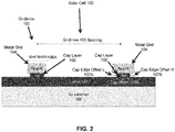
FIG. 2 is a schematic of a solar cell showing a cross-section thereof. -
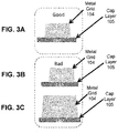
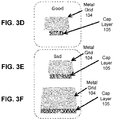
FIGS. 3A, 3B, 3C ,3D, 3E and 3F are schematics of a metal grid and cap layer corresponding toFIGS. 1 and2 , each showing a cross-section thereof. -
FIG. 4 is a schematic of a photomask of solar cells indicating the areas altered to minimize weld attrition. -
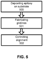
FIG. 5 is a flowchart illustrating a method for fabricating a solar cell. -
FIG. 6A illustrates a method of fabricating a solar cell, solar cell panel and/or satellite. -
FIG. 6B illustrates a resulting satellite having a solar cell panel comprised of solar cells. -
FIG. 7 is an illustration of the solar cell panel in the form of a functional block diagram. - In the following description, reference is made to the accompanying drawings which form a part hereof, and in which is shown by way of illustration a specific example in which the disclosure may be practiced. It is to be understood that other examples may be utilized and structural changes may be made without departing from the scope of the present disclosure.
- Traditional space solar cells are connected in series with an interconnect welded to the front of one cell and the back side of an adjacent cell. The welding process on the backside of the cell in particular requires high localized pressures and temperatures that can lead to cracks in the solar cells, leading to, in some examples, attrition levels exceeding 20% at a potential cost of 1-4 million dollars, depending on production volumes.
- A root cause and corrective action (RCCA) investigation found that subtle changes in the gridlines configuration on the front surface of the solar cell can greatly increase the rate of cracks due to welding on the back-side of the solar cell. This disclosure modifies the design of the gridlines to reduce cracks from back-side welding without significant tradeoffs to the solar cell efficiency. Specifically, this disclosure ensures that metal grid and cap layer edges are separated far enough apart that the stress concentration factors do not interact, reducing cracks from back-side welding without impacting the solar cell efficiency. From a mask design perspective, sharp alignment of the cap layer and metal grid has also been mitigated by designing the cap layer wider than the metal grid in what is known as a "cap greater than metal" (CGM) alignment.
-
FIGS. 1 and2 are schematics of devices, wherein both devices comprise asolar cell 100, showing a cross-section thereof, including a profile view of thesolar cell 100, and describing a method of fabricating the devices. - The
solar cell 100 is comprised of a germanium (Ge)substrate 101 andsemiconductor epitaxy 102, with one or moreperiodic gridlines 103 on a front surface of thesolar cell 100. Each of thegridlines 103 is ametal grid 104 comprised of silver (Ag) and anabsorptive cap layer 105 comprised of gallium arsenide (GaAs), wherein at least a portion of themetal grid 104 is deposited on thecap layer 105. - The
gridlines 103 extract photo-current out of the front surface of thesolar cell 100. Thecap layer 105 is needed to make ohmic contact between themetal grid 104 and thesemiconductor epitaxy 102. Themetal grid 104 carries the current to an ohmic pad for power extraction off thesolar cell 100. -
FIG. 1 illustrates an example where thewidth 106A of themetal grid 104 is narrower than the width 106b of thecap layer 105, whileFIG. 2 illustrates an example where thewidth 106A of themetal grid 104 is wider than thewidth 106B of thecap layer 105. - Depending on the alignment of the
metal grid 104 to thecap layer 105, and therelative widths metal grid 104 andcap layer 105, there are Cap Edge Offset L and Cap EdgeOffset R values cap layer 105 from edges of themetal grid 104 on a left and right side of thecap layer 105, respectively. A Minimum Cap Edge Offset Distance value is a minimum value between the Cap Edge Offset L and Cap EdgeOffset R values relative widths - Over the course of the RCCA investigation, it was determined that back-side weld attrition has a dramatic dependence on the Minimum Cap Edge Offset Distance value. Specifically, there is a rapid onset of transition into attrition starting at a Minimum Cap Edge Offset Distance value of less than 1 µm.
- For Minimum Cap Edge Offset Distance values over 1 µm, the backside weld attrition is near 0. For Minimum Cap Edge Offset Distance values < 1 µm, there is an increase in attrition to 15-20% losses per weld. As all
solar cells 100 in the factory have at least two welds, total losses can approach 50% in the factory from a single process step. - An analysis was performed to better understand the mechanism behind the clear dependence between weld attrition and the Minimum Cap Edge Offset Distance values. The analysis confirms that stress associated with the weld is concentrated at the edge of the
cap layer 105 to the epitaxy layers 102. That stress is enhanced by nearly a factor of 2 when the edge of themetal grid 104 is aligned to the edge of thecap layer 105, or when the Minimum Cap Edge Offset Distance value approaches 0. - This disclosure reduces the gridline stress concentration that leads to the large weld attrition numbers. In the
solar cell 100 fabrication process, thewidth 106B of thecap layer 105 relative to thewidth 106A of themetal grid 104 can be independently controlled at any spatial location on thesolar cell 100 via the design of independent photomasks for themetal grid 104 andcap layer 105. - Typically, a choice is made to engineer the
width 106B of thecap layer 105 to be equal thewidth 106A of themetal grid 104 to minimize unwanted shadowing of thesolar cell 100. Both themetal grid 104 andcap layer 105 are absorptive and prevent current generation where they exist on the front surface of thesolar cell 100. - Unfortunately, if the
width 106B of thecap layer 105 and thewidth 106A of themetal grid 104 are equal, this, by definition, would result in a Minimum Cap Edge Offset Distance value of near 0, resulting in unacceptable levels of attrition. Engineering thewidth 106B of thecap layer 105 relative to thewidth 106A of themetal grid 104 to result in a large Minimum Cap Edge Offset Distance value would solve the attrition issue, but lead to unacceptable levels of shadowing loss andsolar cell 100 performance. -
FIGS. 3A, 3B and 3C are schematics of themetal grid 104 andcap layer 105 corresponding toFIG. 1 , each showing a cross-section thereof, where thewidth 106A of themetal grid 104 is narrower than the width 106b of thecap layer 105, and indicating that the alignment ofFIG. 3A provides good results, while the alignments ofFIGS. 3B and 3C provide bad results. - Similarly,
FIGS. 3D, 3E and 3F are schematics of themetal grid 104 andcap layer 105 corresponding toFIG. 2 , each showing a cross-section thereof, where thewidth 106A of themetal grid 104 is wider than the width 106b of thecap layer 105, and indicating that the alignment ofFIG. 3D provides good results, while the alignments ofFIGS. 3E and 3F provide bad results. -
FIG. 4 is a schematic of aphotomask 400 of a back-side of asolar cell 100 indicating areas of modification to thegrids 104 and cap layers 105 on the front-side of thesolar cell 100 to minimize weld attrition. Specifically, the cap layers 105 are 10 µm or about 10 µm wider than themetal grids 104 only in areas opposite where the welding occurs on the back-side of thesolar cell 100. In this way, attrition is minimized as the areas where the weld occurs has Minimum Cap Edge Offset Distance values of 5 µm or about 5 µm in a perfect alignment case. - This provides a margin in the case where the
widths 106B of the cap layers 105, thewidths 106A of themetal grids 104, and the alignment, varies over the course of production. Moreover, the impact on the efficiency is minimal as the increase in thewidths 106B of the cap layers 105 occurs only a small fractional area of thesolar cell 100. Calculations put the impact on thesolar cell 100 current on a 0.01% level. - In an
alternative photomask 400, the cap layers 105 are 10 µm or about 10 µm narrower than themetal grids 104 only in areas opposite where the welding occurs on the back-side of thesolar cell 100. Again, attrition is minimized as the areas where the weld occurs has Minimum Cap Edge Offset Distance values of 5 µm or about 5 µm in a perfect alignment case. -
FIG. 5 is a flowchart illustrating a method for fabricating thesolar cell 100, according to one example. -
Block 500 represents the step of depositing thesemiconductor epitaxy 102 on theGe substrate 101, thereby forming thesolar cell 100. -
Block 501 represents the step of fabricating one ormore gridlines 103 for extracting photo-current on a front surface of thesolar cell 100, wherein each of thegridlines 103 is ametal grid 104 and acap layer 105, and at least a portion of themetal grid 104 is deposited on thecap layer 105. -
Block 502 represents the step of controlling an alignment of themetal grid 104 relative to thecap layer 105 and a width of thecap layer 105 relative to a width of themetal grid 104 so that a Minimum Cap Edge Offset Distance value is 1 µm or more or about 1 µm or more. - Controlling the alignment of the
metal grid 104 relative to thecap layer 105 and the width of thecap layer 105 relative to the width of themetal grid 104 results in Cap Edge Offset L and Cap Edge Offset R values 107A, 107B representing distances of edges of thecap layer 105 from the edges of themetal grid 104 on a left and right side of thecap layer 105, respectively, and the Minimum Cap Edge Offset Distance value is a minimum value between the Cap Edge Offset L and Cap Edge Offset R values 107A, 107B. The Minimum Cap Edge Offset Distance value preferably is 5% to 25% or about 5% to 25% of thewidth 106A of themetal grid 104. - The alignment of the
metal grid 104 relative to thecap layer 105 and the width of thecap layer 105 relative to the width of themetal grid 104 are controlled at areas on the front surface of thesolar cell 100 opposite where welding occurs on a back-side of thesolar cell 100. - An edge of the
metal grid 104 and an edge of thecap layer 105 are separated far enough apart that stress concentration factors do not interact, in order to reduce cracks on a back-side of thesolar cell 100 that result from the welding, without impacting the solar cell's 100 efficiency. The edge of themetal grid 104 and the edge of thecap layer 105 are separated by a distance of at least 1 µm, at least 1.5 to 2 µm, or at least 3 to 100 µm or more. - The alignment of the
metal grid 104 relative to thecap layer 105, and thewidth 106B of thecap layer 105 relative to thewidth 106A of themetal grid 104, are controlled by aphotomask 400. Thewidth 106B of thecap layer 105 may be less than thewidth 106A of themetal grid 104 or thewidth 106B of thecap layer 105 may be greater than thewidth 106A of themetal grid 104. - Previous to this disclosure, solutions for solar cell cracks at gridlines from back-side welding were limited to changing weld conditions or to having a wider cap layer relative to the metal grid over the entire solar cell area.
- Changes to the welding process can result in lower solar cell attrition. However, this typically results in welding conditions that reduce the strength of the weld joint. In the extreme thermal environments space solar cells experience in mission, loss of weld strength can result in failures of the weld joints. These failures would impact performance of the solar cell array during the mission. This disclosure requires no changes to the weld process and therefore no loss of weld reliability.
- The disclosure is also superior to a solution that has the cap layer wider than the metal grid ("cap greater than metal" or CGM) over the entire solar cell area. A cap greater than metal solution leads to unnecessary reductions in solar cell current on the order of 1% relative. What is proposed here is to use the photomask design to widen the cap layer in only critical welding areas. In this way, with "cap equal to metal" (CEM) over the vast majority of the solar cell area, thereby minimizing the effects on current collection, but at the same time ensuring a Minimum Cap Edge Offset Distance value >> 1 µm in the areas where the welds occur. Effectively, this disclosure provides a method to minimize both attrition and shadowing losses.
- The description set forth above has been presented for purposes of illustration and description, and is not intended to be exhaustive or limited to the examples described. Many alternatives and modifications may be used in place of the specific description set forth above.
- For example, although this disclosure describes the use of gridlines for solar cells, it could be broadened to cover any pattern of metallization used to collect current on a surface of a solar cell.
- In other examples, although the metal grid is described as comprising Ag and the cap layer is described as comprising GaAs, other materials could also be used.
- In yet other examples, although this disclosure describes the Minimum Cap Edge Offset Distance value as 1 µm or more or about 1 µm or more, the Minimum Cap Edge Offset Distance value may be at least 1.5 to 2 µm, or 3 to 100 µm or more.
- Similarly, although this disclosure describes the edge of the metal grid and the edge of the cap layer as being separated by a distance of at least 1 µm, the distance may be at least 1.5 to 2 µm, or 3 to 100 µm or more.
- Examples of the disclosure may be described in the context of a
method 600 of fabricating a solar cell, solar cell panel and/or aerospace vehicle such as a satellite, comprising steps 602-614, as shown inFIG. 6A , wherein the resultingsatellite 616 comprised ofvarious systems 618 and abody 620, including apanel 622 comprised of anarray 624 of one or moresolar cells 100 is shown inFIG. 6B . - As illustrated in
FIG. 6A , during pre-production,exemplary method 600 may include specification anddesign 602 of thesatellite 616, andmaterial procurement 604 for same. During production, component andsubassembly manufacturing 606 andsystem integration 608 of thesatellite 616 takes place, which include fabricating thesatellite 616,panel 622,array 624 andsolar cells 100. Thereafter, thesatellite 616 may go through certification anddelivery 610 in order to be placed inservice 612. Thesatellite 616 may also be scheduled for maintenance and service 614 (which includes modification, reconfiguration, refurbishment, and so on), before being launched. - Each of the processes of
method 600 may be performed or carried out by a system integrator, a third party, and/or an operator (e.g., a customer). For the purposes of this description, a system integrator may include without limitation any number of manufacturers and major-system subcontractors; a third party may include without limitation any number of venders, subcontractors, and suppliers; and an operator may be a satellite company, military entity, service organization, and so on. - As shown in
FIG. 6B , thesatellite 616 fabricated byexemplary method 600 may includevarious systems 618 and abody 620. Examples of thesystems 618 included with thesatellite 616 include, but are not limited to, one or more of apropulsion system 626, anelectrical system 628, acommunications system 630, and apower system 632. Any number of other systems also may be included. -
FIG. 7 is an illustration of thepanel 622 in the form of a functional block diagram, according to one example. Thepanel 622 is comprised of thearray 624, which is comprised of one or more of thesolar cells 100 individually attached to thepanel 622. Each of thesolar cells 100 absorbs light 700 from a light source 702 and generates an electrical output 704 in response thereto. - At least one of the
solar cells 100 includes one ormore gridlines 103 for extracting photo-current on a front surface of thesolar cell 100, wherein each of thegridlines 103 is ametal grid 104 and acap layer 105, and at least a portion of themetal grid 104 is deposited on thecap layer 105. An alignment of themetal grid 104 relative to thecap layer 105 and a width of thecap layer 105 relative to a width of themetal grid 104 are controlled so that a Minimum Cap Edge Offset Distance value is 1 µm or more or about 1 µm or more. - The alignment of the
metal grid 104 relative to thecap layer 105 and the width of thecap layer 105 relative to the width of themetal grid 104 result in Cap Edge Offset L and Cap Edge Offset R values 107A, 107B representing distances of edges of thecap layer 105 from edges of themetal grid 104 on a left and right side of thecap layer 105, respectively, and the Minimum Cap Edge Offset Distance value is a minimum value between the Cap Edge Offset L and Cap Edge Offset R values 107A, 107B. The Minimum Cap Edge Offset Distance value preferably is 5% to 25% or about 5% to 25% of thewidth 106A of themetal grid 104. - The alignment of the
metal grid 104 relative to thecap layer 105 and the width of thecap layer 105 relative to the width of themetal grid 104 are controlled at areas on the front surface of thesolar cell 100 opposite where welding occurs on a back-side of thesolar cell 100. - An edge of the
metal grid 104 and an edge of thecap layer 105 are separated far enough apart that stress concentration factors do not interact, in order to reduce cracks on a back-side of thesolar cell 100 that result from the welding, without impacting the solar cell's 100 efficiency. The edge of themetal grid 104 and the edge of thecap layer 105 are separated by a distance of at least 1 µm, at least 1.5 to 2 µm, or at least 3 to 100 µm or more. - The alignment of the
metal grid 104 relative to thecap layer 105, and thewidth 106A of themetal grid 104 relative to thewidth 106B of thecap layer 105, are controlled by aphotomask 400. Thewidth 106B of thecap layer 105 may be less than thewidth 106A of themetal grid 104 or thewidth 106B of thecap layer 105 may be greater than thewidth 106A of themetal grid 104. - Further, the disclosure comprises examples according to the following clauses:
- Clause 1. A method, comprising: fabricating one or more gridlines for extracting photo-current on a front surface of a solar cell, wherein each of the gridlines is a metal grid and a cap layer, and at least a portion of the metal grid is deposited on the cap layer; and controlling an alignment of the metal grid relative to the cap layer and a width of the cap layer relative to a width of the metal grid so that a minimum cap edge offset distance value is 1 µm or more (or about 1 µm or more).
- Clause 2. The method of Clause 1, wherein controlling the alignment of the metal grid relative to the cap layer and the width of the cap layer relative to the width of the metal grid results in cap edge offset L and cap edge offset R values representing distances of edges of the cap layer from edges of the metal grid on a left and right side of the cap layer, respectively, and the minimum cap edge offset distance value is a minimum value between the cap edge offset L and cap edge offset R values.
- Clause 3. The method of Clause 2, wherein the minimum cap edge offset distance value is 5% to 25% (or about 5% to 25%) of the width of the metal grid.
- Clause 4. The method of any of Clauses 1-3, wherein the alignment of the metal grid relative to the cap layer and the width of the cap layer relative to the width of the metal grid are controlled at areas on the front surface of the solar cell opposite where welding occurs on a back-side of the solar cell.
- Clause 5. The method of Clause 4, wherein an edge of the metal grid and an edge of the cap layer are separated far enough apart that stress concentration factors do not interact, in order to reduce cracks on the back-side of the solar cell that result from the welding, without impacting the solar cell's efficiency.
- Clause 6. The method of Clause 5, wherein the edge of the metal grid and the edge of the cap layer are separated by a distance of at least 1 µm.
- Clause 7. The method of Clause 6, wherein the edge of the metal grid and the edge of the cap layer are separated by a distance of 1.5 µm to 2 µm (or at least 1.5 to 2 µm).
- Clause 8. The method of Clause 7, wherein the edge of the metal grid and the edge of the cap layer are separated by a distance of 3 µm to 100 µm or more (or at least 3 to 100 µm or more).
- Clause 9. The method of any of Clauses 1-8, wherein the alignment of the metal grid relative to the cap layer is controlled by a photomask.
- Clause 10. The method of Clause 9, wherein the width of the cap layer relative to the width of the metal grid is controlled by the photomask.
- Clause 11. The method of any of Clauses 1-10, wherein the width of the cap layer is less than the width of the metal grid or the width of the cap layer is greater than the width of the metal grid.
- Clause 12. A device, comprising: a solar cell including one or more gridlines for extracting photo-current on a front surface of the solar cell, wherein: each of the gridlines is a metal grid and a cap layer, and at least a portion of the metal grid is deposited on the cap layer; and an alignment of the metal grid relative to the cap layer and a width of the cap layer relative to a width of the metal grid are controlled so that a minimum cap edge offset distance value is 1 µm or more or about 1 µm or more.
- Clause 13. The device of Clause 12, wherein controlling the alignment of the metal grid relative to the cap layer and the width of the cap layer relative to the width of the metal grid results in cap edge offset L and cap edge offset R values representing distances of edges of the cap layer from edges of the metal grid on a left and right side of the cap layer, respectively, and the minimum cap edge offset distance value is a minimum value between the cap edge offset L and cap edge offset R values.
- Clause 14. The device of Clause 13, wherein the minimum cap edge offset distance value is 5% to 25% or about 5% to 25% of the width of the metal grid.
- Clause 15. The device of any of Clauses 12-14, wherein the alignment of the metal grid relative to the cap layer and the width of the cap layer relative to the width of the metal grid are controlled at areas on the front surface of the solar cell opposite where welding occurs on a back-side of the solar cell.
- Clause 16. The device of Clause 15, wherein an edge of the metal grid and an edge of the cap layer are separated far enough apart that stress concentration factors do not interact, in order to reduce cracks on the back-side of the solar cell that result from the welding, without impacting the solar cell's efficiency.
- Clause 17. The device of Clause 16, wherein the edge of the metal grid and the edge of the cap layer are separated by a distance of at least 1 µm.
- Clause 18. The device of Clause 17, wherein the edge of the metal grid and the edge of the cap layer are separated by a distance of 1.5 µm to 2 µm (or at least 1.5 to 2 µm).
- Clause 19. The device of Clause 18, wherein the edge of the metal grid and the edge of the cap layer are separated by a distance of 3 µm to 100 µm or more (or at least 3 to 100 µm or more).
- Clause 20. The device of any of Clauses 12-19, wherein the width of the cap layer is less than the width of the metal grid or the width of the cap layer is greater than the width of the metal grid.
Claims (15)
- A method, comprising:fabricating (501) one or more gridlines (103) for extracting photo-current on a front surface of a solar cell (100), wherein each of the one or more gridlines (103) is a metal grid (104) and a cap layer (105), and at least a portion of the metal grid (104) is deposited on the cap layer (105); andcontrolling (502) an alignment of the metal grid (104) relative to the cap layer (105) and a width (106B) of the cap layer (105) relative to a width (106A) of the metal grid (104) so that a minimum cap edge offset distance value is about 1 µm or more.
- The method of claim 1, wherein controlling (502) the alignment of the metal grid (104) relative to the cap layer (105) and the width (106B) of the cap layer (105) relative to the width (106A) of the metal grid (104) results in cap edge offset L (107A) and cap edge offset R (107B) values representing distances of edges of the cap layer (105) from edges of the metal grid (104) on a left and right side of the cap layer (105), respectively, and the minimum cap edge offset distance value is a minimum value between the cap edge offset L (107A) and cap edge offset R (107B) values.
- The method of claim 2, wherein the minimum cap edge offset distance value is about 5% to 25% of the width (106A) of the metal grid (104).
- The method of any one of claims 1-3, wherein the alignment of the metal grid (104) relative to the cap layer (105) and the width (106B) of the cap layer (105) relative to the width (106A) of the metal grid (104) are controlled at areas on the front surface of the solar cell (100) opposite where welding occurs on a back-side of the solar cell (100).
- The method of claim 4, wherein an edge of the metal grid (104) and an edge of the cap layer (105) are separated far enough apart that stress concentration factors do not interact, in order to reduce cracks on the back-side of the solar cell (100) that result from the welding, without impacting the solar cell's efficiency.
- The method of claim 4 or 5, wherein the edge of the metal grid (104) and the edge of the cap layer (105) are separated by a distance of at least 1 µm, at least 1.5 to 2 µm, or at least 3 to 100 µm or more.
- The method of any one of claims 1-6, wherein the alignment of the metal grid (104) relative to the cap layer (105) is controlled by a photomask (400), wherein the width (106B) of the cap layer (105) relative to the width (106A) of the metal grid (104) is optionally controlled by the photomask (400).
- The method of any one of claims 1-7, wherein the width (106B) of the cap layer (105) is less than the width (106A) of the metal grid (104) or the width (106B) of the cap layer (105) is greater than the width (106A) of the metal grid (104).
- A device, comprising:
a solar cell (100) including one or more gridlines (103) for extracting photo-current on a front surface of the solar cell (100), wherein:each of the one or more gridlines (103) is a metal grid (104) and a cap layer (105), and at least a portion of the metal grid (104) is deposited on the cap layer (105); anda minimum cap edge offset distance value is about 1 µm or more. - The device of claim 9, comprising cap edge offset L (107A) and cap edge offset R (107B) values representing distances of edges of the cap layer (105) from edges of the metal grid (104) on a left and right side of the cap layer (105), respectively, and the minimum cap edge offset distance value is a minimum value between the cap edge offset L (107A) and cap edge offset R (107B) values.
- The device of claim 10, wherein the minimum cap edge offset distance value is about 5% to 25% of a width (106A) of the metal grid (104).
- The device of any one of claims 9-11, wherein the minimum cap edge offset distance value is about 1 µm or more at areas on the front surface of the solar cell (100) opposite where welding occurs on a back-side of the solar cell (100) and, optionally, the minimum cap edge offset distance value is a minimum value between the cap edge offset L (107A) and cap edge offset R (107B) values at areas on the front surface of the solar cell (100) opposite where welding occurs on a back-side of the solar cell (100).
- The device of claim 12, wherein an edge of the metal grid (104) and an edge of the cap layer (105) are separated far enough apart that stress concentration factors do not interact, in order to reduce cracks on the back-side of the solar cell (100) that result from the welding, without impacting the solar cell's efficiency.
- The device of claim 12 or 13, wherein the edge of the metal grid (104) and the edge of the cap layer (105) are separated by a distance of at least 1 µm, at least 1.5 to 2 µm, or at least 3 to 100 µm or more.
- The device of any one of claims 9-14, wherein a width (106B) of the cap layer (105) is less than the width (106A) of the metal grid (104) or the width (106B) of the cap layer (105) is greater than the width (106A) of the metal grid (104).
Applications Claiming Priority (1)
| Application Number | Priority Date | Filing Date | Title |
|---|---|---|---|
| US16/431,458 US12100772B2 (en) | 2019-06-04 | 2019-06-04 | Solar cell design that minimizes weld attrition and gridline shadowing losses |
Publications (2)
| Publication Number | Publication Date |
|---|---|
| EP3748694A1 true EP3748694A1 (en) | 2020-12-09 |
| EP3748694B1 EP3748694B1 (en) | 2024-08-07 |
Family
ID=70975750
Family Applications (1)
| Application Number | Title | Priority Date | Filing Date |
|---|---|---|---|
| EP20177750.5A Active EP3748694B1 (en) | 2019-06-04 | 2020-06-02 | Solar cell design that minimizes weld attrition and gridline shadowing losses |
Country Status (3)
| Country | Link |
|---|---|
| US (1) | US12100772B2 (en) |
| EP (1) | EP3748694B1 (en) |
| JP (1) | JP7504669B2 (en) |
Citations (2)
| Publication number | Priority date | Publication date | Assignee | Title |
|---|---|---|---|---|
| US20060076049A1 (en) * | 2004-10-08 | 2006-04-13 | The Boeing Company | Solar cell having front grid metallization that does not contact the active layers |
| US20140196779A1 (en) * | 2012-04-06 | 2014-07-17 | Solar Junction Corporation | Multi-junction solar cells with through-substrate vias |
Family Cites Families (6)
| Publication number | Priority date | Publication date | Assignee | Title |
|---|---|---|---|---|
| WO2005053039A2 (en) | 2003-11-27 | 2005-06-09 | Kyocera Corporation | Solar cell module |
| CN103026502A (en) * | 2010-07-23 | 2013-04-03 | 瑟雷姆技术公司 | Solar cell with split gridline pattern |
| US9276152B2 (en) * | 2011-03-31 | 2016-03-01 | Ats Automation Tooling Systems Inc. | Photovoltaic cell tabs and method and system for forming same |
| US8912617B2 (en) * | 2011-10-27 | 2014-12-16 | Solar Junction Corporation | Method for making semiconductor light detection devices |
| KR101486206B1 (en) | 2014-03-13 | 2015-01-27 | (재)한국나노기술원 | Fabrication method of compound semiconductor sollar cell using transparent conductive oxide and compound semiconductor sollar cell thereby |
| WO2015138764A1 (en) | 2014-03-14 | 2015-09-17 | Solar Junction Corporation | Multi-junction solar cells with through-substrate vias |
-
2019
- 2019-06-04 US US16/431,458 patent/US12100772B2/en active Active
-
2020
- 2020-06-02 EP EP20177750.5A patent/EP3748694B1/en active Active
- 2020-06-04 JP JP2020097387A patent/JP7504669B2/en active Active
Patent Citations (2)
| Publication number | Priority date | Publication date | Assignee | Title |
|---|---|---|---|---|
| US20060076049A1 (en) * | 2004-10-08 | 2006-04-13 | The Boeing Company | Solar cell having front grid metallization that does not contact the active layers |
| US20140196779A1 (en) * | 2012-04-06 | 2014-07-17 | Solar Junction Corporation | Multi-junction solar cells with through-substrate vias |
Also Published As
| Publication number | Publication date |
|---|---|
| JP7504669B2 (en) | 2024-06-24 |
| EP3748694B1 (en) | 2024-08-07 |
| JP2021005701A (en) | 2021-01-14 |
| US20200388715A1 (en) | 2020-12-10 |
| US12100772B2 (en) | 2024-09-24 |
Similar Documents
| Publication | Publication Date | Title |
|---|---|---|
| US8946547B2 (en) | Backplane reinforcement and interconnects for solar cells | |
| EP2546889B1 (en) | Solar cell assembly and method of fabrication of solar cell assembly | |
| EP2973740B1 (en) | Free-standing metallic article for semiconductors | |
| US9530926B2 (en) | Automated flexible solar cell fabrication and interconnection utilizing rolls expanded metallic mesh | |
| EP3095137A2 (en) | Integration of epitaxial lift-off solar cells with mini-parabolic concentrator arrays via printing method | |
| US8569096B1 (en) | Free-standing metallic article for semiconductors | |
| KR102015591B1 (en) | Active backplane for thin silicon solar cells | |
| KR102625414B1 (en) | Thick damage buffer for foil-based metallization of solar cells | |
| JP5472420B2 (en) | Method for manufacturing integrated thin film element | |
| EP3748694B1 (en) | Solar cell design that minimizes weld attrition and gridline shadowing losses | |
| CN108963006A (en) | A kind of solar battery and preparation method thereof and cell piece and photovoltaic module based on it | |
| US10141465B2 (en) | Epitaxial lift-off processed GaAs thin-film solar cells integrated with non-tracking mini-compound parabolic concentrators | |
| CN109755351B (en) | A flexible thin-film solar cell and method of making the same | |
| TWI685124B (en) | Epitaxial lift-off processed gaas thin-film solar cells integrated with non-tracking mini-compound parabolic concentrators | |
| DE112012002841T5 (en) | Inverted multi-junction metamorphic solar cell (IMM solar cell) and related manufacturing process | |
| WO2011141139A2 (en) | Method for producing a solar cell that can be contacted on one side from a silicon semiconductor substrate | |
| TWI631724B (en) | Method of forming a photovoltaic cell | |
| JP2001345467A (en) | Electrode structure of photovoltaic element and manufacturing method | |
| Michaels | Large area, low cost solar cell development and production readiness |
Legal Events
| Date | Code | Title | Description |
|---|---|---|---|
| PUAI | Public reference made under article 153(3) epc to a published international application that has entered the european phase |
Free format text: ORIGINAL CODE: 0009012 |
|
| STAA | Information on the status of an ep patent application or granted ep patent |
Free format text: STATUS: THE APPLICATION HAS BEEN PUBLISHED |
|
| AK | Designated contracting states |
Kind code of ref document: A1 Designated state(s): AL AT BE BG CH CY CZ DE DK EE ES FI FR GB GR HR HU IE IS IT LI LT LU LV MC MK MT NL NO PL PT RO RS SE SI SK SM TR |
|
| AX | Request for extension of the european patent |
Extension state: BA ME |
|
| STAA | Information on the status of an ep patent application or granted ep patent |
Free format text: STATUS: REQUEST FOR EXAMINATION WAS MADE |
|
| 17P | Request for examination filed |
Effective date: 20210518 |
|
| RBV | Designated contracting states (corrected) |
Designated state(s): AL AT BE BG CH CY CZ DE DK EE ES FI FR GB GR HR HU IE IS IT LI LT LU LV MC MK MT NL NO PL PT RO RS SE SI SK SM TR |
|
| STAA | Information on the status of an ep patent application or granted ep patent |
Free format text: STATUS: EXAMINATION IS IN PROGRESS |
|
| 17Q | First examination report despatched |
Effective date: 20220711 |
|
| RAP3 | Party data changed (applicant data changed or rights of an application transferred) |
Owner name: THE BOEING COMPANY |
|
| GRAP | Despatch of communication of intention to grant a patent |
Free format text: ORIGINAL CODE: EPIDOSNIGR1 |
|
| STAA | Information on the status of an ep patent application or granted ep patent |
Free format text: STATUS: GRANT OF PATENT IS INTENDED |
|
| INTG | Intention to grant announced |
Effective date: 20240110 |
|
| P01 | Opt-out of the competence of the unified patent court (upc) registered |
Effective date: 20240201 |
|
| GRAS | Grant fee paid |
Free format text: ORIGINAL CODE: EPIDOSNIGR3 |
|
| GRAA | (expected) grant |
Free format text: ORIGINAL CODE: 0009210 |
|
| STAA | Information on the status of an ep patent application or granted ep patent |
Free format text: STATUS: THE PATENT HAS BEEN GRANTED |
|
| AK | Designated contracting states |
Kind code of ref document: B1 Designated state(s): AL AT BE BG CH CY CZ DE DK EE ES FI FR GB GR HR HU IE IS IT LI LT LU LV MC MK MT NL NO PL PT RO RS SE SI SK SM TR |
|
| REG | Reference to a national code |
Ref country code: GB Ref legal event code: FG4D |
|
| REG | Reference to a national code |
Ref country code: CH Ref legal event code: EP |
|
| REG | Reference to a national code |
Ref country code: IE Ref legal event code: FG4D |
|
| REG | Reference to a national code |
Ref country code: DE Ref legal event code: R096 Ref document number: 602020035172 Country of ref document: DE |
|
| REG | Reference to a national code |
Ref country code: DE Ref legal event code: R079 Ref document number: 602020035172 Country of ref document: DE Free format text: PREVIOUS MAIN CLASS: H01L0031022400 Ipc: H10F0077200000 |
|
| REG | Reference to a national code |
Ref country code: LT Ref legal event code: MG9D |
|
| REG | Reference to a national code |
Ref country code: NL Ref legal event code: MP Effective date: 20240807 |
|
| PG25 | Lapsed in a contracting state [announced via postgrant information from national office to epo] |
Ref country code: NO Free format text: LAPSE BECAUSE OF FAILURE TO SUBMIT A TRANSLATION OF THE DESCRIPTION OR TO PAY THE FEE WITHIN THE PRESCRIBED TIME-LIMIT Effective date: 20241107 |
|
| REG | Reference to a national code |
Ref country code: AT Ref legal event code: MK05 Ref document number: 1711946 Country of ref document: AT Kind code of ref document: T Effective date: 20240807 |
|
| PG25 | Lapsed in a contracting state [announced via postgrant information from national office to epo] |
Ref country code: FI Free format text: LAPSE BECAUSE OF FAILURE TO SUBMIT A TRANSLATION OF THE DESCRIPTION OR TO PAY THE FEE WITHIN THE PRESCRIBED TIME-LIMIT Effective date: 20240807 Ref country code: NL Free format text: LAPSE BECAUSE OF FAILURE TO SUBMIT A TRANSLATION OF THE DESCRIPTION OR TO PAY THE FEE WITHIN THE PRESCRIBED TIME-LIMIT Effective date: 20240807 Ref country code: PT Free format text: LAPSE BECAUSE OF FAILURE TO SUBMIT A TRANSLATION OF THE DESCRIPTION OR TO PAY THE FEE WITHIN THE PRESCRIBED TIME-LIMIT Effective date: 20241209 Ref country code: GR Free format text: LAPSE BECAUSE OF FAILURE TO SUBMIT A TRANSLATION OF THE DESCRIPTION OR TO PAY THE FEE WITHIN THE PRESCRIBED TIME-LIMIT Effective date: 20241108 Ref country code: PL Free format text: LAPSE BECAUSE OF FAILURE TO SUBMIT A TRANSLATION OF THE DESCRIPTION OR TO PAY THE FEE WITHIN THE PRESCRIBED TIME-LIMIT Effective date: 20240807 |
|
| PG25 | Lapsed in a contracting state [announced via postgrant information from national office to epo] |
Ref country code: BG Free format text: LAPSE BECAUSE OF FAILURE TO SUBMIT A TRANSLATION OF THE DESCRIPTION OR TO PAY THE FEE WITHIN THE PRESCRIBED TIME-LIMIT Effective date: 20240807 |
|
| PG25 | Lapsed in a contracting state [announced via postgrant information from national office to epo] |
Ref country code: LV Free format text: LAPSE BECAUSE OF FAILURE TO SUBMIT A TRANSLATION OF THE DESCRIPTION OR TO PAY THE FEE WITHIN THE PRESCRIBED TIME-LIMIT Effective date: 20240807 |
|
| PG25 | Lapsed in a contracting state [announced via postgrant information from national office to epo] |
Ref country code: AT Free format text: LAPSE BECAUSE OF FAILURE TO SUBMIT A TRANSLATION OF THE DESCRIPTION OR TO PAY THE FEE WITHIN THE PRESCRIBED TIME-LIMIT Effective date: 20240807 Ref country code: IS Free format text: LAPSE BECAUSE OF FAILURE TO SUBMIT A TRANSLATION OF THE DESCRIPTION OR TO PAY THE FEE WITHIN THE PRESCRIBED TIME-LIMIT Effective date: 20241207 |
|
| PG25 | Lapsed in a contracting state [announced via postgrant information from national office to epo] |
Ref country code: HR Free format text: LAPSE BECAUSE OF FAILURE TO SUBMIT A TRANSLATION OF THE DESCRIPTION OR TO PAY THE FEE WITHIN THE PRESCRIBED TIME-LIMIT Effective date: 20240807 |
|
| PG25 | Lapsed in a contracting state [announced via postgrant information from national office to epo] |
Ref country code: ES Free format text: LAPSE BECAUSE OF FAILURE TO SUBMIT A TRANSLATION OF THE DESCRIPTION OR TO PAY THE FEE WITHIN THE PRESCRIBED TIME-LIMIT Effective date: 20240807 Ref country code: RS Free format text: LAPSE BECAUSE OF FAILURE TO SUBMIT A TRANSLATION OF THE DESCRIPTION OR TO PAY THE FEE WITHIN THE PRESCRIBED TIME-LIMIT Effective date: 20241107 |
|
| PG25 | Lapsed in a contracting state [announced via postgrant information from national office to epo] |
Ref country code: RS Free format text: LAPSE BECAUSE OF FAILURE TO SUBMIT A TRANSLATION OF THE DESCRIPTION OR TO PAY THE FEE WITHIN THE PRESCRIBED TIME-LIMIT Effective date: 20241107 Ref country code: PT Free format text: LAPSE BECAUSE OF FAILURE TO SUBMIT A TRANSLATION OF THE DESCRIPTION OR TO PAY THE FEE WITHIN THE PRESCRIBED TIME-LIMIT Effective date: 20241209 Ref country code: PL Free format text: LAPSE BECAUSE OF FAILURE TO SUBMIT A TRANSLATION OF THE DESCRIPTION OR TO PAY THE FEE WITHIN THE PRESCRIBED TIME-LIMIT Effective date: 20240807 Ref country code: NO Free format text: LAPSE BECAUSE OF FAILURE TO SUBMIT A TRANSLATION OF THE DESCRIPTION OR TO PAY THE FEE WITHIN THE PRESCRIBED TIME-LIMIT Effective date: 20241107 Ref country code: NL Free format text: LAPSE BECAUSE OF FAILURE TO SUBMIT A TRANSLATION OF THE DESCRIPTION OR TO PAY THE FEE WITHIN THE PRESCRIBED TIME-LIMIT Effective date: 20240807 Ref country code: LV Free format text: LAPSE BECAUSE OF FAILURE TO SUBMIT A TRANSLATION OF THE DESCRIPTION OR TO PAY THE FEE WITHIN THE PRESCRIBED TIME-LIMIT Effective date: 20240807 Ref country code: IS Free format text: LAPSE BECAUSE OF FAILURE TO SUBMIT A TRANSLATION OF THE DESCRIPTION OR TO PAY THE FEE WITHIN THE PRESCRIBED TIME-LIMIT Effective date: 20241207 Ref country code: HR Free format text: LAPSE BECAUSE OF FAILURE TO SUBMIT A TRANSLATION OF THE DESCRIPTION OR TO PAY THE FEE WITHIN THE PRESCRIBED TIME-LIMIT Effective date: 20240807 Ref country code: GR Free format text: LAPSE BECAUSE OF FAILURE TO SUBMIT A TRANSLATION OF THE DESCRIPTION OR TO PAY THE FEE WITHIN THE PRESCRIBED TIME-LIMIT Effective date: 20241108 Ref country code: FI Free format text: LAPSE BECAUSE OF FAILURE TO SUBMIT A TRANSLATION OF THE DESCRIPTION OR TO PAY THE FEE WITHIN THE PRESCRIBED TIME-LIMIT Effective date: 20240807 Ref country code: ES Free format text: LAPSE BECAUSE OF FAILURE TO SUBMIT A TRANSLATION OF THE DESCRIPTION OR TO PAY THE FEE WITHIN THE PRESCRIBED TIME-LIMIT Effective date: 20240807 Ref country code: BG Free format text: LAPSE BECAUSE OF FAILURE TO SUBMIT A TRANSLATION OF THE DESCRIPTION OR TO PAY THE FEE WITHIN THE PRESCRIBED TIME-LIMIT Effective date: 20240807 Ref country code: AT Free format text: LAPSE BECAUSE OF FAILURE TO SUBMIT A TRANSLATION OF THE DESCRIPTION OR TO PAY THE FEE WITHIN THE PRESCRIBED TIME-LIMIT Effective date: 20240807 |
|
| PG25 | Lapsed in a contracting state [announced via postgrant information from national office to epo] |
Ref country code: DK Free format text: LAPSE BECAUSE OF FAILURE TO SUBMIT A TRANSLATION OF THE DESCRIPTION OR TO PAY THE FEE WITHIN THE PRESCRIBED TIME-LIMIT Effective date: 20240807 Ref country code: SM Free format text: LAPSE BECAUSE OF FAILURE TO SUBMIT A TRANSLATION OF THE DESCRIPTION OR TO PAY THE FEE WITHIN THE PRESCRIBED TIME-LIMIT Effective date: 20240807 |
|
| PG25 | Lapsed in a contracting state [announced via postgrant information from national office to epo] |
Ref country code: EE Free format text: LAPSE BECAUSE OF FAILURE TO SUBMIT A TRANSLATION OF THE DESCRIPTION OR TO PAY THE FEE WITHIN THE PRESCRIBED TIME-LIMIT Effective date: 20240807 |
|
| PG25 | Lapsed in a contracting state [announced via postgrant information from national office to epo] |
Ref country code: CZ Free format text: LAPSE BECAUSE OF FAILURE TO SUBMIT A TRANSLATION OF THE DESCRIPTION OR TO PAY THE FEE WITHIN THE PRESCRIBED TIME-LIMIT Effective date: 20240807 |
|
| PG25 | Lapsed in a contracting state [announced via postgrant information from national office to epo] |
Ref country code: SK Free format text: LAPSE BECAUSE OF FAILURE TO SUBMIT A TRANSLATION OF THE DESCRIPTION OR TO PAY THE FEE WITHIN THE PRESCRIBED TIME-LIMIT Effective date: 20240807 |
|
| REG | Reference to a national code |
Ref country code: DE Ref legal event code: R097 Ref document number: 602020035172 Country of ref document: DE |
|
| PLBE | No opposition filed within time limit |
Free format text: ORIGINAL CODE: 0009261 |
|
| STAA | Information on the status of an ep patent application or granted ep patent |
Free format text: STATUS: NO OPPOSITION FILED WITHIN TIME LIMIT |
|
| PGFP | Annual fee paid to national office [announced via postgrant information from national office to epo] |
Ref country code: DE Payment date: 20250627 Year of fee payment: 6 |
|
| PGFP | Annual fee paid to national office [announced via postgrant information from national office to epo] |
Ref country code: GB Payment date: 20250627 Year of fee payment: 6 |
|
| 26N | No opposition filed |
Effective date: 20250508 |
|
| PGFP | Annual fee paid to national office [announced via postgrant information from national office to epo] |
Ref country code: FR Payment date: 20250625 Year of fee payment: 6 |
|
| PG25 | Lapsed in a contracting state [announced via postgrant information from national office to epo] |
Ref country code: SE Free format text: LAPSE BECAUSE OF FAILURE TO SUBMIT A TRANSLATION OF THE DESCRIPTION OR TO PAY THE FEE WITHIN THE PRESCRIBED TIME-LIMIT Effective date: 20240807 |
|
| REG | Reference to a national code |
Ref country code: CH Ref legal event code: H13 Free format text: ST27 STATUS EVENT CODE: U-0-0-H10-H13 (AS PROVIDED BY THE NATIONAL OFFICE) Effective date: 20260127 |
|
| PG25 | Lapsed in a contracting state [announced via postgrant information from national office to epo] |
Ref country code: IT Free format text: LAPSE BECAUSE OF FAILURE TO SUBMIT A TRANSLATION OF THE DESCRIPTION OR TO PAY THE FEE WITHIN THE PRESCRIBED TIME-LIMIT Effective date: 20240807 |
|
| PG25 | Lapsed in a contracting state [announced via postgrant information from national office to epo] |
Ref country code: MC Free format text: LAPSE BECAUSE OF FAILURE TO SUBMIT A TRANSLATION OF THE DESCRIPTION OR TO PAY THE FEE WITHIN THE PRESCRIBED TIME-LIMIT Effective date: 20240807 |
|
| PG25 | Lapsed in a contracting state [announced via postgrant information from national office to epo] |
Ref country code: LU Free format text: LAPSE BECAUSE OF NON-PAYMENT OF DUE FEES Effective date: 20250602 |
|
| REG | Reference to a national code |
Ref country code: BE Ref legal event code: MM Effective date: 20250630 |
|
| PG25 | Lapsed in a contracting state [announced via postgrant information from national office to epo] |
Ref country code: IE Free format text: LAPSE BECAUSE OF NON-PAYMENT OF DUE FEES Effective date: 20250602 |
|
| PG25 | Lapsed in a contracting state [announced via postgrant information from national office to epo] |
Ref country code: RO Free format text: LAPSE BECAUSE OF FAILURE TO SUBMIT A TRANSLATION OF THE DESCRIPTION OR TO PAY THE FEE WITHIN THE PRESCRIBED TIME-LIMIT Effective date: 20240807 Ref country code: BE Free format text: LAPSE BECAUSE OF NON-PAYMENT OF DUE FEES Effective date: 20250630 |
|
| PG25 | Lapsed in a contracting state [announced via postgrant information from national office to epo] |
Ref country code: CH Free format text: LAPSE BECAUSE OF NON-PAYMENT OF DUE FEES Effective date: 20250630 |