EP3748683A1 - A method for forming a verical field-effect transistor device - Google Patents
A method for forming a verical field-effect transistor device Download PDFInfo
- Publication number
- EP3748683A1 EP3748683A1 EP19178418.0A EP19178418A EP3748683A1 EP 3748683 A1 EP3748683 A1 EP 3748683A1 EP 19178418 A EP19178418 A EP 19178418A EP 3748683 A1 EP3748683 A1 EP 3748683A1
- Authority
- EP
- European Patent Office
- Prior art keywords
- channel portion
- forming
- insulating layer
- layer
- drain
- Prior art date
- Legal status (The legal status is an assumption and is not a legal conclusion. Google has not performed a legal analysis and makes no representation as to the accuracy of the status listed.)
- Withdrawn
Links
Images


Classifications
-
- H—ELECTRICITY
- H10—SEMICONDUCTOR DEVICES; ELECTRIC SOLID-STATE DEVICES NOT OTHERWISE PROVIDED FOR
- H10D—INORGANIC ELECTRIC SEMICONDUCTOR DEVICES
- H10D30/00—Field-effect transistors [FET]
- H10D30/01—Manufacture or treatment
- H10D30/021—Manufacture or treatment of FETs having insulated gates [IGFET]
- H10D30/025—Manufacture or treatment of FETs having insulated gates [IGFET] of vertical IGFETs
-
- H—ELECTRICITY
- H10—SEMICONDUCTOR DEVICES; ELECTRIC SOLID-STATE DEVICES NOT OTHERWISE PROVIDED FOR
- H10D—INORGANIC ELECTRIC SEMICONDUCTOR DEVICES
- H10D30/00—Field-effect transistors [FET]
- H10D30/60—Insulated-gate field-effect transistors [IGFET]
- H10D30/63—Vertical IGFETs
-
- H—ELECTRICITY
- H10—SEMICONDUCTOR DEVICES; ELECTRIC SOLID-STATE DEVICES NOT OTHERWISE PROVIDED FOR
- H10D—INORGANIC ELECTRIC SEMICONDUCTOR DEVICES
- H10D30/00—Field-effect transistors [FET]
- H10D30/60—Insulated-gate field-effect transistors [IGFET]
- H10D30/751—Insulated-gate field-effect transistors [IGFET] having composition variations in the channel regions
-
- H—ELECTRICITY
- H10—SEMICONDUCTOR DEVICES; ELECTRIC SOLID-STATE DEVICES NOT OTHERWISE PROVIDED FOR
- H10D—INORGANIC ELECTRIC SEMICONDUCTOR DEVICES
- H10D62/00—Semiconductor bodies, or regions thereof, of devices having potential barriers
- H10D62/80—Semiconductor bodies, or regions thereof, of devices having potential barriers characterised by the materials
- H10D62/83—Semiconductor bodies, or regions thereof, of devices having potential barriers characterised by the materials being Group IV materials, e.g. B-doped Si or undoped Ge
-
- H—ELECTRICITY
- H10—SEMICONDUCTOR DEVICES; ELECTRIC SOLID-STATE DEVICES NOT OTHERWISE PROVIDED FOR
- H10D—INORGANIC ELECTRIC SEMICONDUCTOR DEVICES
- H10D62/00—Semiconductor bodies, or regions thereof, of devices having potential barriers
- H10D62/80—Semiconductor bodies, or regions thereof, of devices having potential barriers characterised by the materials
- H10D62/83—Semiconductor bodies, or regions thereof, of devices having potential barriers characterised by the materials being Group IV materials, e.g. B-doped Si or undoped Ge
- H10D62/832—Semiconductor bodies, or regions thereof, of devices having potential barriers characterised by the materials being Group IV materials, e.g. B-doped Si or undoped Ge being Group IV materials comprising two or more elements, e.g. SiGe
-
- H—ELECTRICITY
- H10—SEMICONDUCTOR DEVICES; ELECTRIC SOLID-STATE DEVICES NOT OTHERWISE PROVIDED FOR
- H10D—INORGANIC ELECTRIC SEMICONDUCTOR DEVICES
- H10D64/00—Electrodes of devices having potential barriers
- H10D64/01—Manufacture or treatment
- H10D64/013—Manufacture or treatment of electrodes having a conductor capacitively coupled to a semiconductor by an insulator
- H10D64/01356—Manufacture or treatment of electrodes having a conductor capacitively coupled to a semiconductor by an insulator the insulator being formed after the semiconductor body, the semiconductor being a Group IV material and not being silicon, e.g. Ge, SiGe or SiGeC
-
- H—ELECTRICITY
- H10—SEMICONDUCTOR DEVICES; ELECTRIC SOLID-STATE DEVICES NOT OTHERWISE PROVIDED FOR
- H10D—INORGANIC ELECTRIC SEMICONDUCTOR DEVICES
- H10D64/00—Electrodes of devices having potential barriers
- H10D64/01—Manufacture or treatment
- H10D64/017—Manufacture or treatment using dummy gates in processes wherein at least parts of the final gates are self-aligned to the dummy gates, i.e. replacement gate processes
-
- H—ELECTRICITY
- H10—SEMICONDUCTOR DEVICES; ELECTRIC SOLID-STATE DEVICES NOT OTHERWISE PROVIDED FOR
- H10D—INORGANIC ELECTRIC SEMICONDUCTOR DEVICES
- H10D64/00—Electrodes of devices having potential barriers
- H10D64/01—Manufacture or treatment
- H10D64/018—Spacers formed inside holes at the prospective gate locations, e.g. holes left by removing dummy gates
-
- H—ELECTRICITY
- H10—SEMICONDUCTOR DEVICES; ELECTRIC SOLID-STATE DEVICES NOT OTHERWISE PROVIDED FOR
- H10D—INORGANIC ELECTRIC SEMICONDUCTOR DEVICES
- H10D64/00—Electrodes of devices having potential barriers
- H10D64/20—Electrodes characterised by their shapes, relative sizes or dispositions
- H10D64/23—Electrodes carrying the current to be rectified, amplified, oscillated or switched, e.g. sources, drains, anodes or cathodes
- H10D64/251—Source or drain electrodes for field-effect devices
- H10D64/252—Source or drain electrodes for field-effect devices for vertical or pseudo-vertical devices
Definitions
- the present inventive concept relates to a method for forming a vertical field-effect transistor device.
- a vertical field effect transistor is a device comprising a vertical semiconductor structure, such as a vertical nanowire or nanosheet, protruding above the substrate.
- the VFET has a vertically oriented channel defined in a channel portion of the semiconductor structure, the channel portion extending between a lower and an upper source/drain portion.
- a VFET may hence be referred to as a vertical channel device.
- the gate of the VFET extends around the channel portion, typically in an all-around fashion.
- the gate length of a VFET is defined along the thickness direction of the gate layer. For this reason, among others, the VFET is an enabler for dense circuit implementations.
- Strain engineering is concerned with improving device performance, such as carrier mobility, by introducing strain into e.g. the semiconductor channel portion. Although much attention has gone into development of strain engineering techniques for horizontal channel devices, there is a need for novel strain engineering techniques for VFETs.
- An objective of the present inventive concept is to address this need. Further and alternative objectives may be understood from the following.
- a vertical field-effect transistor device comprising:
- the present inventive concept allows providing a lattice-mismatched heterojunction between the channel portion and the stressor layer.
- strain may be applied to the channel portion.
- the stressor layer may be reduced in thickness, or preferably such that the channel portion is exposed.
- the stressor layer need neither result in any appreciable increase in cross-sectional dimension of the channel portion nor an associated reduction of channel control. Due to presence of the embedding insulating layer the strain introduced by the stressor layer may be preserved in the channel portion also after the etching of the stressor layer. The presence of the strain in the channel portion may hence increase carrier mobility in the channel of the obtained VFET device.
- the insulating layer may comprise a lower insulating layer portion, formed prior to the sacrificial structure, embedding the lower source/drain portion at least partly and exposing the channel portion.
- the insulating layer may further comprise an upper insulating layer portion, formed subsequent to the sacrificial structure, embedding the sacrificial structure and the upper source/drain portion at least partly.
- the sacrificial structure may be formed on the lower insulating layer portion. Thereby, the sacrificial structure may be embedded or surrounded both vertically and laterally by the insulating layer. By forming the sacrificial structure subsequent to the lower insulating layer the final gate structure may be electrically insulated from the substrate below.
- Forming the sacrificial structure may comprise depositing a sacrificial layer on the lower insulating layer portion, and patterning the sacrificial layer to define said sacrificial structure prior to forming the upper insulating layer portion.
- the patterning of the sacrificial layer into the sacrificial structure may enable formation of the sacrificial structure with desired dimensions.
- the sacrificial structure may hence be formed as a sacrificial gate structure or dummy gate structure.
- the opening formed in the insulating layer may be formed in the upper insulating layer portion.
- the opening may be formed by etching the upper insulating layer until exposing an upper surface of the sacrificial structure.
- the channel portion may comprise Si 1-x Ge x and the stressor layer may comprise Si 1-y Ge y wherein x differs from y.
- x may be smaller than y.
- a higher Ge content of the stressor layer (y) than the channel portion (x) may provide a lattice-mismatched heterojunction between the channel portion and the stressor layer introducing tensile strain.
- the amount and type of strain introduced into the channel portion may more generally be tuned by controlling the relative compositions of the channel portion and the stressor layer.
- the lower source/drain portion may comprise Si 1-a Ge a and the upper source/drain portion may comprise Si 1-b Ge b wherein a and b differ from x. This allows selective processing of the channel and source/drain portions. It may further allow introducing different amounts of strain in the channel portion and the source portion and/or drain portion, if the stressor layer is formed on also the source portion and/or drain portion.
- the Ge content a and b may be equal to each other or different.
- the Ge content of the source/drain portions may be greater than the Ge content of the channel portion, i.e. a > x and b > x.
- the method may further comprise, prior to forming the sacrificial structure, reducing a cross-sectional dimension of the channel portion by etching said channel portion selectively to said upper and lower source/drain portions.
- channel control of the VFET device may be further improved.
- Reducing the cross-sectional dimensions of the channel portion i.e. "trimming" the channel portion
- the method may further comprise, prior to forming the insulating layer and the sacrificial structure, forming a spacer on peripheral surfaces of the lower and upper source/drain portions.
- the spacers may counteract formation of the stressor layer on the lower and upper source/drain portions and may hence enable selective formation of the stressor layer on only the channel portion.
- Forming the spacer may comprise subjecting the vertical semiconductor structure to an oxidation process, thereby forming an oxide layer on peripheral surfaces of the lower and upper source/drain portions, such that the lower and upper source/drain portions may be provided with thicker oxide layer portions than the channel portion.
- the method may subsequently comprise etching the oxide layer to expose the channel portion while preserving at least some of the oxide layer at the lower and upper source/drain portions.
- the thicker oxide layer on the lower and upper source/drain portions than the channel portion may be achieved due to the higher oxidation rate of the lower and upper source/drain portions than the channel portion.
- the higher oxidation rate of the lower and upper source/drain portions than the channel portion may be provided by a higher Ge contents of them.
- the method may further comprise, subsequent to forming the spacer, reducing a cross-sectional dimension of the channel portion by etching said channel portion selectively to said upper and lower source/drain portions, and subsequently forming the stressor layer enclosing the channel portion of the reduced cross-sectional dimension.
- the spacer may advantageously be used to counteract reduction of the cross-sectional dimension of the lower and upper source/drain portions and hence enable a highly selective reduction of the cross-sectional dimension of the channel portion with respect to the lower and upper source/drain portions.
- the reduction of the cross-sectional dimension of the channel portion may allow further improved channel control of the VFET device and further facilitate introducing a greater amount of strain in the channel portion.
- Figures 1-9 schematically illustrate various methods for forming a vertical field-effect transistor device.
- Figure 1 shows a cross-sectional view of an initial structure 100 of the method.
- the structure 100 comprises a vertical semiconductor structure 120 which protrudes above a substrate 110.
- the axis Y denotes a vertical direction corresponding to a normal direction with respect to an upper surface of the substrate 110.
- the axis X denotes a first horizontal direction along the substrate 110 and the axis Z denotes a second horizontal direction along the substrate 110, perpendicular to the first direction X.
- the relative dimensions of the shown elements such as the height, width or thickness of elements, is merely schematic and may, for the purpose of illustrational clarity, differ from a physical structure.
- one vertical semiconductor structure 120 is shown. However, it should be noted that there may be any number of further vertical semiconductor structures 120 above the substrate 110 (outside the illustrated region).
- the vertical semiconductor structure 120 extends in parallel to the Y direction.
- a typical height of the vertical semiconductor structure 120 may be in a range from 10 to 200 nm.
- the width of the vertical semiconductor structure 120 (i.e. along the X axis) may be in a range from 3 to 100 nm.
- the width of a vertical semiconductor structure 120 in the second horizontal direction i.e. along the Z axis) may be in a range from 3 to 100 nm, e.g. depending on whether a nanowire-shaped or nanosheet-shaped structure is desired.
- the substrate 110 may be any conventional substrate 110, such as a substrate suitable for complementary metal-oxide semiconductor (CMOS) processing.
- CMOS complementary metal-oxide semiconductor
- the substrate 110 may for instance be a semiconductor substrate such as a Si substrate, a Ge substrate or a silicon-germanium (SiGe) substrate.
- Other examples include a silicon-on-insulator (SOI) substrate, a GeOI substrate or a SiGeOI substrate.
- the vertical semiconductor structure 120 comprises a lower source/drain portion 122, an upper source/drain portion 126 and a channel portion 124 arranged between the lower and upper source/drain portion 122, 126.
- the lower source/drain portion 122, the channel portion 124 and the upper source/drain portion 126 form a stack of three segments along the Y direction.
- the lower source/drain portion 122, the channel portion 124 and the upper source/drain portion 126 may have the same or different height/thickness.
- a typical height of the lower and upper source/drain portions 122, 126 may be in a range from 5 to 50 nm.
- a typical height of the channel portion may be in a range from 6 to 100 nm.
- the channel portion 124 may be formed of Si or a Si 1-x Ge x alloy with a low Ge content such as x being in a range from 0 to 20%.
- the lower source/drain portion 122 may be formed of Si 1-a Ge a alloy where a may be greater than x. As an example a may be in a range of 20%-80%.
- the upper source/drain portion 126 may be formed of Si 1-b Ge b alloy where b may be greater than x. As an example b may be in a range of 20%-80%. It is however also contemplated that the channel portion 124 may be formed with a greater Ge-content than the source/drain portions 122, 126.
- the channel portion 124 may be formed of Si 1-x Ge x with x in a range from 80 to 100%, and the lower and upper source/drain portions being formed of Si 1-a Ge a and Si 1-b Ge b respectively, where a and b are in a range from 0 to 20%.
- the vertical semiconductor structure 120 may be formed in a manner which per se is known in the art, e.g. by etching an epitaxial semiconductor layer stack formed on the substrate 110, the layer stack comprising a lower source/drain layer, a channel layer and an upper source/drain layer.
- the layer stack may be formed using any suitable conventional technique, such as chemical vapor deposition (CVD), metalorganic CVD (MOCVD), molecular beam epitaxy (MBE) or vapor phase epitaxy (VPE).
- Reference sign 142 in Figure 1 signifies a mask which may remain after the patterning of the semiconductor structure 120.
- the mask 142 may for instance be a hard mask or an oxide mask.
- the mask 142 may protect the upper surface of the upper source/drain portion 126 during subsequent method steps, to be described below.
- a bottom portion of the vertical semiconductor structure 120 may be embedded in a "bottom insulating layer 132".
- the bottom insulating layer 132 may cover the substrate 110 in regions adjacent to and in between the vertical semiconductor structure(s) 120.
- An insulating material e.g. an oxide material such as silicon dioxide or a low-k dielectric material, may be deposited and etched back to define a layer of a desired thickness.
- the bottom insulating layer 132 may for instance form a shallow-trench-insulation (STI), embedding lower portions of vertical semiconductor structure(s) 120.
- the insulating layer may be formed for instance using CVD.
- a spacer 140 has been formed on peripheral surfaces of the lower and upper source/drain portions 122,126 of the vertical semiconductor structure 120.
- the spacer 140 may be formed by subjecting the vertical semiconductor structure 120 to an oxidation process in which an oxide layer is formed.
- the channel portion 124 may be formed of a different material than the lower and upper source/drain portions 122, 126.
- a greater Ge-content has shown to increase a rate of oxidization (e.g. at temperatures between 400 °C and 700 °C) forming the lower and upper source/drain portions 122, 126 with a greater Ge-content than the channel portion 124 enables a selective or at least preferential oxidation of the lower and upper source/drain portions 122, 126, such that a thicker oxide layer may be formed on the lower and upper source/drain portions 122, 126 than the channel portion 124.
- the oxide may thus be formed at a temperature and pressure selected such that the thickness of the oxide is growing faster on the lower and upper source/drain portions 122, 126 than on the channel portion 124.
- a thicker spacer layer may be produced on the peripheral surfaces of the lower and upper source/drain portions 122, 126, and a relatively thin spacer layer, or no spacer layer at all, formed on the peripheral surfaces of the channel portion 124.
- a uniform etch of the spacer layer may result in an etch back of the spacer layer such that the peripheral surface of the channel portion 124 is exposed, while a (thinned) spacer layer remains on the peripheral surfaces of the lower and upper source/drain portions 122, 126.
- spacers 140 may be formed on the lower and upper source/drain portions 122, 126 using other techniques, such as selective dielectric deposition.
- the method proceeds by forming on the channel portion 124 an epitaxial semiconductor stressor layer 150, as shown in Figure 3 .
- the stressor layer 150 may enclose the channel portion 124 by covering a peripheral surface of the channel portion 124.
- the stressor layer 150 is formed to be lattice mismatched with respect to the channel portion 124.
- the lattice mismatch induces strain in the lattice structure of the channel portion 124.
- the type of strain i.e. tensile or compressive
- the stressor layer 150 has a greater Ge-content than the channel portion 124, tensile strain may be induced in the channel portion 124.
- Tensile strain may be desired for fabrication of n-type VFETs. If the stressor layer 150 has a lower Ge-content than the channel portion 124, compressive strain may be induced in the channel portion 124. Compressive strain may be desired for fabrication of p-type VFETs. The net direction of the strain may typically be oriented in a vertically upward or downward direction.
- Figure 3 shows that no stressor layer 150 has been formed on the lower and the upper source/drain portions 122, 126. This since the presence of the spacer 140 may counteract formation of the stressor layer 150 on the lower and upper source/drain portions 122, 126.
- the epitaxial semiconductor stressor layer may be formed for instance by using MBE or standard CVD.
- the stressor layer 150 may be formed of Si 1-y Ge y alloy wherein y may be in a range of 20%-80%, however in any case different from the composition of the channel layer 124.
- the stressor layer 150 may for instance be formed with a thickness in a range of 1 to 10 nm.
- the composition of the stressor layer 150 may be determined by e.g. selecting appropriate precursors controlling epitaxial growth parameters e.g. flows and temperature.
- the method proceeds by forming an insulating layer 130 and a sacrificial structure 160, as shown in Figure 4.
- Figure 4 shows that the insulating layer 130 has embedded the semiconductor structure 120 and the sacrificial structure 160.
- the insulating layer 130 may comprise a lower insulating layer 134 and an upper insulating layer 136.
- the lower insulating layer 134 may be formed prior to the sacrificial structure 160.
- the lower insulating layer 134 may completely or at least partly embed the lower source/drain portion 122 while exposing the channel portion 124.
- the lower insulating layer 134 may be formed of the same material as the bottom insulating layer 132 such that they may form a common lower insulating layer 134.
- the lower insulating layer 134 may be formed in a similar manner as the bottom insulating layer 132, e.g.
- an upper surface of the lower insulating layer 134 may correspond at least roughly to a level of the interface between the lower source/drain portion 122 and the channel portion 124.
- the sacrificial structure 160 may be formed subsequent to the lower insulating layer portion 134.
- the sacrificial structure 160 may be formed on the lower insulating layer portion 134.
- Figure 4 shows that the sacrificial structure 160 encloses the channel portion 124 with the stressor layer 150 formed thereon.
- the sacrificial structure 160 may be formed by depositing a sacrificial layer on the lower insulating layer portion 134, for instance a layer of amorphous Si, however some other suitable material which may be removed selectively from the spacer 140 material and the insulating layer 130 would also be possible.
- the sacrificial layer may subsequently be patterned to define the sacrificial structure 160.
- the sacrificial structure 160 may be defined with dimensions corresponding to desired dimensions of a final gate structure, which is to be formed.
- the upper insulating layer portion 136 may be formed subsequent to the sacrificial structure 160.
- the upper insulating layer portion 136 may completely embed and cover the sacrificial structure 160.
- the upper insulating layer portion 136 may also embed the upper source/drain portion 126.
- the upper insulating layer portion 136 may be formed in a similar manner, and also by a same material as the lower insulating layer portion 134. Insulating material may be deposited to embed and cover the sacrificial structure 160 and the upper source/drain portion 126.
- the deposited insulating material may subsequently be planarized (e.g. by CMP) and etched back to become co-planar with an upper surface of the mask 142.
- Figure 4 shows that an opening 172 has been formed in the insulating layer 130.
- the opening 172 exposes a surface portion of the sacrificial structure 160, e.g. an upper surface portion as shown.
- the opening 172 of Figure 4 has been formed in the upper insulating layer portion 136.
- the opening 172 may be formed e.g. by etching the upper insulating layer 136 through a lithographically patterned etch mask.
- the opening 172 provides access to the sacrificial structure 160 and the method proceeds by etching the sacrificial structure 160 through the opening 172 in the insulating layer 130.
- Figure 5 shows that the sacrificial structure 160 has been removed selectively with respect to the lower and upper insulating layer portions 134, 136, to form a cavity 174 within the insulating layer 130.
- the etching of the sacrificial structure 160 proceeds until the stressor layer 150 enclosing the channel portion 124 is exposed.
- the etching of the sacrificial structure 160 may be performed in a wet or vapor etching process.
- a wet etching process using Tetramethylammonium hydroxide may be performed at a temperature higher than room temperature e.g. 80° C to etch the sacrificial structure 160.
- TMAH Tetramethylammonium hydroxide
- Examples of dry etching processes include SF 6 or CF 4 based plasmas.
- the method further proceeds by etching the stressor layer 150 in the cavity 174, subsequent to etching the sacrificial structure 160.
- the stressor layer 150 may be removed to expose the peripheral surface of the channel portion 124.
- the strain in the channel portion 124 may be preserved also following the removal of the stressor layer 150.
- an etching process allowing the stressor layer 150 to be etched selectively from the channel portion 124 may be used.
- a non-selective etching is also viable by timing the etching process appropriately.
- the method may further proceed by forming a gate stack 180 in the cavity 174 subsequent to the etching of the stressor layer 150.
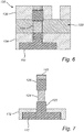
- Figure 6 shows that the gate stack 180 has enclosed the channel portion 124 of the vertical semiconductor structure 120.
- the gate stack 180 may comprise a gate dielectric wrapping around the channel portion 124 and a gate electrode wrapping around the gate dielectric (not shown in Figure 6 ).
- the gate dielectric and the gate electrode may be formed in manner which per se is known the art.
- the gate dielectric layer may for example be formed by any conventional gate dielectric material such as HfO 2 , ZrO 2 , Al 2 O 3 or some other high-K dielectric material.
- the gate dielectric layer may be deposited as a conformal thin film by any conventional deposition process, for instance by atomic layer deposition (ALD).
- the gate electrode may comprise one or more metals, such as a an effective work function metal (EWF) in combination with a fill metal.
- EWF effective work function metal
- the gate electrode may comprise one or more p-type EWF metals such as TiN, TaN, TiTaN or one or more n-type EWF metals such as Al, TiAl, TiC, or TiAlC, or compound layers such as TiN/TiAl or TiN/TaN/TiAl. Any remaining space in the cavity 174 may be filled with a fill metal such as W or Co.
- the method may thereafter proceed with forming source/drain contacts in a manner which per se is known in the art.
- Figures 7-9 show another method for forming a VFET device.
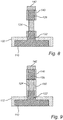
- Figure 7 shows that a cross-sectional dimension of the channel portion 124 has been reduced, prior to forming the sacrificial structure 160.
- the cross-sectional dimension of the channel portion may be reduced by selective etching the channel portion 124 with respect to the upper and lower source/drain portions 126, 122 thanks to their different compositions.
- the selective etching of the channel portion 124 may be performed in e.g. a wet etching process that selectively etches the channel portion 124 material with respect to the lower and upper source/drain portions 122, 126.
- the amount of trimming may be controlled by e.g. controlling the etching time.
- the method may thereafter proceed as shown in Figure 8 , by forming the spacer 140 on peripheral surfaces of the lower and upper source/drain portions 122, 126 of the vertical semiconductor structure 120, and then as shown in Figure 9 by forming the stressor layer 150 on the channel portion 124 of the reduced cross-sectional dimension.
- the method may thereafter proceed in the same manner as shown in Figures 4-6 and described above.
- the reduction of the cross-sectional dimension of the channel portion 124 may alternatively be performed subsequent to the formation of the spacer 140 on peripheral surfaces of the lower and upper source/drain portions 122,126. In this way, the upper and lower source/drain portions 126,122 may be masked by the spacer 140 during the etching of the channel portion 124.
- the stressor layer 150 may subsequently be formed to enclose the channel portion 124 of the reduced cross-sectional dimension, as disclosed above.
Landscapes
- Insulated Gate Type Field-Effect Transistor (AREA)
Abstract
According to an aspect of the present inventive concept there is provided a method for forming a vertical field-effect transistor device. The method comprises forming on a substrate a vertical semiconductor structure protruding above the substrate and comprising a lower source/drain portion, an upper source/drain portion and a channel portion arranged between the lower source/drain portion and the upper source/drain portion, forming on the channel portion an epitaxial semiconductor stressor layer enclosing the channel portion, wherein the stressor layer and the channel portion are lattice mismatched, forming an insulating layer and a sacrificial structure, wherein the sacrificial structure encloses the channel portion with the stressor layer formed thereon and wherein the insulating layer embeds the semiconductor structure and the sacrificial structure, forming in the insulating layer an opening exposing a surface portion of the sacrificial structure, etching the sacrificial structure through the opening in the insulating layer, thereby forming a cavity exposing the stressor layer enclosing the channel portion, subsequent to etching the sacrificial structure, etching the stressor layer in the cavity, and subsequent to etching the stressor layer, forming a gate stack in the cavity, the gate stack enclosing the channel portion of the vertical semiconductor structure.
Description
- The present inventive concept relates to a method for forming a vertical field-effect transistor device.
- A vertical field effect transistor (VFET) is a device comprising a vertical semiconductor structure, such as a vertical nanowire or nanosheet, protruding above the substrate. The VFET has a vertically oriented channel defined in a channel portion of the semiconductor structure, the channel portion extending between a lower and an upper source/drain portion. A VFET may hence be referred to as a vertical channel device. The gate of the VFET extends around the channel portion, typically in an all-around fashion. In contrast to horizontal channel devices such as planar FETs and finFETs where the gate length is defined by the line width of the gate, the gate length of a VFET is defined along the thickness direction of the gate layer. For this reason, among others, the VFET is an enabler for dense circuit implementations.
- Strain engineering is concerned with improving device performance, such as carrier mobility, by introducing strain into e.g. the semiconductor channel portion. Although much attention has gone into development of strain engineering techniques for horizontal channel devices, there is a need for novel strain engineering techniques for VFETs.
- An objective of the present inventive concept is to address this need. Further and alternative objectives may be understood from the following.
- According to an aspect of the present inventive concept there is provided a method for forming a vertical field-effect transistor device, the method comprising:
- forming on a substrate a vertical semiconductor structure protruding above the substrate and comprising a lower source/drain portion, an upper source/drain portion and a channel portion arranged between the lower source/drain portion and the upper source/drain portion,
- forming on the channel portion an epitaxial semiconductor stressor layer enclosing the channel portion, wherein the stressor layer and the channel portion are lattice mismatched,
- forming an insulating layer and a sacrificial structure, wherein the sacrificial structure encloses the channel portion with the stressor layer formed thereon and wherein the insulating layer embeds the semiconductor structure and the sacrificial structure, forming in the insulating layer an opening exposing a surface portion of the sacrificial structure,
- etching the sacrificial structure through the opening in the insulating layer, thereby forming a cavity exposing the stressor layer enclosing the channel portion,
- subsequent to etching the sacrificial structure, etching the stressor layer in the cavity, and
- subsequent to etching the stressor layer, forming a gate stack in the cavity, the gate stack enclosing the channel portion of the vertical semiconductor structure.
- The present inventive concept allows providing a lattice-mismatched heterojunction between the channel portion and the stressor layer. Thereby, strain may be applied to the channel portion. By etching the stressor layer prior to forming the gate stack, the stressor layer may be reduced in thickness, or preferably such that the channel portion is exposed. Hence, the stressor layer need neither result in any appreciable increase in cross-sectional dimension of the channel portion nor an associated reduction of channel control. Due to presence of the embedding insulating layer the strain introduced by the stressor layer may be preserved in the channel portion also after the etching of the stressor layer. The presence of the strain in the channel portion may hence increase carrier mobility in the channel of the obtained VFET device.
- The insulating layer may comprise a lower insulating layer portion, formed prior to the sacrificial structure, embedding the lower source/drain portion at least partly and exposing the channel portion. The insulating layer may further comprise an upper insulating layer portion, formed subsequent to the sacrificial structure, embedding the sacrificial structure and the upper source/drain portion at least partly. The sacrificial structure may be formed on the lower insulating layer portion. Thereby, the sacrificial structure may be embedded or surrounded both vertically and laterally by the insulating layer. By forming the sacrificial structure subsequent to the lower insulating layer the final gate structure may be electrically insulated from the substrate below.
- Forming the sacrificial structure may comprise depositing a sacrificial layer on the lower insulating layer portion, and patterning the sacrificial layer to define said sacrificial structure prior to forming the upper insulating layer portion. Thereby, the patterning of the sacrificial layer into the sacrificial structure may enable formation of the sacrificial structure with desired dimensions. As may be appreciated, the sacrificial structure may hence be formed as a sacrificial gate structure or dummy gate structure.
- The opening formed in the insulating layer may be formed in the upper insulating layer portion. The opening may be formed by etching the upper insulating layer until exposing an upper surface of the sacrificial structure.
- The channel portion may comprise Si1-xGex and the stressor layer may comprise Si1-yGey wherein x differs from y. Depending on whether x is smaller or greater than y either compressive or tensile strain may be introduced into the channel portion. Advantageously, for fabrication of an n-type VFET, x may be smaller than y. A higher Ge content of the stressor layer (y) than the channel portion (x) may provide a lattice-mismatched heterojunction between the channel portion and the stressor layer introducing tensile strain. The amount and type of strain introduced into the channel portion may more generally be tuned by controlling the relative compositions of the channel portion and the stressor layer.
- The lower source/drain portion may comprise Si1-aGea and the upper source/drain portion may comprise Si1-bGeb wherein a and b differ from x. This allows selective processing of the channel and source/drain portions. It may further allow introducing different amounts of strain in the channel portion and the source portion and/or drain portion, if the stressor layer is formed on also the source portion and/or drain portion.
- The Ge content a and b may be equal to each other or different.
- The Ge content of the source/drain portions may be greater than the Ge content of the channel portion, i.e. a > x and b > x. An advantage brought about by having a higher Ge content in the lower and upper source/drain portions than in the channel portion is that even if the stressor layer is formed on all three portions of the vertical semiconductor structure, a greater strain may be provided to the channel portion.
- The method may further comprise, prior to forming the sacrificial structure, reducing a cross-sectional dimension of the channel portion by etching said channel portion selectively to said upper and lower source/drain portions. Thereby, channel control of the VFET device may be further improved. Reducing the cross-sectional dimensions of the channel portion (i.e. "trimming" the channel portion) may further facilitate introducing strain in to a greater part of the channel portion.
- The method may further comprise, prior to forming the insulating layer and the sacrificial structure, forming a spacer on peripheral surfaces of the lower and upper source/drain portions. Thereby, the spacers may counteract formation of the stressor layer on the lower and upper source/drain portions and may hence enable selective formation of the stressor layer on only the channel portion.
- Forming the spacer may comprise subjecting the vertical semiconductor structure to an oxidation process, thereby forming an oxide layer on peripheral surfaces of the lower and upper source/drain portions, such that the lower and upper source/drain portions may be provided with thicker oxide layer portions than the channel portion. The method may subsequently comprise etching the oxide layer to expose the channel portion while preserving at least some of the oxide layer at the lower and upper source/drain portions.
- The thicker oxide layer on the lower and upper source/drain portions than the channel portion may be achieved due to the higher oxidation rate of the lower and upper source/drain portions than the channel portion. The higher oxidation rate of the lower and upper source/drain portions than the channel portion may be provided by a higher Ge contents of them. Thereby, a compositional tuning of the lower source/drain portion, the channel portion and the upper source/drain portion may advantageously facilitate formation of the spacers on the lower and upper source/drain portions to counteract the stressor layer formation thereon.
- The method may further comprise, subsequent to forming the spacer, reducing a cross-sectional dimension of the channel portion by etching said channel portion selectively to said upper and lower source/drain portions, and subsequently forming the stressor layer enclosing the channel portion of the reduced cross-sectional dimension. Thereby the spacer may advantageously be used to counteract reduction of the cross-sectional dimension of the lower and upper source/drain portions and hence enable a highly selective reduction of the cross-sectional dimension of the channel portion with respect to the lower and upper source/drain portions. The reduction of the cross-sectional dimension of the channel portion may allow further improved channel control of the VFET device and further facilitate introducing a greater amount of strain in the channel portion.
- The above, as well as additional objects, features and advantages of the present inventive concept, will be better understood through the following illustrative and non-limiting detailed description, with reference to the appended drawings. In the drawings like reference numerals will be used for like elements unless stated otherwise.
-
Figures 1-9 schematically illustrate various methods for forming a vertical field-effect transistor device. - Various methods for forming a vertical field-effect transistor device will now be disclosed in connection with
figures 1-9 . -
Figure 1 shows a cross-sectional view of aninitial structure 100 of the method. Thestructure 100 comprises avertical semiconductor structure 120 which protrudes above asubstrate 110. InFigure 1 , the axis Y denotes a vertical direction corresponding to a normal direction with respect to an upper surface of thesubstrate 110. The axis X denotes a first horizontal direction along thesubstrate 110 and the axis Z denotes a second horizontal direction along thesubstrate 110, perpendicular to the first direction X. It should be noted that in the drawings the relative dimensions of the shown elements, such as the height, width or thickness of elements, is merely schematic and may, for the purpose of illustrational clarity, differ from a physical structure. - In
Figure 1 and the following figures, onevertical semiconductor structure 120 is shown. However, it should be noted that there may be any number of furthervertical semiconductor structures 120 above the substrate 110 (outside the illustrated region). Thevertical semiconductor structure 120 extends in parallel to the Y direction. By way of example, a typical height of thevertical semiconductor structure 120 may be in a range from 10 to 200 nm. The width of the vertical semiconductor structure 120 (i.e. along the X axis) may be in a range from 3 to 100 nm. The width of avertical semiconductor structure 120 in the second horizontal direction (i.e. along the Z axis) may be in a range from 3 to 100 nm, e.g. depending on whether a nanowire-shaped or nanosheet-shaped structure is desired. - The
substrate 110 may be anyconventional substrate 110, such as a substrate suitable for complementary metal-oxide semiconductor (CMOS) processing. Thesubstrate 110 may for instance be a semiconductor substrate such as a Si substrate, a Ge substrate or a silicon-germanium (SiGe) substrate. Other examples include a silicon-on-insulator (SOI) substrate, a GeOI substrate or a SiGeOI substrate. - The
vertical semiconductor structure 120 comprises a lower source/drain portion 122, an upper source/drain portion 126 and achannel portion 124 arranged between the lower and upper source/drain portion drain portion 122, thechannel portion 124 and the upper source/drain portion 126 form a stack of three segments along the Y direction. The lower source/drain portion 122, thechannel portion 124 and the upper source/drain portion 126 may have the same or different height/thickness. A typical height of the lower and upper source/drain portions - The
channel portion 124 may be formed of Si or a Si1-xGex alloy with a low Ge content such as x being in a range from 0 to 20%. The lower source/drain portion 122 may be formed of Si1-aGea alloy where a may be greater than x. As an example a may be in a range of 20%-80%. The upper source/drain portion 126 may be formed of Si1-bGeb alloy where b may be greater than x. As an example b may be in a range of 20%-80%. It is however also contemplated that thechannel portion 124 may be formed with a greater Ge-content than the source/drain portions channel portion 124 may be formed of Si1-xGex with x in a range from 80 to 100%, and the lower and upper source/drain portions being formed of Si1-aGea and Si1-bGeb respectively, where a and b are in a range from 0 to 20%. - The
vertical semiconductor structure 120 may be formed in a manner which per se is known in the art, e.g. by etching an epitaxial semiconductor layer stack formed on thesubstrate 110, the layer stack comprising a lower source/drain layer, a channel layer and an upper source/drain layer. The layer stack may be formed using any suitable conventional technique, such as chemical vapor deposition (CVD), metalorganic CVD (MOCVD), molecular beam epitaxy (MBE) or vapor phase epitaxy (VPE).Reference sign 142 inFigure 1 signifies a mask which may remain after the patterning of thesemiconductor structure 120. Themask 142 may for instance be a hard mask or an oxide mask. Themask 142 may protect the upper surface of the upper source/drain portion 126 during subsequent method steps, to be described below. - Subsequent to forming the
vertical semiconductor structure 120, a bottom portion of thevertical semiconductor structure 120 may be embedded in a "bottom insulatinglayer 132". The bottom insulatinglayer 132 may cover thesubstrate 110 in regions adjacent to and in between the vertical semiconductor structure(s) 120. An insulating material, e.g. an oxide material such as silicon dioxide or a low-k dielectric material, may be deposited and etched back to define a layer of a desired thickness. The bottom insulatinglayer 132 may for instance form a shallow-trench-insulation (STI), embedding lower portions of vertical semiconductor structure(s) 120. The insulating layer may be formed for instance using CVD. - In
Figure 2 , aspacer 140 has been formed on peripheral surfaces of the lower and upper source/drain portions 122,126 of thevertical semiconductor structure 120. Thespacer 140 may be formed by subjecting thevertical semiconductor structure 120 to an oxidation process in which an oxide layer is formed. - As disclosed above, the
channel portion 124 may be formed of a different material than the lower and upper source/drain portions drain portions channel portion 124 enables a selective or at least preferential oxidation of the lower and upper source/drain portions drain portions channel portion 124. The oxide may thus be formed at a temperature and pressure selected such that the thickness of the oxide is growing faster on the lower and upper source/drain portions channel portion 124. In this way, a thicker spacer layer may be produced on the peripheral surfaces of the lower and upper source/drain portions channel portion 124. A uniform etch of the spacer layer may result in an etch back of the spacer layer such that the peripheral surface of thechannel portion 124 is exposed, while a (thinned) spacer layer remains on the peripheral surfaces of the lower and upper source/drain portions spacers 140 may be formed on the lower and upper source/drain portions - The method proceeds by forming on the
channel portion 124 an epitaxialsemiconductor stressor layer 150, as shown inFigure 3 . Thestressor layer 150 may enclose thechannel portion 124 by covering a peripheral surface of thechannel portion 124. Thestressor layer 150 is formed to be lattice mismatched with respect to thechannel portion 124. The lattice mismatch induces strain in the lattice structure of thechannel portion 124. The type of strain (i.e. tensile or compressive) may generally depend on the relative compositions of thestressor layer 150 and thechannel portion 124. If thestressor layer 150 has a greater Ge-content than thechannel portion 124, tensile strain may be induced in thechannel portion 124. Tensile strain may be desired for fabrication of n-type VFETs. If thestressor layer 150 has a lower Ge-content than thechannel portion 124, compressive strain may be induced in thechannel portion 124. Compressive strain may be desired for fabrication of p-type VFETs. The net direction of the strain may typically be oriented in a vertically upward or downward direction. -
Figure 3 shows that nostressor layer 150 has been formed on the lower and the upper source/drain portions spacer 140 may counteract formation of thestressor layer 150 on the lower and upper source/drain portions - The epitaxial semiconductor stressor layer may be formed for instance by using MBE or standard CVD. The
stressor layer 150 may be formed of Si1-yGey alloy wherein y may be in a range of 20%-80%, however in any case different from the composition of thechannel layer 124. Thestressor layer 150 may for instance be formed with a thickness in a range of 1 to 10 nm. The composition of thestressor layer 150 may be determined by e.g. selecting appropriate precursors controlling epitaxial growth parameters e.g. flows and temperature. - The method proceeds by forming an insulating
layer 130 and asacrificial structure 160, as shown inFigure 4. Figure 4 shows that the insulatinglayer 130 has embedded thesemiconductor structure 120 and thesacrificial structure 160. - The insulating
layer 130 may comprise a lower insulatinglayer 134 and an upper insulatinglayer 136. The lowerinsulating layer 134 may be formed prior to thesacrificial structure 160. The lowerinsulating layer 134 may completely or at least partly embed the lower source/drain portion 122 while exposing thechannel portion 124. As suggested byFigure 4 , the lower insulatinglayer 134 may be formed of the same material as the bottom insulatinglayer 132 such that they may form a common lowerinsulating layer 134. However, it would also be possible to form the insulatinglayer 134 of a material different than the bottom insulatinglayer 132. The lowerinsulating layer 134 may be formed in a similar manner as the bottom insulatinglayer 132, e.g. by depositing insulating material and subsequently performing an etch back of the deposited insulating material such that an upper surface of the lower insulatinglayer 134 may correspond at least roughly to a level of the interface between the lower source/drain portion 122 and thechannel portion 124. - The
sacrificial structure 160 may be formed subsequent to the lower insulatinglayer portion 134. Thesacrificial structure 160 may be formed on the lower insulatinglayer portion 134.Figure 4 shows that thesacrificial structure 160 encloses thechannel portion 124 with thestressor layer 150 formed thereon. Thesacrificial structure 160 may be formed by depositing a sacrificial layer on the lower insulatinglayer portion 134, for instance a layer of amorphous Si, however some other suitable material which may be removed selectively from thespacer 140 material and the insulatinglayer 130 would also be possible. The sacrificial layer may subsequently be patterned to define thesacrificial structure 160. Preferably, thesacrificial structure 160 may be defined with dimensions corresponding to desired dimensions of a final gate structure, which is to be formed. - The upper insulating
layer portion 136 may be formed subsequent to thesacrificial structure 160. The upper insulatinglayer portion 136 may completely embed and cover thesacrificial structure 160. The upper insulatinglayer portion 136 may also embed the upper source/drain portion 126. The upper insulatinglayer portion 136 may be formed in a similar manner, and also by a same material as the lower insulatinglayer portion 134. Insulating material may be deposited to embed and cover thesacrificial structure 160 and the upper source/drain portion 126. The deposited insulating material may subsequently be planarized (e.g. by CMP) and etched back to become co-planar with an upper surface of themask 142. -
Figure 4 shows that anopening 172 has been formed in the insulatinglayer 130. Theopening 172 exposes a surface portion of thesacrificial structure 160, e.g. an upper surface portion as shown. Theopening 172 ofFigure 4 has been formed in the upper insulatinglayer portion 136. Theopening 172 may be formed e.g. by etching the upper insulatinglayer 136 through a lithographically patterned etch mask. - As shown in
Figure 4 , theopening 172 provides access to thesacrificial structure 160 and the method proceeds by etching thesacrificial structure 160 through theopening 172 in the insulatinglayer 130.Figure 5 shows that thesacrificial structure 160 has been removed selectively with respect to the lower and upper insulatinglayer portions cavity 174 within the insulatinglayer 130. The etching of thesacrificial structure 160 proceeds until thestressor layer 150 enclosing thechannel portion 124 is exposed. The etching of thesacrificial structure 160 may be performed in a wet or vapor etching process. For instance, a wet etching process using Tetramethylammonium hydroxide (TMAH) may be performed at a temperature higher than room temperature e.g. 80° C to etch thesacrificial structure 160. Examples of dry etching processes include SF6 or CF4 based plasmas. - The method further proceeds by etching the
stressor layer 150 in thecavity 174, subsequent to etching thesacrificial structure 160. As shown inFigure 5 thestressor layer 150 may be removed to expose the peripheral surface of thechannel portion 124. As the lower and upper source/drain portions layer 130, the strain in thechannel portion 124 may be preserved also following the removal of thestressor layer 150. Although shown to be completely removed inFigure 5 , it is also possible to only partially reduce a thickness of thestressor layer 150 such that astressor layer 150 of a reduced thickness remain on thechannel portion 150. Advantageously, an etching process allowing thestressor layer 150 to be etched selectively from thechannel portion 124 may be used. However, a non-selective etching is also viable by timing the etching process appropriately. - In any case, the method may further proceed by forming a
gate stack 180 in thecavity 174 subsequent to the etching of thestressor layer 150.Figure 6 shows that thegate stack 180 has enclosed thechannel portion 124 of thevertical semiconductor structure 120. Thegate stack 180 may comprise a gate dielectric wrapping around thechannel portion 124 and a gate electrode wrapping around the gate dielectric (not shown inFigure 6 ). The gate dielectric and the gate electrode may be formed in manner which per se is known the art. The gate dielectric layer may for example be formed by any conventional gate dielectric material such as HfO2, ZrO2, Al2O3 or some other high-K dielectric material. The gate dielectric layer may be deposited as a conformal thin film by any conventional deposition process, for instance by atomic layer deposition (ALD). The gate electrode may comprise one or more metals, such as a an effective work function metal (EWF) in combination with a fill metal. By way of example the gate electrode may comprise one or more p-type EWF metals such as TiN, TaN, TiTaN or one or more n-type EWF metals such as Al, TiAl, TiC, or TiAlC, or compound layers such as TiN/TiAl or TiN/TaN/TiAl. Any remaining space in thecavity 174 may be filled with a fill metal such as W or Co. The method may thereafter proceed with forming source/drain contacts in a manner which per se is known in the art. -
Figures 7-9 show another method for forming a VFET device.Figure 7 shows that a cross-sectional dimension of thechannel portion 124 has been reduced, prior to forming thesacrificial structure 160. The cross-sectional dimension of the channel portion may be reduced by selective etching thechannel portion 124 with respect to the upper and lower source/drain portions channel portion 124 may be performed in e.g. a wet etching process that selectively etches thechannel portion 124 material with respect to the lower and upper source/drain portions - The method may thereafter proceed as shown in
Figure 8 , by forming thespacer 140 on peripheral surfaces of the lower and upper source/drain portions vertical semiconductor structure 120, and then as shown inFigure 9 by forming thestressor layer 150 on thechannel portion 124 of the reduced cross-sectional dimension. The method may thereafter proceed in the same manner as shown inFigures 4-6 and described above. - The reduction of the cross-sectional dimension of the
channel portion 124 may alternatively be performed subsequent to the formation of thespacer 140 on peripheral surfaces of the lower and upper source/drain portions 122,126. In this way, the upper and lower source/drain portions 126,122 may be masked by thespacer 140 during the etching of thechannel portion 124. Thestressor layer 150 may subsequently be formed to enclose thechannel portion 124 of the reduced cross-sectional dimension, as disclosed above. - In the above the inventive concept has mainly been described with reference to a limited number of examples. However, as is readily appreciated by a person skilled in the art, other examples than the ones disclosed above are equally possible within the scope of the inventive concept, as defined by the appended claims.
Claims (10)
- A method for forming a vertical field-effect transistor device, the method comprising:forming on a substrate (110) a vertical semiconductor structure (120) protruding above the substrate (110) and comprising a lower source/drain portion (122), an upper source/drain portion (126) and a channel portion (124) arranged between the lower source/drain portion (122) and the upper source/drain portion (126),forming on the channel portion (124) an epitaxial semiconductor stressor layer (150) enclosing the channel portion (124), wherein the stressor layer (150) and the channel portion (124) are lattice mismatched,forming an insulating layer (130) and a sacrificial structure (160), wherein the sacrificial structure (160) encloses the channel portion (124) with the stressor layer (150) formed thereon and wherein the insulating layer (130) embeds the semiconductor structure (120) and the sacrificial structure (160),forming in the insulating layer (130) an opening (172) exposing a surface portion of the sacrificial structure (160),etching the sacrificial structure (160) through the opening (172) in the insulating layer (130), thereby forming a cavity (174) exposing the stressor layer (150) enclosing the channel portion (124),subsequent to etching the sacrificial structure (160), etching the stressor layer (150) in the cavity (174), andsubsequent to etching the stressor layer (150), forming a gate stack (180) in the cavity (174), the gate stack (180) enclosing the channel portion (124) of the vertical semiconductor structure (120).
- A method according to claim 1, wherein the insulating layer (130) comprises:a lower insulating layer portion (134), formed prior to the sacrificial structure (160), embedding the lower source/drain portion (122) at least partly and exposing the channel portion (124), andan upper insulating layer portion (136), formed subsequent to the sacrificial structure (160), embedding the sacrificial structure (160) and the upper source/drain portion (126) at least partly,wherein the sacrificial structure (160) is formed on the lower insulating layer portion (134).
- A method according to claim 2, wherein forming the sacrificial structure (160) comprises:depositing a sacrificial layer on the lower insulating layer portion (134), andpatterning the sacrificial layer to define said sacrificial structure (160) prior to forming the upper insulating layer portion (136).
- A method according to any of claims 2-3, wherein the opening (172) formed in the insulating layer (130) is formed in the upper insulating layer portion (136).
- A method according to any preceding claim, wherein the channel portion (124) comprises Si1-xGex and the stressor layer (150) comprises Si1-yGey wherein x differs from y.
- A method according to claim 5, wherein the lower source/drain portion (122) comprises Si1-aGea and the upper source/drain portion (126) comprises Si1-bGeb wherein a and b differ from x.
- A method according to claim 6, further comprising, prior to forming the sacrificial structure (160), reducing a cross-sectional dimension of the channel portion (124) by etching said channel portion (124) selectively to said upper and lower source/drain portions (126,122).
- A method according to any preceding claim, the method further comprising, prior to forming the insulating layer (130) and the sacrificial structure (160), forming a spacer (140) on peripheral surfaces of the lower and upper source/drain portions (122,126).
- A method according to claim 8, wherein forming the spacer (140) comprises subjecting the vertical semiconductor structure (120) to an oxidation process, thereby forming an oxide layer on peripheral surfaces of the lower and upper source/drain portions (122,126), such that the lower and upper source/drain portions (122,126) are provided with thicker oxide layer portions than the channel portion (124), and subsequently etching the oxide layer to expose the channel portion (124) while preserving at least some of the oxide layer at the lower and upper source/drain portions (122,126).
- A method according to any of claims 8-9, further comprising, subsequent to forming the spacer (140), reducing a cross-sectional dimension of the channel portion (124) by etching said channel portion (124) selectively to said upper and lower source/drain portions (126,122), and subsequently forming the stressor layer (150) enclosing the channel portion (124) of the reduced cross-sectional dimension.
Priority Applications (3)
| Application Number | Priority Date | Filing Date | Title |
|---|---|---|---|
| EP19178418.0A EP3748683A1 (en) | 2019-06-05 | 2019-06-05 | A method for forming a verical field-effect transistor device |
| CN202010489213.0A CN112053955A (en) | 2019-06-05 | 2020-06-02 | A method of forming a vertical field effect transistor device |
| US16/893,233 US11088263B2 (en) | 2019-06-05 | 2020-06-04 | Method of forming vertical field effect transistor device |
Applications Claiming Priority (1)
| Application Number | Priority Date | Filing Date | Title |
|---|---|---|---|
| EP19178418.0A EP3748683A1 (en) | 2019-06-05 | 2019-06-05 | A method for forming a verical field-effect transistor device |
Publications (1)
| Publication Number | Publication Date |
|---|---|
| EP3748683A1 true EP3748683A1 (en) | 2020-12-09 |
Family
ID=66776102
Family Applications (1)
| Application Number | Title | Priority Date | Filing Date |
|---|---|---|---|
| EP19178418.0A Withdrawn EP3748683A1 (en) | 2019-06-05 | 2019-06-05 | A method for forming a verical field-effect transistor device |
Country Status (3)
| Country | Link |
|---|---|
| US (1) | US11088263B2 (en) |
| EP (1) | EP3748683A1 (en) |
| CN (1) | CN112053955A (en) |
Families Citing this family (2)
| Publication number | Priority date | Publication date | Assignee | Title |
|---|---|---|---|---|
| CN114420751B (en) * | 2021-12-06 | 2025-07-29 | 北京超弦存储器研究院 | Vertical MOSFET device and manufacturing method and application thereof |
| CN116825838B (en) * | 2022-03-17 | 2026-01-23 | 长鑫存储技术有限公司 | Semiconductor structure and manufacturing method thereof, memory and manufacturing method thereof |
Citations (2)
| Publication number | Priority date | Publication date | Assignee | Title |
|---|---|---|---|---|
| US20130270628A1 (en) * | 2012-04-13 | 2013-10-17 | Taiwan Semiconductor Manufacturing Co., Ltd. | Replacement Channels |
| US10014372B1 (en) * | 2017-01-05 | 2018-07-03 | International Business Machines Corporation | Vertical gate-all-around transistor with top and bottom source/drain epitaxy on a replacement nanowire, and method of manufacturing the same |
Family Cites Families (15)
| Publication number | Priority date | Publication date | Assignee | Title |
|---|---|---|---|---|
| KR100960928B1 (en) | 2008-01-02 | 2010-06-07 | 주식회사 하이닉스반도체 | Vertical transistors and their formation |
| KR20150020848A (en) | 2013-08-19 | 2015-02-27 | 에스케이하이닉스 주식회사 | PMOS Transistor Improved Current-drivability With Vertical Channel, Variable Resistive Memory Device Including the same And Method of Manufacturing PMOS Transistor |
| US9911848B2 (en) * | 2014-08-29 | 2018-03-06 | Taiwan Semiconductor Manufacturing Co., Ltd. | Vertical transistor and method of manufacturing the same |
| US20160240623A1 (en) * | 2015-02-13 | 2016-08-18 | Taiwan Semiconductor Manufacturing Company, Ltd. | Vertical gate all around (vgaa) devices and methods of manufacturing the same |
| US9882047B2 (en) * | 2016-02-01 | 2018-01-30 | International Business Machines Corporation | Self-aligned replacement metal gate spacerless vertical field effect transistor |
| US9755073B1 (en) | 2016-05-11 | 2017-09-05 | International Business Machines Corporation | Fabrication of vertical field effect transistor structure with strained channels |
| US9870957B2 (en) * | 2016-06-16 | 2018-01-16 | Samsung Electronics Co., Ltd. | Vertical fin field effect transistor (V-FinFET), semiconductor device having V-FinFET and method of fabricating V-FinFET |
| US9929152B2 (en) * | 2016-06-30 | 2018-03-27 | Globalfoundries Inc. | Vertical transistors and methods of forming same |
| US11056391B2 (en) * | 2016-06-30 | 2021-07-06 | International Business Machines Corporation | Subtractive vFET process flow with replacement metal gate and metallic source/drain |
| US10347745B2 (en) * | 2016-09-19 | 2019-07-09 | Globalfoundries Inc. | Methods of forming bottom and top source/drain regions on a vertical transistor device |
| US9947789B1 (en) | 2016-10-17 | 2018-04-17 | Globalfoundries Inc. | Vertical transistors stressed from various directions |
| CN108695382B (en) * | 2017-04-07 | 2021-07-06 | 中芯国际集成电路制造(上海)有限公司 | Semiconductor device and method of manufacturing the same |
| CN108878521B (en) * | 2017-05-09 | 2021-10-15 | 中芯国际集成电路制造(上海)有限公司 | Vertical tunneling field effect transistor and method of forming the same |
| US10170376B1 (en) * | 2017-10-22 | 2019-01-01 | United Microelectronics Corp. | Device and forming method thereof |
| US10600695B2 (en) * | 2018-05-22 | 2020-03-24 | International Business Machines Corporation | Channel strain formation in vertical transport FETS with dummy stressor materials |
-
2019
- 2019-06-05 EP EP19178418.0A patent/EP3748683A1/en not_active Withdrawn
-
2020
- 2020-06-02 CN CN202010489213.0A patent/CN112053955A/en active Pending
- 2020-06-04 US US16/893,233 patent/US11088263B2/en not_active Expired - Fee Related
Patent Citations (2)
| Publication number | Priority date | Publication date | Assignee | Title |
|---|---|---|---|---|
| US20130270628A1 (en) * | 2012-04-13 | 2013-10-17 | Taiwan Semiconductor Manufacturing Co., Ltd. | Replacement Channels |
| US10014372B1 (en) * | 2017-01-05 | 2018-07-03 | International Business Machines Corporation | Vertical gate-all-around transistor with top and bottom source/drain epitaxy on a replacement nanowire, and method of manufacturing the same |
Also Published As
| Publication number | Publication date |
|---|---|
| CN112053955A (en) | 2020-12-08 |
| US11088263B2 (en) | 2021-08-10 |
| US20200388698A1 (en) | 2020-12-10 |
Similar Documents
| Publication | Publication Date | Title |
|---|---|---|
| US10930764B2 (en) | Extension region for a semiconductor device | |
| US9373704B2 (en) | Multiple-gate semiconductor device and method | |
| US11682591B2 (en) | Method for forming transistor structures | |
| US11043587B2 (en) | Fabrication of vertical fin transistor with multiple threshold voltages | |
| US9224865B2 (en) | FinFET with insulator under channel | |
| US10217672B2 (en) | Vertical transistor devices with different effective gate lengths | |
| US9006805B2 (en) | Semiconductor device | |
| US20040173815A1 (en) | Strained-channel transistor structure with lattice-mismatched zone | |
| US9620506B2 (en) | Silicon-on-nothing transistor semiconductor structure with channel epitaxial silicon region | |
| KR20060130166A (en) | How to form a semiconductor device with local SOU | |
| US20150137181A1 (en) | Stress inducing contact metal in finfet cmos | |
| US20060186470A1 (en) | Strained transistor with hybrid-strain inducing layer | |
| US12237371B2 (en) | Method for forming a semiconductor device | |
| US11088263B2 (en) | Method of forming vertical field effect transistor device | |
| KR102155327B1 (en) | Field effect transistor and methods for manufacturing the same | |
| EP3719847A1 (en) | A method for forming vertical nanowire or nanosheet field-effect transistors simultaneous with horizontal field-effect transistors | |
| US8779525B2 (en) | Method for growing strain-inducing materials in CMOS circuits in a gate first flow | |
| US10892181B2 (en) | Semiconductor device with mitigated local layout effects | |
| EP3675159B1 (en) | A semiconductor structure and a method for cutting a semiconductor fin | |
| KR102422158B1 (en) | Semiconductor device and method for manufacturing the same | |
| US20250212494A1 (en) | Method for Forming a Semiconductor Structure | |
| US20200312725A1 (en) | Method of forming a semiconductor device |
Legal Events
| Date | Code | Title | Description |
|---|---|---|---|
| PUAI | Public reference made under article 153(3) epc to a published international application that has entered the european phase |
Free format text: ORIGINAL CODE: 0009012 |
|
| STAA | Information on the status of an ep patent application or granted ep patent |
Free format text: STATUS: THE APPLICATION HAS BEEN PUBLISHED |
|
| AK | Designated contracting states |
Kind code of ref document: A1 Designated state(s): AL AT BE BG CH CY CZ DE DK EE ES FI FR GB GR HR HU IE IS IT LI LT LU LV MC MK MT NL NO PL PT RO RS SE SI SK SM TR |
|
| AX | Request for extension of the european patent |
Extension state: BA ME |
|
| STAA | Information on the status of an ep patent application or granted ep patent |
Free format text: STATUS: THE APPLICATION IS DEEMED TO BE WITHDRAWN |
|
| 18D | Application deemed to be withdrawn |
Effective date: 20210610 |