EP3745602A1 - Communication system and transmission device - Google Patents
Communication system and transmission device Download PDFInfo
- Publication number
- EP3745602A1 EP3745602A1 EP19744498.7A EP19744498A EP3745602A1 EP 3745602 A1 EP3745602 A1 EP 3745602A1 EP 19744498 A EP19744498 A EP 19744498A EP 3745602 A1 EP3745602 A1 EP 3745602A1
- Authority
- EP
- European Patent Office
- Prior art keywords
- signal
- communication system
- transmission
- branch point
- signal line
- Prior art date
- Legal status (The legal status is an assumption and is not a legal conclusion. Google has not performed a legal analysis and makes no representation as to the accuracy of the status listed.)
- Granted
Links
Images






Classifications
-
- H—ELECTRICITY
- H04—ELECTRIC COMMUNICATION TECHNIQUE
- H04B—TRANSMISSION
- H04B3/00—Line transmission systems
- H04B3/54—Systems for transmission via power distribution lines
-
- H—ELECTRICITY
- H01—ELECTRIC ELEMENTS
- H01P—WAVEGUIDES; RESONATORS, LINES, OR OTHER DEVICES OF THE WAVEGUIDE TYPE
- H01P5/00—Coupling devices of the waveguide type
- H01P5/12—Coupling devices having more than two ports
- H01P5/16—Conjugate devices, i.e. devices having at least one port decoupled from one other port
- H01P5/18—Conjugate devices, i.e. devices having at least one port decoupled from one other port consisting of two coupled guides, e.g. directional couplers
-
- H—ELECTRICITY
- H04—ELECTRIC COMMUNICATION TECHNIQUE
- H04B—TRANSMISSION
- H04B3/00—Line transmission systems
- H04B3/02—Details
-
- H—ELECTRICITY
- H04—ELECTRIC COMMUNICATION TECHNIQUE
- H04B—TRANSMISSION
- H04B3/00—Line transmission systems
- H04B3/02—Details
- H04B3/04—Control of transmission; Equalising
-
- H—ELECTRICITY
- H04—ELECTRIC COMMUNICATION TECHNIQUE
- H04L—TRANSMISSION OF DIGITAL INFORMATION, e.g. TELEGRAPHIC COMMUNICATION
- H04L25/00—Baseband systems
- H04L25/02—Details ; arrangements for supplying electrical power along data transmission lines
-
- H—ELECTRICITY
- H04—ELECTRIC COMMUNICATION TECHNIQUE
- H04B—TRANSMISSION
- H04B2203/00—Indexing scheme relating to line transmission systems
- H04B2203/54—Aspects of powerline communications not already covered by H04B3/54 and its subgroups
- H04B2203/5404—Methods of transmitting or receiving signals via power distribution lines
- H04B2203/5425—Methods of transmitting or receiving signals via power distribution lines improving S/N by matching impedance, noise reduction, gain control
Definitions
- the present disclosure relates to a communication system and a transmitter that are applied to transmission of a signal.
- data transmission is point-to-point transmission; therefore, for example, there are many issues to be solved to support a plurality of cameras, such as limitations on the number of pins on an application processor side, an increase in size of a transmission path, and product design.
- Multipoint bus transmission shows promise for support of a plurality of cameras.
- waveform quality is greatly deteriorated by an influence of reflection and the like; therefore, the existing multipoint bus transmission is not suitable for high-speed transmission. It is therefore desirable to provide a communication system and a transmitter that make it possible to achieve multipoint bus transmission suitable for high-speed transmission.
- a communication system is a communication system that transmits a signal from a plurality of transmission devices to one reception device via a transmission path.
- the transmission path includes a branch point at a midpoint, includes a plurality of first signal lines that couples the transmission devices and the branch point to each other, and further includes a second signal line that couples the branch point and the reception device to each other.
- the plurality of first signal lines or the second signal line at least the plurality of first signal lines has a resistor element in proximity to the branch point.
- a transmitter is a transmitter to be used for a communication system that transmits a signal from a plurality of transmission devices to one reception device.
- the transmitter includes: a branch point; a plurality of first signal lines that couples the transmission devices and the branch point to each other; a second signal line that couples the branch point and the reception device to each other; and a plurality of resistor elements provided in proximity to the branch point in at least the plurality of first signal lines of the plurality of first signal lines or the second signal line.
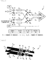
- FIG. 1 illustrates an overview of the communication system 1.
- the communication system 1 is applied to multipoint bus transmission.
- the communication system 1 includes two transmission devices TX1 and TX2 and one reception device RX.
- the communication system 1 further includes a transmission path P that couples the respective transmission devices TX1 and TX2 and the reception device RX to each other, for example, as illustrated in FIGs. 1, 2 , 3, and 4 .
- the communication system 1 transmits signals from the two transmission devices TX1 and TX2 to the one reception device RX via the transmission path P.
- the transmission path P is branched at a midpoint into three, and has branch points H p and H n .
- a transmission path P 1 that is one of branches couples the transmission device TX1 and the branch points H p and H n to each other.
- the transmission path P 1 includes differential signal lines (a pair of signal lines P 1p and P 1n ) that transmit a differential signal.
- the signal line P 1p is coupled to the branch point H p
- the signal line P 1n is coupled to the branch point H n .
- a terminator resistor R T /2 of the transmission device TX1 is provided for each of the signal lines P 1p and P 1n .
- a transmission path P 2 that is one of the branches couples the transmission device TX2 and the branch points H p and H n to each other.
- the transmission path P 2 includes differential signal lines (a pair of signal lines P 2p and P 2n ) that transmit a differential signal.
- the signal line P 2p is coupled to the branch point H p
- the signal line P 2n is coupled to the branch point H n .
- the terminator resistor R T /2 of the transmission device TX2 is provided for each of the signal lines P 2p and P 2n .
- a transmission path P 3 that is one of the branches couples the reception device RX and the branch points H p and H n to each other.
- the transmission path P 3 includes differential signal lines (a pair of signal lines P 3p and P 3n ) that transmit a differential signal.
- the signal line P 3p is coupled to the branch point H p
- the signal line P 3n is coupled to the branch point H n .
- the terminator resistor R T /2 of the reception device RX is provided for each of the signal lines P 3p and P 3 .
- the signal lines P 1p , P 2p , and P 3p are coupled to each other at the branch point H p .
- the signal line P 1n , P 2n , and P 3n are coupled to each other at the branch point H n .
- the transmission paths P 1 , P 2 , and P 3 are formed on a wiring substrate, for example.
- the transmission paths P 1 and P 3 are formed in a common layer on the wiring substrate, and the transmission path P 2 is formed in a layer different from the transmission paths P 1 and P 3 on the wiring substrate.
- the transmission paths P 1 and P 3 and the transmission path P 2 are electrically coupled to each other via the branch points H p and H n that each include a through hole.
- the transmission paths P 2 and P 3 may be formed in a common layer on the wiring substrate, and the transmission path P 1 may be formed in a layer different from the transmission paths P 2 and P 3 on the wiring substrate. Further, for example, as illustrated in FIG. 4 , the transmission paths P 2 and P 3 and the transmission path P 1 may be electrically coupled to each other via the branch points H p and H n that each include a through hole.
- Each of the signal lines P 1p , P 2p , and P 3p includes a resistor element R in proximity to the branch point H p . Further, each of the signal lines P 1n , P 2n , and P 3n also includes the resistor element R in proximity to the branch point H n .
- the resistor element R has a resistance value represented by the following expression (1), where a characteristic impedance of each of the signal lines P 1p , P 1n , P 2p , P 2n , P 3p , and P 3n is Z 0 , each of the terminator resistors for the respective signal lines P 1p , P 1n , P 2p , and P 2n of the respective transmission devices TX1 and TX2 is R T /2, and each of the terminator resistors for the respective signal lines P 3p and P 3n of the reception device RX is R T /2.
- R number of branches ⁇ 1 ⁇ Z 0 ⁇ R T / 2 / number of branches
- each of the signal lines P 1p , P 1n , P 2p , P 2n , P 3p , and P 3n has 50 ohms (Rs) as viewed from any port of the transmission devices TX1 and TX2 and the reception device RX, and is a transmission path achieving impedance matching.
- the respective resistor elements R are disposed as close to the branch points H p and H n as possible.
- the signal lines P 1p and P 1n are disposed to lay wiring patterns of the signal line P 1p and the signal line P 1n in as approximate a layout as possible.
- the signal lines P 2p and P 2n are disposed to lay wiring patterns of the signal line P 2p and the signal line P 2n in as approximate a layout as possible.
- the signal lines P 3p and P 3n are disposed to lay wiring patterns of the signal line P 3p and the signal line P 3n in as approximate a layout as possible.
- the respective signal lines P 1p , P 1n , P 2p , P 2n , P 3p , and P 3n are disposed to lay wiring patterns of different lanes in as approximate a layout as possible.
- the transmission path P is preferably configured to make characteristics of respective layers close to each other.
- use rates of the respective layers are preferably made uniform to less prone to cause a difference in characteristic of respective wiring lines included in one lane and a difference in characteristics between lanes.
- the transmission device TX1 In the communication system 1, in a case where the transmission device TX1 outputs a signal, for example, as illustrated in FIG. 1 , output of the transmission device TX2 is stopped, and further, the transmission device TX2 is differentially terminated. Similarly, in the communication system 1, in a case where the transmission device TX2 outputs a signal, output of the transmission device TX1 is stopped, and further, the transmission device TX1 is differentially terminated.
- the transmission devices TX1 and TX2 are set to one of signal output and differential termination in accordance with a control signal from outside.
- FIG. 5 illustrates an example of pass characteristics in the communication system 1.
- FIG. 6 illustrates an example of reflection characteristics in the communication system 1.
- FIG. 7 illustrates an example of an eye diagram in the communication system 1.
- a lower waveform of two waveforms is a result of pass characteristics as viewed from the transmission devices TX1 and TX2
- an upper waveform of the two waveforms is a result of pass characteristics as viewed from the reception device RX.
- a result of reflection characteristics as viewed from the transmission devices TX1 and TX2 and a result of reflection characteristics as viewed from the reception device RX are superimposed on each other.
- a signal level around 1 GHz is -5 dB. This means that a level of a passing signal is decreased to about 56% by insertion of the resistor element R.
- a signal level around 1 GHz is -15 dB. This means that a level of a reflected signal is decreased to about 18%.
- FIG. 7 an eye of the eye diagram is clearly open.
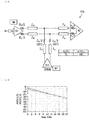
- FIG. 8 illustrates an overview of a communication system 100 according to a comparative example A.
- FIG. 9 illustrates an example of pass characteristics in the communication system 100.
- FIG. 10 illustrates an example of reflection characteristics in the communication system 100.
- FIG. 11 illustrates an example of an eye diagram in the communication system 100.
- the terminator resistor R T /2 of the transmission device TX1 is provided for each of the signal lines P 1p and P 1n
- the terminator resistor R T /2 of the reception device RX is provided for each of the signal lines P 3p and P 3n .
- the communication system 100 includes a transmission path using SSTL (Stub Series Termination Logic).
- an SST having a resistance value of Z 0 /2 is inserted in series in each of the signal lines P 2p and P 2n that are branched on a side where the transmission device TX2 serving as a stub is located. This eliminates impedance mismatching in a bus as viewed from the transmission device TX2.
- a signal level around 1 GHz is about -2 dB. This is because the resistor element R as in the present embodiment is not inserted, and the signal level is not decreased much.
- a signal level around 1 GHz is about -7 dB. This means that a half of an inputted signal is returned by reflection.
- an eye of the eye diagram is extremely small, as compared with the eye of the eye diagram in FIG. 7 . As can be seen from these factors, in the communication system 100, many noises are caused by reflection, and signals are difficult to pass.
- FIG. 12 illustrates an overview of a communication system 200 according to a comparative example B.
- FIG. 13 illustrates an example of pass characteristics in the communication system 200.
- FIG. 14 illustrates an example of reflection characteristics in the communication system 200.
- FIG. 15 illustrates an example of an eye diagram in the communication system 200.
- the terminator resistor R T /2 of the transmission device TX2 is provided for each of the signal lines P 2p and P 2n
- the terminator resistor R T /2 of the reception device RX is provided for each of the signal lines P 3p and P 3 .
- the communication system 200 includes a transmission path using SSTL.
- an SST having a resistance value of Z 0 /2 is inserted in series in each of the signal lines P 2p and P 2n that are branched on a side where the transmission device TX2 serving as a stub is located. This eliminates impedance mismatching in a bus as viewed from the transmission device TX2.
- a signal level around 1 GHz is about -2 dB. This is because the resistor element R as in the present embodiment is not inserted, and the signal level is not decreased much.
- a signal level around 1 GHz is about -2 dB. This means that most of an inputted signal is returned by reflection.
- FIG. 15 an eye of the eye diagram is hardly seen. As can be seen from these factors, in the communication system 200, many noises are caused by reflection, and signals are difficult to pass.
- FIG. 16 illustrates an overview of the communication system 200 according to a comparative example C.
- FIG. 17 illustrates an example of pass characteristics in a communication system 300.
- FIG. 18 illustrates an example of reflection characteristics in the communication system 300.
- FIG. 19 illustrates an example of an eye diagram in the communication system 300.
- the terminator resistor R T /2 of the transmission device TX1 is provided for each of the signal lines P 1p and P 1n
- the terminator resistor R T /2 of the transmission device TX2 is also provided for each of the signal lines P 2p and P 2n .
- the terminator resistor R T /2 of the reception device RX is also provided for each of the signal lines P 3p and P 3n .
- the communication system 300 includes a transmission path using SSTL. Specifically, in the communication system 300, an SST having a resistance value of Z 0 /2 is inserted in series in each of the signal lines P 2p and P 2n that are branched on a side where the transmission device TX2 serving as a stub is located. This eliminates impedance mismatching in a bus as viewed from the transmission device TX2.
- a signal level around 1 GHz is about -4 dB. This is because the resistor element R as in the present embodiment is not inserted, and the signal level is not decreased much.
- a signal level around 1 GHz is about -6 dB. This means that about a half of an inputted signal is returned by reflection.
- an eye of the eye diagram is seen to some extent. As can be seen from these factors, in the communication system 300, many noises are caused by reflection, and signals are difficult to pass.
- High-speed interface specifications such as C-PHY specification and D-PHY specification that have been developed by the MIPI alliance are applied in a case where image data from a plurality of cameras is transmitted to an application processor and the like.
- data transmission is point-to-point transmission; therefore, for example, there are many issues to be solved to support a plurality of cameras, such as limitations on the number of pins on an application processor side, an increase in size of a transmission path, and product design.
- Multipoint bus transmission shows promise for support of a plurality of cameras.
- waveform quality is greatly deteriorated by an influence of reflection and the like; therefore, the existing multipoint bus transmission is not suitable for high-speed transmission.
- many noises are caused by reflection, and signals are difficult to pass.
- the three-branched branch points H p and H n are provided in the transmission path P, and the resistor element R is provided for each of signal lines at the three-branched branch points H p and H n .
- the resistor element R is provided for each of signal lines at the three-branched branch points H p and H n .
- each of the resistor elements R provided in the transmission path P has a resistance value represented by the expression (1) described above. Accordingly, each of the signal lines P 1p , P 1n , P 2p , P 2n , P 3p , and P 3n has 50 ohms (Rs) as viewed from any port of the transmission devices TX1 and TX2 and the reception device RX, and is a transmission path achieving impedance matching. This makes it possible to achieve multipoint bus transmission suitable for high-speed transmission.
- a transmission device e.g., the transmission device TX2 that does not output a signal is differentially terminated. This makes it possible to reduce noise in the transmission path P, as compared with a case where the transmission device that does not output a signal becomes a released end. This makes it possible to achieve multipoint bus transmission suitable for high-speed transmission.
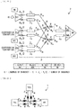
- FIG. 20 illustrates an overview of the communication system 2.
- the communication system 2 is applied to multipoint bus transmission.
- the communication system 2 includes three transmission devices TX1, TX2, and TX3, and one reception device RX.
- the communication system 2 further includes, for example, the transmission path P that couples the respective transmission devices TX1, TX2, and TX3 and the reception device RX to each other, for example, as illustrated in FIG. 20 .
- the communication system 2 transmits signals from the three transmission devices TX1, TX2, and TX3 to the one reception device RX via the transmission path P.
- the transmission path P is branched at a midpoint into four, and has the branch points H p and H n .
- the transmission path P 1 that is one of branches couples the transmission device TX1 and the branch points H p and H n to each other.
- the transmission path P 1 includes differential signal lines (a pair of signal lines P 1p and P 1n ) that transmit a differential signal.
- the signal line P 1p is coupled to the branch point H p
- the signal line P 1n is coupled to the branch point H n .
- the terminator resistor R T /2 of the transmission device TX1 is provided for each of the signal lines P 1p and P 1n .
- the transmission path P 2 that is one of the branches couples the transmission device TX2 and the branch points H p and H n to each other.
- the transmission path P 2 includes differential signal lines (a pair of signal lines P 2p and P 2n ) that transmit a differential signal.
- the signal line P 2p is coupled to the branch point H p
- the signal line P 2n is coupled to the branch point H n .
- the terminator resistor R T /2 of the transmission device TX2 is provided for each of the signal lines P 2p and P 2n .
- the transmission path P 3 that is one of the branches couples the reception device RX and the branch points H p and H n to each other.
- the transmission path P 3 includes differential signal lines (a pair of signal lines P 3p and P 3n ) that transmit a differential signal.
- the signal line P 3p is coupled to the branch point H p
- the signal line P 3n is coupled to the branch point H n .
- the terminator resistor R T /2 of the reception device RX is provided for each of the signal lines P 3p and P 3n .
- a transmission path P 4 that is one of the branches couples the transmission device TX3 and the branch points H p and H n to each other.
- the transmission path P 4 includes differential signal lines (a pair of signal lines P 4p and P 4n ) that transmit a differential signal.
- the signal line P 4p is coupled to the branch point H p
- the signal line P 4n is coupled to the branch point H n .
- the terminator resistor R T /2 of the transmission device TX3 is provided for each of the signal lines P 4p and P 4n .
- the signal lines P 1p , P 2p , P 3p , and P 4p are coupled to each other at the branch point H p .
- the signal lines P 1n , P 2n , P 3n , and P 4n are coupled to each other at the branch point H n .
- Each of the signal lines P 1p , P 2p , P 3p , and P 4p includes the resistor element R in proximity to the branch point H p . Further, each of the signal lines P 1n , P 2n , P 3n , and P 4n also includes the resistor element R in proximity to the branch point H n .
- the resistor element R has a resistance value represented by the expression (1) described above, where a characteristic impedance of each of the signal lines P 1p , P 1n , P 2p , P 2n , P 3p , P 3n , P 4p , and P 4n is Z 0 , a terminator resistor for each of the signal lines P 1p , P 1n , P 2p , P 2n , P 4p , and P 4n of the respective transmission devices TX1, TX2, and TX3 is R T /2, a terminator resistor for each of the signal lines P 3p and P 3n of the reception device RX is R T /2.
- each of the signal lines P 1p , P 1n , P 2p , P 2n , P 3p , P 3n , P 4p , and P 4n has 50 ohms (Rs) as viewed from any port of the transmission devices TX1, TX2, and TX3 and the reception device RX, and is a transmission path achieving impedance matching.
- the respective resistor elements R are disposed as close to the branch points H p and H n as possible.
- the signal lines P 1p and P 1n are disposed to lay wiring patterns of the signal line P 1p and the signal line P 1n in as approximate a layout as possible.
- the signal lines P 2p and P 2n are disposed to lay wiring patterns of the signal line P 2p and the signal line P 2n in as approximate a layout as possible.
- the signal lines P 3p and P 3n are disposed to lay wiring patterns of the signal line P 3p and the signal line P 3n in as approximate a layout as possible.
- the signal lines P 4p and P 4n are disposed to lay wiring patterns of the signal line P 4p and the signal line P 4n in as approximate a layout as possible.
- the respective signal lines P 1p , P 1n , P 2p , P 2n , P 3p , P 3n , P 4p , and P 4n are disposed to lay wiring patterns of different lanes in as approximate a layout as possible.
- one set of the four-branched branch points H p and H n is provided in the transmission path P, and the resistor element R is provided for each of signal lines at each set of the four-branched branch points H p and H n .
- the resistor element R is provided for each of signal lines at each set of the four-branched branch points H p and H n .
- each of the resistor elements R provided in the transmission path P has a resistance value represented by the expression (1) described above. Accordingly, each of the signal lines P 1p , P 1n , P 2p , P 2n , P 3p , P 3n , P 4p , and P 4n has 50 ohms (Rs) as viewed from any port of the transmission devices TX1, TX2, and TX3 and the reception device RX, and is a transmission path achieving impedance matching. This makes it possible to achieve multipoint bus transmission suitable for high-speed transmission.
- a transmission device e.g., the transmission devices TX2 and TX3 that does not output a signal is differentially terminated. This makes it possible to reduce noise in the transmission path P, as compared with a case where the transmission device that does not output a signal becomes a released end. This makes it possible to achieve multipoint bus transmission suitable for high-speed transmission.
- FIG. 21 illustrates an example of a mounting form of the three-branched communication system 1.
- the communication system 1 transmits signals from the two transmission devices TX1 and TX2 to the one reception device RX via the transmission path P.
- the respective resistor elements R are disposed in proximity to the branch points H p and H n .
- the signal line P 1p and the signal line P 2p are coupled to each other at the branch point H p .
- the signal line P 1n and the signal line P 2n are coupled to each other at the branch point H n .
- the signal line P 1p and the signal line P 3p are disposed in a common transmission path at the branch point H p .
- the signal line P 1n and the signal line P 3n are disposed in a common transmission path at the branch point H p .
- one set of the three-branched branch points H p and H n is provided in the transmission path P, and the resistor element R is provided for each of signal lines at each set of the three-branched branch points H p and H n .
- the resistor element R is provided for each of signal lines at each set of the three-branched branch points H p and H n .
- FIG. 22 illustrates an example of a mounting form of the four-branched communication system 2.
- the communication system 2 transmits signals from the three transmission devices TX1, TX2, and TX3 to the one reception device RX via the transmission path P.
- the three-branched branch points H p and H n are provided in two spots (a spot A and a spot B) of the transmission path P, and the resistor element R is provided for each of signal lines in each of the spots A and B.
- each of the resistor elements R has a resistance value in a case where the number of branches is three in the expression (1).
- the signal line P 1p and the signal line P 2p are coupled to each other at the branch point H p in the spot A.
- the signal line P 1n and signal line P 2n are coupled to each other at the branch point H n in the spot A.
- the signal line P 1p and a signal line P 5p are disposed in a common transmission path at the branch point H p in the spot A.
- the signal line P 1n and a signal line P 5n are disposed in a common transmission path at the branch point H n in the spot A.
- the signal line P 5p is a wiring line that electrically couples the signal line P 1p in the spot A and the signal line P 3p in the spot B to each other.
- the signal line P 5n is a wiring line that electrically couples the signal line P 1n in the spot A and the signal line P 3n in the spot B to each other.
- the signal line P 3p and the signal line P 4p are coupled to each other at the branch point H p in the spot B.
- the signal line P 3n and signal line P 4n are coupled to each other at the branch point H n in the spot B.
- the signal line P 3p and the signal line P 5p are disposed in a common transmission path at the branch point H p in the spot B.
- the signal line P 3n and the signal line P 5n are disposed in a common transmission path at the branch point H n in the spot B.
- two sets of the three-branched branch points H p and H n are provided in the transmission path P, and the resistor element R is provided for each of signal lines at each set of the three-branched branch points H p and H n .
- the resistor element R is provided for each of signal lines at each set of the three-branched branch points H p and H n .
- FIG. 23 illustrates an example of a mounting form of a five-branched communication system 3.
- the communication system 3 transmits signals from the four transmission devices TX1, TX2, TX3, and TX4 to the one reception device RX via the transmission path P.
- FIG. 23 corresponds to the four-branched communication system 2 in FIG. 22 that is newly provided with three branches in each of the signal line P 3p and the signal line P 4p .
- spot C a spot where three branches are newly provided.
- the resistor element FR is provided for each of signals lines.
- each of the resistor elements R has a resistance value (16.7 ohms) in a case where the number of branches is three in the expression (1).
- the signal line P 4p and a signal line P 6p are coupled to each other at the branch point H p in the spot C.
- the signal line P 4n and a signal line P 6n are coupled to each other at the branch point H n in the spot C.
- the signal line P 6p is one wiring line coupled to the transmission device TX4.
- the signal line P 6n is another wiring line coupled to the transmission device TX4.
- the signal line P 4p and a signal line P 7p are disposed in a common transmission path at the branch point H p in the spot C.
- the signal line P 4n and a signal line P 7n are disposed in a common transmission path at the branch point H n in the spot C.
- the signal line P 7p is one wiring line coupled to the transmission device TX3.
- the signal line P 7n is another wiring line coupled to the transmission device TX3.
- the transmission device TX3 outputs a signal
- the transmission devices TX1, X2 and X4 are stopped, and further, the transmission devices TX1, X2, and X4 are differentially terminated.
- the transmission device TX4 outputs a signal
- output of the transmission devices TX1, X2 and X3 is stopped, and further, the transmission devices TX1, X2, and X3 are differentially terminated.
- the transmission devices TX1, TX2, TX3, and TX4 are set to one of signal output and differential termination in accordance with a control signal from outside.
- two sets of the three-branched branch points H p and H n are provided in the transmission path P, and further, one set of the three-branched branch points H p and H n is provided in a pair of signal lines branched at one of the sets of the branch points H p and H n from a main transmission path that couples the transmission device TX1 and the reception device RX to each other.
- the resistor element R is provided for each of signal lines at each set of the three-branched branch points H p and H n .
- FIG. 24 illustrates a modification example of the communication system 1.
- the communication system 1 illustrated in FIG. 24 corresponds to the communication system 1 according to the embodiment described above from which the respective resistor elements R provided close to the reception device RX at the branch points H p and H n are omitted.
- each of the signal lines P 1p , P 1n , P 2p , P 2n , P 3p , and P 3n has 50 ohms (R S-fromTX ) as viewed from any port of the transmission devices TX1 and TX2, and has 35.35 ohms(R S-fromRX ) as viewed from a port of the reception device RX.
- FIG. 25 illustrates an example of pass characteristics in the communication system 1 illustrated in FIG. 24 .
- FIG. 26 illustrates an example of reflection characteristics in the communication system 1 illustrated in FIG. 24 .
- FIG. 27 illustrates an example of an eye diagram in the communication system 1 illustrated in FIG. 24 .
- a lower waveform of two waveforms is a result of pass characteristics as viewed from the transmission devices TX1 and TX2, and an upper waveform of the two waveforms is a result of pass characteristics as viewed from the reception device RX.
- FIG. 25 illustrates an example of pass characteristics in the communication system 1 illustrated in FIG. 24 .
- FIG. 26 illustrates an example of reflection characteristics in the communication system 1 illustrated in FIG. 24 .
- FIG. 27 illustrates an example of an eye diagram in the communication system 1 illustrated in FIG. 24 .
- a lower waveform of two waveforms is a result of pass characteristics as viewed from the transmission devices TX1 and TX2
- an upper waveform of the two waveforms is a result
- a result of reflection characteristics as viewed from the transmission devices TX1 and TX2 and a result of reflection characteristics as viewed from the reception device RX are not superimposed on each other, and the reflection characteristics as viewed from the transmission devices TX1 and TX2 is superior to the reflection characteristics as viewed from the reception device RX.
- a signal level around 1 GHz is -3 dB, which is slightly improved, as compared with the signal level in FIG. 5 .
- the respective resistor elements R provided close to the reception device RX at the branch points H p and H n are omitted, which prevents voltage division by the respective resistor elements R provided close to the reception device RX.
- a signal level around 1 GHz is -18 dB, and in the reflection characteristics as viewed from the reception device RX, a signal level around 1 GHz is -10 dB.
- FIG. 27 an eye of the eye diagram is clearly open.
- the present modification example omitting the respective resistor elements R provided close to the reception device RX at the branch points H, and H n makes it possible to improve a signal level inputted to the reception device RX. Accordingly, the present modification example is resistant to noise by an improved amount of the signal level, which makes it possible to achieve multipoint bus transmission suitable for high-speed transmission.
- FIG. 28 illustrates an overview of the communication system 4.
- the communication system 4 is applied to multipoint bus transmission.
- the communication system 4 includes two transmission devices TX1 and TX2 and one reception device RX.
- the communication system 4 further includes the transmission path P that couples the respective transmission devices TX1 and TX2 and the reception device RX to each other, for example, as illustrated in FIG. 28 .
- the communication system 4 transmits signals from the two transmission devices TX1 and TX2 to the one reception device RX via the transmission path P.
- the transmission path P is branched at a midpoint into three, and has branch points H 1 , H 2 , and H 3 .
- the transmission path P 1 that is one of branches couples the transmission device TX1 and the branch points H 1 , H 2 , and H 3 to each other.
- the transmission path P 1 includes three signal lines P 11 , P 12 , and P 13 that transmit a set of three signals.
- the signal line P 11 is coupled to the branch point H 1 .
- the signal line P 12 is coupled to the branch point H 2 .
- the signal line P 13 is coupled to the branch point H 3 .
- the transmission path P 2 that is one of the branches couples the transmission device TX2 and the branch points H 1 , H 2 , and H 3 to each other.
- the transmission path P 2 includes three signal lines P 21 , P 22 , and P 23 that transmit a set of three signals.
- the signal line P 21 is coupled to the branch point H 1 .
- the signal line P 22 is coupled to the branch point H 2 .
- the signal line P 23 is coupled to the branch point H 3 .
- the transmission path P 3 that is one of the branches couples the transmission device TX3 and the branch points H 1 , H 2 , and H 3 to each other.
- the transmission path P 3 includes three signal lines P 31 , P 32 , and P 33 that transmit a set of three signals.
- the signal line P 31 is coupled to the branch point H 1 .
- the signal line P 32 is coupled to the branch point H 2 .
- the signal line P 33 is coupled to the branch point H 3 .
- Each of the signal lines P 11 , P 21 , and P 31 includes the resistor element R in proximity to the branch point H 1 .
- Each of the signal lines P 12 , P 22 , and P 32 includes the resistor element R in proximity to the branch point H 2 .
- Each of the signal lines P 13 , P 23 , and P 33 includes the resistor element R in proximity to the branch point H 3
- the resistor element R has a resistance value represented by the expression (1) described above, where a characteristic impedance of each of the signal lines P 11 , P 21 , P 31 , P 12 , P 22 , P 32 , P 13 , P 23 , and P 33 is Z 0 , a terminator resistor for each of the signal lines P 11 , P 21 , P 12 , P 22 , P 13 , and P 23 of the respective transmission devices TX1 and TX2 is R T /2, a terminator resistor for each of the signal lines P 31 , P 32 , and P 33 of the reception device RX is R T /2.
- each of the signal lines P 11 , P 21 , P 31 , P 12 , P 22 , P 32 , P 13 , P 23 , and P 33 has 50 ohms (Rs) as viewed from any port of the transmission devices TX1 and TX2 and the reception device RX, and is a transmission path achieving impedance matching.
- the transmission device TX1 In the communication system 4, in a case where the transmission device TX1 outputs a signal, output of the transmission device TX2 is stopped, and further, the transmission device TX2 is differentially terminated. Similarly, in the communication system 4, in a case where the transmission device TX2 outputs a signal, output of the transmission device TX1 is stopped, and further, the transmission device TX1 is differentially terminated.
- the transmission devices TX1 and TX2 are set to one of signal output and differential termination in accordance with a control signal from outside.
- the three-branched branch points H 1 , H 2 , and H 3 are provided in the transmission path P, and the resistor element R is provided for each of signal lines at the three-branched branch points H 1 , H 2 , and H 3 .
- the resistor element R is provided for each of signal lines at the three-branched branch points H 1 , H 2 , and H 3 .
- each of the resistor elements R provided in the transmission path P has a resistance value represented by the expression (1) described above. Accordingly, each of the signal lines P 11 , P 21 , P 31 , P 12 , P 22 , P 32 , P 13 , P 23 , and P 33 has 50 ohms (Rs) as viewed from any port of the transmission devices TX1 and TX2 and the reception device RX, and is a transmission path achieving impedance matching. This makes it possible to achieve multipoint bus transmission suitable for high-speed transmission.
- a transmission device e.g., the transmission device TX2 that does not output a signal is differentially terminated. This makes it possible to reduce noise in the transmission path P, as compared with a case where the transmission device that does not output a signal becomes a released end. This makes it possible to achieve multipoint bus transmission suitable for high-speed transmission.
- a portion including the branch points H p and H n or the branch points H 1 , H 2 , and H 3 , and the respective element resistors R may include a transmitter such as an IC (Integrated Circuit) and a module.
- the transmission path P may include a transmitter 10, for example, as illustrated in FIG. 29 .
- the transmitter 10 includes, for example, the branch points H p and H n , and six resistor elements provided in proximity to the branch points H p and H n in the respective signal lines P 1p , P 1n , P 2p , P 2n , P 3p , and P 3n .
- the transmitter 10 further includes, for example, six coupling terminals T 1p , T 1n , T 2p , T 2n , T 3p , and T 3n coupled to ends on a side opposite to the branch points H p and H n of the respective signal line P 1p , P 1n , P 2p , P 2n , P 3p , and P 3n .
- the transmission path P may include a transmitter 20, for example, as illustrated in FIG. 30 .
- the transmitter 20 includes, for example, the branch points H p and H n , and eight resistor elements provided in proximity to the branch points H p and H n in the respective signal lines P 1p , P 1n , P 2p , P 2n , P 3p , P 3n , P 4p , and P 4n .
- the transmitter 20 further includes, for example, eight coupling terminals T 1p , T 1n , T 2p , T 2n , T 3p , T 3n , T 4p , and T 4n coupled to ends on a side opposite to the branch points H p and H n of the respective signal line P 1p , P 1n , P 2p , P 2n , P 3p , P 3n , P 4p , and P 4n .
- the communication system 1 in FIG. 21 may include a transmitter 30, for example, as illustrated in FIG. 31 .
- the transmitter 30 includes, for example, the branch points H p and H n , and six resistor elements provided in proximity to the branch points H p and H n in the respective signal lines P 1p , P 1n , P 2p , P 2n , P 3p , and P 3n .
- the transmitter 30 further includes, for example, six coupling terminals T 1p , T 1n , T 2p , T 2n , T 3p , and T 3n coupled to ends on a side opposite to the branch points H p and H n in the respective signal line P 1p , P 1n , P 2p , P 2n , P 3p , and P 3n .
- each of the A spot and the B spot of the transmission path P may include the transmitter 30, for example, as illustrated in FIG. 31 .
- each of the A spot, the B spot, and the C spot of the transmission path P may include the transmitter 30, for example, as illustrated in FIG. 31 .
- the transmission path P may include a transmitter 40, for example, as illustrated in FIG. 32 .
- the transmitter 40 includes, for example, the branch points H p and H n , and four resistor elements R provided in proximity to the branch points H p and H n in the respective signal lines P 1p , P 1n , P 2p , and P 2n .
- the transmitter 10 further includes, for example, six coupling terminals T 1p , T 1n , T 2p , T 2n , T 3p , and T 3n coupled to ends on a side opposite to the branch points H p and H n of the respective signal line P 1p , P 1n , P 2p , P 2n , P 3p , and P 3n .
- the element resistor R is not provided for each of the signal lines P 3p and P 3n .
- the transmission path P may include a transmitter 50, for example, as illustrated in FIG. 33 .
- the transmitter 50 includes, for example, the branch points H 1 , H 2 , and H 3 , and nine resistor elements R provided in proximity to the branch points H 1 , H 2 , and H 3 in the respective signal lines P 11 , P 12 , P 13 , P 21 , P 22 , P 23 , P 31 , P 32 , and P 33 .
- the transmitter 50 further includes, for example, nine coupling terminals T 11 , T 12 , T 13 , T 21 , T 22 , T 23 , T 31 , T 32 , and T 33 coupled to ends on a side opposite to the branch points H 1 , H 2 , and H 3 of the respective signal line signal line P 11 , P 12 , P 13 , P 21 , P 22 , P 23 , P 31 , P 32 , and P 33 .
- a portion including the branch points H p and H n or the branch points H 1 , H 2 , and H 3 , and the respective element resistors R may include a transmitter such as an IC (Integrated Circuit) and a module. This makes it possible to easily construct the transmission path P.
- IC Integrated Circuit
- a switch element may be provided.
- the switch element changes the number of branches at the branch points H p and H n or the branch points H 1 , H 2 , and H 3 .
- the transmitter 10 in FIG. 29 may include a switch element SW1 that changes the number of branches at the branch point H p and a switch element SW2 that changes the number of branches at the branch point H n , for example, as illustrated in FIG. 34 .
- the switch element SW1 includes a switch that performs coupling and decoupling between the branch point H p and the resistor element R in the signal line P 1p , a switch that performs coupling and decoupling between the branch point H p and the resistor element R in the signal line P 2p , and a wiring line that couples the branch point H p and the signal line P 3p to each other.
- the switch element SW1 turns on and off the two internal switches in accordance with a control signal from outside.
- the switch element SW1 couples, for example, at least one of the signal line P 1p or P 2p and the signal line P 3p to each other in accordance with a control signal from outside.
- the switch element SW2 includes a switch that performs coupling and decoupling between the branch point H n and the resistor element R in the signal line P 1n , a switch that performs coupling and decoupling between the branch point H n and the resistor element R in the signal line P 2n , and a wiring line that couples the branch point H n and the signal line P 3n to each other.
- the switch element SW2 turns on and off the two internal switches in accordance with a control signal from outside.
- the switch element SW2 couples, for example, at least one of the signal line P 1n or P 2n and the signal line P 3n to each other in accordance with a control signal from outside.
- the transmitter 20 in FIG. 30 may include a switch element SW3 that changes the number of branches at the branch point H p and a switch element SW4 that changes the number of branches at the branch point H n , for example, as illustrated in FIG. 35 .
- the switch element SW3 includes a switch that performs coupling and decoupling between the branch point H p and the resistor element R in the signal line P 1p , a switch that performs coupling and decoupling between the branch point H p and the resistor element R in the signal line P 2p , a switch that performs coupling and decoupling between the branch point H p and the resistor element R in the signal line P 3p , and a wiring line that couples the branch point H p and the signal line P 4p to each other.
- the switch element SW3 turns on and off the three internal switches in accordance with a control signal from outside.
- the switch element SW3 couples, for example, at least one of the signal line P 1p , P 2p , or P 4p and the signal line P 3p to each other in accordance with a control signal from outside.
- the switch element SW4 includes a switch that performs coupling and decoupling between the branch point H n and the resistor element R in the signal line P 1n , a switch that performs coupling and decoupling between the branch point H n and the resistor element R in the signal line P 2n , a switch that performs coupling and decoupling between the branch point H n and the resistor element R in the signal line P 3n , and a wiring line that couples the branch point H n and the signal line P 4n to each other.
- the switch element SW4 turns on and off the three internal switches in accordance with a control signal from outside.
- the switch element SW4 couples, for example, at least one of the signal line P 1n , P 2n , or P 4n and the signal line P 3n to each other in accordance with a control signal from outside.
- the transmitter 30 in FIG. 31 may include a switch element SW5 that changes the number of branches at the branch point H p and a switch element SW6 that changes the number of branches at the branch point H n , for example, as illustrated in FIG. 36 .
- the switch element SW5 includes a switch that performs coupling and decoupling between the branch point H p and the resistor element R in the signal line P 1p , a switch that performs coupling and decoupling between the branch point H p and the resistor element R in the signal line P 2p , and a wiring line that couples the branch point H p and the signal line P 3p to each other.
- the switch element SW5 turns on and off the two internal switches in accordance with a control signal from outside.
- the switch element SW5 couples, for example, at least one of the signal line P 1p or P 2p and the signal line P 3p to each other in accordance with a control signal from outside.
- the switch element SW6 includes a switch that performs coupling and decoupling between the branch point H n and the resistor element R in the signal line P 1n , a switch that performs coupling and decoupling between the branch point H n and the resistor element R in the signal line P 2n , and a wiring line that couples the branch point H n and the signal line P 3n to each other.
- the switch element SW6 turns on and off the two internal switches in accordance with a control signal from outside.
- the switch element SW6 couples, for example, at least one of the signal line P 1n or P 2n and the signal line P 3n to each other in accordance with a control signal from outside.
- the transmitter 40 in FIG. 32 may include a switch element SW7 that changes the number of branches at the branch point H p and a switch element SW8 that changes the number of branches at the branch point H n , for example, as illustrated in FIG. 37 .
- the switch element SW7 includes a switch that performs coupling and decoupling between the branch point H p and the resistor element R in the signal line P 1p , a switch that performs coupling and decoupling between the branch point H p and the resistor element R in the signal line P 2p , and a wiring line that couples the branch point H p and the signal line P 3p to each other.
- the switch element SW7 turns on and off the two internal switches in accordance with a control signal from outside.
- the switch element SW7 couples, for example, at least one of the signal line P 1p or P 2p and the signal line P 3p to each other in accordance with a control signal from outside.
- the switch element SW8 includes a switch that performs coupling and decoupling between the branch point H n and the resistor element R in the signal line P 1n , a switch that performs coupling and decoupling between the branch point H n and the resistor element R in the signal line P 2n , and a wiring line that couples the branch point H n and the signal line P 3n to each other.
- the switch element SW8 turns on and off the two internal switches in accordance with a control signal from outside.
- the switch element SW8 couples, for example, at least one of the signal line P 1n or P 2n and the signal line P 3n to each other in accordance with a control signal from outside.
- the transmitter 50 in FIG. 33 may include a switch element SW9 that changes the number of branches at the branch point H 1 , a switch element SW10 that changes the number of branches at the branch point H 2 , and a switch element SW11 that changes the number of branches at the branch point H 3 for example, as illustrated in FIG. 38 .
- the switch element SW9 includes a switch that performs coupling and decoupling between the branch point H 1 and the resistor element R in the signal line P 11 , a switch that performs coupling and decoupling between the branch point H 1 and the resistor element R in the signal line P 21 , and a wiring line that couples the branch point H 1 and the resistor element R in the signal line P 31 to each other.
- the switch element SW9 turns on and off the two internal switches in accordance with a control signal from outside.
- the switch element SW9 couples, for example, at least one of the signal line P 11 or P 21 and the signal line P 31 to each other in accordance with a control signal from outside.
- the switch element SW10 includes a switch that performs coupling and decoupling between the branch point H 2 and the resistor element R in the signal line P 12 , a switch that performs coupling and decoupling between the branch point H 2 and the resistor element R in the signal line P 22 , and a wiring line that couples the branch point H 2 and the resistor element R in the signal line P 32 to each other.
- the switch element SW10 turns on and off the two internal switches in accordance with a control signal from outside.
- the switch element SW10 couples, for example, at least one of the signal line P 12 or P 22 and the signal line P 32 to each other in accordance with a control signal from outside.
- the switch element SW11 includes a switch that performs coupling and decoupling between the branch point H 3 and the resistor element R in the signal line P 13 , a switch that performs coupling and decoupling between the branch point H 3 and the resistor element R in the signal line P 23 , and a wiring line that couples the branch point H 3 and the resistor element R in the signal line P 33 to each other.
- the switch element SW10 turns on and off the two internal switches in accordance with a control signal from outside.
- the switch element SW11 couples, for example, at least one of the signal line P 13 or P 23 and the signal line P 33 to each other in accordance with a control signal from outside.
- the switch element that changes the number of branches at the branch point H p and H n or the branch point H 1 , H 2 , and H 3 is provided, which makes it possible to easily change the transmission path P in accordance with a purpose.
- each of the resistor elements R may include a variable resistor element having a resistance value variable in accordance with a control signal from outside.
- the resistance value of each of the resistor elements R is changed in synchronization with timing of switching between signal output and termination, for example. In such a case, it is possible to easily adjust the transmission path P in accordance with a purpose.
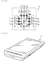
- FIG. 39 illustrates an appearance of a smartphone 5 (a multifunctional mobile phone) to which any of the communication systems 1 to 4 according to the respective embodiments and the modification examples thereof described above is applied.
- Various devices are mounted in the smartphone 5. Any of the communication systems 1 to 4 according to the respective embodiments and the modification examples thereof described above is applied to a communication system in which data are exchanged among these devices.
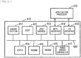
- FIG. 40 illustrates a configuration example of an application processor 310 to be used in the smartphone 5.
- the application processor 310 includes a CPU (Central Processing Unit) 311, a memory controller 312, a power source controller 313, an external interface 314, an MIPI interface 315, a GPU (Gaphics Processing Unit) 316, a media processor 317, a display controller 318, and an MIPI interface 319.
- the CPU 311, the memory controller 312, the power source controller 313, the external interface 314, the MIPI interface 315, the GPU 316, the media processor 317, and the display controller 318 are each coupled to a system bus 320 to allow for data exchange with one another via the system bus 320.
- the CPU 311 processes various pieces of information handled in the smartphone 5 in accordance with a program.
- the memory controller 312 controls a memory 501 to be used in a case where the CPU 311 performs information processing.
- the power source controller 313 controls a power source of the smartphone 5.
- the external interface 314 is an interface for communication with external devices.
- the external interface 314 is coupled to a wireless communication section 502.
- the wireless communication section 502 performs wireless communication with mobile phone base stations.
- the wireless communication section 502 includes, for example, a baseband section, an RF (radio frequency) front end section, and the like.
- the MIPI interface 315 receives an image signal from an image sensor 410.
- an image sensor 410 For example, any of the communication systems 1 to 4 according to the respective embodiments and the modification examples thereof described above is applied to a communication system between the MIPI interface 315 and the image sensor 410.
- the image sensor 410 acquires an image, and includes, for example, a CMOS sensor.
- the GPU 316 performs image processing.
- the media processor 317 processes information such as voice, characters, and graphics.
- the display controller 318 controls a display 504 via the MIPI interface 319.
- the MIPI interface 319 transmits an image signal to the display 504.
- the image signal for example, a signal such as a YUV-format signal and an RGB-format signal is usable.
- a signal such as a YUV-format signal and an RGB-format signal is usable.
- any of the communication systems 1 to 4 according to the respective embodiments and the modification examples thereof described above is applied to a communication system between the MIPI interface 319 and the display 504.
- FIG. 41 illustrates a configuration example of the image sensor 410.
- the image sensor 410 includes a sensor section 411, an ISP (Image Signal Processor) 412, a JPEG (Joint Photographic Experts Group) encoder 413, a CPU 414, a RAM (Random Access Memorr) 415, a ROM (Read Only Memory) 416, a power source controller 417, an I 2 C (Inter-Integrated Circuit) interface 418, and an MIPI interface 419.
- these respective blocks are coupled to a system bus 420 to allow for data exchange with one another via the system bus 420.
- the sensor section 411 acquires an image, and includes, for example, a CMOS sensor.
- the ISP 412 performs predetermined processing on the image acquired by the sensor section 411.
- the JPEG encoder 413 encodes the image processed by the ISP 412 to generate a JPEG-format image.
- the CPU 414 controls respective blocks of the image sensor 410 in accordance with a program.
- the RAM 415 is a memory to be used in a case where the CPU 414 performs information processing.
- the ROM 416 stores a program to be executed in the CPU 414.
- the power source controller 417 controls a power source of the image sensor 410.
- the I 2 C interface 418 receives a control signal from the application processor 310.
- the image sensor 410 also receives a clock signal from the application processor 310, in addition to the control signal.
- the image sensor 410 is configured to be operable on the basis of clock signals with various frequencies.
- the MIPI interface 419 transmits an image signal to the application processor 310.
- the image signal for example, a signal such as a YUV-format signal and an RGB-format signal is usable.
- a signal such as a YUV-format signal and an RGB-format signal is usable.
- any of the communication systems 1 to 4 according to the respective embodiments and the modification examples thereof described above is applied to a communication system between the MIPI interface 419 and the application processor 310.
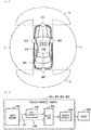
- FIG. 42 and FIG. 43 each illustrate a configuration example of a vehicle-mounted camera as an application example to an imaging device.
- FIG. 42 illustrates an installation example of the vehicle-mounted camera
- FIG. 43 illustrates an internal configuration example of the vehicle-mounted camera.
- vehicle-mounted cameras 401, 402, 403, and 404 are respectively mounted on the front (front), left, right, and rear (rear) of a vehicle 301, as illustrated in FIG. 42 .
- the vehicle-mounted cameras 401 to 404 are each coupled to an ECU (Electrical Control Unit) 302 via an in-vehicle network.
- ECU Electronic Control Unit
- An image capturing angle of the vehicle-mounted camera 401 mounted on the front of the vehicle 301 is within a range indicated by "a” in FIG. 42 , for example.
- An image capturing angle of the vehicle-mounted camera 402 is within a range indicated by "b” in FIG. 42 , for example.
- An image capturing angle of the vehicle-mounted camera 403 is within a range indicated by "c” in FIG. 42 , for example.
- An image capturing angle of the vehicle-mounted camera 404 is within a range indicated by "d” in FIG. 42 , for example.
- Each of the vehicle-mounted cameras 401 to 404 outputs a captured image to the ECU 302. This consequently makes it possible to capture a 360-degree (omnidirectional) image on the front, right, left, and rear of the vehicle 301 in the ECU 302.
- each of the vehicle-mounted cameras 401 to 404 includes an image sensor 431, a DSP (Digital Signal Processing) circuit 432, a selector 433, and a SerDes (SERializer/DESerializer) circuit 434, as illustrated in FIG. 43 .
- DSP Digital Signal Processing
- selector 433 selector 433
- SerDes SerDes
- the DSP circuit 432 performs various kinds of image signal processing on an imaging signal outputted from the image sensor 431.
- the SerDes circuit 434 performs serial-parallel conversion of a signal, and includes, for example, a vehicle-mounted interface chip such as FPD-Link III.
- the selector 433 selects whether to output the imaging signal outputted from the image sensor 431 via the DSP circuit 432 or not via the DSP circuit 432.
- any of the communication systems 1 to 4 according to the respective embodiments and the modification examples thereof described above is applicable to, for example, a coupling interface 441 between the image sensor 431 and the DSP circuit 432.
- any of the communication systems 1 to 4 according to the respective embodiments and the modification examples thereof described above is applicable to, for example, a coupling interface 442 between the image sensor 431 and the selector 433.
- the present disclosure may have the following configurations.
Landscapes
- Engineering & Computer Science (AREA)
- Computer Networks & Wireless Communication (AREA)
- Signal Processing (AREA)
- Power Engineering (AREA)
- Dc Digital Transmission (AREA)
- Cable Transmission Systems, Equalization Of Radio And Reduction Of Echo (AREA)
Abstract
Description
- The present disclosure relates to a communication system and a transmitter that are applied to transmission of a signal.
- In recent years, drones, wearable devices, automobiles, and the like equipped with a plurality of cameras are rapidly increasing. High-speed interface specifications such as C-PHY specification and D-PHY specification that have been developed by the MIPI (Mobile Industry Processor Interface) alliance are applied in a case where image data from a plurality of cameras is transmitted to an application processor and the like. PTL 1 proposes a technology for signal transmission in the D-PHY specification.
- PTL 1: Japanese Unexamined Patent Application Publication No.
2017-195500 - Incidentally, in the MIPI, data transmission is point-to-point transmission; therefore, for example, there are many issues to be solved to support a plurality of cameras, such as limitations on the number of pins on an application processor side, an increase in size of a transmission path, and product design. Multipoint bus transmission shows promise for support of a plurality of cameras. However, in existing multipoint bus transmission, waveform quality is greatly deteriorated by an influence of reflection and the like; therefore, the existing multipoint bus transmission is not suitable for high-speed transmission. It is therefore desirable to provide a communication system and a transmitter that make it possible to achieve multipoint bus transmission suitable for high-speed transmission.
- A communication system according to an embodiment of the present disclosure is a communication system that transmits a signal from a plurality of transmission devices to one reception device via a transmission path. In the communication system, the transmission path includes a branch point at a midpoint, includes a plurality of first signal lines that couples the transmission devices and the branch point to each other, and further includes a second signal line that couples the branch point and the reception device to each other. Of the plurality of first signal lines or the second signal line, at least the plurality of first signal lines has a resistor element in proximity to the branch point.
- A transmitter according to an embodiment of the present disclosure is a transmitter to be used for a communication system that transmits a signal from a plurality of transmission devices to one reception device. The transmitter includes: a branch point; a plurality of first signal lines that couples the transmission devices and the branch point to each other; a second signal line that couples the branch point and the reception device to each other; and a plurality of resistor elements provided in proximity to the branch point in at least the plurality of first signal lines of the plurality of first signal lines or the second signal line.
-
- [
FIG. 1] FIG. 1 is a diagram illustrating an overview of a communication system according to a first embodiment of the present disclosure. - [
FIG. 2] FIG. 2 is a diagram illustrating an example of a configuration of a transmission path in the communication system inFIG. 1 . - [
FIG. 3] FIG. 3 is a diagram illustrating an example of the configuration of the transmission path in the communication system inFIG. 1 . - [
FIG. 4] FIG. 4 is a diagram illustrating an example of the configuration of the transmission path in the communication system inFIG. 1 . - [
FIG. 5] FIG. 5 is a diagram illustrating an example of pass characteristics in the communication system inFIG. 1 . - [
FIG. 6] FIG. 6 is a diagram illustrating an example of reflection characteristics in the communication system inFIG. 1 . - [
FIG. 7] FIG. 7 is a diagram illustrating an example of an eye diagram in the communication system inFIG. 1 . - [
FIG. 8] FIG. 8 is a diagram illustrating an overview of a communication system according to a comparative example A. - [
FIG. 9] FIG. 9 is a diagram illustrating an example of pass characteristics in the communication system inFIG. 8 . - [
FIG. 10] FIG. 10 is a diagram illustrating an example of reflection characteristics in the communication system inFIG. 8 . - [
FIG. 11] FIG. 11 is a diagram illustrating an example of an eye diagram in the communication system inFIG. 8 . - [
FIG. 12] FIG. 12 is a diagram illustrating an overview of a communication system according to a comparative example B. - [
FIG. 13] FIG. 13 is a diagram illustrating an example of pass characteristics in the communication system inFIG. 12 . - [
FIG. 14] FIG. 14 is a diagram illustrating an example of reflection characteristics in the communication system inFIG. 12 . - [
FIG. 15] FIG. 15 is a diagram illustrating an example of an eye diagram in the communication system inFIG. 12 . - [
FIG. 16] FIG. 16 is a diagram illustrating an overview of a communication system according to a comparative example C. - [
FIG. 17] FIG. 17 is a diagram illustrating an example of pass characteristics in the communication system inFIG. 16 . - [
FIG. 18] FIG. 18 is a diagram illustrating an example of reflection characteristics in the communication system inFIG. 16 . - [
FIG. 19] FIG. 19 is a diagram illustrating an example of an eye diagram in the communication system inFIG. 16 . - [
FIG. 20] FIG. 20 is a diagram illustrating an overview of a communication system according to a second embodiment of the present disclosure. - [
FIG. 21] FIG. 21 is a diagram illustrating an example of a mounting form of a three-branched communication system. - [
FIG. 22] FIG. 22 is a diagram illustrating an example of a mounting form of a four-branched communication system. - [
FIG. 23] FIG. 23 is a diagram illustrating an example of a mounting form of a five-branched communication system. - [
FIG. 24] FIG. 24 is a diagram illustrating a modification example of the communication system inFIG. 1 . - [
FIG. 25] FIG. 25 is a diagram illustrating an example of pass characteristics in the communication system inFIG. 24 . - [
FIG. 26] FIG. 26 is a diagram illustrating an example of reflection characteristics in the communication system inFIG. 24 . - [
FIG. 27] FIG. 27 is a diagram illustrating an example of an eye diagram in the communication system inFIG. 24 . - [
FIG. 28] FIG. 28 is a diagram illustrating an overview of a communication system according to a third embodiment of the present disclosure. - [
FIG. 29] FIG. 29 is a diagram illustrating an example of the transmission path in the communication system inFIG. 1 . - [
FIG. 30] FIG. 30 is a diagram illustrating an example of a transmission path in the communication system inFIG. 20 . - [
FIG. 31] FIG. 31 is a diagram illustrating an example of a transmission path in the communication system inFIG. 21 . - [
FIG. 32] FIG. 32 is a diagram illustrating an example of a transmission path in the communication system inFIG. 24 . - [
FIG. 33] FIG. 33 is a diagram illustrating an example of a transmission path in the communication system inFIG. 28 . - [
FIG. 34] FIG. 34 is a diagram illustrating an example of the transmission path in the communication system inFIG. 29 . - [
FIG. 35] FIG. 35 is a diagram illustrating an example of the transmission path in the communication system inFIG. 30 . - [
FIG. 36] FIG. 36 is a diagram illustrating an example of the transmission path in the communication system inFIG. 31 . - [
FIG. 37] FIG. 37 is a diagram illustrating an example of the transmission path in the communication system inFIG. 32 . - [
FIG. 38] FIG. 38 is a diagram illustrating an example of the transmission path in the communication system inFIG. 33 . - [
FIG. 39] FIG. 39 is a perspective view of an appearance configuration of a smartphone to which the communication system according to any of the respective embodiments and modification examples thereof described above is applied. - [
FIG. 40] FIG. 40 is a block diagram illustrating a configuration example of an application processor to which the communication system according to any of the respective embodiments and modification examples thereof described above is applied. - [
FIG. 41] FIG. 41 is a block diagram illustrating a configuration example of an image sensor to which the communication system according to any of the respective embodiments and modification examples thereof described above is applied. - [
FIG. 42] FIG. 42 is a diagram illustrating an installation example of a vehicle-mounted camera to which the communication system according to any of the respective embodiments and modification examples thereof described above is applied. - [
FIG. 43] FIG. 43 is a diagram illustrating a configuration example in which the communication system according to any of the respective embodiments and modification examples thereof described above is applied to the vehicle-mounted camera. - Hereinafter, some embodiments of the present disclosure are described in detail with reference to the drawings. It should be noted that the description is given in the following order.
- 1. First Embodiment (communication system)
- 2. Second Embodiment (communication system)
- 3. Modification Example Common to First and Second Embodiments (communication system)
- 4. Third Embodiment (communication system)
- 5. Modification Example Common to First to Third Embodiments and Modification Examples Thereof (communication system)
- 6. Application Examples (smartphone, application processor, image sensor, and vehicle-mounted camera)
- Description is given of a communication system 1 according to a first embodiment of the present disclosure.
FIG. 1 illustrates an overview of the communication system 1. The communication system 1 is applied to multipoint bus transmission. The communication system 1 includes two transmission devices TX1 and TX2 and one reception device RX. The communication system 1 further includes a transmission path P that couples the respective transmission devices TX1 and TX2 and the reception device RX to each other, for example, as illustrated inFIGs. 1, 2 ,3, and 4 . The communication system 1 transmits signals from the two transmission devices TX1 and TX2 to the one reception device RX via the transmission path P. - The transmission path P is branched at a midpoint into three, and has branch points Hp and Hn. A transmission path P1 that is one of branches couples the transmission device TX1 and the branch points Hp and Hn to each other. The transmission path P1 includes differential signal lines (a pair of signal lines P1p and P1n) that transmit a differential signal. The signal line P1p is coupled to the branch point Hp, and the signal line P1n is coupled to the branch point Hn. A terminator resistor RT/2 of the transmission device TX1 is provided for each of the signal lines P1p and P1n.
- A transmission path P2 that is one of the branches couples the transmission device TX2 and the branch points Hp and Hn to each other. The transmission path P2 includes differential signal lines (a pair of signal lines P2p and P2n) that transmit a differential signal. The signal line P2p is coupled to the branch point Hp, and the signal line P2n is coupled to the branch point Hn. The terminator resistor RT/2 of the transmission device TX2 is provided for each of the signal lines P2p and P2n.
- A transmission path P3 that is one of the branches couples the reception device RX and the branch points Hp and Hn to each other. The transmission path P3 includes differential signal lines (a pair of signal lines P3p and P3n) that transmit a differential signal. The signal line P3p is coupled to the branch point Hp, and the signal line P3n is coupled to the branch point Hn. The terminator resistor RT/2 of the reception device RX is provided for each of the signal lines P3p and P3. The signal lines P1p, P2p, and P3p are coupled to each other at the branch point Hp. The signal line P1n, P2n, and P3n are coupled to each other at the branch point Hn.
- The transmission paths P1, P2, and P3 are formed on a wiring substrate, for example. For example, as illustrated in
FIGs. 2 and3 , the transmission paths P1 and P3 are formed in a common layer on the wiring substrate, and the transmission path P2 is formed in a layer different from the transmission paths P1 and P3 on the wiring substrate. Further, for example, as illustrated inFIGs. 2 and3 , the transmission paths P1 and P3 and the transmission path P2 are electrically coupled to each other via the branch points Hp and Hn that each include a through hole. - For example, as illustrated in
FIG. 4 , the transmission paths P2 and P3 may be formed in a common layer on the wiring substrate, and the transmission path P1 may be formed in a layer different from the transmission paths P2 and P3 on the wiring substrate. Further, for example, as illustrated inFIG. 4 , the transmission paths P2 and P3 and the transmission path P1 may be electrically coupled to each other via the branch points Hp and Hn that each include a through hole. - Each of the signal lines P1p, P2p, and P3p includes a resistor element R in proximity to the branch point Hp. Further, each of the signal lines P1n, P2n, and P3n also includes the resistor element R in proximity to the branch point Hn. Here, the resistor element R has a resistance value represented by the following expression (1), where a characteristic impedance of each of the signal lines P1p, P1n, P2p, P2n, P3p, and P3n is Z0, each of the terminator resistors for the respective signal lines P1p, P1n, P2p, and P2n of the respective transmission devices TX1 and TX2 is RT/2, and each of the terminator resistors for the respective signal lines P3p and P3n of the reception device RX is RT/2.

- In a case where the characteristic impedance Z0 is 50 ohms and the terminator resistor RT/2 has 100 / 2 = 50 ohms, the resistor element R has 16.7 ohms. At this time, each of the signal lines P1p, P1n, P2p, P2n, P3p, and P3n has 50 ohms (Rs) as viewed from any port of the transmission devices TX1 and TX2 and the reception device RX, and is a transmission path achieving impedance matching.
- To suppress deterioration in transmission characteristics by reflection, the respective resistor elements R are disposed as close to the branch points Hp and Hn as possible. In addition, to suppress deterioration in skew characteristics in a lane of the transmission path P, the signal lines P1p and P1n are disposed to lay wiring patterns of the signal line P1p and the signal line P1n in as approximate a layout as possible. Similarly, the signal lines P2p and P2n are disposed to lay wiring patterns of the signal line P2p and the signal line P2n in as approximate a layout as possible. Similarly, the signal lines P3p and P3n are disposed to lay wiring patterns of the signal line P3p and the signal line P3n in as approximate a layout as possible. In addition, to suppress deterioration in skew characteristic between lanes of the transmission path P, the respective signal lines P1p, P1n, P2p, P2n, P3p, and P3n are disposed to lay wiring patterns of different lanes in as approximate a layout as possible.
- To achieve suppression of deterioration in transmission characteristics by reflection, suppression of deterioration in skew characteristics in the lane of the transmission path P, and suppression of deterioration in skew characteristics between the lanes of the transmission path P, it is preferable to wire the transmission path P over a plurality of layers, as illustrated in
FIGs. 2 to 4 . At this time, the transmission path P is preferably configured to make characteristics of respective layers close to each other. In a case where the transmission path P is wired over a plurality of layers, if characteristics of the respective layers are not close to each other, use rates of the respective layers are preferably made uniform to less prone to cause a difference in characteristic of respective wiring lines included in one lane and a difference in characteristics between lanes. - In the communication system 1, in a case where the transmission device TX1 outputs a signal, for example, as illustrated in
FIG. 1 , output of the transmission device TX2 is stopped, and further, the transmission device TX2 is differentially terminated. Similarly, in the communication system 1, in a case where the transmission device TX2 outputs a signal, output of the transmission device TX1 is stopped, and further, the transmission device TX1 is differentially terminated. The transmission devices TX1 and TX2 are set to one of signal output and differential termination in accordance with a control signal from outside. -
FIG. 5 illustrates an example of pass characteristics in the communication system 1.FIG. 6 illustrates an example of reflection characteristics in the communication system 1.FIG. 7 illustrates an example of an eye diagram in the communication system 1. InFIG. 5 , a lower waveform of two waveforms is a result of pass characteristics as viewed from the transmission devices TX1 and TX2, and an upper waveform of the two waveforms is a result of pass characteristics as viewed from the reception device RX. InFIG. 6 , a result of reflection characteristics as viewed from the transmission devices TX1 and TX2 and a result of reflection characteristics as viewed from the reception device RX are superimposed on each other. - In
FIG. 5 , a signal level around 1 GHz is -5 dB. This means that a level of a passing signal is decreased to about 56% by insertion of the resistor element R. In addition, inFIG. 6 , a signal level around 1 GHz is -15 dB. This means that a level of a reflected signal is decreased to about 18%. InFIG. 7 , an eye of the eye diagram is clearly open. -
FIG. 8 illustrates an overview of acommunication system 100 according to a comparative example A.FIG. 9 illustrates an example of pass characteristics in thecommunication system 100.FIG. 10 illustrates an example of reflection characteristics in thecommunication system 100.FIG. 11 illustrates an example of an eye diagram in thecommunication system 100. In thecommunication system 100, the terminator resistor RT/2 of the transmission device TX1 is provided for each of the signal lines P1p and P1n, and the terminator resistor RT/2 of the reception device RX is provided for each of the signal lines P3p and P3n. Further, thecommunication system 100 includes a transmission path using SSTL (Stub Series Termination Logic). Specifically, in thecommunication system 100, an SST having a resistance value of Z0/2 is inserted in series in each of the signal lines P2p and P2n that are branched on a side where the transmission device TX2 serving as a stub is located. This eliminates impedance mismatching in a bus as viewed from the transmission device TX2. - In
FIG. 9 , a signal level around 1 GHz is about -2 dB. This is because the resistor element R as in the present embodiment is not inserted, and the signal level is not decreased much. However, inFIG. 10 , a signal level around 1 GHz is about -7 dB. This means that a half of an inputted signal is returned by reflection. In addition, inFIG. 11 , an eye of the eye diagram is extremely small, as compared with the eye of the eye diagram inFIG. 7 . As can be seen from these factors, in thecommunication system 100, many noises are caused by reflection, and signals are difficult to pass. -
FIG. 12 illustrates an overview of acommunication system 200 according to a comparative example B.FIG. 13 illustrates an example of pass characteristics in thecommunication system 200.FIG. 14 illustrates an example of reflection characteristics in thecommunication system 200.FIG. 15 illustrates an example of an eye diagram in thecommunication system 200. In thecommunication system 200, the terminator resistor RT/2 of the transmission device TX2 is provided for each of the signal lines P2p and P2n, and the terminator resistor RT/2 of the reception device RX is provided for each of the signal lines P3p and P3. Further, thecommunication system 200 includes a transmission path using SSTL. Specifically, in thecommunication system 200, an SST having a resistance value of Z0/2 is inserted in series in each of the signal lines P2p and P2n that are branched on a side where the transmission device TX2 serving as a stub is located. This eliminates impedance mismatching in a bus as viewed from the transmission device TX2. - In
FIG. 13 , a signal level around 1 GHz is about -2 dB. This is because the resistor element R as in the present embodiment is not inserted, and the signal level is not decreased much. However, inFIG. 14 , a signal level around 1 GHz is about -2 dB. This means that most of an inputted signal is returned by reflection. In addition, inFIG. 15 , an eye of the eye diagram is hardly seen. As can be seen from these factors, in thecommunication system 200, many noises are caused by reflection, and signals are difficult to pass. -
FIG. 16 illustrates an overview of thecommunication system 200 according to a comparative example C.FIG. 17 illustrates an example of pass characteristics in acommunication system 300.FIG. 18 illustrates an example of reflection characteristics in thecommunication system 300.FIG. 19 illustrates an example of an eye diagram in thecommunication system 300. In thecommunication system 300, the terminator resistor RT/2 of the transmission device TX1 is provided for each of the signal lines P1p and P1n, and the terminator resistor RT/2 of the transmission device TX2 is also provided for each of the signal lines P2p and P2n. In thecommunication system 300, the terminator resistor RT/2 of the reception device RX is also provided for each of the signal lines P3p and P3n. Further, thecommunication system 300 includes a transmission path using SSTL. Specifically, in thecommunication system 300, an SST having a resistance value of Z0/2 is inserted in series in each of the signal lines P2p and P2n that are branched on a side where the transmission device TX2 serving as a stub is located. This eliminates impedance mismatching in a bus as viewed from the transmission device TX2. - In
FIG. 17 , a signal level around 1 GHz is about -4 dB. This is because the resistor element R as in the present embodiment is not inserted, and the signal level is not decreased much. However, inFIG. 18 , a signal level around 1 GHz is about -6 dB. This means that about a half of an inputted signal is returned by reflection. In addition, inFIG. 19 , an eye of the eye diagram is seen to some extent. As can be seen from these factors, in thecommunication system 300, many noises are caused by reflection, and signals are difficult to pass. - Next, description is given of effects of the communication system 1 according to the present embodiment.
- In recent years, drones, wearable devices, automobiles, and the like equipped with a plurality of cameras are rapidly increasing. High-speed interface specifications such as C-PHY specification and D-PHY specification that have been developed by the MIPI alliance are applied in a case where image data from a plurality of cameras is transmitted to an application processor and the like.
- Incidentally, in the MIPI, data transmission is point-to-point transmission; therefore, for example, there are many issues to be solved to support a plurality of cameras, such as limitations on the number of pins on an application processor side, an increase in size of a transmission path, and product design. Multipoint bus transmission shows promise for support of a plurality of cameras. However, in existing multipoint bus transmission, waveform quality is greatly deteriorated by an influence of reflection and the like; therefore, the existing multipoint bus transmission is not suitable for high-speed transmission. Actually, in the
communication systems - In contrast, in the present embodiment, the three-branched branch points Hp and Hn are provided in the transmission path P, and the resistor element R is provided for each of signal lines at the three-branched branch points Hp and Hn. Thus, in the present embodiment, only providing branches to the transmission path P by an extremely simple configuration makes it possible to achieve multipoint bus transmission suitable for high-speed transmission.
- In addition, in the present embodiment, each of the resistor elements R provided in the transmission path P has a resistance value represented by the expression (1) described above. Accordingly, each of the signal lines P1p, P1n, P2p, P2n, P3p, and P3n has 50 ohms (Rs) as viewed from any port of the transmission devices TX1 and TX2 and the reception device RX, and is a transmission path achieving impedance matching. This makes it possible to achieve multipoint bus transmission suitable for high-speed transmission.
- In addition, in the present embodiment, a transmission device (e.g., the transmission device TX2) that does not output a signal is differentially terminated. This makes it possible to reduce noise in the transmission path P, as compared with a case where the transmission device that does not output a signal becomes a released end. This makes it possible to achieve multipoint bus transmission suitable for high-speed transmission.
- Description is given of a
communication system 2 according to a second embodiment of the present disclosure.FIG. 20 illustrates an overview of thecommunication system 2. Thecommunication system 2 is applied to multipoint bus transmission. Thecommunication system 2 includes three transmission devices TX1, TX2, and TX3, and one reception device RX. Thecommunication system 2 further includes, for example, the transmission path P that couples the respective transmission devices TX1, TX2, and TX3 and the reception device RX to each other, for example, as illustrated inFIG. 20 . Thecommunication system 2 transmits signals from the three transmission devices TX1, TX2, and TX3 to the one reception device RX via the transmission path P. - The transmission path P is branched at a midpoint into four, and has the branch points Hp and Hn. The transmission path P1 that is one of branches couples the transmission device TX1 and the branch points Hp and Hn to each other. The transmission path P1 includes differential signal lines (a pair of signal lines P1p and P1n) that transmit a differential signal. The signal line P1p is coupled to the branch point Hp, and the signal line P1n is coupled to the branch point Hn. The terminator resistor RT/2 of the transmission device TX1 is provided for each of the signal lines P1p and P1n.
- The transmission path P2 that is one of the branches couples the transmission device TX2 and the branch points Hp and Hn to each other. The transmission path P2 includes differential signal lines (a pair of signal lines P2p and P2n) that transmit a differential signal. The signal line P2p is coupled to the branch point Hp, and the signal line P2n is coupled to the branch point Hn. The terminator resistor RT/2 of the transmission device TX2 is provided for each of the signal lines P2p and P2n.
- The transmission path P3 that is one of the branches couples the reception device RX and the branch points Hp and Hn to each other. The transmission path P3 includes differential signal lines (a pair of signal lines P3p and P3n) that transmit a differential signal. The signal line P3p is coupled to the branch point Hp, and the signal line P3n is coupled to the branch point Hn. The terminator resistor RT/2 of the reception device RX is provided for each of the signal lines P3p and P3n.
- A transmission path P4 that is one of the branches couples the transmission device TX3 and the branch points Hp and Hn to each other. The transmission path P4 includes differential signal lines (a pair of signal lines P4p and P4n) that transmit a differential signal. The signal line P4p is coupled to the branch point Hp, and the signal line P4n is coupled to the branch point Hn. The terminator resistor RT/2 of the transmission device TX3 is provided for each of the signal lines P4p and P4n. The signal lines P1p, P2p, P3p, and P4p are coupled to each other at the branch point Hp. The signal lines P1n, P2n, P3n, and P4n are coupled to each other at the branch point Hn.
- Each of the signal lines P1p, P2p, P3p, and P4p includes the resistor element R in proximity to the branch point Hp. Further, each of the signal lines P1n, P2n, P3n, and P4n also includes the resistor element R in proximity to the branch point Hn. Here, the resistor element R has a resistance value represented by the expression (1) described above, where a characteristic impedance of each of the signal lines P1p, P1n, P2p, P2n, P3p, P3n, P4p, and P4n is Z0, a terminator resistor for each of the signal lines P1p, P1n, P2p, P2n, P4p, and P4n of the respective transmission devices TX1, TX2, and TX3 is RT/2, a terminator resistor for each of the signal lines P3p and P3n of the reception device RX is RT/2.
- In a case where the characteristic impedance Z0 is 50 ohms and the terminator resistor RT/2 has 100 / 2 = 50 ohms, the resistor element R has 25 ohms. At this time, each of the signal lines P1p, P1n, P2p, P2n, P3p, P3n, P4p, and P4n has 50 ohms (Rs) as viewed from any port of the transmission devices TX1, TX2, and TX3 and the reception device RX, and is a transmission path achieving impedance matching.
- To suppress deterioration in transmission characteristics by reflection, the respective resistor elements R are disposed as close to the branch points Hp and Hn as possible. In addition, to suppress deterioration in skew characteristics in a lane of the transmission path P, the signal lines P1p and P1n are disposed to lay wiring patterns of the signal line P1p and the signal line P1n in as approximate a layout as possible. Similarly, the signal lines P2p and P2n are disposed to lay wiring patterns of the signal line P2p and the signal line P2n in as approximate a layout as possible. Similarly, the signal lines P3p and P3n are disposed to lay wiring patterns of the signal line P3p and the signal line P3n in as approximate a layout as possible. Similarly, the signal lines P4p and P4n are disposed to lay wiring patterns of the signal line P4p and the signal line P4n in as approximate a layout as possible. In addition, to suppress deterioration in skew characteristic between lanes of the transmission path P, the respective signal lines P1p, P1n, P2p, P2n, P3p, P3n, P4p, and P4n are disposed to lay wiring patterns of different lanes in as approximate a layout as possible.
- In the
communication system 2, in a case where the transmission device TX1 outputs a signal, for example, as illustrated inFIG. 20 , output of the transmission devices TX2 and TX3 is stopped, and further, the transmission devices TX2 and TX3 are differentially terminated. Similarly, in thecommunication system 2, in a case where the transmission device TX2 outputs a signal, output of the transmission devices TX1 and TX3 is stopped, and further, the transmission devices TX1 and TX3 are differentially terminated. Similarly, in thecommunication system 2, in a case where the transmission device TX3 outputs a signal, output of the transmission devices TX1 and TX2 is stopped, and further, the transmission devices TX1 and TX2 are differentially terminated. The transmission devices TX1, TX2, and TX3 are set to one of signal output and differential termination in accordance with a control signal from outside. - Next, description is given of effects of the
communication system 2 according to the present embodiment. - In the present embodiment, one set of the four-branched branch points Hp and Hn is provided in the transmission path P, and the resistor element R is provided for each of signal lines at each set of the four-branched branch points Hp and Hn. Thus, in the present embodiment, only providing branches to the transmission path P by an extremely simple configuration makes it possible to achieve multipoint bus transmission suitable for high-speed transmission.
- In addition, in the present embodiment, each of the resistor elements R provided in the transmission path P has a resistance value represented by the expression (1) described above. Accordingly, each of the signal lines P1p, P1n, P2p, P2n, P3p, P3n, P4p, and P4n has 50 ohms (Rs) as viewed from any port of the transmission devices TX1, TX2, and TX3 and the reception device RX, and is a transmission path achieving impedance matching. This makes it possible to achieve multipoint bus transmission suitable for high-speed transmission.
- In addition, in the present embodiment, a transmission device (e.g., the transmission devices TX2 and TX3) that does not output a signal is differentially terminated. This makes it possible to reduce noise in the transmission path P, as compared with a case where the transmission device that does not output a signal becomes a released end. This makes it possible to achieve multipoint bus transmission suitable for high-speed transmission.
-
FIG. 21 illustrates an example of a mounting form of the three-branched communication system 1. The communication system 1 according to the present modification example transmits signals from the two transmission devices TX1 and TX2 to the one reception device RX via the transmission path P. The respective resistor elements R are disposed in proximity to the branch points Hp and Hn. Further, the signal line P1p and the signal line P2p are coupled to each other at the branch point Hp. Similarly, the signal line P1n and the signal line P2n are coupled to each other at the branch point Hn. Further, the signal line P1p and the signal line P3p are disposed in a common transmission path at the branch point Hp. Similarly, the signal line P1n and the signal line P3n are disposed in a common transmission path at the branch point Hp. - In the communication system 1 according to the present modification example, in a case where the transmission device TX1 outputs a signal, output of the transmission device TX2 is stopped, and further, the transmission device TX2 is differentially terminated. Similarly, in the communication system 1 according to the present modification example, in a case where the transmission device TX2 outputs a signal, output of the transmission device TX1 is stopped, and further, the transmission device TX1 is differentially terminated.
- In the present modification example, one set of the three-branched branch points Hp and Hn is provided in the transmission path P, and the resistor element R is provided for each of signal lines at each set of the three-branched branch points Hp and Hn. Thus, in the present modification example, only providing branches to the transmission path P by an extremely simple configuration makes it possible to achieve multipoint bus transmission suitable for high-speed transmission.
-
FIG. 22 illustrates an example of a mounting form of the four-branchedcommunication system 2. Thecommunication system 2 according to the present modification example transmits signals from the three transmission devices TX1, TX2, and TX3 to the one reception device RX via the transmission path P. InFIG. 22 , the three-branched branch points Hp and Hn are provided in two spots (a spot A and a spot B) of the transmission path P, and the resistor element R is provided for each of signal lines in each of the spots A and B. At this time, each of the resistor elements R has a resistance value in a case where the number of branches is three in the expression (1). - The signal line P1p and the signal line P2p are coupled to each other at the branch point Hp in the spot A. Similarly, the signal line P1n and signal line P2n are coupled to each other at the branch point Hn in the spot A. Further, the signal line P1p and a signal line P5p are disposed in a common transmission path at the branch point Hp in the spot A. Similarly, the signal line P1n and a signal line P5n are disposed in a common transmission path at the branch point Hn in the spot A. It should be noted that the signal line P5p is a wiring line that electrically couples the signal line P1p in the spot A and the signal line P3p in the spot B to each other. The signal line P5n is a wiring line that electrically couples the signal line P1n in the spot A and the signal line P3n in the spot B to each other.
- The signal line P3p and the signal line P4p are coupled to each other at the branch point Hp in the spot B. Similarly, the signal line P3n and signal line P4n are coupled to each other at the branch point Hn in the spot B. Further, the signal line P3p and the signal line P5p are disposed in a common transmission path at the branch point Hp in the spot B. Similarly, the signal line P3n and the signal line P5n are disposed in a common transmission path at the branch point Hn in the spot B.
- In the
communication system 2 according to the present modification example, in a case where the transmission device TX1 outputs a signal, output of the transmission devices TX2 and TX3 is stopped, and further, the transmission devices TX2 and TX3 are differentially terminated. Similarly, in thecommunication system 2 according to the present modification example, in a case where the transmission device TX2 outputs a signal, output of the transmission devices TX1 and TX3 is stopped, and further, the transmission devices TX1 and TX3 are differentially terminated. Similarly, in thecommunication system 2 according to the present modification example, in a case where the transmission device TX3 outputs a signal, output of the transmission devices TX1 and TX2 is stopped, and further, the transmission devices TX1 and TX2 are differentially terminated. - In the present modification example, two sets of the three-branched branch points Hp and Hn are provided in the transmission path P, and the resistor element R is provided for each of signal lines at each set of the three-branched branch points Hp and Hn. Thus, in the present modification example, only providing branches to the transmission path P by an extremely simple configuration makes it possible to achieve multipoint bus transmission suitable for high-speed transmission.
-
FIG. 23 illustrates an example of a mounting form of a five-branchedcommunication system 3. Thecommunication system 3 according to the present modification example transmits signals from the four transmission devices TX1, TX2, TX3, and TX4 to the one reception device RX via the transmission path P.FIG. 23 corresponds to the four-branchedcommunication system 2 inFIG. 22 that is newly provided with three branches in each of the signal line P3p and the signal line P4p. It should be noted that a spot where three branches are newly provided is referred to as "spot C". In each of the spots A, B, and C, the resistor element FR is provided for each of signals lines. At this time, each of the resistor elements R has a resistance value (16.7 ohms) in a case where the number of branches is three in the expression (1). - The signal line P4p and a signal line P6p are coupled to each other at the branch point Hp in the spot C. Similarly, the signal line P4n and a signal line P6n are coupled to each other at the branch point Hn in the spot C. It should be noted that the signal line P6p is one wiring line coupled to the transmission device TX4. The signal line P6n is another wiring line coupled to the transmission device TX4. Further, the signal line P4p and a signal line P7p are disposed in a common transmission path at the branch point Hp in the spot C. Similarly, the signal line P4n and a signal line P7n are disposed in a common transmission path at the branch point Hn in the spot C. It should be noted that the signal line P7p is one wiring line coupled to the transmission device TX3. The signal line P7n is another wiring line coupled to the transmission device TX3.
- In the
communication system 3 according to the present modification example, in a case where the transmission device TX1 outputs a signal, output of the transmission devices TX2, X3, and X4 is stopped, and further, the transmission devices TX2, X3, and X4 are differentially terminated. Similarly, in thecommunication system 3 according to the present modification example, in a case where the transmission device TX2 outputs a signal, output of the transmission devices TX1, X3 and X4 is stopped, and further, the transmission devices TX1, X3, and X4 are differentially terminated. Similarly, in thecommunication system 3 according to the present modification example, in a case where the transmission device TX3 outputs a signal, output of the transmission devices TX1, X2 and X4 is stopped, and further, the transmission devices TX1, X2, and X4 are differentially terminated. Similarly, in thecommunication system 3 according to the present modification example, in a case where the transmission device TX4 outputs a signal, output of the transmission devices TX1, X2 and X3 is stopped, and further, the transmission devices TX1, X2, and X3 are differentially terminated. The transmission devices TX1, TX2, TX3, and TX4 are set to one of signal output and differential termination in accordance with a control signal from outside. - In the present modification example, two sets of the three-branched branch points Hp and Hn are provided in the transmission path P, and further, one set of the three-branched branch points Hp and Hn is provided in a pair of signal lines branched at one of the sets of the branch points Hp and Hn from a main transmission path that couples the transmission device TX1 and the reception device RX to each other. The resistor element R is provided for each of signal lines at each set of the three-branched branch points Hp and Hn. Thus, in the present modification example, only providing branches to the transmission path P by an extremely simple configuration makes it possible to achieve multipoint bus transmission suitable for high-speed transmission.
- In the respective embodiments and the modification examples thereof described above, the respective resistor elements R provided close to the reception device RX at the respective branch points Hp and Hn may be omitted.
FIG. 24 illustrates a modification example of the communication system 1. The communication system 1 illustrated inFIG. 24 corresponds to the communication system 1 according to the embodiment described above from which the respective resistor elements R provided close to the reception device RX at the branch points Hp and Hn are omitted. In the communication system 1 illustrated inFIG. 24 , each of the resistor elements R has a resistance value obtained by solving the following expression (2).
[Math. 1]
- In a case where the characteristic impedance Z0 is 50 ohms and the terminator resistor RT/2 has 100 / 2 = 50 ohms, the resistor element R has 20.7 ohms. At this time, each of the signal lines P1p, P1n, P2p, P2n, P3p, and P3n has 50 ohms (RS-fromTX) as viewed from any port of the transmission devices TX1 and TX2, and has 35.35 ohms(RS-fromRX) as viewed from a port of the reception device RX.
-
FIG. 25 illustrates an example of pass characteristics in the communication system 1 illustrated inFIG. 24 .FIG. 26 illustrates an example of reflection characteristics in the communication system 1 illustrated inFIG. 24 .FIG. 27 illustrates an example of an eye diagram in the communication system 1 illustrated inFIG. 24 . InFIG. 25 , a lower waveform of two waveforms is a result of pass characteristics as viewed from the transmission devices TX1 and TX2, and an upper waveform of the two waveforms is a result of pass characteristics as viewed from the reception device RX. InFIG. 26 , a result of reflection characteristics as viewed from the transmission devices TX1 and TX2 and a result of reflection characteristics as viewed from the reception device RX are not superimposed on each other, and the reflection characteristics as viewed from the transmission devices TX1 and TX2 is superior to the reflection characteristics as viewed from the reception device RX. - In
FIG. 25 , a signal level around 1 GHz is -3 dB, which is slightly improved, as compared with the signal level inFIG. 5 . This is because the respective resistor elements R provided close to the reception device RX at the branch points Hp and Hn are omitted, which prevents voltage division by the respective resistor elements R provided close to the reception device RX. In addition, inFIG. 26 , in the reflection characteristics as viewed from the transmission devices TX1 and TX2, a signal level around 1 GHz is -18 dB, and in the reflection characteristics as viewed from the reception device RX, a signal level around 1 GHz is -10 dB. InFIG. 27 , an eye of the eye diagram is clearly open. - In the present modification example, omitting the respective resistor elements R provided close to the reception device RX at the branch points H, and Hn makes it possible to improve a signal level inputted to the reception device RX. Accordingly, the present modification example is resistant to noise by an improved amount of the signal level, which makes it possible to achieve multipoint bus transmission suitable for high-speed transmission.
- Description is given of a
communication system 4 according to a third embodiment of the present disclosure.FIG. 28 illustrates an overview of thecommunication system 4. Thecommunication system 4 is applied to multipoint bus transmission. Thecommunication system 4 includes two transmission devices TX1 and TX2 and one reception device RX. Thecommunication system 4 further includes the transmission path P that couples the respective transmission devices TX1 and TX2 and the reception device RX to each other, for example, as illustrated inFIG. 28 . Thecommunication system 4 transmits signals from the two transmission devices TX1 and TX2 to the one reception device RX via the transmission path P. - The transmission path P is branched at a midpoint into three, and has branch points H1, H2, and H3. The transmission path P1 that is one of branches couples the transmission device TX1 and the branch points H1, H2, and H3 to each other. The transmission path P1 includes three signal lines P11, P12, and P13 that transmit a set of three signals. The signal line P11 is coupled to the branch point H1. The signal line P12 is coupled to the branch point H2. The signal line P13 is coupled to the branch point H3.
- The transmission path P2 that is one of the branches couples the transmission device TX2 and the branch points H1, H2, and H3 to each other. The transmission path P2 includes three signal lines P21, P22, and P23 that transmit a set of three signals. The signal line P21 is coupled to the branch point H1. The signal line P22 is coupled to the branch point H2. The signal line P23 is coupled to the branch point H3. The transmission path P3 that is one of the branches couples the transmission device TX3 and the branch points H1, H2, and H3 to each other. The transmission path P3 includes three signal lines P31, P32, and P33 that transmit a set of three signals. The signal line P31 is coupled to the branch point H1. The signal line P32 is coupled to the branch point H2. The signal line P33 is coupled to the branch point H3.
- Each of the signal lines P11, P21, and P31 includes the resistor element R in proximity to the branch point H1. Each of the signal lines P12, P22, and P32 includes the resistor element R in proximity to the branch point H2. Each of the signal lines P13, P23, and P33 includes the resistor element R in proximity to the branch point H3 Here, the resistor element R has a resistance value represented by the expression (1) described above, where a characteristic impedance of each of the signal lines P11, P21, P31, P12, P22, P32, P13, P23, and P33 is Z0, a terminator resistor for each of the signal lines P11, P21, P12, P22, P13, and P23 of the respective transmission devices TX1 and TX2 is RT/2, a terminator resistor for each of the signal lines P31, P32, and P33 of the reception device RX is RT/2.
- In a case where the characteristic impedance Z0 is 50 ohms and the terminator resistor RT/2 has 100 / 2 = 50 ohms, the resistor element R has 16.7 ohms. At this time, each of the signal lines P11, P21, P31, P12, P22, P32, P13, P23, and P33 has 50 ohms (Rs) as viewed from any port of the transmission devices TX1 and TX2 and the reception device RX, and is a transmission path achieving impedance matching.
- In the
communication system 4, in a case where the transmission device TX1 outputs a signal, output of the transmission device TX2 is stopped, and further, the transmission device TX2 is differentially terminated. Similarly, in thecommunication system 4, in a case where the transmission device TX2 outputs a signal, output of the transmission device TX1 is stopped, and further, the transmission device TX1 is differentially terminated. The transmission devices TX1 and TX2 are set to one of signal output and differential termination in accordance with a control signal from outside. - In the present embodiment, the three-branched branch points H1, H2, and H3 are provided in the transmission path P, and the resistor element R is provided for each of signal lines at the three-branched branch points H1, H2, and H3. Thus, in the present embodiment, only providing branches to the transmission path P by an extremely simple configuration makes it possible to achieve multipoint bus transmission suitable for high-speed transmission.
- In addition, in the present embodiment, each of the resistor elements R provided in the transmission path P has a resistance value represented by the expression (1) described above. Accordingly, each of the signal lines P11, P21, P31, P12, P22, P32, P13, P23, and P33 has 50 ohms (Rs) as viewed from any port of the transmission devices TX1 and TX2 and the reception device RX, and is a transmission path achieving impedance matching. This makes it possible to achieve multipoint bus transmission suitable for high-speed transmission.
- In addition, in the present embodiment, a transmission device (e.g., the transmission device TX2) that does not output a signal is differentially terminated. This makes it possible to reduce noise in the transmission path P, as compared with a case where the transmission device that does not output a signal becomes a released end. This makes it possible to achieve multipoint bus transmission suitable for high-speed transmission.
- In the transmission path P according to a modification example common to the first to third embodiments and the modification examples thereof, a portion including the branch points Hp and Hn or the branch points H1, H2, and H3, and the respective element resistors R may include a transmitter such as an IC (Integrated Circuit) and a module.
- In the communication system 1 in
FIG. 1 , the transmission path P may include atransmitter 10, for example, as illustrated inFIG. 29 . Thetransmitter 10 includes, for example, the branch points Hp and Hn, and six resistor elements provided in proximity to the branch points Hp and Hn in the respective signal lines P1p, P1n, P2p, P2n, P3p, and P3n. Thetransmitter 10 further includes, for example, six coupling terminals T1p, T1n, T2p, T2n, T3p, and T3n coupled to ends on a side opposite to the branch points Hp and Hn of the respective signal line P1p, P1n, P2p, P2n, P3p, and P3n. - In the
communication system 2 inFIG. 20 , the transmission path P may include atransmitter 20, for example, as illustrated inFIG. 30 . Thetransmitter 20 includes, for example, the branch points Hp and Hn, and eight resistor elements provided in proximity to the branch points Hp and Hn in the respective signal lines P1p, P1n, P2p, P2n, P3p, P3n, P4p, and P4n. Thetransmitter 20 further includes, for example, eight coupling terminals T1p, T1n, T2p, T2n, T3p, T3n, T4p, and T4n coupled to ends on a side opposite to the branch points Hp and Hn of the respective signal line P1p, P1n, P2p, P2n, P3p, P3n, P4p, and P4n. - The communication system 1 in
FIG. 21 may include atransmitter 30, for example, as illustrated inFIG. 31 . Thetransmitter 30 includes, for example, the branch points Hp and Hn, and six resistor elements provided in proximity to the branch points Hp and Hn in the respective signal lines P1p, P1n, P2p, P2n, P3p, and P3n. Thetransmitter 30 further includes, for example, six coupling terminals T1p, T1n, T2p, T2n, T3p, and T3n coupled to ends on a side opposite to the branch points Hp and Hn in the respective signal line P1p, P1n, P2p, P2n, P3p, and P3n. - In the
communication system 2 inFIG. 22 , each of the A spot and the B spot of the transmission path P may include thetransmitter 30, for example, as illustrated inFIG. 31 . In addition, in thecommunication system 3 inFIG. 23 , each of the A spot, the B spot, and the C spot of the transmission path P may include thetransmitter 30, for example, as illustrated inFIG. 31 . - In the communication system 1 in
FIG. 24 , the transmission path P may include atransmitter 40, for example, as illustrated inFIG. 32 . Thetransmitter 40 includes, for example, the branch points Hp and Hn, and four resistor elements R provided in proximity to the branch points Hp and Hn in the respective signal lines P1p, P1n, P2p, and P2n. Thetransmitter 10 further includes, for example, six coupling terminals T1p, T1n, T2p, T2n, T3p, and T3n coupled to ends on a side opposite to the branch points Hp and Hn of the respective signal line P1p, P1n, P2p, P2n, P3p, and P3n. In thetransmitter 40, the element resistor R is not provided for each of the signal lines P3p and P3n. - In the
communication system 4 inFIG. 28 , the transmission path P may include atransmitter 50, for example, as illustrated inFIG. 33 . Thetransmitter 50 includes, for example, the branch points H1, H2, and H3, and nine resistor elements R provided in proximity to the branch points H1, H2, and H3 in the respective signal lines P11, P12, P13, P21, P22, P23, P31, P32, and P33. Thetransmitter 50 further includes, for example, nine coupling terminals T11, T12, T13, T21, T22, T23, T31, T32, and T33 coupled to ends on a side opposite to the branch points H1, H2, and H3 of the respective signal line signal line P11, P12, P13, P21, P22, P23, P31, P32, and P33. - As described above, in the present modification example, a portion including the branch points Hp and Hn or the branch points H1, H2, and H3, and the respective element resistors R may include a transmitter such as an IC (Integrated Circuit) and a module. This makes it possible to easily construct the transmission path P.
- It should be noted that in the present modification example, a switch element may be provided. The switch element changes the number of branches at the branch points Hp and Hn or the branch points H1, H2, and H3.
- The
transmitter 10 inFIG. 29 may include a switch element SW1 that changes the number of branches at the branch point Hp and a switch element SW2 that changes the number of branches at the branch point Hn, for example, as illustrated inFIG. 34 . The switch element SW1 includes a switch that performs coupling and decoupling between the branch point Hp and the resistor element R in the signal line P1p, a switch that performs coupling and decoupling between the branch point Hp and the resistor element R in the signal line P2p, and a wiring line that couples the branch point Hp and the signal line P3p to each other. The switch element SW1 turns on and off the two internal switches in accordance with a control signal from outside. The switch element SW1 couples, for example, at least one of the signal line P1p or P2p and the signal line P3p to each other in accordance with a control signal from outside. The switch element SW2 includes a switch that performs coupling and decoupling between the branch point Hn and the resistor element R in the signal line P1n, a switch that performs coupling and decoupling between the branch point Hn and the resistor element R in the signal line P2n, and a wiring line that couples the branch point Hn and the signal line P3n to each other. The switch element SW2 turns on and off the two internal switches in accordance with a control signal from outside. The switch element SW2 couples, for example, at least one of the signal line P1n or P2n and the signal line P3n to each other in accordance with a control signal from outside. - The
transmitter 20 inFIG. 30 may include a switch element SW3 that changes the number of branches at the branch point Hp and a switch element SW4 that changes the number of branches at the branch point Hn, for example, as illustrated inFIG. 35 . The switch element SW3 includes a switch that performs coupling and decoupling between the branch point Hp and the resistor element R in the signal line P1p, a switch that performs coupling and decoupling between the branch point Hp and the resistor element R in the signal line P2p, a switch that performs coupling and decoupling between the branch point Hp and the resistor element R in the signal line P3p, and a wiring line that couples the branch point Hp and the signal line P4p to each other. The switch element SW3 turns on and off the three internal switches in accordance with a control signal from outside. The switch element SW3 couples, for example, at least one of the signal line P1p, P2p, or P4p and the signal line P3p to each other in accordance with a control signal from outside. The switch element SW4 includes a switch that performs coupling and decoupling between the branch point Hn and the resistor element R in the signal line P1n, a switch that performs coupling and decoupling between the branch point Hn and the resistor element R in the signal line P2n, a switch that performs coupling and decoupling between the branch point Hn and the resistor element R in the signal line P3n, and a wiring line that couples the branch point Hn and the signal line P4n to each other. The switch element SW4 turns on and off the three internal switches in accordance with a control signal from outside. The switch element SW4 couples, for example, at least one of the signal line P1n, P2n, or P4n and the signal line P3n to each other in accordance with a control signal from outside. - The
transmitter 30 inFIG. 31 may include a switch element SW5 that changes the number of branches at the branch point Hp and a switch element SW6 that changes the number of branches at the branch point Hn, for example, as illustrated inFIG. 36 . The switch element SW5 includes a switch that performs coupling and decoupling between the branch point Hp and the resistor element R in the signal line P1p, a switch that performs coupling and decoupling between the branch point Hp and the resistor element R in the signal line P2p, and a wiring line that couples the branch point Hp and the signal line P3p to each other. The switch element SW5 turns on and off the two internal switches in accordance with a control signal from outside. The switch element SW5 couples, for example, at least one of the signal line P1p or P2p and the signal line P3p to each other in accordance with a control signal from outside. The switch element SW6 includes a switch that performs coupling and decoupling between the branch point Hn and the resistor element R in the signal line P1n, a switch that performs coupling and decoupling between the branch point Hn and the resistor element R in the signal line P2n, and a wiring line that couples the branch point Hn and the signal line P3n to each other. The switch element SW6 turns on and off the two internal switches in accordance with a control signal from outside. The switch element SW6 couples, for example, at least one of the signal line P1n or P2n and the signal line P3n to each other in accordance with a control signal from outside. - The
transmitter 40 inFIG. 32 may include a switch element SW7 that changes the number of branches at the branch point Hp and a switch element SW8 that changes the number of branches at the branch point Hn, for example, as illustrated inFIG. 37 . The switch element SW7 includes a switch that performs coupling and decoupling between the branch point Hp and the resistor element R in the signal line P1p, a switch that performs coupling and decoupling between the branch point Hp and the resistor element R in the signal line P2p, and a wiring line that couples the branch point Hp and the signal line P3p to each other. The switch element SW7 turns on and off the two internal switches in accordance with a control signal from outside. The switch element SW7 couples, for example, at least one of the signal line P1p or P2p and the signal line P3p to each other in accordance with a control signal from outside. The switch element SW8 includes a switch that performs coupling and decoupling between the branch point Hn and the resistor element R in the signal line P1n, a switch that performs coupling and decoupling between the branch point Hn and the resistor element R in the signal line P2n, and a wiring line that couples the branch point Hn and the signal line P3n to each other. The switch element SW8 turns on and off the two internal switches in accordance with a control signal from outside. The switch element SW8 couples, for example, at least one of the signal line P1n or P2n and the signal line P3n to each other in accordance with a control signal from outside. - The
transmitter 50 inFIG. 33 may include a switch element SW9 that changes the number of branches at the branch point H1, a switch element SW10 that changes the number of branches at the branch point H2, and a switch element SW11 that changes the number of branches at the branch point H3 for example, as illustrated inFIG. 38 . The switch element SW9 includes a switch that performs coupling and decoupling between the branch point H1 and the resistor element R in the signal line P11, a switch that performs coupling and decoupling between the branch point H1 and the resistor element R in the signal line P21, and a wiring line that couples the branch point H1 and the resistor element R in the signal line P31 to each other. The switch element SW9 turns on and off the two internal switches in accordance with a control signal from outside. The switch element SW9 couples, for example, at least one of the signal line P11 or P21 and the signal line P31 to each other in accordance with a control signal from outside. The switch element SW10 includes a switch that performs coupling and decoupling between the branch point H2 and the resistor element R in the signal line P12, a switch that performs coupling and decoupling between the branch point H2 and the resistor element R in the signal line P22, and a wiring line that couples the branch point H2 and the resistor element R in the signal line P32 to each other. The switch element SW10 turns on and off the two internal switches in accordance with a control signal from outside. The switch element SW10 couples, for example, at least one of the signal line P12 or P22 and the signal line P32 to each other in accordance with a control signal from outside. The switch element SW11 includes a switch that performs coupling and decoupling between the branch point H3 and the resistor element R in the signal line P13, a switch that performs coupling and decoupling between the branch point H3 and the resistor element R in the signal line P23, and a wiring line that couples the branch point H3 and the resistor element R in the signal line P33 to each other. The switch element SW10 turns on and off the two internal switches in accordance with a control signal from outside. The switch element SW11 couples, for example, at least one of the signal line P13 or P23 and the signal line P33 to each other in accordance with a control signal from outside. - As described above, in the present modification example, the switch element that changes the number of branches at the branch point Hp and Hn or the branch point H1, H2, and H3 is provided, which makes it possible to easily change the transmission path P in accordance with a purpose.
- Incidentally, in the present modification example, each of the resistor elements R may include a variable resistor element having a resistance value variable in accordance with a control signal from outside. The resistance value of each of the resistor elements R is changed in synchronization with timing of switching between signal output and termination, for example. In such a case, it is possible to easily adjust the transmission path P in accordance with a purpose.
- In the following, description is given of application examples of the communication systems 1 to 4 according to the respective embodiments and the modification examples thereof described above.
-
FIG. 39 illustrates an appearance of a smartphone 5 (a multifunctional mobile phone) to which any of the communication systems 1 to 4 according to the respective embodiments and the modification examples thereof described above is applied. Various devices are mounted in thesmartphone 5. Any of the communication systems 1 to 4 according to the respective embodiments and the modification examples thereof described above is applied to a communication system in which data are exchanged among these devices. -
FIG. 40 illustrates a configuration example of anapplication processor 310 to be used in thesmartphone 5. Theapplication processor 310 includes a CPU (Central Processing Unit) 311, amemory controller 312, apower source controller 313, anexternal interface 314, anMIPI interface 315, a GPU (Gaphics Processing Unit) 316, amedia processor 317, adisplay controller 318, and anMIPI interface 319. In this example, theCPU 311, thememory controller 312, thepower source controller 313, theexternal interface 314, theMIPI interface 315, theGPU 316, themedia processor 317, and thedisplay controller 318 are each coupled to asystem bus 320 to allow for data exchange with one another via thesystem bus 320. - The
CPU 311 processes various pieces of information handled in thesmartphone 5 in accordance with a program. Thememory controller 312 controls amemory 501 to be used in a case where theCPU 311 performs information processing. Thepower source controller 313 controls a power source of thesmartphone 5. - The
external interface 314 is an interface for communication with external devices. In this example, theexternal interface 314 is coupled to awireless communication section 502. Thewireless communication section 502 performs wireless communication with mobile phone base stations. Thewireless communication section 502 includes, for example, a baseband section, an RF (radio frequency) front end section, and the like. - The
MIPI interface 315 receives an image signal from animage sensor 410. For example, any of the communication systems 1 to 4 according to the respective embodiments and the modification examples thereof described above is applied to a communication system between theMIPI interface 315 and theimage sensor 410. Theimage sensor 410 acquires an image, and includes, for example, a CMOS sensor. - The
GPU 316 performs image processing. Themedia processor 317 processes information such as voice, characters, and graphics. Thedisplay controller 318 controls adisplay 504 via theMIPI interface 319. - The
MIPI interface 319 transmits an image signal to thedisplay 504. As the image signal, for example, a signal such as a YUV-format signal and an RGB-format signal is usable. For example, any of the communication systems 1 to 4 according to the respective embodiments and the modification examples thereof described above is applied to a communication system between theMIPI interface 319 and thedisplay 504. -
FIG. 41 illustrates a configuration example of theimage sensor 410. Theimage sensor 410 includes asensor section 411, an ISP (Image Signal Processor) 412, a JPEG (Joint Photographic Experts Group)encoder 413, aCPU 414, a RAM (Random Access Memorr) 415, a ROM (Read Only Memory) 416, apower source controller 417, an I2C (Inter-Integrated Circuit)interface 418, and anMIPI interface 419. In this example, these respective blocks are coupled to asystem bus 420 to allow for data exchange with one another via thesystem bus 420. - The
sensor section 411 acquires an image, and includes, for example, a CMOS sensor. TheISP 412 performs predetermined processing on the image acquired by thesensor section 411. TheJPEG encoder 413 encodes the image processed by theISP 412 to generate a JPEG-format image. TheCPU 414 controls respective blocks of theimage sensor 410 in accordance with a program. TheRAM 415 is a memory to be used in a case where theCPU 414 performs information processing. TheROM 416 stores a program to be executed in theCPU 414. Thepower source controller 417 controls a power source of theimage sensor 410. The I2C interface 418 receives a control signal from theapplication processor 310. In addition, although not illustrated, theimage sensor 410 also receives a clock signal from theapplication processor 310, in addition to the control signal. Specifically, theimage sensor 410 is configured to be operable on the basis of clock signals with various frequencies. - The
MIPI interface 419 transmits an image signal to theapplication processor 310. As the image signal, for example, a signal such as a YUV-format signal and an RGB-format signal is usable. For example, any of the communication systems 1 to 4 according to the respective embodiments and the modification examples thereof described above is applied to a communication system between theMIPI interface 419 and theapplication processor 310. -
FIG. 42 and FIG. 43 each illustrate a configuration example of a vehicle-mounted camera as an application example to an imaging device.FIG. 42 illustrates an installation example of the vehicle-mounted camera, andFIG. 43 illustrates an internal configuration example of the vehicle-mounted camera. - For example, vehicle-mounted
cameras vehicle 301, as illustrated inFIG. 42 . The vehicle-mountedcameras 401 to 404 are each coupled to an ECU (Electrical Control Unit) 302 via an in-vehicle network. - An image capturing angle of the vehicle-mounted
camera 401 mounted on the front of thevehicle 301 is within a range indicated by "a" inFIG. 42 , for example. An image capturing angle of the vehicle-mountedcamera 402 is within a range indicated by "b" inFIG. 42 , for example. An image capturing angle of the vehicle-mountedcamera 403 is within a range indicated by "c" inFIG. 42 , for example. An image capturing angle of the vehicle-mountedcamera 404 is within a range indicated by "d" inFIG. 42 , for example. Each of the vehicle-mountedcameras 401 to 404 outputs a captured image to theECU 302. This consequently makes it possible to capture a 360-degree (omnidirectional) image on the front, right, left, and rear of thevehicle 301 in theECU 302. - For example, each of the vehicle-mounted
cameras 401 to 404 includes animage sensor 431, a DSP (Digital Signal Processing)circuit 432, aselector 433, and a SerDes (SERializer/DESerializer)circuit 434, as illustrated inFIG. 43 . - The
DSP circuit 432 performs various kinds of image signal processing on an imaging signal outputted from theimage sensor 431. TheSerDes circuit 434 performs serial-parallel conversion of a signal, and includes, for example, a vehicle-mounted interface chip such as FPD-Link III. - The
selector 433 selects whether to output the imaging signal outputted from theimage sensor 431 via theDSP circuit 432 or not via theDSP circuit 432. - Any of the communication systems 1 to 4 according to the respective embodiments and the modification examples thereof described above is applicable to, for example, a
coupling interface 441 between theimage sensor 431 and theDSP circuit 432. Moreover, any of the communication systems 1 to 4 according to the respective embodiments and the modification examples thereof described above is applicable to, for example, acoupling interface 442 between theimage sensor 431 and theselector 433. - Although the present disclosure has been described above referring to a plurality of embodiments and the modification examples thereof, the present disclosure is not limited to the embodiments and the like described above, and may be modified in a variety of ways. It should be noted that effects described herein are merely illustrative. The effects of the present disclosure are not limited to those described in the specification. The present disclosure may have effects other than those described in the specification.
- In addition, for example, the present disclosure may have the following configurations.
- (1) A communication system that transmits a signal from a plurality of transmission devices to one reception device via a transmission path,
the transmission path including a branch point at a midpoint, including a plurality of first signal lines that couples the transmission devices and the branch point to each other, and further including a second signal line that couples the branch point and the reception device to each other, and
of the plurality of first signal lines or the second signal line, at least the plurality of first signal lines having a resistor element in proximity to the branch point. - (2) The communication system according to (1), in which
the transmission path includes signal lines that are differential, and
each of the signal lines includes the branch point, the plurality of first signal lines, and the second signal line. - (3) The communication system according to (2), in a case where one first transmission device of the plurality of transmission devices outputs the signal, output of one or a plurality of second transmission devices other than the first transmission device of the plurality of transmission devices is stopped, and the second transmission devices are differentially terminated.
- (4) The communication system according to (1), in which
the transmission path includes three signal lines, and
each of the signal lines includes the branch point, the plurality of signal lines, and the second signal line. - (5) The communication system according to (4), in which one first transmission device of the plurality of transmission devices outputs the signal, output of one or a plurality of second transmission devices other than the first transmission device of the plurality of transmission devices is stopped, and the second transmission devices are differentially terminated.
- (6) The communication system according to any one of (1) to (5), in which
each of the plurality of first signal lines and the second signal includes a resistor element in proximity to the branch point, and
the resistor element has a resistance value represented by the following expression.
R = ((number of branches - 1) × Z0 - RT/2) / number of branches
Zo: a characteristic impedance of each of the first signal lines and the second signal line
RT/2: a terminator resistor of each of the transmission devices and the reception device - (7) The communication system according to any one of (1) to (5), in which
each of the first signal lines includes a resistor element in proximity to the branch point, and
the resistor element has a resistance value obtained by solving the following expression.
- Z0: a characteristic impedance of the first signal line
- RT/2: a terminator resistor of each of the transmission device and the reception device
- (8) A transmitter to be used for a communication system that transmits a signal from a plurality of transmission devices to one reception device, the transmitter including:
- a branch point;
- a plurality of first signal lines that couples the transmission devices and the branch point to each other;
- a second signal line that couples the branch point and the reception device to each other; and
- a plurality of resistor elements provided in proximity to the branch point in at least the plurality of first signal lines of the plurality of first signal lines or the second signal line.
- (9) The transmitter according to (8), in which each of the resistor elements includes a variable resistor element.
- (10) The transmitter according to (8) or (9), further including a switch element that changes number of branches at the branch point.
- According to the communication system and the transmitter according to the embodiments of the present disclosure, it is possible to achieve multipoint bus transmission suitable for high-speed transmission. It should be noted that the effects of the present disclosure are not necessarily limited to the effects described here, and may be any of the effects described in the specification.
- This application claims the benefit of Japanese Priority Patent Application
JP2018-009330 - It should be understood by those skilled in the art that various modifications, combinations, sub-combinations, and alterations may occur depending on design requirements and other factors insofar as they are within the scope of the appended claims or the equivalents thereof.
Claims (10)
- A communication system that transmits a signal from a plurality of transmission devices to one reception device via a transmission path,
the transmission path including a branch point at a midpoint, including a plurality of first signal lines that couples the transmission devices and the branch point to each other, and further including a second signal line that couples the branch point and the reception device to each other, and
of the plurality of first signal lines or the second signal line, at least the plurality of first signal lines having a resistor element in proximity to the branch point. - The communication system according to claim 1, wherein
the transmission path includes signal lines that are differential, and
each of the signal lines includes the branch point, the plurality of first signal lines, and the second signal line. - The communication system according to claim 2, wherein in a case where one first transmission device of the plurality of transmission devices outputs the signal, output of one or a plurality of second transmission devices other than the first transmission device of the plurality of transmission devices is stopped, and the second transmission devices are differentially terminated.
- The communication system according to claim 1, wherein
the transmission path includes three signal lines, and
each of the signal lines includes the branch point, the plurality of signal lines, and the second signal line. - The communication system according to claim 4, wherein in a case where one first transmission device of the plurality of transmission devices outputs the signal, output of one or a plurality of second transmission devices other than the first transmission device of the plurality of transmission devices is stopped, and the second transmission devices are differentially terminated.
- The communication system according to clam 1, wherein
each of the plurality of first signal lines and the second signal includes a resistor element in proximity to the branch point, and
the resistor element has a resistance value represented by the following expression. Zo: a characteristic impedance of each of the first signal lines and the second signal lineRT/2: a terminator resistor of each of the transmission devices and the reception device
 - The communication system according to claim 1, wherein
each of the first signal lines includes a resistor element in proximity to the branch point, and the resistor element has a resistance value obtained by solving the following expression. Z0: a characteristic impedance of the first signal lineRT/2: a terminator resistor of each of the transmission device and the reception device
 - A transmitter to be used for a communication system that transmits a signal from a plurality of transmission devices to one reception device, the transmitter comprising:a branch point;a plurality of first signal lines that couples the transmission devices and the branch point to each other;a second signal line that couples the branch point and the reception device to each other; anda plurality of resistor elements provided in proximity to the branch point in at least the plurality of first signal lines of the plurality of first signal lines or the second signal line.
- The transmitter according to claim 8, wherein each of the resistor elements includes a variable resistor element.
- The transmitter according to claim 9, further comprising a switch element that changes number of branches at the branch point.
Applications Claiming Priority (2)
| Application Number | Priority Date | Filing Date | Title |
|---|---|---|---|
| JP2018009330 | 2018-01-24 | ||
| PCT/JP2019/000689 WO2019146430A1 (en) | 2018-01-24 | 2019-01-11 | Communication system and transmission device |
Publications (3)
| Publication Number | Publication Date |
|---|---|
| EP3745602A1 true EP3745602A1 (en) | 2020-12-02 |
| EP3745602A4 EP3745602A4 (en) | 2020-12-30 |
| EP3745602B1 EP3745602B1 (en) | 2023-04-12 |
Family
ID=67394789
Family Applications (1)
| Application Number | Title | Priority Date | Filing Date |
|---|---|---|---|
| EP19744498.7A Active EP3745602B1 (en) | 2018-01-24 | 2019-01-11 | Communication system and transmission device |
Country Status (6)
| Country | Link |
|---|---|
| US (2) | US11710885B2 (en) |
| EP (1) | EP3745602B1 (en) |
| JP (1) | JP7197513B2 (en) |
| KR (1) | KR102655886B1 (en) |
| CN (1) | CN111543010B (en) |
| WO (1) | WO2019146430A1 (en) |
Families Citing this family (3)
| Publication number | Priority date | Publication date | Assignee | Title |
|---|---|---|---|---|
| JP7197513B2 (en) * | 2018-01-24 | 2022-12-27 | ソニーセミコンダクタソリューションズ株式会社 | Communication systems and transmission equipment |
| US11477368B1 (en) | 2021-04-26 | 2022-10-18 | Sony Semiconductor Solutions Corporation | Imaging device, imaging method, and electronic apparatus |
| CN118363911A (en) * | 2024-04-28 | 2024-07-19 | 北京奕斯伟计算技术股份有限公司 | MIPI interface circuits, chips and electronic devices |
Family Cites Families (20)
| Publication number | Priority date | Publication date | Assignee | Title |
|---|---|---|---|---|
| US5543751A (en) * | 1995-07-21 | 1996-08-06 | Motorola, Inc. | Power combiner for use in a radio frequency system and a method of constructing a power combiner |
| KR0164368B1 (en) * | 1995-10-25 | 1999-02-01 | 김광호 | Rf power combiner |
| DE19540093A1 (en) | 1995-10-27 | 1997-04-30 | Gestra Ag | Arrangement for signal transmission via a fieldbus |
| US5872491A (en) * | 1996-11-27 | 1999-02-16 | Kmw Usa, Inc. | Switchable N-way power divider/combiner |
| US7218892B2 (en) * | 2003-06-27 | 2007-05-15 | The Boeing Company | Passive repeater/terminator |
| JP2005045729A (en) | 2003-07-25 | 2005-02-17 | Matsushita Electric Works Ltd | Communication system |
| JP2006246280A (en) | 2005-03-07 | 2006-09-14 | Hitachi Ltd | Branch cable connection device and branch cable |
| US8242796B2 (en) | 2008-02-21 | 2012-08-14 | Advantest (Singapore) Pte Ltd | Transmit/receive unit, and methods and apparatus for transmitting signals between transmit/receive units |
| US8649445B2 (en) * | 2011-02-17 | 2014-02-11 | École Polytechnique Fédérale De Lausanne (Epfl) | Methods and systems for noise resilient, pin-efficient and low power communications with sparse signaling codes |
| WO2014068772A1 (en) | 2012-11-02 | 2014-05-08 | カナレ電気株式会社 | Active connector having loop-through function |
| CN105144576B (en) * | 2013-03-04 | 2019-06-11 | 爱德万测试公司 | Switchable signal routing circuit, method and non-transitory storage medium |
| CN104735387B (en) * | 2015-03-19 | 2018-05-22 | 武汉精测电子集团股份有限公司 | Realize multichannel MIPI synchronization transfer methods and device |
| EP3282653A4 (en) * | 2015-04-06 | 2018-12-05 | Sony Corporation | Bus system and communication device |
| US9535150B1 (en) * | 2015-06-12 | 2017-01-03 | Rohde & Schwarz Gmbh & Co. Kg | Method for calibrating a cable and respective measuring device |
| JP6790435B2 (en) | 2016-04-20 | 2020-11-25 | ソニー株式会社 | Receivers, transmitters, and communication systems, as well as signal receiving, signaling, and communication methods. |
| CN105871353B (en) | 2016-06-22 | 2019-03-15 | 迈普通信技术股份有限公司 | A kind of multi-load circuit and device |
| JP6726045B2 (en) | 2016-07-12 | 2020-07-22 | Ykk Ap株式会社 | Doors and fittings |
| US10200222B2 (en) * | 2017-01-31 | 2019-02-05 | Raytheon Company | Low cost and low frequency baseband two-tone test set using direct digital synthesizers as signal generators and a fully differential amplifier as the power combiner |
| TWI645297B (en) * | 2017-05-26 | 2018-12-21 | 聚晶半導體股份有限公司 | Data transmission system |
| JP7197513B2 (en) * | 2018-01-24 | 2022-12-27 | ソニーセミコンダクタソリューションズ株式会社 | Communication systems and transmission equipment |
-
2019
- 2019-01-11 JP JP2019566998A patent/JP7197513B2/en active Active
- 2019-01-11 WO PCT/JP2019/000689 patent/WO2019146430A1/en not_active Ceased
- 2019-01-11 CN CN201980007108.4A patent/CN111543010B/en active Active
- 2019-01-11 EP EP19744498.7A patent/EP3745602B1/en active Active
- 2019-01-11 KR KR1020207017104A patent/KR102655886B1/en active Active
- 2019-01-11 US US16/963,106 patent/US11710885B2/en active Active
-
2023
- 2023-05-09 US US18/195,126 patent/US12512576B2/en active Active
Also Published As
| Publication number | Publication date |
|---|---|
| US12512576B2 (en) | 2025-12-30 |
| WO2019146430A1 (en) | 2019-08-01 |
| KR102655886B1 (en) | 2024-04-11 |
| US11710885B2 (en) | 2023-07-25 |
| US20210367317A1 (en) | 2021-11-25 |
| JP7197513B2 (en) | 2022-12-27 |
| EP3745602A4 (en) | 2020-12-30 |
| JPWO2019146430A1 (en) | 2021-01-07 |
| EP3745602B1 (en) | 2023-04-12 |
| US20230318161A1 (en) | 2023-10-05 |
| CN111543010A (en) | 2020-08-14 |
| CN111543010B (en) | 2021-10-22 |
| KR20200111161A (en) | 2020-09-28 |
Similar Documents
| Publication | Publication Date | Title |
|---|---|---|
| US12512576B2 (en) | Communication system and transmitter | |
| US8175172B2 (en) | High speed digital galvanic isolator with integrated low-voltage differential signal interface | |
| US8036284B2 (en) | Method and apparatus for transmitting data with reduced coupling noise | |
| US7855573B1 (en) | Controller area network active bus terminator | |
| JP7503620B2 (en) | Data transmission device | |
| US9595792B2 (en) | Cable with connector | |
| WO2008002806A2 (en) | System, method and apparatus for transmitting and receiving a transition minimized differential signal | |
| KR100923825B1 (en) | Memory module and memory system suitable for high speed operation | |
| JPS6367845A (en) | Bus structure with certain electrical characteristics | |
| EP4498611A1 (en) | Impedance conversion device for vehicle-mounted gigabit ethernet chip adaptive coaxial cable transmission | |
| US9698746B2 (en) | Active connector having loop through function | |
| CN101142757A (en) | Control-to-Analog Converter Connectors for Alien Crosstalk Reduction | |
| CN112398540B (en) | Optical module and signal processing system comprising same | |
| US10289599B2 (en) | System and method employed for signal reception by providing programmable and switchable line terminations | |
| EP1622037B1 (en) | Integrated branching network system and joint connector | |
| CN115208840B (en) | System for scaling network structure | |
| CN113674916B (en) | Data transmission cable and related equipment | |
| GB2074824A (en) | High speed ribbon cable bus |
Legal Events
| Date | Code | Title | Description |
|---|---|---|---|
| STAA | Information on the status of an ep patent application or granted ep patent |
Free format text: STATUS: THE INTERNATIONAL PUBLICATION HAS BEEN MADE |
|
| PUAI | Public reference made under article 153(3) epc to a published international application that has entered the european phase |
Free format text: ORIGINAL CODE: 0009012 |
|
| STAA | Information on the status of an ep patent application or granted ep patent |
Free format text: STATUS: REQUEST FOR EXAMINATION WAS MADE |
|
| 17P | Request for examination filed |
Effective date: 20200814 |
|
| AK | Designated contracting states |
Kind code of ref document: A1 Designated state(s): AL AT BE BG CH CY CZ DE DK EE ES FI FR GB GR HR HU IE IS IT LI LT LU LV MC MK MT NL NO PL PT RO RS SE SI SK SM TR |
|
| AX | Request for extension of the european patent |
Extension state: BA ME |
|
| A4 | Supplementary search report drawn up and despatched |
Effective date: 20201202 |
|
| RIC1 | Information provided on ipc code assigned before grant |
Ipc: H04B 3/02 20060101AFI20201126BHEP Ipc: H04L 25/02 20060101ALI20201126BHEP |
|
| DAV | Request for validation of the european patent (deleted) | ||
| DAX | Request for extension of the european patent (deleted) | ||
| GRAP | Despatch of communication of intention to grant a patent |
Free format text: ORIGINAL CODE: EPIDOSNIGR1 |
|
| STAA | Information on the status of an ep patent application or granted ep patent |
Free format text: STATUS: GRANT OF PATENT IS INTENDED |
|
| INTG | Intention to grant announced |
Effective date: 20221104 |
|
| GRAS | Grant fee paid |
Free format text: ORIGINAL CODE: EPIDOSNIGR3 |
|
| GRAA | (expected) grant |
Free format text: ORIGINAL CODE: 0009210 |
|
| STAA | Information on the status of an ep patent application or granted ep patent |
Free format text: STATUS: THE PATENT HAS BEEN GRANTED |
|
| AK | Designated contracting states |
Kind code of ref document: B1 Designated state(s): AL AT BE BG CH CY CZ DE DK EE ES FI FR GB GR HR HU IE IS IT LI LT LU LV MC MK MT NL NO PL PT RO RS SE SI SK SM TR |
|
| REG | Reference to a national code |
Ref country code: GB Ref legal event code: FG4D |
|
| REG | Reference to a national code |
Ref country code: CH Ref legal event code: EP |
|
| REG | Reference to a national code |
Ref country code: DE Ref legal event code: R096 Ref document number: 602019027490 Country of ref document: DE |
|
| REG | Reference to a national code |
Ref country code: IE Ref legal event code: FG4D |
|
| REG | Reference to a national code |
Ref country code: AT Ref legal event code: REF Ref document number: 1560360 Country of ref document: AT Kind code of ref document: T Effective date: 20230515 |
|
| REG | Reference to a national code |
Ref country code: LT Ref legal event code: MG9D |
|
| REG | Reference to a national code |
Ref country code: NL Ref legal event code: MP Effective date: 20230412 |
|
| REG | Reference to a national code |
Ref country code: AT Ref legal event code: MK05 Ref document number: 1560360 Country of ref document: AT Kind code of ref document: T Effective date: 20230412 |
|
| PG25 | Lapsed in a contracting state [announced via postgrant information from national office to epo] |
Ref country code: NL Free format text: LAPSE BECAUSE OF FAILURE TO SUBMIT A TRANSLATION OF THE DESCRIPTION OR TO PAY THE FEE WITHIN THE PRESCRIBED TIME-LIMIT Effective date: 20230412 |
|
| PG25 | Lapsed in a contracting state [announced via postgrant information from national office to epo] |
Ref country code: SE Free format text: LAPSE BECAUSE OF FAILURE TO SUBMIT A TRANSLATION OF THE DESCRIPTION OR TO PAY THE FEE WITHIN THE PRESCRIBED TIME-LIMIT Effective date: 20230412 Ref country code: PT Free format text: LAPSE BECAUSE OF FAILURE TO SUBMIT A TRANSLATION OF THE DESCRIPTION OR TO PAY THE FEE WITHIN THE PRESCRIBED TIME-LIMIT Effective date: 20230814 Ref country code: NO Free format text: LAPSE BECAUSE OF FAILURE TO SUBMIT A TRANSLATION OF THE DESCRIPTION OR TO PAY THE FEE WITHIN THE PRESCRIBED TIME-LIMIT Effective date: 20230712 Ref country code: ES Free format text: LAPSE BECAUSE OF FAILURE TO SUBMIT A TRANSLATION OF THE DESCRIPTION OR TO PAY THE FEE WITHIN THE PRESCRIBED TIME-LIMIT Effective date: 20230412 Ref country code: AT Free format text: LAPSE BECAUSE OF FAILURE TO SUBMIT A TRANSLATION OF THE DESCRIPTION OR TO PAY THE FEE WITHIN THE PRESCRIBED TIME-LIMIT Effective date: 20230412 |
|
| PG25 | Lapsed in a contracting state [announced via postgrant information from national office to epo] |
Ref country code: RS Free format text: LAPSE BECAUSE OF FAILURE TO SUBMIT A TRANSLATION OF THE DESCRIPTION OR TO PAY THE FEE WITHIN THE PRESCRIBED TIME-LIMIT Effective date: 20230412 Ref country code: PL Free format text: LAPSE BECAUSE OF FAILURE TO SUBMIT A TRANSLATION OF THE DESCRIPTION OR TO PAY THE FEE WITHIN THE PRESCRIBED TIME-LIMIT Effective date: 20230412 Ref country code: LV Free format text: LAPSE BECAUSE OF FAILURE TO SUBMIT A TRANSLATION OF THE DESCRIPTION OR TO PAY THE FEE WITHIN THE PRESCRIBED TIME-LIMIT Effective date: 20230412 Ref country code: LT Free format text: LAPSE BECAUSE OF FAILURE TO SUBMIT A TRANSLATION OF THE DESCRIPTION OR TO PAY THE FEE WITHIN THE PRESCRIBED TIME-LIMIT Effective date: 20230412 Ref country code: IS Free format text: LAPSE BECAUSE OF FAILURE TO SUBMIT A TRANSLATION OF THE DESCRIPTION OR TO PAY THE FEE WITHIN THE PRESCRIBED TIME-LIMIT Effective date: 20230812 Ref country code: HR Free format text: LAPSE BECAUSE OF FAILURE TO SUBMIT A TRANSLATION OF THE DESCRIPTION OR TO PAY THE FEE WITHIN THE PRESCRIBED TIME-LIMIT Effective date: 20230412 Ref country code: GR Free format text: LAPSE BECAUSE OF FAILURE TO SUBMIT A TRANSLATION OF THE DESCRIPTION OR TO PAY THE FEE WITHIN THE PRESCRIBED TIME-LIMIT Effective date: 20230713 Ref country code: AL Free format text: LAPSE BECAUSE OF FAILURE TO SUBMIT A TRANSLATION OF THE DESCRIPTION OR TO PAY THE FEE WITHIN THE PRESCRIBED TIME-LIMIT Effective date: 20230412 |
|
| PG25 | Lapsed in a contracting state [announced via postgrant information from national office to epo] |
Ref country code: FI Free format text: LAPSE BECAUSE OF FAILURE TO SUBMIT A TRANSLATION OF THE DESCRIPTION OR TO PAY THE FEE WITHIN THE PRESCRIBED TIME-LIMIT Effective date: 20230412 |
|
| REG | Reference to a national code |
Ref country code: DE Ref legal event code: R097 Ref document number: 602019027490 Country of ref document: DE |
|
| PG25 | Lapsed in a contracting state [announced via postgrant information from national office to epo] |
Ref country code: SK Free format text: LAPSE BECAUSE OF FAILURE TO SUBMIT A TRANSLATION OF THE DESCRIPTION OR TO PAY THE FEE WITHIN THE PRESCRIBED TIME-LIMIT Effective date: 20230412 |
|
| PG25 | Lapsed in a contracting state [announced via postgrant information from national office to epo] |
Ref country code: SM Free format text: LAPSE BECAUSE OF FAILURE TO SUBMIT A TRANSLATION OF THE DESCRIPTION OR TO PAY THE FEE WITHIN THE PRESCRIBED TIME-LIMIT Effective date: 20230412 Ref country code: SK Free format text: LAPSE BECAUSE OF FAILURE TO SUBMIT A TRANSLATION OF THE DESCRIPTION OR TO PAY THE FEE WITHIN THE PRESCRIBED TIME-LIMIT Effective date: 20230412 Ref country code: RO Free format text: LAPSE BECAUSE OF FAILURE TO SUBMIT A TRANSLATION OF THE DESCRIPTION OR TO PAY THE FEE WITHIN THE PRESCRIBED TIME-LIMIT Effective date: 20230412 Ref country code: EE Free format text: LAPSE BECAUSE OF FAILURE TO SUBMIT A TRANSLATION OF THE DESCRIPTION OR TO PAY THE FEE WITHIN THE PRESCRIBED TIME-LIMIT Effective date: 20230412 Ref country code: DK Free format text: LAPSE BECAUSE OF FAILURE TO SUBMIT A TRANSLATION OF THE DESCRIPTION OR TO PAY THE FEE WITHIN THE PRESCRIBED TIME-LIMIT Effective date: 20230412 Ref country code: CZ Free format text: LAPSE BECAUSE OF FAILURE TO SUBMIT A TRANSLATION OF THE DESCRIPTION OR TO PAY THE FEE WITHIN THE PRESCRIBED TIME-LIMIT Effective date: 20230412 |
|
| PLBE | No opposition filed within time limit |
Free format text: ORIGINAL CODE: 0009261 |
|
| STAA | Information on the status of an ep patent application or granted ep patent |
Free format text: STATUS: NO OPPOSITION FILED WITHIN TIME LIMIT |
|
| 26N | No opposition filed |
Effective date: 20240115 |
|
| PG25 | Lapsed in a contracting state [announced via postgrant information from national office to epo] |
Ref country code: SI Free format text: LAPSE BECAUSE OF FAILURE TO SUBMIT A TRANSLATION OF THE DESCRIPTION OR TO PAY THE FEE WITHIN THE PRESCRIBED TIME-LIMIT Effective date: 20230412 |
|
| P01 | Opt-out of the competence of the unified patent court (upc) registered |
Effective date: 20240329 |
|
| PG25 | Lapsed in a contracting state [announced via postgrant information from national office to epo] |
Ref country code: SI Free format text: LAPSE BECAUSE OF FAILURE TO SUBMIT A TRANSLATION OF THE DESCRIPTION OR TO PAY THE FEE WITHIN THE PRESCRIBED TIME-LIMIT Effective date: 20230412 Ref country code: IT Free format text: LAPSE BECAUSE OF FAILURE TO SUBMIT A TRANSLATION OF THE DESCRIPTION OR TO PAY THE FEE WITHIN THE PRESCRIBED TIME-LIMIT Effective date: 20230412 |
|
| PG25 | Lapsed in a contracting state [announced via postgrant information from national office to epo] |
Ref country code: MC Free format text: LAPSE BECAUSE OF FAILURE TO SUBMIT A TRANSLATION OF THE DESCRIPTION OR TO PAY THE FEE WITHIN THE PRESCRIBED TIME-LIMIT Effective date: 20230412 |
|
| PG25 | Lapsed in a contracting state [announced via postgrant information from national office to epo] |
Ref country code: MC Free format text: LAPSE BECAUSE OF FAILURE TO SUBMIT A TRANSLATION OF THE DESCRIPTION OR TO PAY THE FEE WITHIN THE PRESCRIBED TIME-LIMIT Effective date: 20230412 |
|
| REG | Reference to a national code |
Ref country code: CH Ref legal event code: PL |
|
| PG25 | Lapsed in a contracting state [announced via postgrant information from national office to epo] |
Ref country code: LU Free format text: LAPSE BECAUSE OF NON-PAYMENT OF DUE FEES Effective date: 20240111 |
|
| PG25 | Lapsed in a contracting state [announced via postgrant information from national office to epo] |
Ref country code: LU Free format text: LAPSE BECAUSE OF NON-PAYMENT OF DUE FEES Effective date: 20240111 |
|
| PG25 | Lapsed in a contracting state [announced via postgrant information from national office to epo] |
Ref country code: BE Free format text: LAPSE BECAUSE OF NON-PAYMENT OF DUE FEES Effective date: 20240131 |
|
| PG25 | Lapsed in a contracting state [announced via postgrant information from national office to epo] |
Ref country code: CH Free format text: LAPSE BECAUSE OF NON-PAYMENT OF DUE FEES Effective date: 20240131 |
|
| PG25 | Lapsed in a contracting state [announced via postgrant information from national office to epo] |
Ref country code: CH Free format text: LAPSE BECAUSE OF NON-PAYMENT OF DUE FEES Effective date: 20240131 Ref country code: BE Free format text: LAPSE BECAUSE OF NON-PAYMENT OF DUE FEES Effective date: 20240131 |
|
| REG | Reference to a national code |
Ref country code: BE Ref legal event code: MM Effective date: 20240131 |
|
| PG25 | Lapsed in a contracting state [announced via postgrant information from national office to epo] |
Ref country code: BG Free format text: LAPSE BECAUSE OF FAILURE TO SUBMIT A TRANSLATION OF THE DESCRIPTION OR TO PAY THE FEE WITHIN THE PRESCRIBED TIME-LIMIT Effective date: 20230412 |
|
| PG25 | Lapsed in a contracting state [announced via postgrant information from national office to epo] |
Ref country code: BG Free format text: LAPSE BECAUSE OF FAILURE TO SUBMIT A TRANSLATION OF THE DESCRIPTION OR TO PAY THE FEE WITHIN THE PRESCRIBED TIME-LIMIT Effective date: 20230412 |
|
| PGFP | Annual fee paid to national office [announced via postgrant information from national office to epo] |
Ref country code: GB Payment date: 20241219 Year of fee payment: 7 |
|
| PGFP | Annual fee paid to national office [announced via postgrant information from national office to epo] |
Ref country code: FR Payment date: 20241220 Year of fee payment: 7 |
|
| PG25 | Lapsed in a contracting state [announced via postgrant information from national office to epo] |
Ref country code: IE Free format text: LAPSE BECAUSE OF NON-PAYMENT OF DUE FEES Effective date: 20240111 |
|
| PG25 | Lapsed in a contracting state [announced via postgrant information from national office to epo] |
Ref country code: IE Free format text: LAPSE BECAUSE OF NON-PAYMENT OF DUE FEES Effective date: 20240111 |
|
| PG25 | Lapsed in a contracting state [announced via postgrant information from national office to epo] |
Ref country code: CY Free format text: LAPSE BECAUSE OF FAILURE TO SUBMIT A TRANSLATION OF THE DESCRIPTION OR TO PAY THE FEE WITHIN THE PRESCRIBED TIME-LIMIT; INVALID AB INITIO Effective date: 20190111 |
|
| PG25 | Lapsed in a contracting state [announced via postgrant information from national office to epo] |
Ref country code: HU Free format text: LAPSE BECAUSE OF FAILURE TO SUBMIT A TRANSLATION OF THE DESCRIPTION OR TO PAY THE FEE WITHIN THE PRESCRIBED TIME-LIMIT; INVALID AB INITIO Effective date: 20190111 |
|
| PG25 | Lapsed in a contracting state [announced via postgrant information from national office to epo] |
Ref country code: TR Free format text: LAPSE BECAUSE OF FAILURE TO SUBMIT A TRANSLATION OF THE DESCRIPTION OR TO PAY THE FEE WITHIN THE PRESCRIBED TIME-LIMIT Effective date: 20230412 |
|
| PGFP | Annual fee paid to national office [announced via postgrant information from national office to epo] |
Ref country code: DE Payment date: 20251217 Year of fee payment: 8 |