EP3745465A1 - Electrolyte for printable electronics, method for its preparation and use - Google Patents
Electrolyte for printable electronics, method for its preparation and use Download PDFInfo
- Publication number
- EP3745465A1 EP3745465A1 EP19401021.1A EP19401021A EP3745465A1 EP 3745465 A1 EP3745465 A1 EP 3745465A1 EP 19401021 A EP19401021 A EP 19401021A EP 3745465 A1 EP3745465 A1 EP 3745465A1
- Authority
- EP
- European Patent Office
- Prior art keywords
- electrolyte
- amount
- ion gel
- printing
- solvent
- Prior art date
- Legal status (The legal status is an assumption and is not a legal conclusion. Google has not performed a legal analysis and makes no representation as to the accuracy of the status listed.)
- Pending
Links
Images
Classifications
-
- H—ELECTRICITY
- H10—SEMICONDUCTOR DEVICES; ELECTRIC SOLID-STATE DEVICES NOT OTHERWISE PROVIDED FOR
- H10K—ORGANIC ELECTRIC SOLID-STATE DEVICES
- H10K71/00—Manufacture or treatment specially adapted for the organic devices covered by this subclass
- H10K71/10—Deposition of organic active material
- H10K71/12—Deposition of organic active material using liquid deposition, e.g. spin coating
- H10K71/13—Deposition of organic active material using liquid deposition, e.g. spin coating using printing techniques, e.g. ink-jet printing or screen printing
-
- H—ELECTRICITY
- H10—SEMICONDUCTOR DEVICES; ELECTRIC SOLID-STATE DEVICES NOT OTHERWISE PROVIDED FOR
- H10K—ORGANIC ELECTRIC SOLID-STATE DEVICES
- H10K71/00—Manufacture or treatment specially adapted for the organic devices covered by this subclass
- H10K71/10—Deposition of organic active material
- H10K71/12—Deposition of organic active material using liquid deposition, e.g. spin coating
- H10K71/15—Deposition of organic active material using liquid deposition, e.g. spin coating characterised by the solvent used
-
- H—ELECTRICITY
- H10—SEMICONDUCTOR DEVICES; ELECTRIC SOLID-STATE DEVICES NOT OTHERWISE PROVIDED FOR
- H10K—ORGANIC ELECTRIC SOLID-STATE DEVICES
- H10K85/00—Organic materials used in the body or electrodes of devices covered by this subclass
- H10K85/10—Organic polymers or oligomers
- H10K85/111—Organic polymers or oligomers comprising aromatic, heteroaromatic, or aryl chains, e.g. polyaniline, polyphenylene or polyphenylene vinylene
-
- H—ELECTRICITY
- H01—ELECTRIC ELEMENTS
- H01G—CAPACITORS; CAPACITORS, RECTIFIERS, DETECTORS, SWITCHING DEVICES, LIGHT-SENSITIVE OR TEMPERATURE-SENSITIVE DEVICES OF THE ELECTROLYTIC TYPE
- H01G11/00—Hybrid capacitors, i.e. capacitors having different positive and negative electrodes; Electric double-layer [EDL] capacitors; Processes for the manufacture thereof or of parts thereof
- H01G11/54—Electrolytes
- H01G11/56—Solid electrolytes, e.g. gels; Additives therein
-
- H—ELECTRICITY
- H01—ELECTRIC ELEMENTS
- H01G—CAPACITORS; CAPACITORS, RECTIFIERS, DETECTORS, SWITCHING DEVICES, LIGHT-SENSITIVE OR TEMPERATURE-SENSITIVE DEVICES OF THE ELECTROLYTIC TYPE
- H01G9/00—Electrolytic capacitors, rectifiers, detectors, switching devices, light-sensitive or temperature-sensitive devices; Processes of their manufacture
- H01G9/004—Details
- H01G9/022—Electrolytes; Absorbents
- H01G9/025—Solid electrolytes
- H01G9/028—Organic semiconducting electrolytes, e.g. TCNQ
-
- H—ELECTRICITY
- H01—ELECTRIC ELEMENTS
- H01M—PROCESSES OR MEANS, e.g. BATTERIES, FOR THE DIRECT CONVERSION OF CHEMICAL ENERGY INTO ELECTRICAL ENERGY
- H01M10/00—Secondary cells; Manufacture thereof
- H01M10/05—Accumulators with non-aqueous electrolyte
- H01M10/056—Accumulators with non-aqueous electrolyte characterised by the materials used as electrolytes, e.g. mixed inorganic/organic electrolytes
- H01M10/0564—Accumulators with non-aqueous electrolyte characterised by the materials used as electrolytes, e.g. mixed inorganic/organic electrolytes the electrolyte being constituted of organic materials only
- H01M10/0565—Polymeric materials, e.g. gel-type or solid-type
-
- H—ELECTRICITY
- H01—ELECTRIC ELEMENTS
- H01M—PROCESSES OR MEANS, e.g. BATTERIES, FOR THE DIRECT CONVERSION OF CHEMICAL ENERGY INTO ELECTRICAL ENERGY
- H01M2300/00—Electrolytes
- H01M2300/0017—Non-aqueous electrolytes
- H01M2300/002—Inorganic electrolyte
- H01M2300/0022—Room temperature molten salts
-
- H—ELECTRICITY
- H01—ELECTRIC ELEMENTS
- H01M—PROCESSES OR MEANS, e.g. BATTERIES, FOR THE DIRECT CONVERSION OF CHEMICAL ENERGY INTO ELECTRICAL ENERGY
- H01M2300/00—Electrolytes
- H01M2300/0085—Immobilising or gelification of electrolyte
-
- Y—GENERAL TAGGING OF NEW TECHNOLOGICAL DEVELOPMENTS; GENERAL TAGGING OF CROSS-SECTIONAL TECHNOLOGIES SPANNING OVER SEVERAL SECTIONS OF THE IPC; TECHNICAL SUBJECTS COVERED BY FORMER USPC CROSS-REFERENCE ART COLLECTIONS [XRACs] AND DIGESTS
- Y02—TECHNOLOGIES OR APPLICATIONS FOR MITIGATION OR ADAPTATION AGAINST CLIMATE CHANGE
- Y02E—REDUCTION OF GREENHOUSE GAS [GHG] EMISSIONS, RELATED TO ENERGY GENERATION, TRANSMISSION OR DISTRIBUTION
- Y02E60/00—Enabling technologies; Technologies with a potential or indirect contribution to GHG emissions mitigation
- Y02E60/10—Energy storage using batteries
Definitions
- the present invention relates to specific electrolytes for printed electronics especially for electrolyte-gating of field-effect transistors (FETs), their method of preparation and uses.
- FETs field-effect transistors
- Printed electronics has been highlighted to be a very promising technique for the preparation and assembly of low-end power electronics suitable for sensors and devices used in the Internet of Things (IoT).
- IoT Internet of Things
- EGFETs electrolyte-gated field effect transistors
- the EGFETs are switched on/off by applying a gate potential, which induces an electric field between the electrodes.
- This electric field enables conducting ions to migrate to the semiconductor/electrolyte interface and to form the electric double layer (EDL), generating high charge accumulation in the adjacent semiconducting channel.
- EDL electric double layer
- PC based triblock ion gels exhibit a good tailorable morphology due to the possibility to vary block polymers and chain length. They are fabricated by reversible gelation on the EGFETs, where a hydrophobic A block is entangled to form a physical cross-linkage.
- CC ion gels have been less studied compared to PC ion gels due to a much higher difficulty to control the morphology and to fabricate the EGFETs. For these reasons, studies of CC ion gels have almost only focused on material development such as finding new synthesis methods [3-5] or improving the physical properties and ionic conductivities [6,7] , and there have been few reports for a practical use in printed transistors, so far.
- the main object of the present invention is therefore to provide an electrolyte, a method for preparing it and its use, which overcome the limitations known from the state of the art.
- an object of the present invention to provide an electrolyte for printing electronics, which is printable, stable and insensitive to humidity.
- chemical crosslinking or “chemical crosslinked” is the process of linking polymer chains by covalent bondings, forming tridimensional networks which reduce the mobility of the structure and usually enhance its mechanical and barrier properties and its water resistance.
- film is the ion gel ink after deposition on a substrate and evaporation of the solvent, which is used for impedance measurements or physical characterization.
- an electrolyte for printing electronics comprising:
- the at least one backbone polymer has at least one hydroxyl group and the at least one chemical cross-linker is a polymer comprising at least one maleic anhydride group.
- This hydroxyl/anhydride reaction leads to a covalent binding and is the basis of the chemical cross-linked structure of the polymer.
- the simple mixing of a polymer comprising at least one maleic anhydride group and a polymer comprising at least one hydroxyl group lead to a gelation occurring by self-assembly. This is also the reason, why a copolymer obtained by this reaction has not been used yet for printing applications for example as printing electrolyte, as the gelation occurs before the step of printing. For the printing step, this gel could be used as it is not viscous enough.
- the amount of the at least one solvent is equal to or at higher than 90% preferably ⁇ 95%, particularly preferred ⁇ 98%, the sum of the amount of the at least one backbone polymer and the amount of the at least one chemical crosslinker.
- the solvent is added in excessive amounts towards the backbone polymer and the chemical crosslinker in the electrolyte, the gelation does not occur immediately.
- the composition of the present invention can thus be used as a printed electrolyte i.e. for printing electronics.
- chemical crosslinked polymer mixtures were not printable, as either the polymerization occurs before the printing process, whereby the viscosity of the mixture would be so high, that the printing is not possible.
- the cross-linking is achieved after the step of printing and needs therefore a further step of initiation.
- the at least one chemical cross-linker is poly(ethylene-alt-maleic anhydride) (PEMA) or poly(methyl vinyl ether-alt-maleic anhydride (PVME-MA) and particularly preferred poly(ethylene-alt-maleic anhydride) (PEMA).
- the at least one backbone polymer is poly(vinyl alcohol) (PVA).
- PVA poly(vinyl alcohol)
- the polymer combination of PEMA and PVA or PVME-MA and PVA leads to a copolymer in form of a gel.
- the gelation occurs by self-assembly, so that the simple mixing of the PEMA and PVA or PVME-MA leads to a non-printable mixture.
- the at least one solvent is Dimethylsulfoxide DMSO.
- the amount of DMSO is equal or higher than 95% and preferred equal or higher than 98% as the sum of the amounts of PVA and PEMA. Indeed under 95%, the gelation does not occur at room temperature, between 95% and 98%, the gelation occurs at room temperature but slowly, so that printing is possible, when performed fast enough and over 98% the gelation is inhibited till the printing and the subsequent evaporation of DMSO, which is the optimal case.
- the ratio of the amount of the at least one chemical cross-linker to the amount of the at least one backbone polymer is lower than 50:50 preferably between 40:60 and 20:80, more preferred between 25:75 and 35:65, in particular 30:70. If the ratio of the amount of the at least one chemical cross-linker to the amount of the at least one backbone polymer is higher than 50:50, the gelation does not occur.
- the at least one ionic liquid comprises 1-Ethyl-3-methylimidazolium [EMIM] as cation, preferably the ionic liquid is preferably 1-Ethyl-3-methylimidazoliumtrifluoromethanesulfonate [EMIM][OTf] or 1-Ethyl-3-bis(trifluoromethanesulfonyl)imide [EMIM][TFSI], particularly preferred [EMIM][OTf].
- [OTf] is preferred as it has a hydrophilic property and works in 20%-90% of relative humidity in air.
- [TFSI] is more difficult to use in the depositing step, as it has a hydrophobic property. Indeed, the liquid ion gel ink comprising [TFSI] will either be repelled by the substrate, so that the precise positioning of the ion gel ink on the substrate is difficult.
- the ionic liquid comprises the conducting ion in the ion gel mixture or composite.
- the addition of ionic liquid in the ion gel slows the gelation process, because the interaction between the ionic liquid and the functional groups like the hydroxyl group and the anhydride group hinders the reaction of the functional groups among themselves.
- This invention provides further a method for preparing an electrolyte for printed electronics comprising the following steps:
- a drying time is implemented which preferably amounts to less than 10 minutes, particularly preferred less than 5 minutes. 5 minutes are sufficient for the ion gel ink to get into the solid phase and for the field-effect transistor comprising the present electrolyte to get a good performance.
- the deposited ion gel is preferably in a solidified state, when the ion gel ink droplets have fully disappeared. From this moment on, the substrate with the deposited ion gel can be used for its final application preferably to printing the top gate when used as electrolyte.
- the backbone polymer and/or the chemical cross-linker are filtered.
- This step of filtration occurs preferably before the addition of the ionic liquid to minimize the loss of ionic liquid.
- the step of filtration remove the long polymer chain, i.e. the polymer chain with a high molar mass distribution M w , and it influences the physical properties like strength.
- the ion gel ink could not be printable in an ink-jet printer with a nozzle size, which is not compatible with the molar mass distribution of the polymers used. Another possibility is to use a dilute solution of the ion gel ink.
- the ion gel ink is dried after step c) at room temperature or at a temperature between 15°C and 50°C, more preferably between 25°C and 45°C and particularly preferred between 30°C-40°C.
- the minimum temperature is 15 °C preferably 25°C and particularly preferred 30°C.
- the maximum temperature is 50°C preferably 45°C and particularly preferred 40°C.
- a minimum temperature is needed for the gelation to occur and for the cross-linking to have already progressed enough to get a stable ion gel ink. However it is not needed to exceed 50°C to obtain a chemical crosslinked ion gel ink with the properties of chemical stability, ion conductivity and printability and for the use as electrolyte in printing devices.
- a heating device is used to dry the ion gel ink once deposited.
- the step c) is obtained by printing the obtained ion gel ink on a substrate preferably by ink-jet printing or spin coating, particularly preferred by ink-jet printing.
- the advantage of the present method according to the invention is to avoid any step, which is necessary to initiate the polymerization.
- a subsequent annealing step particularly at a temperature > 50°C, and more particularly above room temperature is not needed.
- no UV-curing or reversible addition fragmentation chain transfer polymerization or any conventional initiation step for polymerization is needed.
- This invention thus provides a method for preparing an electrolyte for printed electronics consisting of the following steps:
- the deposited ion gel (4) is in the chemical state of the ion gel after self-assembly has occurred and after evaporation of the solvent.
- EGFET electrolyte-gated field effect transistor
- the field-effect transistor preferably comprises a semiconducting channel, a gate insulator comprising at least the printed electrolyte according to the invention, at least a first electrode and at least a second electrode.
- the semiconducting channel are indium oxide nanoparticles (In 2 O 3 ), the at least first electrode is PEDOT:PSS and the at least second electrode is a patterned-ITO electrode.
- This invention provides furthermore the use of the electrolyte according to the invention for printing electronics.
- the advantage of the present invention is to provide a printable chemical crosslinked polymer mixture without the need of a subsequent treatment for the initiation of the polymerization.
- an initiation of the cross-linking is needed for example via annealing at high temperatures above 200°C.
- applications with heat- or UV-sensitive substrates or flexible substrate like polymers can be used, as they would decompose at high temperatures above 200°C.
- a further advantage of the present invention towards the state of the art is that the electrolyte is insensitive to humidity especially humidity present in air and can be used in a wide application range.
- the electrolyte are sensitive to humidity, which would modify the properties of the electrolyte, when used in a transistor.
- the function of the transistor would be limited or partially non-working.
- humidity-insensitive performance even at low relative humidity ( ⁇ 20 %) is shown.
- Another effect reached by a field-effect transistor especially by an electrolyte gated field effect transistor comprising the electrolyte of the present invention are the enhanced gate-insulating properties as well as a remarkable ionic conductivity and an effective capacitance.
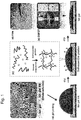
- Fig. 1 the ink preparation and synthesis of an ion gel ink and deposited ion gel is shown, whereby in Fig. 1a ) a gelled ion gel is shown and in Fig. 1b ) an excess of solvent has been introduced to avoid the gelation. To effectively inhibit the gelation an excessive amount of solvent into the solution which evaporates after printed and triggers the self-assembly is added.
- the polymerization has been characterized via different techniques like Fourier transform infrared spectroscopy (FT-IR), X-Ray diffraction analysis (XRD) or scanning electron microscopy (SEM).
- FT-IR Fourier transform infrared spectroscopy
- XRD X-Ray diffraction analysis
- SEM scanning electron microscopy
- the ion-gel ink has been optimized to fabricate a chemically cross-linked ion gel by self-assembled gelation in a straightforward process.
- poly(vinyl alcohol) and poly(ethylene-alt-maleic anhydride) were used as polymer backbone and chemical cross-linker, and 1-ethyl-3-methylimidazolium trifluoromethanesulfonate ([EMIM][OTf]) is utilized as an ionic component to this system to make it functional as an electrolyte.
- the synthesized ion gel exhibits a remarkable ionic conductivity of ⁇ 5 mS cm -1 and an effective capacitance of 5.4 ⁇ F cm -2 at 1 Hz.
- the ion gel has been successfully employed in electrolyte-gated FETs (EGFETs) with indium oxide (In 2 O 3 ) channel, which shows an on/off-ratio of 1.31 ⁇ 10 6 and a subthreshold swing of 80.62 mV s -1 .
- the ion gel ink enables ink-jet printing of chemically crosslinked ion gels and to avoid complex synthesis processes such as annealing, UV-curing, and reversible addition-fragmentation chain transfer (RAFT) polymerization.
- RAFT reversible addition-fragmentation chain transfer
- PVa poly(vinyl acetate)
- the peak at 1473 in PVA/PEMA ion gel results from in-plane asymmetric stretching band of (N) CH 2 , (N)CH 3 , and CN of [EMIM] ( Fig. 2d ). Based on the FT-IR results, we determined that chemical cross-linkage was structured by self-assembled gelation during solvent evaporation.
- the film of PVA/PEMA ion gel is analyzed by impedance spectroscopy in the frequency range from 100 kHz to 1 Hz.
- Fig. 3a shows a log (
- Fig. 3b shows an ionic conductivity ( ⁇ ) versus frequency plot of the PVA/PEMA ion gel.
- ⁇ ionic conductivity
- C eff Effective capacitance (C eff ) of PVA/PEMA ion gel is plotted in Fig. 3c .
- C eff is calculated by Equation 1 and 2. (The details of the calculation are explained in supporting information)
- C eff ⁇ 1 2 ⁇ fZ im
- C eff ⁇ Z im 2 ⁇ f Z 2
- Equation 1 has been generally used to calculate C eff to evaluate the EDLs.
- C eff calculated by Equation 1 (C eff-1 is largely deviated in high-frequency range and only valid in low-frequency range, where the phase angle is close to a pure capacitive response of -90°.
- n-type top-gated EGFETs based on n-type indium oxide (In 2 O 3 ) channel are fabricated.
- indium oxide precursor is ink-jet printed between the lithographically structured drain and source electrodes.
- the gate insulator either PVA/PEMA ion gel or CSPE, is printed on top of the channel.
- PEDOT:PSS is printed on top of those, covering the channel area.
- the drain current (I d ) and gate leakage current (I g ) are plotted versus the gate voltage (V g ), comparing ion gel-gated and CSPE-gated FETs.
- the transfer curves in Fig. 4a shows that PVA/PEMA ion gel has the enhanced gating performance. Both EGFETs exhibit similar on/off currents, but PVA/PEMA ion gel-gated FET shows lower hysteresis. The narrower hysteresis indicates that the formation and deformation of the EDLs are much faster due to high ionic conductivity in a practical operation.
- the subthreshold swing values obtained by the ion gel and CSPE-gated FETs are 80.62 mV s -1 and 100.73 mV s -1 , respectively, where S of ion gel-gated FET is very close to the theoretical limit of 60 mV s -1 .
- the threshold voltage (V th ) of the ion gel and CSPE are calculated to be -0.138 V and -0.177 V, respectively. The difference in the threshold voltage is small, indicating that, in this case, the threshold voltage is rather related to the channel materials than to the gate dielectric.
- PVA/PEMA ion gel has the noticeable ionic conductivity and an effective capacitance.
- PVA/PEMA ion gel exhibits the enhanced gate-insulating properties compared to CSPE, and also shows humidity-insensitive performance even at low relative humidity ( ⁇ 20 %).
Landscapes
- Engineering & Computer Science (AREA)
- Manufacturing & Machinery (AREA)
- Chemical & Material Sciences (AREA)
- Materials Engineering (AREA)
- Thin Film Transistor (AREA)
Abstract
Description
- The present invention relates to specific electrolytes for printed electronics especially for electrolyte-gating of field-effect transistors (FETs), their method of preparation and uses.
- Printed electronics has been highlighted to be a very promising technique for the preparation and assembly of low-end power electronics suitable for sensors and devices used in the Internet of Things (IoT). Especially, electrolyte-gated field effect transistors (EGFETs) have been in the focus of interest because of the possibility to use low voltages for operation, and there has been a remarkable progress in the development of semiconducting channels and electrolyte-based gate insulators.
- The EGFETs are switched on/off by applying a gate potential, which induces an electric field between the electrodes. This electric field enables conducting ions to migrate to the semiconductor/electrolyte interface and to form the electric double layer (EDL), generating high charge accumulation in the adjacent semiconducting channel. For this reason, it is important for electrolyte-based gate insulators to derive strong EDL and high ionic conductivity to improve the EGFET performance like switching speed and on/off current. As a remarkable study, Dasgupta et al. [1] suggested the utilization of composite solid polymer electrolytes (CSPE) consisting of poly(vinyl alcohol), propylene carbonate, and lithium perchlorate, and this CSPE exhibited high ionic conductivity (11 mS cm-1) and cut-off frequency (>10 MHz) in the EGFETs. However, an insufficient switching speed of the EGFETs has been still considered as a technical hurdle for the practical use, and various types of advanced polymer electrolytes have been intensively studied and applied for printed transistors.
- A different approach has been established by Choi et al. [2] where an ion gel, consisting of an ionic liquid and a polymer, is used in EGFETs. This approach leads to the use of the intrinsic properties of the ionic liquid such as high ionic conductivity (>1 mS cm-1), high capacitance (∼10 µF cm-2), negligible volatility, and electrochemical stability (>3 V). In general, ion gels are classified into chemically cross-linked (CC) or physically cross-linked (PC) ion gels, depending on the cross-linkage. Among PC ion gels, ABA triblock ion gels which have been considered as cutting-edge ion gels for printed transistors were developed. PC based triblock ion gels exhibit a good tailorable morphology due to the possibility to vary block polymers and chain length. They are fabricated by reversible gelation on the EGFETs, where a hydrophobic A block is entangled to form a physical cross-linkage. On the other hand, CC ion gels have been less studied compared to PC ion gels due to a much higher difficulty to control the morphology and to fabricate the EGFETs. For these reasons, studies of CC ion gels have almost only focused on material development such as finding new synthesis methods[3-5] or improving the physical properties and ionic conductivities [6,7], and there have been few reports for a practical use in printed transistors, so far. Moreover, in terms of the fabrications, rigid gel structures of CC ion gels by irreversible gelation is always considered as a technical hurdle to directly use to the ink-jet printing process. Furthermore EGFETs have up to now a high sensibility to humidity.
- The main object of the present invention is therefore to provide an electrolyte, a method for preparing it and its use, which overcome the limitations known from the state of the art.
- In particular, it is an object of the present invention to provide an electrolyte for printing electronics, which is printable, stable and insensitive to humidity.
- Is it a further object if the present invention to provide a method for preparing a printable electrolyte, which is fast and easy to perform and in particular avoiding an additional synthesis process step of stabilization or subsequent treatment as for example via annealing at high temperatures, UV-curing or radical polymerization.
- The solution of this problem is provided by an electrolyte for printing electronics according to
claim 1, a method for preparing it according to claim 6, a printed device comprising said electrolyte according to claim 11 and the use of said electrolyte according to claim 15.
The dependent claims describe preferred features. - The term "chemical crosslinking" or "chemical crosslinked" is the process of linking polymer chains by covalent bondings, forming tridimensional networks which reduce the mobility of the structure and usually enhance its mechanical and barrier properties and its water resistance.
- The term "film" is the ion gel ink after deposition on a substrate and evaporation of the solvent, which is used for impedance measurements or physical characterization.
- According to the present invention an electrolyte for printing electronics is provided comprising:
- at least one backbone polymer
- at least one chemical cross-linker
- at least one solvent
- at least one ionic liquid.
- In a preferred embodiment, the at least one backbone polymer has at least one hydroxyl group and the at least one chemical cross-linker is a polymer comprising at least one maleic anhydride group. This hydroxyl/anhydride reaction leads to a covalent binding and is the basis of the chemical cross-linked structure of the polymer. The simple mixing of a polymer comprising at least one maleic anhydride group and a polymer comprising at least one hydroxyl group lead to a gelation occurring by self-assembly. This is also the reason, why a copolymer obtained by this reaction has not been used yet for printing applications for example as printing electrolyte, as the gelation occurs before the step of printing. For the printing step, this gel could be used as it is not viscous enough.
- In a preferred embodiment the amount of the at least one solvent is equal to or at higher than 90% preferably ≥ 95%, particularly preferred ≥ 98%, the sum of the amount of the at least one backbone polymer and the amount of the at least one chemical crosslinker. As the solvent is added in excessive amounts towards the backbone polymer and the chemical crosslinker in the electrolyte, the gelation does not occur immediately. The composition of the present invention can thus be used as a printed electrolyte i.e. for printing electronics. In the state of the art, chemical crosslinked polymer mixtures were not printable, as either the polymerization occurs before the printing process, whereby the viscosity of the mixture would be so high, that the printing is not possible. Or the cross-linking is achieved after the step of printing and needs therefore a further step of initiation.
- In a preferred embodiment the at least one chemical cross-linker is poly(ethylene-alt-maleic anhydride) (PEMA) or poly(methyl vinyl ether-alt-maleic anhydride (PVME-MA) and particularly preferred poly(ethylene-alt-maleic anhydride) (PEMA).
- In a preferred embodiment the at least one backbone polymer is poly(vinyl alcohol) (PVA). The polymer combination of PEMA and PVA or PVME-MA and PVA leads to a copolymer in form of a gel.
- The gelation occurs by self-assembly, so that the simple mixing of the PEMA and PVA or PVME-MA leads to a non-printable mixture.
- In a preferred embodiment, the at least one solvent is Dimethylsulfoxide DMSO. Further the amount of DMSO is equal or higher than 95% and preferred equal or higher than 98% as the sum of the amounts of PVA and PEMA. Indeed under 95%, the gelation does not occur at room temperature, between 95% and 98%, the gelation occurs at room temperature but slowly, so that printing is possible, when performed fast enough and over 98% the gelation is inhibited till the printing and the subsequent evaporation of DMSO, which is the optimal case.
- Preferably the ratio of the amount of the at least one chemical cross-linker to the amount of the at least one backbone polymer is lower than 50:50 preferably between 40:60 and 20:80, more preferred between 25:75 and 35:65, in particular 30:70. If the ratio of the amount of the at least one chemical cross-linker to the amount of the at least one backbone polymer is higher than 50:50, the gelation does not occur.
- In a preferred embodiment the at least one ionic liquid comprises 1-Ethyl-3-methylimidazolium [EMIM] as cation, preferably the ionic liquid is preferably 1-Ethyl-3-methylimidazoliumtrifluoromethanesulfonate [EMIM][OTf] or 1-Ethyl-3-bis(trifluoromethanesulfonyl)imide [EMIM][TFSI], particularly preferred [EMIM][OTf]. [OTf] is preferred as it has a hydrophilic property and works in 20%-90% of relative humidity in air. [TFSI] is more difficult to use in the depositing step, as it has a hydrophobic property. Indeed, the liquid ion gel ink comprising [TFSI] will either be repelled by the substrate, so that the precise positioning of the ion gel ink on the substrate is difficult.
- The ionic liquid comprises the conducting ion in the ion gel mixture or composite. The higher the amount of ionic liquid, the greater the conductivity till a saturation limit. The addition of ionic liquid in the ion gel slows the gelation process, because the interaction between the ionic liquid and the functional groups like the hydroxyl group and the anhydride group hinders the reaction of the functional groups among themselves.
- This invention provides further a method for preparing an electrolyte for printed electronics comprising the following steps:
- a) providing a mixture comprising at least one backbone polymer, at least one chemical cross-linker, at least one solvent, whereas the amount of the at least one solvent is higher or equal than 90%, preferably ≥ 95% and more preferred ≥ 98% of the sum of the amount of the at least one backbone polymer and the amount of the at least one chemical crosslinker,
- b) adding at least one ionic liquid to get an ion gel ink (2),
- c) depositing the obtained ion gel ink (2) on a substrate (3), whereby the deposited ion gel is obtained.
- Preferably after step c) a drying time is implemented which preferably amounts to less than 10 minutes, particularly preferred less than 5 minutes. 5 minutes are sufficient for the ion gel ink to get into the solid phase and for the field-effect transistor comprising the present electrolyte to get a good performance.
- The deposited ion gel is preferably in a solidified state, when the ion gel ink droplets have fully disappeared. From this moment on, the substrate with the deposited ion gel can be used for its final application preferably to printing the top gate when used as electrolyte.
- In an alternative embodiment the backbone polymer and/or the chemical cross-linker are filtered. This step of filtration occurs preferably before the addition of the ionic liquid to minimize the loss of ionic liquid. The step of filtration remove the long polymer chain, i.e. the polymer chain with a high molar mass distribution Mw, and it influences the physical properties like strength. The ion gel ink could not be printable in an ink-jet printer with a nozzle size, which is not compatible with the molar mass distribution of the polymers used. Another possibility is to use a dilute solution of the ion gel ink.
- In a preferred embodiment the ion gel ink is dried after step c) at room temperature or at a temperature between 15°C and 50°C, more preferably between 25°C and 45°C and particularly preferred between 30°C-40°C. The minimum temperature is 15 °C preferably 25°C and particularly preferred 30°C. The maximum temperature is 50°C preferably 45°C and particularly preferred 40°C. A minimum temperature is needed for the gelation to occur and for the cross-linking to have already progressed enough to get a stable ion gel ink. However it is not needed to exceed 50°C to obtain a chemical crosslinked ion gel ink with the properties of chemical stability, ion conductivity and printability and for the use as electrolyte in printing devices. In case of a temperature above room temperature a heating device is used to dry the ion gel ink once deposited.
- In a preferred embodiment the step c) is obtained by printing the obtained ion gel ink on a substrate preferably by ink-jet printing or spin coating, particularly preferred by ink-jet printing.
- The advantage of the present method according to the invention is to avoid any step, which is necessary to initiate the polymerization. A subsequent annealing step particularly at a temperature > 50°C, and more particularly above room temperature is not needed. Furthermore no UV-curing or reversible addition fragmentation chain transfer polymerization or any conventional initiation step for polymerization is needed.
- This invention thus provides a method for preparing an electrolyte for printed electronics consisting of the following steps:
- a) providing a mixture comprising at least one backbone polymer, at least one chemical cross-linker, at least one solvent, whereas the amount of the at least one solvent is higher or equal than 90%, preferably ≥ 95% and more preferred ≥ 98%) of the sum of the amount of the at least one backbone polymer and the amount of the at least one chemical crosslinker,
- b) adding at least one ionic liquid to get an ion gel ink (2),
- c) depositing the obtained ion gel ink (2) on a substrate (3), whereby a deposited ion gel (4) is obtained.
- The deposited ion gel (4) is in the chemical state of the ion gel after self-assembly has occurred and after evaporation of the solvent.
- It is a further aspect of this invention to provide a field-effect transistor comprising at least one electrolyte according to the invention.
- In a preferred embodiment it is an electrolyte-gated field effect transistor (EGFET), i.e. the gating is achieved by the electrolyte.
- Moreover the field-effect transistor preferably comprises a semiconducting channel, a gate insulator comprising at least the printed electrolyte according to the invention, at least a first electrode and at least a second electrode.
- In a preferred embodiment the semiconducting channel are indium oxide nanoparticles (In2O3), the at least first electrode is PEDOT:PSS and the at least second electrode is a patterned-ITO electrode.
- This invention provides furthermore the use of the electrolyte according to the invention for printing electronics.
- The advantage of the present invention is to provide a printable chemical crosslinked polymer mixture without the need of a subsequent treatment for the initiation of the polymerization. In the state of the art an initiation of the cross-linking is needed for example via annealing at high temperatures above 200°C. Thus with the present invention applications with heat- or UV-sensitive substrates or flexible substrate like polymers can be used, as they would decompose at high temperatures above 200°C.
- A further advantage of the present invention towards the state of the art is that the electrolyte is insensitive to humidity especially humidity present in air and can be used in a wide application range. In the state of the art the electrolyte are sensitive to humidity, which would modify the properties of the electrolyte, when used in a transistor. The function of the transistor would be limited or partially non-working. Here humidity-insensitive performance even at low relative humidity (∼20 %) is shown.
- Another effect reached by a field-effect transistor especially by an electrolyte gated field effect transistor comprising the electrolyte of the present invention are the enhanced gate-insulating properties as well as a remarkable ionic conductivity and an effective capacitance.
- The invention will be explained in more detail in the following working examples and figures, which each represent preferred embodiments of the invention, whereby:
-
Fig. 1 shows a schematic representation of the method of the present invention with the ink preparation and synthesis of (a) an ion gel (with ion liquid) (b)ink-jet printable ion-gel ink (dilute solution) c) self-assembled gelation of ion-gel ink during solvent evaporation d) ion-gel film and e) top-gated, ion-gel-gated thin-film transistor. -
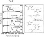
Fig. 2 Shows FT-IR absorbance spectrums of: (a) PEMA film, (b) PVA film, (c) PVA/PEMA polymeric gel film, (d) PVA/PEMA ion gel film. DMSO is fully evaporated in order to clearly observe the polymer structure. (e) Polymer structure of PVA, PEMA, and PVA/PEMA polymeric gel. -
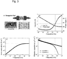
Fig. 3 shows an (a) illustration of a Swagelok cell assembled with two electrodes and an ion-gel film. (b) Bode plot, (c) ionic conductivity versus frequency plot, and (d) effective capacitance (Ceff) versus frequency plot of PVA/PEMA ion-gel film. Ionic conductivity and capacitance were calculated based on impedance results. Temperature is room temperature (25 °C). Film thickness and diameter are 1.1 mm and 12 mm, respectively. -
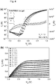
Fig. 4 shows the output characterization of top-gated EGFETs; (a) gate-source voltage (Vg) versus drain-source current (Id) and gate leakage current (Ig) plots of PVA/PEMA ion gel and CSPE at 40 % of relative humidity (RH) and 1 V of drain-source voltage (Vd), (b) Vd versus Id plot of PVA/PEMA ion gel at 40 % RH. Channel length and width are 200 µm and 60 µm. -
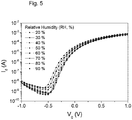
Fig. 5 . shows Gate-source voltage (Vg) versus drain-source current (Id) plot of PVA/PEMA ion gel-gated FETs at 1 Vd at different relative humidity (RH, %) from 20 % to 90 %. - In
Fig. 1 the ink preparation and synthesis of an ion gel ink and deposited ion gel is shown, whereby inFig. 1a ) a gelled ion gel is shown and inFig. 1b ) an excess of solvent has been introduced to avoid the gelation. To effectively inhibit the gelation an excessive amount of solvent into the solution which evaporates after printed and triggers the self-assembly is added. - The polymerization has been characterized via different techniques like Fourier transform infrared spectroscopy (FT-IR), X-Ray diffraction analysis (XRD) or scanning electron microscopy (SEM). The printability has been investigated as well as the use as electrolyte for FET.
- The ion-gel ink has been optimized to fabricate a chemically cross-linked ion gel by self-assembled gelation in a straightforward process. For self-assembled gelation, poly(vinyl alcohol) and poly(ethylene-alt-maleic anhydride) were used as polymer backbone and chemical cross-linker, and 1-ethyl-3-methylimidazolium trifluoromethanesulfonate ([EMIM][OTf]) is utilized as an ionic component to this system to make it functional as an electrolyte. A polymeric gel of PVA and PEMA in DMSO (polymer : solvent = 4 : 96 wt%) without [EMIM] [OTf], and an ion gel ink consisting of PVA,PEMA, [EMIM][OTf], and DMSO (PVA : PEMA : [EMIM][OTf] : DMSO = 0.6 : 0.3 : 2 : 97.1 wt%) have been synthetized.
- The synthesized ion gel exhibits a remarkable ionic conductivity of ∼5 mS cm-1 and an effective capacitance of 5.4 µF cm-2 at 1 Hz. The ion gel has been successfully employed in electrolyte-gated FETs (EGFETs) with indium oxide (In2O3) channel, which shows an on/off-ratio of 1.31×10⁶ and a subthreshold swing of 80.62 mV s-1.
- The ion gel ink enables ink-jet printing of chemically crosslinked ion gels and to avoid complex synthesis processes such as annealing, UV-curing, and reversible addition-fragmentation chain transfer (RAFT) polymerization. To ensure ink-jet printability, it is crucial to properly inhibit or promote self-assembled gelation of PVA and PEMA, because the functional groups of PVA and PEMA easily react even at room temperature in concentrated solution, forming a rigid chemical cross-linked gel, which cannot be applied for ink-jet printing.
- In dilute solution, the solvent is bound to the macromolecular coils, and these solvent-swollen coils are separated each other by the excess of solvent. For this reason, the solvent-swollen coils loss their mutual interactions, and suppress the chemical cross-linkage in the diluted solution. For gelation inhibition, the amount of solvent is significant.
The gelation of PVA and PEMA was simply conducted by solvent evaporation. During the evaporation, the solvent trapped by macromolecular coils of PVA and PEMA is released, and PVA and PEMA are able to mutually interact and to form the cross-linkage. This self-assembled gelation does not require an additional initiation step, because the ring-opening reaction between the functional groups of PVA and PEMA is spontaneous and can easily proceed in the solution. By this method, we could fabricate a CC PVA/PEMA ion gel on the substrate by ink-jet printing. - The self-assembly of the CC structure could be tracked by FT-IR spectroscopy. In
Fig. 2a the cyclic anhydride of PEMA shows two intrinsic peaks at 1844 and 1782 cm-1, corresponding to C=O symmetric and asymmetric stretching bands, respectively. With these peaks, we could determine that the hydroxyl (-OH) groups of PVA react with the cyclic anhydride of PEMA by nucleophilic attack. When solvent-swollen coils of PVA and PEMA become reactive by releasing the absorbed solvent during solvent evaporation, the cyclic anhydride is spontaneously opened by structuring to carboxylic acid and ester (Fig. 2e ). During this ring-opening reaction, a broad peak overlapping the C=O carbonyl bands of carboxylic acid at 1717 cm-1 and ester at 1720 cm-1 appears, whereas symmetric and asymmetric C=O stretching bands of cyclic anhydride at 1844 and 1782 cm-1 were slightly observed in the spectra of PVA/PEMA gel (Fig. 2c ) and PVA/PEMA ion gel (Fig. 2d ). The peak at 1700-1720 cm-1 in PEMA spectra is attributed to C=O band of maleic acid which maleic anhydride is hydrolyzed by nucleophilic attack of water molecules, and the small peak at ∼1720 cm-1 in PVA spectra is C=O band of poly(vinyl acetate) (PVa), which is the residue in commercial PVA powder (Fig. S1). The peak at 1473 in PVA/PEMA ion gel results from in-plane asymmetric stretching band of (N) CH2, (N)CH3, and CN of [EMIM] (Fig. 2d ). Based on the FT-IR results, we determined that chemical cross-linkage was structured by self-assembled gelation during solvent evaporation. - The film of PVA/PEMA ion gel is analyzed by impedance spectroscopy in the frequency range from 100 kHz to 1 Hz.
Fig. 3a shows a log (|Z|) versus frequency plot, which depicts a plateau indicating the bulk resistance (Rbulk) in the range above 30 kHz. Above this frequency, conducting ions in a polymeric gel are not able to be accumulated to the inner and outer Helmholtz planes (IHP and OHP) due to insufficient time for ion migration, and the EDLs cannot be formed. As the frequency was decreased, the value of log (|Z|) was increased and became a tilted straight line below 3.7 kHz, corresponding to a phase angle of -45°, where the polarization behavior of the EDLs is changed from resistive to capacitive. Below 400 Hz, the phase angle was saturated between -70° and 75°. The deviations between a saturated phase angle of -63° and an ideal capacitive response of -90° results from non-ideal capacitive behavior. - In addition,
Fig. 3b shows an ionic conductivity (σ) versus frequency plot of the PVA/PEMA ion gel. At high frequencies above 30 kHz, a plateau region of Rbulk is observed, and the ionic conductivity is calculated to be ∼5 mS cm-1. As frequency is lowered, ionic conductivity started to decrease because of the electrode polarization by the EDLs at the electrolyte/electrode interface. The plot of ionic conductivity was linearly declined below 3.7 kHz as PVA/PEMA ion gel exhibited the capacitive behavior. - Effective capacitance (Ceff) of PVA/PEMA ion gel is plotted in
Fig. 3c . Ceff is calculated byEquation 

Equation 1 has been generally used to calculate Ceff to evaluate the EDLs. However, some groups suggested that Ceff calculated by Equation 1 (Ceff-1 is largely deviated in high-frequency range and only valid in low-frequency range, where the phase angle is close to a pure capacitive response of -90°. InFig. 3c , it could be observed large deviation between Ceff-1 and Ceff-2 in high frequency range (> 3.7 kHz), where the EDLs cannot be formed and the only resistive response is dominant in impedance spectroscopy. Ceff-2 exhibited the drastically declined plot in the resistive range, whereas Ceff-1 has a linear shape. Considering that the EDLs cannot be formed in high-frequency ranges, we conservatively determined that Ceff-2 is more reliable, and measured to be 5.4 µF cm-2 at 1 Hz. - To investigate the characteristics of PVA/PEMA ion gel as the gate insulator, n-type top-gated EGFETs based on n-type indium oxide (In2O3) channel are fabricated. For that purpose, indium oxide precursor is ink-jet printed between the lithographically structured drain and source electrodes. After an annealing step at 400 °C, the gate insulator, either PVA/PEMA ion gel or CSPE, is printed on top of the channel. After the gelation of PVA/PEMA ion gel or the dry of CSPE, PEDOT:PSS is printed on top of those, covering the channel area. In
Fig. 4a , the drain current (Id) and gate leakage current (Ig) are plotted versus the gate voltage (Vg), comparing ion gel-gated and CSPE-gated FETs. The transfer curves inFig. 4a shows that PVA/PEMA ion gel has the enhanced gating performance. Both EGFETs exhibit similar on/off currents, but PVA/PEMA ion gel-gated FET shows lower hysteresis. The narrower hysteresis indicates that the formation and deformation of the EDLs are much faster due to high ionic conductivity in a practical operation. The parameter of subthreshold swing (S) shows how much change in gate-voltage is needed to increase the drain-source current by one decade and is calculated as follows:
- The subthreshold swing values obtained by the ion gel and CSPE-gated FETs are 80.62 mV s-1 and 100.73 mV s-1, respectively, where S of ion gel-gated FET is very close to the theoretical limit of 60 mV s-1. In addition, the threshold voltage (Vth) of the ion gel and CSPE are calculated to be -0.138 V and -0.177 V, respectively. The difference in the threshold voltage is small, indicating that, in this case, the threshold voltage is rather related to the channel materials than to the gate dielectric.
- In addition, we tested the influence of humidity on PVA/PEMA ion gel-gated FETs. In the previous study, Marques et al. identified that CSPE easily losses the ionic conductivity in lower relative humidity (RH) ranges (≤ 20 %) . As reason is found that trapped solvent of DMSO is evaporated in low humidity condition and the ion-transferring channel in the polymer matrix is disconnected. Fig. S7 shows Id and Id 1/2 versus Vg plots of CSPE-gated FET measured at 20 % RH. Compared to the transfer curve measured at 40 % RH (
Fig. 4a ), Ion is drastically decreased from 6.08×10⁻⁴ A to 3.73×10⁻⁴ A, and the hysteresis becomes much wider, resulted from slow the formation or deformation of EDLs, due to the low ionic conductivity. However, PVA/PEMA ion gel-gated FETs show stable transfer curves even at low RH of 20 % because of the negligible volatility of [EMIM][OTf] in the polymeric gel (Fig. 5 ). In addition, the Vth and the S parameters are stable in the range from 30 % to 60 % RH, whereas both parameters are increasing with humidity in CSPE-gated FETs. Even though in high RH levels (≥ 70 %) the Vth and the S were slightly changed in PVA/PEMA ion gel-gated FETs. Nevertheless, this result clearly shows stable performance over all of RH levels.Table 1. Electrical parameters of PVA/PEMA ion gel-gated field effect transistors at different relative humidity (RH) Relative Humidity [%] Off current [A] On current [A] On/off current ratio [104] Subthres hold swing [mV s-1] Threshold voltage [V] 20 4.01×10⁻¹⁰ 6.86×10⁻⁴ 13.7 82.71 -0.241 30 4.46×10⁻¹⁰ 6.97×10⁻⁴ 14.3 80.71 -0.149 40 4.01×10⁻¹⁰ 6.14×10⁻⁴ 12.3 78.49 -0.161 40 4.37×10⁻¹⁰ 7.04×10⁻⁴ 13.1 80.62 -0.138 60 6.44×10⁻¹⁰ 4.89×10⁻⁴ 8.99 80.73 -0.144 70 1.44×10⁻⁹ 7.67×10⁻⁴ 4.31 84.94 -0.186 80 2.07×10⁻⁹ 7.76×10⁻⁴ 3.74 84.30 -0.217 90 2.30×10⁻⁹ 8.21×10⁻⁴ 3.48 86.01 -0.24 - Moreover, it is been shown that PVA/PEMA ion gel has the noticeable ionic conductivity and an effective capacitance. In n-type top-gated EGFETs, PVA/PEMA ion gel exhibits the enhanced gate-insulating properties compared to CSPE, and also shows humidity-insensitive performance even at low relative humidity (∼20 %).
-
- [1] S. Dasgupta, G. Stoesser, N. Schweikert, R. Hahn, S. Dehm, R. Kruk, H. Hahn, Advanced Functional Materials 2012, 22, 4909.
- [12] J.-H. Choi, W. Xie, Y. Gu, C. D. Frisbie, T. P. Lodge, ACS Applied Materials & Interfaces 2014, 7, 7294.
- [3] Y. Gu, S. Zhang, L. Martinetti, K. H. Lee, L. D. McIntosh, . D. Frisbie, T. P. Lodge, Journal of the American Chemical Society 2013, 134, 9642.
- [4] M. A. B. H. Susan, T. Kaneko, A. Noda, M. Watanabe, Journal of the American Chemical Society 2004, 127, 4976.
- [5] G. Martinez-Ponce, C. Solano, Optics Express 2006, 14, 3776.
- [6] M. A. Klingshirn, S. K. Spear, R. Subramanian, J. D. Holbrey, J. G. Huddleston, R. D. Rogers, Chemistry of Materials 2004, 16, 3091.
- [7] K. Matsumoto, T. Endo, Macromolecules 2008, 41, 6981.
Claims (15)
- Electrolyte for printing electronics comprising at least one backbone polymer, at least one chemical cross-linker, at least one solvent and at least one ionic liquid, whereas the backbone polymer has at least one hydroxyl group and the at least one chemical cross-linker is a polymer comprising at least one maleic anhydride group and whereas the amount of the at least one solvent is higher or equal than 90% of the sum of the amount of the at least one backbone polymer and the amount of the at least one chemical crosslinker.
- Electrolyte for printing electronics according to claim 1, whereas the at least one chemical cross-linker is poly(ethylene-alt-maleic anhydride) (PEMA) or poly(methyl vinyl ether-alt-maleic anhydride (PVME-MA) and particularly preferred poly(ethylene-alt-maleic anhydride) (PEMA).
- Electrolyte for printing electronics according to claim 1 or 2, whereas the ratio of the amount of the at least one chemical cross-linker to the amount of the at least one backbone polymer is lower than 1 preferably between 20:80 and 40:60, more preferred between 25:75 and 35:65, in particular 30:70.
- Electrolyte for printing electronics according to one of the claims 1 to 3, whereas the at least one backbone polymer is poly(vinyl alcohol) (PVA).
- Electrolyte for printing electronics according to one of claims 1 to 4, whereas the at least one ionic liquid comprises 1-Ethyl-3-methylimidazolium [EMIM] as cation and is preferably 1-Ethyl-3-methylimidazoliumtrifluoromethanesulfonate [EMIM][OTf] or 1-Ethyl-3-bis(trifluoromethanesulfonyl)imide [EMIM][TFSI], particularly preferred [EMIM][OTf].
- Method for preparing an electrolyte for printed electronics comprising the following steps:a) providing a mixture comprising at least one backbone polymer, at least one chemical cross-linker, at least one solvent, whereas the amount of the at least one solvent is higher or equal than 90% of the sum of the amount of the at least one backbone polymer and the amount of the at least one chemical crosslinker,b) adding at least one ionic liquid to get an ion gel ink,c) depositing the obtained ion gel ink on a substrate, whereby a deposited ion gel is obtained.
- Method for preparing an electrolyte for printed electronics according to claim 6, comprising the step:
d) waiting for the evaporation of the solvent, which preferably lasts less than 10 minutes, particularly preferred less than 5 minutes. - Method for preparing an electrolyte for printing electronics according to claim 6 or 7, whereas the backbone polymer and/or the chemical cross-linker are filtered.
- Method for preparing an electrolyte for printing electronics according to one of the claims 6 to 8, whereas after step c) the ion gel ink is dried at a temperature between 15°C and 50°C, preferably between 25°C and 45°C and particularly preferred between 30°C-40°C.
- Method for preparing an electrolyte for printing electronics according to one of the claims 6 to 9, whereas the step c) is obtained by printing the obtained ion gel ink on a substrate preferably by ink-jet printing.
- Field-effect transistor comprising at least one electrolyte prepared by the method according to one of the claims 6 to 10.
- Field-effect transistor according to claim 11, whereas the gating is achieved by the electrolyte.
- Field-effect transistor according to claim 11 or 12, comprising a semiconducting channel, a gate insulator comprising at least the electrolyte, at least a first electrode and at least a second electrode.
- Field-effect transistor according to one of the claims 11 to 13, whereas the semiconducting channel are indium oxide nanoparticles (In2O3), the at least first electrode is PEDOT:PSS and the at least second electrode is a patterned-ITO electrode.
- Use of the electrolyte according to one of the claims 1 to 5 for printing electronics.
Priority Applications (1)
| Application Number | Priority Date | Filing Date | Title |
|---|---|---|---|
| EP19401021.1A EP3745465A1 (en) | 2019-05-28 | 2019-05-28 | Electrolyte for printable electronics, method for its preparation and use |
Applications Claiming Priority (1)
| Application Number | Priority Date | Filing Date | Title |
|---|---|---|---|
| EP19401021.1A EP3745465A1 (en) | 2019-05-28 | 2019-05-28 | Electrolyte for printable electronics, method for its preparation and use |
Publications (1)
| Publication Number | Publication Date |
|---|---|
| EP3745465A1 true EP3745465A1 (en) | 2020-12-02 |
Family
ID=66821168
Family Applications (1)
| Application Number | Title | Priority Date | Filing Date |
|---|---|---|---|
| EP19401021.1A Pending EP3745465A1 (en) | 2019-05-28 | 2019-05-28 | Electrolyte for printable electronics, method for its preparation and use |
Country Status (1)
| Country | Link |
|---|---|
| EP (1) | EP3745465A1 (en) |
Citations (1)
| Publication number | Priority date | Publication date | Assignee | Title |
|---|---|---|---|---|
| EP2629356A1 (en) * | 2012-02-17 | 2013-08-21 | Karlsruher Institut für Technologie | Composite solid polymer electrolyte, its use, and printed electronics manufactured by means of said composite solid polymer electrolyte |
-
2019
- 2019-05-28 EP EP19401021.1A patent/EP3745465A1/en active Pending
Patent Citations (1)
| Publication number | Priority date | Publication date | Assignee | Title |
|---|---|---|---|---|
| EP2629356A1 (en) * | 2012-02-17 | 2013-08-21 | Karlsruher Institut für Technologie | Composite solid polymer electrolyte, its use, and printed electronics manufactured by means of said composite solid polymer electrolyte |
Non-Patent Citations (10)
| Title |
|---|
| CADILHA MARQUES GABRIEL ET AL: "Influence of Humidity on the Performance of Composite Polymer Electrolyte-Gated Field-Effect Transistors and Circuits", IEEE TRANSACTIONS ON ELECTRON DEVICES, IEEE SERVICE CENTER, PISACATAWAY, NJ, US, vol. 66, no. 5, 1 May 2019 (2019-05-01), pages 2202 - 2207, XP011720515, ISSN: 0018-9383, [retrieved on 20190419], DOI: 10.1109/TED.2019.2903456 * |
| CHARU ROHATGI ET AL: "Separator Membrane from Crosslinked Poly(Vinyl Alcohol) and Poly(Methyl Vinyl Ether-alt-Maleic Anhydride)", NANOMATERIALS, vol. 5, no. 2, 25 March 2015 (2015-03-25), pages 398 - 414, XP055607202, DOI: 10.3390/nano5020398 * |
| G. MARTINEZ-PONCEC. SOLANO, OPTICS EXPRESS, vol. 14, 2006, pages 3776 |
| J.-H. CHOIW. XIEY. GUC. D. FRISBIET. P. LODGE, ACS APPLIED MATERIALS & INTERFACES, vol. 7, 2014, pages 7294 |
| JEONG HO CHO ET AL: "Printable ion-gel gate dielectrics for low-voltage polymer thin-film transistors on plastic", NATURE MATERIALS, NATURE PUBLISHING GROUP, LONDON, GB, vol. 7, 1 November 2008 (2008-11-01), pages 900 - 906, XP007910676, ISSN: 1476-4660, [retrieved on 20081019], DOI: 10.1038/NMAT2291 * |
| K. MATSUMOTOT. ENDO, MACROMOLECULES, vol. 41, 2008, pages 6981 |
| M. A. B. H. SUSANT. KANEKOA. NODAM. WATANABE, JOURNAL OF THE AMERICAN CHEMICAL SOCIETY, vol. 127, 2004, pages 4976 |
| M. A. KLINGSHIRNS. K. SPEARR. SUBRAMANIANJ. D. HOLBREYJ. G. HUDDLESTONR. D. ROGERS, CHEMISTRY OF MATERIALS, vol. 16, 2004, pages 3091 |
| S. DASGUPTAG. STOESSERN. SCHWEIKERTR. HAHNS. DEHMR. KRUKH. HAHN, ADVANCED FUNCTIONAL MATERIALS, vol. 22, 2012, pages 4909 |
| Y. GUS. ZHANGL. MARTINETTIK. H. LEEL. D. MCINTOSHD. FRISBIET. P. LODGE, JOURNAL OF THE AMERICAN CHEMICAL SOCIETY, vol. 134, 2013, pages 9642 |
Similar Documents
| Publication | Publication Date | Title |
|---|---|---|
| Huang et al. | Dielectric materials for electrolyte gated transistor applications | |
| Tang et al. | Synergistic increase in ionic conductivity and modulus of triblock copolymer ion gels | |
| Choi et al. | Single ion conducting, polymerized ionic liquid triblock copolymer films: high capacitance electrolyte gates for n-type transistors | |
| Duraikkan et al. | Structural, thermal and electrical properties of polyvinyl alcohol/poly (vinyl pyrrolidone)–sodium nitrate solid polymer blend electrolyte | |
| US7646013B2 (en) | Transistor with large ion-complexes in electrolyte layer | |
| DE69332598T2 (en) | Ion-conducting polymer electrolyte | |
| Rozik et al. | A novel approach on poly (ionic liquid)-based poly (vinyl alcohol) as a hydrophilic/hydrophobic conductive polymer electrolytes | |
| Seol et al. | Highly conductive, binary ionic liquid–solvent mixture ion gels for effective switching of electrolyte-gated transistors | |
| Li et al. | Humidity sensors based on the composite of multi-walled carbon nanotubes and crosslinked polyelectrolyte with good sensitivity and capability of detecting low humidity | |
| EP2606076A1 (en) | Process for producing breakdown-resistant ultrathin dielectrics in electronic components using crosslinkable polymeric dielectric materials | |
| Thiemann et al. | Spray-coatable ionogels based on silane-ionic liquids for low voltage, flexible, electrolyte-gated organic transistors | |
| Cyriac et al. | Modification in the microstructure of sodium carboxymethylcellulose/polyvinyl alcohol polyblend films through the incorporation of NaNO3 for energy storage applications | |
| Cho et al. | Thermostable ion gels for high-temperature operation of electrolyte-gated transistors | |
| Ramesh et al. | Conductivity, dielectric behaviour and thermal stability studies of lithium ion dissociation in poly (methyl methacrylate)-based gel polymer electrolytes | |
| Lee et al. | Highly conductive and mechanically robust nanocomposite polymer electrolytes for solid-state electrochemical thin-film devices | |
| Tousignant et al. | Poly (ionic liquid) dielectric for high performing P-and N-type single walled carbon nanotube transistors | |
| EP2812931B1 (en) | Electronic devices comprising photocurable polymeric materials | |
| Suthanthiraraj et al. | Effect of propylene carbonate as a plasticizer on (PEO) 50AgCF3SO3: SnO2 nanocomposite polymer electrolyte | |
| WO2016118536A2 (en) | Printable high dielectric constant and self-healable dielectric polymer composition | |
| KR20190050595A (en) | Physically crosslinked ion gel and preparation method of the same | |
| Kaihovirta et al. | Printed all-polymer electrochemical transistors on patterned ion conducting membranes | |
| KR101006893B1 (en) | Flexible organic thin film transistor and its manufacturing method | |
| Suthanthiraraj et al. | Electrical and structural properties of poly (ethylene oxide)/silver triflate polymer electrolyte system dispersed with MgO nanofillers | |
| Sinno et al. | Amphiphilic semiconducting copolymer as compatibility layer for printing polyelectrolyte-gated OFETs | |
| Regu et al. | Al2O3-incorporated proton-conducting solid polymer electrolytes for electrochemical devices: a proficient method to achieve high electrochemical performance |
Legal Events
| Date | Code | Title | Description |
|---|---|---|---|
| PUAI | Public reference made under article 153(3) epc to a published international application that has entered the european phase |
Free format text: ORIGINAL CODE: 0009012 |
|
| STAA | Information on the status of an ep patent application or granted ep patent |
Free format text: STATUS: THE APPLICATION HAS BEEN PUBLISHED |
|
| AK | Designated contracting states |
Kind code of ref document: A1 Designated state(s): AL AT BE BG CH CY CZ DE DK EE ES FI FR GB GR HR HU IE IS IT LI LT LU LV MC MK MT NL NO PL PT RO RS SE SI SK SM TR |
|
| AX | Request for extension of the european patent |
Extension state: BA ME |
|
| STAA | Information on the status of an ep patent application or granted ep patent |
Free format text: STATUS: REQUEST FOR EXAMINATION WAS MADE |
|
| 17P | Request for examination filed |
Effective date: 20210527 |
|
| RBV | Designated contracting states (corrected) |
Designated state(s): AL AT BE BG CH CY CZ DE DK EE ES FI FR GB GR HR HU IE IS IT LI LT LU LV MC MK MT NL NO PL PT RO RS SE SI SK SM TR |
|
| STAA | Information on the status of an ep patent application or granted ep patent |
Free format text: STATUS: EXAMINATION IS IN PROGRESS |
|
| 17Q | First examination report despatched |
Effective date: 20240614 |
|
| 17Q | First examination report despatched |
Effective date: 20240625 |
|
| REG | Reference to a national code |
Ref country code: DE Ref legal event code: R079 Free format text: PREVIOUS MAIN CLASS: H01L0029423000 Ipc: H10K0071130000 |
|
| RIC1 | Information provided on ipc code assigned before grant |
Ipc: H10K 71/13 20230101AFI20260302BHEP Ipc: H01G 11/56 20130101ALI20260302BHEP Ipc: H01G 9/035 20060101ALI20260302BHEP Ipc: H01M 10/0565 20100101ALI20260302BHEP Ipc: H01G 9/028 20060101ALI20260302BHEP Ipc: H10K 71/15 20230101ALI20260302BHEP Ipc: H10K 85/10 20230101ALI20260302BHEP |
|
| GRAP | Despatch of communication of intention to grant a patent |
Free format text: ORIGINAL CODE: EPIDOSNIGR1 |
|
| STAA | Information on the status of an ep patent application or granted ep patent |
Free format text: STATUS: GRANT OF PATENT IS INTENDED |
|
| INTG | Intention to grant announced |
Effective date: 20260409 |