EP3745176A1 - Connector - Google Patents
Connector Download PDFInfo
- Publication number
- EP3745176A1 EP3745176A1 EP20177409.8A EP20177409A EP3745176A1 EP 3745176 A1 EP3745176 A1 EP 3745176A1 EP 20177409 A EP20177409 A EP 20177409A EP 3745176 A1 EP3745176 A1 EP 3745176A1
- Authority
- EP
- European Patent Office
- Prior art keywords
- circuit board
- housing
- shield case
- shield
- shield cover
- Prior art date
- Legal status (The legal status is an assumption and is not a legal conclusion. Google has not performed a legal analysis and makes no representation as to the accuracy of the status listed.)
- Granted
Links
Images


Classifications
-
- H—ELECTRICITY
- H01—ELECTRIC ELEMENTS
- H01R—ELECTRICALLY-CONDUCTIVE CONNECTIONS; STRUCTURAL ASSOCIATIONS OF A PLURALITY OF MUTUALLY-INSULATED ELECTRICAL CONNECTING ELEMENTS; COUPLING DEVICES; CURRENT COLLECTORS
- H01R13/00—Details of coupling devices of the kinds covered by groups H01R12/70 or H01R24/00 - H01R33/00
- H01R13/648—Protective earth or shield arrangements on coupling devices, e.g. anti-static shielding
-
- G—PHYSICS
- G02—OPTICS
- G02B—OPTICAL ELEMENTS, SYSTEMS OR APPARATUS
- G02B6/00—Light guides; Structural details of arrangements comprising light guides and other optical elements, e.g. couplings
- G02B6/24—Coupling light guides
- G02B6/42—Coupling light guides with opto-electronic elements
- G02B6/4201—Packages, e.g. shape, construction, internal or external details
- G02B6/4274—Electrical aspects
- G02B6/4277—Protection against electromagnetic interference [EMI], e.g. shielding means
-
- G—PHYSICS
- G02—OPTICS
- G02B—OPTICAL ELEMENTS, SYSTEMS OR APPARATUS
- G02B6/00—Light guides; Structural details of arrangements comprising light guides and other optical elements, e.g. couplings
- G02B6/24—Coupling light guides
- G02B6/42—Coupling light guides with opto-electronic elements
- G02B6/4201—Packages, e.g. shape, construction, internal or external details
- G02B6/4274—Electrical aspects
- G02B6/428—Electrical aspects containing printed circuit boards [PCB]
-
- H—ELECTRICITY
- H01—ELECTRIC ELEMENTS
- H01R—ELECTRICALLY-CONDUCTIVE CONNECTIONS; STRUCTURAL ASSOCIATIONS OF A PLURALITY OF MUTUALLY-INSULATED ELECTRICAL CONNECTING ELEMENTS; COUPLING DEVICES; CURRENT COLLECTORS
- H01R13/00—Details of coupling devices of the kinds covered by groups H01R12/70 or H01R24/00 - H01R33/00
- H01R13/648—Protective earth or shield arrangements on coupling devices, e.g. anti-static shielding
- H01R13/658—High frequency shielding arrangements, e.g. against EMI [Electro-Magnetic Interference] or EMP [Electro-Magnetic Pulse]
- H01R13/6581—Shield structure
-
- G—PHYSICS
- G02—OPTICS
- G02B—OPTICAL ELEMENTS, SYSTEMS OR APPARATUS
- G02B6/00—Light guides; Structural details of arrangements comprising light guides and other optical elements, e.g. couplings
- G02B6/24—Coupling light guides
- G02B6/42—Coupling light guides with opto-electronic elements
- G02B6/4201—Packages, e.g. shape, construction, internal or external details
- G02B6/4256—Details of housings
- G02B6/426—Details of housings mounting, engaging or coupling of the package to a board, a frame or a panel
- G02B6/4261—Packages with mounting structures to be pluggable or detachable, e.g. having latches or rails
-
- G—PHYSICS
- G02—OPTICS
- G02B—OPTICAL ELEMENTS, SYSTEMS OR APPARATUS
- G02B6/00—Light guides; Structural details of arrangements comprising light guides and other optical elements, e.g. couplings
- G02B6/24—Coupling light guides
- G02B6/42—Coupling light guides with opto-electronic elements
- G02B6/4292—Coupling light guides with opto-electronic elements the light guide being disconnectable from the opto-electronic element, e.g. mutually self aligning arrangements
-
- H—ELECTRICITY
- H01—ELECTRIC ELEMENTS
- H01R—ELECTRICALLY-CONDUCTIVE CONNECTIONS; STRUCTURAL ASSOCIATIONS OF A PLURALITY OF MUTUALLY-INSULATED ELECTRICAL CONNECTING ELEMENTS; COUPLING DEVICES; CURRENT COLLECTORS
- H01R13/00—Details of coupling devices of the kinds covered by groups H01R12/70 or H01R24/00 - H01R33/00
- H01R13/648—Protective earth or shield arrangements on coupling devices, e.g. anti-static shielding
- H01R13/658—High frequency shielding arrangements, e.g. against EMI [Electro-Magnetic Interference] or EMP [Electro-Magnetic Pulse]
- H01R13/6591—Specific features or arrangements of connection of shield to conductive members
- H01R13/6594—Specific features or arrangements of connection of shield to conductive members the shield being mounted on a PCB and connected to conductive members
Definitions
- the present invention relates to a connector.
- a periphery of a connector housing is covered with a shield case made of a conductive metal plate (see, for example, Patent Literatures 1 to 3).
- a plate spring portion for holding an internal electronic component may be formed on the shield case by cutting and raising. For this reason, a slit for cutting and raising is formed around the plate spring portion on the shield case, and thereby a shielding performance may be deteriorated.
- a terminal contact prevention gap must be provided between the circuit board and the shield case, and the shielding performance may be further deteriorated.
- the present invention has been made in view of the above circumstances, and an object thereof is to provide a connector having a high shielding performance.
- the optical connector including the photoelectric conversion module can be a high-performance optical connector in which the shielding performance is high and the deviation of an optical axis is suppressed.
- the connector that ensures the high shielding performance can be provided.
- an optical connector as a connector used in the optical communication field will be described as an example.
- FIG. 1 is a perspective view of an optical connector 10 according to an embodiment of the present invention.
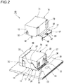
- FIG. 2 is a perspective view of the optical connector 10 shown in FIG. 1 with a shield cover 70 removed.
- the optical connector (connector) 10 is a receptacle optical connector to which a mating side optical connector as a plug connector is joined.
- the optical connector 10 is mounted on a circuit board 11, and the mating side optical connector (not shown) is fitted and connected thereto.
- a shield cover 70 is mounted on an outer peripheral side of the optical connector 10.
- the circuit board 11 includes through holes 12 for solder connection, through holes 13 for compliant pins, and a contact pad 14 for grounding.
- the through holes 12, 13 and the contact pad 14 for grounding are all connected to the ground of the circuit board 11.
- FIG. 3 is an exploded perspective view of the optical connector 10.
- the optical connector 10 includes a housing 20, a shield case 30, a lens body 40, a photoelectric conversion module (hereinafter, also referred to as fiber optic transceiver (FOT)) 50 as an electronic component, and a shield cover 70.
- FOT fiber optic transceiver
- the housing 20 is a box-shaped member formed of a synthetic resin.
- the housing 20 is formed with a fitting recessed portion 21 into which the mating optical connector is fitted on a front end side.
- the housing 20 is provided with a ferrule (not shown) therein, and an end portion of an optical fiber (not shown) of the mating side optical connector fitted in the fitting recessed portion 21 is fitted into the ferrule.
- the lens body 40 and the FOT 50 are assembled to the housing 20 from a rear end side.
- the shield case 30 is fitted into and mounted on the housing 20 from an upper portion.
- the housing 20 includes locking plate portions 23 each lock a side plate portion 32, which will be described later, of the shield case 30 on both side surfaces 22 thereof.
- the locking plate portion 23 is connected to the side surface 22 of the housing 20 by a connecting portion 24 extending in an upper-lower direction.
- the shield case 30 is formed into a box shape and includes a top plate portion 31, the side plate portions 32 formed on both sides of the top plate portion 31, and a rear plate portion 33 formed on a rear side of the top plate portion 31.
- the shield case 30 is bent and formed into the box shape by pressing a conductive metal plate or the like.
- the shield case 30 is mounted on the housing 20 to cover and shield the upper portion, both of the side portions, and a rear portion of the housing 20.
- a plurality of leg portions 34 are formed on the side plate portion 32. The leg portions 34 are inserted into the through holes 12 for solder connection of the circuit board 11 and soldered. Accordingly, the optical connector 10 is fixed to the circuit board 11, and the shield case 30 is connected to the ground of the circuit board 11.
- the shield case 30 includes locking slits 35 each extending upward from a lower edge of the side plate portion 32.
- the side plate portion 32 of the shield case 30 is fitted into a gap between the side surface 22 of the housing 20 and the locking plate portion 23.
- the connecting portion 24 connecting the locking plate portion 23 to the housing 20 is inserted into the locking slit 35 of the side plate portion 32.
- the rear plate portion 33 includes a pair of plate spring portions 36 protruding inward (see FIG. 2 ). These plate spring portions 36 are formed on the rear plate portion 33 of the shield case 30 by cutting and raising after the periphery of portions serving as the plate spring portions 36 is cut to form slits for cutting and raising.
- the plate spring portion 36 presses and urges a rear surface of the FOT 50 housed in the housing 20. Accordingly, the lens body 40 and the FOT 50 housed in the housing 20 are held in a state in which rattling with respect to the housing 20 is suppressed by an elastic urging force of the plate spring portion 36.
- the lens body 40 and the FOT 50 are assembled from the rear end side of the housing 20.
- the lens body 40 and the FOT 50 are combined with each other so as to be positioned.
- the lens body 40 and the FOT 50 are assembled to the housing 20 in a state of being combined with each other.
- the lens body 40 includes a substrate portion 43 formed in a rectangular shape in a plan view, and a light emitting side lens portion 41 and a light receiving side lens portion 42 are formed on the substrate portion 43.
- the light emitting side lens portion 41 and the light receiving side lens portion 42 are provided side by side.
- the lens body 40 is integrally formed of a transparent resin having light guiding properties, so that the light emitting side lens portion 41 and the light receiving side lens portion 42 are integrally provided to protrude forward from a front surface of the substrate portion 43.
- the FOT 50 is formed in a rectangular shape in the plan view, and a light emitting side FOT 51 and a light receiving side FOT 52 are provided side by side on a front surface of the FOT 50.
- the light emitting side FOT 51 includes, for example, a light emitting element such as a light emitting diode (LED), a vertical cavity surface emitting laser (VCSEL), and the light receiving side FOT 52 includes, for example, a light receiving element such as a photo diode (PD).
- the FOT 50 is integrally formed of a synthetic resin, so that the light emitting side FOT 51 and the light receiving side FOT 52 are integrally provided.
- a plurality of leads (terminals) 55 are provided at a lower portion of the FOT 50.
- a tip end portion of the lead 55 is bent toward a rear side of the FOT 50, and the lead 55 is disposed and soldered on a pad (not shown) formed on a surface of the circuit board 11, and electrically connected to a predetermined circuit of the circuit board 11 (see FIG. 2 ).
- the optical connector 10 is mounted on the circuit board 11 by the surface mount technology (SMT).
- the lens body 40 and the FOT 50 are fitted from behind the housing 20 and housed in a positioned state. Accordingly, the light emitting side lens portion 41 and the light receiving side lens portion 42 of the lens body 40 are inserted into lens insertion holes (not shown) formed on the housing 20, and are positioned in the ferrule in the housing 20.
- an optical signal converted and generated from an electrical signal by the light emitting side FOT 51 of the FOT 50 is incident on the light emitting side lens portion 41 of the lens body 40, and is guided to the optical fiber of the mating side optical connector joined to the fitting recessed portion 21. Further, an optical signal incident on the light receiving side lens portion 42 from another optical fiber of the mating side optical connector is emitted from the light receiving side lens portion 42 of the lens body 40, received by the light receiving side FOT 52 of the FOT 50, and converted into an electrical signal.
- the optical connector 10 includes the shield case 30, leakage of noise from the FOT 50 as an internal electronic component and intrusion of noise from an external electronic component or the like are suppressed.
- the plate spring portion 36 is provided on the rear plate portion 33 of the shield case 30, so that a slit for cutting and raising 37 is formed around the plate spring portion 36.
- a terminal contact prevention gap 38 is formed between the surface of the circuit board 11 and a lower edge of the rear plate portion 33 of the shield case 30 in order to avoid contact with the leads 55 for surface mounting.
- a locking slit 35 for being locked to the housing 20 is formed on each of the two side plate portions 32 of the shield case 30.
- the shielding performance can be enhanced by mounting the shield cover 70.
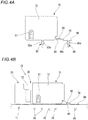
- FIGS. 4A and 4B are views illustrating the shield cover 70 shown in FIG. 3 , in which FIG. 4A is a side view of the shield cover 70, and FIG. 4B is a side view of the optical connector 10.
- the shield cover 70 includes a top plate 71, side plates 72 formed on both sides of the top plate 71, and a rear plate 73 formed on a rear side of the top plate 71.
- the shield cover 70 is formed in a box shape that can be mounted over a rear portion of the shield case 30. Further, the shield cover 70 includes an extension portion 74 extending rearward from a lower edge of the rear plate 73. Similar to the shield case 30, the shield cover 70 is formed into a box shape by pressing a conductive metal plate or the like.
- a contact piece 81 protruding inward is formed on each side plate 72 of the shield cover 70.
- the contact piece 81 comes into contact with the two side plate portions 32 of the shield case 30 by mounting the shield cover 70 over the shield case 30. Accordingly, the shield cover 70 is conducted with the shield case 30.
- a compliant pin 82 having a pair of outwardly bulging contacts 82a is provided on a lower edge of the side plate 72 of the shield cover 70 so as to protrude downward.
- the extension portion 74 includes an upper plate portion 85 and a lower plate portion 86 in order from a rear plate 73 side.
- the lower plate portion 86 is disposed lower than the upper plate portion 85.
- a plate-shaped insulating member 90 made of an insulating material such as an insulating synthetic resin is provided on the lower surface side of the upper plate portion 85.
- Contact pieces 87 protruding downward are formed in a center portion in a width direction of the lower plate portion 86.
- the compliant pin 88 having the pair of outwardly bulging contacts 88a is provided on each of both ends of the lower plate portion 86 so as to protrude downward.
- the shield cover 70 is put on the housing 20 and the shield case 30 which are mounted on the circuit board 11 from above. Then, the compliant pins 82, 88 of the two side plates 72 and the extension portion 74 are inserted into the through holes 13 for compliant pins of the circuit board 11.
- the shield cover 70 is fixed to the circuit board 11 in a state in which the contacts 82a, 88a of the respective compliant pins 82, 88 are in contact with plated parts on inner surfaces of the through holes 13 and conduct well. Further, the contact pieces 87 provided on the extension portion 74 of the shield cover 70 come into contact with the contact pad 14 for grounding of the circuit board 11 and conduct well. Accordingly, the shield cover 70 is brought into conduction with the ground of the circuit board 11. The contact pieces 81 of the two side plates 72 of the shield cover 70 come into contact with outer surfaces of the two side plate portions 32 of the shield case 30. Accordingly, the shield cover 70 is well conducted with the shield case 30. Since the extension portion 74 is provided with the insulating member 90 on the lower surface of the upper plate portion 85, the lead 55 of the FOT 50 is ensured in the insulating state with respect to the shield cover 70.
- the shield cover 70 when the shield cover 70 is mounted on the housing 20 to which the shield case 30 is mounted, the slit for cutting and raising 37 around the plate spring portion 36 of the rear plate portion 33 of the shield case 30 is covered with the rear plate 73 of the shield cover 70. Further, the terminal contact prevention gap 38 between the surface of the circuit board 11 and the lower edge of the rear plate portion 33 of the shield case 30 is covered by the extension portion 74 of the shield cover 70. Further, the locking slits 35 formed on the two side plate portions 32 are covered by the two side plates 72 of the shield cover 70, respectively.
- the gaps of the shield case 30, such as the slit for cutting and raising 37 around the plate spring portion 36 holding the internal FOT 50, and the locking slit 35 for locking the shield case 30 to the housing 20, are covered by the shield cover 70 fixed to the circuit board 11. Accordingly, the noise emitted from the FOT 50 and the noise emitted from peripheral electronic components and the like can be reliably absorbed by the shield case 30 and the shield cover 70.
- the shield cover 70 that covers an outer surface of the shield case 30 is fixed to the circuit board 11. Therefore, when the high shielding performance is required, the shielding performance can be enhanced by mounting the shield cover 70 as necessary without improving the housing 20 or the shield case 30 itself.
- the shield cover 70 includes the compliant pins 82, 88 inserted into the through holes 13 formed on the circuit board 11. Therefore, by inserting the compliant pins 82, 88 into the through holes 13, the shield cover 70 can be easily fixed to the circuit board 11. Accordingly, it is possible to save time and labor for fixing the shield cover 70 to the circuit board 11 by soldering and the like. Further, by inserting the compliant pins 82, 88 into the through holes 13 connected to the ground of the circuit board 11, the shield cover 70 can be easily conducted to the ground. Accordingly, it is possible to save time and labor for electrically connecting the shield cover 70 to the circuit board 11 by soldering and the like.
- the extension portion 74 of the shield cover 70 can suppress leakage or intrusion of noise in the terminal contact prevention gap 38 between the lower edge of the rear plate portion 33 of the shield case 30 and the surface of the circuit board 11, and the shielding performance can be further enhanced.
- the contact pieces 87 of the extension portion 74 are in elastic contact with the contact pad 14 for grounding of the circuit board 11. Therefore, the shield cover 70 can be easily connected to the ground through the contact pad 14 for grounding of the circuit board 11.
- the optical connector 10 since the FOT 50 is pressed and urged against the housing 20 by the plate spring portion 36 of the shield case 30, rattling of the FOT 50 housed in the housing 20 can be suppressed and a vibration resistance can be enhanced. That is, the optical connector 10 including the FOT 50 can be a high-performance optical connector in which the shielding performance is high and the deviation of an optical axis is suppressed.
- the optical connector 10 having a structure for suppressing leakage and intrusion of noise by the shield case 30 has been described as an example, but the present invention can be applied to various connectors for suppressing leakage and intrusion of noise by covering the housing on which the electronic component are mounted with the shield case.
- the present invention is not limited to an optical connector, and can also be applied to an electrical connector for high-speed transmission.
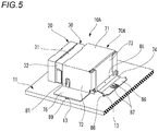
- FIG. 5 is a perspective view of an optical connector 10A according to a modification of the present invention.
- extension portions 75 are formed on both side portions of a shield cover 70A. These extension portions 75 extend laterally from the lower edges of the side plates 72 of the shield cover 70A.
- Compliant pins 89 each having a pair of outwardly bulging contacts (not shown) are provided on end portions of these extension portions 75 respectively so as to protrude downward. These compliant pins 89 are fixed to the circuit board 11 while being inserted into the through-holes 13 for compliant pins of the circuit board 11 and conducted to the ground.
- the slit for cutting and raising 37 around the plate spring portion 36, the terminal contact prevention gap 38 between the surface of the circuit board 11 and the lower edge of the rear plate portion 33 of the shield case 30, and the locking slit 35 can be covered (see FIG. 2 ).
- the gap 39 (see FIG. 2 ) between the circuit board 11 and the lower edge of the side plate portion 32 of the shield case 30 can be further covered by the extension portion 75. Accordingly, in the optical connector 10A, leakage and intrusion of noise can be further suppressed by the shield cover 70A, and the high shielding performance can be obtained.
Landscapes
- Physics & Mathematics (AREA)
- General Physics & Mathematics (AREA)
- Optics & Photonics (AREA)
- Electromagnetism (AREA)
- Optical Couplings Of Light Guides (AREA)
- Details Of Connecting Devices For Male And Female Coupling (AREA)
- Coupling Device And Connection With Printed Circuit (AREA)
Abstract
Description
- The present invention relates to a connector.
- For example, in order to improve a noise performance, for an optical connector used in an optical communication field or an I/O connector having a high data transfer rate, a periphery of a connector housing is covered with a shield case made of a conductive metal plate (see, for example, Patent Literatures 1 to 3).
-
- Patent Literature 1:
JP-A-2009-69710 - Patent Literature 2:
JP-A-2014-119691 - Patent Literature 3:
JP-A-2013-508937 - On the above connector, a plate spring portion for holding an internal electronic component may be formed on the shield case by cutting and raising. For this reason, a slit for cutting and raising is formed around the plate spring portion on the shield case, and thereby a shielding performance may be deteriorated.
- Further, in the connector mounted on a circuit board by the surface mount technology (SMT), in order to avoid a terminal of the electronic component connected to a pad on a surface of the circuit board, a terminal contact prevention gap must be provided between the circuit board and the shield case, and the shielding performance may be further deteriorated.
- The present invention has been made in view of the above circumstances, and an object thereof is to provide a connector having a high shielding performance.
- The above object of the present invention is achieved by the following configurations.
- (1) A connector includes: a housing provided on a circuit board; an electronic component housed in the housing and having a terminal which is configured to be electrically connected to the circuit board; a shield case covering the housing and fixed to the circuit board; and a shield cover covering at least a gap of the shield case and fixed to the circuit board.
According to the connector having the configuration of (1), gaps of the shield case, such as a slit for cutting and raising around the plate spring portion holding the internal electronic component, and the locking slit for locking the shield case to the housing, are covered by the shield cover fixed to the circuit board. Accordingly, the noise emitted from the electronic component and the noise emitted from a peripheral electronic component and the like can be reliably absorbed by the shield case and the shield cover.
Further, the shield cover is fixed to the circuit board. Therefore, when the high shielding performance is required, the shielding performance can be enhanced by covering the gaps of the shield case as necessary without improving the housing or the shield case itself. - (2) In the connector according to (1), the shield cover includes a compliant pin inserted into a through hole which is formed on the circuit board.
According to the connector having the configuration of (2), by inserting the compliant pin into the through hole connected to the ground of the circuit board, the shield cover can be easily fixed to the circuit board, and the shield cover can be easily conducted to the ground. Accordingly, it is possible to save time and labor for electrically connecting and fixing the shield cover to the circuit board by soldering and the like. - (3) In the connector according to (1) or (2), the shield cover includes an extension portion extending along a surface of the circuit board and covering a gap between a lower edge of the shield case and the circuit board.
According to the connector having the configuration of (3), the extension portion of the shield cover can suppress leakage or intrusion of noise in the gap between the lower edge of the shield case and the circuit board and the terminal contact prevention gap, and the shielding performance can be further enhanced. - (4) In the connector according to (3), the extension portion includes a contact piece which is in elastic contact with a contact pad for grounding provided on the circuit board.
According to the connector having the configuration of (4), the contact piece of the extension portion is in elastic contact with the contact pad for grounding of the circuit board. Therefore, the shield cover can be easily connected to the ground through the contact pad for grounding of the circuit board. - (5) In the connector according to any one of (1) to (4), a photoelectric conversion module as the electronic component is housed in the housing, and a plate spring portion configured to press and urge the photoelectric conversion module and held the photoelectric conversion module in the housing is formed on the shield case, and the shield cover is mounted so as to cover at least a region of the shield case where the plate spring portion is formed.
- (6) In the connector according to (5), a lens body including a lens unit is housed in the housing, and the photoelectric conversion module is attached to the lens body.
- According to the connector having the configuration of (5), since the photoelectric conversion module is pressed and urged against the housing by the plate spring portion of the shield case, rattling of the photoelectric conversion module housed in the housing can be suppressed and a vibration resistance can be enhanced. That is, the optical connector including the photoelectric conversion module can be a high-performance optical connector in which the shielding performance is high and the deviation of an optical axis is suppressed.
- According to the present invention, the connector that ensures the high shielding performance can be provided.
- The present invention has been briefly described above. Further, details of the present invention will be clarified by reading a mode (hereinafter, referred to as "embodiment") for carrying out the invention to be described below with reference to the accompanying drawings.
-
-
FIG. 1 is a perspective view of an optical connector according to an embodiment of the present invention. -
FIG. 2 is a perspective view of the optical connector shown inFIG. 1 with a shield cover removed. -
FIG. 3 is an exploded perspective view of the optical connector shown inFIG. 1 . -
FIGS. 4A and 4B are views illustrating the shield cover shown inFIG. 3 , in whichFIG. 4A is a side view of the shield cover, andFIG. 4B is a side view of the optical connector. -
FIG. 5 is a perspective view of an optical connector according to a modification of the present invention. - Hereinafter, an embodiment according to the present invention will be described with reference to the drawings.
- In the present embodiment, an optical connector as a connector used in the optical communication field will be described as an example.
-
FIG. 1 is a perspective view of anoptical connector 10 according to an embodiment of the present invention.FIG. 2 is a perspective view of theoptical connector 10 shown inFIG. 1 with ashield cover 70 removed. - As shown in
FIGS. 1 and2 , the optical connector (connector) 10 according to the present embodiment is a receptacle optical connector to which a mating side optical connector as a plug connector is joined. Theoptical connector 10 is mounted on acircuit board 11, and the mating side optical connector (not shown) is fitted and connected thereto. Ashield cover 70 is mounted on an outer peripheral side of theoptical connector 10. - The
circuit board 11 includes throughholes 12 for solder connection, throughholes 13 for compliant pins, and acontact pad 14 for grounding. The throughholes contact pad 14 for grounding are all connected to the ground of thecircuit board 11. -
FIG. 3 is an exploded perspective view of theoptical connector 10. - As shown in
FIG. 3 , theoptical connector 10 includes ahousing 20, ashield case 30, alens body 40, a photoelectric conversion module (hereinafter, also referred to as fiber optic transceiver (FOT)) 50 as an electronic component, and ashield cover 70. - The
housing 20 is a box-shaped member formed of a synthetic resin. Thehousing 20 is formed with a fitting recessedportion 21 into which the mating optical connector is fitted on a front end side. Thehousing 20 is provided with a ferrule (not shown) therein, and an end portion of an optical fiber (not shown) of the mating side optical connector fitted in the fitting recessedportion 21 is fitted into the ferrule. Thelens body 40 and theFOT 50 are assembled to thehousing 20 from a rear end side. Theshield case 30 is fitted into and mounted on thehousing 20 from an upper portion. Further, thehousing 20 includeslocking plate portions 23 each lock aside plate portion 32, which will be described later, of theshield case 30 on bothside surfaces 22 thereof. Thelocking plate portion 23 is connected to theside surface 22 of thehousing 20 by a connectingportion 24 extending in an upper-lower direction. - The
shield case 30 is formed into a box shape and includes atop plate portion 31, theside plate portions 32 formed on both sides of thetop plate portion 31, and arear plate portion 33 formed on a rear side of thetop plate portion 31. Theshield case 30 is bent and formed into the box shape by pressing a conductive metal plate or the like. - The
shield case 30 is mounted on thehousing 20 to cover and shield the upper portion, both of the side portions, and a rear portion of thehousing 20. A plurality ofleg portions 34 are formed on theside plate portion 32. Theleg portions 34 are inserted into the throughholes 12 for solder connection of thecircuit board 11 and soldered. Accordingly, theoptical connector 10 is fixed to thecircuit board 11, and theshield case 30 is connected to the ground of thecircuit board 11. - Further, the
shield case 30 includes locking slits 35 each extending upward from a lower edge of theside plate portion 32. Theside plate portion 32 of theshield case 30 is fitted into a gap between theside surface 22 of thehousing 20 and thelocking plate portion 23. At this time, the connectingportion 24 connecting the lockingplate portion 23 to thehousing 20 is inserted into the locking slit 35 of theside plate portion 32. - Further, the
rear plate portion 33 includes a pair ofplate spring portions 36 protruding inward (seeFIG. 2 ). Theseplate spring portions 36 are formed on therear plate portion 33 of theshield case 30 by cutting and raising after the periphery of portions serving as theplate spring portions 36 is cut to form slits for cutting and raising. Theplate spring portion 36 presses and urges a rear surface of theFOT 50 housed in thehousing 20. Accordingly, thelens body 40 and theFOT 50 housed in thehousing 20 are held in a state in which rattling with respect to thehousing 20 is suppressed by an elastic urging force of theplate spring portion 36. - The
lens body 40 and theFOT 50 are assembled from the rear end side of thehousing 20. Thelens body 40 and theFOT 50 are combined with each other so as to be positioned. Thelens body 40 and theFOT 50 are assembled to thehousing 20 in a state of being combined with each other. - The
lens body 40 includes asubstrate portion 43 formed in a rectangular shape in a plan view, and a light emittingside lens portion 41 and a light receivingside lens portion 42 are formed on thesubstrate portion 43. The light emittingside lens portion 41 and the light receivingside lens portion 42 are provided side by side. Thelens body 40 is integrally formed of a transparent resin having light guiding properties, so that the light emittingside lens portion 41 and the light receivingside lens portion 42 are integrally provided to protrude forward from a front surface of thesubstrate portion 43. - The
FOT 50 is formed in a rectangular shape in the plan view, and a light emittingside FOT 51 and a light receivingside FOT 52 are provided side by side on a front surface of theFOT 50. The light emittingside FOT 51 includes, for example, a light emitting element such as a light emitting diode (LED), a vertical cavity surface emitting laser (VCSEL), and the light receivingside FOT 52 includes, for example, a light receiving element such as a photo diode (PD). TheFOT 50 is integrally formed of a synthetic resin, so that the light emittingside FOT 51 and the light receivingside FOT 52 are integrally provided. A plurality of leads (terminals) 55 are provided at a lower portion of theFOT 50. A tip end portion of thelead 55 is bent toward a rear side of theFOT 50, and thelead 55 is disposed and soldered on a pad (not shown) formed on a surface of thecircuit board 11, and electrically connected to a predetermined circuit of the circuit board 11 (seeFIG. 2 ). Thus, theoptical connector 10 is mounted on thecircuit board 11 by the surface mount technology (SMT). - The
lens body 40 and theFOT 50 are fitted from behind thehousing 20 and housed in a positioned state. Accordingly, the light emittingside lens portion 41 and the light receivingside lens portion 42 of thelens body 40 are inserted into lens insertion holes (not shown) formed on thehousing 20, and are positioned in the ferrule in thehousing 20. - In the
optical connector 10, an optical signal converted and generated from an electrical signal by the light emittingside FOT 51 of theFOT 50 is incident on the light emittingside lens portion 41 of thelens body 40, and is guided to the optical fiber of the mating side optical connector joined to the fitting recessedportion 21. Further, an optical signal incident on the light receivingside lens portion 42 from another optical fiber of the mating side optical connector is emitted from the light receivingside lens portion 42 of thelens body 40, received by the light receivingside FOT 52 of theFOT 50, and converted into an electrical signal. - Since the
optical connector 10 includes theshield case 30, leakage of noise from theFOT 50 as an internal electronic component and intrusion of noise from an external electronic component or the like are suppressed. - On the other hand, as shown in
FIG. 2 , theplate spring portion 36 is provided on therear plate portion 33 of theshield case 30, so that a slit for cutting and raising 37 is formed around theplate spring portion 36. In a rear portion of theoptical connector 10, a terminalcontact prevention gap 38 is formed between the surface of thecircuit board 11 and a lower edge of therear plate portion 33 of theshield case 30 in order to avoid contact with theleads 55 for surface mounting. Further, as shown inFIG. 3 , a locking slit 35 for being locked to thehousing 20 is formed on each of the twoside plate portions 32 of theshield case 30. - Therefore, when a high shielding performance is required, it is necessary to suppress leakage and intrusion of noise in gaps of the
shield case 30 such as the locking slits 35, the slits for cutting and raising 37, the terminalcontact prevention gap 38. In such a case, in theoptical connector 10 according to the present embodiment, the shielding performance can be enhanced by mounting theshield cover 70. -
FIGS. 4A and 4B are views illustrating theshield cover 70 shown inFIG. 3 , in whichFIG. 4A is a side view of theshield cover 70, andFIG. 4B is a side view of theoptical connector 10. - As shown in
FIGS. 2 to 4 , theshield cover 70 includes atop plate 71,side plates 72 formed on both sides of thetop plate 71, and arear plate 73 formed on a rear side of thetop plate 71. Theshield cover 70 is formed in a box shape that can be mounted over a rear portion of theshield case 30. Further, theshield cover 70 includes anextension portion 74 extending rearward from a lower edge of therear plate 73. Similar to theshield case 30, theshield cover 70 is formed into a box shape by pressing a conductive metal plate or the like. - A
contact piece 81 protruding inward is formed on eachside plate 72 of theshield cover 70. Thecontact piece 81 comes into contact with the twoside plate portions 32 of theshield case 30 by mounting theshield cover 70 over theshield case 30. Accordingly, theshield cover 70 is conducted with theshield case 30. Further, acompliant pin 82 having a pair of outwardly bulgingcontacts 82a is provided on a lower edge of theside plate 72 of theshield cover 70 so as to protrude downward. - The
extension portion 74 includes anupper plate portion 85 and alower plate portion 86 in order from arear plate 73 side. Thelower plate portion 86 is disposed lower than theupper plate portion 85. On the lower surface side of theupper plate portion 85, for example, a plate-shaped insulatingmember 90 made of an insulating material such as an insulating synthetic resin is provided. Contactpieces 87 protruding downward are formed in a center portion in a width direction of thelower plate portion 86. Further, thecompliant pin 88 having the pair of outwardly bulgingcontacts 88a is provided on each of both ends of thelower plate portion 86 so as to protrude downward. - Next, a case in which the
shield cover 70 is mounted on thehousing 20 to which theshield case 30 is mounted will be described. - The
shield cover 70 is put on thehousing 20 and theshield case 30 which are mounted on thecircuit board 11 from above. Then, thecompliant pins side plates 72 and theextension portion 74 are inserted into the throughholes 13 for compliant pins of thecircuit board 11. - Therefore, the
shield cover 70 is fixed to thecircuit board 11 in a state in which thecontacts compliant pins holes 13 and conduct well. Further, thecontact pieces 87 provided on theextension portion 74 of theshield cover 70 come into contact with thecontact pad 14 for grounding of thecircuit board 11 and conduct well. Accordingly, theshield cover 70 is brought into conduction with the ground of thecircuit board 11. Thecontact pieces 81 of the twoside plates 72 of theshield cover 70 come into contact with outer surfaces of the twoside plate portions 32 of theshield case 30. Accordingly, theshield cover 70 is well conducted with theshield case 30. Since theextension portion 74 is provided with the insulatingmember 90 on the lower surface of theupper plate portion 85, thelead 55 of theFOT 50 is ensured in the insulating state with respect to theshield cover 70. - In this way, when the
shield cover 70 is mounted on thehousing 20 to which theshield case 30 is mounted, the slit for cutting and raising 37 around theplate spring portion 36 of therear plate portion 33 of theshield case 30 is covered with therear plate 73 of theshield cover 70. Further, the terminalcontact prevention gap 38 between the surface of thecircuit board 11 and the lower edge of therear plate portion 33 of theshield case 30 is covered by theextension portion 74 of theshield cover 70. Further, the locking slits 35 formed on the twoside plate portions 32 are covered by the twoside plates 72 of theshield cover 70, respectively. - Accordingly, in the
optical connector 10 of the present embodiment, leakage and intrusion of noise in the slits for cutting and raising 37, the locking slits 35, the terminalcontact prevention gap 38, and the like, which are gaps of theshield case 30, are suppressed by theshield cover 70, and the high shielding performance is obtained. - As described above, according to the
optical connector 10 according to the present embodiment, the gaps of theshield case 30, such as the slit for cutting and raising 37 around theplate spring portion 36 holding theinternal FOT 50, and the locking slit 35 for locking theshield case 30 to thehousing 20, are covered by theshield cover 70 fixed to thecircuit board 11. Accordingly, the noise emitted from theFOT 50 and the noise emitted from peripheral electronic components and the like can be reliably absorbed by theshield case 30 and theshield cover 70. - Further, the
shield cover 70 that covers an outer surface of theshield case 30 is fixed to thecircuit board 11. Therefore, when the high shielding performance is required, the shielding performance can be enhanced by mounting theshield cover 70 as necessary without improving thehousing 20 or theshield case 30 itself. - Further, the
shield cover 70 includes thecompliant pins holes 13 formed on thecircuit board 11. Therefore, by inserting thecompliant pins holes 13, theshield cover 70 can be easily fixed to thecircuit board 11. Accordingly, it is possible to save time and labor for fixing theshield cover 70 to thecircuit board 11 by soldering and the like. Further, by inserting thecompliant pins holes 13 connected to the ground of thecircuit board 11, theshield cover 70 can be easily conducted to the ground. Accordingly, it is possible to save time and labor for electrically connecting theshield cover 70 to thecircuit board 11 by soldering and the like. - Furthermore, the
extension portion 74 of theshield cover 70 can suppress leakage or intrusion of noise in the terminalcontact prevention gap 38 between the lower edge of therear plate portion 33 of theshield case 30 and the surface of thecircuit board 11, and the shielding performance can be further enhanced. - When the shield covers 70 are fixed to the
circuit board 11, thecontact pieces 87 of theextension portion 74 are in elastic contact with thecontact pad 14 for grounding of thecircuit board 11. Therefore, theshield cover 70 can be easily connected to the ground through thecontact pad 14 for grounding of thecircuit board 11. - Thus, according to the
optical connector 10 described above, since theFOT 50 is pressed and urged against thehousing 20 by theplate spring portion 36 of theshield case 30, rattling of theFOT 50 housed in thehousing 20 can be suppressed and a vibration resistance can be enhanced. That is, theoptical connector 10 including theFOT 50 can be a high-performance optical connector in which the shielding performance is high and the deviation of an optical axis is suppressed. - In the above-described embodiment, the
optical connector 10 having a structure for suppressing leakage and intrusion of noise by theshield case 30 has been described as an example, but the present invention can be applied to various connectors for suppressing leakage and intrusion of noise by covering the housing on which the electronic component are mounted with the shield case. The present invention is not limited to an optical connector, and can also be applied to an electrical connector for high-speed transmission. - Next, a modification of the present invention will be described.
-
FIG. 5 is a perspective view of anoptical connector 10A according to a modification of the present invention. - As shown in
FIG. 5 , in theoptical connector 10A according to the modification of the present invention,extension portions 75 are formed on both side portions of ashield cover 70A. Theseextension portions 75 extend laterally from the lower edges of theside plates 72 of theshield cover 70A.Compliant pins 89 each having a pair of outwardly bulging contacts (not shown) are provided on end portions of theseextension portions 75 respectively so as to protrude downward. These compliant pins 89 are fixed to thecircuit board 11 while being inserted into the through-holes 13 for compliant pins of thecircuit board 11 and conducted to the ground. - Also in the case of the
optical connector 10A, by mounting theshield cover 70A on thehousing 20 on which theshield case 30 is mounted, the slit for cutting and raising 37 around theplate spring portion 36, the terminalcontact prevention gap 38 between the surface of thecircuit board 11 and the lower edge of therear plate portion 33 of theshield case 30, and the locking slit 35 can be covered (seeFIG. 2 ). According to theoptical connector 10A, the gap 39 (seeFIG. 2 ) between thecircuit board 11 and the lower edge of theside plate portion 32 of theshield case 30 can be further covered by theextension portion 75. Accordingly, in theoptical connector 10A, leakage and intrusion of noise can be further suppressed by theshield cover 70A, and the high shielding performance can be obtained. - The present invention is not limited to the embodiment described above, and modifications, improvements, and the like can be made as appropriate. In addition, the material, shape, size, number, arrangement position, and the like of each component in the above embodiment are optional and are not limited as long as the present invention can be achieved.
- Further, characteristics of the embodiment of the connector according to the present invention described above will be briefly summarized in the following [1] to [6].
- [1] A connector (
optical connector - a housing (20) provided on a circuit board (11);
- an electronic component (photoelectric conversion module (FOT) 50) housed in the housing (20) and having a terminal (lead 55) configured to be electrically connected to the circuit board (11);
- a shield case (30) covering the housing (20) and fixed to the circuit board (11); and
a shield cover (70, 70A) covering at least a gap (slit for cutting and raising 37, locking slit 35) of the shield case (30) and fixed to the circuit board (11).
- [2] In the connector (
optical connector - [3] In the connector (
optical connector contact prevention gap 38, gap 39) between a lower edge of the shield case (30) and the circuit board (11). - [4] In the connector (
optical connector - [5] In the connector (
optical connector
a photoelectric conversion module (FOT 50) as an electronic component is housed in the housing (20),
a plate spring portion (36) configured to press and urge the photoelectric conversion module (FOT 50) and held the photoelectric conversion module in the housing (20) is formed on the shield case (30), and
the shield cover (70, 70A) is mounted so as to cover at least a region of the shield case (30) where the plate spring portion (36) is formed. - [6] In the connector (
optical connector
a lens body (40) including a lens unit (light emittingside lens portion 41, light receiving side lens portion 42) is housed in the housing, and
the photoelectric conversion module is attached to the lens body.
Claims (6)
- A connector comprising:a housing provided on a circuit board;an electronic component housed in the housing and having a terminal which is configured to be electrically connected to the circuit board;a shield case covering the housing and fixed to the circuit board; anda shield cover covering at least a gap of the shield case and fixed to the circuit board.
- The connector according to claim 1,
wherein the shield cover includes a compliant pin inserted into a through hole which is formed on the circuit board. - The connector according to claim 1 or 2,
wherein the shield cover includes an extension portion extending along a surface of the circuit board and covering a gap between a lower edge of the shield case and the circuit board. - The connector according to claim 3,
wherein the extension portion includes a contact piece which is in elastic contact with a contact pad for grounding provided on the circuit board. - The connector according to any one of claims 1 to 4,wherein a photoelectric conversion module as the electronic component is housed in the housing,wherein a plate spring portion configured to press and urge the photoelectric conversion module and held the photoelectric conversion module in the housing is formed on the shield case, andwherein the shield cover is mounted so as to cover at least a region of the shield case where the plate spring portion is formed.
- The connector according to claim 5,wherein a lens body including a lens unit is housed in the housing, andwherein the photoelectric conversion module is attached to the lens body.
Applications Claiming Priority (1)
| Application Number | Priority Date | Filing Date | Title |
|---|---|---|---|
| JP2019101437A JP7099993B2 (en) | 2019-05-30 | 2019-05-30 | connector |
Publications (2)
| Publication Number | Publication Date |
|---|---|
| EP3745176A1 true EP3745176A1 (en) | 2020-12-02 |
| EP3745176B1 EP3745176B1 (en) | 2023-06-14 |
Family
ID=70968740
Family Applications (1)
| Application Number | Title | Priority Date | Filing Date |
|---|---|---|---|
| EP20177409.8A Active EP3745176B1 (en) | 2019-05-30 | 2020-05-29 | Optical connector |
Country Status (4)
| Country | Link |
|---|---|
| US (1) | US11105991B2 (en) |
| EP (1) | EP3745176B1 (en) |
| JP (1) | JP7099993B2 (en) |
| CN (1) | CN112018568B (en) |
Families Citing this family (3)
| Publication number | Priority date | Publication date | Assignee | Title |
|---|---|---|---|---|
| JP2024015846A (en) * | 2022-07-25 | 2024-02-06 | 日本航空電子工業株式会社 | connector with board |
| JP2025003223A (en) * | 2023-06-23 | 2025-01-09 | イリソ電子工業株式会社 | connector |
| JP2025003224A (en) * | 2023-06-23 | 2025-01-09 | イリソ電子工業株式会社 | connector |
Citations (6)
| Publication number | Priority date | Publication date | Assignee | Title |
|---|---|---|---|---|
| JP2009069710A (en) | 2007-09-18 | 2009-04-02 | Yazaki Corp | Optical module |
| DE102010010359A1 (en) * | 2009-03-06 | 2010-09-09 | Alps Electric Co., Ltd. | Optical connector with shielding |
| JP2013508937A (en) | 2009-10-26 | 2013-03-07 | モレックス インコーポレイテド | Shielded connector |
| JP2014119691A (en) | 2012-12-19 | 2014-06-30 | Yazaki Corp | Dust cap and connector engagement body |
| US20160104971A1 (en) * | 2014-10-10 | 2016-04-14 | Dai-lchi Seiko Co., Ltd. | Electrical connector and electrical connector device |
| US20170214187A1 (en) * | 2016-01-27 | 2017-07-27 | Samsung Electronics Co., Ltd. | Connector |
Family Cites Families (8)
| Publication number | Priority date | Publication date | Assignee | Title |
|---|---|---|---|---|
| JPH04102571U (en) * | 1991-02-08 | 1992-09-03 | 日本電気株式会社 | contact pin |
| CN101015095B (en) * | 2004-07-07 | 2012-05-09 | 莫莱克斯公司 | Keyed housings for use with small profile plug connectors |
| US7422464B2 (en) * | 2004-07-07 | 2008-09-09 | Molex Incorporated | Mechanism for delatching small size plug connectors |
| JP2011048034A (en) * | 2009-08-26 | 2011-03-10 | Yazaki Corp | Shield structure for optical connector |
| JP5690510B2 (en) * | 2010-06-28 | 2015-03-25 | 矢崎総業株式会社 | Electronic components |
| JP2014052506A (en) * | 2012-09-07 | 2014-03-20 | Auto Network Gijutsu Kenkyusho:Kk | Optical connector, communication substrate and communication device |
| JP2014110593A (en) * | 2012-12-04 | 2014-06-12 | Hitachi Cable Ltd | Optical communication module |
| CN204424610U (en) * | 2015-03-20 | 2015-06-24 | 东莞市扬明精密塑胶五金电子有限公司 | USB 3.1 Type-C socket connector |
-
2019
- 2019-05-30 JP JP2019101437A patent/JP7099993B2/en not_active Expired - Fee Related
-
2020
- 2020-05-29 CN CN202010474623.8A patent/CN112018568B/en not_active Expired - Fee Related
- 2020-05-29 US US16/888,630 patent/US11105991B2/en not_active Expired - Fee Related
- 2020-05-29 EP EP20177409.8A patent/EP3745176B1/en active Active
Patent Citations (6)
| Publication number | Priority date | Publication date | Assignee | Title |
|---|---|---|---|---|
| JP2009069710A (en) | 2007-09-18 | 2009-04-02 | Yazaki Corp | Optical module |
| DE102010010359A1 (en) * | 2009-03-06 | 2010-09-09 | Alps Electric Co., Ltd. | Optical connector with shielding |
| JP2013508937A (en) | 2009-10-26 | 2013-03-07 | モレックス インコーポレイテド | Shielded connector |
| JP2014119691A (en) | 2012-12-19 | 2014-06-30 | Yazaki Corp | Dust cap and connector engagement body |
| US20160104971A1 (en) * | 2014-10-10 | 2016-04-14 | Dai-lchi Seiko Co., Ltd. | Electrical connector and electrical connector device |
| US20170214187A1 (en) * | 2016-01-27 | 2017-07-27 | Samsung Electronics Co., Ltd. | Connector |
Also Published As
| Publication number | Publication date |
|---|---|
| JP2020194148A (en) | 2020-12-03 |
| US20200379196A1 (en) | 2020-12-03 |
| CN112018568B (en) | 2022-06-14 |
| JP7099993B2 (en) | 2022-07-12 |
| CN112018568A (en) | 2020-12-01 |
| EP3745176B1 (en) | 2023-06-14 |
| US11105991B2 (en) | 2021-08-31 |
Similar Documents
| Publication | Publication Date | Title |
|---|---|---|
| EP1726978B1 (en) | Photoelectric combined connector | |
| KR101904022B1 (en) | Connector | |
| US7354205B2 (en) | Electro-optical composite connector | |
| TWI487217B (en) | An opto-electronic module connector system ,a method for using the same and opto-electronic module connector system kit | |
| EP3745176B1 (en) | Optical connector | |
| US6135792A (en) | Electrical card connector | |
| JP2010008588A (en) | Optical transceiver | |
| US10620391B2 (en) | Optical connector | |
| US11316291B2 (en) | Board mounting connector with inclination suppressing structure | |
| EP2040104A1 (en) | Optical transceiver module with improved noise reduction | |
| JP2010008596A (en) | Optical transceiver | |
| JP4192960B2 (en) | Optical transceiver | |
| JP3803264B2 (en) | Optical transceiver and method for manufacturing optical transceiver | |
| JP2021034273A (en) | Board-mounting type connector and substrate with connector | |
| JPH0968630A (en) | Optical fiber connector and its fixing method | |
| US11428881B2 (en) | Optical connector and optical connector device | |
| JP3937895B2 (en) | Optical module | |
| JP4192959B2 (en) | Optical transceiver | |
| JP5109833B2 (en) | Optical transceiver | |
| JP2011048034A (en) | Shield structure for optical connector | |
| JP2014146508A (en) | Photoelectric composite connector device | |
| JP2012008463A (en) | Optical communication component | |
| JP2013186161A (en) | Connector and shield case | |
| JP2006234854A (en) | Holder for optical connector and FOT and ferrule holding structure | |
| JP2010008593A (en) | Optical transceiver |
Legal Events
| Date | Code | Title | Description |
|---|---|---|---|
| PUAI | Public reference made under article 153(3) epc to a published international application that has entered the european phase |
Free format text: ORIGINAL CODE: 0009012 |
|
| STAA | Information on the status of an ep patent application or granted ep patent |
Free format text: STATUS: REQUEST FOR EXAMINATION WAS MADE |
|
| 17P | Request for examination filed |
Effective date: 20200529 |
|
| AK | Designated contracting states |
Kind code of ref document: A1 Designated state(s): AL AT BE BG CH CY CZ DE DK EE ES FI FR GB GR HR HU IE IS IT LI LT LU LV MC MK MT NL NO PL PT RO RS SE SI SK SM TR |
|
| AX | Request for extension of the european patent |
Extension state: BA ME |
|
| STAA | Information on the status of an ep patent application or granted ep patent |
Free format text: STATUS: EXAMINATION IS IN PROGRESS |
|
| 17Q | First examination report despatched |
Effective date: 20211112 |
|
| GRAP | Despatch of communication of intention to grant a patent |
Free format text: ORIGINAL CODE: EPIDOSNIGR1 |
|
| STAA | Information on the status of an ep patent application or granted ep patent |
Free format text: STATUS: GRANT OF PATENT IS INTENDED |
|
| RIC1 | Information provided on ipc code assigned before grant |
Ipc: H01R 13/6594 20110101ALN20230310BHEP Ipc: H05K 9/00 20060101ALI20230310BHEP Ipc: G02B 6/42 20060101AFI20230310BHEP |
|
| INTG | Intention to grant announced |
Effective date: 20230328 |
|
| GRAS | Grant fee paid |
Free format text: ORIGINAL CODE: EPIDOSNIGR3 |
|
| GRAA | (expected) grant |
Free format text: ORIGINAL CODE: 0009210 |
|
| STAA | Information on the status of an ep patent application or granted ep patent |
Free format text: STATUS: THE PATENT HAS BEEN GRANTED |
|
| RAP3 | Party data changed (applicant data changed or rights of an application transferred) |
Owner name: YAZAKI CORPORATION |
|
| AK | Designated contracting states |
Kind code of ref document: B1 Designated state(s): AL AT BE BG CH CY CZ DE DK EE ES FI FR GB GR HR HU IE IS IT LI LT LU LV MC MK MT NL NO PL PT RO RS SE SI SK SM TR |
|
| REG | Reference to a national code |
Ref country code: CH Ref legal event code: EP |
|
| REG | Reference to a national code |
Ref country code: DE Ref legal event code: R096 Ref document number: 602020012430 Country of ref document: DE |
|
| REG | Reference to a national code |
Ref country code: AT Ref legal event code: REF Ref document number: 1579642 Country of ref document: AT Kind code of ref document: T Effective date: 20230715 |
|
| REG | Reference to a national code |
Ref country code: LT Ref legal event code: MG9D |
|
| REG | Reference to a national code |
Ref country code: NL Ref legal event code: MP Effective date: 20230614 |
|
| PG25 | Lapsed in a contracting state [announced via postgrant information from national office to epo] |
Ref country code: SE Free format text: LAPSE BECAUSE OF FAILURE TO SUBMIT A TRANSLATION OF THE DESCRIPTION OR TO PAY THE FEE WITHIN THE PRESCRIBED TIME-LIMIT Effective date: 20230614 Ref country code: NO Free format text: LAPSE BECAUSE OF FAILURE TO SUBMIT A TRANSLATION OF THE DESCRIPTION OR TO PAY THE FEE WITHIN THE PRESCRIBED TIME-LIMIT Effective date: 20230914 Ref country code: ES Free format text: LAPSE BECAUSE OF FAILURE TO SUBMIT A TRANSLATION OF THE DESCRIPTION OR TO PAY THE FEE WITHIN THE PRESCRIBED TIME-LIMIT Effective date: 20230614 |
|
| REG | Reference to a national code |
Ref country code: AT Ref legal event code: MK05 Ref document number: 1579642 Country of ref document: AT Kind code of ref document: T Effective date: 20230614 |
|
| PG25 | Lapsed in a contracting state [announced via postgrant information from national office to epo] |
Ref country code: RS Free format text: LAPSE BECAUSE OF FAILURE TO SUBMIT A TRANSLATION OF THE DESCRIPTION OR TO PAY THE FEE WITHIN THE PRESCRIBED TIME-LIMIT Effective date: 20230614 Ref country code: NL Free format text: LAPSE BECAUSE OF FAILURE TO SUBMIT A TRANSLATION OF THE DESCRIPTION OR TO PAY THE FEE WITHIN THE PRESCRIBED TIME-LIMIT Effective date: 20230614 Ref country code: LV Free format text: LAPSE BECAUSE OF FAILURE TO SUBMIT A TRANSLATION OF THE DESCRIPTION OR TO PAY THE FEE WITHIN THE PRESCRIBED TIME-LIMIT Effective date: 20230614 Ref country code: LT Free format text: LAPSE BECAUSE OF FAILURE TO SUBMIT A TRANSLATION OF THE DESCRIPTION OR TO PAY THE FEE WITHIN THE PRESCRIBED TIME-LIMIT Effective date: 20230614 Ref country code: HR Free format text: LAPSE BECAUSE OF FAILURE TO SUBMIT A TRANSLATION OF THE DESCRIPTION OR TO PAY THE FEE WITHIN THE PRESCRIBED TIME-LIMIT Effective date: 20230614 Ref country code: GR Free format text: LAPSE BECAUSE OF FAILURE TO SUBMIT A TRANSLATION OF THE DESCRIPTION OR TO PAY THE FEE WITHIN THE PRESCRIBED TIME-LIMIT Effective date: 20230915 |
|
| PG25 | Lapsed in a contracting state [announced via postgrant information from national office to epo] |
Ref country code: FI Free format text: LAPSE BECAUSE OF FAILURE TO SUBMIT A TRANSLATION OF THE DESCRIPTION OR TO PAY THE FEE WITHIN THE PRESCRIBED TIME-LIMIT Effective date: 20230614 |
|
| PG25 | Lapsed in a contracting state [announced via postgrant information from national office to epo] |
Ref country code: SK Free format text: LAPSE BECAUSE OF FAILURE TO SUBMIT A TRANSLATION OF THE DESCRIPTION OR TO PAY THE FEE WITHIN THE PRESCRIBED TIME-LIMIT Effective date: 20230614 |
|
| PG25 | Lapsed in a contracting state [announced via postgrant information from national office to epo] |
Ref country code: IS Free format text: LAPSE BECAUSE OF FAILURE TO SUBMIT A TRANSLATION OF THE DESCRIPTION OR TO PAY THE FEE WITHIN THE PRESCRIBED TIME-LIMIT Effective date: 20231014 |
|
| PG25 | Lapsed in a contracting state [announced via postgrant information from national office to epo] |
Ref country code: SM Free format text: LAPSE BECAUSE OF FAILURE TO SUBMIT A TRANSLATION OF THE DESCRIPTION OR TO PAY THE FEE WITHIN THE PRESCRIBED TIME-LIMIT Effective date: 20230614 Ref country code: SK Free format text: LAPSE BECAUSE OF FAILURE TO SUBMIT A TRANSLATION OF THE DESCRIPTION OR TO PAY THE FEE WITHIN THE PRESCRIBED TIME-LIMIT Effective date: 20230614 Ref country code: RO Free format text: LAPSE BECAUSE OF FAILURE TO SUBMIT A TRANSLATION OF THE DESCRIPTION OR TO PAY THE FEE WITHIN THE PRESCRIBED TIME-LIMIT Effective date: 20230614 Ref country code: PT Free format text: LAPSE BECAUSE OF FAILURE TO SUBMIT A TRANSLATION OF THE DESCRIPTION OR TO PAY THE FEE WITHIN THE PRESCRIBED TIME-LIMIT Effective date: 20231016 Ref country code: IS Free format text: LAPSE BECAUSE OF FAILURE TO SUBMIT A TRANSLATION OF THE DESCRIPTION OR TO PAY THE FEE WITHIN THE PRESCRIBED TIME-LIMIT Effective date: 20231014 Ref country code: EE Free format text: LAPSE BECAUSE OF FAILURE TO SUBMIT A TRANSLATION OF THE DESCRIPTION OR TO PAY THE FEE WITHIN THE PRESCRIBED TIME-LIMIT Effective date: 20230614 Ref country code: CZ Free format text: LAPSE BECAUSE OF FAILURE TO SUBMIT A TRANSLATION OF THE DESCRIPTION OR TO PAY THE FEE WITHIN THE PRESCRIBED TIME-LIMIT Effective date: 20230614 Ref country code: AT Free format text: LAPSE BECAUSE OF FAILURE TO SUBMIT A TRANSLATION OF THE DESCRIPTION OR TO PAY THE FEE WITHIN THE PRESCRIBED TIME-LIMIT Effective date: 20230614 |
|
| PG25 | Lapsed in a contracting state [announced via postgrant information from national office to epo] |
Ref country code: PL Free format text: LAPSE BECAUSE OF FAILURE TO SUBMIT A TRANSLATION OF THE DESCRIPTION OR TO PAY THE FEE WITHIN THE PRESCRIBED TIME-LIMIT Effective date: 20230614 |
|
| REG | Reference to a national code |
Ref country code: DE Ref legal event code: R097 Ref document number: 602020012430 Country of ref document: DE |
|
| PLBE | No opposition filed within time limit |
Free format text: ORIGINAL CODE: 0009261 |
|
| STAA | Information on the status of an ep patent application or granted ep patent |
Free format text: STATUS: NO OPPOSITION FILED WITHIN TIME LIMIT |
|
| PG25 | Lapsed in a contracting state [announced via postgrant information from national office to epo] |
Ref country code: DK Free format text: LAPSE BECAUSE OF FAILURE TO SUBMIT A TRANSLATION OF THE DESCRIPTION OR TO PAY THE FEE WITHIN THE PRESCRIBED TIME-LIMIT Effective date: 20230614 |
|
| PG25 | Lapsed in a contracting state [announced via postgrant information from national office to epo] |
Ref country code: SI Free format text: LAPSE BECAUSE OF FAILURE TO SUBMIT A TRANSLATION OF THE DESCRIPTION OR TO PAY THE FEE WITHIN THE PRESCRIBED TIME-LIMIT Effective date: 20230614 |
|
| 26N | No opposition filed |
Effective date: 20240315 |
|
| PG25 | Lapsed in a contracting state [announced via postgrant information from national office to epo] |
Ref country code: SI Free format text: LAPSE BECAUSE OF FAILURE TO SUBMIT A TRANSLATION OF THE DESCRIPTION OR TO PAY THE FEE WITHIN THE PRESCRIBED TIME-LIMIT Effective date: 20230614 Ref country code: IT Free format text: LAPSE BECAUSE OF FAILURE TO SUBMIT A TRANSLATION OF THE DESCRIPTION OR TO PAY THE FEE WITHIN THE PRESCRIBED TIME-LIMIT Effective date: 20230614 |
|
| PGFP | Annual fee paid to national office [announced via postgrant information from national office to epo] |
Ref country code: DE Payment date: 20240328 Year of fee payment: 5 |
|
| PG25 | Lapsed in a contracting state [announced via postgrant information from national office to epo] |
Ref country code: BG Free format text: LAPSE BECAUSE OF FAILURE TO SUBMIT A TRANSLATION OF THE DESCRIPTION OR TO PAY THE FEE WITHIN THE PRESCRIBED TIME-LIMIT Effective date: 20230614 |
|
| PG25 | Lapsed in a contracting state [announced via postgrant information from national office to epo] |
Ref country code: BG Free format text: LAPSE BECAUSE OF FAILURE TO SUBMIT A TRANSLATION OF THE DESCRIPTION OR TO PAY THE FEE WITHIN THE PRESCRIBED TIME-LIMIT Effective date: 20230614 |
|
| REG | Reference to a national code |
Ref country code: CH Ref legal event code: PL |
|
| PG25 | Lapsed in a contracting state [announced via postgrant information from national office to epo] |
Ref country code: MC Free format text: LAPSE BECAUSE OF FAILURE TO SUBMIT A TRANSLATION OF THE DESCRIPTION OR TO PAY THE FEE WITHIN THE PRESCRIBED TIME-LIMIT Effective date: 20230614 |
|
| PG25 | Lapsed in a contracting state [announced via postgrant information from national office to epo] |
Ref country code: LU Free format text: LAPSE BECAUSE OF NON-PAYMENT OF DUE FEES Effective date: 20240529 |
|
| GBPC | Gb: european patent ceased through non-payment of renewal fee |
Effective date: 20240529 |
|
| PG25 | Lapsed in a contracting state [announced via postgrant information from national office to epo] |
Ref country code: MC Free format text: LAPSE BECAUSE OF FAILURE TO SUBMIT A TRANSLATION OF THE DESCRIPTION OR TO PAY THE FEE WITHIN THE PRESCRIBED TIME-LIMIT Effective date: 20230614 Ref country code: LU Free format text: LAPSE BECAUSE OF NON-PAYMENT OF DUE FEES Effective date: 20240529 Ref country code: CH Free format text: LAPSE BECAUSE OF NON-PAYMENT OF DUE FEES Effective date: 20240531 |
|
| REG | Reference to a national code |
Ref country code: BE Ref legal event code: MM Effective date: 20240531 |
|
| PG25 | Lapsed in a contracting state [announced via postgrant information from national office to epo] |
Ref country code: IE Free format text: LAPSE BECAUSE OF NON-PAYMENT OF DUE FEES Effective date: 20240529 |
|
| PG25 | Lapsed in a contracting state [announced via postgrant information from national office to epo] |
Ref country code: BE Free format text: LAPSE BECAUSE OF NON-PAYMENT OF DUE FEES Effective date: 20240531 |
|
| PG25 | Lapsed in a contracting state [announced via postgrant information from national office to epo] |
Ref country code: FR Free format text: LAPSE BECAUSE OF NON-PAYMENT OF DUE FEES Effective date: 20240531 |
|
| PG25 | Lapsed in a contracting state [announced via postgrant information from national office to epo] |
Ref country code: GB Free format text: LAPSE BECAUSE OF NON-PAYMENT OF DUE FEES Effective date: 20240529 |
|
| PG25 | Lapsed in a contracting state [announced via postgrant information from national office to epo] |
Ref country code: CY Free format text: LAPSE BECAUSE OF FAILURE TO SUBMIT A TRANSLATION OF THE DESCRIPTION OR TO PAY THE FEE WITHIN THE PRESCRIBED TIME-LIMIT; INVALID AB INITIO Effective date: 20200529 |
|
| REG | Reference to a national code |
Ref country code: DE Ref legal event code: R119 Ref document number: 602020012430 Country of ref document: DE |
|
| PG25 | Lapsed in a contracting state [announced via postgrant information from national office to epo] |
Ref country code: HU Free format text: LAPSE BECAUSE OF FAILURE TO SUBMIT A TRANSLATION OF THE DESCRIPTION OR TO PAY THE FEE WITHIN THE PRESCRIBED TIME-LIMIT; INVALID AB INITIO Effective date: 20200529 |
|
| PG25 | Lapsed in a contracting state [announced via postgrant information from national office to epo] |
Ref country code: DE Free format text: LAPSE BECAUSE OF NON-PAYMENT OF DUE FEES Effective date: 20251202 |