EP3745142B1 - Probe card and switch module - Google Patents
Probe card and switch module Download PDFInfo
- Publication number
- EP3745142B1 EP3745142B1 EP20169599.6A EP20169599A EP3745142B1 EP 3745142 B1 EP3745142 B1 EP 3745142B1 EP 20169599 A EP20169599 A EP 20169599A EP 3745142 B1 EP3745142 B1 EP 3745142B1
- Authority
- EP
- European Patent Office
- Prior art keywords
- plate
- switch plate
- switch
- contact points
- wires
- Prior art date
- Legal status (The legal status is an assumption and is not a legal conclusion. Google has not performed a legal analysis and makes no representation as to the accuracy of the status listed.)
- Active
Links
Images



Classifications
-
- G—PHYSICS
- G01—MEASURING; TESTING
- G01R—MEASURING ELECTRIC VARIABLES; MEASURING MAGNETIC VARIABLES
- G01R1/00—Details of instruments or arrangements of the types included in groups G01R5/00 - G01R13/00 and G01R31/00
- G01R1/02—General constructional details
- G01R1/06—Measuring leads; Measuring probes
- G01R1/067—Measuring probes
- G01R1/073—Multiple probes
- G01R1/07307—Multiple probes with individual probe elements, e.g. needles, cantilever beams or bump contacts, fixed in relation to each other, e.g. bed of nails fixture or probe card
- G01R1/07364—Multiple probes with individual probe elements, e.g. needles, cantilever beams or bump contacts, fixed in relation to each other, e.g. bed of nails fixture or probe card with provisions for altering position, number or connection of probe tips; Adapting to differences in pitch
- G01R1/07378—Multiple probes with individual probe elements, e.g. needles, cantilever beams or bump contacts, fixed in relation to each other, e.g. bed of nails fixture or probe card with provisions for altering position, number or connection of probe tips; Adapting to differences in pitch using an intermediate adapter, e.g. space transformers
-
- H—ELECTRICITY
- H10—SEMICONDUCTOR DEVICES; ELECTRIC SOLID-STATE DEVICES NOT OTHERWISE PROVIDED FOR
- H10P—GENERIC PROCESSES OR APPARATUS FOR THE MANUFACTURE OR TREATMENT OF DEVICES COVERED BY CLASS H10
- H10P74/00—Testing or measuring during manufacture or treatment of wafers, substrates or devices
- H10P74/27—Structural arrangements therefor
- H10P74/273—Interconnections for measuring or testing, e.g. probe pads
-
- H—ELECTRICITY
- H10—SEMICONDUCTOR DEVICES; ELECTRIC SOLID-STATE DEVICES NOT OTHERWISE PROVIDED FOR
- H10P—GENERIC PROCESSES OR APPARATUS FOR THE MANUFACTURE OR TREATMENT OF DEVICES COVERED BY CLASS H10
- H10P74/00—Testing or measuring during manufacture or treatment of wafers, substrates or devices
- H10P74/20—Testing or measuring during manufacture or treatment of wafers, substrates or devices characterised by the properties tested or measured, e.g. structural or electrical properties
- H10P74/207—Electrical properties, e.g. testing or measuring of resistance, deep levels or capacitance-voltage characteristics
-
- H—ELECTRICITY
- H10—SEMICONDUCTOR DEVICES; ELECTRIC SOLID-STATE DEVICES NOT OTHERWISE PROVIDED FOR
- H10P—GENERIC PROCESSES OR APPARATUS FOR THE MANUFACTURE OR TREATMENT OF DEVICES COVERED BY CLASS H10
- H10P74/00—Testing or measuring during manufacture or treatment of wafers, substrates or devices
- H10P74/23—Testing or measuring during manufacture or treatment of wafers, substrates or devices characterised by multiple measurements, corrections, marking or sorting processes
- H10P74/232—Testing or measuring during manufacture or treatment of wafers, substrates or devices characterised by multiple measurements, corrections, marking or sorting processes comprising connection or disconnection of parts of a device in response to a measurement
Definitions
- the instant disclosure relates to a probe card and a switch module.
- a manufacturing method for integrated circuit (IC) chips includes forming several dies on a wafer, cutting the wafer into several independent dies, and then packaging the dies individually.
- the dies with different functions may have different sizes. For a die with complicated functions, the size of the die is larger, and the number of contact points on the larger-sized die is more. As a result, the distance between the contact points of the large-sized die is quite narrow. On the other hand, though the number of the contact points on the die with simple functions is lesser, the distance between the contact points of the die with simple functions is still narrow due to the die having a smaller size. Consequently, the dies may perform electrical connections with the circuit board hardly.
- the spatial distribution of the contact points on the dies has to be enlarged, and the step is called space transform.
- the space transform step may be implemented by soldering the dies on an IC carrier plate.
- the IC carrier plate has an upper surface and a lower surface, the spatial distribution of upper contact points at the upper surface is the same as the spatial distribution of the contact points of corresponding dies; conversely, the spatial distribution of lower contact points at the lower surface is rather looser, with respect to the spatial distribution of the contact points of the corresponding dies.
- a circuit layout is configured between the upper surface and the lower surface, so that the upper contact points at the upper surface and the lower contact points at the lower surface are electrically connected to each other. Accordingly, the spatial distribution of the contact points of a die can be enlarged through the IC carrier plate.
- a testing procedure e.g., probing with a probe card
- the probe distribution on the probe card has to be the same as the distribution of the contact points on the dies.
- the probes on the probe card are arranged in a dense configuration as well.
- the dense configuration of the contact points on the dies due to the dense configuration of the contact points on the dies, the direct electrical connection between the contact points on the dies and the circuit board may be difficult.
- the same issue may occur to the dense-configured probes upon the probes are to be electrically connecting to a test circuit board directly. Consequently, "a spatial transform device" is to be provided for the probes, so that the spatial transform step for the probes can be implemented and then the probes are electrically connected to the test circuit board.
- the spatial transform device similar to the IC carrier, has a top surface and a bottom surface.
- the distribution of contact points at the bottom surface for connecting to the probes is the same as the dense distribution of the contact points of the probes; conversely, the distribution of contact points at the top surface facing the test circuit board is rather looser, with respect to the distribution of the contact points of the probes.
- US2012146677A discloses a probe card that facilitates a wiring connection, reducing working time and preventing a working error and includes a main circuit board having an opening in its center.
- a reinforcement member has a lower end coupled to that opening to prevent deforming of the board.
- a sub-circuit board electrically connected to the main board is seated on an upper side of the reinforcement member.
- a space transformer is positioned on a lower portion of the opening of the main board.
- a plurality of wires have both ends inserted into through holes in the sub-circuit board and space transformer to electrically connect them.
- Probes are provided on a lower portion of the space transformer, each having one end in contact with the wire inserted into the through-hole of the space transformer and the other end in contact with a wafer to be tested.
- US2016109483A1 discloses an electrical contacting device for electrical physical contact with a specimen, particularly wafers, taking place in a contacting direction, with at least one conductor substrate which can be electrically connected to a testing device, at least one contact distance transformer and at least one contact head having electrical contact elements, particularly resilient contact elements, preferably serving to compensate different physical contact distances existing in the contacting direction particularly at the contact elements.
- US 2004207420A1 discloses a modularized probe card with a coaxial transmitter. At least a coaxial transmitter is modularized and installed between a first printed circuit board and a second printed circuit board.
- the coaxial transmitter has a first connector and a second connector correspondingly connecting two ends of each coaxial cable of the coaxial transmitter for electrically connecting corresponding in location to first printed circuit board and second printed circuit board.
- a probe head is bonded on second printed circuit board.
- the second connector of the coaxial transmitter is connected with the second printed circuit board in a plug-in and pull-away type.
- the microhole plate is directly wired to the test circuit board when the spatial transform device is to be electrically connected to the test circuit board.
- the wire traces are intersected with each other, thereby causing the interferences between the signals in the wires easily.
- the signals in the wires have different time sequences, thereby affecting the accuracy of the result for electrical testing.
- one embodiment of the instant disclosure provides a switch module according to claim 1.
- the switch module is adapted to be electrically connected to a corresponding test circuit board through the switch plate, so that the wires are not intersected with each other and have a uniform length.
- the switch module 10 comprises a base 11, a microhole plate 12, and a switch plate 13.
- the material of the base 11, in general, may be stainless steel, and a center portion of the base 11 has a hollow portion 111.
- the material of the microhole plate 12, in general, may be ceramic materials, and the microhole plate 12 is disposed below the base 11.
- the switch plate 13 may be a single-layered circuit board or a multilayered circuit board, and the switch plate 13 is disposed above the base 11.
- the microhole plate 12 comprises a plurality of first microholes 121 facing the hollow portion 111 of the base 11.
- the switch plate 13 comprises a top surface 13U and a bottom surface 13B.
- the bottom surface 13B faces the base 11, and the top surface 13U comprises a plurality of upper contact points 131.
- the switch plate 13 is not directly disposed on the base 11; instead, the switch plate 13 is disposed above the base 11 using steel posts 139, so that an included angle between the wires 18 and the switch plate 13 can be reduced, thereby reducing the bending angle of the wires 18. Hence, the reliability and the durability of the electrical connection between the wires 18 and the switch plate 13 can be increased.
- the switch plate 13 comprises a central region 13C and an edge region 13E surrounding the central region 13C, and the upper contact points 131 are in the edge region 13E.
- the edge region 13E is defined as a region of the switch plate 13 whose projection in the normal direction of the switch plate 13 does not overlap with the hollow portion 111 of the base 11.
- the switch plate 13 is of a circular shape and has a radius
- the central region 13C is defined as a circular region from the center of circle of the switch plate 13 to a length of 0.7 times of the radius of the switch plate 13
- the edge region 13E is defined as an annular region of the switch plate 13 out of the circular region.
- the projection of the central region 13C in the normal direction of the surface of the switch plate 13 is just overlapped with the hollow portion 111; in other words, in these examples, the periphery of the projection of the central region 13C is substantially aligned with the periphery of the hollow portion 111.
- the switch module 10 further comprises a positioning film 19.
- the positioning film 19 is used to guide the wires 18 passing through the microhole plate 12 to be aligned orderly, so that the operator can determine the order for each of the wires 18.
- the positioning film 19 may be made of polymer materials and flexible.
- the positioning film 19 is disposed between the microhole plate 12 and the switch plate 13, and the positioning film 19 is located above the first microholes 121 of the microhole plate 12.
- the switch plate 13 further comprises an inner layer circuit layout 13L located between the top surface 13U and the bottom surface 13B.
- the inner layer circuit layout 13L is used to allow the wires 18 to be electrically connected to the upper contact points 131 at the top surface 13U through the inner layer circuit layout 13L.
- the positioning film 19 comprises a plurality of second microholes 191 respectively corresponding to the first microholes 121. Moreover, a distance between two adjacent second microholes 191 is equal to a distance between two adjacent first microholes 121.
- the segments of the wires 18 between the positioning film 19 and the microhole plate 12 do not have the fan-out layout yet; instead, the fan-out layout of the wires 18 starts from the segments of the wires 18 between the positioning film 19 and the bottom surface 13B of the switch plate 13.
- the wires 18 extend to the switch plate 13.
- the distance between two adjacent wires 18 gradually becomes larger as the two adjacent wires 18 get closer to the bottom surface 13B of the switch plate 13.
- the wires 18 further pass through the vias 132 of the switch plate 13 and are soldered on the top surface 13U of the switch plate 13. A distance between two adjacent vias 132 are fixed.
- the distance between two adjacent first microholes 121 of the microhole plate 12 is defined as P1
- the distance between two adjacent second microholes 191 of the positioning film 19 is defined as P2
- the distance between two adjacent vias 132 of the switch plate 13 is defined as P3
- P1 P2 ⁇ P3
- a distance between two adjacent wires 18 gradually approaches to reach P3, from the segments of the wires 18 at the positioning film 19 to the segments of the wires 18 closer to the switch plate 13.
- the positioning film 19 is disposed on the microhole plate 12, and the second microholes 191 and the first microholes 121 are aligned with each other in a one-by-one manner. Then, the wires 18 respectively pass through the second microholes 191 and respectively pass through the first microholes 121 from top to bottom.
- the segments of the wires 18 between the positioning film 19 and the microhole plate 12 are in a vertical configuration; namely, the wires 18 are of a linear configuration and do not have bent portions, so that the wires 18 are spaced with a fixed interval and do not intersect with each other. therefore, the electrical abnormality issue caused by the intersection of the wires 18 can be eliminated.
- the positioning film 19 can be provided for arranging the wires 18, so that the operator can perform the subsequent electrical connection procedure in a convenient manner.
- a glue material e.g., epoxy resin
- the segments of the wires 18 between the positioning film 19 and the microhole plate 12 can be spaced by the glue material, thereby further ensuring the segments of the wires 18 between the positioning film 19 and the microhole plate 12 not being intersected with each other.
- the switch plate 23 comprises a plurality of first upper contact points 231C and a plurality of second upper contact points 231E electrically connected to the first upper contact points 231C, respectively.
- the first upper contact points 231C are in the central region 23C
- the second upper contact points 231E are in the edge region 23E.
- the switch plate 23 further comprises intermediate circuit traces 27.
- the intermediate circuit traces 27 are used to electrically connect the first upper contact points 231C to the second upper contact points 231E, respectively.
- the segments of the wires 18 between the positioning film 19 and the microhole plate 12, as shown in Fig. 4 do not have the fan-out layout; instead, the fan-out layout of the wires 18 starts from the segments of the wires 18 between the positioning film 19 and the bottom surface 23B of the switch plate 23.
- a distance L between the bottom surface 13B of the switch plate 13 and an upper surface off the microhole plate 12 is greater than 4 mm. Because it is understood that, the thickness of a test circuit board is usually greater than 4 mm, the distance L between the bottom surface 13B of the switch plate 13 and the upper surface of the microhole plate 12 is configured to be greater than 4 mm, so that when the switch module 10 is assembled with the test circuit board, the top surface 13U of the switch plate 13 can protrude out of the upper surface of the test circuit board, and the microhole plate 12 can protrude out of the lower surface of the test circuit board.
- the ensemble of contact positions between the wires 18 and the bottom surface 13B of the switch plate 13 forms a circular soldering region or a rectangular soldering region.
- a radius of the circular soldering region is defined as R, while a side length of the rectangular soldering region is defined as 2R.
- the distance between the bottom surface 13B of the switch plate 13 and the upper surface of the microhole plate 12 is defined as L, and a value of R/L is in a range between 0.1 and 7.5.
- the distance L between the bottom surface 13B of the switch plate 13 and the upper surface of the microhole plate 12 is in a range between 4 mm to 40 mm, and the radius of the circular soldering region is in a range between 4 mm to 30 mm.
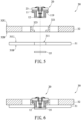
- Fig. 5 illustrates an exploded cross-sectional view of a probe card according to an exemplary embodiment of the instant disclosure.
- Fig. 6 illustrates an assembled cross-sectional view of the probe card of the exemplary embodiment.
- Fig. 7 illustrates a schematic view showing the switch module of the probe card of the exemplary embodiment is electrically connected to the test circuit board.
- Fig. 8 illustrates a top schematic view of the probe card of the exemplary embodiment.
- the probe card 30 comprises a test circuit board 31, a reinforcement member 32, a switch module 20, and a test head 35.
- the test circuit board 31 comprises an upper surface 31U, a bottom surface 31B, and a central hole 311.
- the upper surface 31U is defined as the tester side of the test circuit board 31; that is, a surface of the test circuit board 31 adapted to be connected to a test device.
- the lower surface 31B is defined as the wafer side of the test circuit board 31; that is, a surface of the test circuit board 31 facing the wafer to be tested.
- the reinforcement member 32 may be a frame made of aluminum or aluminum alloy.
- the reinforcement member 32 is disposed on the upper surface 31U of the test circuit board 31 so as to improve the stiffness of the test circuit board 31.
- the reinforcement member 32 comprises a central carrier 321 disposed on a central portion thereof and the central carrier 321 corresponds to the central hole 311 of the test circuit board 31.
- the central carrier 321 is connected to a main body of the reinforcement member 32 with four bridging members 329.
- the central carrier 321 may be connected to the main body of the reinforcement member 32 just with two bridging members 321 or even with bridging members in other shapes, depending on the model number of the test circuit board 31.
- the switch module 20 Upon the assembly of the probe card 30, the switch module 20 is inserted into the central carrier 321 from an upper surface 32U of the reinforcement member 32, and the microhole plate 12 of the switch module 20 protrudes out of a lower surface 32B of the reinforcement member 32 and of the lower surface 31B of the test circuit board 31, and then the microhole plate 12 is electrically connected to the test head 35.
- an inner surface of the central carrier 321 has a flange 323, as shown in Fig. 5 .
- the outer diameter of the switch plate 23 may be as larger as possible, for example, the outer diameter of the switch plate 23 may be greater than a hole diameter of the central hole 311 of the test circuit board 31.
- a material of the wires 18 is different from a material of the intermediate circuit traces 27 and is also different from a material of the external circuit traces 37. Since the wire diameter of each of the wires 18 is not greater than 50 micrometers, e.g., may be 35 micrometer, the wires 18 may be broken easily when made of common metal lines.
- the material of the wires 18 may be a metal material which is not broken easily under the wire diameter requirement.
- the wires 18 may be made of copper-tungsten alloy or copper-silver alloy, or may be made of the aforementioned alloys doped with rhenium, palladium, or beryllium.
- a ratio of a length of a longest wire of the wires 18 and a length of a shortest wire of the wires 18 is less than 1.1.
- the lengths of the wires 18 are configured to be maintained in a uniform length as much as possible; even if the wires 18 have different lengths, the length of the longest wire cannot exceed the length of the shortest wire by 10% of the length of the shortest wire.
- a sealing glue e.g., epoxy resin
Landscapes
- Engineering & Computer Science (AREA)
- Power Engineering (AREA)
- Physics & Mathematics (AREA)
- General Physics & Mathematics (AREA)
- Measuring Leads Or Probes (AREA)
- Testing Or Measuring Of Semiconductors Or The Like (AREA)
Description
- The instant disclosure relates to a probe card and a switch module.
- A manufacturing method for integrated circuit (IC) chips includes forming several dies on a wafer, cutting the wafer into several independent dies, and then packaging the dies individually. The dies with different functions may have different sizes. For a die with complicated functions, the size of the die is larger, and the number of contact points on the larger-sized die is more. As a result, the distance between the contact points of the large-sized die is quite narrow. On the other hand, though the number of the contact points on the die with simple functions is lesser, the distance between the contact points of the die with simple functions is still narrow due to the die having a smaller size. Consequently, the dies may perform electrical connections with the circuit board hardly.
- To allow the circuits in the dies to be electrically connected to the circuit board, the spatial distribution of the contact points on the dies has to be enlarged, and the step is called space transform. The space transform step may be implemented by soldering the dies on an IC carrier plate. The IC carrier plate has an upper surface and a lower surface, the spatial distribution of upper contact points at the upper surface is the same as the spatial distribution of the contact points of corresponding dies; conversely, the spatial distribution of lower contact points at the lower surface is rather looser, with respect to the spatial distribution of the contact points of the corresponding dies. A circuit layout is configured between the upper surface and the lower surface, so that the upper contact points at the upper surface and the lower contact points at the lower surface are electrically connected to each other. Accordingly, the spatial distribution of the contact points of a die can be enlarged through the IC carrier plate.
- Before the dies are combined with the IC carrier plate, generally a testing procedure, e.g., probing with a probe card, is to apply to the dies. In order to detect the dies on the wafer, the probe distribution on the probe card has to be the same as the distribution of the contact points on the dies. As a result, the probes on the probe card are arranged in a dense configuration as well. As mentioned above, due to the dense configuration of the contact points on the dies, the direct electrical connection between the contact points on the dies and the circuit board may be difficult. Similarly, the same issue may occur to the dense-configured probes upon the probes are to be electrically connecting to a test circuit board directly. Consequently, "a spatial transform device" is to be provided for the probes, so that the spatial transform step for the probes can be implemented and then the probes are electrically connected to the test circuit board.
- The spatial transform device, similar to the IC carrier, has a top surface and a bottom surface. The distribution of contact points at the bottom surface for connecting to the probes is the same as the dense distribution of the contact points of the probes; conversely, the distribution of contact points at the top surface facing the test circuit board is rather looser, with respect to the distribution of the contact points of the probes.
-
US2012146677A discloses a probe card that facilitates a wiring connection, reducing
working time and preventing a working error and includes a main circuit board having an opening in its center. A reinforcement member has a lower end coupled to that opening to prevent deforming of the board. A sub-circuit board electrically connected to the main board is seated on an upper side of the reinforcement member. A space transformer is positioned on a lower portion of the opening of the main board. A plurality of wires have both ends inserted into through holes in the sub-circuit board and space transformer to electrically connect them. Probes are provided on a lower portion of the space transformer, each having one end in contact with the wire inserted into the through-hole of the space transformer and the other end in contact with a wafer to be tested. -
US2016109483A1 discloses an electrical contacting device for electrical physical contact with a specimen, particularly wafers, taking place in a contacting direction, with at least one conductor substrate which can be electrically connected to a testing device, at least one contact distance transformer and at least one contact head having electrical contact elements, particularly resilient contact elements, preferably serving to compensate different physical contact distances existing in the contacting direction particularly at the contact elements. -
US 2004207420A1 discloses a modularized probe card with a coaxial transmitter. At least a coaxial transmitter is modularized and installed between a first printed circuit board and a second printed circuit board. The coaxial transmitter has a first connector and a second connector correspondingly connecting two ends of each coaxial cable of the coaxial transmitter for electrically connecting corresponding in location to first printed circuit board and second printed circuit board. A probe head is bonded on second printed circuit board. The second connector of the coaxial transmitter is connected with the second printed circuit board in a plug-in and pull-away type. - In a spatial transform device known to the inventor, the microhole plate is directly wired to the test circuit board when the spatial transform device is to be electrically connected to the test circuit board. As a result, the wire traces are intersected with each other, thereby causing the interferences between the signals in the wires easily. Moreover, since the lengths of the wires are different, the signals in the wires have different time sequences, thereby affecting the accuracy of the result for electrical testing.
- In view of these, one embodiment of the instant disclosure provides a switch module according to claim 1.
- Accordingly, the switch module is adapted to be electrically connected to a corresponding test circuit board through the switch plate, so that the wires are not intersected with each other and have a uniform length. Hence, the problem of interferences between signals in different wires and the problem of test signals with different time sequences as mentioned above can be improved.
- The disclosure will become more fully understood from the detailed description given herein below for illustration only, and thus not limitative of the disclosure, wherein:
-
Fig. 1 illustrates an exploded cross-sectional view of a switch module according to an example not according to the claimed invention; -
Fig. 2 illustrates an assembled cross-sectional view of the switch module of the example; -
Fig. 3 illustrates an assembled cross-sectional view of a switch module according to an exemplary embodiment of the instant disclosure, where the switch module has a positioning film and an inner layer circuit layout; -
Fig. 4 illustrates an assembled cross-sectional view of a switch module according to further another exemplary embodiment of the instant disclosure, where the switch module has a positioning film and external circuit traces; -
Fig. 5 illustrates an exploded cross-sectional view of a probe card according to an exemplary embodiment of the instant disclosure; -
Fig. 6 illustrates an assembled cross-sectional view of the probe card of the exemplary embodiment; -
Fig. 7 illustrates a schematic view showing the switch module of the probe card of the exemplary embodiment is electrically connected to the test circuit board; and -
Fig. 8 illustrates a top schematic view of the probe card of the exemplary embodiment. - Please refer to
Figs. 1 and 2 , respectively illustrating an exploded cross-sectional view and an assembled cross-sectional view of a switch module according to an example not falling within the subject-matter of the claims. In one or more examples, theswitch module 10 comprises abase 11, amicrohole plate 12, and aswitch plate 13. The material of thebase 11, in general, may be stainless steel, and a center portion of thebase 11 has ahollow portion 111. The material of themicrohole plate 12, in general, may be ceramic materials, and themicrohole plate 12 is disposed below thebase 11. Theswitch plate 13 may be a single-layered circuit board or a multilayered circuit board, and theswitch plate 13 is disposed above thebase 11. Themicrohole plate 12 comprises a plurality offirst microholes 121 facing thehollow portion 111 of thebase 11. Theswitch plate 13 comprises atop surface 13U and abottom surface 13B. Thebottom surface 13B faces thebase 11, and thetop surface 13U comprises a plurality ofupper contact points 131. - In some examples, the
switch plate 13 is not directly disposed on thebase 11; instead, theswitch plate 13 is disposed above thebase 11 usingsteel posts 139, so that an included angle between thewires 18 and theswitch plate 13 can be reduced, thereby reducing the bending angle of thewires 18. Hence, the reliability and the durability of the electrical connection between thewires 18 and theswitch plate 13 can be increased. In some examples, theswitch plate 13 comprises acentral region 13C and anedge region 13E surrounding thecentral region 13C, and theupper contact points 131 are in theedge region 13E. In some examples, theedge region 13E is defined as a region of theswitch plate 13 whose projection in the normal direction of theswitch plate 13 does not overlap with thehollow portion 111 of thebase 11. In some examples, theswitch plate 13 is of a circular shape and has a radius, thecentral region 13C is defined as a circular region from the center of circle of theswitch plate 13 to a length of 0.7 times of the radius of theswitch plate 13, and theedge region 13E is defined as an annular region of theswitch plate 13 out of the circular region. In some examples, the projection of thecentral region 13C in the normal direction of the surface of theswitch plate 13 is just overlapped with thehollow portion 111; in other words, in these examples, the periphery of the projection of thecentral region 13C is substantially aligned with the periphery of thehollow portion 111. It is understood that, in the case that the upper contact points 131 are configured in theedge region 13E of theswitch plate 13, that is, in the case that the upper contact points 131 are configured close to the periphery of theswitch plate 13, the electrical connection between the upper contact points 131 and a test circuit board which will be described in the following paragraphs can be facilitated. - As shown in
Fig. 3 , according to the invention, theswitch module 10 further comprises apositioning film 19. Thepositioning film 19 is used to guide thewires 18 passing through themicrohole plate 12 to be aligned orderly, so that the operator can determine the order for each of thewires 18. Thepositioning film 19 may be made of polymer materials and flexible. Thepositioning film 19 is disposed between themicrohole plate 12 and theswitch plate 13, and thepositioning film 19 is located above thefirst microholes 121 of themicrohole plate 12. In some embodiments, theswitch plate 13 further comprises an innerlayer circuit layout 13L located between thetop surface 13U and thebottom surface 13B. The innerlayer circuit layout 13L is used to allow thewires 18 to be electrically connected to the upper contact points 131 at thetop surface 13U through the innerlayer circuit layout 13L. Thepositioning film 19 comprises a plurality ofsecond microholes 191 respectively corresponding to thefirst microholes 121. Moreover, a distance between two adjacentsecond microholes 191 is equal to a distance between two adjacentfirst microholes 121. In other words, the segments of thewires 18 between thepositioning film 19 and themicrohole plate 12 do not have the fan-out layout yet; instead, the fan-out layout of thewires 18 starts from the segments of thewires 18 between thepositioning film 19 and thebottom surface 13B of theswitch plate 13. - As above, in this embodiment, after the
wires 18 pass through thepositioning film 19, thewires 18 extend to theswitch plate 13. The distance between twoadjacent wires 18 gradually becomes larger as the twoadjacent wires 18 get closer to thebottom surface 13B of theswitch plate 13. Next, thewires 18 further pass through thevias 132 of theswitch plate 13 and are soldered on thetop surface 13U of theswitch plate 13. A distance between twoadjacent vias 132 are fixed. In other words, if the distance between two adjacentfirst microholes 121 of themicrohole plate 12 is defined as P1, the distance between two adjacentsecond microholes 191 of thepositioning film 19 is defined as P2, and the distance between twoadjacent vias 132 of theswitch plate 13 is defined as P3, then P1=P2<P3, and a distance between twoadjacent wires 18 gradually approaches to reach P3, from the segments of thewires 18 at thepositioning film 19 to the segments of thewires 18 closer to theswitch plate 13. - During the installation of the
wires 18, firstly thepositioning film 19 is disposed on themicrohole plate 12, and thesecond microholes 191 and thefirst microholes 121 are aligned with each other in a one-by-one manner. Then, thewires 18 respectively pass through thesecond microholes 191 and respectively pass through thefirst microholes 121 from top to bottom. Hence, the segments of thewires 18 between thepositioning film 19 and themicrohole plate 12 are in a vertical configuration; namely, thewires 18 are of a linear configuration and do not have bent portions, so that thewires 18 are spaced with a fixed interval and do not intersect with each other. therefore, the electrical abnormality issue caused by the intersection of thewires 18 can be eliminated. Furthermore, thepositioning film 19 can be provided for arranging thewires 18, so that the operator can perform the subsequent electrical connection procedure in a convenient manner. After thewires 18 are arranged, a glue material (e.g., epoxy resin) may be applied to fill the space between thepositioning film 19 and themicrohole plate 12, so that the distance between thepositioning film 19 and themicrohole plate 12 can be fixed. Moreover, the segments of thewires 18 between thepositioning film 19 and themicrohole plate 12 can be spaced by the glue material, thereby further ensuring the segments of thewires 18 between thepositioning film 19 and themicrohole plate 12 not being intersected with each other. - As shown in
Fig. 4 , in some embodiments, theswitch plate 23 comprises a plurality of first upper contact points 231C and a plurality of secondupper contact points 231E electrically connected to the first upper contact points 231C, respectively. The first upper contact points 231C are in thecentral region 23C, and the second upper contact points 231E are in theedge region 23E. In some embodiments, theswitch plate 23 further comprises intermediate circuit traces 27. The intermediate circuit traces 27 are used to electrically connect the first upper contact points 231C to the second upper contact points 231E, respectively. Similarly, in these embodiments, the segments of thewires 18 between thepositioning film 19 and themicrohole plate 12, as shown inFig. 4 , do not have the fan-out layout; instead, the fan-out layout of thewires 18 starts from the segments of thewires 18 between thepositioning film 19 and thebottom surface 23B of theswitch plate 23. - In some embodiments, as shown in
Figs. 1 and 2 , a distance L between thebottom surface 13B of theswitch plate 13 and an upper surface off themicrohole plate 12 is greater than 4 mm. Because it is understood that, the thickness of a test circuit board is usually greater than 4 mm, the distance L between thebottom surface 13B of theswitch plate 13 and the upper surface of themicrohole plate 12 is configured to be greater than 4 mm, so that when theswitch module 10 is assembled with the test circuit board, thetop surface 13U of theswitch plate 13 can protrude out of the upper surface of the test circuit board, and themicrohole plate 12 can protrude out of the lower surface of the test circuit board. Moreover, in some embodiments, the ensemble of contact positions between thewires 18 and thebottom surface 13B of theswitch plate 13 forms a circular soldering region or a rectangular soldering region. A radius of the circular soldering region is defined as R, while a side length of the rectangular soldering region is defined as 2R. The distance between thebottom surface 13B of theswitch plate 13 and the upper surface of themicrohole plate 12 is defined as L, and a value of R/L is in a range between 0.1 and 7.5. In some embodiments, the distance L between thebottom surface 13B of theswitch plate 13 and the upper surface of themicrohole plate 12 is in a range between 4 mm to 40 mm, and the radius of the circular soldering region is in a range between 4 mm to 30 mm. - Please refer to
Figs. 5 to 8 .Fig. 5 illustrates an exploded cross-sectional view of a probe card according to an exemplary embodiment of the instant disclosure.Fig. 6 illustrates an assembled cross-sectional view of the probe card of the exemplary embodiment.Fig. 7 illustrates a schematic view showing the switch module of the probe card of the exemplary embodiment is electrically connected to the test circuit board.Fig. 8 illustrates a top schematic view of the probe card of the exemplary embodiment. In one or some embodiments, theprobe card 30 comprises atest circuit board 31, areinforcement member 32, aswitch module 20, and atest head 35. Thetest circuit board 31 comprises anupper surface 31U, abottom surface 31B, and acentral hole 311. Theupper surface 31U is defined as the tester side of thetest circuit board 31; that is, a surface of thetest circuit board 31 adapted to be connected to a test device. Thelower surface 31B is defined as the wafer side of thetest circuit board 31; that is, a surface of thetest circuit board 31 facing the wafer to be tested. Thereinforcement member 32 may be a frame made of aluminum or aluminum alloy. Thereinforcement member 32 is disposed on theupper surface 31U of thetest circuit board 31 so as to improve the stiffness of thetest circuit board 31. Thereinforcement member 32 comprises acentral carrier 321 disposed on a central portion thereof and thecentral carrier 321 corresponds to thecentral hole 311 of thetest circuit board 31. Moreover, thecentral carrier 321 is connected to a main body of thereinforcement member 32 with four bridgingmembers 329. In some embodiments, thecentral carrier 321 may be connected to the main body of thereinforcement member 32 just with two bridgingmembers 321 or even with bridging members in other shapes, depending on the model number of thetest circuit board 31. - Upon the assembly of the
probe card 30, theswitch module 20 is inserted into thecentral carrier 321 from anupper surface 32U of thereinforcement member 32, and themicrohole plate 12 of theswitch module 20 protrudes out of alower surface 32B of thereinforcement member 32 and of thelower surface 31B of thetest circuit board 31, and then themicrohole plate 12 is electrically connected to thetest head 35. In some embodiments, an inner surface of thecentral carrier 321 has aflange 323, as shown inFig. 5 . When theswitch module 20 is received in thecentral carrier 321, theflange 323 abuts against anouter periphery 119 of thebase 11. Therefore, the movement of theswitch module 20 is limited by theflange 323 and cannot further pass through thereinforcement member 32 from top to bottom in a vertical direction. - In some embodiments, the outer diameter of the
switch plate 23 may be as larger as possible, for example, the outer diameter of theswitch plate 23 may be greater than a hole diameter of thecentral hole 311 of thetest circuit board 31. - In some embodiments, a material of the
wires 18 is different from a material of the intermediate circuit traces 27 and is also different from a material of the external circuit traces 37. Since the wire diameter of each of thewires 18 is not greater than 50 micrometers, e.g., may be 35 micrometer, thewires 18 may be broken easily when made of common metal lines. The material of thewires 18 may be a metal material which is not broken easily under the wire diameter requirement. For example, thewires 18 may be made of copper-tungsten alloy or copper-silver alloy, or may be made of the aforementioned alloys doped with rhenium, palladium, or beryllium. Since the wire diameter of each of thewires 18 is quite small and thewires 18 are arranged densely, thewires 18 can be arranged properly through the configuration of thepositioning film 19, so that operators can perform the procedures conveniently. In some embodiments, a ratio of a length of a longest wire of thewires 18 and a length of a shortest wire of thewires 18 is less than 1.1. In other words, substantially, the lengths of thewires 18 are configured to be maintained in a uniform length as much as possible; even if thewires 18 have different lengths, the length of the longest wire cannot exceed the length of the shortest wire by 10% of the length of the shortest wire. Moreover, a sealing glue (e.g., epoxy resin) may be filled in the space between themicrohole plate 12 and theswitch plate 13 to seal thewires 18 so as to protect thewires 18, thereby improving the weatherability of the entire switch module. - It is understood that, in order to explain the structures of the switch module and the probe card conveniently, the elements in the drawings are not illustrated to actual scale.
- While the instant disclosure has been described by the way of example and in terms of the preferred embodiments, it is to be understood that the invention need not be limited to the disclosed embodiments.
Claims (14)
- A switch module (10, 20) adapted to be electrically connecting a plurality of probes of a test head (35) to a plurality of upper contact points of an upper surface (31U) of a test circuit board (31), wherein the switch module (10, 20) comprises:a base (11) comprising a hollow portion (111);a microhole plate (12) disposed below the base (11), wherein the microhole plate (12) comprises a plurality of first microholes (121) facing the hollow portion (111);a switch plate (13, 23) disposed above the base (11), wherein an outer diameter of the switch plate (13, 23) is greater than a hole size of the hollow portion (111), the switch plate (13, 23) comprises a top surface (13U), a bottom surface (13B), and a plurality of vias (132), the bottom surface (13B) of the switch plate (13, 23) faces the base (11), the top surface (13U) of the switch plate (13, 23) comprises a plurality of upper contact points (131), the vias (132) are extending from the top surface (13U) of the switch plate (13, 23) to the bottom surface (13B) of the switch plate (13, 23);a plurality of wires (18) respectively passing through the first microholes (121) of the microhole plate (12) and the vias (132) of the switch plate (13, 23), wherein the wires (18) electrically connect the microhole plate (12) to the upper contact points (131) of the top surface (13U) of the switch plate (13, 23);a plurality of external circuit traces (37) for respectively and electrically connecting the upper contact points (131) of the switch plate (13, 23) to the upper contact points of the upper surface (31U) of the test circuit board (31); andwherein a distance between two adjacent vias (132) of the switch plate (13, 23) is greater than a distance between two adjacent first microholes (121) of the microhole plate (12), and a ratio of a length of a longest wire of the wires (18) and a length of a shortest wire of the wires (18) is less than 1.1; characterised in that the switch module (10,20) further comprises:
a positioning film (19), disposed between the microhole plate (12) and the switch plate (13, 23) and above the first microholes (121) of the microhole plate (12), wherein the positioning film (19) comprises a plurality of second microholes (191) respectively corresponding to the first microholes (121), the wires (18) respectively pass through the second microholes (191) of the positioning film (19), a distance between two adjacent vias (132) of the switch plate (13, 23) is greater than a distance between two adjacent second microholes (191) of the positioning film (19), and the distance between two adjacent second microholes (191) of the positioning film (19) is equal to the distance between two adjacent first microholes (121) of the microhole plate (12). - The switch module (10) according to claim 1, wherein a distance between the top surface (13U) of the switch plate (13) and an upper surface of the microhole plate (12) is greater than 4 mm.
- The switch module (10) according to claim 1, wherein an ensemble of contact positions between the wires (18) and the bottom surface (13B) of the switch plate (13) forms a circular soldering region, a radius of the circular soldering region is defined as R, a distance between the bottom surface (13B) of the switch plate (13) and an upper surface of the microhole plate (12) is defined as L, and a value of R/L is in a range between 0.1 and 7.5.
- The switch module (10) according to claim 1, wherein an ensemble of contact positions between the wires (18) and the bottom surface (13B) of the switch plate (13) forms a rectangular soldering region, a side length of the rectangular soldering region is defined as 2R, a distance between the bottom surface (13B) of the switch plate (13) and an upper surface of the microhole plate (12) is defined as L, and a value of R/L is in a range between 0.1 and 7.5.
- A probe card (30) comprising:a test circuit board (31) comprising an upper surface (3 1U), a lower surface (31B), and a central hole (311);a reinforcement member (32) disposed on the upper surface (31U) of the test circuit board (31), wherein the reinforcement member (32) comprises a central carrier (321) corresponding to the central hole (311);a switch module (10, 20) according to any one of claims 1 to 5, wherein the switch module (10, 20) is received in the central carrier (321) of the reinforcement member (32), and wherein the wires (18) do not intersect with each other and have a uniform length
- The probe card (30) according to claim 5, wherein the switch plate (13, 23) comprises a central region (13C, 23C) and an edge region (13E, 23E) surrounding the central region (13C, 23E), and the upper contact points (131) are in the edge region (13E, 23E).
- The probe card (30) according to claim 6, wherein a projection of the edge region (13E, 23E) in a normal direction of the switch plate is not overlapped with the hollow portion (111) of the base (11).
- The probe card (30) according to claim 7, wherein the switch plate (13, 23) further comprises an inner layer circuit layout (13L) located between the top surface (13U) and the bottom surface (13B), the wires (18) are electrically connected to the upper contact points (131) of the switch plate (13, 23) through the inner layer circuit layout (13L).
- The probe card (30) according to claim 6, wherein the switch module (10, 20) further comprises a plurality of intermediate circuit traces (27), the switch plate (13, 23) further comprises a central region (13C, 23C) and an edge region (13E, 23E) surrounding the central region (13C, 23C); the upper contact points of the switch plate (13, 23) are divided into a plurality of first upper contact points (231C) and a plurality of second upper contact points (231E), the first upper contact points (231C) are in the central region (13C, 23C), and the second upper contact points (13E, 231E) are in the edge region (13E, 23E); the wires (18) electrically connect the microhole plate (12) to the first upper contact points (231C) of the switch plate (13, 23), and the intermediate circuit traces (27) electrically connect the first upper contact points (231C) to the second upper contact points (231E).
- The probe card (30) according to claim 6, wherein a projection of the edge region (13E, 23E) in a normal direction of the switch plate is not overlapped with the hollow portion (111) of the base (11).
- The probe card (30) according to claim 6, wherein a material of the wires (18) is different from a material of the external circuit traces (37) and is different from a material of the intermediate circuit traces (13L).
- The probe card (30) according to claim 5, wherein an inner surface of the central carrier (321) has a flange (323) abutted against an outer periphery (119) of the base (11).
- The probe card (30) according to claim 5, wherein the microhole plate (12) is exposed from the lower surface (31B) of the test circuit board (31).
- The probe card (30) according to claim 5, wherein an outer diameter of the switch plate (13, 23) is greater than a hole diameter of the central hole (311) of the test circuit board (31).
Applications Claiming Priority (2)
| Application Number | Priority Date | Filing Date | Title |
|---|---|---|---|
| TW108119092 | 2019-05-31 | ||
| TW108144391A TWI712800B (en) | 2019-05-31 | 2019-12-04 | Probe card and switch module |
Publications (2)
| Publication Number | Publication Date |
|---|---|
| EP3745142A1 EP3745142A1 (en) | 2020-12-02 |
| EP3745142B1 true EP3745142B1 (en) | 2023-10-04 |
Family
ID=70289678
Family Applications (1)
| Application Number | Title | Priority Date | Filing Date |
|---|---|---|---|
| EP20169599.6A Active EP3745142B1 (en) | 2019-05-31 | 2020-04-15 | Probe card and switch module |
Country Status (2)
| Country | Link |
|---|---|
| EP (1) | EP3745142B1 (en) |
| CN (1) | CN112017981B (en) |
Families Citing this family (1)
| Publication number | Priority date | Publication date | Assignee | Title |
|---|---|---|---|---|
| CN115542116A (en) * | 2022-09-21 | 2022-12-30 | 中国电子产品可靠性与环境试验研究所((工业和信息化部电子第五研究所)(中国赛宝实验室)) | Printed circuit board test system, method, device, equipment and storage medium |
Family Cites Families (8)
| Publication number | Priority date | Publication date | Assignee | Title |
|---|---|---|---|---|
| US6812720B1 (en) * | 2003-04-17 | 2004-11-02 | Chipmos Technologies (Bermuda) Ltd. | Modularized probe card with coaxial transmitters |
| US7368928B2 (en) * | 2006-08-29 | 2008-05-06 | Mjc Probe Incorporation | Vertical type high frequency probe card |
| US7733102B2 (en) * | 2007-07-10 | 2010-06-08 | Taiwan Semiconductor Manufacturing Company, Ltd. | Ultra-fine area array pitch probe card |
| KR100996927B1 (en) * | 2008-10-28 | 2010-11-26 | 윌테크놀러지(주) | Spatial transducers and probe cards containing them |
| KR101047537B1 (en) * | 2010-12-08 | 2011-07-08 | 주식회사 에스디에이 | Probe card |
| DE102013008324A1 (en) * | 2013-05-08 | 2014-11-13 | Feinmetall Gmbh | Electrical contacting device |
| TW201623976A (en) * | 2014-12-24 | 2016-07-01 | Mpi Corp | Vertical probe device with positioning plates |
| WO2018182719A1 (en) * | 2017-03-31 | 2018-10-04 | Intel Corporation | Ultra low-cost, low leadtime, and high density space transformer for fine pitch applications |
-
2020
- 2020-03-30 CN CN202010235672.6A patent/CN112017981B/en active Active
- 2020-04-15 EP EP20169599.6A patent/EP3745142B1/en active Active
Also Published As
| Publication number | Publication date |
|---|---|
| EP3745142A1 (en) | 2020-12-02 |
| CN112017981B (en) | 2025-01-21 |
| CN112017981A (en) | 2020-12-01 |
Similar Documents
| Publication | Publication Date | Title |
|---|---|---|
| KR100847034B1 (en) | Contactor and manufacturing method thereof | |
| US8427186B2 (en) | Probe element having a substantially zero stiffness and applications thereof | |
| JP2014508944A (en) | Equipment for automatic testing / verification of electronic components | |
| US20080048689A1 (en) | Wafer type probe card, method for fabricating the same, and semiconductor test apparatus having the same | |
| JP2009526992A (en) | Space transformer, manufacturing method of the space transformer, and probe card having the space transformer | |
| US20080218188A1 (en) | Jig for printed substrate inspection and printed substrate inspection apparatus | |
| JP2009541715A (en) | Sewing the corner of the tile on the probe card board | |
| US7825410B2 (en) | Semiconductor device | |
| WO2020179596A1 (en) | Electrical connection apparatus | |
| US6255832B1 (en) | Flexible wafer level probe | |
| US7948253B2 (en) | Probe assembly | |
| KR101811859B1 (en) | Probe card | |
| JP2018159690A (en) | Electrical connection device | |
| EP3745142A1 (en) | Probe card and switch module | |
| KR101104290B1 (en) | Mounting method of contactor | |
| US20020175695A1 (en) | Micro probing techniques for testing electronic assemblies | |
| US7456640B2 (en) | Structure for coupling probes of probe device to corresponding electrical contacts on product substrate | |
| US11209462B1 (en) | Testing apparatus | |
| US6407568B1 (en) | Apparatus for probing ends of pins | |
| TWI712800B (en) | Probe card and switch module | |
| US20030094962A1 (en) | Dual plane probe card assembly and method of manufacture | |
| EP0654672B1 (en) | Integrated circuit test apparatus | |
| US8476919B2 (en) | Prober unit | |
| US20250147073A1 (en) | Probe card and method for design probe card and measuring method and system for detecting device under test using the probe card | |
| KR101106607B1 (en) | Test device for semiconductor device |
Legal Events
| Date | Code | Title | Description |
|---|---|---|---|
| PUAI | Public reference made under article 153(3) epc to a published international application that has entered the european phase |
Free format text: ORIGINAL CODE: 0009012 |
|
| STAA | Information on the status of an ep patent application or granted ep patent |
Free format text: STATUS: THE APPLICATION HAS BEEN PUBLISHED |
|
| AK | Designated contracting states |
Kind code of ref document: A1 Designated state(s): AL AT BE BG CH CY CZ DE DK EE ES FI FR GB GR HR HU IE IS IT LI LT LU LV MC MK MT NL NO PL PT RO RS SE SI SK SM TR |
|
| AX | Request for extension of the european patent |
Extension state: BA ME |
|
| STAA | Information on the status of an ep patent application or granted ep patent |
Free format text: STATUS: REQUEST FOR EXAMINATION WAS MADE |
|
| 17P | Request for examination filed |
Effective date: 20210602 |
|
| RBV | Designated contracting states (corrected) |
Designated state(s): AL AT BE BG CH CY CZ DE DK EE ES FI FR GB GR HR HU IE IS IT LI LT LU LV MC MK MT NL NO PL PT RO RS SE SI SK SM TR |
|
| GRAP | Despatch of communication of intention to grant a patent |
Free format text: ORIGINAL CODE: EPIDOSNIGR1 |
|
| STAA | Information on the status of an ep patent application or granted ep patent |
Free format text: STATUS: GRANT OF PATENT IS INTENDED |
|
| INTG | Intention to grant announced |
Effective date: 20230420 |
|
| GRAS | Grant fee paid |
Free format text: ORIGINAL CODE: EPIDOSNIGR3 |
|
| GRAA | (expected) grant |
Free format text: ORIGINAL CODE: 0009210 |
|
| STAA | Information on the status of an ep patent application or granted ep patent |
Free format text: STATUS: THE PATENT HAS BEEN GRANTED |
|
| AK | Designated contracting states |
Kind code of ref document: B1 Designated state(s): AL AT BE BG CH CY CZ DE DK EE ES FI FR GB GR HR HU IE IS IT LI LT LU LV MC MK MT NL NO PL PT RO RS SE SI SK SM TR |
|
| REG | Reference to a national code |
Ref country code: GB Ref legal event code: FG4D |
|
| REG | Reference to a national code |
Ref country code: CH Ref legal event code: EP |
|
| REG | Reference to a national code |
Ref country code: IE Ref legal event code: FG4D |
|
| REG | Reference to a national code |
Ref country code: DE Ref legal event code: R096 Ref document number: 602020018477 Country of ref document: DE |
|
| REG | Reference to a national code |
Ref country code: LT Ref legal event code: MG9D |
|
| REG | Reference to a national code |
Ref country code: NL Ref legal event code: MP Effective date: 20231004 |
|
| REG | Reference to a national code |
Ref country code: AT Ref legal event code: MK05 Ref document number: 1618249 Country of ref document: AT Kind code of ref document: T Effective date: 20231004 |
|
| PG25 | Lapsed in a contracting state [announced via postgrant information from national office to epo] |
Ref country code: NL Free format text: LAPSE BECAUSE OF FAILURE TO SUBMIT A TRANSLATION OF THE DESCRIPTION OR TO PAY THE FEE WITHIN THE PRESCRIBED TIME-LIMIT Effective date: 20231004 |
|
| PG25 | Lapsed in a contracting state [announced via postgrant information from national office to epo] |
Ref country code: GR Free format text: LAPSE BECAUSE OF FAILURE TO SUBMIT A TRANSLATION OF THE DESCRIPTION OR TO PAY THE FEE WITHIN THE PRESCRIBED TIME-LIMIT Effective date: 20240105 |
|
| PG25 | Lapsed in a contracting state [announced via postgrant information from national office to epo] |
Ref country code: IS Free format text: LAPSE BECAUSE OF FAILURE TO SUBMIT A TRANSLATION OF THE DESCRIPTION OR TO PAY THE FEE WITHIN THE PRESCRIBED TIME-LIMIT Effective date: 20240204 |
|
| PG25 | Lapsed in a contracting state [announced via postgrant information from national office to epo] |
Ref country code: LT Free format text: LAPSE BECAUSE OF FAILURE TO SUBMIT A TRANSLATION OF THE DESCRIPTION OR TO PAY THE FEE WITHIN THE PRESCRIBED TIME-LIMIT Effective date: 20231004 |
|
| PG25 | Lapsed in a contracting state [announced via postgrant information from national office to epo] |
Ref country code: AT Free format text: LAPSE BECAUSE OF FAILURE TO SUBMIT A TRANSLATION OF THE DESCRIPTION OR TO PAY THE FEE WITHIN THE PRESCRIBED TIME-LIMIT Effective date: 20231004 |
|
| PG25 | Lapsed in a contracting state [announced via postgrant information from national office to epo] |
Ref country code: ES Free format text: LAPSE BECAUSE OF FAILURE TO SUBMIT A TRANSLATION OF THE DESCRIPTION OR TO PAY THE FEE WITHIN THE PRESCRIBED TIME-LIMIT Effective date: 20231004 |
|
| PG25 | Lapsed in a contracting state [announced via postgrant information from national office to epo] |
Ref country code: LT Free format text: LAPSE BECAUSE OF FAILURE TO SUBMIT A TRANSLATION OF THE DESCRIPTION OR TO PAY THE FEE WITHIN THE PRESCRIBED TIME-LIMIT Effective date: 20231004 Ref country code: IS Free format text: LAPSE BECAUSE OF FAILURE TO SUBMIT A TRANSLATION OF THE DESCRIPTION OR TO PAY THE FEE WITHIN THE PRESCRIBED TIME-LIMIT Effective date: 20240204 Ref country code: GR Free format text: LAPSE BECAUSE OF FAILURE TO SUBMIT A TRANSLATION OF THE DESCRIPTION OR TO PAY THE FEE WITHIN THE PRESCRIBED TIME-LIMIT Effective date: 20240105 Ref country code: ES Free format text: LAPSE BECAUSE OF FAILURE TO SUBMIT A TRANSLATION OF THE DESCRIPTION OR TO PAY THE FEE WITHIN THE PRESCRIBED TIME-LIMIT Effective date: 20231004 Ref country code: BG Free format text: LAPSE BECAUSE OF FAILURE TO SUBMIT A TRANSLATION OF THE DESCRIPTION OR TO PAY THE FEE WITHIN THE PRESCRIBED TIME-LIMIT Effective date: 20240104 Ref country code: AT Free format text: LAPSE BECAUSE OF FAILURE TO SUBMIT A TRANSLATION OF THE DESCRIPTION OR TO PAY THE FEE WITHIN THE PRESCRIBED TIME-LIMIT Effective date: 20231004 Ref country code: PT Free format text: LAPSE BECAUSE OF FAILURE TO SUBMIT A TRANSLATION OF THE DESCRIPTION OR TO PAY THE FEE WITHIN THE PRESCRIBED TIME-LIMIT Effective date: 20240205 |
|
| PG25 | Lapsed in a contracting state [announced via postgrant information from national office to epo] |
Ref country code: SE Free format text: LAPSE BECAUSE OF FAILURE TO SUBMIT A TRANSLATION OF THE DESCRIPTION OR TO PAY THE FEE WITHIN THE PRESCRIBED TIME-LIMIT Effective date: 20231004 Ref country code: RS Free format text: LAPSE BECAUSE OF FAILURE TO SUBMIT A TRANSLATION OF THE DESCRIPTION OR TO PAY THE FEE WITHIN THE PRESCRIBED TIME-LIMIT Effective date: 20231004 Ref country code: PL Free format text: LAPSE BECAUSE OF FAILURE TO SUBMIT A TRANSLATION OF THE DESCRIPTION OR TO PAY THE FEE WITHIN THE PRESCRIBED TIME-LIMIT Effective date: 20231004 Ref country code: NO Free format text: LAPSE BECAUSE OF FAILURE TO SUBMIT A TRANSLATION OF THE DESCRIPTION OR TO PAY THE FEE WITHIN THE PRESCRIBED TIME-LIMIT Effective date: 20240104 Ref country code: LV Free format text: LAPSE BECAUSE OF FAILURE TO SUBMIT A TRANSLATION OF THE DESCRIPTION OR TO PAY THE FEE WITHIN THE PRESCRIBED TIME-LIMIT Effective date: 20231004 Ref country code: HR Free format text: LAPSE BECAUSE OF FAILURE TO SUBMIT A TRANSLATION OF THE DESCRIPTION OR TO PAY THE FEE WITHIN THE PRESCRIBED TIME-LIMIT Effective date: 20231004 |
|
| REG | Reference to a national code |
Ref country code: DE Ref legal event code: R097 Ref document number: 602020018477 Country of ref document: DE |
|
| PG25 | Lapsed in a contracting state [announced via postgrant information from national office to epo] |
Ref country code: DK Free format text: LAPSE BECAUSE OF FAILURE TO SUBMIT A TRANSLATION OF THE DESCRIPTION OR TO PAY THE FEE WITHIN THE PRESCRIBED TIME-LIMIT Effective date: 20231004 |
|
| PG25 | Lapsed in a contracting state [announced via postgrant information from national office to epo] |
Ref country code: CZ Free format text: LAPSE BECAUSE OF FAILURE TO SUBMIT A TRANSLATION OF THE DESCRIPTION OR TO PAY THE FEE WITHIN THE PRESCRIBED TIME-LIMIT Effective date: 20231004 |
|
| PG25 | Lapsed in a contracting state [announced via postgrant information from national office to epo] |
Ref country code: SK Free format text: LAPSE BECAUSE OF FAILURE TO SUBMIT A TRANSLATION OF THE DESCRIPTION OR TO PAY THE FEE WITHIN THE PRESCRIBED TIME-LIMIT Effective date: 20231004 |
|
| PG25 | Lapsed in a contracting state [announced via postgrant information from national office to epo] |
Ref country code: SM Free format text: LAPSE BECAUSE OF FAILURE TO SUBMIT A TRANSLATION OF THE DESCRIPTION OR TO PAY THE FEE WITHIN THE PRESCRIBED TIME-LIMIT Effective date: 20231004 Ref country code: SK Free format text: LAPSE BECAUSE OF FAILURE TO SUBMIT A TRANSLATION OF THE DESCRIPTION OR TO PAY THE FEE WITHIN THE PRESCRIBED TIME-LIMIT Effective date: 20231004 Ref country code: RO Free format text: LAPSE BECAUSE OF FAILURE TO SUBMIT A TRANSLATION OF THE DESCRIPTION OR TO PAY THE FEE WITHIN THE PRESCRIBED TIME-LIMIT Effective date: 20231004 Ref country code: IT Free format text: LAPSE BECAUSE OF FAILURE TO SUBMIT A TRANSLATION OF THE DESCRIPTION OR TO PAY THE FEE WITHIN THE PRESCRIBED TIME-LIMIT Effective date: 20231004 Ref country code: EE Free format text: LAPSE BECAUSE OF FAILURE TO SUBMIT A TRANSLATION OF THE DESCRIPTION OR TO PAY THE FEE WITHIN THE PRESCRIBED TIME-LIMIT Effective date: 20231004 Ref country code: DK Free format text: LAPSE BECAUSE OF FAILURE TO SUBMIT A TRANSLATION OF THE DESCRIPTION OR TO PAY THE FEE WITHIN THE PRESCRIBED TIME-LIMIT Effective date: 20231004 Ref country code: CZ Free format text: LAPSE BECAUSE OF FAILURE TO SUBMIT A TRANSLATION OF THE DESCRIPTION OR TO PAY THE FEE WITHIN THE PRESCRIBED TIME-LIMIT Effective date: 20231004 |
|
| PLBE | No opposition filed within time limit |
Free format text: ORIGINAL CODE: 0009261 |
|
| STAA | Information on the status of an ep patent application or granted ep patent |
Free format text: STATUS: NO OPPOSITION FILED WITHIN TIME LIMIT |
|
| 26N | No opposition filed |
Effective date: 20240705 |
|
| PG25 | Lapsed in a contracting state [announced via postgrant information from national office to epo] |
Ref country code: SI Free format text: LAPSE BECAUSE OF FAILURE TO SUBMIT A TRANSLATION OF THE DESCRIPTION OR TO PAY THE FEE WITHIN THE PRESCRIBED TIME-LIMIT Effective date: 20231004 |
|
| PG25 | Lapsed in a contracting state [announced via postgrant information from national office to epo] |
Ref country code: SI Free format text: LAPSE BECAUSE OF FAILURE TO SUBMIT A TRANSLATION OF THE DESCRIPTION OR TO PAY THE FEE WITHIN THE PRESCRIBED TIME-LIMIT Effective date: 20231004 |
|
| PG25 | Lapsed in a contracting state [announced via postgrant information from national office to epo] |
Ref country code: MC Free format text: LAPSE BECAUSE OF FAILURE TO SUBMIT A TRANSLATION OF THE DESCRIPTION OR TO PAY THE FEE WITHIN THE PRESCRIBED TIME-LIMIT Effective date: 20231004 |
|
| PG25 | Lapsed in a contracting state [announced via postgrant information from national office to epo] |
Ref country code: MC Free format text: LAPSE BECAUSE OF FAILURE TO SUBMIT A TRANSLATION OF THE DESCRIPTION OR TO PAY THE FEE WITHIN THE PRESCRIBED TIME-LIMIT Effective date: 20231004 |
|
| REG | Reference to a national code |
Ref country code: CH Ref legal event code: PL |
|
| PG25 | Lapsed in a contracting state [announced via postgrant information from national office to epo] |
Ref country code: LU Free format text: LAPSE BECAUSE OF NON-PAYMENT OF DUE FEES Effective date: 20240415 |
|
| GBPC | Gb: european patent ceased through non-payment of renewal fee |
Effective date: 20240415 |
|
| REG | Reference to a national code |
Ref country code: BE Ref legal event code: MM Effective date: 20240430 |
|
| PG25 | Lapsed in a contracting state [announced via postgrant information from national office to epo] |
Ref country code: LU Free format text: LAPSE BECAUSE OF NON-PAYMENT OF DUE FEES Effective date: 20240415 |
|
| PG25 | Lapsed in a contracting state [announced via postgrant information from national office to epo] |
Ref country code: BE Free format text: LAPSE BECAUSE OF NON-PAYMENT OF DUE FEES Effective date: 20240430 |
|
| PG25 | Lapsed in a contracting state [announced via postgrant information from national office to epo] |
Ref country code: GB Free format text: LAPSE BECAUSE OF NON-PAYMENT OF DUE FEES Effective date: 20240415 |
|
| PG25 | Lapsed in a contracting state [announced via postgrant information from national office to epo] |
Ref country code: FR Free format text: LAPSE BECAUSE OF NON-PAYMENT OF DUE FEES Effective date: 20240430 |
|
| PG25 | Lapsed in a contracting state [announced via postgrant information from national office to epo] |
Ref country code: GB Free format text: LAPSE BECAUSE OF NON-PAYMENT OF DUE FEES Effective date: 20240415 Ref country code: FR Free format text: LAPSE BECAUSE OF NON-PAYMENT OF DUE FEES Effective date: 20240430 Ref country code: BE Free format text: LAPSE BECAUSE OF NON-PAYMENT OF DUE FEES Effective date: 20240430 Ref country code: CH Free format text: LAPSE BECAUSE OF NON-PAYMENT OF DUE FEES Effective date: 20240430 |
|
| PG25 | Lapsed in a contracting state [announced via postgrant information from national office to epo] |
Ref country code: IE Free format text: LAPSE BECAUSE OF NON-PAYMENT OF DUE FEES Effective date: 20240415 |
|
| PGFP | Annual fee paid to national office [announced via postgrant information from national office to epo] |
Ref country code: DE Payment date: 20250303 Year of fee payment: 6 |
|
| PG25 | Lapsed in a contracting state [announced via postgrant information from national office to epo] |
Ref country code: CY Free format text: LAPSE BECAUSE OF FAILURE TO SUBMIT A TRANSLATION OF THE DESCRIPTION OR TO PAY THE FEE WITHIN THE PRESCRIBED TIME-LIMIT; INVALID AB INITIO Effective date: 20200415 |
|
| PG25 | Lapsed in a contracting state [announced via postgrant information from national office to epo] |
Ref country code: HU Free format text: LAPSE BECAUSE OF FAILURE TO SUBMIT A TRANSLATION OF THE DESCRIPTION OR TO PAY THE FEE WITHIN THE PRESCRIBED TIME-LIMIT; INVALID AB INITIO Effective date: 20200415 |
|
| PG25 | Lapsed in a contracting state [announced via postgrant information from national office to epo] |
Ref country code: FI Free format text: LAPSE BECAUSE OF FAILURE TO SUBMIT A TRANSLATION OF THE DESCRIPTION OR TO PAY THE FEE WITHIN THE PRESCRIBED TIME-LIMIT Effective date: 20231004 |