EP3744001B1 - Systems and methods for coupling a superconducting transmission line to an array of resonators - Google Patents
Systems and methods for coupling a superconducting transmission line to an array of resonators Download PDFInfo
- Publication number
- EP3744001B1 EP3744001B1 EP19760892.0A EP19760892A EP3744001B1 EP 3744001 B1 EP3744001 B1 EP 3744001B1 EP 19760892 A EP19760892 A EP 19760892A EP 3744001 B1 EP3744001 B1 EP 3744001B1
- Authority
- EP
- European Patent Office
- Prior art keywords
- superconducting
- resonator
- transmission line
- inductance
- squid
- Prior art date
- Legal status (The legal status is an assumption and is not a legal conclusion. Google has not performed a legal analysis and makes no representation as to the accuracy of the status listed.)
- Active
Links
Images







Classifications
-
- H—ELECTRICITY
- H03—ELECTRONIC CIRCUITRY
- H03H—IMPEDANCE NETWORKS, e.g. RESONANT CIRCUITS; RESONATORS
- H03H2/00—Networks using elements or techniques not provided for in groups H03H3/00 - H03H21/00
- H03H2/005—Coupling circuits between transmission lines or antennas and transmitters, receivers or amplifiers
-
- B—PERFORMING OPERATIONS; TRANSPORTING
- B82—NANOTECHNOLOGY
- B82Y—SPECIFIC USES OR APPLICATIONS OF NANOSTRUCTURES; MEASUREMENT OR ANALYSIS OF NANOSTRUCTURES; MANUFACTURE OR TREATMENT OF NANOSTRUCTURES
- B82Y10/00—Nanotechnology for information processing, storage or transmission, e.g. quantum computing or single electron logic
-
- G—PHYSICS
- G06—COMPUTING OR CALCULATING; COUNTING
- G06N—COMPUTING ARRANGEMENTS BASED ON SPECIFIC COMPUTATIONAL MODELS
- G06N10/00—Quantum computing, i.e. information processing based on quantum-mechanical phenomena
-
- G—PHYSICS
- G06—COMPUTING OR CALCULATING; COUNTING
- G06N—COMPUTING ARRANGEMENTS BASED ON SPECIFIC COMPUTATIONAL MODELS
- G06N10/00—Quantum computing, i.e. information processing based on quantum-mechanical phenomena
- G06N10/40—Physical realisations or architectures of quantum processors or components for manipulating qubits, e.g. qubit coupling or qubit control
-
- H—ELECTRICITY
- H01—ELECTRIC ELEMENTS
- H01P—WAVEGUIDES; RESONATORS, LINES, OR OTHER DEVICES OF THE WAVEGUIDE TYPE
- H01P1/00—Auxiliary devices
- H01P1/20—Frequency-selective devices, e.g. filters
- H01P1/201—Filters for transverse electromagnetic waves
- H01P1/203—Strip line filters
- H01P1/20327—Electromagnetic interstage coupling
- H01P1/20354—Non-comb or non-interdigital filters
- H01P1/20381—Special shape resonators
-
- H—ELECTRICITY
- H03—ELECTRONIC CIRCUITRY
- H03H—IMPEDANCE NETWORKS, e.g. RESONANT CIRCUITS; RESONATORS
- H03H7/00—Multiple-port networks comprising only passive electrical elements as network components
- H03H7/38—Impedance-matching networks
- H03H7/383—Impedance-matching networks comprising distributed impedance elements together with lumped impedance elements
-
- H—ELECTRICITY
- H10—SEMICONDUCTOR DEVICES; ELECTRIC SOLID-STATE DEVICES NOT OTHERWISE PROVIDED FOR
- H10N—ELECTRIC SOLID-STATE DEVICES NOT OTHERWISE PROVIDED FOR
- H10N60/00—Superconducting devices
- H10N60/10—Junction-based devices
- H10N60/12—Josephson-effect devices
Definitions
- This disclosure generally relates to input and/or output systems and methods for superconducting devices such as superconducting quantum computers and superconducting classical computers, and, more specifically, to systems and methods for inputting data to a superconducting quantum processor and/or measuring the state of a qubit in the superconducting quantum processor.
- Superconducting microwave resonators have been used in a variety of fields including, but not limited to, quantum computation and astronomy. For example, in quantum computation, superconducting resonators have been used to detect the state of qubits. In astronomy, superconducting microwave resonators have been used in Microwave Kinetic Inductance Detectors (MKIDs). In both cases, many resonators (used as detectors or in detectors) can be coupled to a common transmission line and integrated through frequency domain multiplexing.
- Frequency domain multiplexing is a technique in which a communication bandwidth is divided into a number of non-overlapping sub-bands, each sub-band used to carry a separate signal.
- superconducting resonators of different resonant frequencies can be used for readout of multiple qubits.
- the resonators can share a common microwave transmission line by using frequency domain multiplexing.
- a frequency and sensitivity tunable microresonator array for high-speed quantum processor readout discloses a microresonator array for high-speed quantum processor readout.
- US 2016/0125309 A1 discloses quantum systems including a qubit and a transmission line resonator having an associated resonant wave-length.
- 2009/0289638 A1 discloses a method for determining whether a quantum system comprising a superconducting qubit is occupying a first basis state or a second basis state once a measurement is performed.
- US 5,153,171 discloses a superconducting variable phase shifter providing improved performance in the microwave and millimeter wave frequency ranges.
- US 2005/0184284 A1 discloses a method of coupling a qubit.
- Frequency Multiplexed Resonator (FMR) technology can be used to readout many single flux quanta simultaneously, and it has applications in both superconducting quantum computing and superconducting classical computing. FMR technology can also have applications in inputting data to a superconducting quantum processor, for example via a Quantum Flux Parametron (QFP) device. FMR technology can, for example, provide a scalable input/output technology.
- FMR Frequency Multiplexed Resonator
- the systems and methods described in the present application relate to aspects of FMR technology including a) the use an array of superconducting shunt-coupled resonators strongly coupled to a superconducting transmission line to perform high-speed readout, and b) approaches to at least partially compensate for transmission line impedance variations that can occur in the vicinity of the superconducting shunt-coupled resonators.
- a superconducting circuit is defined according to the claims.
- a qubit (also referred to in the present application as a quantum bit) is a basic unit of quantum information, and is a quantum version of a classical binary bit that can be physically realized with a two-state device.
- a qubit is a two-state quantum-mechanical system.
- a qubit also refers to the actual physical device in which information is stored.
- superconducting qubits are a type of superconducting device that can be included in a superconducting integrated circuit. Superconducting qubits can, for example, take the form of charged based or flux based qubits.
- a superconducting device is an electronic device that makes use of the properties of a superconducting material, for example zero electrical resistance and expulsion of magnetic flux when cooled below a critical temperature characteristic of the superconducting material.
- Microwave transmission line is a cable or other structure that includes one or more conductors operable to carry alternating electrical current of microwave frequency.
- a SQUID is a superconducting device that includes a superconducting loop containing one or more Josephson junctions.
- a SQUID can be used as a magnetometer able to measure very low magnetic fields.
- a DC SQUID has two Josephson junctions connected in parallel.
- An rf-SQUID has a superconducting loop containing a single Josephson junction.
- Lumped Element Design In a lumped element design, a spatially distributed physical system is described as a topology of discrete entities that approximate the behavior of the distributed system under certain assumptions. It is useful in electrical and electronic systems, for example.
- a shift register is a sequential logic circuit operable to store and/or transfer data.
- QFP Quantum Flux Parametron
- Hybrid Computer is a system that includes at least one digital processor, and at least one analog processor (e.g. a quantum processor).
- Ripple is an at least approximately periodic variation in signal. On a transmission line, for example, ripple can be caused by an impedance mismatch that leads to generation of a standing wave.
- a Josephson junction is device that includes two electrodes of material that can superconduct at or below a critical temperature characteristic of the material, and a thin insulating barrier separating the electrodes.
- a weak-link Josephson junction is a type of Josephson junction in which a metallic constriction with dimensions of the order of the superconducting coherence length bridges two superconducting electrodes.
- a weak-link Josephson junction can behave as an inductance.
- a flux DAC is a superconducting device in which magnetic flux quantum representations of digital signals can be established, converted into analog supercurrents, and administered to another device, e.g. a programmable device.
- FIG. 1A shows a superconducting circuit 100a comprising a superconducting resonator 102 according to at least a first exemplary implementation.
- Superconducting resonator 102 comprises a capacitance 104, and an inductance 106, which may or may not take the form of discrete capacitors and inductors, respectively.
- Superconducting resonator 102 further comprises a single SQUID loop 108.
- SQUID loop 108 is a DC SQUID and comprises a pair of Josephson junctions 108-1 and 108-2 in parallel with one another to form a superconducting loop.
- SQUID loop 108 enables tuning of a resonance frequency of superconducting resonator 102 by adjusting a SQUID flux bias.
- superconducting resonator 102 is a distributed resonator.
- superconducting resonator 102 is a lumped element design.
- a lumped element design can advantageously provide a bandwidth greater than one octave, and can reduce or minimize the extent of the electric field of superconducting resonator 102. Since a loss tangent of superconducting resonator 102 can depend on a volume of lossy dielectric exposed to the electric field of superconducting resonator 102, it can be beneficial to use a lumped element design.
- capacitance 104 can be implemented using one or more capacitors.
- the capacitors can be interdigitated capacitors and/or parallel plate capacitors.
- capacitance 104 is implemented using a parallel plate capacitor.
- the capacitance of the parallel plate capacitor is approximately 2 pF.
- inductance 106 can be implemented using one or more inductors.
- inductance 106 is implemented using a niobium spiral inductor.
- the geometric inductance of the spiral inductor is approximately 1 nH.
- inductance 106 is implemented using a spiral inductor comprising a high kinetic inductance material, for example titanium nitride (TiN) or tungsten silicide (WSi).
- the Energy can be stored in the kinetic energy of charge carriers in a conductor driven at AC frequencies, and the stored kinetic energy can be associated with a kinetic inductance of the conductor.
- the total inductance can be a sum of a geometric inductance and the kinetic inductance.
- the kinetic inductance can be negligible in a normal (non-superconducting) metal.
- the kinetic inductance of a superconductor (such as TiN or WSi) can make a significant contribution to the total inductance.
- the total inductance in superconducting resonator 102 can be a sum of the geometric inductance, the kinetic inductance, and the inductance of SQUID loop 108.
- Circuit 100a further comprises a transmission line 110, a coupling capacitance 112, and a last shift register stage 114 (also referred to in the present application as a final shift register stage).
- Last shift register stage 114 comprises inductances 116 and 118, SQUID loop 120 and interface 122.
- Last shift register stage 114 may, for example, take the form of a Quantum Flux Parametron (QFP).
- Last shift register stage 114 is the endpoint of a shift register comprising one or more stages.
- Last shift register stage 114 is a stage that can be communicatively coupled to superconducting resonator 102 for the purposes of reading out the state of a superconducting device.
- superconducting resonator 102 is communicatively coupled to a flux shift register which, in turn, is communicatively coupled to a flux qubit.
- the quantum flux parametron is a superconducting Josephson junction device similar in structure to a shunted DC SQUID.
- the term "quantum flux parametron” can refer to both the operation and the structure of the superconducting Josephson junction device.
- Interface 124 can provide a flux bias to SQUID loop 108 and can be controlled by a flux digital-to-analog converter (DAC) (not shown in Figure 1 ) or by an analog line, for example.
- DAC flux digital-to-analog converter
- Using a flux DAC can reduce the number of low-frequency analog control lines to superconducting circuit 100a.
- a flux DAC is a specialized superconducting device, and is different, for example, from DACs 310a and 310b of Figure 3 in readout system 300.
- a more detailed description of a flux DAC can be found, for example, in U.S. Patent 8,786,476 SYSTEMS, METHODS AND APPARATUS FOR DIGITAL-TO-ANALOG CONVERSION OF SUPERCONDUCTING MAGNETIC FLUX SIGNALS.
- Superconducting resonator 102 can be coupled to transmission line 110 via coupling capacitance 112.
- capacitance 112 includes a discrete capacitor.
- Transmission line 110 can optionally be coupled to one or more other superconducting resonators (not shown in Figure 1 ). The one or more other superconducting resonators may belong to an array of superconducting resonators.
- Superconducting resonator 102 is connected at node 126 to ground.
- Superconducting circuit 100a can optionally include an interface 128 operable to apply a flux bias to last shift register stage 114, and superconducting circuit 100a can be operated as a superconducting transceiver circuit.
- Last shift register stage 114 can, for example, comprise a QFP, and can be communicatively coupled to superconducting resonator 102 for the purposes of reading out the state of a superconducting device (for example, a superconducting qubit) and/or loading data into the superconducting device.
- Superconducting resonator 102 comprising single SQUID loop 108 does not enable independent tuning of the resonance frequency and the sensitivity of superconducting resonator 102. It can be desirable to have a superconducting resonator in which resonator frequency and sensitivity can be independently adjusted to provide a suitable operating point. For example, independent adjustment of resonant frequency and sensitivity can be used to compensate for frequency shifts arising from variations occurring during fabrication of superconducting circuits such as superconducting circuit 100a of Figure 1 .
- Figure 1B shows a superconducting circuit 100b comprising a superconducting resonator 102 and a tunable coupler 130 according to at least a first exemplary implementation.
- Superconducting circuit 100b is similar in at least respects to superconducting circuit 100a, and similar or even identical structures are identified in Figure 1B using the same reference numbers as used in Figure 1A . Only some of the significant differences are described below.
- Superconducting circuit 100b includes a tunable coupler 130 to provide inductive communicative coupling between DC SQUID 108 and last shift register stage 114. With tunable coupler 130, superconducting circuit 100b can enable independent tuning of the resonance frequency and the sensitivity to QFP flux, provided the variable loading of superconducting resonator 102 by the tunable coupler is taken into account.
- tunable coupler 130 includes two inductances 132 and 134, a DC SQUID 136, and interfaces 138 and 140.
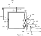
- FIG. 2A shows a superconducting circuit 200a according to at least one implementation, comprising a superconducting resonator 202a with two SQUID loops, able to independently tune the resonator frequency and sensitivity.
- Superconducting resonator 202a comprises two SQUID loops 204a and 204b.
- Each of SQUID loops 204a and 204b is a DC SQUID and comprises a pair of Josephson junctions in parallel with one another to form a superconducting loop.
- SQUID loops 204a and 204b advantageously enable independent tuning of the resonance frequency and the sensitivity of superconducting resonator 202a by adjusting the flux bias in SQUID loops 204a and 204b, as described in PCT Patent Application No. WO2016US31885 (published as International patent application publication WO2016183213A1 ).
- Interfaces 206a and 206b can provide flux bias to SQUID loops 204a and 204b respectively. Once a suitable operating point has been found (see below), the flux biases provided by interfaces 206a and 206b can be static. This advantageously allows superconducting circuit 200a to use an array of flux DACs requiring only a few wires to program. The two tunable SQUID loops 204a and 204b do not need an independent analog control line for each superconducting resonator 202a.
- Superconducting resonator 202a is connected at node 208 to ground, for example to a ground 210 of transmission line 110.
- Superconducting circuit 200a can optionally include an interface 128 operable to apply a flux bias to last shift register stage 114 (also referred to in the present application as a final shift register stage), and can be operated as a superconducting transceiver circuit.
- Last shift register stage 114 can, for example, comprise a QFP, and can be communicatively coupled to superconducting resonator 202a for the purposes of reading out the state of a superconducting device (for example, a superconducting qubit) and/or loading data into the superconducting device.
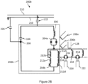
- Figure 2B is a schematic diagram illustrating a second example embodiment of a superconducting circuit 200b comprising a superconducting resonator with two SQUID loops 204a and 204b, able to independently tune the resonator frequency and sensitivity.
- Superconducting resonator 202b comprises two SQUID loops 204a and 204b.
- Each of SQUID loops 204a and 204b is a DC SQUID and comprises a pair of Josephson junctions in parallel in a superconducting loop.
- SQUID loop 204b of Figure 2B further comprises inductances 212a, 212b, 212c, and 212d (collectively referred to as 212).
- SQUID loops 204a and 204b enable independent tuning of the resonance frequency and the sensitivity of superconducting resonator 202b by adjusting the flux bias in SQUID loops 204a and 204b, as described in PCT Patent Application No. WO2016US31885 (published as International patent application publication WO2016183213A1 ).
- SQUID loop 204b is galvanically coupled to a last shift register stage 214 (also referred to in the present application as a final shift register) comprising DC SQUID 216 and inductance 218.
- Interfaces 220 and 222 can provide flux bias to DC SQUIDs 216 and 224 respectively.
- Interfaces 206a and 206b can provide flux bias to SQUID loops 204a and 204b respectively.
- Superconducting resonator 202b is connected at node 208 to ground, for example to a ground 210 of transmission line 110, either directly or via optional coupling capacitor 226.
- Superconducting circuit 200b can optionally include an interface 128 operable to apply a flux bias to last shift register stage 214, and can be operated as a superconducting transceiver circuit.
- Last shift register stage 214 can, for example, comprise a QFP, and can be communicatively coupled to superconducting resonator 202b for the purposes of reading out the state of a superconducting device (for example, a superconducting qubit) and/or loading data into the superconducting device.
- Components of superconducting circuit 200b labeled with the same numbers as in superconducting circuit 100a of Figure 1A and 100b of Figure 1B are similar or even identical to those described in reference to Figures 1A and 1B .
- Components of superconducting circuit 200b labeled with the same numbers as in superconducting circuit 200a of Figure 2A are similar or even identical to those described in reference to Figure 2A .
- Figure 3 shows a readout system 300 for a superconducting circuit 302, according to at least one exemplary implementation.
- superconducting circuit 302 comprises one or more superconducting resonators (not shown in Figure 3 ) such as superconducting resonator 202a of Figure 2A .
- superconducting circuit 302 comprises a superconducting quantum processor.
- superconducting circuit 302 comprises a superconducting classical processor.
- superconducting circuit 302 comprises a superconducting device.
- Readout system 300 comprises a digital board 304 and a microwave board 306.
- Digital board 304 comprises a Field Programmable Gate Array (FPGA) 308, two Digital-to-Analog Converters (DACs) 310a and 310b, and two Analog-to-Digital Converters (ADCs) 312a and 312b.
- digital board 304 comprises two FPGAs, one providing output to DACs 310a and 310b, and the other providing output to ADCs 312a and 312b.
- each of DACs 310a and 310b can include a dual-channel 14-bit DAC operating at up to about 5.6 Gsps (Giga samples per second).
- ADCs 312a and 312b can be implemented using a multi-channel device, for example a quad-channel 10-bit ADC capable of operating in dual-channel mode at up to about 2.5 Gsps.
- Readout system 300 advantageously enables independent addressing of the two side-bands of the Frequency Multiplexed Readout (FMR) spectrum.
- the second term in the argument of the sine function depends on ⁇ and can be used to compensate for the phase imbalance between the two mixer channels that results from the analog nature of the mixer.
- Digital board 304 further comprises two loopback lines 314a and 314b, and a sync/clock connection 316.
- Loopback line 314a connects the output of DAC 310a to the input of ADC 312a.
- Loopback line 314b connects the output of DAC 310b to the input of ADC 312b.
- Microwave subsystem or microwave board 306 further comprises a loopback line 316.
- Loopback line 316 connects the input and output to cryogenic subsystem (not shown in Figure 3 ) used to cool superconducting circuit 302 to temperatures as low as a few mK.
- Loopback lines 314a and 314b on digital board 304, and loopback line 316 on microwave board 306 are optional, and used when required to bypass other elements of readout system 300.
- Readout system 300 further comprises two reconstruction filters 318a and 318b, and two anti-aliasing filters 320a and 320b.
- Reconstruction filters 318a and 318b are low-pass analog filters that can be used to produce a band-limited analog signal from a digital input.
- Anti-aliasing filters 320a and 320b are low-pass analog filters that can be used to band-limit a received signal in order to satisfy or approximately satisfy the sampling theorem over a band of interest.
- Microwave board 306 comprises a Voltage-Controlled Oscillator (VCO)/Phase Locked Loop (PLL) 322 which provides a reference microwave signal, mixers 324 and 326, and programmable attenuators 328.
- Microwave board 306 further comprises amplifiers 330, 332, 334, and 336. Amplifiers 330, 332, 334, and 336 can be used to provide level control on the signal received from superconducting circuit 302.
- Microwave board 306 further comprises a microwave switch 338 controlled by a signal from FPGA 308 on digital board 304.
- mixers 324 and 326 are complex mixers.
- the illustrated readout system 300 further comprises amplifier 340, attenuators 342 and 344, circulators 346 and 348, and DC blocks 350 and 352.
- DC blocks 350 and 352 are used as a thermal break on each of the input and output lines to superconducting circuit 302.
- amplifier 340 and attenuator 342 can operate at 4 K.
- Attenuator 344 can operate at 0.6 K.
- Circulators 346 and 348, and DC blocks 350 and 352, can operate at 8 mK.
- a data rate of approximately 600 Mbps can be achieved for a shift register stage (SRS) operation time of 25 ns.
- SRS shift register stage
- Figure 4 shows a hybrid computing system 400 according to at least one exemplary implementation, including a digital computer 402 and a quantum computer 404, that may incorporate FMR technology as described above.
- Digital computer 402 comprises CPU 406, user interface elements 408, 410, 412, and 414, disk 416, controller 418, bus 420 and memory 422.
- Memory 422 comprises BIOS 424, operating system 426, server modules 428, calculations modules 430, quantum processor modules 432, readout modules 434, and other modules that can be used to operate hybrid computing system 400.
- Quantum computer 404 comprises quantum processor 436, readout control system 438, qubit control system 440 and coupler control system 442.
- Quantum computer 404 can incorporate FMR technology comprising superconducting resonators (such as superconducting resonator 202a of Figure 2A ).
- Computing system 400 can comprise a readout system such as readout system 300 of Figure 3 .
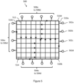
- FIG. 5 shows a first arrangement of superconducting resonators in an example implementation of a superconducting quantum processor 500.
- Processor 500 comprises 64 unit cells (not shown in Figure 5 ) with four sets of superconducting resonators 502a through 502d (collectively superconducting resonators 502), 504a through 504d (collectively superconducting resonators 504), 506a through 506d (collectively superconducting resonators 506), and 508a through 508d (collectively superconducting resonators 508), coupled to outer shift registers 510a through 510d (collectively outer shift registers 510) respectively.
- Processor 500 comprises eight vertically oriented inner shift registers 512 and eight horizontally oriented inner shift registers 514.
- All four sets of superconducting resonators 502, 504, 506, and 508 are coupled to a transmission line, for example line 110 of Figure 2A (not shown in Figure 5 ). In one implementation, all four sets of superconducting resonators 502, 504, 506, and 508 are coupled to a single common transmission line.
- Each arrow in Figure 5 indicates the direction data flows through a respective shift register of inner shift registers 512 and outer shift registers 510 in normal operation.
- FIG. 6 shows a second arrangement of superconducting resonators in an example implementation of a superconducting quantum processor 600.
- Processor 600 comprises 64 qubits (not shown in Figure 6 ) with four sets of superconducting resonators 602a through 602h (collectively superconducting resonators 602), 604a through 604h (collectively superconducting resonators 604), 606a through 606h (collectively superconducting resonators 606), and 608a through 608h (collectively superconducting resonators 608).
- Processor 600 comprises eight vertically oriented inner shift registers 610 and eight horizontally oriented inner shift registers 612.
- Two sets of superconducting resonators 602 and 608 are coupled to a first transmission line such as line 110 of Figure 2A (not shown in Figure 6 ).
- the other two sets of superconducting resonators 604 and 606 are coupled to a second transmission line (also not shown in Figure 6 ).
- outer shift registers (such as outer shift registers 510 of Figure 5 ) are not needed. With eight resonators on a side, one for each of the inner shift registers (horizontal or vertical), there is sufficient fault tolerance provided by the cross-over stages of the horizontally and vertically oriented inner shift registers.
- the present technology can load data into a shift register on a quantum processor chip using a frequency multiplexed resonator.
- the frequency multiplexed resonator readout described above (with reference to Figures 1 , 2A , 2B , 3 , 4 , 5 , and 6 ) can be run in reverse to allow data to be passed to the processor.
- a first stage QFP can be used to rectify a microwave signal in the resonator if a signal is present.
- the present technology can be used to input data to the processor as well as to readout qubit states from the processor.
- the same lines can be used for both input and readout (see, for example, PCT Patent Application No. WO2016US31885 , published as International patent application publication WO2016183213A1 ).
- the frequency multiplexed resonator input system described above which can be used to input data to superconducting devices, is used in combination with the frequency multiplexed resonator readout system also described in the present disclosure (with reference to Figures 1 , 2A , 2B , 3 , 4 , 5 , and 6 ).
- the frequency multiplexed resonator input system described above is used in combination with other readout systems or circuits.
- the frequency multiplexed resonator input system is used in combination with the superconducting flux qubit readout system described in U.S. Patent 8,854,074 "SYSTEMS AND METHODS FOR SUPERCONDUCTING FLUX QUBIT READOUT".
- a return pathway in Figure 3 comprises DC block 350, circulators 348 and 346, amplifiers 340, 336, 334, 332, 330, attenuator 328, mixer 326, filters 320a and 320b, and ADC 312a and 312b. If the system of Figure 3 is to be used for inputting data to the superconducting devices only (and no readout), then the return pathway may be omitted.
- a frequency-multiplexed resonant readout (FMRR) system can use an array of superconducting shunt-coupled resonators strongly coupled to a superconducting transmission line to perform high-speed readout.
- the FMRR system can perform readout of a quantum computer (for example, a quantum annealer).
- one or more resonators of the array of superconducting shunt-coupled resonators strongly coupled to the superconducting transmission line include one or more capacitors.
- the strength of a coupling between a superconducting shunt-coupled resonator and a superconducting transmission line can be increased by using a larger coupling capacitance. Proximity of a capacitor in one of the resonators to the superconducting transmission line can cause a local perturbation of the transmission line impedance, for example in a vicinity of the resonator. In some implementations, a larger capacitance can cause a larger local perturbation of the transmission line impedance.
- a superconducting transmission line can be coupled to a relatively small array of superconducting resonators, each superconducting resonator coupled to the transmission line by a respective coupling capacitance having a relatively large value.
- the total parallel capacitance can cause a deviation from a characteristic impedance of the transmission line (for example a 50 ⁇ impedance).
- a 50 fl impedance is a typical characteristic impedance of a transmission line, and is a typical specification for commercial microwave components.
- a superconducting transmission line can be coupled to a relatively large array of superconducting resonators, each superconducting resonator coupled to the transmission line by a respective coupling capacitance having a relatively small value.
- the total parallel capacitance can cause a deviation from a characteristic impedance of the transmission line (for example. a 50 ⁇ impedance).
- a deviation in the characteristic impedance of the transmission line can depend on a combined parallel capacitance.
- a deviation in the characteristic impedance of the transmission line can depend on a combined loading of more than one resonator.
- the resonators can be neighboring resonators.
- a deviation in the characteristic impedance of the transmission line can depend on other factors.
- a deviation from a design impedance over the length of the resonator array can cause ripple or ripples, and can change the strength of coupling between the resonator and the superconducting transmission line. In some instances, the strength of coupling can be changed from a design value or a desired value.
- a change to the impedance of the transmission line caused by the presence of stray capacitance C' can, in turn, affect the strength of coupling of one or more resonators to the transmission line.
- the strength of coupling can be characterized, for example, by an external quality factor Q EXT , defined such that a lower value of Q EXT corresponds to a stronger coupling between the resonator and the transmission line.
- Q EXT external quality factor
- the impact of an impedance change on the strength of the coupling between a resonator and a transmission line can depend on the type of coupling.
- the external quality factor can be expressed at least approximately as follows: Q EXT ⁇ 2 Z 0 ⁇ L R ⁇ ⁇ 0 3 ⁇ C C 2 where L R is the inductance of the resonator, ⁇ 0 is the resonant frequency of the resonator, and C c is the capacitance of a coupling capacitor between the resonator and the transmission line.
- a weaker coupling can cause a weaker resonance.
- the depth of a resonance was reduced by more than 4dB when the value of Q EXT was doubled.
- One approach for mitigating the effect of an impedance change on the strength of coupling is to drive each resonator at a power individually selected to compensate for its modified coupling to the transmission line.
- a shortcoming of this approach can be that it may be necessary to provide an in-situ calibration of each resonator's coupling to the transmission line, by sweeping through power levels, and looking for an onset of resonator nonlinearity.
- An in-situ calibration can be time-consuming, and it may be necessary for the system to include a generator with a wider dynamic range.
- Q EXT can vary along the length of a transmission line, and can depend on a number of factors including the number of superconducting resonators coupled to the transmission line, the values of the coupling capacitances, and the spacing between superconducting resonators.
- Another approach for mitigating the effect of an impedance change on the strength of coupling is to spread out the additional coupling capacitance along the transmission line to minimize, or at least reduce, the additional coupling capacitance per unit length.
- One example implementation is to use ⁇ /4 distributed-element resonators capacitively coupled to the transmission line over a distance of a few hundred microns.
- distributed-element coupling can be implemented using a high-quality silicon substrate for a capacitor dielectric.
- distributed-element coupling can be lossy.
- a distributed readout resonator design can have a larger footprint than a lumped-element design.
- a distributed-element design can have a footprint of approximately 400 ⁇ 600 ⁇ m 2
- a lumped-element design can have a footprint of approximately 100 ⁇ 100 ⁇ m 2 .
- a desire for a smaller footprint can drive a lumped-element implementation of shunt-coupled resonators strongly-coupled to a transmission in a multi-layer stack.
- An interaction between a transmission line and a resonator, as described above, can be more important for more strongly-coupled resonators. While weaker coupling allows more resonators to be packed into a given bandwidth, and weaker coupling may be sufficient for slower readout times, commercial applications where readout speed is important (such as commercial quantum computing applications) may advantageously employ stronger coupling.
- a data rate of N weakly-coupled resonators, each with linewidth W can be at least similar to a data rate of a strongly-coupled resonator with line width N ⁇ W.
- the N weakly-coupled resonators may advantageously spatially distribute a perturbation to the transmission line.
- Coupling strength may advantageously be selected based at least in part on topological considerations and/or to at least attempt to match clock domains. For example, it can be advantageous to end each shift register with a detector which makes the number of resonators equal to twice the sum of the number of rows and the number of columns.
- Figure 5 illustrates an example topology.
- the coupling of a resonator to a transmission depends at least in part on the linewidth of a resonator.
- the linewidth can be determined by dividing the available bandwidth by the linewidth and by an additional factor selected to provide enough room between resonances in the frequency domain.
- the available bandwidth is 2.5 GHz.
- the additional factor is 4.
- a shift register can operate at a speed set by driving electronics. It can be advantageous for the detectors to match or exceed the speed set by the driving electronics. If, for example, the detector is faster than the shift register, it can be an inefficient use of available bandwidth.
- a shift register delivers data every 100 ns, and resonances are copuled to provide a response time of 20 ns. Coupling them twice as strongly may reduce a full duty cycle time from 120 ns to 110 ns. The reduction in full duty cycle time is only a marginal improvement yet requires twice the FMRR bandwidth. At least for this reason, it can be advantageous for the detector to match the shift register speed.
- proximity of resonators to a superconducting transmission line can cause an undesirable level of ripple when measured in transmission, and can have an undesirable variation in the coupling strength of resonators as a function of the position of the resonators along the transmission line.
- the impact can include a limit on the number of usable resonators in a frequency-multiplexed resonant readout system, with a concomitant slowdown in readout speed and less redundancy.
- Distributed-element approaches typically rely on a single metal-layer fabrication stack and use a large footprint.
- the systems and methods described in the present application support a smaller, and more flexible footprint, and a multi-layer fab stack.
- at least one inductance is introduced into the center line of the transmission line.
- the inductance can modify a characteristic impedance of the transmission line.
- the impedance is selected to at least partially compensate for variations in the impedance of the transmission line, for example to at least partially compensate for local variations in the impedance of the transmission line caused by proximity of a capacitance in a microwave superconducting resonator coupled to the transmission line.
- lumped-element inductors are introduced into the center line of the transmission line, at least one on each side of each resonator. At least one lumped-element inductor is introduced into the center line of the transmission line upstream of the resonator, and at least one lumped-element inductor is introduced into the center line of the transmission line downstream of the resonator. Each lumped-element inductor can be selected to compensate for a local change in impedance caused by a respective coupled resonator.
- a configuration of one or more inductances added to the transmission line can depend on a position of the resonator along the transmission line and a spacing of resonators in an array of superconducting resonators.
- a value of the one or more inductances can be selected to compensate for a local perturbation to the characteristic impedance of the transmission line.
- the arrangement of inductances can be symmetric or asymmetric.
- the configuration of inductances can vary from one superconducting resonator in the array of superconducting resonances to another.
- a compensating inductance for a superconducting resonator can vary with a position of the superconducting resonator along the length of the transmission line e.g. whether the superconducting resonator is close to one end of the transmission line or near the middle of the transmission line.
- a symmetric configuration of a pair of inductances may provide a preferred level of compensation in the middle of a transmission line
- an asymmetric configuration of inductances may provide a preferred level of compensation near an end of the transmission line.
- Any suitable method can be used to estimate the preferred values and arrangement of compensating inductances for an array of superconducting resonators.
- a first-order analysis may be sufficient for practical purposes in some applications.
- the value of a compensating inductance can be estimated by any suitable method including, but not limited to, the methods described below.
- an iterative method can be used to estimate the value of compensating inductances for an array of superconducting resonators.
- the iterative method can at least partially take into account an interdependency between compensating inductances.
- the iterative method can include iteratively adjusting the value of a compensating inductance of a set of compensating inductances so that, for other compensating inductances in the set of compensating inductances, the transmission line appears to have an impedance of 50 ⁇ .
- L comp Z 0 2 C eff
- Z 0 is a characteristic impedance of the transmission line
- C eff is an effective capacitance of the shunt-coupled resonator
- the effect of a coupling capacitor coupling a superconducting resonator to the transmission line can be a local perturbation of the impedance of the transmission line.
- one or more compensating inductances are introduced into the transmission line in proximity to the superconducting resonator.
- one or more compensating inductances are introduced in other suitable configurations, for example further away from the superconducting resonator.
- FIG. 7A is a schematic circuit diagram illustrating a first example superconducting circuit 700a of a shunt-coupled resonator according to the present disclosure.
- Superconducting circuit 700a includes a superconducting resonator 202a (comprising elements encompassed by a broken-line box in Figure 7A ).
- Superconducting resonator 202a comprises two SQUID loops 204a and 204b able to independently tune a frequency and a sensitivity of superconducting resonator 202a.
- Each of SQUID loops 204a and 204b is a DC SQUID that comprises a pair of Josephson junctions (represented by crosses in Figure 7A ) in parallel with one another to form a superconducting loop.
- SQUID loops 204a and 204b advantageously enable independent tuning of the resonance frequency and the sensitivity of superconducting resonator 202a by adjusting the flux bias in SQUID loops 204a and
- superconducting circuit 700a labeled with the same numbers as in superconducting circuit 100a, 100b of Figures 1A and 1B , respectively, and/or superconducting circuit 200a of Figure 2A are similar, or even identical, to those described in reference to Figures 1A , 1B and 2A , respectively.
- Superconducting resonator 202a includes a capacitance 104 and an inductance 106. Interfaces 206a and 206b can provide flux bias to SQUID loops 204a and 204b respectively. Superconducting resonator 202a is connected at node 208 to ground, for example to a ground 210 of transmission line 110.
- Superconducting circuit 700a can optionally include an interface 128 operable to apply a flux bias to last shift register stage 114 (also referred to in the present application as final shift register stage 114).
- Interface 128 can be operated as a superconducting transceiver circuit.
- Last shift register stage 114 (comprising elements encompassed by a broken-line box in Figure 7A ) can, for example, comprise a QFP.
- Last shift register stage 114 can be communicatively coupled to superconducting resonator 202a for the purposes of reading out the state of a superconducting device and/or loading data into a superconducting device.
- Superconducting circuit 700a includes inductances 702a and 702b.
- Inductance 702a can include a lumped-element magnetic inductance, a distributed magnetic inductance, a lumped-element kinetic inductance and/or a distributed kinetic inductance.
- Inductance 702b can include a lumped-element magnetic inductance, a distributed magnetic inductance, a lumped-element kinetic inductance and/or a distributed kinetic inductance.
- each of inductances 702a and 702b includes a respective lumped-element inductance. In another implementation, at least one of inductances 702a and 702b includes a distributed-element inductance. In yet another implementation, at least one of inductances 702a and 702b includes a kinetic inductance.
- Inductance 702a is on one side of the transmission line relative to superconducting resonator 202a, and inductance 702b is on the other side of the transmission line relative to superconducting resonator 202a.
- inductance 702a is upstream of superconducting resonator 202a, and inductance 702b is downstream of superconducting resonator 202a, with respect to a direction of signal flow.
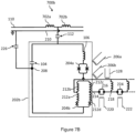
- Figure 7B is a schematic circuit diagram illustrating a second example superconducting circuit 700b of a shunt-coupled resonator according to the present disclosure.
- Superconducting circuit 700b includes a superconducting resonator 202b (comprising elements encompassed by a broken-line box in Figure 7B ) that includes two SQUID loops 204a and 204b.
- Each of SQUID loops 204a and 204b is a DC SQUID that comprises a pair of Josephson junctions (represented by crosses) in parallel to form a superconducting loop.
- SQUID loop 204b of Figure 7B further comprises inductances 212a, 212b, 212c, and 212d.
- SQUID loops 204a and 204b can enable independent tuning of a resonance frequency and a sensitivity of superconducting resonator 202b. Tuning can include adjusting a flux bias in SQUID loops 204a and 204b.
- SQUID loop 204b is galvanically coupled to a last shift register stage 214 comprising DC SQUID 216 and inductance 218. Interfaces 220 and 222 can provide flux bias to DC SQUIDs 216 and 224 respectively.
- Interfaces 206a and 206b can provide flux bias to SQUID loops 204a and 204b respectively.
- Superconducting resonator 202b is connected at node 208 to ground, for example to the ground 210 of transmission line 110, either directly or via optional coupling capacitor 226.
- Superconducting circuit 700b can optionally include an interface 128 operable to apply a flux bias to last shift register stage 214.
- interface 128 can be operated as a superconducting transceiver circuit.
- Last shift register stage 214 can, for example, comprise a QFP, and can be communicatively coupled to superconducting resonator 202b for the purposes of reading out the state of a superconducting device and/or loading data into a superconducting device.
- Components of superconducting circuit 700b labeled with the same numbers as in superconducting circuit 100a of Figure 1A and 100b of Figure 1B are similar or even identical to those described in reference to Figures 1A and 1B .
- Components of superconducting circuit 700b labeled with the same numbers as in superconducting circuit 200a of Figure 2A are similar or even identical to those described in reference to Figure 2A .
- Superconducting circuit 700b includes inductances 702a and 702b.
- inductances 702a and 702b are lumped-element inductances.
- at least one of inductances 702a and 702b includes a distributed-element inductance.
- at least one of inductances 702a and 702b includes a kinetic inductance.
- Circuits 700a and 700b each include coupling capacitance 112 (also referred to in the present application as coupling capacitance C C ) and shunt capacitance 104 (also referred to in the present application as shunt capacitance C S ).
- Effective capacitance C eff can be approximately equal to coupling capacitance C C ( C eff ⁇ C C ) when coupling capacitance C C is much less than shunt capacitance C S ( C C ⁇ C S ).
- a kinetic inductance can be introduced into the center line of the transmission line.
- the kinetic inductance can be provided by a kinetic inductor.
- Each kinetic inductor can be placed in-line with the center pin of the transmission line close to a respective resonator.
- a kinetic inductor of a given thickness and material for providing a suitable compensating inductance can be estimated or can be determined empirically.
- a kinetic inductor is fabricated using titanium nitride (TiN), where the thickness of the kinetic inductor is 50 nm, inductance per square L s is 15 pH, compensating inductance L comp is 40 pH, and length l is 1.3 ⁇ m.
- a kinetic inductor is fabricated using titanium nitride (TiN), where the thickness of the kinetic inductor is 50 nm, inductance per square L s is 15 pH, compensating inductance L comp is 120 pH, and length l is 4.0 ⁇ m.
- TiN titanium nitride
- a kinetic inductor is fabricated using niobium nitride (NbN), where the thickness of the kinetic inductor is 35 nm, inductance per square L s is 7 pH, compensating inductance L comp is 40 pH, and length l is 2.9 ⁇ m.
- a kinetic inductor is fabricated using niobium nitride (NbN), the thickness of the kinetic inductor is 50 nm, inductance per square L s is 7 pH, compensating inductance L comp is 120 pH, and length l is 8.6 ⁇ m.
- the line width of the kinetic inductor is 0.5 ⁇ m.
- a superconducting transmission line is a coaxial transmission line.
- a superconducting transmission line is a co-planar waveguide.
- Lumped-element magnetic inductances and/or kinetic inductances can be placed near one or more resonators of an array of superconducting resonators in accordance with the present disclosure to compensate for local changes to impedance of a coaxial transmission line and/or a co-planar transmission line.
- lumped-element inductors also referred to in the present application as lumped-element magnetic inductances
- kinetic inductors also referred to in the present application as lumped-element kinetic inductances
- the capacitance in the superconducting resonator (for example, capacitance 104 in resonator 202a of Figure 7A ) has a high-quality factor (Q).
- the capacitance in the superconducting resonator is a superconducting parallel plate capacitor with a thin, high-permittivity dielectric.
- a parallel-plate design with a thin dielectric can reduce the volume of dielectric for a given capacitance value. Reducing the volume of lossy dielectric can lead to a decrease in the required power to saturate a superconducting resonator such as superconducting resonator 202a of Figure 7A . It can also provide a reduced capacitor footprint which is an advantage where chip space is at a premium.
- a superconducting parallel plate thin-layer capacitor is integrated in a heterogeneous multi-layer planarized fabrication stack with deposited dielectrics.
- a method for fabricating a thin-layer capacitor suitable for use in a superconducting resonator is described in PCT Patent Application No. WO2016US31885 (published as International patent application publication WO2016183213A1 ) "FREQUENCY MULTIPLEXED RESONATOR INPUT AND/OR OUTPUT FOR A SUPERCONDUCTING DEVICE".
- a superconducting resonator can be inductively coupled to the superconducting transmission line.
- Figure 8A is a schematic circuit diagram illustrating a non-claimed example superconducting circuit 800a of an inductively-coupled resonator.
- Superconducting circuit 800a includes a superconducting resonator 202a (comprising elements encompassed by a broken-line box in Figure 8A ) that includes two SQUID loops 204a and 204b.
- Each of SQUID loops 204a and 204b is a DC SQUID that comprises a pair of Josephson junctions (represented by crosses in Figure 8A ) in parallel to form a superconducting loop.
- SQUID loops 204a and 204b advantageously enable independent tuning of a resonance frequency and a sensitivity of superconducting resonator 202a by adjusting a flux bias in SQUID loops 204a and 204b.
- SQUID loop 204b is inductively coupled to a last shift register stage 114. Interfaces 206a and 206b can provide flux bias to SQUID loops 204a and 204b respectively.
- Superconducting circuit 800a can optionally include an interface 128 operable to apply a flux bias to last shift register stage 114, and can be operated as a superconducting transceiver circuit.
- Last shift register stage 114 can, for example, comprise a QFP, and can be communicatively coupled to superconducting resonator 202a for the purposes of reading out the state of a superconducting device and/or loading data into a superconducting device.
- Components of superconducting circuit 800a labeled with the same numbers as in superconducting circuit 100a of Figure 1A and 100b of Figure 1B are similar or even identical to those described in reference to Figure 1 .
- Components of superconducting circuit 800a labeled with the same numbers as in superconducting circuit 200a of Figure 2A are similar or even identical to those described in reference to Figure 2A .
- Superconducting resonator 202a includes inductance 802.
- the value of inductance 802 is approximately the same as the value of inductance 106.
- Superconducting circuit 800a includes inductances 804a and 804b to inductively couple superconducting resonator 202a to superconducting transmission line 110.
- Superconducting circuit 800a includes capacitors 806a and 806b. Capacitors 806a and 806b can compensate for a local change in the impedance of superconducting transmission line 110. In some implementations, the local change in the impedance is a deviation from 50 ⁇ .
- compensating capacitances 806a and 806b are arranged at least approximately symmetrically either side of the inductive coupling in proximity to the inductive coupling. In other implementations, one or more compensating capacitances can be used in a suitable arrangement. Variations in the arrangement can include the number of capacitances, and their placement and spacing with respect to each other and the superconducting resonator.
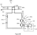
- Figure 8B is a schematic circuit diagram illustrating a second non-claimed example of a superconducting circuit 800b of an inductively-coupled resonator.
- Superconducting resonator 202a of Figure 8B is inductively coupled to superconducting transmission line 110 via inductance 810.
- Superconducting resonator 202a can be galvanically coupled to the inductance.
- inductance 810 is a kinetic inductance.
- Capacitors 806a and 806b can be selected and arranged to compensate for a local perturbation to the characteristic impedance of superconducting transmission line 110. In some implementations, capacitors 806a and 806b are selected and arranged to maintain the characteristic impedance of superconducting transmission line 110 at 50 ⁇ .
- each of superconducting circuits 100, 200a, 200b, 700a, 700a, 700b, 800a, and 800b of Figures 1 , 2A , 2B , 7A , 7B , 8A , and 8B , respectively, is based at least in part on the use of flux-tunable inductances included in their respective superconducting resonators 202a and 202b.
- a flux-tunable inductance can be realized using a DC-SQUID that includes two Josephson Junctions fabricated with a tunnel barrier process.
- a flux-tunable inductance realized using a DC-SQUID is illustrated in each of superconducting circuits 100a, 100b, 200a, 200b, 700a, 700a, 700b, 800a, and 800b of Figures 1A , 1B , 2A , 2B , 7A , 7B , 8A , and 8B , respectively.
- a tunable inductance can be realized using an RF-SQUID that includes a single Josephson junction in parallel with an inductance.
- a flux-tunable inductance can be realized using an RF-SQUID or a DC- SQUID where the RF-SQUID or DC-SQUID is formed using a combination of one or more inductances selected from a list that includes kinetic inductance, magnetic inductance, tunnel barrier Josephson Junctions, or weak-link Josephson Junctions.
Landscapes
- Engineering & Computer Science (AREA)
- Physics & Mathematics (AREA)
- Theoretical Computer Science (AREA)
- General Physics & Mathematics (AREA)
- Mathematical Physics (AREA)
- Data Mining & Analysis (AREA)
- Software Systems (AREA)
- Condensed Matter Physics & Semiconductors (AREA)
- Mathematical Analysis (AREA)
- Mathematical Optimization (AREA)
- Pure & Applied Mathematics (AREA)
- Computing Systems (AREA)
- General Engineering & Computer Science (AREA)
- Computational Mathematics (AREA)
- Evolutionary Computation (AREA)
- Artificial Intelligence (AREA)
- Electromagnetism (AREA)
- Chemical & Material Sciences (AREA)
- Nanotechnology (AREA)
- Crystallography & Structural Chemistry (AREA)
- Superconductor Devices And Manufacturing Methods Thereof (AREA)
- Logic Circuits (AREA)
- Control Of Motors That Do Not Use Commutators (AREA)
Description
- This disclosure generally relates to input and/or output systems and methods for superconducting devices such as superconducting quantum computers and superconducting classical computers, and, more specifically, to systems and methods for inputting data to a superconducting quantum processor and/or measuring the state of a qubit in the superconducting quantum processor.
- Superconducting microwave resonators have been used in a variety of fields including, but not limited to, quantum computation and astronomy. For example, in quantum computation, superconducting resonators have been used to detect the state of qubits. In astronomy, superconducting microwave resonators have been used in Microwave Kinetic Inductance Detectors (MKIDs). In both cases, many resonators (used as detectors or in detectors) can be coupled to a common transmission line and integrated through frequency domain multiplexing. Frequency domain multiplexing (FDM) is a technique in which a communication bandwidth is divided into a number of non-overlapping sub-bands, each sub-band used to carry a separate signal.
- Using FMR technology, superconducting resonators of different resonant frequencies can be used for readout of multiple qubits. The resonators can share a common microwave transmission line by using frequency domain multiplexing.
- "A frequency and sensitivity tunable microresonator array for high-speed quantum processor readout", Journal of applied physics, American institute of Physics, US Vol. 119, no. 1, discloses a microresonator array for high-speed quantum processor readout.
US 2016/0125309 A1 discloses quantum systems including a qubit and a transmission line resonator having an associated resonant wave-length.2009/0289638 A1 discloses a method for determining whether a quantum system comprising a superconducting qubit is occupying a first basis state or a second basis state once a measurement is performed.US 5,153,171 discloses a superconducting variable phase shifter providing improved performance in the microwave and millimeter wave frequency ranges.US 2005/0184284 A1 discloses a method of coupling a qubit. - Frequency Multiplexed Resonator (FMR) technology can be used to readout many single flux quanta simultaneously, and it has applications in both superconducting quantum computing and superconducting classical computing. FMR technology can also have applications in inputting data to a superconducting quantum processor, for example via a Quantum Flux Parametron (QFP) device. FMR technology can, for example, provide a scalable input/output technology.
- The systems and methods described in the present application relate to aspects of FMR technology including a) the use an array of superconducting shunt-coupled resonators strongly coupled to a superconducting transmission line to perform high-speed readout, and b) approaches to at least partially compensate for transmission line impedance variations that can occur in the vicinity of the superconducting shunt-coupled resonators.
- A superconducting circuit is defined according to the claims.
- In the drawings, identical reference numbers identify similar elements or acts. The sizes and relative positions of elements in the drawings are not necessarily drawn to scale. For example, the shapes of various elements and angles are not necessarily drawn to scale, and some of these elements are arbitrarily enlarged and positioned to improve drawing legibility. Further, the particular shapes of the elements as drawn, are not necessarily intended to convey any information regarding the actual shape of the particular elements, and have been solely selected for ease of recognition in the drawings.
-
Figure 1A is a schematic diagram illustrating an example embodiment of a superconducting circuit comprising a superconducting resonator able to tune a resonator frequency. -
Figure 1B is a schematic diagram illustrating an example embodiment of a superconducting circuit comprising a superconducting resonator able to tune a resonator frequency. -
Figure 2A is a schematic diagram illustrating a first example embodiment of a superconducting circuit comprising a superconducting resonator with two SQUID loops, able to independently tune the resonator frequency and sensitivity. -
Figure 2B is a schematic diagram illustrating a second example embodiment of a superconducting circuit comprising a superconducting resonator with two SQUID loops, able to independently tune the resonator frequency and sensitivity. -
Figure 3 is a schematic diagram illustrating an example embodiment of a readout system for a superconducting circuit. -
Figure 4 is a schematic diagram of an exemplary hybrid computing system, including a digital computer and a quantum computer, that may incorporate FMR technology as described herein. -
Figure 5 is a schematic diagram illustrating a first arrangement of superconducting resonators in an example embodiment of a superconducting quantum processor. -
Figure 6 is a schematic diagram illustrating a second arrangement of superconducting resonators in an example embodiment of a superconducting quantum processor. -
Figure 7A is a schematic circuit diagram illustrating a first example superconducting circuit of a shunt-coupled resonator according to the present disclosure. -
Figure 7B is a schematic circuit diagram illustrating a second example superconducting circuit of a shunt-coupled resonator according to the present disclosure. -
Figure 8A is a schematic circuit diagram illustrating a non-claimed superconducting circuit of an inductively-coupled resonator. -
Figure 8B is a schematic circuit diagram illustrating a second non-claimed superconducting circuit of an inductively-coupled resonator. - Qubit: A qubit (also referred to in the present application as a quantum bit) is a basic unit of quantum information, and is a quantum version of a classical binary bit that can be physically realized with a two-state device. A qubit is a two-state quantum-mechanical system. A qubit also refers to the actual physical device in which information is stored. For example, superconducting qubits are a type of superconducting device that can be included in a superconducting integrated circuit. Superconducting qubits can, for example, take the form of charged based or flux based qubits.
- Superconducting device: A superconducting device is an electronic device that makes use of the properties of a superconducting material, for example zero electrical resistance and expulsion of magnetic flux when cooled below a critical temperature characteristic of the superconducting material.
- Microwave transmission line: A microwave transmission line is a cable or other structure that includes one or more conductors operable to carry alternating electrical current of microwave frequency.
- SQUID (Superconducting Quantum Interference Device): A SQUID is a superconducting device that includes a superconducting loop containing one or more Josephson junctions. A SQUID can be used as a magnetometer able to measure very low magnetic fields. A DC SQUID has two Josephson junctions connected in parallel. An rf-SQUID has a superconducting loop containing a single Josephson junction.
- Lumped Element Design: In a lumped element design, a spatially distributed physical system is described as a topology of discrete entities that approximate the behavior of the distributed system under certain assumptions. It is useful in electrical and electronic systems, for example.
- Shift Register: A shift register is a sequential logic circuit operable to store and/or transfer data.
- Quantum Flux Parametron (QFP): A QFP is a logic circuit that includes at least one superconducting Josephson junction and a resonant circuit in which an oscillation can be made to represent a binary digit. Though its design makes use of quantum principles, a QFP is an element of classical computing technology rather than quantum computing technology.
- Hybrid Computer: A hybrid computer is a system that includes at least one digital processor, and at least one analog processor (e.g. a quantum processor).
- Ripple: Ripple is an at least approximately periodic variation in signal. On a transmission line, for example, ripple can be caused by an impedance mismatch that leads to generation of a standing wave.
- Josephson Junction: A Josephson junction is device that includes two electrodes of material that can superconduct at or below a critical temperature characteristic of the material, and a thin insulating barrier separating the electrodes.
- Weak-Link Josephson Junction: A weak-link Josephson junction is a type of Josephson junction in which a metallic constriction with dimensions of the order of the superconducting coherence length bridges two superconducting electrodes. A weak-link Josephson junction can behave as an inductance.
- Flux Digital-to-Analog Converter (DAC): A flux DAC is a superconducting device in which magnetic flux quantum representations of digital signals can be established, converted into analog supercurrents, and administered to another device, e.g. a programmable device.
- In the following description, some specific details are included to provide a thorough understanding of various disclosed embodiments. One skilled in the relevant art, however, will recognize that embodiments may be practiced without one or more of these specific details, or with other methods, components, materials, etc. In other instances, well-known structures associated with superconductive circuits or resonators have not been shown or described in detail to avoid unnecessarily obscuring descriptions of the embodiments of the present methods. Throughout this specification and the appended claims, the words "element" and "elements" are used to encompass, but are not limited to, all such structures, systems, and devices associated with superconductive circuits and resonators.
- Unless the context requires otherwise, throughout the specification and claims which follow, the word "comprise" is synonymous with "including," and is inclusive or open-ended (i.e., does not exclude additional, unrecited elements or acts).
- Reference throughout this specification to "one embodiment" "an embodiment", "another embodiment", "one example", "an example", "another example", "one implementation", "another implementation", or the like means that a particular referent feature, structure, or characteristic described in connection with the embodiment, example, or implementation is included in at least one embodiment, example, or implementation. Thus, the appearances of the phrases "in one embodiment", "in an embodiment", "another embodiment" or the like in various places throughout this specification are not necessarily all referring to the same embodiment, example, or implementation. Furthermore, the particular features, structures, or characteristics may be combined in any suitable manner in one or more embodiments, examples, or implementations.
- It should be noted that, as used in this specification and the appended claims, the singular forms "a," "an," and "the" include plural referents unless the content clearly dictates otherwise. Thus, for example, reference to a readout system including "a superconducting resonator" includes a single superconducting resonator, or two or more superconducting resonators. It should also be noted that the term "or" is generally employed in its sense including "and/or" unless the content clearly dictates otherwise.
- The headings provided herein are for convenience only and do not interpret the scope or meaning of the embodiments.
-
Figure 1A shows a superconducting circuit 100a comprising asuperconducting resonator 102 according to at least a first exemplary implementation.Superconducting resonator 102 comprises acapacitance 104, and aninductance 106, which may or may not take the form of discrete capacitors and inductors, respectively. -
Superconducting resonator 102 further comprises asingle SQUID loop 108.SQUID loop 108 is a DC SQUID and comprises a pair of Josephson junctions 108-1 and 108-2 in parallel with one another to form a superconducting loop.SQUID loop 108 enables tuning of a resonance frequency ofsuperconducting resonator 102 by adjusting a SQUID flux bias. - A resonance frequency ω of
superconducting resonator 102 can be determined by the following relationship for an LC circuit:
capacitance 104 and L is the sum ofgeometric inductance 106 and the parallel sum of Josephson inductances from Josephson junctions 108-1 and 108-2 inSQUID loop 108. - Small fluctuations in capacitance C and/or inductance L can result in a fractional frequency perturbation of the resonance frequency as follows:

- In one implementation,
superconducting resonator 102 is a distributed resonator. In other implementations,superconducting resonator 102 is a lumped element design. A lumped element design can advantageously provide a bandwidth greater than one octave, and can reduce or minimize the extent of the electric field ofsuperconducting resonator 102. Since a loss tangent ofsuperconducting resonator 102 can depend on a volume of lossy dielectric exposed to the electric field ofsuperconducting resonator 102, it can be beneficial to use a lumped element design. - In a lumped element design,
capacitance 104 can be implemented using one or more capacitors. The capacitors can be interdigitated capacitors and/or parallel plate capacitors. In one implementation,capacitance 104 is implemented using a parallel plate capacitor. In one example, the capacitance of the parallel plate capacitor is approximately 2 pF. - In a lumped element design,
inductance 106 can be implemented using one or more inductors. In one implementation,inductance 106 is implemented using a niobium spiral inductor. In one example, the geometric inductance of the spiral inductor is approximately 1 nH. In another implementation,inductance 106 is implemented using a spiral inductor comprising a high kinetic inductance material, for example titanium nitride (TiN) or tungsten silicide (WSi). - Energy can be stored in the kinetic energy of charge carriers in a conductor driven at AC frequencies, and the stored kinetic energy can be associated with a kinetic inductance of the conductor. The total inductance can be a sum of a geometric inductance and the kinetic inductance. The kinetic inductance can be negligible in a normal (non-superconducting) metal. The kinetic inductance of a superconductor (such as TiN or WSi) can make a significant contribution to the total inductance.
- Energy stored in the inertia of superconducting pairs can contribute a kinetic inductance. The total inductance in
superconducting resonator 102 can be a sum of the geometric inductance, the kinetic inductance, and the inductance ofSQUID loop 108. - Circuit 100a further comprises a
transmission line 110, acoupling capacitance 112, and a last shift register stage 114 (also referred to in the present application as a final shift register stage). Lastshift register stage 114 comprisesinductances SQUID loop 120 andinterface 122. Lastshift register stage 114 may, for example, take the form of a Quantum Flux Parametron (QFP). Lastshift register stage 114 is the endpoint of a shift register comprising one or more stages. Lastshift register stage 114 is a stage that can be communicatively coupled tosuperconducting resonator 102 for the purposes of reading out the state of a superconducting device. In one implementation,superconducting resonator 102 is communicatively coupled to a flux shift register which, in turn, is communicatively coupled to a flux qubit. - The quantum flux parametron (QFP) is a superconducting Josephson junction device similar in structure to a shunted DC SQUID. In the present application, the term "quantum flux parametron" can refer to both the operation and the structure of the superconducting Josephson junction device.
-
Interface 124 can provide a flux bias toSQUID loop 108 and can be controlled by a flux digital-to-analog converter (DAC) (not shown inFigure 1 ) or by an analog line, for example. Using a flux DAC can reduce the number of low-frequency analog control lines to superconducting circuit 100a. In the present application, a flux DAC is a specialized superconducting device, and is different, for example, from DACs 310a and 310b ofFigure 3 inreadout system 300. A more detailed description of a flux DAC can be found, for example, inU.S. Patent 8,786,476 SYSTEMS, METHODS AND APPARATUS FOR DIGITAL-TO-ANALOG CONVERSION OF SUPERCONDUCTING MAGNETIC FLUX SIGNALS. -
Superconducting resonator 102 can be coupled totransmission line 110 viacoupling capacitance 112. In one implementation,capacitance 112 includes a discrete capacitor.Transmission line 110 can optionally be coupled to one or more other superconducting resonators (not shown inFigure 1 ). The one or more other superconducting resonators may belong to an array of superconducting resonators. -
Superconducting resonator 102 is connected atnode 126 to ground. - Superconducting circuit 100a can optionally include an
interface 128 operable to apply a flux bias to lastshift register stage 114, and superconducting circuit 100a can be operated as a superconducting transceiver circuit. Lastshift register stage 114 can, for example, comprise a QFP, and can be communicatively coupled tosuperconducting resonator 102 for the purposes of reading out the state of a superconducting device (for example, a superconducting qubit) and/or loading data into the superconducting device. -
Superconducting resonator 102 comprisingsingle SQUID loop 108 does not enable independent tuning of the resonance frequency and the sensitivity ofsuperconducting resonator 102. It can be desirable to have a superconducting resonator in which resonator frequency and sensitivity can be independently adjusted to provide a suitable operating point. For example, independent adjustment of resonant frequency and sensitivity can be used to compensate for frequency shifts arising from variations occurring during fabrication of superconducting circuits such as superconducting circuit 100a ofFigure 1 . -
Figure 1B shows a superconducting circuit 100b comprising asuperconducting resonator 102 and atunable coupler 130 according to at least a first exemplary implementation. Superconducting circuit 100b is similar in at least respects to superconducting circuit 100a, and similar or even identical structures are identified inFigure 1B using the same reference numbers as used inFigure 1A . Only some of the significant differences are described below. - Superconducting circuit 100b includes a
tunable coupler 130 to provide inductive communicative coupling betweenDC SQUID 108 and lastshift register stage 114. Withtunable coupler 130, superconducting circuit 100b can enable independent tuning of the resonance frequency and the sensitivity to QFP flux, provided the variable loading ofsuperconducting resonator 102 by the tunable coupler is taken into account. In one implementation,tunable coupler 130 includes twoinductances DC SQUID 136, and interfaces 138 and 140. -
Figure 2A shows asuperconducting circuit 200a according to at least one implementation, comprising asuperconducting resonator 202a with two SQUID loops, able to independently tune the resonator frequency and sensitivity.Superconducting resonator 202a comprises twoSQUID loops SQUID loops SQUID loops superconducting resonator 202a by adjusting the flux bias inSQUID loops PCT Patent Application No. WO2016US31885 WO2016183213A1 ). - Components of
superconducting circuit 200a labeled with the same numbers as in superconducting circuit 100a, 100b ofFigures 1A and1B are similar, or even identical, to those described in reference toFigures 1A and1B . -
Interfaces SQUID loops interfaces superconducting circuit 200a to use an array of flux DACs requiring only a few wires to program. The twotunable SQUID loops superconducting resonator 202a. -
Superconducting resonator 202a is connected atnode 208 to ground, for example to aground 210 oftransmission line 110. -
Superconducting circuit 200a can optionally include aninterface 128 operable to apply a flux bias to last shift register stage 114 (also referred to in the present application as a final shift register stage), and can be operated as a superconducting transceiver circuit. Lastshift register stage 114 can, for example, comprise a QFP, and can be communicatively coupled tosuperconducting resonator 202a for the purposes of reading out the state of a superconducting device (for example, a superconducting qubit) and/or loading data into the superconducting device. -
Figure 2B is a schematic diagram illustrating a second example embodiment of asuperconducting circuit 200b comprising a superconducting resonator with twoSQUID loops -
Superconducting resonator 202b comprises twoSQUID loops SQUID loops SQUID loop 204b ofFigure 2B further comprisesinductances -
SQUID loops superconducting resonator 202b by adjusting the flux bias inSQUID loops PCT Patent Application No. WO2016US31885 WO2016183213A1 ). -
SQUID loop 204b is galvanically coupled to a last shift register stage 214 (also referred to in the present application as a final shift register) comprisingDC SQUID 216 andinductance 218.Interfaces DC SQUIDs -
Interfaces SQUID loops Superconducting resonator 202b is connected atnode 208 to ground, for example to aground 210 oftransmission line 110, either directly or viaoptional coupling capacitor 226. -
Superconducting circuit 200b can optionally include aninterface 128 operable to apply a flux bias to lastshift register stage 214, and can be operated as a superconducting transceiver circuit. Lastshift register stage 214 can, for example, comprise a QFP, and can be communicatively coupled tosuperconducting resonator 202b for the purposes of reading out the state of a superconducting device (for example, a superconducting qubit) and/or loading data into the superconducting device. - Components of
superconducting circuit 200b labeled with the same numbers as in superconducting circuit 100a ofFigure 1A and 100b ofFigure 1B are similar or even identical to those described in reference toFigures 1A and1B . Components ofsuperconducting circuit 200b labeled with the same numbers as insuperconducting circuit 200a ofFigure 2A are similar or even identical to those described in reference toFigure 2A . -
Figure 3 shows areadout system 300 for asuperconducting circuit 302, according to at least one exemplary implementation. In the illustrated implementation,superconducting circuit 302 comprises one or more superconducting resonators (not shown inFigure 3 ) such assuperconducting resonator 202a ofFigure 2A . In the illustrated implementation,superconducting circuit 302 comprises a superconducting quantum processor. In other implementations,superconducting circuit 302 comprises a superconducting classical processor. In other implementations,superconducting circuit 302 comprises a superconducting device. -
Readout system 300 comprises adigital board 304 and amicrowave board 306.Digital board 304 comprises a Field Programmable Gate Array (FPGA) 308, two Digital-to-Analog Converters (DACs) 310a and 310b, and two Analog-to-Digital Converters (ADCs) 312a and 312b. In other embodiments,digital board 304 comprises two FPGAs, one providing output to DACs 310a and 310b, and the other providing output toADCs 312a and 312b. In one implementation, each of DACs 310a and 310b can include a dual-channel 14-bit DAC operating at up to about 5.6 Gsps (Giga samples per second).ADCs 312a and 312b can be implemented using a multi-channel device, for example a quad-channel 10-bit ADC capable of operating in dual-channel mode at up to about 2.5 Gsps. -
Readout system 300 advantageously enables independent addressing of the two side-bands of the Frequency Multiplexed Readout (FMR) spectrum. The complex received signal is given by:
ADC 312b. - The FMR spectrum is computed as follows:

-
Digital board 304 further comprises twoloopback lines clock connection 316.Loopback line 314a connects the output ofDAC 310a to the input of ADC 312a.Loopback line 314b connects the output ofDAC 310b to the input ofADC 312b. - Microwave subsystem or
microwave board 306 further comprises aloopback line 316.Loopback line 316 connects the input and output to cryogenic subsystem (not shown inFigure 3 ) used to coolsuperconducting circuit 302 to temperatures as low as a few mK. -
Loopback lines digital board 304, andloopback line 316 onmicrowave board 306 are optional, and used when required to bypass other elements ofreadout system 300. -
Readout system 300 further comprises tworeconstruction filters 318a and 318b, and twoanti-aliasing filters Reconstruction filters 318a and 318b are low-pass analog filters that can be used to produce a band-limited analog signal from a digital input.Anti-aliasing filters -
Microwave board 306 comprises a Voltage-Controlled Oscillator (VCO)/Phase Locked Loop (PLL) 322 which provides a reference microwave signal,mixers programmable attenuators 328.Microwave board 306 further comprisesamplifiers Amplifiers superconducting circuit 302.Microwave board 306 further comprises amicrowave switch 338 controlled by a signal fromFPGA 308 ondigital board 304. In one implementation,mixers - The illustrated
readout system 300 further comprisesamplifier 340,attenuators circulators DC blocks superconducting circuit 302. - In one implementation,
amplifier 340 andattenuator 342 can operate at 4K. Attenuator 344 can operate at 0.6K. Circulators DC blocks - In one example implementation, using 60 resonators and a bandwidth of 2.5 GHz, a data rate of approximately 600 Mbps can be achieved for a shift register stage (SRS) operation time of 25 ns.
- A method of operation of
readout system 300 ofFigure 3 is described inPCT Patent Application No. WO2016US31885 WO2016183213A1 ). -
Figure 4 shows ahybrid computing system 400 according to at least one exemplary implementation, including adigital computer 402 and aquantum computer 404, that may incorporate FMR technology as described above. -
Digital computer 402 comprisesCPU 406,user interface elements disk 416,controller 418,bus 420 andmemory 422.Memory 422 comprisesBIOS 424,operating system 426,server modules 428,calculations modules 430,quantum processor modules 432,readout modules 434, and other modules that can be used to operatehybrid computing system 400. -
Quantum computer 404 comprisesquantum processor 436,readout control system 438,qubit control system 440 andcoupler control system 442.Quantum computer 404 can incorporate FMR technology comprising superconducting resonators (such assuperconducting resonator 202a ofFigure 2A ).Computing system 400 can comprise a readout system such asreadout system 300 ofFigure 3 . -
Figure 5 shows a first arrangement of superconducting resonators in an example implementation of a superconductingquantum processor 500.Processor 500 comprises 64 unit cells (not shown inFigure 5 ) with four sets ofsuperconducting resonators 502a through 502d (collectively superconducting resonators 502), 504a through 504d (collectively superconducting resonators 504), 506a through 506d (collectively superconducting resonators 506), and 508a through 508d (collectively superconducting resonators 508), coupled toouter shift registers 510a through 510d (collectively outer shift registers 510) respectively. Each unit cell comprises N qubits. In one embodiment, N = 8.Processor 500 comprises eight vertically orientedinner shift registers 512 and eight horizontally oriented inner shift registers 514. - All four sets of superconducting resonators 502, 504, 506, and 508 are coupled to a transmission line, for
example line 110 ofFigure 2A (not shown inFigure 5 ). In one implementation, all four sets of superconducting resonators 502, 504, 506, and 508 are coupled to a single common transmission line. - Each arrow in
Figure 5 indicates the direction data flows through a respective shift register ofinner shift registers 512 and outer shift registers 510 in normal operation. -
Figure 6 shows a second arrangement of superconducting resonators in an example implementation of a superconductingquantum processor 600.Processor 600 comprises 64 qubits (not shown inFigure 6 ) with four sets ofsuperconducting resonators 602a through 602h (collectively superconducting resonators 602), 604a through 604h (collectively superconducting resonators 604), 606a through 606h (collectively superconducting resonators 606), and 608a through 608h (collectively superconducting resonators 608).Processor 600 comprises eight vertically orientedinner shift registers 610 and eight horizontally oriented inner shift registers 612. - Two sets of superconducting resonators 602 and 608 are coupled to a first transmission line such as
line 110 ofFigure 2A (not shown inFigure 6 ). The other two sets of superconducting resonators 604 and 606 (shown shaded inFigure 6 ) are coupled to a second transmission line (also not shown inFigure 6 ). - In the arrangement illustrated in
Figure 6 , outer shift registers (such as outer shift registers 510 ofFigure 5 ) are not needed. With eight resonators on a side, one for each of the inner shift registers (horizontal or vertical), there is sufficient fault tolerance provided by the cross-over stages of the horizontally and vertically oriented inner shift registers. - The present technology can load data into a shift register on a quantum processor chip using a frequency multiplexed resonator. The frequency multiplexed resonator readout described above (with reference to
Figures 1 ,2A ,2B ,3 ,4 ,5 , and6 ) can be run in reverse to allow data to be passed to the processor. In some implementations, a first stage QFP can be used to rectify a microwave signal in the resonator if a signal is present. - The present technology can be used to input data to the processor as well as to readout qubit states from the processor. The same lines can be used for both input and readout (see, for example,
PCT Patent Application No. WO2016US31885 WO2016183213A1 ). - In some implementations, the frequency multiplexed resonator input system described above, which can be used to input data to superconducting devices, is used in combination with the frequency multiplexed resonator readout system also described in the present disclosure (with reference to
Figures 1 ,2A ,2B ,3 ,4 ,5 , and6 ). In other implementations, the frequency multiplexed resonator input system described above is used in combination with other readout systems or circuits. For example, in one of the other implementations, the frequency multiplexed resonator input system is used in combination with the superconducting flux qubit readout system described inU.S. Patent 8,854,074 "SYSTEMS AND METHODS FOR SUPERCONDUCTING FLUX QUBIT READOUT". - An example embodiment of a frequency multiplexed resonator input/output system is illustrated in
Figure 3 (described above with reference to the readout system). A return pathway inFigure 3 comprises DC block 350,circulators amplifiers attenuator 328,mixer 326,filters ADC 312a and 312b. If the system ofFigure 3 is to be used for inputting data to the superconducting devices only (and no readout), then the return pathway may be omitted. - A frequency-multiplexed resonant readout (FMRR) system can use an array of superconducting shunt-coupled resonators strongly coupled to a superconducting transmission line to perform high-speed readout. The FMRR system can perform readout of a quantum computer (for example, a quantum annealer).
- In some implementations, one or more resonators of the array of superconducting shunt-coupled resonators strongly coupled to the superconducting transmission line include one or more capacitors. In some implementations, the strength of a coupling between a superconducting shunt-coupled resonator and a superconducting transmission line can be increased by using a larger coupling capacitance. Proximity of a capacitor in one of the resonators to the superconducting transmission line can cause a local perturbation of the transmission line impedance, for example in a vicinity of the resonator. In some implementations, a larger capacitance can cause a larger local perturbation of the transmission line impedance.
- In some implementations, a superconducting transmission line can be coupled to a relatively small array of superconducting resonators, each superconducting resonator coupled to the transmission line by a respective coupling capacitance having a relatively large value. The total parallel capacitance can cause a deviation from a characteristic impedance of the transmission line (for example a 50 Ω impedance). A 50 fl impedance is a typical characteristic impedance of a transmission line, and is a typical specification for commercial microwave components.
- In other implementations, a superconducting transmission line can be coupled to a relatively large array of superconducting resonators, each superconducting resonator coupled to the transmission line by a respective coupling capacitance having a relatively small value. Similarly, the total parallel capacitance can cause a deviation from a characteristic impedance of the transmission line (for example. a 50 Ω impedance).
- A deviation in the characteristic impedance of the transmission line can depend on a combined parallel capacitance. For example, a deviation in the characteristic impedance of the transmission line can depend on a combined loading of more than one resonator. The resonators can be neighboring resonators. A deviation in the characteristic impedance of the transmission line can depend on other factors.
- A deviation from a design impedance over the length of the resonator array can cause ripple or ripples, and can change the strength of coupling between the resonator and the superconducting transmission line. In some instances, the strength of coupling can be changed from a design value or a desired value.
- The transmission line impedance Z 0 can be expressed as follows:

- A change to the impedance of the transmission line caused by the presence of stray capacitance C' can, in turn, affect the strength of coupling of one or more resonators to the transmission line. The strength of coupling can be characterized, for example, by an external quality factor QEXT , defined such that a lower value of QEXT corresponds to a stronger coupling between the resonator and the transmission line. The impact of an impedance change on the strength of the coupling between a resonator and a transmission line can depend on the type of coupling.
- For the example of a shunt-coupled resonator, the external quality factor can be expressed at least approximately as follows:

- Since QEXT is inversely proportional to Z 0, a stray capacitance C' contributed by a resonator proximate the transmission line can cause an increase in the value of QEXT , thereby causing the resonators to be coupled more weakly than in the absence of this effect.
- A weaker coupling can cause a weaker resonance. In one example scenario of a shunt-coupled resonator model, the depth of a resonance was reduced by more than 4dB when the value of QEXT was doubled.
- One approach for mitigating the effect of an impedance change on the strength of coupling is to drive each resonator at a power individually selected to compensate for its modified coupling to the transmission line. A shortcoming of this approach can be that it may be necessary to provide an in-situ calibration of each resonator's coupling to the transmission line, by sweeping through power levels, and looking for an onset of resonator nonlinearity. An in-situ calibration can be time-consuming, and it may be necessary for the system to include a generator with a wider dynamic range.
- The value of QEXT can vary along the length of a transmission line, and can depend on a number of factors including the number of superconducting resonators coupled to the transmission line, the values of the coupling capacitances, and the spacing between superconducting resonators.
- Another approach for mitigating the effect of an impedance change on the strength of coupling is to spread out the additional coupling capacitance along the transmission line to minimize, or at least reduce, the additional coupling capacitance per unit length. One example implementation is to use λ/4 distributed-element resonators capacitively coupled to the transmission line over a distance of a few hundred microns.
- In one scenario, distributed-element coupling can be implemented using a high-quality silicon substrate for a capacitor dielectric. In the case of a multi-layer fabrication stack, where circuit elements are overlaid by a dielectric such as silicon dioxide, distributed-element coupling can be lossy.
- A distributed readout resonator design can have a larger footprint than a lumped-element design. For example, a distributed-element design can have a footprint of approximately 400 × 600 µm 2, whereas a lumped-element design can have a footprint of approximately 100 × 100 µm 2. A desire for a smaller footprint can drive a lumped-element implementation of shunt-coupled resonators strongly-coupled to a transmission in a multi-layer stack.
- An interaction between a transmission line and a resonator, as described above, can be more important for more strongly-coupled resonators. While weaker coupling allows more resonators to be packed into a given bandwidth, and weaker coupling may be sufficient for slower readout times, commercial applications where readout speed is important (such as commercial quantum computing applications) may advantageously employ stronger coupling.
- Higher readout speed may also be achieved by including additional resonators. A data rate of N weakly-coupled resonators, each with linewidth W, can be at least similar to a data rate of a strongly-coupled resonator with line width N × W. The N weakly-coupled resonators may advantageously spatially distribute a perturbation to the transmission line.
- Coupling strength may advantageously be selected based at least in part on topological considerations and/or to at least attempt to match clock domains. For example, it can be advantageous to end each shift register with a detector which makes the number of resonators equal to twice the sum of the number of rows and the number of columns.
Figure 5 illustrates an example topology. - The coupling of a resonator to a transmission depends at least in part on the linewidth of a resonator. The linewidth can be determined by dividing the available bandwidth by the linewidth and by an additional factor selected to provide enough room between resonances in the frequency domain. In one example implementation, the available bandwidth is 2.5 GHz. In one example implementation, the additional factor is 4.
- A shift register can operate at a speed set by driving electronics. It can be advantageous for the detectors to match or exceed the speed set by the driving electronics. If, for example, the detector is faster than the shift register, it can be an inefficient use of available bandwidth. In an example implementation, a shift register delivers data every 100 ns, and resonances are copuled to provide a response time of 20 ns. Coupling them twice as strongly may reduce a full duty cycle time from 120 ns to 110 ns. The reduction in full duty cycle time is only a marginal improvement yet requires twice the FMRR bandwidth. At least for this reason, it can be advantageous for the detector to match the shift register speed.
- As described above, proximity of resonators to a superconducting transmission line can cause an undesirable level of ripple when measured in transmission, and can have an undesirable variation in the coupling strength of resonators as a function of the position of the resonators along the transmission line. The impact can include a limit on the number of usable resonators in a frequency-multiplexed resonant readout system, with a concomitant slowdown in readout speed and less redundancy. Distributed-element approaches typically rely on a single metal-layer fabrication stack and use a large footprint.
- The systems and methods described in the present application support a smaller, and more flexible footprint, and a multi-layer fab stack. In one approach, at least one inductance is introduced into the center line of the transmission line. The inductance can modify a characteristic impedance of the transmission line. In one implementation, the impedance is selected to at least partially compensate for variations in the impedance of the transmission line, for example to at least partially compensate for local variations in the impedance of the transmission line caused by proximity of a capacitance in a microwave superconducting resonator coupled to the transmission line.
- In one implementation, lumped-element inductors are introduced into the center line of the transmission line, at least one on each side of each resonator. At least one lumped-element inductor is introduced into the center line of the transmission line upstream of the resonator, and at least one lumped-element inductor is introduced into the center line of the transmission line downstream of the resonator. Each lumped-element inductor can be selected to compensate for a local change in impedance caused by a respective coupled resonator.
- In some implementations, it can be beneficial to have a pair of inductors introduced into the center line of the transmission line, one on each side of the resonator, and such that the transmission line appears to have an impedance of 50 Ω when seen from upstream and downstream of the resonator.
- A configuration of one or more inductances added to the transmission line can depend on a position of the resonator along the transmission line and a spacing of resonators in an array of superconducting resonators. A value of the one or more inductances can be selected to compensate for a local perturbation to the characteristic impedance of the transmission line. The arrangement of inductances can be symmetric or asymmetric. The configuration of inductances can vary from one superconducting resonator in the array of superconducting resonances to another.
- It can be desirable to select and arrange the compensating inductances to maintain the characteristic impedance of the transmission line at approximately 50 Ω. The effect of a compensating inductance for a superconducting resonator on the characteristic impedance of the transmission line can vary with a position of the superconducting resonator along the length of the transmission line e.g. whether the superconducting resonator is close to one end of the transmission line or near the middle of the transmission line. For example, a symmetric configuration of a pair of inductances may provide a preferred level of compensation in the middle of a transmission line, and an asymmetric configuration of inductances may provide a preferred level of compensation near an end of the transmission line.
- Any suitable method can be used to estimate the preferred values and arrangement of compensating inductances for an array of superconducting resonators. A first-order analysis may be sufficient for practical purposes in some applications.
- The value of a compensating inductance can be estimated by any suitable method including, but not limited to, the methods described below. For example, an iterative method can be used to estimate the value of compensating inductances for an array of superconducting resonators. In one implementation, the iterative method can at least partially take into account an interdependency between compensating inductances. For example, the iterative method can include iteratively adjusting the value of a compensating inductance of a set of compensating inductances so that, for other compensating inductances in the set of compensating inductances, the transmission line appears to have an impedance of 50 Ω.
- The value of a compensating inductance Lcomp can be estimated using the following relationship:

- As described above, the effect of a coupling capacitor coupling a superconducting resonator to the transmission line can be a local perturbation of the impedance of the transmission line. In some implementations, one or more compensating inductances are introduced into the transmission line in proximity to the superconducting resonator. In other implementations, one or more compensating inductances are introduced in other suitable configurations, for example further away from the superconducting resonator.
-
Figure 7A is a schematic circuit diagram illustrating a firstexample superconducting circuit 700a of a shunt-coupled resonator according to the present disclosure.Superconducting circuit 700a includes asuperconducting resonator 202a (comprising elements encompassed by a broken-line box inFigure 7A ).Superconducting resonator 202a comprises twoSQUID loops superconducting resonator 202a. Each ofSQUID loops Figure 7A ) in parallel with one another to form a superconducting loop.SQUID loops superconducting resonator 202a by adjusting the flux bias inSQUID loops - Components of
superconducting circuit 700a labeled with the same numbers as in superconducting circuit 100a, 100b ofFigures 1A and1B , respectively, and/orsuperconducting circuit 200a ofFigure 2A are similar, or even identical, to those described in reference toFigures 1A ,1B and2A , respectively. -
Superconducting resonator 202a includes acapacitance 104 and aninductance 106.Interfaces SQUID loops Superconducting resonator 202a is connected atnode 208 to ground, for example to aground 210 oftransmission line 110. -
Superconducting circuit 700a can optionally include aninterface 128 operable to apply a flux bias to last shift register stage 114 (also referred to in the present application as final shift register stage 114).Interface 128 can be operated as a superconducting transceiver circuit. Last shift register stage 114 (comprising elements encompassed by a broken-line box inFigure 7A ) can, for example, comprise a QFP. Lastshift register stage 114 can be communicatively coupled tosuperconducting resonator 202a for the purposes of reading out the state of a superconducting device and/or loading data into a superconducting device. -
Superconducting circuit 700a includes inductances 702a and 702b.Inductance 702a can include a lumped-element magnetic inductance, a distributed magnetic inductance, a lumped-element kinetic inductance and/or a distributed kinetic inductance.Inductance 702b can include a lumped-element magnetic inductance, a distributed magnetic inductance, a lumped-element kinetic inductance and/or a distributed kinetic inductance. - In one implementation, each of inductances 702a and 702b includes a respective lumped-element inductance. In another implementation, at least one of
inductances inductances -
Inductance 702a is on one side of the transmission line relative tosuperconducting resonator 202a, andinductance 702b is on the other side of the transmission line relative tosuperconducting resonator 202a. In one implementation,inductance 702a is upstream ofsuperconducting resonator 202a, andinductance 702b is downstream ofsuperconducting resonator 202a, with respect to a direction of signal flow. -
Figure 7B is a schematic circuit diagram illustrating a secondexample superconducting circuit 700b of a shunt-coupled resonator according to the present disclosure. -
Superconducting circuit 700b includes asuperconducting resonator 202b (comprising elements encompassed by a broken-line box inFigure 7B ) that includes twoSQUID loops SQUID loops SQUID loop 204b ofFigure 7B further comprisesinductances SQUID loops superconducting resonator 202b. Tuning can include adjusting a flux bias inSQUID loops -
SQUID loop 204b is galvanically coupled to a lastshift register stage 214 comprisingDC SQUID 216 andinductance 218.Interfaces DC SQUIDs -
Interfaces SQUID loops Superconducting resonator 202b is connected atnode 208 to ground, for example to theground 210 oftransmission line 110, either directly or viaoptional coupling capacitor 226. -
Superconducting circuit 700b can optionally include aninterface 128 operable to apply a flux bias to lastshift register stage 214.interface 128 can be operated as a superconducting transceiver circuit. Lastshift register stage 214 can, for example, comprise a QFP, and can be communicatively coupled tosuperconducting resonator 202b for the purposes of reading out the state of a superconducting device and/or loading data into a superconducting device. - Components of
superconducting circuit 700b labeled with the same numbers as in superconducting circuit 100a ofFigure 1A and 100b ofFigure 1B are similar or even identical to those described in reference toFigures 1A and1B . Components ofsuperconducting circuit 700b labeled with the same numbers as insuperconducting circuit 200a ofFigure 2A are similar or even identical to those described in reference toFigure 2A . -
Superconducting circuit 700b includesinductances inductances inductances inductances -
Circuits Figure 7A can be at least estimated using the following expression:
- Effective capacitance Ceff can be approximately equal to coupling capacitance CC (Ceff ≈ CC ) when coupling capacitance CC is much less than shunt capacitance CS (CC << CS ).
- In another implementation of
circuit 700a and/or 700b, a kinetic inductance can be introduced into the center line of the transmission line. The kinetic inductance can be provided by a kinetic inductor. Each kinetic inductor can be placed in-line with the center pin of the transmission line close to a respective resonator. An advantage of this positioning is that compensation has little or no effect on the transmission line geometry. A kinetic inductance can be provided by a length of wire, and the length can be at least estimated by the following relationship:
- The length of a kinetic inductor of a given thickness and material for providing a suitable compensating inductance can be estimated or can be determined empirically. In a first example implementation, a kinetic inductor is fabricated using titanium nitride (TiN), where the thickness of the kinetic inductor is 50 nm, inductance per square Ls is 15 pH, compensating inductance Lcomp is 40 pH, and length l is 1.3 µm. In a second example implementation, a kinetic inductor is fabricated using titanium nitride (TiN), where the thickness of the kinetic inductor is 50 nm, inductance per square Ls is 15 pH, compensating inductance Lcomp is 120 pH, and length l is 4.0 µm.
- In a third example implementation, a kinetic inductor is fabricated using niobium nitride (NbN), where the thickness of the kinetic inductor is 35 nm, inductance per square Ls is 7 pH, compensating inductance Lcomp is 40 pH, and length l is 2.9 µm. In a fourth example implementation, a kinetic inductor is fabricated using niobium nitride (NbN), the thickness of the kinetic inductor is 50 nm, inductance per square Ls is 7 pH, compensating inductance Lcomp is 120 pH, and length l is 8.6 µm.
- In example implementations such as the first, second, and third example implementations above, the line width of the kinetic inductor is 0.5 µm.
- In one implementation, a superconducting transmission line is a coaxial transmission line. In another implementation, a superconducting transmission line is a co-planar waveguide. Lumped-element magnetic inductances and/or kinetic inductances can be placed near one or more resonators of an array of superconducting resonators in accordance with the present disclosure to compensate for local changes to impedance of a coaxial transmission line and/or a co-planar transmission line.
- In some implementations, it can be preferable (for example, for ease of fabrication) to use lumped-element inductors (also referred to in the present application as lumped-element magnetic inductances) to compensate a co-planar waveguide transmission line, and to use kinetic inductors (also referred to in the present application as lumped-element kinetic inductances) to compensate a co-axial transmission line.
- In one implementation, the capacitance in the superconducting resonator (for example,
capacitance 104 inresonator 202a ofFigure 7A ) has a high-quality factor (Q). In one implementation, the capacitance in the superconducting resonator is a superconducting parallel plate capacitor with a thin, high-permittivity dielectric. A parallel-plate design with a thin dielectric can reduce the volume of dielectric for a given capacitance value. Reducing the volume of lossy dielectric can lead to a decrease in the required power to saturate a superconducting resonator such assuperconducting resonator 202a ofFigure 7A . It can also provide a reduced capacitor footprint which is an advantage where chip space is at a premium. - In one implementation, a superconducting parallel plate thin-layer capacitor is integrated in a heterogeneous multi-layer planarized fabrication stack with deposited dielectrics. A method for fabricating a thin-layer capacitor suitable for use in a superconducting resonator is described in
PCT Patent Application No. WO2016US31885 WO2016183213A1 ) "FREQUENCY MULTIPLEXED RESONATOR INPUT AND/OR OUTPUT FOR A SUPERCONDUCTING DEVICE". - In one implementation of an array of superconducting resonators coupled to a superconducting transmission line, a superconducting resonator can be inductively coupled to the superconducting transmission line.
Figure 8A is a schematic circuit diagram illustrating a non-claimedexample superconducting circuit 800a of an inductively-coupled resonator. -
Superconducting circuit 800a includes asuperconducting resonator 202a (comprising elements encompassed by a broken-line box inFigure 8A ) that includes twoSQUID loops SQUID loops Figure 8A ) in parallel to form a superconducting loop.SQUID loops superconducting resonator 202a by adjusting a flux bias inSQUID loops -
SQUID loop 204b is inductively coupled to a lastshift register stage 114.Interfaces SQUID loops -
Superconducting circuit 800a can optionally include aninterface 128 operable to apply a flux bias to lastshift register stage 114, and can be operated as a superconducting transceiver circuit. Lastshift register stage 114 can, for example, comprise a QFP, and can be communicatively coupled tosuperconducting resonator 202a for the purposes of reading out the state of a superconducting device and/or loading data into a superconducting device. - Components of
superconducting circuit 800a labeled with the same numbers as in superconducting circuit 100a ofFigure 1A and 100b ofFigure 1B are similar or even identical to those described in reference toFigure 1 . Components ofsuperconducting circuit 800a labeled with the same numbers as insuperconducting circuit 200a ofFigure 2A are similar or even identical to those described in reference toFigure 2A . -
Superconducting resonator 202a includesinductance 802. In one implementation, the value ofinductance 802 is approximately the same as the value ofinductance 106. -
Superconducting circuit 800a includes inductances 804a and 804b to inductively couplesuperconducting resonator 202a tosuperconducting transmission line 110.Superconducting circuit 800a includescapacitors Capacitors superconducting transmission line 110. In some implementations, the local change in the impedance is a deviation from 50 Ω. In the implementation illustrated inFigure 8A , compensatingcapacitances -
Figure 8B is a schematic circuit diagram illustrating a second non-claimed example of asuperconducting circuit 800b of an inductively-coupled resonator. - Components of
superconducting circuit 800b labeled with the same numbers as insuperconducting circuit 800a ofFigure 8A , 100a, 100b ofFigures 1A and1B , respectively, and 200a ofFigure 2A are similar or even identical to those described in reference toFigures 8A ,1A ,1B , and2A , respectively. -
Superconducting resonator 202a ofFigure 8B is inductively coupled tosuperconducting transmission line 110 viainductance 810.Superconducting resonator 202a can be galvanically coupled to the inductance. In one implementation,inductance 810 is a kinetic inductance. -
Capacitors superconducting transmission line 110. In some implementations,capacitors superconducting transmission line 110 at 50 Ω. - Operation of each of
superconducting circuits Figures 1 ,2A ,2B ,7A ,7B ,8A , and8B , respectively, is based at least in part on the use of flux-tunable inductances included in their respectivesuperconducting resonators superconducting circuits Figures 1A ,1B ,2A ,2B ,7A ,7B ,8A , and8B , respectively. - In other implementations, a tunable inductance can be realized using an RF-SQUID that includes a single Josephson junction in parallel with an inductance. In yet other implementations, a flux-tunable inductance can be realized using an RF-SQUID or a DC- SQUID where the RF-SQUID or DC-SQUID is formed using a combination of one or more inductances selected from a list that includes kinetic inductance, magnetic inductance, tunnel barrier Josephson Junctions, or weak-link Josephson Junctions.
- While the specific embodiments and implementations described above provide examples of a superconducting transmission line coupled to one or more tunable superconducting resonators (such as may be used in a FMRR system), the technology described in the present application can be applied more generally to other LC superconducting resonators.
- While the specific embodiments and implementations described above provide examples of a superconducting transmission line coupled to one or more superconducting resonators, the technology described in the present applications can be applied more generally to non-superconducting resonators. In the case of non-superconducting resonators, the value of QEXT can be lower than for superconducting resonators (for example, because there is more damping). A local perturbation of the characteristic impedance of the transmission may be correspondingly less pronounced, and compensation may be less necessary.
- The various embodiments described above can be combined to provide further embodiments. To the extent that they are not inconsistent with the specific teachings and definitions herein, all of the U.S. patents, U.S. patent application publications, U.S. patent applications, foreign patents, foreign patent applications and non-patent publications referred to in this specification and/or listed in the Application Data Sheet, including but not limited to the following: PCT Patent Application No.
PCT/US2016/031885 (published as International patent application publicationWO2016183213A1), entitled "FREQUENCY MULTIPLEXED RESONATOR INPUT AND/OR OUTPUT FOR A SUPERCONDUCTING DEVICE," filed May 11, 2016 ;U.S. Patent No. 8,854,074, entitled "SYSTEMS AND METHODS FOR SUPERCONDUCTING FLUX QUBIT READOUT," granted October 7, 2014 ;U.S. Patent No. 8,169,231, entitled "SYSTEMS, METHODS, AND APPARATUS FOR QUBIT STATE READOUT," granted May 1, 2012 ; andU.S. Provisional Patent Application No. 62/636,043, entitled "SYSTEMS AND METHODS FOR COUPLING A SUPERCONDUCTING TRANSMISSION LINE TO AN ARRAY OF RESONATORS," filed February 27, 2018 - These and other changes can be made to the embodiments in light of the above-detailed description. In general, in the following claims, the terms used should not be construed to limit the claims to the specific embodiments disclosed in the specification. Accordingly, the claims are not limited by the disclosure. The invention is defined by the appended claims.
Claims (10)
- A superconducting circuit comprising:a transmission line, the transmission line having a characteristic impedance;a superconducting resonator;a coupling capacitance that communicatively couples the superconducting resonator to the transmission line, the superconducting resonator contributing a stray capacitance to an impedance of the transmission line; andat least one inductance introduced in the transmission line to maintain the characteristic impedance of the transmission line by at least partially compensating for a variation in the impedance of the transmission line caused by the stray capacitance.
- The superconducting circuit of claim 1, wherein the superconducting resonator comprises:a shunt capacitance coupled between the transmission line and a first node via a first superconductive path;a resonator inductance coupled between the transmission line and the first node via a second superconductive path, the resonator inductance electrically in parallel with the shunt capacitance of the superconducting resonator;a first DC superconducting quantum interference device (SQUID) coupled between the resonator inductance and the first node via the second superconductive path, the first DC SQUID electrically in parallel with the shunt capacitance of the superconducting resonator and in series with the resonator inductance of the superconducting resonator; anda second DC superconducting quantum interference device (SQUID) coupled between the first DC SQUID and the first node via the second superconductive path, the second DC SQUID electrically in parallel with the shunt capacitance of the superconducting resonator and in series with the resonator inductance of the superconducting resonator and in series with the first DC SQUID of the superconducting resonator.
- The superconducting circuit of claim 2, further comprising a first interface operable to apply a first flux bias to the first DC SQUID, and a second interface operable to apply a second flux bias to the second DC SQUID.
- The superconducting circuit of claim 2, wherein a value of the shunt capacitance is selected to be at least one order of magnitude larger than a value of the coupling capacitance.
- The superconducting circuit of claim 2, wherein the first node is electrically coupled to ground via a third superconductive path.
- The superconducting circuit of any of claims 1 through 5, wherein the at least one inductance introduced in the transmission line includes:a first inductance upstream of the superconducting resonator; anda second inductance downstream of the superconducting resonator.
- The superconducting circuit of claim 6, wherein at least one of the first and the second inductance comprises a kinetic inductance greater than a geometric inductance.
- The superconducting circuit of any of claims 1 through 5, the superconducting circuit operable to readout data from a quantum device and/or to load data into a quantum device.
- The superconducting circuit of any of claims 1 through 5, further comprising:a shift register stage; andan interface operable to apply a flux bias to the shift register stage.
- The superconducting circuit of any of claims 1 through 5, wherein the superconducting resonator is one of a plurality of superconducting resonators in an array of superconducting resonators, each of the plurality of superconducting resonators coupled to the transmission line.
Applications Claiming Priority (2)
| Application Number | Priority Date | Filing Date | Title |
|---|---|---|---|
| US201862636043P | 2018-02-27 | 2018-02-27 | |
| PCT/US2019/018792 WO2019168721A1 (en) | 2018-02-27 | 2019-02-20 | Systems and methods for coupling a superconducting transmission line to an array of resonators |
Publications (3)
| Publication Number | Publication Date |
|---|---|
| EP3744001A1 EP3744001A1 (en) | 2020-12-02 |
| EP3744001A4 EP3744001A4 (en) | 2021-07-21 |
| EP3744001B1 true EP3744001B1 (en) | 2024-07-31 |
Family
ID=67805909
Family Applications (1)
| Application Number | Title | Priority Date | Filing Date |
|---|---|---|---|
| EP19760892.0A Active EP3744001B1 (en) | 2018-02-27 | 2019-02-20 | Systems and methods for coupling a superconducting transmission line to an array of resonators |
Country Status (6)
| Country | Link |
|---|---|
| US (2) | US11424521B2 (en) |
| EP (1) | EP3744001B1 (en) |
| JP (1) | JP7431740B2 (en) |
| CN (1) | CN111903057B (en) |
| FI (1) | FI3744001T3 (en) |
| WO (1) | WO2019168721A1 (en) |
Families Citing this family (27)
| Publication number | Priority date | Publication date | Assignee | Title |
|---|---|---|---|---|
| WO2010028183A2 (en) | 2008-09-03 | 2010-03-11 | D-Wave Systems Inc. | Systems, methods and apparatus for active compensation of quantum processor elements |
| EP3266063B1 (en) | 2015-05-14 | 2020-03-18 | D-Wave Systems Inc. | Frequency multiplexed resonator input and/or output for a superconducting device |
| WO2019144118A1 (en) | 2018-01-22 | 2019-07-25 | D-Wave Systems Inc. | Systems and methods for improving performance of an analog processor |
| WO2019168721A1 (en) | 2018-02-27 | 2019-09-06 | D-Wave Systems Inc. | Systems and methods for coupling a superconducting transmission line to an array of resonators |
| US11100418B2 (en) | 2018-02-28 | 2021-08-24 | D-Wave Systems Inc. | Error reduction and, or, correction in analog computing including quantum processor-based computing |
| CN112424800B (en) | 2018-05-11 | 2024-06-18 | D-波系统公司 | Single-flux quantum source for projection measurements |
| US11847534B2 (en) | 2018-08-31 | 2023-12-19 | D-Wave Systems Inc. | Systems and methods for operation of a frequency multiplexed resonator input and/or output for a superconducting device |
| US12039465B2 (en) | 2019-05-31 | 2024-07-16 | D-Wave Systems Inc. | Systems and methods for modeling noise sequences and calibrating quantum processors |
| WO2020252157A1 (en) | 2019-06-11 | 2020-12-17 | D-Wave Systems Inc. | Input/output systems and methods for superconducting devices |
| US11879789B2 (en) * | 2019-07-02 | 2024-01-23 | International Business Machines Corporation | On-chip thermometer for superconducting quantum computing devices |
| US11674854B2 (en) | 2019-07-02 | 2023-06-13 | International Business Machines Corporation | Mapping temperature distribution in superconducting devices |
| EP3997608A4 (en) | 2019-07-12 | 2023-07-26 | D-Wave Systems Inc. | Systems and methods for simulating a quantum processor |
| US11790259B2 (en) | 2019-09-06 | 2023-10-17 | D-Wave Systems Inc. | Systems and methods for tuning capacitance in quantum devices |
| JP7658981B2 (en) | 2020-03-27 | 2025-04-08 | ディー-ウェイブ システムズ インコーポレイテッド | Systems and methods for scalable quantum computing |
| CN112272046B (en) * | 2020-10-29 | 2021-12-10 | 清华大学 | Signal forwarding device |
| US11418175B1 (en) * | 2021-04-23 | 2022-08-16 | Microsoft Technology Licensing, Llc | Reciprocal quantum logic inverter |
| AU2022289736A1 (en) | 2021-06-11 | 2024-02-01 | Caleb JORDAN | System and method of flux bias for superconducting quantum circuits |
| US12475394B2 (en) | 2021-06-14 | 2025-11-18 | D-Wave Systems Inc. | Systems and methods for improving efficiency of calibration of quantum devices |
| WO2023096670A2 (en) * | 2021-07-20 | 2023-06-01 | D-Wave Systems Inc. | Systems and methods for quantum computing using fluxonium qubits with kinetic inductors |
| US12301225B2 (en) | 2021-07-23 | 2025-05-13 | 1372934 B.C. Ltd. | Systems and methods for tuning capacitance in quantum devices |
| US12224750B2 (en) | 2021-09-03 | 2025-02-11 | 1372934 B.C. Ltd. | Topologically protected qubits, processors with topologically protected qubits, and methods for use of topologically protected qubits |
| US11539347B1 (en) | 2021-09-03 | 2022-12-27 | International Business Machines Corporation | Current-mode frequency translation circuit with programmable gain |
| US12475399B2 (en) | 2021-12-14 | 2025-11-18 | D-Wave Systems Inc. | Systems and methods for increasing energy-scale by minimizing qubit inductance |
| WO2023114811A1 (en) | 2021-12-17 | 2023-06-22 | D-Wave Systems Inc. | Systems and methods for qubit control |
| US12353955B2 (en) * | 2022-02-11 | 2025-07-08 | ColdQuanta, Inc. | Time-multiplexed superpixel-based quantum-array readout system |
| US12327667B2 (en) * | 2022-07-23 | 2025-06-10 | International Business Machines Corporation | Harmonic suppression in dispersion resonators for traveling wave parametric amplifiers |
| US12438524B2 (en) * | 2023-08-03 | 2025-10-07 | Northrop Grumman Systems Corporation | Thermal transition filter for a superconducting circuit system |
Family Cites Families (133)
| Publication number | Priority date | Publication date | Assignee | Title |
|---|---|---|---|---|
| SU539333A1 (en) | 1974-12-11 | 1976-12-15 | Предприятие П/Я А-1631 | Switch element |
| US4275314A (en) | 1979-04-30 | 1981-06-23 | Bell Telephone Laboratories, Incorporated | Josephson Atto-Weber switch |
| US4785426A (en) | 1984-09-21 | 1988-11-15 | Hitachi, Ltd. | Superconducting switching circuit, memory cell and memory circuit, with resonance damping resistors |
| US4947118A (en) | 1988-11-21 | 1990-08-07 | Fujitsu Limited | Digital squid system adaptive for integrated circuit construction and having high accuracy |
| US5153171A (en) * | 1990-09-17 | 1992-10-06 | Trw Inc. | Superconducting variable phase shifter using squid's to effect phase shift |
| US5248941A (en) | 1991-04-17 | 1993-09-28 | Hewlett-Packard Company | Superconducting magnetic field sensing apparatus having digital output, on-chip quantum flux packet feedback and high bias margins |
| US5528202A (en) * | 1992-08-27 | 1996-06-18 | Motorola, Inc. | Distributed capacitance transmission line |
| WO2000030255A2 (en) | 1998-11-10 | 2000-05-25 | The Board Of Trustees Of The Leland Stanford Junior University | Crystal lattice quantum computer |
| KR20010093794A (en) * | 1999-09-29 | 2001-10-29 | 추후기재 | Narrow band-pass tuned resonator filter topologies having high selectivity, low insertion loss and improved out-of band rejection over extended frequency ranges |
| US7015499B1 (en) | 1999-12-01 | 2006-03-21 | D-Wave Systems, Inc. | Permanent readout superconducting qubit |
| US6356078B1 (en) | 2000-06-16 | 2002-03-12 | Honeywell International Inc. | Frequency multiplexed flux locked loop architecture providing an array of DC SQUIDS having both shared and unshared components |
| US6627915B1 (en) | 2000-08-11 | 2003-09-30 | D-Wave Systems, Inc. | Shaped Josephson junction qubits |
| WO2002027653A2 (en) | 2000-09-26 | 2002-04-04 | Robert Raussendorf | Method for quantum computing |
| US6987282B2 (en) | 2000-12-22 | 2006-01-17 | D-Wave Systems, Inc. | Quantum bit with a multi-terminal junction and loop with a phase shift |
| WO2002073527A2 (en) | 2001-03-09 | 2002-09-19 | Wisconsin Alumni Research Foundation | Solid-state quantum dot devices and quantum computing using nanostructured logic dates |
| US6627916B2 (en) | 2001-03-31 | 2003-09-30 | D-Wave Systems, Inc. | High sensitivity, directional DC-squid magnetometer |
| US6803599B2 (en) | 2001-06-01 | 2004-10-12 | D-Wave Systems, Inc. | Quantum processing system for a superconducting phase qubit |
| US6518673B2 (en) | 2001-06-15 | 2003-02-11 | Trw Inc. | Capacitor for signal propagation across ground plane boundaries in superconductor integrated circuits |
| US20030107033A1 (en) | 2001-12-06 | 2003-06-12 | Alexander Tzalenchuk | Trilayer heterostructure junctions |
| US6979836B2 (en) | 2001-08-29 | 2005-12-27 | D-Wave Systems, Inc. | Superconducting low inductance qubit |
| US6614047B2 (en) | 2001-12-17 | 2003-09-02 | D-Wave Systems, Inc. | Finger squid qubit device |
| US6784451B2 (en) | 2001-12-18 | 2004-08-31 | D-Wave Systems Inc. | Multi-junction phase qubit |
| US20030121028A1 (en) | 2001-12-22 | 2003-06-26 | Michael Coury | Quantum computing integrated development environment |
| CN1639582A (en) | 2002-02-26 | 2005-07-13 | 心脏磁力成像公司 | Sub-Picotesla Magnetic Field Detector |
| US6670630B2 (en) | 2002-03-16 | 2003-12-30 | D-Wave Systems, Inc. | Quantum phase-charge coupled device |
| US7332738B2 (en) | 2002-03-16 | 2008-02-19 | D-Wave Systems Inc. | Quantum phase-charge coupled device |
| US7307275B2 (en) | 2002-04-04 | 2007-12-11 | D-Wave Systems Inc. | Encoding and error suppression for superconducting quantum computers |
| US6911664B2 (en) | 2002-04-15 | 2005-06-28 | D-Wave Systems, Inc. | Extra-substrate control system |
| US6900454B2 (en) | 2002-04-20 | 2005-05-31 | D-Wave Systems, Inc. | Resonant controlled qubit system |
| FR2839389B1 (en) | 2002-05-03 | 2005-08-05 | Commissariat Energie Atomique | JOSEPHSON JUNCTION SUPERCONDUCTING QUANTIC BIT DEVICE |
| US6885325B2 (en) | 2002-05-24 | 2005-04-26 | D-Wave Systems, Inc. | Sub-flux quantum generator |
| US7018852B2 (en) | 2002-08-01 | 2006-03-28 | D-Wave Systems, Inc. | Methods for single qubit gate teleportation |
| US6943368B2 (en) | 2002-11-25 | 2005-09-13 | D-Wave Systems, Inc. | Quantum logic using three energy levels |
| CA2418674A1 (en) | 2003-02-07 | 2004-08-07 | Tak Shun Cheung | Transmission lines and transmission line components with wavelength reduction and shielding |
| US6984846B2 (en) | 2003-08-27 | 2006-01-10 | International Business Machines Corporation | Gradiometer-based flux qubit for quantum computing and method therefor |
| CA2537602A1 (en) | 2003-09-05 | 2005-03-17 | D-Wave Systems, Inc. | Superconducting phase-charge qubits |
| US7321884B2 (en) | 2004-02-23 | 2008-01-22 | International Business Machines Corporation | Method and structure to isolate a qubit from the environment |
| US20050250651A1 (en) | 2004-03-29 | 2005-11-10 | Amin Mohammad H S | Adiabatic quantum computation with superconducting qubits |
| FI121514B (en) * | 2004-05-12 | 2010-12-15 | Filtronic Comtek Oy | Band Stop Filter |
| US7109593B2 (en) | 2004-07-30 | 2006-09-19 | Microsoft Corporation | Systems and methods for performing quantum computations |
| US7253654B2 (en) | 2004-11-08 | 2007-08-07 | D-Wave Systems Inc. | Superconducting qubits having a plurality of capacitive couplings |
| US7533068B2 (en) | 2004-12-23 | 2009-05-12 | D-Wave Systems, Inc. | Analog processor comprising quantum devices |
| US7619437B2 (en) | 2004-12-30 | 2009-11-17 | D-Wave Systems, Inc. | Coupling methods and architectures for information processing |
| US7639035B2 (en) | 2005-04-26 | 2009-12-29 | D-Wave Systems, Inc. | Qubit state copying |
| US7898282B2 (en) | 2005-04-26 | 2011-03-01 | D-Wave Systems Inc. | Systems, devices, and methods for controllably coupling qubits |
| JP4525947B2 (en) | 2005-04-27 | 2010-08-18 | 株式会社村田製作所 | Thin film capacitor manufacturing method |
| WO2010148120A2 (en) | 2009-06-17 | 2010-12-23 | D-Wave Systems Inc. | Systems and methods for solving computational problems |
| US7624088B2 (en) | 2005-08-03 | 2009-11-24 | D-Wave Systems Inc. | Analog processor comprising quantum devices |
| DE102005046454B3 (en) | 2005-09-23 | 2007-04-19 | Institut für Physikalische Hochtechnologie e.V. | Superconducting quantum interference device (SQUID) arrangement for measuring the changes of a magnetic field comprises a direct current SQUID which produces a magnetizing field |
| US7863892B2 (en) | 2005-10-07 | 2011-01-04 | Florida State University Research Foundation | Multiple SQUID magnetometer |
| CN101375302B (en) | 2006-01-27 | 2012-03-28 | D-波系统公司 | Methods of adiabatic quantum computation |
| AU2007288138A1 (en) | 2006-08-25 | 2008-02-28 | Commonwealth Scientific And Industrial Research Organisation | Method and apparatus for nano-scale SQUID |
| JP5313912B2 (en) | 2006-12-05 | 2013-10-09 | ディー−ウェイブ システムズ,インコーポレイテッド | System, method and apparatus for local programming of quantum processor elements |
| WO2008083498A1 (en) | 2007-01-12 | 2008-07-17 | D-Wave Systems, Inc. | Systems, devices and methods for interconnected processor topology |
| US7843209B2 (en) | 2007-04-25 | 2010-11-30 | D-Wave Systems Inc. | Architecture for local programming of quantum processor elements using latching qubits |
| WO2008138150A1 (en) | 2007-05-14 | 2008-11-20 | D-Wave Systems Inc. | Systems, methods and apparatus for digital-to-analog conversion of superconducting magnetic flux signals |
| US7981759B2 (en) | 2007-07-11 | 2011-07-19 | Paratek Microwave, Inc. | Local oxidation of silicon planarization for polysilicon layers under thin film structures |
| US7498832B2 (en) | 2007-08-03 | 2009-03-03 | Northrop Grumman Systems Corporation | Arbitrary quantum operations with a common coupled resonator |
| CN101952986B (en) | 2007-09-07 | 2014-03-12 | 台湾积体电路制造股份有限公司 | Electronic component and manufacturing method thereof |
| US20090070402A1 (en) | 2007-09-11 | 2009-03-12 | Geordie Rose | Systems, methods, and apparatus for a distributed network of quantum computers |
| CA2698132C (en) | 2007-09-24 | 2016-09-06 | D-Wave Systems Inc. | Systems, methods, and apparatus for qubit state readout |
| US7880529B2 (en) | 2007-09-25 | 2011-02-01 | D-Wave Systems Inc. | Systems, devices, and methods for controllably coupling qubits |
| WO2009052635A1 (en) | 2007-10-22 | 2009-04-30 | D-Wave Systems Inc. | Systems, methods, and apparatus for superconducting magnetic shielding |
| US8228688B2 (en) | 2007-10-31 | 2012-07-24 | D-Wave Systems Inc. | Systems, methods, and apparatus for combined superconducting magnetic shielding and radiation shielding |
| US8190548B2 (en) | 2007-11-08 | 2012-05-29 | D-Wave Systems Inc. | Systems, devices, and methods for analog processing |
| WO2009099972A2 (en) | 2008-01-31 | 2009-08-13 | D-Wave Systems Inc. | Magnetic vacuum systems and devices for use with superconducting-based computing systems |
| US8421053B2 (en) | 2008-03-24 | 2013-04-16 | D-Wave Systems Inc. | Oubit based systems, devices, and methods for analog processing |
| CN102037475B (en) | 2008-05-20 | 2015-05-13 | D-波系统公司 | Systems, methods, and apparatus for calibrating, controlling, and operating a quantum processor |
| US7932514B2 (en) | 2008-05-23 | 2011-04-26 | International Business Machines Corporation | Microwave readout for flux-biased qubits |
| US8179133B1 (en) | 2008-08-18 | 2012-05-15 | Hypres, Inc. | High linearity superconducting radio frequency magnetic field detector |
| WO2010028183A2 (en) * | 2008-09-03 | 2010-03-11 | D-Wave Systems Inc. | Systems, methods and apparatus for active compensation of quantum processor elements |
| CA3029935A1 (en) | 2008-10-09 | 2010-04-15 | D-Wave Systems Inc. | Systems, methods and apparatus for measuring magnetic fields |
| US8237514B2 (en) * | 2009-02-06 | 2012-08-07 | Seiko Epson Corporation | Quantum interference device, atomic oscillator, and magnetic sensor |
| US8951808B2 (en) | 2009-02-27 | 2015-02-10 | D-Wave Systems Inc. | Systems and methods for fabrication of superconducting integrated circuits |
| WO2010151581A2 (en) | 2009-06-26 | 2010-12-29 | D-Wave Systems Inc. | Systems and methods for quantum computation using real physical hardware |
| EP2403139A1 (en) * | 2010-07-02 | 2012-01-04 | Nxp B.V. | Resonator |
| US8878626B2 (en) | 2010-10-20 | 2014-11-04 | California Institute Of Technology | Dispersion-engineered traveling wave kinetic inductance parametric amplifier |
| US8854074B2 (en) | 2010-11-11 | 2014-10-07 | D-Wave Systems Inc. | Systems and methods for superconducting flux qubit readout |
| US8631367B2 (en) | 2010-12-16 | 2014-01-14 | Northrop Grumman Systems Corporation | Methods of increasing fidelity of quantum operations |
| WO2012135683A1 (en) | 2011-03-30 | 2012-10-04 | Ambature Llc | Electrical, mechanical, computing, and/or other devices formed of extremely low resistance materials |
| WO2012155329A1 (en) | 2011-05-16 | 2012-11-22 | Nokia Corporation | Method and apparatus for holistic modeling of user item rating with tag information in a recommendation system |
| US8928391B2 (en) * | 2011-07-07 | 2015-01-06 | Northrop Grumman Systems Corporation | Controlling a state of a qubit assembly |
| WO2013180780A2 (en) | 2012-03-08 | 2013-12-05 | D-Wave Systems Inc. | Systems and methods for fabrication of superconducting integrated circuits |
| CN102969804A (en) * | 2012-11-30 | 2013-03-13 | 南方电网科学研究院有限责任公司 | Resonant coupling wireless power transmission system adopting superconducting coil and implementation method thereof |
| EP2954416B1 (en) | 2013-02-05 | 2021-05-12 | D-Wave Systems, Inc. | Systems and methods for error correction in quantum computation |
| US20140229722A1 (en) | 2013-02-08 | 2014-08-14 | D-Wave Systems Inc. | Systems and methods for calibrating the elements of a quantum processor |
| WO2014135749A1 (en) | 2013-03-05 | 2014-09-12 | Teknologian Tutkimuskeskus Vtt | Superconducting thermal detector (bolometer) of terahertz (sub-millimeter wave) radiation |
| US9471880B2 (en) | 2013-04-12 | 2016-10-18 | D-Wave Systems Inc. | Systems and methods for interacting with a quantum computing system |
| US9727823B2 (en) | 2013-07-23 | 2017-08-08 | D-Wave Systems Inc. | Systems and methods for achieving orthogonal control of non-orthogonal qubit parameters |
| US9495644B2 (en) | 2013-07-24 | 2016-11-15 | D-Wave Systems Inc. | Systems and methods for improving the performance of a quantum processor by reducing errors |
| US9183508B2 (en) | 2013-08-07 | 2015-11-10 | D-Wave Systems Inc. | Systems and devices for quantum processor architectures |
| US10037493B2 (en) | 2013-10-22 | 2018-07-31 | D-Wave Systems Inc. | Universal adiabatic quantum computing with superconducting qubits |
| US10192168B2 (en) | 2014-02-28 | 2019-01-29 | Rigetti & Co, Inc. | Processing signals in a quantum computing system |
| WO2016021529A1 (en) | 2014-08-06 | 2016-02-11 | 株式会社村田製作所 | Composite electronic component |
| US9344092B2 (en) * | 2014-08-07 | 2016-05-17 | International Business Machines Corporation | Tunable superconducting notch filter |
| CN106661565B (en) | 2014-08-27 | 2020-04-21 | 合同酒精株式会社 | Lactase solution and milk using the same |
| US9685935B2 (en) | 2014-09-12 | 2017-06-20 | Northrop Grumman Systems Corporation | Tunable transmon circuit assembly |
| US9509274B2 (en) | 2014-09-18 | 2016-11-29 | Northrop Grumman Systems Corporation | Superconducting phase-shift system |
| US9501748B2 (en) * | 2014-11-04 | 2016-11-22 | Northrop Grumman Systems Corporation | Mixed coupling between a qubit and resonator |
| US9928948B2 (en) * | 2014-12-09 | 2018-03-27 | Northrop Grumman Systems Corporation | Superconducting switch system |
| WO2016127021A1 (en) | 2015-02-06 | 2016-08-11 | Massachusetts, University Of | Squid-based traveling wave parametric amplifier |
| US9768771B2 (en) | 2015-02-06 | 2017-09-19 | Northrop Grumman Systems Corporation | Superconducting single-pole double-throw switch system |
| CA2977968C (en) | 2015-02-27 | 2023-10-17 | Yale University | Techniques for producing quantum amplifiers and related systems and methods |
| US10381542B2 (en) | 2015-04-30 | 2019-08-13 | International Business Machines Corporation | Trilayer Josephson junction structure with small air bridge and no interlevel dielectric for superconducting qubits |
| EP3266063B1 (en) * | 2015-05-14 | 2020-03-18 | D-Wave Systems Inc. | Frequency multiplexed resonator input and/or output for a superconducting device |
| US9524470B1 (en) | 2015-06-12 | 2016-12-20 | International Business Machines Corporation | Modular array of vertically integrated superconducting qubit devices for scalable quantum computing |
| US10097143B2 (en) * | 2015-06-29 | 2018-10-09 | International Business Machines Corporation | Josephson-coupled resonator amplifier (JRA) |
| EP3113084B1 (en) | 2015-06-29 | 2020-12-09 | Parity Quantum Computing GmbH | Quantum processing device and method |
| EP3130031B1 (en) * | 2015-07-06 | 2019-12-04 | Rigetti & Co., Inc. | Lumped-element device for quantum information processing systems |
| US9698749B2 (en) * | 2015-09-04 | 2017-07-04 | Nxp Usa, Inc. | Impedance matching device with coupled resonator structure |
| EP3369048A4 (en) | 2015-10-27 | 2018-10-31 | D-Wave Systems Inc. | Systems and methods for degeneracy mitigation in a quantum processor |
| US10755190B2 (en) | 2015-12-21 | 2020-08-25 | D-Wave Systems Inc. | Method of fabricating an electrical filter for use with superconducting-based computing systems |
| CN105576336B (en) * | 2016-02-26 | 2018-09-25 | 绍兴文理学院 | A kind of superconducting microstrip resonator of remote harmonics |
| GB2570988B (en) | 2016-05-03 | 2020-04-29 | D Wave Systems Inc | Systems and methods for superconducting devices used in superconducting circuits and scalable computing |
| US20170344898A1 (en) | 2016-05-26 | 2017-11-30 | 1Qb Information Technologies Inc. | Methods and systems for setting a system of super conducting qubits having a hamiltonian representative of a polynomial on a bounded integer domain |
| US10050630B2 (en) | 2016-08-19 | 2018-08-14 | Rigetti & Co, Inc. | Flux-tunable qubit device with multiple Josephson junctions |
| US10528886B2 (en) | 2016-10-06 | 2020-01-07 | D-Wave Systems Inc. | Quantum flux parametron based structures (e.g., muxes, demuxes, shift registers), addressing lines and related methods |
| CN110073375B (en) | 2016-12-13 | 2023-08-25 | 谷歌有限责任公司 | Compensation pulse for qubit readout |
| US10074792B1 (en) | 2017-03-10 | 2018-09-11 | Northrop Grumman Systems Corporation | ZZZ coupler for superconducting qubits |
| US10608157B2 (en) * | 2017-05-18 | 2020-03-31 | International Business Machines Corporation | Qubit network non-volatile identification |
| US11295225B2 (en) | 2017-07-07 | 2022-04-05 | D-Wave Systems Inc. | Superconducting quantum processor and method of operating same |
| US10366340B2 (en) | 2017-07-12 | 2019-07-30 | Northrop Grumman Systems Corporation | System and method for qubit readout |
| US10235635B1 (en) | 2017-10-19 | 2019-03-19 | International Business Machines Corporation | Capacitively-shunted asymmetric DC-SQUID for qubit readout and reset |
| WO2019168721A1 (en) | 2018-02-27 | 2019-09-06 | D-Wave Systems Inc. | Systems and methods for coupling a superconducting transmission line to an array of resonators |
| CN112424800B (en) | 2018-05-11 | 2024-06-18 | D-波系统公司 | Single-flux quantum source for projection measurements |
| US10811588B2 (en) | 2018-08-06 | 2020-10-20 | International Business Machines Corporation | Vertical dispersive readout of qubits of a lattice surface code architecture |
| GB2582900A (en) | 2019-03-18 | 2020-10-14 | Pqshield Ltd | Cryptography using a cryptographic state |
| US11728011B2 (en) | 2019-04-29 | 2023-08-15 | International Business Machines Corporation | System and method for molecular design on a quantum computer |
| US10998869B2 (en) | 2019-05-02 | 2021-05-04 | SreeQC Inc. | Superconducting traveling-wave parametric amplifier |
| US11422958B2 (en) | 2019-05-22 | 2022-08-23 | D-Wave Systems Inc. | Systems and methods for efficient input and output to quantum processors |
| WO2020252157A1 (en) | 2019-06-11 | 2020-12-17 | D-Wave Systems Inc. | Input/output systems and methods for superconducting devices |
| EP4433960A4 (en) | 2021-11-17 | 2025-10-29 | D Wave Systems Inc | SYSTEMS AND METHODS FOR READOUT SUPRAL CONDUCTING FLOW QUBITS |
| WO2023107955A1 (en) | 2021-12-08 | 2023-06-15 | D-Wave Systems Inc. | Systems and methods for tunable parametric amplification |
-
2019
- 2019-02-20 WO PCT/US2019/018792 patent/WO2019168721A1/en not_active Ceased
- 2019-02-20 US US16/975,646 patent/US11424521B2/en active Active
- 2019-02-20 EP EP19760892.0A patent/EP3744001B1/en active Active
- 2019-02-20 JP JP2020544663A patent/JP7431740B2/en active Active
- 2019-02-20 CN CN201980021279.2A patent/CN111903057B/en active Active
- 2019-02-20 FI FIEP19760892.0T patent/FI3744001T3/en active
-
2022
- 2022-07-12 US US17/862,605 patent/US12206385B2/en active Active
Also Published As
| Publication number | Publication date |
|---|---|
| WO2019168721A1 (en) | 2019-09-06 |
| JP7431740B2 (en) | 2024-02-16 |
| JP2021515395A (en) | 2021-06-17 |
| US12206385B2 (en) | 2025-01-21 |
| CN111903057A (en) | 2020-11-06 |
| US20200411937A1 (en) | 2020-12-31 |
| US11424521B2 (en) | 2022-08-23 |
| EP3744001A1 (en) | 2020-12-02 |
| EP3744001A4 (en) | 2021-07-21 |
| FI3744001T3 (en) | 2024-10-31 |
| CN111903057B (en) | 2024-05-24 |
| US20230006324A1 (en) | 2023-01-05 |
Similar Documents
| Publication | Publication Date | Title |
|---|---|---|
| US12206385B2 (en) | Systems and methods for coupling a superconducting transmission line to an array of resonators | |
| US12034404B2 (en) | Method of fabricating a superconducting parallel plate capacitor | |
| US12475400B2 (en) | Input/output systems and methods for superconducting devices | |
| US11879950B2 (en) | Systems and methods for addressing devices in a superconducting circuit | |
| US11847534B2 (en) | Systems and methods for operation of a frequency multiplexed resonator input and/or output for a superconducting device | |
| US20210057631A1 (en) | Systems and methods for addressing devices in a superconducting circuit | |
| US10873302B2 (en) | Four wave mixing transmission line | |
| Cicak et al. | Low-loss superconducting resonant circuits using vacuum-gap-based microwave components | |
| US20250180673A1 (en) | Systems and methods for addressing devices in a superconducting circuit | |
| WO2004114463A1 (en) | Superconductive quantum antenna | |
| US20250038722A1 (en) | Systems and methods for tunable parametric amplification | |
| WO2019222514A1 (en) | Systems and methods for addressing devices in a superconducting circuit | |
| Hannachi et al. | RF and microwave applications of high temperature superconductors | |
| US20250183877A1 (en) | Multistage feed network, superconducting system and method for fabricating superconducting system | |
| Hernandez et al. | On the homogeneity of TiN kinetic inductance detectors produced through atomic layer deposition |
Legal Events
| Date | Code | Title | Description |
|---|---|---|---|
| STAA | Information on the status of an ep patent application or granted ep patent |
Free format text: STATUS: THE INTERNATIONAL PUBLICATION HAS BEEN MADE |
|
| PUAI | Public reference made under article 153(3) epc to a published international application that has entered the european phase |
Free format text: ORIGINAL CODE: 0009012 |
|
| STAA | Information on the status of an ep patent application or granted ep patent |
Free format text: STATUS: REQUEST FOR EXAMINATION WAS MADE |
|
| 17P | Request for examination filed |
Effective date: 20200828 |
|
| AK | Designated contracting states |
Kind code of ref document: A1 Designated state(s): AL AT BE BG CH CY CZ DE DK EE ES FI FR GB GR HR HU IE IS IT LI LT LU LV MC MK MT NL NO PL PT RO RS SE SI SK SM TR |
|
| AX | Request for extension of the european patent |
Extension state: BA ME |
|
| RIC1 | Information provided on ipc code assigned before grant |
Ipc: G06F 13/38 20060101ALI20210225BHEP Ipc: H03H 7/38 20060101ALI20210225BHEP Ipc: H01L 39/22 20060101ALI20210225BHEP Ipc: H03H 11/04 20060101ALI20210225BHEP Ipc: B82Y 10/00 20110101ALI20210225BHEP Ipc: H03H 2/00 20060101AFI20210225BHEP Ipc: G06N 10/00 20190101ALI20210225BHEP |
|
| DAV | Request for validation of the european patent (deleted) | ||
| DAX | Request for extension of the european patent (deleted) | ||
| A4 | Supplementary search report drawn up and despatched |
Effective date: 20210621 |
|
| RIC1 | Information provided on ipc code assigned before grant |
Ipc: H03H 2/00 20060101AFI20210615BHEP Ipc: G06F 13/38 20060101ALI20210615BHEP Ipc: H03H 11/04 20060101ALI20210615BHEP Ipc: B82Y 10/00 20110101ALI20210615BHEP Ipc: G06N 10/00 20190101ALI20210615BHEP Ipc: H01L 39/22 20060101ALI20210615BHEP Ipc: H03H 7/38 20060101ALI20210615BHEP |
|
| RIC1 | Information provided on ipc code assigned before grant |
Ipc: H03H 7/38 20060101ALI20240111BHEP Ipc: G06N 10/00 20190101ALI20240111BHEP Ipc: B82Y 10/00 20110101ALI20240111BHEP Ipc: H03H 11/04 20060101ALI20240111BHEP Ipc: G06F 13/38 20060101ALI20240111BHEP Ipc: H03H 2/00 20060101AFI20240111BHEP |
|
| GRAP | Despatch of communication of intention to grant a patent |
Free format text: ORIGINAL CODE: EPIDOSNIGR1 |
|
| STAA | Information on the status of an ep patent application or granted ep patent |
Free format text: STATUS: GRANT OF PATENT IS INTENDED |
|
| INTG | Intention to grant announced |
Effective date: 20240222 |
|
| GRAS | Grant fee paid |
Free format text: ORIGINAL CODE: EPIDOSNIGR3 |
|
| GRAA | (expected) grant |
Free format text: ORIGINAL CODE: 0009210 |
|
| STAA | Information on the status of an ep patent application or granted ep patent |
Free format text: STATUS: THE PATENT HAS BEEN GRANTED |
|
| AK | Designated contracting states |
Kind code of ref document: B1 Designated state(s): AL AT BE BG CH CY CZ DE DK EE ES FI FR GB GR HR HU IE IS IT LI LT LU LV MC MK MT NL NO PL PT RO RS SE SI SK SM TR |
|
| REG | Reference to a national code |
Ref country code: CH Ref legal event code: EP Ref country code: GB Ref legal event code: FG4D |
|
| REG | Reference to a national code |
Ref country code: DE Ref legal event code: R096 Ref document number: 602019056139 Country of ref document: DE |
|
| REG | Reference to a national code |
Ref country code: IE Ref legal event code: FG4D |
|
| REG | Reference to a national code |
Ref country code: FI Ref legal event code: FGE |
|
| REG | Reference to a national code |
Ref country code: LT Ref legal event code: MG9D |
|
| REG | Reference to a national code |
Ref country code: NL Ref legal event code: MP Effective date: 20240731 |
|
| PG25 | Lapsed in a contracting state [announced via postgrant information from national office to epo] |
Ref country code: PT Free format text: LAPSE BECAUSE OF FAILURE TO SUBMIT A TRANSLATION OF THE DESCRIPTION OR TO PAY THE FEE WITHIN THE PRESCRIBED TIME-LIMIT Effective date: 20241202 |
|
| REG | Reference to a national code |
Ref country code: AT Ref legal event code: MK05 Ref document number: 1709459 Country of ref document: AT Kind code of ref document: T Effective date: 20240731 |
|
| PG25 | Lapsed in a contracting state [announced via postgrant information from national office to epo] |
Ref country code: PT Free format text: LAPSE BECAUSE OF FAILURE TO SUBMIT A TRANSLATION OF THE DESCRIPTION OR TO PAY THE FEE WITHIN THE PRESCRIBED TIME-LIMIT Effective date: 20241202 |
|
| PG25 | Lapsed in a contracting state [announced via postgrant information from national office to epo] |
Ref country code: NO Free format text: LAPSE BECAUSE OF FAILURE TO SUBMIT A TRANSLATION OF THE DESCRIPTION OR TO PAY THE FEE WITHIN THE PRESCRIBED TIME-LIMIT Effective date: 20241031 |
|
| PG25 | Lapsed in a contracting state [announced via postgrant information from national office to epo] |
Ref country code: NL Free format text: LAPSE BECAUSE OF FAILURE TO SUBMIT A TRANSLATION OF THE DESCRIPTION OR TO PAY THE FEE WITHIN THE PRESCRIBED TIME-LIMIT Effective date: 20240731 Ref country code: GR Free format text: LAPSE BECAUSE OF FAILURE TO SUBMIT A TRANSLATION OF THE DESCRIPTION OR TO PAY THE FEE WITHIN THE PRESCRIBED TIME-LIMIT Effective date: 20241101 Ref country code: PL Free format text: LAPSE BECAUSE OF FAILURE TO SUBMIT A TRANSLATION OF THE DESCRIPTION OR TO PAY THE FEE WITHIN THE PRESCRIBED TIME-LIMIT Effective date: 20240731 |
|
| PG25 | Lapsed in a contracting state [announced via postgrant information from national office to epo] |
Ref country code: BG Free format text: LAPSE BECAUSE OF FAILURE TO SUBMIT A TRANSLATION OF THE DESCRIPTION OR TO PAY THE FEE WITHIN THE PRESCRIBED TIME-LIMIT Effective date: 20240731 |
|
| PG25 | Lapsed in a contracting state [announced via postgrant information from national office to epo] |
Ref country code: LV Free format text: LAPSE BECAUSE OF FAILURE TO SUBMIT A TRANSLATION OF THE DESCRIPTION OR TO PAY THE FEE WITHIN THE PRESCRIBED TIME-LIMIT Effective date: 20240731 |
|
| PG25 | Lapsed in a contracting state [announced via postgrant information from national office to epo] |
Ref country code: IS Free format text: LAPSE BECAUSE OF FAILURE TO SUBMIT A TRANSLATION OF THE DESCRIPTION OR TO PAY THE FEE WITHIN THE PRESCRIBED TIME-LIMIT Effective date: 20241130 Ref country code: AT Free format text: LAPSE BECAUSE OF FAILURE TO SUBMIT A TRANSLATION OF THE DESCRIPTION OR TO PAY THE FEE WITHIN THE PRESCRIBED TIME-LIMIT Effective date: 20240731 |
|
| PG25 | Lapsed in a contracting state [announced via postgrant information from national office to epo] |
Ref country code: HR Free format text: LAPSE BECAUSE OF FAILURE TO SUBMIT A TRANSLATION OF THE DESCRIPTION OR TO PAY THE FEE WITHIN THE PRESCRIBED TIME-LIMIT Effective date: 20240731 |
|
| PG25 | Lapsed in a contracting state [announced via postgrant information from national office to epo] |
Ref country code: ES Free format text: LAPSE BECAUSE OF FAILURE TO SUBMIT A TRANSLATION OF THE DESCRIPTION OR TO PAY THE FEE WITHIN THE PRESCRIBED TIME-LIMIT Effective date: 20240731 Ref country code: RS Free format text: LAPSE BECAUSE OF FAILURE TO SUBMIT A TRANSLATION OF THE DESCRIPTION OR TO PAY THE FEE WITHIN THE PRESCRIBED TIME-LIMIT Effective date: 20241031 |
|
| PG25 | Lapsed in a contracting state [announced via postgrant information from national office to epo] |
Ref country code: RS Free format text: LAPSE BECAUSE OF FAILURE TO SUBMIT A TRANSLATION OF THE DESCRIPTION OR TO PAY THE FEE WITHIN THE PRESCRIBED TIME-LIMIT Effective date: 20241031 Ref country code: PL Free format text: LAPSE BECAUSE OF FAILURE TO SUBMIT A TRANSLATION OF THE DESCRIPTION OR TO PAY THE FEE WITHIN THE PRESCRIBED TIME-LIMIT Effective date: 20240731 Ref country code: NO Free format text: LAPSE BECAUSE OF FAILURE TO SUBMIT A TRANSLATION OF THE DESCRIPTION OR TO PAY THE FEE WITHIN THE PRESCRIBED TIME-LIMIT Effective date: 20241031 Ref country code: NL Free format text: LAPSE BECAUSE OF FAILURE TO SUBMIT A TRANSLATION OF THE DESCRIPTION OR TO PAY THE FEE WITHIN THE PRESCRIBED TIME-LIMIT Effective date: 20240731 Ref country code: LV Free format text: LAPSE BECAUSE OF FAILURE TO SUBMIT A TRANSLATION OF THE DESCRIPTION OR TO PAY THE FEE WITHIN THE PRESCRIBED TIME-LIMIT Effective date: 20240731 Ref country code: IS Free format text: LAPSE BECAUSE OF FAILURE TO SUBMIT A TRANSLATION OF THE DESCRIPTION OR TO PAY THE FEE WITHIN THE PRESCRIBED TIME-LIMIT Effective date: 20241130 Ref country code: HR Free format text: LAPSE BECAUSE OF FAILURE TO SUBMIT A TRANSLATION OF THE DESCRIPTION OR TO PAY THE FEE WITHIN THE PRESCRIBED TIME-LIMIT Effective date: 20240731 Ref country code: GR Free format text: LAPSE BECAUSE OF FAILURE TO SUBMIT A TRANSLATION OF THE DESCRIPTION OR TO PAY THE FEE WITHIN THE PRESCRIBED TIME-LIMIT Effective date: 20241101 Ref country code: ES Free format text: LAPSE BECAUSE OF FAILURE TO SUBMIT A TRANSLATION OF THE DESCRIPTION OR TO PAY THE FEE WITHIN THE PRESCRIBED TIME-LIMIT Effective date: 20240731 Ref country code: BG Free format text: LAPSE BECAUSE OF FAILURE TO SUBMIT A TRANSLATION OF THE DESCRIPTION OR TO PAY THE FEE WITHIN THE PRESCRIBED TIME-LIMIT Effective date: 20240731 Ref country code: AT Free format text: LAPSE BECAUSE OF FAILURE TO SUBMIT A TRANSLATION OF THE DESCRIPTION OR TO PAY THE FEE WITHIN THE PRESCRIBED TIME-LIMIT Effective date: 20240731 |
|
| PG25 | Lapsed in a contracting state [announced via postgrant information from national office to epo] |
Ref country code: SM Free format text: LAPSE BECAUSE OF FAILURE TO SUBMIT A TRANSLATION OF THE DESCRIPTION OR TO PAY THE FEE WITHIN THE PRESCRIBED TIME-LIMIT Effective date: 20240731 Ref country code: DK Free format text: LAPSE BECAUSE OF FAILURE TO SUBMIT A TRANSLATION OF THE DESCRIPTION OR TO PAY THE FEE WITHIN THE PRESCRIBED TIME-LIMIT Effective date: 20240731 Ref country code: RO Free format text: LAPSE BECAUSE OF FAILURE TO SUBMIT A TRANSLATION OF THE DESCRIPTION OR TO PAY THE FEE WITHIN THE PRESCRIBED TIME-LIMIT Effective date: 20240731 |
|
| PG25 | Lapsed in a contracting state [announced via postgrant information from national office to epo] |
Ref country code: EE Free format text: LAPSE BECAUSE OF FAILURE TO SUBMIT A TRANSLATION OF THE DESCRIPTION OR TO PAY THE FEE WITHIN THE PRESCRIBED TIME-LIMIT Effective date: 20240731 |
|
| PG25 | Lapsed in a contracting state [announced via postgrant information from national office to epo] |
Ref country code: CZ Free format text: LAPSE BECAUSE OF FAILURE TO SUBMIT A TRANSLATION OF THE DESCRIPTION OR TO PAY THE FEE WITHIN THE PRESCRIBED TIME-LIMIT Effective date: 20240731 |
|
| PG25 | Lapsed in a contracting state [announced via postgrant information from national office to epo] |
Ref country code: IT Free format text: LAPSE BECAUSE OF FAILURE TO SUBMIT A TRANSLATION OF THE DESCRIPTION OR TO PAY THE FEE WITHIN THE PRESCRIBED TIME-LIMIT Effective date: 20240731 Ref country code: SK Free format text: LAPSE BECAUSE OF FAILURE TO SUBMIT A TRANSLATION OF THE DESCRIPTION OR TO PAY THE FEE WITHIN THE PRESCRIBED TIME-LIMIT Effective date: 20240731 |
|
| REG | Reference to a national code |
Ref country code: DE Ref legal event code: R097 Ref document number: 602019056139 Country of ref document: DE |
|
| PLBE | No opposition filed within time limit |
Free format text: ORIGINAL CODE: 0009261 |
|
| STAA | Information on the status of an ep patent application or granted ep patent |
Free format text: STATUS: NO OPPOSITION FILED WITHIN TIME LIMIT |
|
| 26N | No opposition filed |
Effective date: 20250501 |
|
| PG25 | Lapsed in a contracting state [announced via postgrant information from national office to epo] |
Ref country code: SE Free format text: LAPSE BECAUSE OF FAILURE TO SUBMIT A TRANSLATION OF THE DESCRIPTION OR TO PAY THE FEE WITHIN THE PRESCRIBED TIME-LIMIT Effective date: 20240731 |
|
| PG25 | Lapsed in a contracting state [announced via postgrant information from national office to epo] |
Ref country code: MC Free format text: LAPSE BECAUSE OF FAILURE TO SUBMIT A TRANSLATION OF THE DESCRIPTION OR TO PAY THE FEE WITHIN THE PRESCRIBED TIME-LIMIT Effective date: 20240731 |
|
| PG25 | Lapsed in a contracting state [announced via postgrant information from national office to epo] |
Ref country code: LU Free format text: LAPSE BECAUSE OF NON-PAYMENT OF DUE FEES Effective date: 20250220 |
|
| REG | Reference to a national code |
Ref country code: BE Ref legal event code: MM Effective date: 20250228 |
|
| PG25 | Lapsed in a contracting state [announced via postgrant information from national office to epo] |
Ref country code: BE Free format text: LAPSE BECAUSE OF NON-PAYMENT OF DUE FEES Effective date: 20250228 |
|
| PG25 | Lapsed in a contracting state [announced via postgrant information from national office to epo] |
Ref country code: IE Free format text: LAPSE BECAUSE OF NON-PAYMENT OF DUE FEES Effective date: 20250220 |
|
| REG | Reference to a national code |
Ref country code: CH Ref legal event code: U11 Free format text: ST27 STATUS EVENT CODE: U-0-0-U10-U11 (AS PROVIDED BY THE NATIONAL OFFICE) Effective date: 20260301 |
|
| PGFP | Annual fee paid to national office [announced via postgrant information from national office to epo] |
Ref country code: GB Payment date: 20260220 Year of fee payment: 8 |
|
| PGFP | Annual fee paid to national office [announced via postgrant information from national office to epo] |
Ref country code: DE Payment date: 20260218 Year of fee payment: 8 |
|
| PGFP | Annual fee paid to national office [announced via postgrant information from national office to epo] |
Ref country code: FI Payment date: 20260226 Year of fee payment: 8 |
|
| PGFP | Annual fee paid to national office [announced via postgrant information from national office to epo] |
Ref country code: FR Payment date: 20260218 Year of fee payment: 8 |
|
| PGFP | Annual fee paid to national office [announced via postgrant information from national office to epo] |
Ref country code: CH Payment date: 20260301 Year of fee payment: 8 |