EP3739744A1 - Power conversion device - Google Patents
Power conversion device Download PDFInfo
- Publication number
- EP3739744A1 EP3739744A1 EP18899883.5A EP18899883A EP3739744A1 EP 3739744 A1 EP3739744 A1 EP 3739744A1 EP 18899883 A EP18899883 A EP 18899883A EP 3739744 A1 EP3739744 A1 EP 3739744A1
- Authority
- EP
- European Patent Office
- Prior art keywords
- voltage
- cell
- voltage command
- command value
- converter
- Prior art date
- Legal status (The legal status is an assumption and is not a legal conclusion. Google has not performed a legal analysis and makes no representation as to the accuracy of the status listed.)
- Granted
Links
Images




Classifications
-
- H—ELECTRICITY
- H02—GENERATION; CONVERSION OR DISTRIBUTION OF ELECTRIC POWER
- H02M—APPARATUS FOR CONVERSION BETWEEN AC AND AC, BETWEEN AC AND DC, OR BETWEEN DC AND DC, AND FOR USE WITH MAINS OR SIMILAR POWER SUPPLY SYSTEMS; CONVERSION OF DC OR AC INPUT POWER INTO SURGE OUTPUT POWER; CONTROL OR REGULATION THEREOF
- H02M7/00—Conversion of AC power input into DC power output; Conversion of DC power input into AC power output
- H02M7/42—Conversion of DC power input into AC power output without possibility of reversal
- H02M7/44—Conversion of DC power input into AC power output without possibility of reversal by static converters
- H02M7/48—Conversion of DC power input into AC power output without possibility of reversal by static converters using discharge tubes with control electrode or semiconductor devices with control electrode
- H02M7/483—Converters with outputs that each can have more than two voltages levels
-
- H—ELECTRICITY
- H02—GENERATION; CONVERSION OR DISTRIBUTION OF ELECTRIC POWER
- H02M—APPARATUS FOR CONVERSION BETWEEN AC AND AC, BETWEEN AC AND DC, OR BETWEEN DC AND DC, AND FOR USE WITH MAINS OR SIMILAR POWER SUPPLY SYSTEMS; CONVERSION OF DC OR AC INPUT POWER INTO SURGE OUTPUT POWER; CONTROL OR REGULATION THEREOF
- H02M7/00—Conversion of AC power input into DC power output; Conversion of DC power input into AC power output
- H02M7/42—Conversion of DC power input into AC power output without possibility of reversal
- H02M7/44—Conversion of DC power input into AC power output without possibility of reversal by static converters
- H02M7/48—Conversion of DC power input into AC power output without possibility of reversal by static converters using discharge tubes with control electrode or semiconductor devices with control electrode
- H02M7/483—Converters with outputs that each can have more than two voltages levels
- H02M7/4835—Converters with outputs that each can have more than two voltages levels comprising two or more cells, each including a switchable capacitor, the capacitors having a nominal charge voltage which corresponds to a given fraction of the input voltage, and the capacitors being selectively connected in series to determine the instantaneous output voltage
-
- H—ELECTRICITY
- H02—GENERATION; CONVERSION OR DISTRIBUTION OF ELECTRIC POWER
- H02M—APPARATUS FOR CONVERSION BETWEEN AC AND AC, BETWEEN AC AND DC, OR BETWEEN DC AND DC, AND FOR USE WITH MAINS OR SIMILAR POWER SUPPLY SYSTEMS; CONVERSION OF DC OR AC INPUT POWER INTO SURGE OUTPUT POWER; CONTROL OR REGULATION THEREOF
- H02M7/00—Conversion of AC power input into DC power output; Conversion of DC power input into AC power output
- H02M7/42—Conversion of DC power input into AC power output without possibility of reversal
- H02M7/44—Conversion of DC power input into AC power output without possibility of reversal by static converters
- H02M7/48—Conversion of DC power input into AC power output without possibility of reversal by static converters using discharge tubes with control electrode or semiconductor devices with control electrode
- H02M7/53—Conversion of DC power input into AC power output without possibility of reversal by static converters using discharge tubes with control electrode or semiconductor devices with control electrode using devices of a triode or transistor type requiring continuous application of a control signal
- H02M7/537—Conversion of DC power input into AC power output without possibility of reversal by static converters using discharge tubes with control electrode or semiconductor devices with control electrode using devices of a triode or transistor type requiring continuous application of a control signal using semiconductor devices only, e.g. single switched pulse inverters
- H02M7/5387—Conversion of DC power input into AC power output without possibility of reversal by static converters using discharge tubes with control electrode or semiconductor devices with control electrode using devices of a triode or transistor type requiring continuous application of a control signal using semiconductor devices only, e.g. single switched pulse inverters in a bridge configuration
- H02M7/53871—Conversion of DC power input into AC power output without possibility of reversal by static converters using discharge tubes with control electrode or semiconductor devices with control electrode using devices of a triode or transistor type requiring continuous application of a control signal using semiconductor devices only, e.g. single switched pulse inverters in a bridge configuration with automatic control of output voltage or current
- H02M7/53873—Conversion of DC power input into AC power output without possibility of reversal by static converters using discharge tubes with control electrode or semiconductor devices with control electrode using devices of a triode or transistor type requiring continuous application of a control signal using semiconductor devices only, e.g. single switched pulse inverters in a bridge configuration with automatic control of output voltage or current with digital control
Definitions
- the present disclosure relates to a power conversion device which converts power between an alternating current (AC) circuit and a direct current (DC) circuit and is used, for example, in a power system.
- AC alternating current
- DC direct current
- a modular multilevel converter represents the self-excited converter.
- the modular multilevel converter includes a first arm connected to a DC terminal on a positive-electrode side and a second arm connected to a DC terminal on a negative-electrode side for each phase of a three-phase alternating current and each arm is configured with a plurality of converter cells (which are also referred to as sub modules or chopper cells) being cascaded.
- the first arm and the second arm of each phase implement a leg.
- Japanese National Patent Publication No. 2013-507100 discloses each leg configured with a first type of converter cell with unipolar voltage contribution capability and a second type of converter cell with bipolar voltage contribution capability.
- the first type of converter cell is, for example, a half-bridge converter cell and the second type of converter cell is, for example, a full-bridge converter cell.
- the first type of converter cell is used for a basic function for a conversion operation and the second type of converter cell is used for removal of a circulating current, removal and addition of a zero-phase third harmonic, and removal and addition of reactive power.
- the first type of converter cell and the second type of converter cell are controlled by a common control unit.
- the control unit generates a control signal based on pulse width modulation (PWM) that uses triangular carrier waves.
- PWM pulse width modulation
- the inventors of the present application have studied about a method of enhancing control stability of an MMC when each leg is configured with a first group of converter cells and a second group of converter cells as in PTL 1.
- the inventors of the present application have studied about controllability of a group of converter cells that is not involved with a basic function for a conversion operation but is used for improvement in function of the MMC.
- the inventors of the present application have discussed a method allowing accurate control of a circulating current even though the group of converter cells includes a small number of converter cells, and derived the technique in the present disclosure.
- PTL 1 fails to mention such improvement in controllability of an MMC.
- an object of the present disclosure is to enhance controllability of a power conversion device under an MMC scheme including a plurality of groups of converter cells.
- both of a first group and a second group may include half-bridge converter cells or full-bridge converter cells.
- Each of the plurality of leg circuits includes at least one first converter cell and a plurality of second converter cells other than the former.
- Each of the at least one first converter cell and the plurality of second converter cells includes a capacitor and a plurality of semiconductor switching elements.
- a first control signal that controls switching of each of the semiconductor switching elements included in the at least one first converter cell is higher in frequency than a second control signal that controls switching of each of the semiconductor switching elements included in each of the plurality of second converter cells.
- controllability of the power conversion device can be enhanced by setting a frequency of the first control signal to be higher than a frequency of the second control signal.
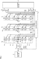
- Fig. 1 is a schematic configuration diagram of a power conversion device according to a first embodiment.
- the power conversion device includes leg circuits 8a, 8b, and 8c which are main circuits (which are denoted as a leg circuit 8 when they are collectively referred to or an unspecified one is referred to) and a control device 5 which controls these leg circuits 8.
- Leg circuit 8 is provided for each of a plurality of phases implementing an alternating current and connected between an AC circuit 2 and a DC circuit 4, and converts power between these circuits.
- Fig. 1 shows three-phase AC circuit 2, and three leg circuits 8a, 8b, and 8c corresponding to a u phase, a v phase, and a w phase, respectively, are provided.
- AC terminals Nu, Nv, and Nw provided in respective leg circuits 8a, 8b, and 8c are connected to AC circuit 2 with an interconnected transformer 3 being interposed.
- AC circuit 2 is, for example, an AC power system including an AC power supply.
- Fig. 1 does not show connection of AC terminals Nv and Nw to interconnected transformer 3.
- DC terminals Np and Nn (a positive-side DC terminal Np and a negative-side DC terminal Nn) provided in common to leg circuits 8 are connected to DC circuit 4.
- DC circuit 4 is, for example, a DC power system including a DC power grid and another power conversion device which provides a DC output.
- AC terminals Nu, Nv, and Nw may be connected to AC circuit 2 with an interconnected reactor being interposed.
- a primary winding may be provided in each of leg circuits 8a, 8b, and 8c, and leg circuits 8a, 8b, and 8c may be connected in an AC manner to interconnected transformer 3 or an interconnected reactor with a secondary winding magnetically coupled to the primary winding being interposed.
- the primary winding may be implemented by reactors 7a and 7b.
- Leg circuit 8 is electrically (in a DC or AC manner) connected to AC circuit 2 with a connection portion provided in each of leg circuits 8a, 8b, and 8c being interposed, such as AC terminals Nu, Nv, and Nw or the above-described primary winding.
- Leg circuit 8a is divided into a positive-side arm (which is also referred to as an upper arm or a primary arm) 13 from positive-side DC terminal Np to AC input terminal Nu and a negative-side arm (which is also referred to as a lower arm or a secondary arm) 14 from negative-side DC terminal Nn to AC input terminal Nu.
- a point of connection Nu between positive-side arm 13 and negative-side arm 14 is connected to transformer 3.
- Positive-side DC terminal Np and negative-side DC terminal Nn are connected to DC circuit 4. Since leg circuits 8b and 8c are also similarly configured, leg circuit 8a will be described below as a representative.
- Positive-side arm 13 includes a cell group 6a in which a plurality of converter cells 1 are cascaded, a cell group 6c in which a plurality of converter cells 1 are cascaded, and reactor 7a.
- Cell groups 6a and 6c and reactor 7a are connected in series to one another.
- a converter cell may be referred to as a cell below.
- Fig. 1 shows only a single cell 1 in cell group 6c for facilitating illustration, a plurality of cells 1 are actually cascaded.
- negative-side arm 14 includes a cell group 6b in which a plurality of cells 1 are cascaded, a cell group 6d in which a plurality of cells 1 are cascaded, and reactor 7b.
- Cell groups 6b and 6d and reactor 7b are connected in series to one another.
- Fig. 1 shows only a single cell 1 in cell group 6d for facilitating illustration, a plurality of cells 1 are actually cascaded.
- each cell 1 included in cell groups 6a and 6b is identical in configuration to each cell 1 included in cell groups 6c and 6d will mainly be described below. Unlike the former, each cell 1 included in cell groups 6a and 6b may be different in configuration from each cell 1 included in cell groups 6c and 6d. In any case, a function and effect is similar.
- Reactor 7a may be inserted in any position in positive-side arm 13 of leg circuit 8a, and reactor 7b may be inserted in any position in negative-side arm 14 of leg circuit 8a.
- a plurality of reactors 7a and a plurality of reactors 7b may be provided. The reactors may be different in inductance value. Only reactor 7a of positive-side arm 13 or only reactor 7b of negative-side arm 14 may be provided.
- Cell groups 6a and 6c provided in positive-side arm 13 are referred to as a positive-side cell group and cell groups 6b and 6d provided in negative-side arm 14 are referred to as a negative-side cell group.
- positive-side cell group 6a and negative-side cell group 6b are without being used for control of a circulating current but are used only for control of an AC electric quantity and a DC electric quantity.
- Positive-side cell group 6c and negative-side cell group 6d are used for control of a circulating current. Control of a circulating current is characterized in that only at least one cell constituting each leg circuit 8 is used therefor.
- the power conversion device in Fig. 1 further includes an AC voltage detector 10, DC voltage detectors 11a and 11b, and arm current detectors 9a and 9b provided in each leg circuit 8 as detectors which detect electric quantities (a current and a voltage) used for control. Signals detected by these detectors are input to control device 5.
- AC voltage detector 10 detects a U-phase voltage value Vacu, a V-phase voltage value Vacv, and a W-phase voltage value Vacw of AC circuit 2.
- DC voltage detector 11a detects a voltage of positive-side DC terminal Np connected to DC circuit 4.
- DC voltage detector 11b detects a voltage of negative-side DC terminal Nn connected to DC circuit 4.
- Arm current detectors 9a and 9b provided in leg circuit 8a for the U phase detect an arm current Ipu which flows in positive-side arm 13 and an arm current Inu which flows in negative-side arm 14, respectively.
- arm current detectors 9a and 9b provided in leg circuit 8b for the V phase detect a positive-side arm current Ipv and a negative-side arm current Inv, respectively.
- Arm current detectors 9a and 9b provided in leg circuit 8c for the W phase detect a positive-side arm current Ipw and a negative-side arm current Inw, respectively.
- Arm currents Ipu, Inu, Ipv, Inv, Ipw, and Inw which flow from positive-side DC terminal Np toward negative-side DC terminal Nn are defined as positive currents.
- Fig. 2 is a circuit diagram showing one example of a converter cell constituting cell groups 6a, 6b, 6c, and 6d.
- Converter cell 1 shown in Fig. 2 (A) adopts a half-bridge configuration and includes semiconductor switching elements 1a and 1b (which may hereinafter simply be referred to as a switching element) connected in series to each other, diodes 1c and 1d, and a DC capacitor 1e as an energy storage.
- Diodes 1c and 1d are connected in anti-parallel (in parallel and in a direction of a reverse bias) to switching elements 1a and 1b, respectively.
- DC capacitor 1e is connected in parallel to a series connection circuit of switching elements 1a and 1b and smoothes a DC voltage.
- a connection node between switching elements 1a and 1b is connected to a positive-side input and output terminal 1p and a connection node between switching element 1b and DC capacitor 1e is connected to a negative-side input and output terminal In.
- switching elements 1a and 1b are controlled such that one is turned on and the other is turned off.
- switching element 1a is turned on and switching element 1b is turned off, a voltage across opposing ends of DC capacitor 1e is applied across input and output terminals 1p and In (a positive-side voltage being applied to input and output terminal 1p and a negative-side voltage being applied to input and output terminal In).
- Converter cell 1 shown in Fig. 2 (A) can output a zero voltage or a positive voltage (dependent on a voltage of DC capacitor 1e) by alternately turning on switching elements 1a and 1b.
- Diodes 1c and 1d are provided for protection when voltages in reverse directions are applied to switching elements 1a and 1b.
- Converter cell 1 shown in Fig. 2 (B) adopts a full-bridge configuration and it is different from converter cell 1 in Fig. 2 (A) in further including switching elements 1f and 1g connected in series and diodes 1h and 1i connected in anti-parallel to switching elements 1f and 1g.
- Switching elements 1f and 1g as a whole are connected in parallel to the series connection circuit of switching elements 1a and 1b and connected in parallel to DC capacitor 1e.
- Input and output terminal 1p is connected to the connection node between switching elements 1a and 1b and input and output terminal 1n is connected to a connection node between switching elements 1f and 1g.
- Converter cell 1 shown in Fig. 2 (B) is controlled such that switching element 1g is normally turned on, switching element 1f is normally turned off, and switching elements 1a and 1b are alternately turned on during a normal operation (that is, a zero voltage or a positive voltage is output across input and output terminals 1p and In).
- Converter cell 1 shown in Fig. 2 (B) can also output a zero voltage or a negative voltage by turning off switching element 1g, turning on switching element If, and alternately turning on switching elements 1a and 1b.
- Converter cell 1 shown in Fig. 2 (C) is configured with switching element 1f having been removed from converter cell 1 of the full-bridge configuration shown in Fig. 2 (B) and it is otherwise the same as in Fig. 2 (B) .
- a converter cell configured as in Fig. 2 (C) is herein referred to as a hybrid type.
- Converter cell 1 in Fig. 2 (C) is controlled such that switching element 1g is normally turned on and switching elements 1a and 1b are alternately turned on during the normal operation (that is, a zero voltage or a positive voltage is output across input and output terminals 1p and In).
- Converter cell 1 shown in Fig. 2 (C) can output a negative voltage when switching elements 1a and 1g are turned off and switching element 1b is turned on so that a current flows from input and output terminal 1n toward input and output terminal 1p.
- a self-turn-off switching element capable of control of both of an on operation and an off operation is employed for each of switching elements 1a, 1b, 1f, and 1g.
- an insulated gate bipolar transistor (IGBT) or a gate commutated turn-off thyristor (GCT) is employed as switching elements 1a, 1b, 1f, and 1g.
- Fig. 3 is a block diagram showing an exemplary hardware configuration of the control device in Fig. 1 .
- Control device 5 in Fig. 3 is configured similarly to what is called a digital relay. Specifically, referring to Fig. 3 , control device 5 includes an analog-digital (AD) conversion unit 30, a processing unit 35, an input and output (IO) unit 43, and a setting and representation unit 47.
- AD analog-digital
- IO input and output
- a plurality of transformers that convert input signals from arm current detectors 9a and 9b, AC voltage detector 10, and DC voltage detectors 11a and 11b to a voltage level suitable for signal processing in control device 5 may be provided.
- AD conversion unit 30 includes an analog filter 31 and an AD converter 32.
- Analog filter 31 is implemented by a low pass filter provided to remove aliasing in AD conversion.
- AD converter 32 converts a signal that has passed through analog filter 31 to a digital value.
- AD conversion unit 30 includes a plurality of analog filters 31 and a multiplexer (not shown) for selection of signals that have passed through the plurality of analog filters 31.
- Processing unit 35 includes a central processing unit (CPU) 36, a memory 37, bus interfaces 38 and 39, and a bus 40 that connects these components to one another.
- CPU 36 controls operations by control device 5 as a whole.
- Memory 37 is used as a main storage of CPU 36.
- Memory 37 stores a program and a set value for signal processing by containing a non-volatile memory such as a flash memory.
- Processing unit 35 should only be implemented by a circuit with a processing function and is not limited to the example in Fig. 3 .
- processing unit 35 may include a plurality of CPUs.
- Processing unit 35 may be implemented by at least one application specific integrated circuit (ASIC) or at least one field programmable gate array (FPGA) instead of a processor such as the CPU.
- ASIC application specific integrated circuit
- FPGA field programmable gate array
- processing unit 35 may be implemented by combination of any of a processor, an ASIC, and an FPGA.
- IO unit 43 includes a communication circuit 44, a digital input circuit 45, and a digital output circuit 46.
- Communication circuit 44 generates an optical signal for output to each converter cell 1.
- a signal output from communication circuit 44 is transmitted to each converter cell 1 through an optical relay 55.
- Digital input circuit 45 and digital output circuit 46 are interface circuits in establishing communication between CPU 36 and an external apparatus. For example, digital output circuit 46 outputs a trip signal to a circuit breaker (not shown) provided between an AC power system 2 and the power conversion device.
- Setting and representation unit 47 includes a touch panel 48 for input and representation of a set value.
- Touch panel 48 is an input and output interface which is combination of a display such as a liquid crystal panel and an input apparatus such as a touch pad. Touch panel 48 is connected to bus 40 with bus interface 39 being interposed.
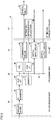
- Fig. 4 is a block diagram showing a functional configuration of the control device in Fig. 1 .
- a configuration of control device 5 and a general operation by each element will be described below with reference to Figs. 1 and 4 .
- Control device 5 includes a voltage command value generation unit 5z and gate controllers 5k, 5m, 5n, and 5o.
- Gate controller 5k supplies gate signals Gpu, Gpv, and Gpw to each switching element constituting positive-side cell group 6a of leg circuits 8a, 8b, and 8c, respectively.
- Gate controller 5m supplies gate signals Gnu, Gnv, and Gnw to each switching element constituting negative-side cell group 6b of leg circuits 8a, 8b, and 8c, respectively.
- Gate controller 5n supplies gate signals Gp2u, Gp2v, and Gp2w to each switching element constituting positive-side cell group 6c for control of a circulating current of leg circuits 8a, 8b, and 8c, respectively.
- Gate controller 5o supplies gate signals Gn2u, Gn2v, and Gn2w to each switching element constituting negative-side cell group 6d for control of a circulating current of leg circuits 8a, 8b, and 8c, respectively.
- Voltage command value generation unit 5z supplies voltage command values Vpref, Vnref, Vpref2, and Vnref2 to gate controllers 5k, 5m, 5n, and 5o, respectively. Voltage command values Vpref2 and Vnref2 supplied to respective gate controllers 5n and 5o for control of a circulating current are based on a detection value of a circulating current Icc. Voltage command values Vpref and Vnref supplied to other gate controllers 5k and 5m are not based on a detection value of circulating current Icc.
- voltage command value generation unit 5z includes a current calculator 5a, a circulating current controller 5b, an AC controller 5c, a DC controller 5d, command value combination units 5e and 5f, gain circuits 5g and 5h, and adders 5i and 5j.
- Current calculator 5a takes in positive-side arm currents Ipu, Ipv, and Ipw detected by current detector 9a provided in positive-side arm 13 of leg circuit 8 of each phase and negative-side arm currents Inu, Inv, and Inw detected by current detector 9b provided in negative-side arm 14 of leg circuit 8 of each phase.
- Current calculator 5a calculates AC current values Iacu, Iacv, and Iacw, a DC current value Idc, and circulating current values Iccu, Iccv, and Iccw from the arm current which has been taken in.
- Current calculator 5a outputs calculated AC current values Iacu, Iacv, and Iacw to AC controller 5c, outputs calculated DC current value Idc to DC controller 5d, and outputs calculated circulating current values Iccu, Iccv, and Iccw to circulating current controller 5b.
- U-phase AC current Iacu, V-phase AC current Iacv, and W-phase AC current Iacw (which are denoted as an AC current lac when they are collectively referred to) which flow from AC terminals Nu, Nv, and Nw of each leg circuit 8 toward transformer 3 are defined as positive.
- DC current Idc which flows from DC circuit 4 toward positive-side DC terminal Np and from negative-side DC terminal Nn toward DC circuit 4 is defined as positive.
- Circulating currents Iccu, Iccv, and Iccw which flow through leg circuits 8a, 8b, and 8c, respectively (which are denoted as circulating current Icc when they are collectively referred to) from positive-side DC terminal Np toward negative-side DC terminal Nn are defined as positive.
- AC voltage values Vacu, Vacv, and Vacw of the U phase, the V phase and the W phase (which are denoted as an AC voltage value Vac when they are collectively referred to) detected by AC voltage detector 10 are further input to AC controller 5c.
- AC controller 5c generates AC voltage command values Vacrefu, Vacrefv, and Vacrefw of the U phase, the V phase, and the W phase (which are denoted as an AC voltage command value Vacref when they are collectively referred to) based on input AC current value lac and AC voltage value Vac.
- DC voltage values Vdcp and Vdcn detected by DC voltage detectors 11a and 11b are further input to DC controller 5d.
- DC controller 5d generates a DC voltage command value Vdcref based on input DC voltage values Vdcp and Vdcn and DC current value Idc.
- Command value combination unit 5e generates a voltage command value Vprefu for U-phase positive-side cell group 6a by combining U-phase AC voltage command value Vacrefu and DC voltage command value Vdcref with each other. Similarly, command value combination unit 5e generates a voltage command value Vprefv for V-phase positive-side cell group 6a by combining V-phase AC voltage command value Vacrefv and DC voltage command value Vdcref with each other. Command value combination unit 5e further generates a voltage command value Vprefw for W-phase positive-side cell group 6a by combining W-phase AC voltage command value Vacrefw and DC voltage command value Vdcref with each other. Generated voltage command values Vprefu, Vprefv, and Vprefw (which are denoted as voltage command value Vpref when they are collectively referred to or an unspecified voltage command value is referred to) is input to gate controller 5k.
- Command value combination unit 5f generates a voltage command value Vnrefu for U-phase negative-side cell group 6b by combining U-phase AC voltage command value Vacrefu and DC voltage command value Vdcref with each other. Similarly, command value combination unit 5f generates a voltage command value Vnrefv for V-phase negative-side cell group 6b by combining V-phase AC voltage command value Vacrefv and DC voltage command value Vdcref with each other. Command value combination unit 5f further generates a voltage command value Vnrefw for W-phase negative-side cell group 6b by combining W-phase AC voltage command value Vacrefw and DC voltage command value Vdcref with each other.
- Generated voltage command values Vnrefu, Vnrefv, and Vnrefw (which are denoted as voltage command value Vnref when they are collectively referred to or an unspecified voltage command value is referred to) are input to gate controller 5m.
- Circulating current controller 5b generates voltage command values Vccrefu, Vccrefv, and Vccrefw (which are denoted as a voltage command value Vccref when they are collectively referred to or an unspecified voltage command value is referred to) for control of a circulating current of each phase based on respective circulating current values Iccu, Iccv, and Iccw.
- Generated voltage command value Vccref for control of a circulating current of each phase is added in adder 5i for each phase to voltage command value Vpref for positive-side cell group 6a which has been multiplied by a gain K.
- a voltage command value Vpref2 for positive-side cell group 6c for control of a circulating current is generated and generated voltage command value Vpref2 is supplied to gate controller 5n.
- generated voltage command value Vccref for control of a circulating current of each phase is added in adder 5j for each phase to voltage command value Vnref for negative-side cell group 6b which has been multiplied by gain K. Consequently, voltage command value Vnref2 for negative-side cell group 6d for control of a circulating current is generated and generated voltage command value Vnref2 is supplied to gate controller 5o.
- a voltage command value is added by adders 5i and 5j.
- a cell of a half bridge type is able to output only a zero voltage or a positive voltage, and in order to increase or lower an output voltage of converter cell 1 with increase and lowering in circulating current, the output voltage should be increased or lowered with a certain voltage value being defined as the reference.
- capacitor 1e is undesirably continuously charged with DC current Idc that flows between DC circuit 4 and leg circuit 8.
- voltage command values Vpref2 and Vnref2 for controlling cell groups 6c and 6d are generated by addition of a reference voltage which is K times as large as voltage command values Vpref and Vnref for cell groups 6a and 6b to voltage command value Vccref for circulating current control, respectively.
- a voltage of capacitor 1e in each converter cell 1 included in cell groups 6c and 6d can thus be maintained at a constant value.
- Proportional gain K is set to any value that will not saturate an output voltage of converter cell 1 when voltage command value Vccref for circulating current control is provided.
- the reference voltage can be set to 0 and hence proportional gain K can be set to 0.
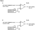
- Fig. 5 is a functional block diagram showing a detailed operation of a gate controller in Fig. 4 .
- Fig. 5 (A) shows a functional block diagram of gate controllers 5k and 5m and
- Fig. 5 (B) shows a functional block diagram of operations of gate controllers 5n and 5o.
- gate controller 5k provides corresponding gate signals Gpu, Gpv, and Gpw to the switching element of cell 1 constituting positive-side cell group 6a of each phase based on voltage command values Vprefu, Vprefv, and Vprefw of the U phase, the V phase, and the W phase combined by command value combination unit 5e.
- Gate controller 5m provides corresponding gate signals Gnu, Gnv, and Gnw to the switching element of cell 1 constituting negative-side cell group 6b of each phase based on voltage command values Vnrefu, Vnrefv, and Vnrefw of the U phase, the V phase, and the W phase combined by command value combination unit 5f.
- switching element 1a is turned on and switching element 1b is turned off when a voltage of DC capacitor 1e is output.
- switching element 1a is turned off and switching element 1b is turned on.
- a pulse width modulation (PWM) scheme is employed in the present embodiment as a scheme for controlling a converter which can output a binary voltage level. Under the pulse width modulation scheme, a pulse width of a gate signal supplied to a switching element is controlled such that a DC component of a desired voltage or an AC component of a fundamental wave can be output in a time average manner.
- each of gate controllers 5k and 5m for arm voltage control includes a comparator 70a and a carrier signal generator 71a.
- Carrier signal generator 71a generates, for example, a triangular carrier signal CS.
- Comparator 70a compares voltage command value Vpref or Vnref (which is denoted as a voltage command value Vref when voltage command values are collectively referred to) with carrier signal CS, and generates such a signal as attaining to the high level when voltage command value Vref is larger than carrier signal CS and attaining to the low level when voltage command value Vref is equal to or smaller than carrier signal CS, that is, a gate signal Gp or Gn.
- Fig. 6 is a schematic timing chart showing one example of a voltage command value and a carrier signal in Fig. 5 (A) .
- Fig. 6 shows exemplary carrier signals CSa to CSf under a phase shift PWM scheme when converter cell groups 6a and 6b for voltage control in each arm circuit include converter cells in six stages.
- the phase shift PWM scheme reduces a harmonic component of a combined voltage by shifting timing of a PWM signal output to each converter cell.
- Fig. 6 further shows exemplary voltage command value Vref output from command value combination unit 5e or 5f in Fig. 4 .
- a jagged shape like steps in accordance with a control processing cycle of command value combination unit 5e or 5f is observed in a waveform of voltage command value Vref. Therefore, as the control processing cycle is shorter, a smoother shape like a sinusoidal wave is obtained.
- Carrier signal CS generated by carrier signal generator 71a in Fig. 5 should have a frequency of magnitude of a non-integral multiple of a fundamental frequency of the AC power system, in order to suppress variation in voltage of a capacitor in each converter cell.
- Carrier signal CS desirably has a frequency of magnitude between three times and four times as high as the fundamental frequency of the AC power system.
- carrier signal CS has a frequency equal to or lower than three times as high as the fundamental frequency of the AC power system, control responsiveness is poorer and balance of a capacitor voltage among converter cells included in the arm is lost.
- carrier signal CS has a frequency at least four times as high as the fundamental frequency of the AC power system, switching loss increases.
- the frequency of carrier signal CS is set to 3.5 times as high as the frequency of voltage command value Vref.
- Gate controller 5n provides corresponding gate signals Gp2u, Gp2v, and Gp2w to the switching element of cell 1 constituting positive-side cell group 6c of the corresponding phase based on voltage command values Vpref2u, Vpref2v, and Vpref2w of the U phase, the V phase, and the W phase output from adder 5i.
- Gate controller 5o provides corresponding gate signals Gn2u, Gn2v, and Gn2w to the switching element of cell 1 constituting negative-side cell group 6d of each phase based on voltage command values Vnref2u, Vnref2v, and Vnref2w of the U phase, the V phase, and the W phase output from adder 5j.
- Gate controllers 5n and 5o are operated under the pulse width modulation scheme similarly to gate controllers 5k and 5m.
- each of gate controllers 5n and 5o for circulating current control includes a comparator 70b and a carrier signal generator 71b.
- Carrier signal generator 71b generates a triangular carrier signal CS2.
- Comparator 70b compares voltage command value Vpref 2 or Vnref 2 (which is denoted as a voltage command value Vref2 when voltage command values are collectively referred to) with carrier signal CS2, and generates such a signal as attaining to the high level when voltage command value Vref2 is larger than carrier signal CS2 and attaining to the low level when voltage command value Vref2 is equal to or smaller than carrier signal CS2, that is, a gate signal Gp2 or Gn2.
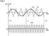
- Fig. 7 is a schematic timing chart showing one example of a voltage command value and a carrier signal in Fig. 5 (A) and one example of a carrier signal in Fig. 5 (B) .
- control stability is enhanced by quickly switching a control command value. For example, when balance of three-phase alternating current is suddenly lost due to occurrence of an AC system accident, higher control responsiveness provides higher followability to such an accidental phenomenon and hence control is further stabilized.
- a frequency of carrier signal CS2 used in gate controllers 5n and 5o for circulating current control is set to a value higher than a frequency of carrier signal CS used in gate controllers 5k and 5m for arm voltage control.
- the frequency of carrier signal CS shown in Fig. 7 is set to 3.5 times as high as the fundamental frequency of the AC power system (equal to the frequency of voltage command value Vref).
- the frequency of carrier signal CS2 shown in Fig. 7 is set to 10.5 times as high as the fundamental frequency of the AC power system.
- a time period from time t0 to time t1 and a time period from time t1 to time t2 each correspond to one cycle of the AC power system.
- a period of one cycle includes pulses of 3.5 carrier signals CS and pulses of 10.5 carrier signals CS2.
- leg circuit 8 corresponding to each phase of three-phase alternating current is provided with cell groups 6a and 6b used for arm voltage control and cell groups 6c and 6d used for a purpose other than arm voltage control (for example, circulating current control).
- a frequency of a PWM signal for control of each converter cell 1 included in cell groups 6c and 6d is set to a value higher than a frequency of a PWM signal for control of each converter cell 1 included in cell groups 6a and 6b.
- converter cells 1 included in cell groups 6a and 6b Depending on magnitude of a DC voltage or an AC voltage to be output, a necessary number of converter cells and spare converter cells are provided as converter cells 1 included in cell groups 6a and 6b such that a voltage applied to each converter cell 1 does not exceed a rated voltage.
- gate controllers 5k, 5m, 5n, and 5o are provided in control device 5
- gate controller 5k, 5m, 5n, or 5o may be provided in converter cell 1 included in corresponding one of cell groups 6a, 6b, 6c, and 6d.
- voltage command value generation unit 5z in Fig. 4 transmits voltage command values Vpref and Vnref to each converter cell 1 included in corresponding one of cell groups 6a and 6b and transmits voltage command values Vpref2 and Vnref2 to each converter cell 1 included in corresponding one of cell groups 6c and 6d.
- a configuration of converter cell 1 in this case will now be described.
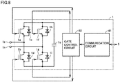
- Fig. 8 is a circuit diagram showing a modification of the converter cell in Fig. 2 (B) in the first embodiment.
- the converter cells in Fig. 2 (A) and (C) can also similarly be modified.
- Converter cell 1 in Fig. 8 is different from converter cell 1 in Fig. 2 (B) in further including a gate control circuit 60 and a communication circuit 61.
- Communication circuit 61 receives a corresponding voltage command value among voltage command values Vpref, Vnref, Vpref2, and Vnref2 by communicating with communication circuit 44 of control device 5 shown in Fig. 3 .
- Gate control circuit 60 corresponds to any of gate controllers 5k, 5m, 5n, and 5o in Fig. 4 .
- Gate control circuit 60 outputs a gate signal in accordance with the voltage command value received through communication circuit 61. Specifically, as described with reference to Fig. 5 , a PWM signal is generated based on comparison of the voltage command value with carrier signal CS or CS2.
- Control device 5 and converter cell 1 according to the configuration in the modification also achieve an effect the same as in the configuration in Fig. 4 described previously.
- each leg circuit 8 only reactor 7a on the positive side of reactors 7a and 7b may be provided or only reactor 7b on the negative side may be provided.
- positive-side cell group 6c for control of a circulating current is not required and gate controller 5n, adder 5i, and gain circuit 5g associated therewith are not required either, which is advantageous in simplification of the configuration of control device 5.
- negative-side cell group 6d for control of a circulating current is not required and gate controller 5o, adder 5j, and gain circuit 5h associated therewith are not required either, which is advantageous in simplification of the configuration of control device 5.
- Fig. 9 is a schematic configuration diagram of a power conversion device according to the second embodiment.
- the power conversion device in Fig. 9 is different from the power conversion device in Fig. 1 in including a control device 50 that controls cell groups 6a and 6b and a control device 51 that controls cell groups 6c and 6d.
- control device 50 and control device 51 includes, for example, the hardware configuration in Fig. 3 . From a point of view of functions, functions of control device 5 in Fig. 1 are shared between control device 50 and control device 51. Specifically, control device 50 and control device 51 perform functions shown in functional block diagrams in Figs. 10 and 11 , respectively.
- Fig. 10 is a block diagram showing a functional configuration of control device 50 in Fig. 9 .
- control device 50 in Fig. 9 includes current calculator 5a in Fig. 4 , a control unit 12a for arm voltage control, and gate controllers 5k and 5m.
- Current calculator 5a calculates AC current value lac and DC current value Idc based on arm currents Ip and In of each phase.
- Control unit 12a includes AC controller 5c, DC controller 5d, and command value combination units 5e and 5f in Fig. 4 .
- Control unit 12a generates voltage command values Vpref and Vnref based on AC voltage values Vacu, Vacv, and Vacw of respective phases detected by AC voltage detector 10 in Fig. 1 , DC voltage values Vdcp and Vdcn detected by DC voltage detectors 11a and 11b, and AC current value lac and DC current value Idc calculated by current calculator 5a.
- Fig. 11 is a block diagram showing a functional configuration of control device 51 in Fig. 9 .
- control device 51 in Fig. 9 includes current calculator 5a in Fig. 4 , a control unit 12b for circulating current control, and gate controllers 5n and 5o.
- Current calculator 5a calculates circulating current value Icc based on arm currents Ip and In of each phase.
- Control unit 12b includes circulating current controller 5b, gain circuits 5g and 5h, and adders 5i and 5j in Fig. 4 .
- gain circuits 5g and 5h and adders 5i and 5j do not have to be provided.
- Control unit 12b generates voltage command values Vpref2 and Vnref2 based on circulating current value Icc calculated by current calculator 5a.
- Fig. 12 is a schematic timing chart showing contents of processing by a CPU that implements control devices 50 and 51 in Fig. 9 .
- Fig. 12 (A) is a schematic timing chart showing contents of processing by control device 50 and
- Fig. 12 (C) is a schematic timing chart showing inside of processing by control device 51.
- Fig. 12 (B) is a timing chart when control device 50 performs contents of processing by control device 51.
- control device 50 performs processing 75a for converting an input signal into a signal for application calculation (which is referred to as input processing 75a below) and thereafter performs application calculation 76a (which is abbreviated as application calculation 76a).
- control device 50 calculates AC current value lac and DC current value Idc based on arm current values Ip and In of each phase. Control device 50 further generates voltage command values Vpref and Vnref based on AC voltage values Vacu, Vacv, and Vacw of respective phases, DC voltage values Vdcp and Vdcn detected by DC voltage detectors 11a and 11b, and calculated AC current value lac and DC current value Idc. Control device 50 further generates gate signals Gp and Gn of each phase based on voltage command values Vpref and Vnref.
- control device 50 performs processing for converting generated gate signals Gp and Gn of each phase into an output signal (which is referred to as output processing 77a below).
- a processing time period for input processing 75a, application calculation 76a, and output processing 77a correspond to a calculation processing cycle T1. Such calculation is repeated thereafter.
- control device 50 when control device 50 performs contents of processing by control device 51 (the same as the operations by control device 5 in Fig. 1 ), input processing 75b, application calculation 76b, and output processing 77b are performed in identical calculation processing cycle T1. Input processing 75b and output processing 77b are processing similar to input processing 75a and output processing 77a, respectively.
- control device 51 calculates circulating current value Icc based on arm current values Ip and In of each phase. Control device 51 further generates voltage command values Vpref2 and Vnref2 based on calculated circulating current value Icc. Control device 51 further generates gate signals Gp2 and Gn2 of each phase based on voltage command values Vpref2 and Vnref2. Since application calculation 76b is thus easier in calculation contents than application calculation 76a, application calculation 76b is shorter in calculation time period than application calculation 76a.
- a calculation processing cycle T2 can be shorter than calculation processing cycle T1. Since a cycle of update of voltage command values Vpref2 and Vnref2 is consequently shorter, stability in control of a circulating current or the like can be improved.
- a CPU that implements control device 51 may be changed to a CPU higher in calculation capability than a CPU of control device 50.
- a programmable logic device such as an FPGA may be employed for control device 51.
- calculation capability of control device 51 can be enhanced. Therefore, even though the number of converter cells 1 included in each of cell groups 6c and 6d is small, ability to control a circulating current or the like can be enhanced.
- a frequency of gate signals Gp2 and Gn2 for controlling cell groups 6c and 6d is higher than a frequency of gate signals Gp and Gn for controlling cell groups 6a and 6b.
- a plurality of CPUs may be provided in control device 5 in Fig. 1 , at least one first CPU may perform the function of control device 50 in Fig. 10 , and at least one second CPU different from the first CPU may perform the function of control device 51 in Fig. 11 .
- a PLD may be employed instead of the second CPU.
- a function and effect the same as in the second embodiment is achieved also by providing hardware components separate from each other in an identical control device.
- gate controller 5k, 5m, 5n, or 5o may be provided in converter cell 1 included in corresponding one of cell groups 6a, 6b, 6c, and 6d.
- control device 50 in Fig. 9 transmits voltage command value Vpref or Vnref to converter cell 1 included in corresponding one of cell groups 6a, 6b, 6c, and 6d.
- Control device 51 transmits Vpref2 and Vnref2 to converter cell 1 included in corresponding one of cell groups 6c and 6d.
- the configuration of converter cell 1 in this case is the same as described with reference to Fig. 8 .
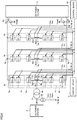
- Fig. 13 is a circuit diagram showing a configuration of converter cell 1 included in the other cell group 6c in upper arm 13 and the other cell group 6d in lower arm 14 in Fig. 1 .
- Converter cell 1 is configured to detect a voltage of DC capacitor 1e (a cell capacitor voltage Vccell) provided in the converter cell itself and to transmit a detection value to control device 5.
- DC capacitor 1e a cell capacitor voltage Vccell
- converter cell 1 in Fig. 13 is based on a full-bridge configuration converter cell 1 in Fig. 2 (B) and different from converter cell 1 in Fig. 2 (B) in further including a DC voltage detector 1j in parallel to DC capacitor 1e.
- DC voltage detector 1j detects voltage Vccell of DC capacitor 1e and outputs detected cell capacitor voltage Vccell to control device 5.
- switching elements 1a and 1b are used for circulating current control and not used for maintaining and controlling a voltage of DC capacitor 1e.
- switching elements 1g and 1f are used for control of a voltage of DC capacitor 1e and not used for circulating current control.
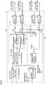
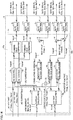
- Fig. 14 is a diagram of a configuration of control device 5 in Fig. 1 .
- Control device 5 shown in Fig. 14 may be implemented by a dedicated circuit, or may be implemented in part or in its entirety by a field programmable gate array (FPGA) and/or a microprocessor.
- FPGA field programmable gate array
- a configuration of control device 5 and a general operation by each element will be described below with reference to Figs. 1 and 14 .
- Control device 5 includes voltage command value generation unit 5z and gate controllers 5k, 5m, 5n, 5o, 5v, and 5w.
- Gate controllers 5k and 5m correspond to positive-side cell group 6a and negative-side cell group 6b of leg circuit 8 of each phase.
- Gate controller 5k generates gate signals Gpu, Gpv, and Gpw for control of switching elements included in positive-side cell groups 6a in respective leg circuits 8a, 8b, and 8c.
- Gate controller 5m generates gate signals Gnu, Gnv, and Gnw for control of switching elements included in negative-side cell groups 6b in respective leg circuits 8a, 8b, and 8c.
- Positive-side cell group 6c for circulating current control in leg circuit 8 of each phase corresponds to two gate controllers 5n and 5v and negative-side cell group 6d for circulating current control in leg circuit 8 of each phase corresponds to two gate controllers 5o and 5w.
- gate controller 5n generates gate signals Gp2u, Gp2v, and Gp2w for control of switching elements 1a and 1b provided in cell 1 in positive-side cell groups 6c in respective leg circuits 8a, 8b, and 8c.
- Gate controller 5o generates gate signals Gn2u, Gn2v, and Gn2w for control of switching elements 1a and 1b provided in cell 1 in negative-side cell groups 6d in respective leg circuits 8a, 8b, and 8c.
- Gate controller 5v generates gate signals Gp3u, Gp3v, and Gp3w for control of switching elements 1g and 1f provided in cell 1 in positive-side cell groups 6c in respective leg circuits 8a, 8b, and 8c.
- Gate controller 5w generates gate signals Gn3u, Gn3v, and Gn3w for control of switching elements 1g and 1f provided in cell 1 in negative-side cell groups 6d in respective leg circuits 8a, 8b, and 8c.
- Voltage command value generation unit 5z supplies a voltage command value to gate controllers 5k, 5m, 5n, 5o, 5v, and 5w.
- voltage command value generation unit 5z includes current calculator 5a, circulating current controller 5b, AC controller 5c, DC controller 5d, command value combination units 5e and 5f, a voltage calculator 5p, capacitor voltage controllers 5q and 5r, adders 5i, 5t, and 5u, and a gain circuit 5s.
- Current calculator 5a takes in positive-side arm currents Ipu, Ipv, and Ipw detected by current detector 9a provided in positive-side arm 13 of leg circuit 8 of each phase and negative-side arm currents Inu, Inv, and Inw detected by current detector 9b provided in negative-side arm 14 of leg circuit 8 of each phase.
- Current calculator 5a calculates AC current values Iacu, Iacv, and Iacw, DC current value Idc, and circulating current values Iccu, Iccv, and Iccw based on the arm currents that have been taken in.
- Current calculator 5a outputs calculated AC current values Iacu, Iacv, and Iacw to AC controller 5c, outputs calculated DC current value Idc to DC controller 5d, and outputs calculated circulating current values Iccu, Iccv, and Iccw to circulating current controller 5b.
- Current calculator 5a further outputs a result of multiplication by gain circuit 5s of calculated AC current values Iacu, Iacv, and Iacw by -1 to capacitor voltage controller 5q, and outputs calculated AC current values Iacu, Iacv, and Iacw to capacitor voltage controller 5r.
- U-phase AC current Iacu, V-phase AC current Iacv, and W-phase AC current Iacw (denoted as AC current lac when they are collectively referred to) that flow from AC terminals Nu, Nv, and Nw of leg circuit 8 toward transformer 3 are defined as positive.
- Circulating currents Iccu, Iccv, and Iccw (which are denoted as circulating current Icc when they are collectively referred to) that flow through leg circuits 8a, 8b, and 8c from positive-side DC terminal Np toward negative-side DC terminal Nn are defined as positive.
- U-phase, V-phase, and W-phase AC voltage values Vacu, Vacv, and Vacw (which are denoted as AC voltage value Vac when they are collectively referred to) detected by AC voltage detector 10 are input to AC controller 5c.
- AC controller 5c generates U-phase, V-phase, and W-phase AC voltage command values Vacrefu, Vacrefv, and Vacrefw (which are denoted as AC voltage command value Vacref when they are collectively referred to) based on input AC current value lac and AC voltage value Vac.
- DC voltage values Vdcp and Vdcn detected by DC voltage detectors 11a and 11b are further input to DC controller 5d.
- DC controller 5d generates DC voltage command value Vdcref based on input DC voltage values Vdcp and Vdcn and DC current value Idc.
- Command value combination unit 5e generates voltage command value Vprefu for U-phase positive-side cell group 6a by combining U-phase AC voltage command value Vacrefu and DC voltage command value Vdcref. Similarly, command value combination unit 5e generates voltage command value Vprefv for V-phase positive-side cell group 6a by combining V-phase AC voltage command value Vacrefv and DC voltage command value Vdcref. Command value combination unit 5e further generates voltage command value Vprefw for W-phase positive-side cell group 6a by combining W-phase AC voltage command value Vacrefw and DC voltage command value Vdcref. Generated voltage command values Vprefu, Vprefv, and Vprefw (which are denoted as voltage command value Vpref when they are collectively referred to or when an unspecified voltage command value is referred to) are input to gate controller 5k.
- Command value combination unit 5f generates voltage command value Vnrefu for U-phase negative-side cell group 6b by combining U-phase AC voltage command value Vacrefu and DC voltage command value Vdcref. Similarly, command value combination unit 5f generates voltage command value Vnrefv for V-phase negative-side cell group 6b by combining V-phase AC voltage command value Vacrefv and DC voltage command value Vdcref. Command value combination unit 5f further generates voltage command value Vnrefw for W-phase negative-side cell group 6b by combining W-phase AC voltage command value Vacrefw and DC voltage command value Vdcref.
- Generated voltage command values Vnrefu, Vnrefv, and Vnrefw (which are denoted as voltage command value Vnref when they are collectively referred to or when an unspecified voltage command value is referred to) are input to gate controller 5m.
- Circulating current controller 5b generates voltage command values Vccrefu, Vccrefv, and Vccrefw (which are denoted as voltage command value Vccref when they are collectively referred to or when an unspecified voltage command value is referred to) for control of circulating currents of respective phases based on respective circulating current values Iccu, Iccv, and Iccw.
- a bias value Vbias1 is added to generated voltage command value Vccref for circulating current control of each phase by adder 5i, and thereafter the resultant voltage command value is input to gate controllers 5n and 5o.
- Voltage calculator 5p receives information on cell capacitor voltage Vccell from each cell 1 provided in cell groups 6c and 6d of leg circuits 8a, 8b, and 8c of the respective phases shown in Fig. 1 .
- Voltage calculator 5p calculates a representative value Vcp (Vcpu of the U phase, Vcpv of the V phase, and Vcpw of the W phase) of a plurality of cell capacitor voltages of positive-side cell group 6c for each of the U phase, the V phase, and the W phase based on received information on cell capacitor voltage Vccell and calculates a representative value Vcn (Vcnu of the U phase, Vcnv of the V phase, and Vcnw of the W phase) of a plurality of cell capacitor voltages of negative-side cell group 6d.
- Voltage calculator 5p outputs representative values Vcpu, Vcpv, and Vcpw of the cell capacitor voltages of each positive-side cell group 6c to capacitor voltage controller 5q and representative values Vcnu, Vcnv, and Vcnw of the cell capacitor voltages of each negative-side cell group 6d to capacitor voltage controller 5r.
- Capacitor voltage controller 5q receives information on cell capacitor voltage values Vcpu, Vcpv, and Vcpw of positive-side cell group 6c from voltage calculator 5p and receives information on AC current values (-Iacu, -Iacv, and -Iacw) opposite in phase (that is, multiplied by -1) from current calculator 5a.
- Capacitor voltage controller 5q generates voltage command value Vcpref (Vcprefu for the U phase, Vcprefv for the V phase, and Vcprefw for the W phase) for control of a capacitor voltage of each cell 1 in positive-side cell group 6c based on the received information.
- a bias value Vbias 2 is added to generated voltage Vcpref by adder 5t, and thereafter the resultant voltage is input to gate controller 5v.
- Capacitor voltage controller 5r receives information on cell capacitor voltage values Vcnu, Vcnv, and Vcnw of negative-side cell group 6d from voltage calculator 5p and receives information on AC current values Iacu, Iacv, and Iacw from current calculator 5a.
- Capacitor voltage controller 5r generates voltage command value Vcnref (Vcnrefu for the U phase, Vcnrefv for the V phase, and Vcnrefw for the W phase) for control of a capacitor voltage of each cell 1 in negative-side cell group 6d based on the received information.
- Bias value Vbias2 is added to generated voltage Vcnref by adder 5u and the resultant voltage is input to gate controller 5w.
- Gate controller 5k provides corresponding one of gate signals Gpu, Gpv, and Gpw to a switching element in cell 1 included in positive-side cell group 6a of a corresponding phase based on U-phase, V-phase, and W-phase voltage command values Vprefu, Vprefv, and Vprefw combined by command value combination unit 5e.
- Gate controller 5m provides corresponding one of gate signals Gnu, Gnv, and Gnw to a switching element in cell 1 included in negative-side cell group 6b of a corresponding phase based on U-phase, V-phase, and W-phase voltage command values Vnrefu, Vnrefv, and Vnrefw combined by command value combination unit 5f.
- a pulse width modulation (PWM) scheme is employed in the present embodiment as a scheme for controlling a converter which can output a binary voltage level.
- Gate controllers 5n and 5o output a gate signal for control of switching of switching elements 1a and 1b provided in each cell 1 in cell groups 6c and 6d in accordance with a result of addition of voltage command value Vccref and bias value Vbias1.
- Gate controllers 5n and 5o can be operated under the pulse width modulation scheme similarly to gate controllers 5k and 5m.
- Circulating current Icc is a bipolar signal that has positive and negative values. Therefore, voltage command value Vccref output from circulating current controller 5b is also a bipolar signal.
- a duty factor (duty) of switching elements 1a and 1b is desirably set to 50% when voltage command value Vccref is 0.
- adder 5i adds bias value Vbias 1 to voltage command value Vccref.
- Circulating current Icc is equal in value between positive-side cell group 6c and negative-side cell group 6d. Therefore, common voltage command value Vccref is provided to gate controllers 5n and 5o.
- circulating current controllability can be enhanced by setting a frequency of a PWM signal generated by gate controllers 5n and 5o to be higher than a frequency of a PWM signal generated by gate controllers 5k and 5m.
- Gate controller 5v outputs a gate signal for control of switching of switching elements 1f and 1g provided in each cell 1 in cell group 6c in accordance with a result of addition of voltage command value Vcpref and bias value Vbias2.
- Gate controller 5v can be operated under the pulse width modulation scheme similarly to gate controllers 5k and 5m.
- gate controller 5w outputs a gate signal for control of switching of switching elements 1f and 1g provided in each cell 1 in cell group 6d in accordance with a result of addition of voltage command value Vcnref and bias value Vbias2.
- Gate controller 5w can be operated under the pulse width modulation scheme similarly to gate controllers 5k and 5m.
- bias value Vbias2 When bias value Vbias2 is set to a value as large as bias value Vbias1, in a full-bridge configuration like cell 1 shown in Fig. 13 , a duty factor is identical among switching elements 1a, 1b, 1f, and 1g while the circulating current is 0. Consequently, a time average value of an output voltage across input and output terminals 1p and 1n is zero and DC capacitor 1e is not charged or discharged even though a current flows. Since a voltage output from cell 1 in accordance with voltage command value Vccref output from circulating current controller 5b is applied to reactors 7a and 7b, a reactive power component is dominant.
- a PWM signal generated by gate controllers 5v and 5w may be equal to or different from a PWM signal generated by gate controllers 5n and 5o in frequency.
- a plurality of CPUs may be provided in control device 5 in Fig. 1 , at least one first CPU may perform calculation relating to voltage command values Vpref and Vnref, and at least one second CPU may perform calculation relating to voltage command values Vccref, Vcpref, and Vcnref.
- the second CPU may be higher in calculation capability than the first CPU, or a PLD may be employed instead of the second CPU.
- gate controllers 5k, 5m, 5n, 5o, 5v, and 5w may be provided in converter cell 1 included in corresponding one of cell groups 6a, 6b, 6c, and 6d.
- voltage command value generation unit 5z in Fig. 14 may transmit voltage command value Vpref or Vnref to converter cell 1 included in corresponding one of cell groups 6a and 6b and transmits voltage command values Vccref, Vcpref, and Vcnref to converter cell 1 included in corresponding one of cell groups 6c and 6d.
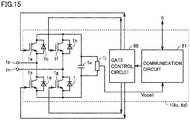
- Fig. 15 is a circuit diagram showing a modification of the converter cell in Fig. 13 in the third embodiment.
- the converter cells in Fig. 2 (A) and (C) can also similarly be modified.
- Converter cell 1 in Fig. 15 is different form converter cell 1 in Fig. 2 (B) in further including gate control circuit 60 and communication circuit 61.
- Communication circuit 61 receives a corresponding voltage command value among voltage command values Vpref, Vnref, Vccref, Vcpref, and Vcnref by communicating with communication circuit 44 of control device 5 shown in Fig. 3 .
- Communication circuit 61 transmits voltage Vccell of DC capacitor 1e detected by DC voltage detector 1j to communication circuit 44 of control device 5.
- gate control circuit 60 corresponds to gate controller 5k in Fig. 14 .
- gate control circuit 60 corresponds to gate controller 5m in Fig. 14 .
- gate control circuit 60 corresponds to gate controllers 5n and 5v in Fig. 14 .
- gate control circuit 60 corresponds to gate controllers 5o and 5w in Fig. 14 .
- Gate control circuit 60 outputs a gate signal in accordance with a voltage command value received through communication circuit 61. Specifically, a PWM signal is generated based on comparison of a voltage command value with carrier signal CS or carrier signal CS2 as described with reference to Fig. 5 .
- Control device 5 and converter cell 1 according to the configuration in the modification also achieve an effect the same as in Fig. 14 described previously.
- 1 converter cell 1a, 1b, 1f, 1g switching element; 1c, 1d, 1h, 1i diode; 1e DC capacitor; 1j, 11a, 11b DC voltage detector; In, 1p input and output terminal; 2 AC power system (AC circuit); 3 interconnected transformer; 4 DC power system (DC circuit); 5, 50, 51 control device; 5a current calculator; 5b circulating current controller; 5c AC controller; 5d DC controller; 5e, 5f command value combination unit; 5k, 5m, 5n, 5o, 5v, 5w gate controller; 5p voltage calculator; 5q, 5r capacitor voltage controller; 5z voltage command value generation unit; 6a, 6b, 6c, 6d cell group; 8a, 8b, 8c leg circuit; 9a, 9b arm current detector; 10 AC voltage detector; 12a, 12b control unit; 13 positive-side arm; 14 negative-side arm; 36 CPU; 60 gate control circuit; 70a, 70b comparator; 71, 71a, 71b carrier signal generator; CS, CS
Landscapes
- Engineering & Computer Science (AREA)
- Power Engineering (AREA)
- Inverter Devices (AREA)
- Rectifiers (AREA)
Abstract
Description
- The present disclosure relates to a power conversion device which converts power between an alternating current (AC) circuit and a direct current (DC) circuit and is used, for example, in a power system.
- In a power conversion device of a large capacity installed in a power system in recent years, instead of a separately-excited converter including a thyristor as a switching element, a self-excited converter including an insulated gate bipolar transistor as a switching element has generally been used. A modular multilevel converter (MMC) represents the self-excited converter.
- The modular multilevel converter includes a first arm connected to a DC terminal on a positive-electrode side and a second arm connected to a DC terminal on a negative-electrode side for each phase of a three-phase alternating current and each arm is configured with a plurality of converter cells (which are also referred to as sub modules or chopper cells) being cascaded. The first arm and the second arm of each phase implement a leg.
- Japanese National Patent Publication No.
2013-507100 - PTL 1: Japanese National Patent Publication No.
2013-507100 - The inventors of the present application have studied about a method of enhancing control stability of an MMC when each leg is configured with a first group of converter cells and a second group of converter cells as in
PTL 1. In particular, the inventors of the present application have studied about controllability of a group of converter cells that is not involved with a basic function for a conversion operation but is used for improvement in function of the MMC. The inventors of the present application have discussed a method allowing accurate control of a circulating current even though the group of converter cells includes a small number of converter cells, and derived the technique in the present disclosure.PTL 1 fails to mention such improvement in controllability of an MMC. - Therefore, an object of the present disclosure is to enhance controllability of a power conversion device under an MMC scheme including a plurality of groups of converter cells.
- The present disclosure is not limited to the embodiment disclosed in
PTL 1. For example, in a power conversion device according to the present disclosure, both of a first group and a second group may include half-bridge converter cells or full-bridge converter cells. - In one embodiment, a power conversion device that converts power between a DC circuit and an AC circuit includes a plurality of leg circuits connected in parallel between a first DC terminal and a second DC terminal and electrically connected to the AC circuit. Each of the plurality of leg circuits includes at least one first converter cell and a plurality of second converter cells other than the former. Each of the at least one first converter cell and the plurality of second converter cells includes a capacitor and a plurality of semiconductor switching elements. A first control signal that controls switching of each of the semiconductor switching elements included in the at least one first converter cell is higher in frequency than a second control signal that controls switching of each of the semiconductor switching elements included in each of the plurality of second converter cells.
- According to the embodiment, controllability of the power conversion device can be enhanced by setting a frequency of the first control signal to be higher than a frequency of the second control signal.
-
-
Fig. 1 is a schematic configuration diagram of a power conversion device according to a first embodiment. -
Fig. 2 is a circuit diagram showing one example of a converter cell included in each ofgroups -
Fig. 3 is a block diagram showing an exemplary hardware configuration of a control device inFig. 1 . -
Fig. 4 is a block diagram showing a functional configuration of the control device inFig. 1 . -
Fig. 5 is a functional block diagram showing a detailed operation by a gate controller inFig. 4 . -
Fig. 6 is a schematic timing chart showing one example of a voltage command value and a carrier signal inFig. 5 (A) . -
Fig. 7 is a schematic timing chart showing one example of a voltage command value and a carrier signal inFig. 5 (A) and one example of a carrier signal inFig. 5 (B) . -
Fig. 8 is a circuit diagram showing a modification of the converter cell inFig. 2 (B) in the first embodiment. -
Fig. 9 is a schematic configuration diagram of a power conversion device according to a second embodiment. -
Fig. 10 is a block diagram showing a functional configuration of acontrol device 50 inFig. 9 . -
Fig. 11 is a block diagram showing a functional configuration of acontrol device 51 inFig. 9 . -
Fig. 12 is a schematic timing chart showing contents of processing by a CPU that implementscontrol devices Fig. 9 . -
Fig. 13 is a circuit diagram showing a configuration of aconverter cell 1 included in theother cell group 6c in anupper arm 13 and theother cell group 6d in alower arm 14 inFig. 1 . -
Fig. 14 is a configuration diagram of acontrol device 5 inFig. 1 . -
Fig. 15 is a circuit diagram showing a modification of the converter cell inFig. 13 in a third embodiment. - Each embodiment will be described below in detail with reference to the drawings. The same or corresponding elements have the same reference characters allotted and description thereof will not be repeated.
-
Fig. 1 is a schematic configuration diagram of a power conversion device according to a first embodiment. Referring toFig. 1 , the power conversion device includesleg circuits control device 5 which controls these leg circuits 8. - Leg circuit 8 is provided for each of a plurality of phases implementing an alternating current and connected between an AC circuit 2 and a
DC circuit 4, and converts power between these circuits.Fig. 1 shows three-phase AC circuit 2, and threeleg circuits - AC terminals Nu, Nv, and Nw provided in
respective leg circuits transformer 3 being interposed. AC circuit 2 is, for example, an AC power system including an AC power supply. For facilitating illustration,Fig. 1 does not show connection of AC terminals Nv and Nw to interconnectedtransformer 3. DC terminals Np and Nn (a positive-side DC terminal Np and a negative-side DC terminal Nn) provided in common to leg circuits 8 are connected toDC circuit 4.DC circuit 4 is, for example, a DC power system including a DC power grid and another power conversion device which provides a DC output. - Instead of interconnected
transformer 3 inFig. 1 , AC terminals Nu, Nv, and Nw may be connected to AC circuit 2 with an interconnected reactor being interposed. Instead of AC terminals Nu, Nv, and Nw, a primary winding may be provided in each ofleg circuits leg circuits transformer 3 or an interconnected reactor with a secondary winding magnetically coupled to the primary winding being interposed. In this case, the primary winding may be implemented byreactors leg circuits -
Leg circuit 8a is divided into a positive-side arm (which is also referred to as an upper arm or a primary arm) 13 from positive-side DC terminal Np to AC input terminal Nu and a negative-side arm (which is also referred to as a lower arm or a secondary arm) 14 from negative-side DC terminal Nn to AC input terminal Nu. A point of connection Nu between positive-side arm 13 and negative-side arm 14 is connected totransformer 3. Positive-side DC terminal Np and negative-side DC terminal Nn are connected toDC circuit 4. Sinceleg circuits leg circuit 8a will be described below as a representative. - Positive-
side arm 13 includes acell group 6a in which a plurality ofconverter cells 1 are cascaded, acell group 6c in which a plurality ofconverter cells 1 are cascaded, andreactor 7a.Cell groups reactor 7a are connected in series to one another. For the sake of brevity, a converter cell may be referred to as a cell below. ThoughFig. 1 shows only asingle cell 1 incell group 6c for facilitating illustration, a plurality ofcells 1 are actually cascaded. - Similarly, negative-
side arm 14 includes acell group 6b in which a plurality ofcells 1 are cascaded, acell group 6d in which a plurality ofcells 1 are cascaded, andreactor 7b.Cell groups reactor 7b are connected in series to one another. ThoughFig. 1 shows only asingle cell 1 incell group 6d for facilitating illustration, a plurality ofcells 1 are actually cascaded. - An example in which each
cell 1 included incell groups cell 1 included incell groups cell 1 included incell groups cell 1 included incell groups -
Reactor 7a may be inserted in any position in positive-side arm 13 ofleg circuit 8a, andreactor 7b may be inserted in any position in negative-side arm 14 ofleg circuit 8a. A plurality ofreactors 7a and a plurality ofreactors 7b may be provided. The reactors may be different in inductance value. Onlyreactor 7a of positive-side arm 13 or onlyreactor 7b of negative-side arm 14 may be provided. -
Cell groups side arm 13 are referred to as a positive-side cell group andcell groups side arm 14 are referred to as a negative-side cell group. As will be described in detail below, positive-side cell group 6a and negative-side cell group 6b are without being used for control of a circulating current but are used only for control of an AC electric quantity and a DC electric quantity. Positive-side cell group 6c and negative-side cell group 6d are used for control of a circulating current. Control of a circulating current is characterized in that only at least one cell constituting each leg circuit 8 is used therefor. - The power conversion device in
Fig. 1 further includes anAC voltage detector 10,DC voltage detectors current detectors device 5. - Specifically,
AC voltage detector 10 detects a U-phase voltage value Vacu, a V-phase voltage value Vacv, and a W-phase voltage value Vacw of AC circuit 2.DC voltage detector 11a detects a voltage of positive-side DC terminal Np connected toDC circuit 4.DC voltage detector 11b detects a voltage of negative-side DC terminal Nn connected toDC circuit 4. Armcurrent detectors leg circuit 8a for the U phase detect an arm current Ipu which flows in positive-side arm 13 and an arm current Inu which flows in negative-side arm 14, respectively. Similarly, armcurrent detectors leg circuit 8b for the V phase detect a positive-side arm current Ipv and a negative-side arm current Inv, respectively. Armcurrent detectors leg circuit 8c for the W phase detect a positive-side arm current Ipw and a negative-side arm current Inw, respectively. Arm currents Ipu, Inu, Ipv, Inv, Ipw, and Inw which flow from positive-side DC terminal Np toward negative-side DC terminal Nn are defined as positive currents. -
Fig. 2 is a circuit diagram showing one example of a converter cell constitutingcell groups Converter cell 1 shown inFig. 2 (A) adopts a half-bridge configuration and includessemiconductor switching elements diodes DC capacitor 1e as an energy storage.Diodes elements DC capacitor 1e is connected in parallel to a series connection circuit of switchingelements elements output terminal 1p and a connection node between switchingelement 1b andDC capacitor 1e is connected to a negative-side input and output terminal In. - In the configuration in
Fig. 2 (A) , switchingelements element 1a is turned on and switchingelement 1b is turned off, a voltage across opposing ends ofDC capacitor 1e is applied across input andoutput terminals 1p and In (a positive-side voltage being applied to input andoutput terminal 1p and a negative-side voltage being applied to input and output terminal In). In contrast, when switchingelement 1a is turned off and switchingelement 1b is turned on, 0 V is applied across input andoutput terminals 1p and In.Converter cell 1 shown inFig. 2 (A) can output a zero voltage or a positive voltage (dependent on a voltage ofDC capacitor 1e) by alternately turning on switchingelements Diodes elements -
Converter cell 1 shown inFig. 2 (B) adopts a full-bridge configuration and it is different fromconverter cell 1 inFig. 2 (A) in further includingswitching elements diodes elements Switching elements elements DC capacitor 1e. Input andoutput terminal 1p is connected to the connection node between switchingelements output terminal 1n is connected to a connection node between switchingelements -
Converter cell 1 shown inFig. 2 (B) is controlled such that switchingelement 1g is normally turned on, switchingelement 1f is normally turned off, and switchingelements output terminals 1p and In).Converter cell 1 shown inFig. 2 (B) , however, can also output a zero voltage or a negative voltage by turning off switchingelement 1g, turning on switching element If, and alternately turning on switchingelements -
Converter cell 1 shown inFig. 2 (C) is configured with switchingelement 1f having been removed fromconverter cell 1 of the full-bridge configuration shown inFig. 2 (B) and it is otherwise the same as inFig. 2 (B) . A converter cell configured as inFig. 2 (C) is herein referred to as a hybrid type. -
Converter cell 1 inFig. 2 (C) is controlled such that switchingelement 1g is normally turned on and switchingelements output terminals 1p and In).Converter cell 1 shown inFig. 2 (C) can output a negative voltage when switchingelements element 1b is turned on so that a current flows from input andoutput terminal 1n toward input andoutput terminal 1p. - A self-turn-off switching element capable of control of both of an on operation and an off operation is employed for each of switching
elements elements -
Fig. 3 is a block diagram showing an exemplary hardware configuration of the control device inFig. 1 . -
Control device 5 inFig. 3 is configured similarly to what is called a digital relay. Specifically, referring toFig. 3 ,control device 5 includes an analog-digital (AD)conversion unit 30, aprocessing unit 35, an input and output (IO)unit 43, and a setting andrepresentation unit 47. - In a stage preceding
AD conversion unit 30, a plurality of transformers (not shown) that convert input signals from armcurrent detectors AC voltage detector 10, andDC voltage detectors control device 5 may be provided. -
AD conversion unit 30 includes ananalog filter 31 and anAD converter 32.Analog filter 31 is implemented by a low pass filter provided to remove aliasing in AD conversion.AD converter 32 converts a signal that has passed throughanalog filter 31 to a digital value. - Though
Fig. 3 representatively shows only one input channel ofAD conversion unit 30, the AD conversion unit is actually in a multi-input configuration for receiving signals from detectors. Therefore, more specifically,AD conversion unit 30 includes a plurality of analog filters 31 and a multiplexer (not shown) for selection of signals that have passed through the plurality of analog filters 31. - Processing
unit 35 includes a central processing unit (CPU) 36, amemory 37, bus interfaces 38 and 39, and abus 40 that connects these components to one another.CPU 36 controls operations bycontrol device 5 as a whole.Memory 37 is used as a main storage ofCPU 36.Memory 37 stores a program and a set value for signal processing by containing a non-volatile memory such as a flash memory. - Processing
unit 35 should only be implemented by a circuit with a processing function and is not limited to the example inFig. 3 . For example, processingunit 35 may include a plurality of CPUs. Processingunit 35 may be implemented by at least one application specific integrated circuit (ASIC) or at least one field programmable gate array (FPGA) instead of a processor such as the CPU. Alternatively, processingunit 35 may be implemented by combination of any of a processor, an ASIC, and an FPGA. -
IO unit 43 includes acommunication circuit 44, adigital input circuit 45, and adigital output circuit 46.Communication circuit 44 generates an optical signal for output to eachconverter cell 1. A signal output fromcommunication circuit 44 is transmitted to eachconverter cell 1 through anoptical relay 55.Digital input circuit 45 anddigital output circuit 46 are interface circuits in establishing communication betweenCPU 36 and an external apparatus. For example,digital output circuit 46 outputs a trip signal to a circuit breaker (not shown) provided between an AC power system 2 and the power conversion device. - Setting and
representation unit 47 includes atouch panel 48 for input and representation of a set value.Touch panel 48 is an input and output interface which is combination of a display such as a liquid crystal panel and an input apparatus such as a touch pad.Touch panel 48 is connected tobus 40 withbus interface 39 being interposed. -
Fig. 4 is a block diagram showing a functional configuration of the control device inFig. 1 . A configuration ofcontrol device 5 and a general operation by each element will be described below with reference toFigs. 1 and4 . -
Control device 5 includes a voltage commandvalue generation unit 5z andgate controllers Gate controller 5k supplies gate signals Gpu, Gpv, and Gpw to each switching element constituting positive-side cell group 6a ofleg circuits Gate controller 5m supplies gate signals Gnu, Gnv, and Gnw to each switching element constituting negative-side cell group 6b ofleg circuits Gate controller 5n supplies gate signals Gp2u, Gp2v, and Gp2w to each switching element constituting positive-side cell group 6c for control of a circulating current ofleg circuits side cell group 6d for control of a circulating current ofleg circuits - Voltage command
value generation unit 5z supplies voltage command values Vpref, Vnref, Vpref2, and Vnref2 togate controllers respective gate controllers 5n and 5o for control of a circulating current are based on a detection value of a circulating current Icc. Voltage command values Vpref and Vnref supplied toother gate controllers - More specifically, voltage command
value generation unit 5z includes acurrent calculator 5a, a circulatingcurrent controller 5b, anAC controller 5c, aDC controller 5d, commandvalue combination units gain circuits adders 5i and 5j. -
Current calculator 5a takes in positive-side arm currents Ipu, Ipv, and Ipw detected bycurrent detector 9a provided in positive-side arm 13 of leg circuit 8 of each phase and negative-side arm currents Inu, Inv, and Inw detected bycurrent detector 9b provided in negative-side arm 14 of leg circuit 8 of each phase.Current calculator 5a calculates AC current values Iacu, Iacv, and Iacw, a DC current value Idc, and circulating current values Iccu, Iccv, and Iccw from the arm current which has been taken in.Current calculator 5a outputs calculated AC current values Iacu, Iacv, and Iacw toAC controller 5c, outputs calculated DC current value Idc toDC controller 5d, and outputs calculated circulating current values Iccu, Iccv, and Iccw to circulatingcurrent controller 5b. - U-phase AC current Iacu, V-phase AC current Iacv, and W-phase AC current Iacw (which are denoted as an AC current lac when they are collectively referred to) which flow from AC terminals Nu, Nv, and Nw of each leg circuit 8 toward
transformer 3 are defined as positive. DC current Idc which flows fromDC circuit 4 toward positive-side DC terminal Np and from negative-side DC terminal Nn towardDC circuit 4 is defined as positive. Circulating currents Iccu, Iccv, and Iccw which flow throughleg circuits - AC voltage values Vacu, Vacv, and Vacw of the U phase, the V phase and the W phase (which are denoted as an AC voltage value Vac when they are collectively referred to) detected by
AC voltage detector 10 are further input toAC controller 5c.AC controller 5c generates AC voltage command values Vacrefu, Vacrefv, and Vacrefw of the U phase, the V phase, and the W phase (which are denoted as an AC voltage command value Vacref when they are collectively referred to) based on input AC current value lac and AC voltage value Vac. - DC voltage values Vdcp and Vdcn detected by
DC voltage detectors 5d. DC controller 5d generates a DC voltage command value Vdcref based on input DC voltage values Vdcp and Vdcn and DC current value Idc. - Command
value combination unit 5e generates a voltage command value Vprefu for U-phase positive-side cell group 6a by combining U-phase AC voltage command value Vacrefu and DC voltage command value Vdcref with each other. Similarly, commandvalue combination unit 5e generates a voltage command value Vprefv for V-phase positive-side cell group 6a by combining V-phase AC voltage command value Vacrefv and DC voltage command value Vdcref with each other. Commandvalue combination unit 5e further generates a voltage command value Vprefw for W-phase positive-side cell group 6a by combining W-phase AC voltage command value Vacrefw and DC voltage command value Vdcref with each other. Generated voltage command values Vprefu, Vprefv, and Vprefw (which are denoted as voltage command value Vpref when they are collectively referred to or an unspecified voltage command value is referred to) is input togate controller 5k. - Command
value combination unit 5f generates a voltage command value Vnrefu for U-phase negative-side cell group 6b by combining U-phase AC voltage command value Vacrefu and DC voltage command value Vdcref with each other. Similarly, commandvalue combination unit 5f generates a voltage command value Vnrefv for V-phase negative-side cell group 6b by combining V-phase AC voltage command value Vacrefv and DC voltage command value Vdcref with each other. Commandvalue combination unit 5f further generates a voltage command value Vnrefw for W-phase negative-side cell group 6b by combining W-phase AC voltage command value Vacrefw and DC voltage command value Vdcref with each other. Generated voltage command values Vnrefu, Vnrefv, and Vnrefw (which are denoted as voltage command value Vnref when they are collectively referred to or an unspecified voltage command value is referred to) are input togate controller 5m. - Circulating
current controller 5b generates voltage command values Vccrefu, Vccrefv, and Vccrefw (which are denoted as a voltage command value Vccref when they are collectively referred to or an unspecified voltage command value is referred to) for control of a circulating current of each phase based on respective circulating current values Iccu, Iccv, and Iccw. Generated voltage command value Vccref for control of a circulating current of each phase is added inadder 5i for each phase to voltage command value Vpref for positive-side cell group 6a which has been multiplied by a gain K. Consequently, a voltage command value Vpref2 for positive-side cell group 6c for control of a circulating current is generated and generated voltage command value Vpref2 is supplied togate controller 5n. Similarly, generated voltage command value Vccref for control of a circulating current of each phase is added in adder 5j for each phase to voltage command value Vnref for negative-side cell group 6b which has been multiplied by gain K. Consequently, voltage command value Vnref2 for negative-side cell group 6d for control of a circulating current is generated and generated voltage command value Vnref2 is supplied to gate controller 5o. - When a half-bridge converter cell shown in
Fig. 2 (A) is employed asconverter cell 1 included incell groups adders 5i and 5j. This is because a cell of a half bridge type is able to output only a zero voltage or a positive voltage, and in order to increase or lower an output voltage ofconverter cell 1 with increase and lowering in circulating current, the output voltage should be increased or lowered with a certain voltage value being defined as the reference. When the voltage defined as the reference is fixed to a constant value, however,capacitor 1e is undesirably continuously charged with DC current Idc that flows betweenDC circuit 4 and leg circuit 8. In order to avoid this problem, voltage command values Vpref2 and Vnref2 for controllingcell groups cell groups capacitor 1e in eachconverter cell 1 included incell groups - Proportional gain K is set to any value that will not saturate an output voltage of
converter cell 1 when voltage command value Vccref for circulating current control is provided. When a full-bridge converter cell shown inFig. 2 (B) is employed asconverter cell 1 included incell groups -
Fig. 5 is a functional block diagram showing a detailed operation of a gate controller inFig. 4 .Fig. 5 (A) shows a functional block diagram ofgate controllers Fig. 5 (B) shows a functional block diagram of operations ofgate controllers 5n and 5o. - As described with reference to
Fig. 4 ,gate controller 5k provides corresponding gate signals Gpu, Gpv, and Gpw to the switching element ofcell 1 constituting positive-side cell group 6a of each phase based on voltage command values Vprefu, Vprefv, and Vprefw of the U phase, the V phase, and the W phase combined by commandvalue combination unit 5e.Gate controller 5m provides corresponding gate signals Gnu, Gnv, and Gnw to the switching element ofcell 1 constituting negative-side cell group 6b of each phase based on voltage command values Vnrefu, Vnrefv, and Vnrefw of the U phase, the V phase, and the W phase combined by commandvalue combination unit 5f. - For example, in half-
bridge cell 1 shown inFig. 2 (A) , switchingelement 1a is turned on and switchingelement 1b is turned off when a voltage ofDC capacitor 1e is output. When a zero voltage is output, in contrast, switchingelement 1a is turned off and switchingelement 1b is turned on. A pulse width modulation (PWM) scheme is employed in the present embodiment as a scheme for controlling a converter which can output a binary voltage level. Under the pulse width modulation scheme, a pulse width of a gate signal supplied to a switching element is controlled such that a DC component of a desired voltage or an AC component of a fundamental wave can be output in a time average manner. - Referring to
Fig. 5 (A) , each ofgate controllers comparator 70a and acarrier signal generator 71a.Carrier signal generator 71a generates, for example, a triangular carrier signal CS.Comparator 70a compares voltage command value Vpref or Vnref (which is denoted as a voltage command value Vref when voltage command values are collectively referred to) with carrier signal CS, and generates such a signal as attaining to the high level when voltage command value Vref is larger than carrier signal CS and attaining to the low level when voltage command value Vref is equal to or smaller than carrier signal CS, that is, a gate signal Gp or Gn. -
Fig. 6 is a schematic timing chart showing one example of a voltage command value and a carrier signal inFig. 5 (A) . -
Fig. 6 shows exemplary carrier signals CSa to CSf under a phase shift PWM scheme whenconverter cell groups -
Fig. 6 further shows exemplary voltage command value Vref output from commandvalue combination unit Fig. 4 . A jagged shape like steps in accordance with a control processing cycle of commandvalue combination unit - Carrier signal CS generated by
carrier signal generator 71a inFig. 5 should have a frequency of magnitude of a non-integral multiple of a fundamental frequency of the AC power system, in order to suppress variation in voltage of a capacitor in each converter cell. Carrier signal CS desirably has a frequency of magnitude between three times and four times as high as the fundamental frequency of the AC power system. When carrier signal CS has a frequency equal to or lower than three times as high as the fundamental frequency of the AC power system, control responsiveness is poorer and balance of a capacitor voltage among converter cells included in the arm is lost. When carrier signal CS has a frequency at least four times as high as the fundamental frequency of the AC power system, switching loss increases. InFig. 6 , the frequency of carrier signal CS is set to 3.5 times as high as the frequency of voltage command value Vref. -
Gate controller 5n provides corresponding gate signals Gp2u, Gp2v, and Gp2w to the switching element ofcell 1 constituting positive-side cell group 6c of the corresponding phase based on voltage command values Vpref2u, Vpref2v, and Vpref2w of the U phase, the V phase, and the W phase output fromadder 5i. Gate controller 5o provides corresponding gate signals Gn2u, Gn2v, and Gn2w to the switching element ofcell 1 constituting negative-side cell group 6d of each phase based on voltage command values Vnref2u, Vnref2v, and Vnref2w of the U phase, the V phase, and the W phase output from adder 5j.Gate controllers 5n and 5o are operated under the pulse width modulation scheme similarly togate controllers - Specifically, referring to
Fig. 5 (B) , each ofgate controllers 5n and 5o for circulating current control includes acomparator 70b and acarrier signal generator 71b.Carrier signal generator 71b generates a triangular carrier signal CS2.Comparator 70b compares voltage command value Vpref 2 or Vnref 2 (which is denoted as a voltage command value Vref2 when voltage command values are collectively referred to) with carrier signal CS2, and generates such a signal as attaining to the high level when voltage command value Vref2 is larger than carrier signal CS2 and attaining to the low level when voltage command value Vref2 is equal to or smaller than carrier signal CS2, that is, a gate signal Gp2 or Gn2. -
Fig. 7 is a schematic timing chart showing one example of a voltage command value and a carrier signal inFig. 5 (A) and one example of a carrier signal inFig. 5 (B) . - Though the number of pulses of a PWM signal for arm voltage control is restricted as described previously, the number of pulses of a PWM signal for circulating current control does not have to similarly be restricted. Since a function to control a circulating current is used in particular for balancing an arm voltage and an arm current of each phase within a power converter in a steady state, control stability is enhanced by quickly switching a control command value. For example, when balance of three-phase alternating current is suddenly lost due to occurrence of an AC system accident, higher control responsiveness provides higher followability to such an accidental phenomenon and hence control is further stabilized.
- Then, a frequency of carrier signal CS2 used in
gate controllers 5n and 5o for circulating current control is set to a value higher than a frequency of carrier signal CS used ingate controllers - Specifically, in the example in
Fig. 7 , the frequency of carrier signal CS shown inFig. 7 is set to 3.5 times as high as the fundamental frequency of the AC power system (equal to the frequency of voltage command value Vref). The frequency of carrier signal CS2 shown inFig. 7 is set to 10.5 times as high as the fundamental frequency of the AC power system. InFig. 7 , a time period from time t0 to time t1 and a time period from time t1 to time t2 each correspond to one cycle of the AC power system. A period of one cycle includes pulses of 3.5 carrier signals CS and pulses of 10.5 carrier signals CS2. - As set forth above, in the power conversion device in the first embodiment, leg circuit 8 corresponding to each phase of three-phase alternating current is provided with
cell groups cell groups converter cell 1 included incell groups converter cell 1 included incell groups converter cells 1 included incell groups - Depending on magnitude of a DC voltage or an AC voltage to be output, a necessary number of converter cells and spare converter cells are provided as
converter cells 1 included incell groups converter cell 1 does not exceed a rated voltage. - An example in which
gate controllers control device 5 is described with reference toFig. 4 . In contrast,gate controller converter cell 1 included in corresponding one ofcell groups value generation unit 5z inFig. 4 transmits voltage command values Vpref and Vnref to eachconverter cell 1 included in corresponding one ofcell groups converter cell 1 included in corresponding one ofcell groups converter cell 1 in this case will now be described. -
Fig. 8 is a circuit diagram showing a modification of the converter cell inFig. 2 (B) in the first embodiment. The converter cells inFig. 2 (A) and (C) can also similarly be modified. -
Converter cell 1 inFig. 8 is different fromconverter cell 1 inFig. 2 (B) in further including agate control circuit 60 and acommunication circuit 61.Communication circuit 61 receives a corresponding voltage command value among voltage command values Vpref, Vnref, Vpref2, and Vnref2 by communicating withcommunication circuit 44 ofcontrol device 5 shown inFig. 3 . -
Gate control circuit 60 corresponds to any ofgate controllers Fig. 4 .Gate control circuit 60 outputs a gate signal in accordance with the voltage command value received throughcommunication circuit 61. Specifically, as described with reference toFig. 5 , a PWM signal is generated based on comparison of the voltage command value with carrier signal CS or CS2. -
Control device 5 andconverter cell 1 according to the configuration in the modification also achieve an effect the same as in the configuration inFig. 4 described previously. - In each leg circuit 8,
only reactor 7a on the positive side ofreactors reactor 7b on the negative side may be provided. When onlyreactor 7b on the negative side is provided, positive-side cell group 6c for control of a circulating current is not required andgate controller 5n, adder 5i, and gaincircuit 5g associated therewith are not required either, which is advantageous in simplification of the configuration ofcontrol device 5. Similarly, when onlyreactor 7a on the positive side is provided, negative-side cell group 6d for control of a circulating current is not required and gate controller 5o, adder 5j, and gaincircuit 5h associated therewith are not required either, which is advantageous in simplification of the configuration ofcontrol device 5. - In a second embodiment, an example in which a control device for arm voltage control and a control device for a purpose other than arm voltage control (for example, circulating current control) are separate from each other will be described.
-
Fig. 9 is a schematic configuration diagram of a power conversion device according to the second embodiment. The power conversion device inFig. 9 is different from the power conversion device inFig. 1 in including acontrol device 50 that controlscell groups control device 51 that controlscell groups - Each of
control device 50 andcontrol device 51 includes, for example, the hardware configuration inFig. 3 . From a point of view of functions, functions ofcontrol device 5 inFig. 1 are shared betweencontrol device 50 andcontrol device 51. Specifically,control device 50 andcontrol device 51 perform functions shown in functional block diagrams inFigs. 10 and11 , respectively. -
Fig. 10 is a block diagram showing a functional configuration ofcontrol device 50 inFig. 9 . Referring toFig. 10 ,control device 50 inFig. 9 includescurrent calculator 5a inFig. 4 , acontrol unit 12a for arm voltage control, andgate controllers -
Current calculator 5a calculates AC current value lac and DC current value Idc based on arm currents Ip and In of each phase. -
Control unit 12a includesAC controller 5c,DC controller 5d, and commandvalue combination units Fig. 4 .Control unit 12a generates voltage command values Vpref and Vnref based on AC voltage values Vacu, Vacv, and Vacw of respective phases detected byAC voltage detector 10 inFig. 1 , DC voltage values Vdcp and Vdcn detected byDC voltage detectors current calculator 5a. -
Fig. 11 is a block diagram showing a functional configuration ofcontrol device 51 inFig. 9 . Referring toFig. 11 ,control device 51 inFig. 9 includescurrent calculator 5a inFig. 4 , acontrol unit 12b for circulating current control, andgate controllers 5n and 5o. -
Current calculator 5a calculates circulating current value Icc based on arm currents Ip and In of each phase. -
Control unit 12b includes circulatingcurrent controller 5b,gain circuits adders 5i and 5j inFig. 4 . When each converter cell incell groups Fig. 2 (B) ,gain circuits adders 5i and 5j do not have to be provided.Control unit 12b generates voltage command values Vpref2 and Vnref2 based on circulating current value Icc calculated bycurrent calculator 5a. - Since the power conversion device in
Fig. 9 is otherwise the same in configuration as inFig. 1 , the same or corresponding elements have the same reference characters allotted and description will not be repeated. -
Fig. 12 is a schematic timing chart showing contents of processing by a CPU that implementscontrol devices Fig. 9 .Fig. 12 (A) is a schematic timing chart showing contents of processing bycontrol device 50 andFig. 12 (C) is a schematic timing chart showing inside of processing bycontrol device 51.Fig. 12 (B) is a timing chart whencontrol device 50 performs contents of processing bycontrol device 51. - Referring to
Fig. 12 (A) ,control device 50 performsprocessing 75a for converting an input signal into a signal for application calculation (which is referred to asinput processing 75a below) and thereafter performsapplication calculation 76a (which is abbreviated asapplication calculation 76a). - In
application calculation 76a,control device 50 calculates AC current value lac and DC current value Idc based on arm current values Ip and In of each phase.Control device 50 further generates voltage command values Vpref and Vnref based on AC voltage values Vacu, Vacv, and Vacw of respective phases, DC voltage values Vdcp and Vdcn detected byDC voltage detectors Control device 50 further generates gate signals Gp and Gn of each phase based on voltage command values Vpref and Vnref. - Thereafter,
control device 50 performs processing for converting generated gate signals Gp and Gn of each phase into an output signal (which is referred to asoutput processing 77a below). A processing time period forinput processing 75a,application calculation 76a, andoutput processing 77a correspond to a calculation processing cycle T1. Such calculation is repeated thereafter. - Referring to
Fig. 12 (B) , whencontrol device 50 performs contents of processing by control device 51 (the same as the operations bycontrol device 5 inFig. 1 ),input processing 75b,application calculation 76b, andoutput processing 77b are performed in identical calculation processing cycle T1.Input processing 75b andoutput processing 77b are processing similar toinput processing 75a andoutput processing 77a, respectively. - In
application calculation 76b,control device 51 calculates circulating current value Icc based on arm current values Ip and In of each phase.Control device 51 further generates voltage command values Vpref2 and Vnref2 based on calculated circulating current value Icc.Control device 51 further generates gate signals Gp2 and Gn2 of each phase based on voltage command values Vpref2 and Vnref2. Sinceapplication calculation 76b is thus easier in calculation contents thanapplication calculation 76a,application calculation 76b is shorter in calculation time period thanapplication calculation 76a. - Referring to
Fig. 12 (C) , by providingcontrol device 51 dedicated forapplication calculation 76b separately fromcontrol device 50, a calculation processing cycle T2 can be shorter than calculation processing cycle T1. Since a cycle of update of voltage command values Vpref2 and Vnref2 is consequently shorter, stability in control of a circulating current or the like can be improved. - A CPU that implements
control device 51 may be changed to a CPU higher in calculation capability than a CPU ofcontrol device 50. Instead of the CPU, a programmable logic device (PLD) such as an FPGA may be employed forcontrol device 51. By employing the programmable logic device, calculation capability ofcontrol device 51 can be enhanced. Therefore, even though the number ofconverter cells 1 included in each ofcell groups - As described in the first embodiment, by setting a frequency of gate signals Gp2 and Gn2 for controlling
cell groups cell groups - A plurality of CPUs may be provided in
control device 5 inFig. 1 , at least one first CPU may perform the function ofcontrol device 50 inFig. 10 , and at least one second CPU different from the first CPU may perform the function ofcontrol device 51 inFig. 11 . A PLD may be employed instead of the second CPU. A function and effect the same as in the second embodiment is achieved also by providing hardware components separate from each other in an identical control device. - As described with reference to
Fig. 8 ,gate controller converter cell 1 included in corresponding one ofcell groups control device 50 inFig. 9 transmits voltage command value Vpref or Vnref toconverter cell 1 included in corresponding one ofcell groups Control device 51 transmits Vpref2 and Vnref2 toconverter cell 1 included in corresponding one ofcell groups converter cell 1 in this case is the same as described with reference toFig. 8 . - In a third embodiment, an example in which a full-bridge converter cell is employed as a converter cell included in
cell groups Fig. 1 so as to control a circulating current and a voltage of a capacitor will be described. Description will be given below assuming that the overall configuration of the power conversion device is the same as described with reference toFig. 1 . -
Fig. 13 is a circuit diagram showing a configuration ofconverter cell 1 included in theother cell group 6c inupper arm 13 and theother cell group 6d inlower arm 14 inFig. 1 .Converter cell 1 is configured to detect a voltage of DC capacitor 1e (a cell capacitor voltage Vccell) provided in the converter cell itself and to transmit a detection value to controldevice 5. - Specifically,
converter cell 1 inFig. 13 is based on a full-bridgeconfiguration converter cell 1 inFig. 2 (B) and different fromconverter cell 1 inFig. 2 (B) in further including aDC voltage detector 1j in parallel to DC capacitor 1e.DC voltage detector 1j detects voltage Vccell ofDC capacitor 1e and outputs detected cell capacitor voltage Vccell to controldevice 5. As will be described with reference toFig. 14 , incell 1 inFig. 13 , switchingelements DC capacitor 1e. In contrast, switchingelements DC capacitor 1e and not used for circulating current control. -
Fig. 14 is a diagram of a configuration ofcontrol device 5 inFig. 1 .Control device 5 shown inFig. 14 may be implemented by a dedicated circuit, or may be implemented in part or in its entirety by a field programmable gate array (FPGA) and/or a microprocessor. A configuration ofcontrol device 5 and a general operation by each element will be described below with reference toFigs. 1 and14 . -
Control device 5 includes voltage commandvalue generation unit 5z andgate controllers Gate controllers side cell group 6a and negative-side cell group 6b of leg circuit 8 of each phase.Gate controller 5k generates gate signals Gpu, Gpv, and Gpw for control of switching elements included in positive-side cell groups 6a inrespective leg circuits Gate controller 5m generates gate signals Gnu, Gnv, and Gnw for control of switching elements included in negative-side cell groups 6b inrespective leg circuits - Positive-
side cell group 6c for circulating current control in leg circuit 8 of each phase corresponds to twogate controllers side cell group 6d for circulating current control in leg circuit 8 of each phase corresponds to twogate controllers 5o and 5w. Specifically,gate controller 5n generates gate signals Gp2u, Gp2v, and Gp2w for control of switchingelements cell 1 in positive-side cell groups 6c inrespective leg circuits elements cell 1 in negative-side cell groups 6d inrespective leg circuits Gate controller 5v generates gate signals Gp3u, Gp3v, and Gp3w for control of switchingelements cell 1 in positive-side cell groups 6c inrespective leg circuits Gate controller 5w generates gate signals Gn3u, Gn3v, and Gn3w for control of switchingelements cell 1 in negative-side cell groups 6d inrespective leg circuits - Voltage command
value generation unit 5z supplies a voltage command value togate controllers value generation unit 5z includescurrent calculator 5a, circulatingcurrent controller 5b,AC controller 5c,DC controller 5d, commandvalue combination units voltage calculator 5p,capacitor voltage controllers gain circuit 5s. -
Current calculator 5a takes in positive-side arm currents Ipu, Ipv, and Ipw detected bycurrent detector 9a provided in positive-side arm 13 of leg circuit 8 of each phase and negative-side arm currents Inu, Inv, and Inw detected bycurrent detector 9b provided in negative-side arm 14 of leg circuit 8 of each phase.Current calculator 5a calculates AC current values Iacu, Iacv, and Iacw, DC current value Idc, and circulating current values Iccu, Iccv, and Iccw based on the arm currents that have been taken in.Current calculator 5a outputs calculated AC current values Iacu, Iacv, and Iacw toAC controller 5c, outputs calculated DC current value Idc toDC controller 5d, and outputs calculated circulating current values Iccu, Iccv, and Iccw to circulatingcurrent controller 5b.Current calculator 5a further outputs a result of multiplication bygain circuit 5s of calculated AC current values Iacu, Iacv, and Iacw by -1 tocapacitor voltage controller 5q, and outputs calculated AC current values Iacu, Iacv, and Iacw tocapacitor voltage controller 5r. - U-phase AC current Iacu, V-phase AC current Iacv, and W-phase AC current Iacw (denoted as AC current lac when they are collectively referred to) that flow from AC terminals Nu, Nv, and Nw of leg circuit 8 toward
transformer 3 are defined as positive. DC current Idc fromDC circuit 4 toward positive-side DC terminal Np and from negative-side DC terminal Nn towardDC circuit 4 is defined as positive. Circulating currents Iccu, Iccv, and Iccw (which are denoted as circulating current Icc when they are collectively referred to) that flow throughleg circuits - U-phase, V-phase, and W-phase AC voltage values Vacu, Vacv, and Vacw (which are denoted as AC voltage value Vac when they are collectively referred to) detected by
AC voltage detector 10 are input toAC controller 5c.AC controller 5c generates U-phase, V-phase, and W-phase AC voltage command values Vacrefu, Vacrefv, and Vacrefw (which are denoted as AC voltage command value Vacref when they are collectively referred to) based on input AC current value lac and AC voltage value Vac. - DC voltage values Vdcp and Vdcn detected by
DC voltage detectors 5d. DC controller 5d generates DC voltage command value Vdcref based on input DC voltage values Vdcp and Vdcn and DC current value Idc. - Command
value combination unit 5e generates voltage command value Vprefu for U-phase positive-side cell group 6a by combining U-phase AC voltage command value Vacrefu and DC voltage command value Vdcref. Similarly, commandvalue combination unit 5e generates voltage command value Vprefv for V-phase positive-side cell group 6a by combining V-phase AC voltage command value Vacrefv and DC voltage command value Vdcref. Commandvalue combination unit 5e further generates voltage command value Vprefw for W-phase positive-side cell group 6a by combining W-phase AC voltage command value Vacrefw and DC voltage command value Vdcref. Generated voltage command values Vprefu, Vprefv, and Vprefw (which are denoted as voltage command value Vpref when they are collectively referred to or when an unspecified voltage command value is referred to) are input togate controller 5k. - Command
value combination unit 5f generates voltage command value Vnrefu for U-phase negative-side cell group 6b by combining U-phase AC voltage command value Vacrefu and DC voltage command value Vdcref. Similarly, commandvalue combination unit 5f generates voltage command value Vnrefv for V-phase negative-side cell group 6b by combining V-phase AC voltage command value Vacrefv and DC voltage command value Vdcref. Commandvalue combination unit 5f further generates voltage command value Vnrefw for W-phase negative-side cell group 6b by combining W-phase AC voltage command value Vacrefw and DC voltage command value Vdcref. Generated voltage command values Vnrefu, Vnrefv, and Vnrefw (which are denoted as voltage command value Vnref when they are collectively referred to or when an unspecified voltage command value is referred to) are input togate controller 5m. - Circulating
current controller 5b generates voltage command values Vccrefu, Vccrefv, and Vccrefw (which are denoted as voltage command value Vccref when they are collectively referred to or when an unspecified voltage command value is referred to) for control of circulating currents of respective phases based on respective circulating current values Iccu, Iccv, and Iccw. A bias value Vbias1 is added to generated voltage command value Vccref for circulating current control of each phase byadder 5i, and thereafter the resultant voltage command value is input togate controllers 5n and 5o. -
Voltage calculator 5p receives information on cell capacitor voltage Vccell from eachcell 1 provided incell groups leg circuits Fig. 1 .Voltage calculator 5p calculates a representative value Vcp (Vcpu of the U phase, Vcpv of the V phase, and Vcpw of the W phase) of a plurality of cell capacitor voltages of positive-side cell group 6c for each of the U phase, the V phase, and the W phase based on received information on cell capacitor voltage Vccell and calculates a representative value Vcn (Vcnu of the U phase, Vcnv of the V phase, and Vcnw of the W phase) of a plurality of cell capacitor voltages of negative-side cell group 6d. An average value, a median, a maximum value, or a minimum value of cell capacitor voltages Vccell of each cell group can be applied as appropriate to calculation of the representative value.Voltage calculator 5p outputs representative values Vcpu, Vcpv, and Vcpw of the cell capacitor voltages of each positive-side cell group 6c tocapacitor voltage controller 5q and representative values Vcnu, Vcnv, and Vcnw of the cell capacitor voltages of each negative-side cell group 6d tocapacitor voltage controller 5r. -
Capacitor voltage controller 5q receives information on cell capacitor voltage values Vcpu, Vcpv, and Vcpw of positive-side cell group 6c fromvoltage calculator 5p and receives information on AC current values (-Iacu, -Iacv, and -Iacw) opposite in phase (that is, multiplied by -1) fromcurrent calculator 5a.Capacitor voltage controller 5q generates voltage command value Vcpref (Vcprefu for the U phase, Vcprefv for the V phase, and Vcprefw for the W phase) for control of a capacitor voltage of eachcell 1 in positive-side cell group 6c based on the received information. A bias value Vbias 2 is added to generated voltage Vcpref byadder 5t, and thereafter the resultant voltage is input togate controller 5v. -
Capacitor voltage controller 5r receives information on cell capacitor voltage values Vcnu, Vcnv, and Vcnw of negative-side cell group 6d fromvoltage calculator 5p and receives information on AC current values Iacu, Iacv, and Iacw fromcurrent calculator 5a.Capacitor voltage controller 5r generates voltage command value Vcnref (Vcnrefu for the U phase, Vcnrefv for the V phase, and Vcnrefw for the W phase) for control of a capacitor voltage of eachcell 1 in negative-side cell group 6d based on the received information. Bias value Vbias2 is added to generated voltage Vcnref byadder 5u and the resultant voltage is input togate controller 5w. -
Gate controller 5k provides corresponding one of gate signals Gpu, Gpv, and Gpw to a switching element incell 1 included in positive-side cell group 6a of a corresponding phase based on U-phase, V-phase, and W-phase voltage command values Vprefu, Vprefv, and Vprefw combined by commandvalue combination unit 5e.Gate controller 5m provides corresponding one of gate signals Gnu, Gnv, and Gnw to a switching element incell 1 included in negative-side cell group 6b of a corresponding phase based on U-phase, V-phase, and W-phase voltage command values Vnrefu, Vnrefv, and Vnrefw combined by commandvalue combination unit 5f. - As described already, in half-
bridge cell 1 shown inFig. 2 (A) , when a voltage ofDC capacitor 1e is output, switchingelement 1a is turned on and switchingelement 1b is turned off. When a zero voltage is output, switchingelement 1a is turned off and switchingelement 1b is turned on on the contrary. A pulse width modulation (PWM) scheme is employed in the present embodiment as a scheme for controlling a converter which can output a binary voltage level. -
Gate controllers 5n and 5o output a gate signal for control of switching of switchingelements cell 1 incell groups Gate controllers 5n and 5o can be operated under the pulse width modulation scheme similarly togate controllers - Circulating current Icc is a bipolar signal that has positive and negative values. Therefore, voltage command value Vccref output from circulating
current controller 5b is also a bipolar signal. In this case, a duty factor (duty) of switchingelements adder 5i addsbias value Vbias 1 to voltage command value Vccref. - Circulating current Icc is equal in value between positive-
side cell group 6c and negative-side cell group 6d. Therefore, common voltage command value Vccref is provided togate controllers 5n and 5o. - As described in the first embodiment, circulating current controllability can be enhanced by setting a frequency of a PWM signal generated by
gate controllers 5n and 5o to be higher than a frequency of a PWM signal generated bygate controllers -
Gate controller 5v outputs a gate signal for control of switching of switchingelements cell 1 incell group 6c in accordance with a result of addition of voltage command value Vcpref and bias value Vbias2.Gate controller 5v can be operated under the pulse width modulation scheme similarly togate controllers - Similarly,
gate controller 5w outputs a gate signal for control of switching of switchingelements cell 1 incell group 6d in accordance with a result of addition of voltage command value Vcnref and bias value Vbias2.Gate controller 5w can be operated under the pulse width modulation scheme similarly togate controllers - When bias value Vbias2 is set to a value as large as bias value Vbias1, in a full-bridge configuration like
cell 1 shown inFig. 13 , a duty factor is identical among switchingelements output terminals DC capacitor 1e is not charged or discharged even though a current flows. Since a voltage output fromcell 1 in accordance with voltage command value Vccref output from circulatingcurrent controller 5b is applied toreactors capacitor voltage controllers - By setting a frequency of a PWM signal generated by
gate controllers gate controllers gate controllers gate controllers 5n and 5o in frequency. - As described in the second embodiment, a plurality of CPUs may be provided in
control device 5 inFig. 1 , at least one first CPU may perform calculation relating to voltage command values Vpref and Vnref, and at least one second CPU may perform calculation relating to voltage command values Vccref, Vcpref, and Vcnref. The second CPU may be higher in calculation capability than the first CPU, or a PLD may be employed instead of the second CPU. - Though an example in which
gate controllers control device 5 is described with reference toFig. 14 ,gate controller converter cell 1 included in corresponding one ofcell groups value generation unit 5z inFig. 14 may transmit voltage command value Vpref or Vnref toconverter cell 1 included in corresponding one ofcell groups converter cell 1 included in corresponding one ofcell groups converter cell 1 in this case will now be described. -
Fig. 15 is a circuit diagram showing a modification of the converter cell inFig. 13 in the third embodiment. The converter cells inFig. 2 (A) and (C) can also similarly be modified.Converter cell 1 inFig. 15 is differentform converter cell 1 inFig. 2 (B) in further includinggate control circuit 60 andcommunication circuit 61. -
Communication circuit 61 receives a corresponding voltage command value among voltage command values Vpref, Vnref, Vccref, Vcpref, and Vcnref by communicating withcommunication circuit 44 ofcontrol device 5 shown inFig. 3 .Communication circuit 61 transmits voltage Vccell ofDC capacitor 1e detected byDC voltage detector 1j tocommunication circuit 44 ofcontrol device 5. - In an example of
cell group 6a,gate control circuit 60 corresponds togate controller 5k inFig. 14 . In an example ofcell group 6b,gate control circuit 60 corresponds togate controller 5m inFig. 14 . In an example ofcell group 6c,gate control circuit 60 corresponds togate controllers Fig. 14 . In an example ofcell group 6d,gate control circuit 60 corresponds togate controllers 5o and 5w inFig. 14 .Gate control circuit 60 outputs a gate signal in accordance with a voltage command value received throughcommunication circuit 61. Specifically, a PWM signal is generated based on comparison of a voltage command value with carrier signal CS or carrier signal CS2 as described with reference toFig. 5 . -
Control device 5 andconverter cell 1 according to the configuration in the modification also achieve an effect the same as inFig. 14 described previously. - It should be understood that the embodiments disclosed herein are illustrative and non-restrictive in every respect. The scope of this invention is defined by the terms of the claims rather than the description above and is intended to include any modifications within the scope and meaning equivalent to the terms of the claims.
- 1 converter cell; 1a, 1b, 1f, 1g switching element; 1c, 1d, 1h, 1i diode; 1e DC capacitor; 1j, 11a, 11b DC voltage detector; In, 1p input and output terminal; 2 AC power system (AC circuit); 3 interconnected transformer; 4 DC power system (DC circuit); 5, 50, 51 control device; 5a current calculator; 5b circulating current controller; 5c AC controller; 5d DC controller; 5e, 5f command value combination unit; 5k, 5m, 5n, 5o, 5v, 5w gate controller; 5p voltage calculator; 5q, 5r capacitor voltage controller; 5z voltage command value generation unit; 6a, 6b, 6c, 6d cell group; 8a, 8b, 8c leg circuit; 9a, 9b arm current detector; 10 AC voltage detector; 12a, 12b control unit; 13 positive-side arm; 14 negative-side arm; 36 CPU; 60 gate control circuit; 70a, 70b comparator; 71, 71a, 71b carrier signal generator; CS, CS2 carrier signal; Gn, Gp, Gn2, Gp2 gate signal; lac AC current; Icc circulating current; Idc DC current; In, Ip arm current value; Nn negative-side DC terminal; Np positive-side DC terminal
Claims (13)
- A power conversion device that converts power between a DC circuit and an AC circuit, the power conversion device comprising:a plurality of leg circuits connected in parallel between a first DC terminal and a second DC terminal and electrically connected to the AC circuit, each of the plurality of leg circuits including:at least one first converter cell; anda plurality of second converter cells other than the at least one first converter cell,each of the at least one first converter cell and the plurality of second converter cells including a capacitor and a plurality of semiconductor switching elements,a first control signal that controls switching of each of the semiconductor switching elements included in the at least one first converter cell being higher in frequency than a second control signal that controls switching of each of the semiconductor switching elements included in each of the plurality of second converter cells.
- The power conversion device according to claim 1, wherein
the first control signal and the second control signal are generated based on voltage command values different from each other. - The power conversion device according to claim 2, wherein
the first control signal is generated based on a circulating current that circulates among the plurality of leg circuits and the second control signal is generated not based on the circulating current. - The power conversion device according to any one of claims 1 to 3, wherein
the at least one first converter cell is a full-bridge converter cell,
the at least one first converter cell includes:a first semiconductor switching element and a second semiconductor switching element connected to a first end of the capacitor; anda third semiconductor switching element and a fourth semiconductor switching element connected to a second end of the capacitor,switching of the first semiconductor switching element and the third semiconductor switching element is controlled by the first control signal, and
switching of the second semiconductor switching element and the fourth semiconductor switching element is controlled by a third control signal identical to or different from the first control signal in frequency. - The power conversion device according to claim 4, wherein
the first control signal and the third control signal are generated based on voltage command values different from each other. - The power conversion device according to claim 5, wherein
the first control signal is generated based on a circulating current that circulates among the plurality of leg circuits and the third control signal is generated based on a capacitor voltage of the at least one first converter cell. - The power conversion device according to any one of claims 1 to 3, wherein
the at least one first converter cell is identical to the plurality of second converter cells in type, the type including a half bridge type, a hybrid type, and a full bridge type. - The power conversion device according to any one of claims 1 to 3, wherein
the at least one first converter cell is different from the plurality of second converter cells in type, the type including a half bridge type, a hybrid type, and a full bridge type. - The power conversion device according to any one of claims 1 to 8, wherein
the first control signal has a frequency higher than four times as high as a fundamental frequency of the AC circuit. - The power conversion device according to claim 9, wherein
the second control signal has a frequency higher than three times and lower than four times as high as the fundamental frequency of the AC circuit. - A power conversion device that converts power between a DC circuit and an AC circuit, the power conversion device comprising:a plurality of leg circuits connected in parallel between a first DC terminal and a second DC terminal and electrically connected to the AC circuit,each of the plurality of leg circuits including:at least one first converter cell; anda plurality of second converter cells other than the at least one first converter cell,each of the at least one first converter cell and the plurality of second converter cells including a capacitor and a plurality of semiconductor switching elements;a first controller that generates a first control signal that controls switching of each of the semiconductor switching elements included in the at least one first converter cell based on a first voltage command value; anda second controller that generates a second control signal that controls switching of each of the semiconductor switching elements included in each of the plurality of second converter cells based on a second voltage command value,
the first voltage command value being shorter in calculation cycle than the second voltage command value. - The power conversion device according to claim 11, wherein
the first controller and the second controller are implemented by hardware components separate from each other. - The power conversion device according to claim 12, wherein
the first controller is higher in calculation capability than the second controller.
Applications Claiming Priority (1)
| Application Number | Priority Date | Filing Date | Title |
|---|---|---|---|
| PCT/JP2018/000695 WO2019138550A1 (en) | 2018-01-12 | 2018-01-12 | Power conversion device |
Publications (3)
| Publication Number | Publication Date |
|---|---|
| EP3739744A1 true EP3739744A1 (en) | 2020-11-18 |
| EP3739744A4 EP3739744A4 (en) | 2021-01-27 |
| EP3739744B1 EP3739744B1 (en) | 2024-11-06 |
Family
ID=63249980
Family Applications (1)
| Application Number | Title | Priority Date | Filing Date |
|---|---|---|---|
| EP18899883.5A Active EP3739744B1 (en) | 2018-01-12 | 2018-01-12 | Power conversion device |
Country Status (4)
| Country | Link |
|---|---|
| US (1) | US11601064B2 (en) |
| EP (1) | EP3739744B1 (en) |
| JP (1) | JP6377310B1 (en) |
| WO (1) | WO2019138550A1 (en) |
Families Citing this family (16)
| Publication number | Priority date | Publication date | Assignee | Title |
|---|---|---|---|---|
| EP3952098B1 (en) * | 2019-04-02 | 2025-11-12 | Mitsubishi Electric Corporation | Power conversion device |
| ES3048485T3 (en) * | 2019-08-13 | 2025-12-10 | Vestas Wind Sys As | Intelligent discharge control for modular multilevel converter |
| WO2021048906A1 (en) * | 2019-09-09 | 2021-03-18 | 三菱電機株式会社 | Power conversion device |
| JP6768993B1 (en) * | 2019-12-02 | 2020-10-14 | 三菱電機株式会社 | Power converter |
| EP4084316A4 (en) * | 2019-12-25 | 2022-12-28 | Mitsubishi Electric Corporation | CURRENT TRANSFORMING DEVICE |
| WO2021159219A1 (en) * | 2020-02-14 | 2021-08-19 | Ecole De Technologie Superieure | Three-phase multilevel electric power converter |
| JP6752401B1 (en) * | 2020-03-11 | 2020-09-09 | 三菱電機株式会社 | Power converter |
| US12255544B2 (en) | 2020-03-11 | 2025-03-18 | Mitsubishi Electric Corporation | Power conversion device that performs power conversion between DC circuit and AC circuit |
| EP4120544A4 (en) * | 2020-03-11 | 2023-04-19 | Mitsubishi Electric Corporation | POWER CONVERSION DEVICE |
| JP6899967B1 (en) * | 2020-03-11 | 2021-07-07 | 三菱電機株式会社 | Power converter |
| CN113765425B (en) * | 2020-06-01 | 2024-08-20 | 台达电子企业管理(上海)有限公司 | Control method and control system of modularized multi-level converter and power transmission system |
| EP4645670A3 (en) * | 2020-11-11 | 2025-12-24 | Mitsubishi Electric Corporation | Power conversion system and control device for same |
| EP4262078A4 (en) * | 2020-12-09 | 2024-01-17 | Mitsubishi Electric Corporation | POWER CONVERTER |
| JP7743369B2 (en) * | 2022-05-26 | 2025-09-24 | 日本キヤリア株式会社 | Power Conversion Device |
| WO2024124538A1 (en) * | 2022-12-16 | 2024-06-20 | ZhuZhou CRRC Times Electric Co., Ltd. | Ac-to-ac power converter |
| EP4641908A4 (en) * | 2022-12-22 | 2026-01-07 | Mitsubishi Electric Corp | POWER CONVERTER |
Family Cites Families (10)
| Publication number | Priority date | Publication date | Assignee | Title |
|---|---|---|---|---|
| JP5176006B2 (en) | 2009-10-06 | 2013-04-03 | エー ビー ビー リサーチ リミテッド | Voltage type converter |
| JP2011182515A (en) * | 2010-02-26 | 2011-09-15 | Toyota Motor Corp | Motor drive system and electric vehicle with the same |
| CN103457501B (en) * | 2013-08-23 | 2016-08-17 | 上海交通大学 | SVG Modulation Method Based on PAM+PWM Cascaded Multilevel Inverter |
| US9929662B2 (en) * | 2014-09-08 | 2018-03-27 | Infineon Technologies Austria Ag | Alternating average power in a multi-cell power converter |
| CN104682751B (en) * | 2015-03-02 | 2017-07-25 | 上海交通大学 | Modularization based on PAM and PWM hybrid modulations cascades multilevel converter |
| CN104682404A (en) * | 2015-03-02 | 2015-06-03 | 上海交通大学 | A Cascaded SVG Based on Hybrid Modulation of PAM and PWM |
| US10218285B2 (en) * | 2015-10-19 | 2019-02-26 | Siemens Aktiengesellschaft | Medium voltage hybrid multilevel converter and method for controlling a medium voltage hybrid multilevel converter |
| DE102017221085B4 (en) * | 2017-11-24 | 2020-02-13 | Fraunhofer-Gesellschaft zur Förderung der angewandten Forschung e.V. | Converter circuit |
| CN111756264B (en) * | 2020-07-02 | 2023-06-06 | 华北电力大学(保定) | A Nearest Half-Level Approximation PWM Hybrid Modulation Method Applicable to Medium-Voltage Three-phase MMC |
| CN111953222A (en) * | 2020-08-11 | 2020-11-17 | 上海交通大学 | An Improved Modulation Method Based on NLM and PWM Hybrid Modulation |
-
2018
- 2018-01-12 US US16/958,400 patent/US11601064B2/en active Active
- 2018-01-12 EP EP18899883.5A patent/EP3739744B1/en active Active
- 2018-01-12 WO PCT/JP2018/000695 patent/WO2019138550A1/en not_active Ceased
- 2018-01-12 JP JP2018529191A patent/JP6377310B1/en active Active
Also Published As
| Publication number | Publication date |
|---|---|
| WO2019138550A1 (en) | 2019-07-18 |
| US11601064B2 (en) | 2023-03-07 |
| JPWO2019138550A1 (en) | 2020-01-16 |
| EP3739744B1 (en) | 2024-11-06 |
| EP3739744A4 (en) | 2021-01-27 |
| JP6377310B1 (en) | 2018-08-22 |
| US20210058007A1 (en) | 2021-02-25 |
Similar Documents
| Publication | Publication Date | Title |
|---|---|---|
| EP3739744B1 (en) | Power conversion device | |
| EP4030612B1 (en) | Power conversion device | |
| EP3352359B1 (en) | Power conversion device | |
| US9013906B2 (en) | Power system-interconnected inverter device | |
| US11750080B2 (en) | Power conversion device | |
| EP3352361B1 (en) | Power conversion device | |
| EP3285389B1 (en) | Electric power conversion device and electric power system | |
| US20120120694A1 (en) | Power conditioner for photovoltaic power generation | |
| EP3093975B1 (en) | Power conversion system | |
| US12199524B2 (en) | Power conversion device that performs power conversion between DC circuit and AC circuit | |
| US12413156B2 (en) | Capacitor balancing control in an HVDC MMC | |
| EP4120545B1 (en) | Power conversion device | |
| EP4120540A1 (en) | Power conversion device | |
| US11336169B2 (en) | Power conversion device | |
| US12255544B2 (en) | Power conversion device that performs power conversion between DC circuit and AC circuit | |
| EP4224696A1 (en) | Power conversion device | |
| JP5724486B2 (en) | Multi-level power converter | |
| JP7165037B2 (en) | POWER CONVERSION DEVICE AND CONTROL METHOD OF POWER CONVERSION DEVICE | |
| EP3413456B1 (en) | Power conversion device | |
| JP2022056359A (en) | Power conversion apparatus | |
| EP4521624A1 (en) | Power conversion device | |
| KR20090104673A (en) | 3-phase inverter |
Legal Events
| Date | Code | Title | Description |
|---|---|---|---|
| STAA | Information on the status of an ep patent application or granted ep patent |
Free format text: STATUS: THE INTERNATIONAL PUBLICATION HAS BEEN MADE |
|
| PUAI | Public reference made under article 153(3) epc to a published international application that has entered the european phase |
Free format text: ORIGINAL CODE: 0009012 |
|
| STAA | Information on the status of an ep patent application or granted ep patent |
Free format text: STATUS: REQUEST FOR EXAMINATION WAS MADE |
|
| 17P | Request for examination filed |
Effective date: 20200602 |
|
| AK | Designated contracting states |
Kind code of ref document: A1 Designated state(s): AL AT BE BG CH CY CZ DE DK EE ES FI FR GB GR HR HU IE IS IT LI LT LU LV MC MK MT NL NO PL PT RO RS SE SI SK SM TR |
|
| AX | Request for extension of the european patent |
Extension state: BA ME |
|
| REG | Reference to a national code |
Ref country code: DE Free format text: PREVIOUS MAIN CLASS: H02M0007480000 Ref country code: DE Ref legal event code: R079 Ref document number: 602018076415 Country of ref document: DE Free format text: PREVIOUS MAIN CLASS: H02M0007480000 Ipc: H02M0007483000 |
|
| A4 | Supplementary search report drawn up and despatched |
Effective date: 20210111 |
|
| RIC1 | Information provided on ipc code assigned before grant |
Ipc: H02M 7/483 20070101AFI20201218BHEP |
|
| DAV | Request for validation of the european patent (deleted) | ||
| DAX | Request for extension of the european patent (deleted) | ||
| RIN1 | Information on inventor provided before grant (corrected) |
Inventor name: HARIO, MASAHIRO Inventor name: IMADA, NORIYUKI |
|
| GRAP | Despatch of communication of intention to grant a patent |
Free format text: ORIGINAL CODE: EPIDOSNIGR1 |
|
| STAA | Information on the status of an ep patent application or granted ep patent |
Free format text: STATUS: GRANT OF PATENT IS INTENDED |
|
| INTG | Intention to grant announced |
Effective date: 20240529 |
|
| GRAS | Grant fee paid |
Free format text: ORIGINAL CODE: EPIDOSNIGR3 |
|
| GRAA | (expected) grant |
Free format text: ORIGINAL CODE: 0009210 |
|
| STAA | Information on the status of an ep patent application or granted ep patent |
Free format text: STATUS: THE PATENT HAS BEEN GRANTED |
|
| AK | Designated contracting states |
Kind code of ref document: B1 Designated state(s): AL AT BE BG CH CY CZ DE DK EE ES FI FR GB GR HR HU IE IS IT LI LT LU LV MC MK MT NL NO PL PT RO RS SE SI SK SM TR |
|
| REG | Reference to a national code |
Ref country code: GB Ref legal event code: FG4D |
|
| REG | Reference to a national code |
Ref country code: CH Ref legal event code: EP |
|
| REG | Reference to a national code |
Ref country code: DE Ref legal event code: R096 Ref document number: 602018076415 Country of ref document: DE |
|
| REG | Reference to a national code |
Ref country code: IE Ref legal event code: FG4D |
|
| REG | Reference to a national code |
Ref country code: SE Ref legal event code: TRGR |
|
| REG | Reference to a national code |
Ref country code: LT Ref legal event code: MG9D |
|
| REG | Reference to a national code |
Ref country code: NL Ref legal event code: MP Effective date: 20241106 |
|
| PG25 | Lapsed in a contracting state [announced via postgrant information from national office to epo] |
Ref country code: HR Free format text: LAPSE BECAUSE OF FAILURE TO SUBMIT A TRANSLATION OF THE DESCRIPTION OR TO PAY THE FEE WITHIN THE PRESCRIBED TIME-LIMIT Effective date: 20241106 Ref country code: PT Free format text: LAPSE BECAUSE OF FAILURE TO SUBMIT A TRANSLATION OF THE DESCRIPTION OR TO PAY THE FEE WITHIN THE PRESCRIBED TIME-LIMIT Effective date: 20250306 Ref country code: IS Free format text: LAPSE BECAUSE OF FAILURE TO SUBMIT A TRANSLATION OF THE DESCRIPTION OR TO PAY THE FEE WITHIN THE PRESCRIBED TIME-LIMIT Effective date: 20250306 |
|
| PG25 | Lapsed in a contracting state [announced via postgrant information from national office to epo] |
Ref country code: FI Free format text: LAPSE BECAUSE OF FAILURE TO SUBMIT A TRANSLATION OF THE DESCRIPTION OR TO PAY THE FEE WITHIN THE PRESCRIBED TIME-LIMIT Effective date: 20241106 Ref country code: NL Free format text: LAPSE BECAUSE OF FAILURE TO SUBMIT A TRANSLATION OF THE DESCRIPTION OR TO PAY THE FEE WITHIN THE PRESCRIBED TIME-LIMIT Effective date: 20241106 |
|
| REG | Reference to a national code |
Ref country code: AT Ref legal event code: MK05 Ref document number: 1740488 Country of ref document: AT Kind code of ref document: T Effective date: 20241106 |
|
| PG25 | Lapsed in a contracting state [announced via postgrant information from national office to epo] |
Ref country code: BG Free format text: LAPSE BECAUSE OF FAILURE TO SUBMIT A TRANSLATION OF THE DESCRIPTION OR TO PAY THE FEE WITHIN THE PRESCRIBED TIME-LIMIT Effective date: 20241106 |
|
| PG25 | Lapsed in a contracting state [announced via postgrant information from national office to epo] |
Ref country code: ES Free format text: LAPSE BECAUSE OF FAILURE TO SUBMIT A TRANSLATION OF THE DESCRIPTION OR TO PAY THE FEE WITHIN THE PRESCRIBED TIME-LIMIT Effective date: 20241106 |
|
| PG25 | Lapsed in a contracting state [announced via postgrant information from national office to epo] |
Ref country code: NO Free format text: LAPSE BECAUSE OF FAILURE TO SUBMIT A TRANSLATION OF THE DESCRIPTION OR TO PAY THE FEE WITHIN THE PRESCRIBED TIME-LIMIT Effective date: 20250206 |
|
| PG25 | Lapsed in a contracting state [announced via postgrant information from national office to epo] |
Ref country code: GR Free format text: LAPSE BECAUSE OF FAILURE TO SUBMIT A TRANSLATION OF THE DESCRIPTION OR TO PAY THE FEE WITHIN THE PRESCRIBED TIME-LIMIT Effective date: 20250207 Ref country code: LV Free format text: LAPSE BECAUSE OF FAILURE TO SUBMIT A TRANSLATION OF THE DESCRIPTION OR TO PAY THE FEE WITHIN THE PRESCRIBED TIME-LIMIT Effective date: 20241106 Ref country code: AT Free format text: LAPSE BECAUSE OF FAILURE TO SUBMIT A TRANSLATION OF THE DESCRIPTION OR TO PAY THE FEE WITHIN THE PRESCRIBED TIME-LIMIT Effective date: 20241106 |
|
| PG25 | Lapsed in a contracting state [announced via postgrant information from national office to epo] |
Ref country code: PL Free format text: LAPSE BECAUSE OF FAILURE TO SUBMIT A TRANSLATION OF THE DESCRIPTION OR TO PAY THE FEE WITHIN THE PRESCRIBED TIME-LIMIT Effective date: 20241106 |
|
| PG25 | Lapsed in a contracting state [announced via postgrant information from national office to epo] |
Ref country code: RS Free format text: LAPSE BECAUSE OF FAILURE TO SUBMIT A TRANSLATION OF THE DESCRIPTION OR TO PAY THE FEE WITHIN THE PRESCRIBED TIME-LIMIT Effective date: 20250206 |
|
| PG25 | Lapsed in a contracting state [announced via postgrant information from national office to epo] |
Ref country code: SM Free format text: LAPSE BECAUSE OF FAILURE TO SUBMIT A TRANSLATION OF THE DESCRIPTION OR TO PAY THE FEE WITHIN THE PRESCRIBED TIME-LIMIT Effective date: 20241106 |
|
| PG25 | Lapsed in a contracting state [announced via postgrant information from national office to epo] |
Ref country code: DK Free format text: LAPSE BECAUSE OF FAILURE TO SUBMIT A TRANSLATION OF THE DESCRIPTION OR TO PAY THE FEE WITHIN THE PRESCRIBED TIME-LIMIT Effective date: 20241106 |
|
| PG25 | Lapsed in a contracting state [announced via postgrant information from national office to epo] |
Ref country code: EE Free format text: LAPSE BECAUSE OF FAILURE TO SUBMIT A TRANSLATION OF THE DESCRIPTION OR TO PAY THE FEE WITHIN THE PRESCRIBED TIME-LIMIT Effective date: 20241106 |
|
| PG25 | Lapsed in a contracting state [announced via postgrant information from national office to epo] |
Ref country code: RO Free format text: LAPSE BECAUSE OF FAILURE TO SUBMIT A TRANSLATION OF THE DESCRIPTION OR TO PAY THE FEE WITHIN THE PRESCRIBED TIME-LIMIT Effective date: 20241106 |
|
| PG25 | Lapsed in a contracting state [announced via postgrant information from national office to epo] |
Ref country code: SK Free format text: LAPSE BECAUSE OF FAILURE TO SUBMIT A TRANSLATION OF THE DESCRIPTION OR TO PAY THE FEE WITHIN THE PRESCRIBED TIME-LIMIT Effective date: 20241106 |
|
| PG25 | Lapsed in a contracting state [announced via postgrant information from national office to epo] |
Ref country code: CZ Free format text: LAPSE BECAUSE OF FAILURE TO SUBMIT A TRANSLATION OF THE DESCRIPTION OR TO PAY THE FEE WITHIN THE PRESCRIBED TIME-LIMIT Effective date: 20241106 |
|
| PG25 | Lapsed in a contracting state [announced via postgrant information from national office to epo] |
Ref country code: IT Free format text: LAPSE BECAUSE OF FAILURE TO SUBMIT A TRANSLATION OF THE DESCRIPTION OR TO PAY THE FEE WITHIN THE PRESCRIBED TIME-LIMIT Effective date: 20241106 |
|
| REG | Reference to a national code |
Ref country code: DE Ref legal event code: R097 Ref document number: 602018076415 Country of ref document: DE |
|
| REG | Reference to a national code |
Ref country code: CH Ref legal event code: PL |
|
| PLBE | No opposition filed within time limit |
Free format text: ORIGINAL CODE: 0009261 |
|
| STAA | Information on the status of an ep patent application or granted ep patent |
Free format text: STATUS: NO OPPOSITION FILED WITHIN TIME LIMIT |
|
| PG25 | Lapsed in a contracting state [announced via postgrant information from national office to epo] |
Ref country code: MC Free format text: LAPSE BECAUSE OF FAILURE TO SUBMIT A TRANSLATION OF THE DESCRIPTION OR TO PAY THE FEE WITHIN THE PRESCRIBED TIME-LIMIT Effective date: 20241106 Ref country code: LU Free format text: LAPSE BECAUSE OF NON-PAYMENT OF DUE FEES Effective date: 20250112 |
|
| P01 | Opt-out of the competence of the unified patent court (upc) registered |
Free format text: CASE NUMBER: UPC_APP_4903_3739744/2025 Effective date: 20250827 |
|
| 26N | No opposition filed |
Effective date: 20250807 |
|
| PG25 | Lapsed in a contracting state [announced via postgrant information from national office to epo] |
Ref country code: BE Free format text: LAPSE BECAUSE OF NON-PAYMENT OF DUE FEES Effective date: 20250131 |
|
| PG25 | Lapsed in a contracting state [announced via postgrant information from national office to epo] |
Ref country code: CH Free format text: LAPSE BECAUSE OF NON-PAYMENT OF DUE FEES Effective date: 20250131 |
|
| REG | Reference to a national code |
Ref country code: BE Ref legal event code: MM Effective date: 20250131 |
|
| PGFP | Annual fee paid to national office [announced via postgrant information from national office to epo] |
Ref country code: GB Payment date: 20251127 Year of fee payment: 9 |
|
| PGFP | Annual fee paid to national office [announced via postgrant information from national office to epo] |
Ref country code: FR Payment date: 20251128 Year of fee payment: 9 |
|
| PGFP | Annual fee paid to national office [announced via postgrant information from national office to epo] |
Ref country code: SE Payment date: 20251210 Year of fee payment: 9 |
|
| PG25 | Lapsed in a contracting state [announced via postgrant information from national office to epo] |
Ref country code: IE Free format text: LAPSE BECAUSE OF NON-PAYMENT OF DUE FEES Effective date: 20250112 |
|
| PGFP | Annual fee paid to national office [announced via postgrant information from national office to epo] |
Ref country code: DE Payment date: 20251203 Year of fee payment: 9 |