EP3739645A2 - Organic light-emitting device - Google Patents
Organic light-emitting device Download PDFInfo
- Publication number
- EP3739645A2 EP3739645A2 EP20166748.2A EP20166748A EP3739645A2 EP 3739645 A2 EP3739645 A2 EP 3739645A2 EP 20166748 A EP20166748 A EP 20166748A EP 3739645 A2 EP3739645 A2 EP 3739645A2
- Authority
- EP
- European Patent Office
- Prior art keywords
- group
- substituted
- unsubstituted
- decay
- sensitizer
- Prior art date
- Legal status (The legal status is an assumption and is not a legal conclusion. Google has not performed a legal analysis and makes no representation as to the accuracy of the status listed.)
- Granted
Links
- 0 N#Cc1cc(-c2cccc(-c3[n+](CC4C=CC=CC4)[n-]c(C4=CC=CCC4)n3)c2)cc(-c2ccc(c(cccc3)c3*3c4cccc3)c4c2)c1 Chemical compound N#Cc1cc(-c2cccc(-c3[n+](CC4C=CC=CC4)[n-]c(C4=CC=CCC4)n3)c2)cc(-c2ccc(c(cccc3)c3*3c4cccc3)c4c2)c1 0.000 description 105
- GGNFNITVSXBCAX-UHFFFAOYSA-N C(C1)C=CC=C1[Si](c1ccccc1)(c(cc1)ccc1-[n]1c(cc(c2ccccc2[o]2)c2c2)c2c2ccccc12)c(cc1)cc2c1c(cccc1)c1[n]2-c1ccccc1 Chemical compound C(C1)C=CC=C1[Si](c1ccccc1)(c(cc1)ccc1-[n]1c(cc(c2ccccc2[o]2)c2c2)c2c2ccccc12)c(cc1)cc2c1c(cccc1)c1[n]2-c1ccccc1 GGNFNITVSXBCAX-UHFFFAOYSA-N 0.000 description 1
- YNEDZLBMWYSHGD-UHFFFAOYSA-N C(C12)[N]1(c(cc1)ccc1-c1ccccc1)c(c(-c(cc1)cc(c3c4cccc3)c1[n]4-c1ccccc1)ccc1)c1-c1c2cccc1 Chemical compound C(C12)[N]1(c(cc1)ccc1-c1ccccc1)c(c(-c(cc1)cc(c3c4cccc3)c1[n]4-c1ccccc1)ccc1)c1-c1c2cccc1 YNEDZLBMWYSHGD-UHFFFAOYSA-N 0.000 description 1
- FSRVAKBOVDMBDE-UHFFFAOYSA-N C(CC1)CC=C1c1[n+](C2C3=CC=CCC3)[N-]2c(-c2c(-c(cccc3C4C56)c3OC4C=CC5c(cccc3)c3N6c3ccccc3)ncc(C(CC3C4CC=CCC4)=CC=C3c3ccccc3)c2)n1 Chemical compound C(CC1)CC=C1c1[n+](C2C3=CC=CCC3)[N-]2c(-c2c(-c(cccc3C4C56)c3OC4C=CC5c(cccc3)c3N6c3ccccc3)ncc(C(CC3C4CC=CCC4)=CC=C3c3ccccc3)c2)n1 FSRVAKBOVDMBDE-UHFFFAOYSA-N 0.000 description 1
- HDPIOIKRMXFSII-UHFFFAOYSA-N C(CC1)Cc2c1[n](C1C=CC=CC1)c1c2CCC(c2ccc(C3C=CC=CC3N3C(CC4)=CC=C4c4ccccc4)c3c2)=C1 Chemical compound C(CC1)Cc2c1[n](C1C=CC=CC1)c1c2CCC(c2ccc(C3C=CC=CC3N3C(CC4)=CC=C4c4ccccc4)c3c2)=C1 HDPIOIKRMXFSII-UHFFFAOYSA-N 0.000 description 1
- KTBXCTOGSOAHBN-BBQAJUCSSA-N C(CC1)Cc2c1[o]c(C1C3=C4CCC=C3)c2C=C[C@@H]1N4c1ccccc1 Chemical compound C(CC1)Cc2c1[o]c(C1C3=C4CCC=C3)c2C=C[C@@H]1N4c1ccccc1 KTBXCTOGSOAHBN-BBQAJUCSSA-N 0.000 description 1
- GCYHJWDNQIKUML-UHFFFAOYSA-N C(c(cc1)ccc1[Si](c1ccccc1)(c1ccccc1)c(cc1)ccc1-[n]1c2c3[s]c4ccccc4c3ccc2c2ccccc12)c1c(cccc2)c2c(cccc2)c2c1 Chemical compound C(c(cc1)ccc1[Si](c1ccccc1)(c1ccccc1)c(cc1)ccc1-[n]1c2c3[s]c4ccccc4c3ccc2c2ccccc12)c1c(cccc2)c2c(cccc2)c2c1 GCYHJWDNQIKUML-UHFFFAOYSA-N 0.000 description 1
- QROGIFZRVHSFLM-QHHAFSJGSA-N C/C=C/c1ccccc1 Chemical compound C/C=C/c1ccccc1 QROGIFZRVHSFLM-QHHAFSJGSA-N 0.000 description 1
- CADRAMNRGZVAJH-UHFFFAOYSA-N C1C(c2ccccc2)=NC(c(cc2)ccc2-c(cc2)cc3c2nc2[o]c(cccc4)c4[n]32)=NC1c1ccccc1 Chemical compound C1C(c2ccccc2)=NC(c(cc2)ccc2-c(cc2)cc3c2nc2[o]c(cccc4)c4[n]32)=NC1c1ccccc1 CADRAMNRGZVAJH-UHFFFAOYSA-N 0.000 description 1
- MGNZXYYWBUKAII-UHFFFAOYSA-N C1C=CC=CC1 Chemical compound C1C=CC=CC1 MGNZXYYWBUKAII-UHFFFAOYSA-N 0.000 description 1
- IZXVUWKFMJWVPT-UHFFFAOYSA-N C1C=CC=CC1C1=NC(c2ccccc2)NC(c(cc2)ccc2-c(cccc2)c2-c(cc2)ccc2-c2nc(-c3ccccc3)nc(-c3ccccc3)n2)=N1 Chemical compound C1C=CC=CC1C1=NC(c2ccccc2)NC(c(cc2)ccc2-c(cccc2)c2-c(cc2)ccc2-c2nc(-c3ccccc3)nc(-c3ccccc3)n2)=N1 IZXVUWKFMJWVPT-UHFFFAOYSA-N 0.000 description 1
- BIAPMJDDPWPHOP-UHFFFAOYSA-N C1NC=Cc2c1[nH]c1ccccc21 Chemical compound C1NC=Cc2c1[nH]c1ccccc21 BIAPMJDDPWPHOP-UHFFFAOYSA-N 0.000 description 1
- FEUYLYOGXGGZDT-UHFFFAOYSA-N C=[IH](c1ccccc1)(c1ccccc1)(c(cc1)ccc1-[n]1c2ccccc2c2c1cccc2)c(cc1)ccc1-[n]1c(c2c(cc3)c(cccc4)c4[o]2)c3c2ccccc12 Chemical compound C=[IH](c1ccccc1)(c1ccccc1)(c(cc1)ccc1-[n]1c2ccccc2c2c1cccc2)c(cc1)ccc1-[n]1c(c2c(cc3)c(cccc4)c4[o]2)c3c2ccccc12 FEUYLYOGXGGZDT-UHFFFAOYSA-N 0.000 description 1
- RXVHKGYPSQWDNJ-UHFFFAOYSA-N CC(C(C=C1)c2cc(-c3nc(C4=CC=CCC4)nc(C4C=CC=CC4)n3)c(C(C3C45)=CCCC3OC4C=CC(C3=CCCC=C33)=C5N3C3=CC=CCC3)[nH]2)C(C2C=CCCC2)=C1c1ccccc1 Chemical compound CC(C(C=C1)c2cc(-c3nc(C4=CC=CCC4)nc(C4C=CC=CC4)n3)c(C(C3C45)=CCCC3OC4C=CC(C3=CCCC=C33)=C5N3C3=CC=CCC3)[nH]2)C(C2C=CCCC2)=C1c1ccccc1 RXVHKGYPSQWDNJ-UHFFFAOYSA-N 0.000 description 1
- XJEXFKOQPAYHNF-XIEYBQDHSA-N CC(C)(C)C(C1)C=Cc2c1c(/C=C(\C#C)/C#N)c(C)[n]2-c1cccc(-[n]2c(ccc(C#N)c3)c3c3ccccc23)c1 Chemical compound CC(C)(C)C(C1)C=Cc2c1c(/C=C(\C#C)/C#N)c(C)[n]2-c1cccc(-[n]2c(ccc(C#N)c3)c3c3ccccc23)c1 XJEXFKOQPAYHNF-XIEYBQDHSA-N 0.000 description 1
- XDTCUVONZJIVRQ-UHFFFAOYSA-N CC(C)(c(cccc1)c1-c1c2c3c4cccc3)c1ccc2[n]4-c1ccccc1-c(ccc(-[n]1c(cccc2)c2c2c1cccc2)c1)c1C#N Chemical compound CC(C)(c(cccc1)c1-c1c2c3c4cccc3)c1ccc2[n]4-c1ccccc1-c(ccc(-[n]1c(cccc2)c2c2c1cccc2)c1)c1C#N XDTCUVONZJIVRQ-UHFFFAOYSA-N 0.000 description 1
- NXYTWLFKJCIFEO-UHFFFAOYSA-N CC(C)(c1ccccc1-c1ccc2c3c4)c1c2[o]c3ccc4-c1cccc(C#N)c1-[n]1c(ccc(C#N)c2)c2c2c1cccc2 Chemical compound CC(C)(c1ccccc1-c1ccc2c3c4)c1c2[o]c3ccc4-c1cccc(C#N)c1-[n]1c(ccc(C#N)c2)c2c2c1cccc2 NXYTWLFKJCIFEO-UHFFFAOYSA-N 0.000 description 1
- ZOQWBNRDTVZFOX-UHFFFAOYSA-N CC(C1)(C=Cc2c1c(cc(cc1)C#N)c1[n]2-c1cc(-[n]2c(cncc3)c3c3c2cccc3)cc(-c2ccccc2-c(cc2)ccc2C#N)c1)C#N Chemical compound CC(C1)(C=Cc2c1c(cc(cc1)C#N)c1[n]2-c1cc(-[n]2c(cncc3)c3c3c2cccc3)cc(-c2ccccc2-c(cc2)ccc2C#N)c1)C#N ZOQWBNRDTVZFOX-UHFFFAOYSA-N 0.000 description 1
- LHGMXPTZLPMENF-UHFFFAOYSA-N CC(C1)(C=Cc2c1c(cc(cc1)C#N)c1[n]2-c1cc(-c(cccc2)c2-c(cccc2)c2C#N)cc(-[n]2c(cncc3)c3c3c2cccc3)c1)C#N Chemical compound CC(C1)(C=Cc2c1c(cc(cc1)C#N)c1[n]2-c1cc(-c(cccc2)c2-c(cccc2)c2C#N)cc(-[n]2c(cncc3)c3c3c2cccc3)c1)C#N LHGMXPTZLPMENF-UHFFFAOYSA-N 0.000 description 1
- BYUBHGFEUNNCEI-UHFFFAOYSA-N CC(C1)CC=CC1C1C=CC(N(C2C=CC(C(C(C)C3)=CC4=C3C3C=CC=CC3N4C(C3)=CC(c4ccccc4)=CC3c3ccccc3)=CC22)C3=C2C=CCC3)=CC1 Chemical compound CC(C1)CC=CC1C1C=CC(N(C2C=CC(C(C(C)C3)=CC4=C3C3C=CC=CC3N4C(C3)=CC(c4ccccc4)=CC3c3ccccc3)=CC22)C3=C2C=CCC3)=CC1 BYUBHGFEUNNCEI-UHFFFAOYSA-N 0.000 description 1
- PIKCYKHPWQFYDF-UHFFFAOYSA-N CC(C1C=Cc2c3c4ccccc4[o]2)C3N(c2cc(C3=CC([n]4c(ccc(C)c5)c5c5ccccc45)=CC(C#N)=CC3)ccc2)C2=C1C=CCC=C2 Chemical compound CC(C1C=Cc2c3c4ccccc4[o]2)C3N(c2cc(C3=CC([n]4c(ccc(C)c5)c5c5ccccc45)=CC(C#N)=CC3)ccc2)C2=C1C=CCC=C2 PIKCYKHPWQFYDF-UHFFFAOYSA-N 0.000 description 1
- RWHRHARTIFTDDU-UHFFFAOYSA-N CC(C1c(cc2C3=NC(c4ccccc4)NC(c4ccccc4)=N3)cnc2N(C2C=CC(c3ccccc3)=CC2c2c3)c2ccc3-c2ccccc2)(C=CC=C1c1ccccc1)c1ccccc1 Chemical compound CC(C1c(cc2C3=NC(c4ccccc4)NC(c4ccccc4)=N3)cnc2N(C2C=CC(c3ccccc3)=CC2c2c3)c2ccc3-c2ccccc2)(C=CC=C1c1ccccc1)c1ccccc1 RWHRHARTIFTDDU-UHFFFAOYSA-N 0.000 description 1
- NWUHFFNXSOWWLH-UHFFFAOYSA-N CC(C=C(C=CC1)C2=NC(c3cc(-c4ccc(c(cccc5)c5c5ccccc55)c5c4)ccc3)NC(Cc3ccncc3)=C2C)C1=C Chemical compound CC(C=C(C=CC1)C2=NC(c3cc(-c4ccc(c(cccc5)c5c5ccccc55)c5c4)ccc3)NC(Cc3ccncc3)=C2C)C1=C NWUHFFNXSOWWLH-UHFFFAOYSA-N 0.000 description 1
- SMWGKCPASYTOIL-UHFFFAOYSA-O CC(CC=C1)C=C1[n]1c(c(c2c3)c(cc4)[s]c2ccc3C([NH2+]CC(c2cc(-c3ccccc3)cc(-c3ccccc3)c2)=C2)=C2C2=NC(c3ccccc3)=NC(c3ccccc3)N2C)c4c2ccccc12 Chemical compound CC(CC=C1)C=C1[n]1c(c(c2c3)c(cc4)[s]c2ccc3C([NH2+]CC(c2cc(-c3ccccc3)cc(-c3ccccc3)c2)=C2)=C2C2=NC(c3ccccc3)=NC(c3ccccc3)N2C)c4c2ccccc12 SMWGKCPASYTOIL-UHFFFAOYSA-O 0.000 description 1
- XFZQWVUQCQNGLE-UHFFFAOYSA-N CC(CO)C(CC1)=CC=C1C1(C)NC(C(C=C(CN2)C(C(CC=C3)C4C=CCCC4)=C3c3ccccc3)=C2N(C2C(C3C=C45)C=CCC2)C3C=C4OC2C5=CC=CC2)=NC(c2ccccc2)N1 Chemical compound CC(CO)C(CC1)=CC=C1C1(C)NC(C(C=C(CN2)C(C(CC=C3)C4C=CCCC4)=C3c3ccccc3)=C2N(C2C(C3C=C45)C=CCC2)C3C=C4OC2C5=CC=CC2)=NC(c2ccccc2)N1 XFZQWVUQCQNGLE-UHFFFAOYSA-N 0.000 description 1
- MPXDQOJEHFIKPP-FPIYIGDRSA-N CC(C[C@H]12)C=CC1c(cccc1)c1N2C(C(C(C=C1)C#N)C#N)=C1c(cc1)ccc1C1=CC2c3ccccc3OC2C=C1 Chemical compound CC(C[C@H]12)C=CC1c(cccc1)c1N2C(C(C(C=C1)C#N)C#N)=C1c(cc1)ccc1C1=CC2c3ccccc3OC2C=C1 MPXDQOJEHFIKPP-FPIYIGDRSA-N 0.000 description 1
- NCLPZAWXOVURBT-FYHDXLIQSA-N CC1(C)c(cc(c2ccccc2[n]2-c(cc3)ccc3[Si](c3ccccc3)(c3ccccc3)c(cc3)cc(N(/C4=C/C)C5=CC=CCC5)c3/C4=C/C=C)c2c2)c2-c2c1cccc2 Chemical compound CC1(C)c(cc(c2ccccc2[n]2-c(cc3)ccc3[Si](c3ccccc3)(c3ccccc3)c(cc3)cc(N(/C4=C/C)C5=CC=CCC5)c3/C4=C/C=C)c2c2)c2-c2c1cccc2 NCLPZAWXOVURBT-FYHDXLIQSA-N 0.000 description 1
- JJUMCZGAXQVCAH-UHFFFAOYSA-N CC1(C)c(cc(c2ccccc2[n]2C3=CC=CCC3C(C=C(C3)C#N)=CC3[n]3c4ccccc4c4c3cccc4)c2c2)c2-c2ccccc12 Chemical compound CC1(C)c(cc(c2ccccc2[n]2C3=CC=CCC3C(C=C(C3)C#N)=CC3[n]3c4ccccc4c4c3cccc4)c2c2)c2-c2ccccc12 JJUMCZGAXQVCAH-UHFFFAOYSA-N 0.000 description 1
- RWOIOCQXCKKHOJ-ZSOIEALJSA-N CC1(C)c2c3[o]c(/C=C\Cc(cc(cc4)C#N)c4-[n]4c(ccc(C#N)c5)c5c5c4cccc5)c(C)c3ccc2-c2ccccc12 Chemical compound CC1(C)c2c3[o]c(/C=C\Cc(cc(cc4)C#N)c4-[n]4c(ccc(C#N)c5)c5c5c4cccc5)c(C)c3ccc2-c2ccccc12 RWOIOCQXCKKHOJ-ZSOIEALJSA-N 0.000 description 1
- NEOYROVTWDDMNB-UHFFFAOYSA-N CC1(C)c2c3[o]c(ccc(C(C([n]4c(ccc(C#N)c5)c5c5c4cccc5)=C4)=CCC4C#N)c4)c4c3ccc2-c2ccccc12 Chemical compound CC1(C)c2c3[o]c(ccc(C(C([n]4c(ccc(C#N)c5)c5c5c4cccc5)=C4)=CCC4C#N)c4)c4c3ccc2-c2ccccc12 NEOYROVTWDDMNB-UHFFFAOYSA-N 0.000 description 1
- ZNSXJFJZSJBFGF-UHFFFAOYSA-N CC1(C)c2ccc(c(cccc3)c3[n]3-c(cc4)ccc4-c(cc4C#N)ccc4-[n]4c5ccccc5c5c4CCC=C5)c3c2-c2ccccc12 Chemical compound CC1(C)c2ccc(c(cccc3)c3[n]3-c(cc4)ccc4-c(cc4C#N)ccc4-[n]4c5ccccc5c5c4CCC=C5)c3c2-c2ccccc12 ZNSXJFJZSJBFGF-UHFFFAOYSA-N 0.000 description 1
- CQDAMDUYIXYULC-UHFFFAOYSA-N CC1(C=CC#CC11)c(cc(cc2)-c(cc3)ccc3[Si](c3ccccc3)(c3ccccc3)c3ccc(CC(c4c-5cccc4)c(cc4)c-5c5c4c(cccc4)c4[n]5-c4ccccc4)cc3)c2N1C1=CCCC=C1 Chemical compound CC1(C=CC#CC11)c(cc(cc2)-c(cc3)ccc3[Si](c3ccccc3)(c3ccccc3)c3ccc(CC(c4c-5cccc4)c(cc4)c-5c5c4c(cccc4)c4[n]5-c4ccccc4)cc3)c2N1C1=CCCC=C1 CQDAMDUYIXYULC-UHFFFAOYSA-N 0.000 description 1
- FBXXXFYWKNEMTG-JJFFRMBBSA-N CC1(C=CC23)C(CC([C@@H]4CC=CCC4)C=C4)=C4OC1C2Oc1c3cc(C(CC=CC2(C)C#N)C2[n]2c(ccc(C#N)c3)c3c3c2cccc3)cc1 Chemical compound CC1(C=CC23)C(CC([C@@H]4CC=CCC4)C=C4)=C4OC1C2Oc1c3cc(C(CC=CC2(C)C#N)C2[n]2c(ccc(C#N)c3)c3c3c2cccc3)cc1 FBXXXFYWKNEMTG-JJFFRMBBSA-N 0.000 description 1
- FDULFIOUKLJILQ-UHFFFAOYSA-N CC1(C=CC=CC11)c(cccc2)c2N1c(c(C#N)ccc1)c1-c(cc1)cc2c1[o]c1c2cc(c2cc(-c3cccc(C#N)c3)ccc2[o]2)c2c1 Chemical compound CC1(C=CC=CC11)c(cccc2)c2N1c(c(C#N)ccc1)c1-c(cc1)cc2c1[o]c1c2cc(c2cc(-c3cccc(C#N)c3)ccc2[o]2)c2c1 FDULFIOUKLJILQ-UHFFFAOYSA-N 0.000 description 1
- KQBMYMWWFCWYLG-UHFFFAOYSA-N CC1(C=CC=CC1c1c2ccc3c1[o]c1ccccc31)N2c1cc(-c(cccc2)c2-[n]2c3ccccc3c3c2cccc3)cc(C#N)c1 Chemical compound CC1(C=CC=CC1c1c2ccc3c1[o]c1ccccc31)N2c1cc(-c(cccc2)c2-[n]2c3ccccc3c3c2cccc3)cc(C#N)c1 KQBMYMWWFCWYLG-UHFFFAOYSA-N 0.000 description 1
- ITBFEIDLCFIVIU-UHFFFAOYSA-N CC12N(C3C=CCCC3)C3=CC=CCC3C1C=Cc1c2c(CCC=C2c(cc3)c(C4(C)N=C(C5C=CC=CC5)N(C)C(c5ccccc5)N4)cc3C3=CCCC(C4C=CC=CC4)=C3)c2[o]1 Chemical compound CC12N(C3C=CCCC3)C3=CC=CCC3C1C=Cc1c2c(CCC=C2c(cc3)c(C4(C)N=C(C5C=CC=CC5)N(C)C(c5ccccc5)N4)cc3C3=CCCC(C4C=CC=CC4)=C3)c2[o]1 ITBFEIDLCFIVIU-UHFFFAOYSA-N 0.000 description 1
- ANWHJEZGMZRLHQ-UHFFFAOYSA-N CC1C=CC(C2=CCCC=C2)=CC1N(C(C1C=C2)C=C2C(CCC2C3C=CC=CC33)=CC2N3C2C=CC=CC2)c2c1cccc2 Chemical compound CC1C=CC(C2=CCCC=C2)=CC1N(C(C1C=C2)C=C2C(CCC2C3C=CC=CC33)=CC2N3C2C=CC=CC2)c2c1cccc2 ANWHJEZGMZRLHQ-UHFFFAOYSA-N 0.000 description 1
- FYDRTPCBANFZIF-UHFFFAOYSA-N CC1CC(C#N)=C(c(cc2)ccc2-[n]2c3ccccc3c3c2cccc3)C(c2cc3ccc(c4ccccc4[o]4)c4c3c3ccccc23)=CC1 Chemical compound CC1CC(C#N)=C(c(cc2)ccc2-[n]2c3ccccc3c3c2cccc3)C(c2cc3ccc(c4ccccc4[o]4)c4c3c3ccccc23)=CC1 FYDRTPCBANFZIF-UHFFFAOYSA-N 0.000 description 1
- RXFIOTBWIMKGPU-UHFFFAOYSA-N CC1c2c(cccc3)c3c(C=C(CC3)c4ccccc4)c3c2C=CC1c1nc(C2C=CN=CC2)ncc1 Chemical compound CC1c2c(cccc3)c3c(C=C(CC3)c4ccccc4)c3c2C=CC1c1nc(C2C=CN=CC2)ncc1 RXFIOTBWIMKGPU-UHFFFAOYSA-N 0.000 description 1
- UBGGPZATFQBDSM-JSAMHJADSA-N CCC(/C=C\C=C/C)[Si+](c1ccc(C2c3ccc4[o]c(cccc5)c5c4c3-c3c2cccc3)cc1)(c1cccc(-[n]2c(cccc3)c3c3c2cccc3)c1)c1ncccc1 Chemical compound CCC(/C=C\C=C/C)[Si+](c1ccc(C2c3ccc4[o]c(cccc5)c5c4c3-c3c2cccc3)cc1)(c1cccc(-[n]2c(cccc3)c3c3c2cccc3)c1)c1ncccc1 UBGGPZATFQBDSM-JSAMHJADSA-N 0.000 description 1
- OINWXJAMTNHPCC-UHFFFAOYSA-N CCC(CC)=NCC Chemical compound CCC(CC)=NCC OINWXJAMTNHPCC-UHFFFAOYSA-N 0.000 description 1
- LOVSZFNYGQECJL-BMURQEHYSA-N CCC(c1ccccc1)/N=C(\C=C(\c1ccccc1)/N)/c(cccc1)c1-c(cc1)cc2c1c1ccccc1c1ccccc21 Chemical compound CCC(c1ccccc1)/N=C(\C=C(\c1ccccc1)/N)/c(cccc1)c1-c(cc1)cc2c1c1ccccc1c1ccccc21 LOVSZFNYGQECJL-BMURQEHYSA-N 0.000 description 1
- OUPOGQAZMXOBHG-UHFFFAOYSA-N CCc([n](c1c2cccc1)-c1cccc(C[Si](c3ccccc3)(c3ccccc3)c3cc(-[n]4c(cccc5)c5c5c4cccc5)ccc3)c1)c2C1=C(C)C(C)(C)c2c1cccc2 Chemical compound CCc([n](c1c2cccc1)-c1cccc(C[Si](c3ccccc3)(c3ccccc3)c3cc(-[n]4c(cccc5)c5c5c4cccc5)ccc3)c1)c2C1=C(C)C(C)(C)c2c1cccc2 OUPOGQAZMXOBHG-UHFFFAOYSA-N 0.000 description 1
- VSBPYKFEAFTKGP-XIFFEERXSA-N C[C@@H](CC=C1)Cc2c1c1ccccc1[n]2-c(cccc1)c1-c1cc(C#N)ccc1-[n]1c2ccc(c(cccc3)c3[n]3-c4ccccc4)c3c2c2ccccc12 Chemical compound C[C@@H](CC=C1)Cc2c1c1ccccc1[n]2-c(cccc1)c1-c1cc(C#N)ccc1-[n]1c2ccc(c(cccc3)c3[n]3-c4ccccc4)c3c2c2ccccc12 VSBPYKFEAFTKGP-XIFFEERXSA-N 0.000 description 1
- UUXPQSSELBKHSB-UYXSQOIJSA-N C[C@@H](CCC1)[C@H]2[C@]1(C)[C@H]2O Chemical compound C[C@@H](CCC1)[C@H]2[C@]1(C)[C@H]2O UUXPQSSELBKHSB-UYXSQOIJSA-N 0.000 description 1
- NDNXXQQPOYDVOM-JPCITIMXSA-N C[C@@](CCC=C1)([C@H]1c1c(C2)ccc(C#N)c1)N2c(cc1)ccc1-c(cccc1-c2c(CNC)cccc2)c1-[n]1c2ccccc2c(C)c1C=C Chemical compound C[C@@](CCC=C1)([C@H]1c1c(C2)ccc(C#N)c1)N2c(cc1)ccc1-c(cccc1-c2c(CNC)cccc2)c1-[n]1c2ccccc2c(C)c1C=C NDNXXQQPOYDVOM-JPCITIMXSA-N 0.000 description 1
- SDFLTYHTFPTIGX-UHFFFAOYSA-N C[n]1c2ccccc2c2c1cccc2 Chemical compound C[n]1c2ccccc2c2c1cccc2 SDFLTYHTFPTIGX-UHFFFAOYSA-N 0.000 description 1
- PTFDSDSRBWFTNP-UHFFFAOYSA-N Cc(cc(cc1)-[n]2c3ccccc3c3c2cccc3)c1SC(CC=C1)=CC=C1[n](c(CCC=C1)c1c1c2)c1ccc2C#N Chemical compound Cc(cc(cc1)-[n]2c3ccccc3c3c2cccc3)c1SC(CC=C1)=CC=C1[n](c(CCC=C1)c1c1c2)c1ccc2C#N PTFDSDSRBWFTNP-UHFFFAOYSA-N 0.000 description 1
- BQKHUDSNIMNKPY-UHFFFAOYSA-N N#CC(C([n]1c2ccccc2c2ccccc12)=C(CC1)c2ccccc2-[n]2c3ccccc3c3c2cccc3)=C1F Chemical compound N#CC(C([n]1c2ccccc2c2ccccc12)=C(CC1)c2ccccc2-[n]2c3ccccc3c3c2cccc3)=C1F BQKHUDSNIMNKPY-UHFFFAOYSA-N 0.000 description 1
- QCOGYZGAKPFTCE-UHFFFAOYSA-N N#CC(C(c1cc(-[n]2c(ccc3c4C5C=CC=CC5O3)c4c3c2CCC=C3)ccc1)=C1)=CCC1[n]1c2ccc3[o]c4ccccc4c3c2c2c1cccc2 Chemical compound N#CC(C(c1cc(-[n]2c(ccc3c4C5C=CC=CC5O3)c4c3c2CCC=C3)ccc1)=C1)=CCC1[n]1c2ccc3[o]c4ccccc4c3c2c2c1cccc2 QCOGYZGAKPFTCE-UHFFFAOYSA-N 0.000 description 1
- PLCIBQGKNWTGSP-UHFFFAOYSA-N N#CC(C=C1)=CCC1c1ccc2[s]c(ccc(C3=CCCC=C3c3cc4ccccc4c4c3cccc4)c3)c3c2c1 Chemical compound N#CC(C=C1)=CCC1c1ccc2[s]c(ccc(C3=CCCC=C3c3cc4ccccc4c4c3cccc4)c3)c3c2c1 PLCIBQGKNWTGSP-UHFFFAOYSA-N 0.000 description 1
- BMCCECLRMZZIHY-UHFFFAOYSA-N N#CC(CCC=C1c(cc2)cc(c3c4)c2[o]c3cc2c4c3cc(C#N)ccc3[o]2)=C1[n]1c(cccc2)c2c2c1cccc2 Chemical compound N#CC(CCC=C1c(cc2)cc(c3c4)c2[o]c3cc2c4c3cc(C#N)ccc3[o]2)=C1[n]1c(cccc2)c2c2c1cccc2 BMCCECLRMZZIHY-UHFFFAOYSA-N 0.000 description 1
- RCJMNYQGIQCFGV-UHFFFAOYSA-N N#CC(CCCC([n]1c(c2c(cc3)c(cccc4)c4[s]2)c3c2c1cccc2)=C1)C=C1c(cccc1)c1-[n]1c(cccc2)c2c2c1CC=CC=C2 Chemical compound N#CC(CCCC([n]1c(c2c(cc3)c(cccc4)c4[s]2)c3c2c1cccc2)=C1)C=C1c(cccc1)c1-[n]1c(cccc2)c2c2c1CC=CC=C2 RCJMNYQGIQCFGV-UHFFFAOYSA-N 0.000 description 1
- YQTOSWZFVHXYRE-UHFFFAOYSA-N N#CC1=CC(c2ccc3[s]c(ccc(-c(cccc4)c4-[n]4c(cccc5)c5c5c4cccc5)c4)c4c3c2)=CCC1 Chemical compound N#CC1=CC(c2ccc3[s]c(ccc(-c(cccc4)c4-[n]4c(cccc5)c5c5c4cccc5)c4)c4c3c2)=CCC1 YQTOSWZFVHXYRE-UHFFFAOYSA-N 0.000 description 1
- PNCCWWHNTVGROG-UHFFFAOYSA-N N#Cc(cc(cc1)-[n]2c3ccccc3c3c2cccc3)c1-c1ccccc1-[n]1c2c3[o]c(cccc4)c4c3ccc2c2c1cccc2 Chemical compound N#Cc(cc(cc1)-[n]2c3ccccc3c3c2cccc3)c1-c1ccccc1-[n]1c2c3[o]c(cccc4)c4c3ccc2c2c1cccc2 PNCCWWHNTVGROG-UHFFFAOYSA-N 0.000 description 1
- ZLFGUTHNRUOXGC-UHFFFAOYSA-N N#Cc(cc1)cc(-c(cc2)ccc2-[n]2c3ccccc3c3c2cccc3)c1-[n]1c2ccc3[o]c(cccc4)c4c3c2c2ccccc12 Chemical compound N#Cc(cc1)cc(-c(cc2)ccc2-[n]2c3ccccc3c3c2cccc3)c1-[n]1c2ccc3[o]c(cccc4)c4c3c2c2ccccc12 ZLFGUTHNRUOXGC-UHFFFAOYSA-N 0.000 description 1
- NJEINKPQLCSNKI-UHFFFAOYSA-N N#Cc(cc1)cc(-c2cc(C#N)ccc2-[n]2c3c(c4ccccc4[o]4)c4ccc3c3c2cccc3)c1N1c2ccccc2C2C=CC=CC12 Chemical compound N#Cc(cc1)cc(-c2cc(C#N)ccc2-[n]2c3c(c4ccccc4[o]4)c4ccc3c3c2cccc3)c1N1c2ccccc2C2C=CC=CC12 NJEINKPQLCSNKI-UHFFFAOYSA-N 0.000 description 1
- WSBFKSDPWKEXJW-UHFFFAOYSA-N N#Cc(cc1)cc(-c2cc(C3NCC3c(cc3)c4)ccc2-[n]2c5c6[o]c(cccc7)c7c6ccc5c5c2cccc5)c1-[n]1c4c3c2ccccc12 Chemical compound N#Cc(cc1)cc(-c2cc(C3NCC3c(cc3)c4)ccc2-[n]2c5c6[o]c(cccc7)c7c6ccc5c5c2cccc5)c1-[n]1c4c3c2ccccc12 WSBFKSDPWKEXJW-UHFFFAOYSA-N 0.000 description 1
- RMOVHRNNFVDAJZ-UHFFFAOYSA-N N#Cc(cc1)cc(c2c3ccc(C#N)c2)c1[n]3-c1cc(-c2ccccc2-c2cc(C#N)ccc2)cc(-[n]2c(cncc3)c3c3ccccc23)c1 Chemical compound N#Cc(cc1)cc(c2c3ccc(C#N)c2)c1[n]3-c1cc(-c2ccccc2-c2cc(C#N)ccc2)cc(-[n]2c(cncc3)c3c3ccccc23)c1 RMOVHRNNFVDAJZ-UHFFFAOYSA-N 0.000 description 1
- XQMMJPMKXRNQSN-UHFFFAOYSA-N N#Cc(cc1)ccc1C1=CC2c3ccc(c(C=C(CC4)c5cccc(C#N)c5-[n]5c(ccc(C#N)c6)c6c6c5cccc6)c4[o]4)c4c3[O]=C2CC1 Chemical compound N#Cc(cc1)ccc1C1=CC2c3ccc(c(C=C(CC4)c5cccc(C#N)c5-[n]5c(ccc(C#N)c6)c6c6c5cccc6)c4[o]4)c4c3[O]=C2CC1 XQMMJPMKXRNQSN-UHFFFAOYSA-N 0.000 description 1
- PKVCYBLRJWYFMH-UHFFFAOYSA-N N#Cc(cc1c2c3cccc2)ccc1[n]3-c1cc(-[n]2c3ccccc3c3c2CNC=C3)cc(-c2ccccc2-c(cccc2)c2C#N)c1 Chemical compound N#Cc(cc1c2c3cccc2)ccc1[n]3-c1cc(-[n]2c3ccccc3c3c2CNC=C3)cc(-c2ccccc2-c(cccc2)c2C#N)c1 PKVCYBLRJWYFMH-UHFFFAOYSA-N 0.000 description 1
- BSIBKJOPGACKDT-UHFFFAOYSA-N N#Cc(cccc1-c2cc(N(C3C=CC=CC33)c4c3cccc4)ccc2)c1-[n](c(cccc1)c1c1ccc2-c3c4cccc3)c1c2[NH+]4[O-] Chemical compound N#Cc(cccc1-c2cc(N(C3C=CC=CC33)c4c3cccc4)ccc2)c1-[n](c(cccc1)c1c1ccc2-c3c4cccc3)c1c2[NH+]4[O-] BSIBKJOPGACKDT-UHFFFAOYSA-N 0.000 description 1
- DLHGHPAACRULRM-UHFFFAOYSA-N N#Cc(cccc1-c2cccc(-[n]3c4ccccc4c4c3cccc4)c2)c1-[n]1c(cc2[s]c(CCC=C3)c3c2c2)c2c2ccccc12 Chemical compound N#Cc(cccc1-c2cccc(-[n]3c4ccccc4c4c3cccc4)c2)c1-[n]1c(cc2[s]c(CCC=C3)c3c2c2)c2c2ccccc12 DLHGHPAACRULRM-UHFFFAOYSA-N 0.000 description 1
- ZZIQNDBNQJSBEV-UHFFFAOYSA-N N#Cc(cccc1-c2cccc(-[n]3c4ccccc4c4ccccc34)c2)c1-[n](c1ccccc1c1c2)c1cc1c2[o]c2ccccc12 Chemical compound N#Cc(cccc1-c2cccc(-[n]3c4ccccc4c4ccccc34)c2)c1-[n](c1ccccc1c1c2)c1cc1c2[o]c2ccccc12 ZZIQNDBNQJSBEV-UHFFFAOYSA-N 0.000 description 1
- XJYVPXSNAKSMTN-UHFFFAOYSA-N N#Cc(cccc1-c2cccc(-[n]3c4ccccc4c4ccccc34)c2)c1-[n](c1ccccc1c1c2)c1cc1c2c2ccccc2[o]1 Chemical compound N#Cc(cccc1-c2cccc(-[n]3c4ccccc4c4ccccc34)c2)c1-[n](c1ccccc1c1c2)c1cc1c2c2ccccc2[o]1 XJYVPXSNAKSMTN-UHFFFAOYSA-N 0.000 description 1
- QYIMBMASGRFKAC-UHFFFAOYSA-N N#Cc1cc(-[n](c2ccccc22)c(cc3)c2c2c3[o]c3c2cccc3)cc(-c(cccc2)c2-[n]2c3ccccc3c3c2cccc3)c1 Chemical compound N#Cc1cc(-[n](c2ccccc22)c(cc3)c2c2c3[o]c3c2cccc3)cc(-c(cccc2)c2-[n]2c3ccccc3c3c2cccc3)c1 QYIMBMASGRFKAC-UHFFFAOYSA-N 0.000 description 1
- OHBKOSAAZMOBCY-UHFFFAOYSA-N N#Cc1cc(-[n]2c(C=CCC3)c3c3c2cccc3)ccc1-c(cc1)ccc1-[n]1c(cc2[s]c3ccccc3c2c2)c2c2c1cccc2 Chemical compound N#Cc1cc(-[n]2c(C=CCC3)c3c3c2cccc3)ccc1-c(cc1)ccc1-[n]1c(cc2[s]c3ccccc3c2c2)c2c2c1cccc2 OHBKOSAAZMOBCY-UHFFFAOYSA-N 0.000 description 1
- RRRMHXDPSDBCFT-UHFFFAOYSA-N N#Cc1cc(-[n]2c(cc(c3ccccc3[o]3)c3c3)c3c3c2CCC=C3)cc(-c(cccc2)c2-[n]2c3ccccc3c3c2cccc3)c1 Chemical compound N#Cc1cc(-[n]2c(cc(c3ccccc3[o]3)c3c3)c3c3c2CCC=C3)cc(-c(cccc2)c2-[n]2c3ccccc3c3c2cccc3)c1 RRRMHXDPSDBCFT-UHFFFAOYSA-N 0.000 description 1
- QRTKBCMXAGIURS-UHFFFAOYSA-N N#Cc1cc(-[n]2c3cccc(-c4ccccc4)c3c3c2cccc3)cc(-c2cccc(-[n](c3c4cccc3)c(cc3)c4c4c3c3ccccc3[o]4)c2)c1 Chemical compound N#Cc1cc(-[n]2c3cccc(-c4ccccc4)c3c3c2cccc3)cc(-c2cccc(-[n](c3c4cccc3)c(cc3)c4c4c3c3ccccc3[o]4)c2)c1 QRTKBCMXAGIURS-UHFFFAOYSA-N 0.000 description 1
- ZZGHDTMQXPPNRO-UHFFFAOYSA-N N#Cc1cc(-[n]2c3ccccc3c3ccccc23)cc(-c(c(-[n]2c3c(c4ccccc4[s]4)c4ccc3c3c2cccc3)c2)cc(C#N)c2C#N)c1 Chemical compound N#Cc1cc(-[n]2c3ccccc3c3ccccc23)cc(-c(c(-[n]2c3c(c4ccccc4[s]4)c4ccc3c3c2cccc3)c2)cc(C#N)c2C#N)c1 ZZGHDTMQXPPNRO-UHFFFAOYSA-N 0.000 description 1
- OAFUAHTYDCMRPC-UHFFFAOYSA-N N#Cc1cc(-c(cc2)ccc2-[n]2c(cccc3)c3c3c2cc(c2ccccc2[s]2)c2c3)ccc1-[n]1c2ccccc2c2c1cccc2 Chemical compound N#Cc1cc(-c(cc2)ccc2-[n]2c(cccc3)c3c3c2cc(c2ccccc2[s]2)c2c3)ccc1-[n]1c2ccccc2c2c1cccc2 OAFUAHTYDCMRPC-UHFFFAOYSA-N 0.000 description 1
- GJSLERACMJORHZ-UHFFFAOYSA-N N#Cc1cc(-c2cccc(C#N)c2-[n](c(cccc2)c2c2ccc3-c4c5cccc4)c2c3[NH+]5[O-])cc(-[n]2c(c3c(cc4)c5ccccc5[o]3)c4c3ccccc23)c1 Chemical compound N#Cc1cc(-c2cccc(C#N)c2-[n](c(cccc2)c2c2ccc3-c4c5cccc4)c2c3[NH+]5[O-])cc(-[n]2c(c3c(cc4)c5ccccc5[o]3)c4c3ccccc23)c1 GJSLERACMJORHZ-UHFFFAOYSA-N 0.000 description 1
- MAMVOXYHXMUDTH-SNCSUOKWSA-N N#Cc1cc(/C=C2\c(cc3[o]c(cccc4)c4c3c3)c3-c3ccccc3C2)cc(-c(cccc2)c2-[n]2c(cccc3)c3c3c2cccc3)c1 Chemical compound N#Cc1cc(/C=C2\c(cc3[o]c(cccc4)c4c3c3)c3-c3ccccc3C2)cc(-c(cccc2)c2-[n]2c(cccc3)c3c3c2cccc3)c1 MAMVOXYHXMUDTH-SNCSUOKWSA-N 0.000 description 1
- PAWJVFRZJCTFHN-UHFFFAOYSA-N N#Cc1ccc2[o]c(ccc(-c(cc(cc3)C#N)c3-[n]3c(cccc4)c4c4c3cccc4)c3)c3c2c1 Chemical compound N#Cc1ccc2[o]c(ccc(-c(cc(cc3)C#N)c3-[n]3c(cccc4)c4c4c3cccc4)c3)c3c2c1 PAWJVFRZJCTFHN-UHFFFAOYSA-N 0.000 description 1
- KDLLTEJEGMRMDP-UHFFFAOYSA-N N#Cc1cccc([Si](c(cc2)ccc2-[n]2c3ccccc3c3c2cccc3)(c2cccc(C#N)c2)c2cc(-[n](c(cccc3)c3c3c4)c3cc3c4[o]c4c3cccc4)ccc2)c1 Chemical compound N#Cc1cccc([Si](c(cc2)ccc2-[n]2c3ccccc3c3c2cccc3)(c2cccc(C#N)c2)c2cc(-[n](c(cccc3)c3c3c4)c3cc3c4[o]c4c3cccc4)ccc2)c1 KDLLTEJEGMRMDP-UHFFFAOYSA-N 0.000 description 1
- DAWUSAXKMYUPGX-PRJDIBJQSA-N N[C@@]12[I+]C1C=CC=C2 Chemical compound N[C@@]12[I+]C1C=CC=C2 DAWUSAXKMYUPGX-PRJDIBJQSA-N 0.000 description 1
- AITYDXKPRBHJHO-UHFFFAOYSA-N Nc(cc1)cc(c2ccccc22)c1[n]2-c(c(-c(cc1)cc(c2c3[o]c(CCC=C4)c4c3ccc22)c1[n]2-c1ccccc1)c1)ccc1C#N Chemical compound Nc(cc1)cc(c2ccccc22)c1[n]2-c(c(-c(cc1)cc(c2c3[o]c(CCC=C4)c4c3ccc22)c1[n]2-c1ccccc1)c1)ccc1C#N AITYDXKPRBHJHO-UHFFFAOYSA-N 0.000 description 1
- XMFVMWQPJKXXKS-UHFFFAOYSA-N Nc1cccc(-c2cccc(C#N)c2-[n]2c3ccc4[o]c(cccc5)c5c4c3c3ccccc23)c1-[n]1c2ccccc2c2c1cccc2 Chemical compound Nc1cccc(-c2cccc(C#N)c2-[n]2c3ccc4[o]c(cccc5)c5c4c3c3ccccc23)c1-[n]1c2ccccc2c2c1cccc2 XMFVMWQPJKXXKS-UHFFFAOYSA-N 0.000 description 1
- ITCHXJAZQXQCTC-UHFFFAOYSA-N c(cc1)cc(c2ccccc2c2c3)c1c2ccc3-c1cc(-c2cc(-c3cccnc3)cc(-c3cnccc3)c2)ccc1 Chemical compound c(cc1)cc(c2ccccc2c2c3)c1c2ccc3-c1cc(-c2cc(-c3cccnc3)cc(-c3cnccc3)c2)ccc1 ITCHXJAZQXQCTC-UHFFFAOYSA-N 0.000 description 1
- VZQRASGIZFTLFQ-UHFFFAOYSA-N c(cc1)ccc1-[n](c1ccccc1c1c2)c1ccc2-c1cc([Si](c2ccccc2)(c2ccccc2)c(cc2)ccc2-[n]2c3ccc(c(cccc4)c4[n]4-c5ccccc5)c4c3c3c2cccc3)ccc1 Chemical compound c(cc1)ccc1-[n](c1ccccc1c1c2)c1ccc2-c1cc([Si](c2ccccc2)(c2ccccc2)c(cc2)ccc2-[n]2c3ccc(c(cccc4)c4[n]4-c5ccccc5)c4c3c3c2cccc3)ccc1 VZQRASGIZFTLFQ-UHFFFAOYSA-N 0.000 description 1
- PJOHMNYKAMRELK-UHFFFAOYSA-N c(cc1)ccc1-[n]1c(c2c(cc3)c4ccccc4[n]2-c(cc2)ccc2[SiH-](c2ccccc2)(c2ccccc2)c(cc2)ccc2-[n]2c(cccc4)c4c4c2cccc4)c3c2c1cccc2 Chemical compound c(cc1)ccc1-[n]1c(c2c(cc3)c4ccccc4[n]2-c(cc2)ccc2[SiH-](c2ccccc2)(c2ccccc2)c(cc2)ccc2-[n]2c(cccc4)c4c4c2cccc4)c3c2c1cccc2 PJOHMNYKAMRELK-UHFFFAOYSA-N 0.000 description 1
- JULQZKWVFAYDJS-UHFFFAOYSA-N c(cc1)ccc1-[n]1c(ccc(-c(cc2)ccc2[Si](c2ccccc2)(c2ccccc2)c(cc2)ccc2-[n](c2ccccc22)c(cc3)c2c2c3c(cccc3)c3[o]2)c2)c2c2ccccc12 Chemical compound c(cc1)ccc1-[n]1c(ccc(-c(cc2)ccc2[Si](c2ccccc2)(c2ccccc2)c(cc2)ccc2-[n](c2ccccc22)c(cc3)c2c2c3c(cccc3)c3[o]2)c2)c2c2ccccc12 JULQZKWVFAYDJS-UHFFFAOYSA-N 0.000 description 1
- QEVBFVWSUYYGSO-UHFFFAOYSA-N c(cc1)ccc1-[n]1c(ccc(-c(cc2)ccc2[Si](c2ccccc2)(c2ccccc2)c2cccc(-[n]3c(cc(c4ccccc4[o]4)c4c4)c4c4c3cccc4)c2)c2)c2c2ccccc12 Chemical compound c(cc1)ccc1-[n]1c(ccc(-c(cc2)ccc2[Si](c2ccccc2)(c2ccccc2)c2cccc(-[n]3c(cc(c4ccccc4[o]4)c4c4)c4c4c3cccc4)c2)c2)c2c2ccccc12 QEVBFVWSUYYGSO-UHFFFAOYSA-N 0.000 description 1
- BBDDDZRAZFOESE-UHFFFAOYSA-N c(cc1)ccc1-c(cc1)cc([n]2c3c4)c1[o]c2nc3ccc4-c(cc1)c(C2C=CC=CC=C2)cc1-c1nc(-c2ccccc2)cc(-c2ccccc2)n1 Chemical compound c(cc1)ccc1-c(cc1)cc([n]2c3c4)c1[o]c2nc3ccc4-c(cc1)c(C2C=CC=CC=C2)cc1-c1nc(-c2ccccc2)cc(-c2ccccc2)n1 BBDDDZRAZFOESE-UHFFFAOYSA-N 0.000 description 1
- GXUVMUGZBIEXKI-UHFFFAOYSA-N c(cc1)ccc1-c(cc1)cc([n]2c3c4)c1[o]c2nc3ccc4-c(ccc(-c1nc(-c2ccccc2)nc(-c2ccccc2)n1)c1)c1-c1ccccc1 Chemical compound c(cc1)ccc1-c(cc1)cc([n]2c3c4)c1[o]c2nc3ccc4-c(ccc(-c1nc(-c2ccccc2)nc(-c2ccccc2)n1)c1)c1-c1ccccc1 GXUVMUGZBIEXKI-UHFFFAOYSA-N 0.000 description 1
- JUYLWKMKQSKCRK-UHFFFAOYSA-N c(cc1)ccc1-c(cc1)ccc1-[n]1c(ccc(-c(cccc2c3ccccc33)c2[n]3-c(cc2)ccc2-c2ccccc2)c2)c2c2ccccc12 Chemical compound c(cc1)ccc1-c(cc1)ccc1-[n]1c(ccc(-c(cccc2c3ccccc33)c2[n]3-c(cc2)ccc2-c2ccccc2)c2)c2c2ccccc12 JUYLWKMKQSKCRK-UHFFFAOYSA-N 0.000 description 1
- PDVXGFKMEKTSQS-UHFFFAOYSA-N c(cc1)ccc1-c1nc(-c(cccc2)c2-c(cc2)cc3c2c2ccccc2c2ccccc32)nc(-c2ccccc2)c1 Chemical compound c(cc1)ccc1-c1nc(-c(cccc2)c2-c(cc2)cc3c2c2ccccc2c2ccccc32)nc(-c2ccccc2)c1 PDVXGFKMEKTSQS-UHFFFAOYSA-N 0.000 description 1
- NMGFZBPCUSUUKV-UHFFFAOYSA-N c(cc1)ccc1-c1nc(-c2ccccc2)nc(-c(cc2)ccc2-c(cc2)cc3c2nc2[o]c(cccc4)c4[n]32)n1 Chemical compound c(cc1)ccc1-c1nc(-c2ccccc2)nc(-c(cc2)ccc2-c(cc2)cc3c2nc2[o]c(cccc4)c4[n]32)n1 NMGFZBPCUSUUKV-UHFFFAOYSA-N 0.000 description 1
- VSVDERCMVQFTQA-UHFFFAOYSA-N c(cc1)ccc1-c1nc(-c2ccccc2)nc(-c(cccc2)c2-c(cc2)cc3c2c2ccccc2c2ccccc32)n1 Chemical compound c(cc1)ccc1-c1nc(-c2ccccc2)nc(-c(cccc2)c2-c(cc2)cc3c2c2ccccc2c2ccccc32)n1 VSVDERCMVQFTQA-UHFFFAOYSA-N 0.000 description 1
- AOQKGYRILLEVJV-UHFFFAOYSA-N c(cc1)ccc1-c1nnc(-c2ccccc2)[n]1-c1cccc2ccccc12 Chemical compound c(cc1)ccc1-c1nnc(-c2ccccc2)[n]1-c1cccc2ccccc12 AOQKGYRILLEVJV-UHFFFAOYSA-N 0.000 description 1
Images


Classifications
-
- H—ELECTRICITY
- H10—SEMICONDUCTOR DEVICES; ELECTRIC SOLID-STATE DEVICES NOT OTHERWISE PROVIDED FOR
- H10K—ORGANIC ELECTRIC SOLID-STATE DEVICES
- H10K50/00—Organic light-emitting devices
- H10K50/10—OLEDs or polymer light-emitting diodes [PLED]
- H10K50/11—OLEDs or polymer light-emitting diodes [PLED] characterised by the electroluminescent [EL] layers
-
- H—ELECTRICITY
- H10—SEMICONDUCTOR DEVICES; ELECTRIC SOLID-STATE DEVICES NOT OTHERWISE PROVIDED FOR
- H10K—ORGANIC ELECTRIC SOLID-STATE DEVICES
- H10K50/00—Organic light-emitting devices
- H10K50/10—OLEDs or polymer light-emitting diodes [PLED]
- H10K50/11—OLEDs or polymer light-emitting diodes [PLED] characterised by the electroluminescent [EL] layers
- H10K50/12—OLEDs or polymer light-emitting diodes [PLED] characterised by the electroluminescent [EL] layers comprising dopants
- H10K50/121—OLEDs or polymer light-emitting diodes [PLED] characterised by the electroluminescent [EL] layers comprising dopants for assisting energy transfer, e.g. sensitization
-
- H—ELECTRICITY
- H10—SEMICONDUCTOR DEVICES; ELECTRIC SOLID-STATE DEVICES NOT OTHERWISE PROVIDED FOR
- H10K—ORGANIC ELECTRIC SOLID-STATE DEVICES
- H10K85/00—Organic materials used in the body or electrodes of devices covered by this subclass
- H10K85/60—Organic compounds having low molecular weight
- H10K85/649—Aromatic compounds comprising a hetero atom
- H10K85/657—Polycyclic condensed heteroaromatic hydrocarbons
- H10K85/6572—Polycyclic condensed heteroaromatic hydrocarbons comprising only nitrogen in the heteroaromatic polycondensed ring system, e.g. phenanthroline or carbazole
-
- C—CHEMISTRY; METALLURGY
- C09—DYES; PAINTS; POLISHES; NATURAL RESINS; ADHESIVES; COMPOSITIONS NOT OTHERWISE PROVIDED FOR; APPLICATIONS OF MATERIALS NOT OTHERWISE PROVIDED FOR
- C09K—MATERIALS FOR MISCELLANEOUS APPLICATIONS, NOT PROVIDED FOR ELSEWHERE
- C09K11/00—Luminescent materials, e.g. electroluminescent or chemiluminescent
- C09K11/02—Use of particular materials as binders, particle coatings or suspension media therefor
-
- C—CHEMISTRY; METALLURGY
- C09—DYES; PAINTS; POLISHES; NATURAL RESINS; ADHESIVES; COMPOSITIONS NOT OTHERWISE PROVIDED FOR; APPLICATIONS OF MATERIALS NOT OTHERWISE PROVIDED FOR
- C09K—MATERIALS FOR MISCELLANEOUS APPLICATIONS, NOT PROVIDED FOR ELSEWHERE
- C09K11/00—Luminescent materials, e.g. electroluminescent or chemiluminescent
- C09K11/06—Luminescent materials, e.g. electroluminescent or chemiluminescent containing organic luminescent materials
-
- H—ELECTRICITY
- H10—SEMICONDUCTOR DEVICES; ELECTRIC SOLID-STATE DEVICES NOT OTHERWISE PROVIDED FOR
- H10K—ORGANIC ELECTRIC SOLID-STATE DEVICES
- H10K50/00—Organic light-emitting devices
- H10K50/10—OLEDs or polymer light-emitting diodes [PLED]
- H10K50/11—OLEDs or polymer light-emitting diodes [PLED] characterised by the electroluminescent [EL] layers
- H10K50/12—OLEDs or polymer light-emitting diodes [PLED] characterised by the electroluminescent [EL] layers comprising dopants
-
- H—ELECTRICITY
- H10—SEMICONDUCTOR DEVICES; ELECTRIC SOLID-STATE DEVICES NOT OTHERWISE PROVIDED FOR
- H10K—ORGANIC ELECTRIC SOLID-STATE DEVICES
- H10K50/00—Organic light-emitting devices
- H10K50/10—OLEDs or polymer light-emitting diodes [PLED]
- H10K50/11—OLEDs or polymer light-emitting diodes [PLED] characterised by the electroluminescent [EL] layers
- H10K50/125—OLEDs or polymer light-emitting diodes [PLED] characterised by the electroluminescent [EL] layers specially adapted for multicolour light emission, e.g. for emitting white light
- H10K50/13—OLEDs or polymer light-emitting diodes [PLED] characterised by the electroluminescent [EL] layers specially adapted for multicolour light emission, e.g. for emitting white light comprising stacked EL layers within one EL unit
-
- H—ELECTRICITY
- H10—SEMICONDUCTOR DEVICES; ELECTRIC SOLID-STATE DEVICES NOT OTHERWISE PROVIDED FOR
- H10K—ORGANIC ELECTRIC SOLID-STATE DEVICES
- H10K50/00—Organic light-emitting devices
- H10K50/10—OLEDs or polymer light-emitting diodes [PLED]
- H10K50/11—OLEDs or polymer light-emitting diodes [PLED] characterised by the electroluminescent [EL] layers
- H10K50/125—OLEDs or polymer light-emitting diodes [PLED] characterised by the electroluminescent [EL] layers specially adapted for multicolour light emission, e.g. for emitting white light
- H10K50/13—OLEDs or polymer light-emitting diodes [PLED] characterised by the electroluminescent [EL] layers specially adapted for multicolour light emission, e.g. for emitting white light comprising stacked EL layers within one EL unit
- H10K50/131—OLEDs or polymer light-emitting diodes [PLED] characterised by the electroluminescent [EL] layers specially adapted for multicolour light emission, e.g. for emitting white light comprising stacked EL layers within one EL unit with spacer layers between the electroluminescent layers
-
- H—ELECTRICITY
- H10—SEMICONDUCTOR DEVICES; ELECTRIC SOLID-STATE DEVICES NOT OTHERWISE PROVIDED FOR
- H10K—ORGANIC ELECTRIC SOLID-STATE DEVICES
- H10K71/00—Manufacture or treatment specially adapted for the organic devices covered by this subclass
-
- H—ELECTRICITY
- H10—SEMICONDUCTOR DEVICES; ELECTRIC SOLID-STATE DEVICES NOT OTHERWISE PROVIDED FOR
- H10K—ORGANIC ELECTRIC SOLID-STATE DEVICES
- H10K85/00—Organic materials used in the body or electrodes of devices covered by this subclass
- H10K85/30—Coordination compounds
- H10K85/341—Transition metal complexes, e.g. Ru(II)polypyridine complexes
- H10K85/346—Transition metal complexes, e.g. Ru(II)polypyridine complexes comprising platinum
-
- H—ELECTRICITY
- H10—SEMICONDUCTOR DEVICES; ELECTRIC SOLID-STATE DEVICES NOT OTHERWISE PROVIDED FOR
- H10K—ORGANIC ELECTRIC SOLID-STATE DEVICES
- H10K85/00—Organic materials used in the body or electrodes of devices covered by this subclass
- H10K85/60—Organic compounds having low molecular weight
- H10K85/631—Amine compounds having at least two aryl rest on at least one amine-nitrogen atom, e.g. triphenylamine
- H10K85/633—Amine compounds having at least two aryl rest on at least one amine-nitrogen atom, e.g. triphenylamine comprising polycyclic condensed aromatic hydrocarbons as substituents on the nitrogen atom
-
- H—ELECTRICITY
- H10—SEMICONDUCTOR DEVICES; ELECTRIC SOLID-STATE DEVICES NOT OTHERWISE PROVIDED FOR
- H10K—ORGANIC ELECTRIC SOLID-STATE DEVICES
- H10K85/00—Organic materials used in the body or electrodes of devices covered by this subclass
- H10K85/60—Organic compounds having low molecular weight
- H10K85/631—Amine compounds having at least two aryl rest on at least one amine-nitrogen atom, e.g. triphenylamine
- H10K85/636—Amine compounds having at least two aryl rest on at least one amine-nitrogen atom, e.g. triphenylamine comprising heteroaromatic hydrocarbons as substituents on the nitrogen atom
-
- C—CHEMISTRY; METALLURGY
- C09—DYES; PAINTS; POLISHES; NATURAL RESINS; ADHESIVES; COMPOSITIONS NOT OTHERWISE PROVIDED FOR; APPLICATIONS OF MATERIALS NOT OTHERWISE PROVIDED FOR
- C09K—MATERIALS FOR MISCELLANEOUS APPLICATIONS, NOT PROVIDED FOR ELSEWHERE
- C09K2211/00—Chemical nature of organic luminescent or tenebrescent compounds
- C09K2211/10—Non-macromolecular compounds
- C09K2211/1003—Carbocyclic compounds
- C09K2211/1007—Non-condensed systems
-
- C—CHEMISTRY; METALLURGY
- C09—DYES; PAINTS; POLISHES; NATURAL RESINS; ADHESIVES; COMPOSITIONS NOT OTHERWISE PROVIDED FOR; APPLICATIONS OF MATERIALS NOT OTHERWISE PROVIDED FOR
- C09K—MATERIALS FOR MISCELLANEOUS APPLICATIONS, NOT PROVIDED FOR ELSEWHERE
- C09K2211/00—Chemical nature of organic luminescent or tenebrescent compounds
- C09K2211/10—Non-macromolecular compounds
- C09K2211/1003—Carbocyclic compounds
- C09K2211/1014—Carbocyclic compounds bridged by heteroatoms, e.g. N, P, Si or B
-
- C—CHEMISTRY; METALLURGY
- C09—DYES; PAINTS; POLISHES; NATURAL RESINS; ADHESIVES; COMPOSITIONS NOT OTHERWISE PROVIDED FOR; APPLICATIONS OF MATERIALS NOT OTHERWISE PROVIDED FOR
- C09K—MATERIALS FOR MISCELLANEOUS APPLICATIONS, NOT PROVIDED FOR ELSEWHERE
- C09K2211/00—Chemical nature of organic luminescent or tenebrescent compounds
- C09K2211/10—Non-macromolecular compounds
- C09K2211/1018—Heterocyclic compounds
- C09K2211/1022—Heterocyclic compounds bridged by heteroatoms, e.g. N, P, Si or B
-
- C—CHEMISTRY; METALLURGY
- C09—DYES; PAINTS; POLISHES; NATURAL RESINS; ADHESIVES; COMPOSITIONS NOT OTHERWISE PROVIDED FOR; APPLICATIONS OF MATERIALS NOT OTHERWISE PROVIDED FOR
- C09K—MATERIALS FOR MISCELLANEOUS APPLICATIONS, NOT PROVIDED FOR ELSEWHERE
- C09K2211/00—Chemical nature of organic luminescent or tenebrescent compounds
- C09K2211/10—Non-macromolecular compounds
- C09K2211/1018—Heterocyclic compounds
- C09K2211/1025—Heterocyclic compounds characterised by ligands
- C09K2211/1029—Heterocyclic compounds characterised by ligands containing one nitrogen atom as the heteroatom
-
- C—CHEMISTRY; METALLURGY
- C09—DYES; PAINTS; POLISHES; NATURAL RESINS; ADHESIVES; COMPOSITIONS NOT OTHERWISE PROVIDED FOR; APPLICATIONS OF MATERIALS NOT OTHERWISE PROVIDED FOR
- C09K—MATERIALS FOR MISCELLANEOUS APPLICATIONS, NOT PROVIDED FOR ELSEWHERE
- C09K2211/00—Chemical nature of organic luminescent or tenebrescent compounds
- C09K2211/10—Non-macromolecular compounds
- C09K2211/1018—Heterocyclic compounds
- C09K2211/1025—Heterocyclic compounds characterised by ligands
- C09K2211/1044—Heterocyclic compounds characterised by ligands containing two nitrogen atoms as heteroatoms
-
- C—CHEMISTRY; METALLURGY
- C09—DYES; PAINTS; POLISHES; NATURAL RESINS; ADHESIVES; COMPOSITIONS NOT OTHERWISE PROVIDED FOR; APPLICATIONS OF MATERIALS NOT OTHERWISE PROVIDED FOR
- C09K—MATERIALS FOR MISCELLANEOUS APPLICATIONS, NOT PROVIDED FOR ELSEWHERE
- C09K2211/00—Chemical nature of organic luminescent or tenebrescent compounds
- C09K2211/18—Metal complexes
- C09K2211/185—Metal complexes of the platinum group, i.e. Os, Ir, Pt, Ru, Rh or Pd
-
- H—ELECTRICITY
- H10—SEMICONDUCTOR DEVICES; ELECTRIC SOLID-STATE DEVICES NOT OTHERWISE PROVIDED FOR
- H10K—ORGANIC ELECTRIC SOLID-STATE DEVICES
- H10K2101/00—Properties of the organic materials covered by group H10K85/00
- H10K2101/10—Triplet emission
-
- H—ELECTRICITY
- H10—SEMICONDUCTOR DEVICES; ELECTRIC SOLID-STATE DEVICES NOT OTHERWISE PROVIDED FOR
- H10K—ORGANIC ELECTRIC SOLID-STATE DEVICES
- H10K2101/00—Properties of the organic materials covered by group H10K85/00
- H10K2101/20—Delayed fluorescence emission
-
- H—ELECTRICITY
- H10—SEMICONDUCTOR DEVICES; ELECTRIC SOLID-STATE DEVICES NOT OTHERWISE PROVIDED FOR
- H10K—ORGANIC ELECTRIC SOLID-STATE DEVICES
- H10K2101/00—Properties of the organic materials covered by group H10K85/00
- H10K2101/30—Highest occupied molecular orbital [HOMO], lowest unoccupied molecular orbital [LUMO] or Fermi energy values
-
- H—ELECTRICITY
- H10—SEMICONDUCTOR DEVICES; ELECTRIC SOLID-STATE DEVICES NOT OTHERWISE PROVIDED FOR
- H10K—ORGANIC ELECTRIC SOLID-STATE DEVICES
- H10K2101/00—Properties of the organic materials covered by group H10K85/00
- H10K2101/40—Interrelation of parameters between multiple constituent active layers or sublayers, e.g. HOMO values in adjacent layers
-
- H—ELECTRICITY
- H10—SEMICONDUCTOR DEVICES; ELECTRIC SOLID-STATE DEVICES NOT OTHERWISE PROVIDED FOR
- H10K—ORGANIC ELECTRIC SOLID-STATE DEVICES
- H10K2101/00—Properties of the organic materials covered by group H10K85/00
- H10K2101/90—Multiple hosts in the emissive layer
-
- H—ELECTRICITY
- H10—SEMICONDUCTOR DEVICES; ELECTRIC SOLID-STATE DEVICES NOT OTHERWISE PROVIDED FOR
- H10K—ORGANIC ELECTRIC SOLID-STATE DEVICES
- H10K50/00—Organic light-emitting devices
- H10K50/10—OLEDs or polymer light-emitting diodes [PLED]
- H10K50/14—Carrier transporting layers
- H10K50/15—Hole transporting layers
-
- H—ELECTRICITY
- H10—SEMICONDUCTOR DEVICES; ELECTRIC SOLID-STATE DEVICES NOT OTHERWISE PROVIDED FOR
- H10K—ORGANIC ELECTRIC SOLID-STATE DEVICES
- H10K50/00—Organic light-emitting devices
- H10K50/10—OLEDs or polymer light-emitting diodes [PLED]
- H10K50/14—Carrier transporting layers
- H10K50/16—Electron transporting layers
-
- H—ELECTRICITY
- H10—SEMICONDUCTOR DEVICES; ELECTRIC SOLID-STATE DEVICES NOT OTHERWISE PROVIDED FOR
- H10K—ORGANIC ELECTRIC SOLID-STATE DEVICES
- H10K85/00—Organic materials used in the body or electrodes of devices covered by this subclass
- H10K85/60—Organic compounds having low molecular weight
- H10K85/615—Polycyclic condensed aromatic hydrocarbons, e.g. anthracene
- H10K85/622—Polycyclic condensed aromatic hydrocarbons, e.g. anthracene containing four rings, e.g. pyrene
-
- H—ELECTRICITY
- H10—SEMICONDUCTOR DEVICES; ELECTRIC SOLID-STATE DEVICES NOT OTHERWISE PROVIDED FOR
- H10K—ORGANIC ELECTRIC SOLID-STATE DEVICES
- H10K85/00—Organic materials used in the body or electrodes of devices covered by this subclass
- H10K85/60—Organic compounds having low molecular weight
- H10K85/649—Aromatic compounds comprising a hetero atom
- H10K85/654—Aromatic compounds comprising a hetero atom comprising only nitrogen as heteroatom
-
- H—ELECTRICITY
- H10—SEMICONDUCTOR DEVICES; ELECTRIC SOLID-STATE DEVICES NOT OTHERWISE PROVIDED FOR
- H10K—ORGANIC ELECTRIC SOLID-STATE DEVICES
- H10K85/00—Organic materials used in the body or electrodes of devices covered by this subclass
- H10K85/60—Organic compounds having low molecular weight
- H10K85/649—Aromatic compounds comprising a hetero atom
- H10K85/657—Polycyclic condensed heteroaromatic hydrocarbons
- H10K85/6574—Polycyclic condensed heteroaromatic hydrocarbons comprising only oxygen in the heteroaromatic polycondensed ring system, e.g. cumarine dyes
Definitions
- the present disclosure relates to an organic light-emitting device including an emission layer which includes a host, a cooling dopant, and a sensitizer.
- Organic light-emitting devices are self-emission devices that produce full-color images, and also have wide viewing angles, high contrast ratios, short response times, and excellent characteristics in terms of brightness, driving voltage, and response speed, compared to devices in the art.
- an organic light-emitting device includes an anode, a cathode, and an organic layer between the anode and the cathode, wherein the organic layer includes an emission layer.
- a hole transport region may be between the anode and the emission layer, and an electron transport region may be between the emission layer and the cathode.
- Holes provided from the anode may move toward the emission layer through the hole transport region, and electrons provided from the cathode may move toward the emission layer through the electron transport region.
- the holes and the electrons recombine in the emission layer to produce excitons. These excitons transit from an excited state to a ground state, thereby generating light.
- an organic light-emitting device including an emission layer which includes a host, a cooling dopant, and a sensitizer.
- an organic light-emitting device includes: a first electrode; a second electrode; and an organic layer between the first electrode and the second electrode, wherein the organic layer may include an emission layer; the emission layer may include a host, a cooling dopant, and a sensitizer, wherein the cooling dopant and the sensitizer satisfy Conditions 1 and 2, and the sensitizer may include platinum (Pt): T decay CD ⁇ T decay S T decay CD ⁇ 1.5 ⁇ s wherein, in Conditions 1 and 2,
- an organic light-emitting device including: a first electrode; a second electrode; and an organic layer between the first electrode and the second electrode, wherein the organic layer may include an emission layer; the emission layer may include a host, a cooling dopant, and a sensitizer, wherein the cooling dopant and the sensitizer satisfy Conditions 1 and 2, and the sensitizer may include a thermally activated delayed fluorescence emitter, and thermally activated delayed fluorescence emitter does not include metal: T decay CD ⁇ T decay S T decay CD ⁇ 1.5 ⁇ s wherein, in Conditions 1 and 2,
- an organic light-emitting device includes: a first electrode; a second electrode; m emission units between the first electrode and the second electrode and including at least one emission layer; and m-1 charge generating layers between neighboring two emission units of the m emission units and including an n-type charge generating layer and a p-type charge generating layer, m may be an integer of 2 or more, the maximum emission wavelength of light emitted from at least one emission unit of the m emission units may be different from the maximum emission wavelength of light emitted from at least one emission unit of the remaining emission units, the emission layer may include a host, a cooling dopant, and a sensitizer, wherein the cooling dopant and the sensitizer satisfy Conditions 1 and 2, and the sensitizer may include Pt.
- an organic light-emitting device includes: a first electrode; a second electrode; m emission units between the first electrode and the second electrode and including at least one emission layer; and m-1 charge generating layers between neighboring two emission units of the m emission units and including an n-type charge generating layer and a p-type charge generating layer, m may be an integer of 2 or more, the maximum emission wavelength of light emitted from at least one emission unit of the m emission units may be different from the maximum emission wavelength of light emitted from at least one emission unit of the remaining emission units, the emission layer may include a host, a cooling dopant, and a sensitizer, wherein the cooling dopant and the sensitizer satisfy Conditions 1 and 2, and the sensitizer may include a thermally activated delayed fluorescence emitter, and thermally activated delayed fluorescence emitter does not include metal.
- an organic light-emitting device includes: a first electrode; a second electrode; and m emission layers between the first electrode and the second electrode, wherein m may be an integer of 2 or more, the maximum emission wavelength of light emitted from at least one emission layer of the m emission layers may be different from the maximum emission wavelength of light emitted from at least one emission layer of the remaining emission layers, the emission layer may include a host, a cooling dopant, and a sensitizer, wherein the cooling dopant and the sensitizer satisfy Conditions 1 and 2, and the sensitizer may include Pt.
- an organic light-emitting device includes: a first electrode; a second electrode; and m emission layers between the first electrode and the second electrode, wherein m may be an integer of 2 or more, the maximum emission wavelength of light emitted from at least one emission layer of the m emission layers may be different from the maximum emission wavelength of light emitted from at least one emission layer of the remaining emission layers, the emission layer may include a host, a cooling dopant, and a sensitizer, wherein the cooling dopant and the sensitizer satisfy Conditions 1 and 2, and the sensitizer may include a thermally activated delayed fluorescence emitter, and thermally activated delayed fluorescence emitter does not include metal.
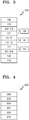
- FIG. 1 is a schematic view of an organic light-emitting device 10 according to an embodiment.
- a structure and a manufacturing method of an organic light-emitting device according to an example of the present disclosure will be described with reference to FIG. 1 .
- the organic light-emitting device 10 of FIG. 1 includes a first electrode 11, a second electrode 19 facing the first electrode 11, and an organic layer 10A between the first electrode 11 and the second electrode 19.
- the organic layer 10A includes an emission layer 15, a hole transport region 12 may be located between the first electrode 11 and the emission layer 15, and an electron transport region 17 may be located between the emission layer 15 and the second electrodes 19.
- a substrate may be additionally located under the first electrode 11 or above the second electrode 19.
- the substrate any substrate that is used in organic light-emitting devices available in the art may be used, and the substrate may be a glass substrate or a transparent plastic substrate, each having excellent mechanical strength, thermal stability, transparency, surface smoothness, ease of handling, and water resistance.
- the first electrode 11 may be formed by depositing or sputtering a material for forming the first electrode11 on the substrate.
- the first electrode 11 may be an anode.
- the material for forming the first electrode 11 may be selected from materials with a high work function to facilitate hole injection.
- the first electrode 11 may be a reflective electrode, a semi-transmissive electrode, or a transmissive electrode.
- a material for forming a first electrode may be selected from indium tin oxide (ITO), indium zinc oxide (IZO), tin oxide (SnO 2 ), zinc oxide (ZnO), and any combinations thereof, but embodiments of the present disclosure are not limited thereto.
- a material for forming a first electrode may be selected from magnesium (Mg), silver (Ag), aluminum (Al), aluminum-lithium (Al-Li), calcium (Ca), magnesium-indium (Mg-In), magnesium-silver (Mg-Ag), and any combinations thereof, but embodiments of the present disclosure are not limited thereto.
- the first electrode 11 may have a single-layered structure or a multi-layered structure including two or more layers.
- the emission layer 15 may include a host, a cooling dopant, and a sensitizer.
- the emission layer may emit fluorescent light. That is, the cooling dopant may be a material that may emit fluorescent light.
- the emission layer 15, which emits the fluorescent light, is clearly distinguished from an emission layer of the related art that emits phosphorescent light.
- the emission layer may include a host, a cooling dopant, and a sensitizer, the cooling dopant and the sensitizer satisfy Conditions 1 and 2, and the sensitizer may include Pt: T decay CD ⁇ T decay S T decay CD ⁇ 1.5 ⁇ s wherein, in Conditions 1 and 2,
- the decay time of the cooling dopant is calculated from a time-resolved photoluminescence spectrum (TRPL) at room temperature with respect to a 40 nm-thickness film (hereinafter referred to as "Film (CD)") obtained by vacuum-codepositing the host and the dopant comprised in the emission layer at the weight ratio of 90:10 on a quartz substrate at the vacuum degree of 10 -7 torr.
- TRPL time-resolved photoluminescence spectrum
- CD 40 nm-thickness film
- the decay time of the sensitizer is calculated from TRPL at room temperature with respect to a 40 nm-thickness film (hereinafter referred to as "Film (S)") obtained by vacuum-codepositing the host and the sensitizer comprised in the emission layer at the weight ratio of 90:10 on a quartz substrate at the vacuum degree of 10 -7 torr.
- the cooling dopant is used to reduce the time during which the triplet excitons of the sensitizer remains in the excited state. Accordingly, an organic light-emitting device including the cooling dopant may have a prolonged lifespan.
- the more triplet excitons the sensitizer has the more excess energy is accumulated in the sensitizer, resulting in more hot excitons. That is, the amount of triplet excitons of the sensitizer is proportional to the amount of hot excitons.
- the hot excitons break down various chemical bonds of a compound included in an emission layer and/or a compound existing at the interface of the emission layer and other layers to degrade the compound. Accordingly, the lifespan of organic light-emitting devices may be reduced.
- the triplet excitons of the sensitizer can be quickly converted to singlet excitons of the cooling dopant, ultimately reducing the amount of hot excitons and increasing the lifespan of an organic light-emitting device.
- hot excitons may be generated or increased by exciton-exciton annihilation due to an increase in the density of excitons in an emission layer, exciton-charge annihilation due to the charge imbalance in an emission layer, and/or radical ion pairs due to the delivery of electrons between a host and dopant.
- Condition 1 In order to quickly convert triplet excitons of the sensitizer to singlet excitons of the cooling dopant, Condition 1 should be satisfied.
- the cooling dopant emits fluorescent light
- a high color purity organic light-emitting device can be provided, and in particular, since Condition 2 is satisfied, so that the singlet excitons of the cooling dopant excited state at room temperature can be rapidly transferred, and thus, the single state of the cooling dopant in the excited state may not be accumulated, and the lifespan of an organic light-emitting device may be increased.
- the organic light-emitting device may further satisfy Condition 4: BDE S ⁇ T 1 S ⁇ 3.0 eV wherein, in Condition 4,
- the organic light-emitting device may have the target level of lifespan by satisfying Condition 5 below: R Hex / e 10 ⁇ 15 wherein, in Condition 5, R (Hex) is the production rate of hot excitons.
- R (Hex) was subjected to the photochemical stability of the organic light-emitting device (photochemical stability), and then calculated through the Gaussian 09 program according to Equation C below.
- R Hex a ⁇ T decay S ⁇ e ⁇ BDE S ⁇ T 1 S wherein, in Equation C,
- the hot-exciton production rate is estimated to be proportional to (decay time) ⁇ e- (BDE-T1) , and in order to obtain the target level of the lifespan of the organic light-emitting device, (hot-exciton production rate)/e 10 should be less than 15.
- PCS degradation analysis
- Singlet and triplet excitons are formed at the host in the emission layer, and the singlet and triplet excitons formed at the host are transferred to the sensitizer and then to the cooling dopant through Forster energy transfer (FRET).
- FRET Forster energy transfer
- an organic light-emitting device type I
- the sensitizer is a thermally activated delayed fluorescence (TADF) emitter satisfying the condition of ⁇ E ST ⁇ 0.3 eV.
- TADF thermally activated delayed fluorescence
- the singlet excitons formed at the host which is 25% of the total excitons, are transferred to the sensitizer through FRET, and the energy of triplet excitons formed at the host, which is 75% of the total excitons, is transferred to the singlet and triplet of the sensitizer, among which the energy delivered to triplet is subjected to RISC into singlet, and then, the singlet energy of the sensitizer is transferred to the cooling dopant through FRET.
- the sensitizer is an organic metallic compound including Pt.
- the triplet excitons formed at the host which is 75% of the total excitons, are transferred to the sensitizer through Dexter energy transfer, and the energy of singlet excitons formed at the host, which is 25% of the total excitons, is transferred to the singlet and triplet of the sensitizer, among which the energy delivered to singlet is subjected to ISC into triplet, and then, the triplet energy of the sensitizer is transferred to the cooling dopant through FRET.
- an organic light-emitting device having improved efficiency can be obtained.
- an organic light-emitting device can be obtained with significantly reduced energy loss, the lifespan characteristics of the organic light-emitting device can be improved.
- the amount of the sensitizer in the emission layer may be from about 5 wt% to about 50 wt%. Within these ranges, it is possible to achieve effective energy transfer in the emission layer, and accordingly, an organic light-emitting device having high efficiency and long lifespan can be obtained.
- the host, the cooling dopant, and the sensitizer may further satisfy Condition 6: T 1 H ⁇ T 1 S ⁇ S 1 CD wherein, in Condition 6,
- the emission layer may consist of the host, the cooling dopant, and the sensitizer. That is, the emission layer may not further include materials other than the host, the cooling dopant, and the sensitizer.
- a thickness of the emission layer may be in a range of about 100 ⁇ to about 1,000 ⁇ , for example, about 200 ⁇ to about 600 ⁇ . When the thickness of the emission layer is within this range, excellent light-emission characteristics may be obtained without a substantial increase in driving voltage.
- the host may include no metal atoms.
- the host may include one kind of host.
- the one host may be selected from an amphiprotic host, an electron transport host, and a hole transport host, which will be described later.
- the host may include a mixture of two or more different hosts.
- the host may be a mixture of an electron transport host and a hole transport host, a mixture of two types of electron transport hosts different from each other, or a mixture of two types of hole transport hosts different from each other.
- the electron transport host and the hole transport host may be understood by referring to the related description to be presented later.
- the host may include an electron transport host including at least one electron transport moiety and a hole transport host that is free of an electron transport moiety.
- the electron transport moiety used herein may be selected from a cyano group, a ⁇ electron-deficient nitrogen-containing cyclic group, and a group represented by one of the following Formulae:
- ⁇ , ⁇ ', and ⁇ " are each binding sites to neighboring atoms.
- the electron transport host of the emission layer 15 may include at least one of a cyano group and a ⁇ electron-deficient nitrogen-containing cyclic group.
- the electron transport host in the emission layer 15 may include at least one cyano group.
- the electron transport host in the emission layer 15 may include at least one cyano group and at least one ⁇ electron deficient nitrogen-containing cyclic group.
- the host may include an electron transport host and a hole transport host, wherein the electron transport host may include at least one ⁇ electron-deficient nitrogen-free cyclic group and at least one electron transport moiety, and the hole transport host may include at least one ⁇ electron-deficient nitrogen-free cyclic group and may not include an electron transport moiety.
- the ⁇ electron-deficient nitrogen-free cyclic group may be selected from a benzene group, a heptalene group, an indene group, a naphthalene group, an azulene group, an indacene group, acenaphthylene group, a fluorene group, a spiro-bifluorene group, a benzofluorene group, a dibenzofluorene group, a phenalene group, a phenanthrene group, an anthracene group, a fluoranthene group, a triphenylene group, a pyrene group, a chrysene group, a naphthacene group, a picene group, a perylene group, a pentacene group, a hexacene group, a pentaphene group, a rubicene group, a coronene group, an ovalene
- the electron transport host may be selected from compounds represented by Formula E-1, and the hole transport host may be selected from compounds represented by Formula H-1, but embodiments of the present disclosure are not limited thereto: ⁇ Formula E-1> [Ar 301 ] xb11 -[(L 301 ) xb1 -R 301 ] xb21 wherein, in Formula E-1,
- Ar 301 and L 301 in Formula E-1 may each independently be selected from a benzene group, a naphthalene group, a fluorene group, a spiro-bifluorene group, a benzofluorene group, a dibenzofluorene group, a phenalene group, a phenanthrene group, an anthracene group, a fluoranthene group, a triphenylene group, a pyrene group, a chrysene group, a naphthacene group, a picene group, a perylene group, a pentaphene group, an indenoanthracene group, a dibenzofuran group, a dibenzothiophene group, an imidazole group, a pyrazole group, a thiazole group, an isothiazole group, an oxazole group, an isoxazole group, an isox
- Ar 301 may be selected from a benzene group, a naphthalene group, a fluorene group, a spiro-bifluorene group, a benzofluorene group, a dibenzofluorene group, a phenalene group, a phenanthrene group, an anthracene group, a fluoranthene group, a triphenylene group, a pyrene group, a chrysene group, a naphthacene group, a picene group, a perylene group, a pentaphene group, an indenoanthracene group, a dibenzofuran group, and a dibenzothiophene group, each unsubstituted or substituted with at least one selected from deuterium, -F, -CI, -Br, -I, a hydroxyl group, a cyano group, a
- L 301 may be selected from groups represented by Formulae 5-2, 5-3 and 6-8 to 6-33.
- R 301 may be selected from a cyano group and groups represented by Formula 7-1 to 7-18, and at least one of Ar 402 (s) in the number of xd11 may be selected from groups represented by Formulae 7-1 to 7-18, but embodiments of the present disclosure are not limited thereto: wherein, in Formulae 7-1 to 7-18, xb41 to xb44 may each be 0, 1, or 2, wherein xb41 in Formula 7-10 is not 0, the sum of xb41 and xb42 in Formulae 7-11 to 7-13 is not 0, the sum of xb41, xb42, and xb43 in Formulae 7-14 to 7-16 is not 0, the sum of xb41, xb42, xb43, and xb44 in Formulae 7-17 and 7-18 is not 0, and ⁇ indicates a binding site to a neighboring atom.
- Two or more Ar 301 (s) in Formula E-1 may be identical to or different from each other, two or more L 301 (s) may be identical to or different from each other, two or more L 401 (S) in Formula H-1 may be identical to or different from each other, and two or more Ar 402 (s) in Formula H-1 may be identical to or different from each other.
- the electron transport host includes i) at least one of a cyano group, a pyrimidine group, a pyrazine group, and a triazine group and ii) a triphenylene group, and the hole transport host may include a carbazole group.
- the electron transport host may include at least one cyano group.
- the electron transport host may be, for example, selected from groups HE1 to HE7, but embodiments of the present disclosure are not limited thereto:
- the hole transport host may be selected from Compounds H-H1 to H-H103, but embodiments of the present disclosure are not limited thereto:
- the amphiprotic host may be selected from group HEH1, but embodiments of the present disclosure are not limited thereto: ⁇ group HEH1> wherein, in Compounds 1 to 432, Ph may be a phenyl group.
- the weight ratio of the electron transport host and hole transport host may be 1: 9 to 9: 1, for example, 2: 8 to 8: 2, for example, 4: 6 to 6: 4, for example, 5: 5.
- the weight ratio of the electron transport host and the hole transport host satisfies the above-described ranges, the hole-and-electron transport balance in the emission layer 15 may be made.
- organic light-emitting devices Since the cooling dopant emits fluorescent light, organic light-emitting devices according to an embodiment of the present disclosure are clearly distinguished from organic light-emitting devices containing compounds that emit phosphorescent light.
- the cooling dopant satisfies Condition 2, as described above.
- the maximum emission wavelength of the emission spectrum of the cooling dopant may be 400 nm or more and 550 nm or less.
- the maximum emission wavelength of the emission spectrum of the cooling dopant may be 400 nm or more and 495 nm or less, or 450 nm or more and 495 nm or less, but embodiments of the present disclosure are not limited thereto.
- the cooling dopant may emit blue light.
- the "maximum emission wavelength” refers to a wavelength at which the emission intensity is the greatest, and may also be referred to as "a peak emission wavelength".
- the cooling dopant may not include metal atoms.
- the cooling dopant may be selected from a condensed polycyclic compound and a styryl-based compound.
- the cooling dopant may include one of a naphthalene-containing core, a fluorene-containing core, a spiro-bifluorene-containing core, a benzofluorene-containing core, a dibenzofluorene-containing core, a phenanthrene-containing core, an anthracene-containing core, a fluoranthene-containing core, a triphenylene-containing core, a pyrene-containing core, a chrysene-containing core, a naphthacene-containing core, a picene-containing core, a perylene-containing core, a pentaphene-containing core, an indenoanthracene-containing core, a bisanthracene-containing core, and cores represented by Formulae 501-1 to 501-18, but embodiments of the present disclosure are not limited thereto:
- the cooling dopant may be selected from a styryl-amine-based compound and a styryl-carbazole-based compound, but embodiments of the present disclosure are not limited thereto.
- the cooling dopant may be selected from compounds represented by Formula 501:
- Ar 501 may be selected from:
- Ar 501 may be selected from:
- the cooling dopant may include a compound represented by one of Formulae 502-1 to 502-5: wherein, in Formulae 502-1 to 502-5,
- the cooling dopant may include at least one compound selected from, for example, the following compounds FD(1) to FD(16) and FD1 to FD18:
- the amount of the cooling dopant in the emission layer may be from about 0.01 wt% to about 15 wt%, but embodiments of the present disclosure are not limited thereto.
- the sensitizer may include Pt.
- the sensitizer may be an organic metallic compound containing Pt.
- the sensitizer may include Pt and an organic ligand (L 11 ), and L 11 and Pt may form 1, 2, 3, or 4 cyclometalated rings.
- the sensitizer may include an organometallic compound represented by Formula 101: ⁇ Formula 101> Pt(L 11 ) n11 (L 12 ) n12 wherein, in Formula 101,
- the sensitizer may be selected from Groups I, II, III, V and VI, but embodiments of the present disclosure are not limited thereto: ⁇ Group I> ⁇ Group II> ⁇ Group III> ⁇ group V> a compound represented by Formula A below: ⁇ Formula A> (L 101 ) n101 -M 101 -(L 102 ) m101 L 101 , n101, M 101 , L 102 , and m101 in Formula A are the same as shown in Table 1: Table 1 Compound name L 101 n101 M 101 L 102 m101 BD263 LM11 2 Pt - 0 BD264 LM13 2 Pt - 0 BD265 LM15 2 Pt - 0 BD266 LM45 2 Pt - 0 BD267 LM47 2 Pt - 0 BD268 LM49 2 Pt - 0 BD269 LM98 2 Pt - 0 BD270 LM100 2 P
- the sensitizer may be a thermally activated delayed fluorescence emitter.
- Thermally activated delayed fluorescence emitter may not include metal.
- thermally activated delayed fluorescence emitter may satisfy Condition 7: ⁇ E ST ⁇ 0.3 eV wherein, in Condition 7, ⁇ E ST is the difference between the lowest excitation singlet energy level and the lowest excitation triplet energy level of the sensitizer.
- the sensitizer may include thermally activated delayed fluorescence emitter represented by Formula 201 or 202: In Formulae 201 and 202,
- a 21 in Formula 201 and 202 may be a substituted or unsubstituted ⁇ electron-deficient nitrogen-free cyclic group.
- the ⁇ electron-deficient nitrogen-free cyclic group may be selected from a benzene group, a heptalene group, an indene group, a naphthalene group, an azulene group, an indacene group, acenaphthylene group, a fluorene group, a spiro-bifluorene group, a benzofluorene group, a dibenzofluorene group, a phenalene group, a phenanthrene group, an anthracene group, a fluoranthene group, a triphenylene group, a pyrene group, a chrysene group, a naphthacene group, a picene group, a perylene group, a pentacene group, a hexacene group, a pentaphene group, a rubicene group, a coronene group, an oval
- D 21 in Formulae 201 and 202 may be selected from: -F, a cyano group, and an ⁇ -electron deficient nitrogen-containing cyclic group; a C 1 -C 60 alkyl group, a ⁇ -electron deficient nitrogen-containing cyclic group, and a ⁇ electron-deficient nitrogen-free cyclic group, each substituted with at least one selected from -F and a cyano group; and a ⁇ -electron deficient nitrogen-containing cyclic group, each substituted with at least one selected from deuterium, a C 1 -C 60 alkyl group, an ⁇ -electron deficient nitrogen-containing cyclic group, and an ⁇ electron-deficient nitrogen-free cyclic group.
- the ⁇ electron-deficient nitrogen-free cyclic group is the same as described above.
- the sensitizer may be selected from Groups VII to XI, but embodiments of the present disclosure are not limited thereto:
- the hole transport region 12 may be located between the first electrode 11 and the emission layer 15 of the organic light-emitting device 10.
- the hole transport region 12 may have a single-layered structure or a multi-layered structure.
- the hole transport region 12 may have a hole injection layer, a hole transport layer, a hole injection layer/hole transport layer structure, a hole injection layer/first hole transport layer/second hole transport layer structure, a hole transport layer/middle layer structure, a hole injection layer/hole transport layer/middle layer structure, a hole transport layer/electron blocking layer or hole injection layer/hole transport layer/electron blocking layer structure, but embodiments of the present disclosure are not limited thereto.
- the hole transport region 12 may include any compound having hole transport properties.
- the hole transport region 12 may include an amine-based compound.
- the hole transport region 1 may include at least one selected from a compound represented by Formula 201 to a compound represented by Formula 205, but embodiments of the present disclosure are not limited thereto: wherein, in Formulae 201 to 205,
- L 201 to L 209 may be selected from a benzene group, a heptalene group, an indene group, a naphthalene group, an azulene group, a heptalene group, an indacene group, an acenaphthylene group, a fluorene group, a spiro-bifluorene group, a benzofluorene group, a dibenzofluorene group, a phenalene group, a phenanthrene group, an anthracene group, a fluoranthene group, a triphenylene group, a pyrene group, a chrysene group, a naphthacene group, a picene group, a perylene group, a pentacene group, a hexacene group, a pentaphene group, a rubicene group, a coronene group, a
- the hole transport region 12 may include a carbazole-containing amine-based compound.
- the hole transport region 12 may include a carbazole-containing amine-based compound and a carbazole-free amine-based compound.
- the carbazole-containing amine-based compound may be selected from, for example, compounds represented by Formula 201 including a carbazole group and further including at least one selected from a dibenzofuran group, a dibenzothiophene group, a fluorene group, a spiro-bifluorene group, an indenocarbazole group, an indolocarbazole group, a benzofurocarbazole group, and a benzothienocarbazole group.
- Formula 201 including a carbazole group and further including at least one selected from a dibenzofuran group, a dibenzothiophene group, a fluorene group, a spiro-bifluorene group, an indenocarbazole group, an indolocarbazole group, a benzofurocarbazole group, and a benzothienocarbazole group.
- the carbazole-free amine-based compound may be selected from, for example, compounds represented by Formula 201 which do not include a carbazole group and which include at least one selected from a dibenzofuran group, a dibenzothiophene group, a fluorene group, a spiro-bifluorene group, an indenocarbazole group, an indolocarbazole group, a benzofurocarbazole group, and a benzothienocarbazole group.
- Formula 201 which do not include a carbazole group and which include at least one selected from a dibenzofuran group, a dibenzothiophene group, a fluorene group, a spiro-bifluorene group, an indenocarbazole group, an indolocarbazole group, a benzofurocarbazole group, and a benzothienocarbazole group.
- the hole transport region 12 may include at least one selected from compounds represented by Formulae 201 or 202.
- the hole transport region 12 may include at least one selected from compounds represented by Formulae 201-1, 202-1 and 201-2, but embodiments of the present disclosure are not limited thereto:
- R 201 and R 202 are the same as described herein, and R 211 to R 213 are each independently selected from hydrogen, deuterium, -F, -Cl, -Br, -I, a hydroxyl group, a cyano group, a nitro group, an amidino group, a hydrazine group, a hydrazone group, a C 1 -C 20 alkyl group, a C 1 -C 20 alkoxy group, a phenyl group, a biphenyl group, a terphenyl group, a phenyl group substituted with a C 1 -C 10 alkyl group, a phenyl group substituted with -F, a naphthyl group, a fluorenyl group, a spiro-bifluoreny
- the hole transport region 12 may include at least one selected from Compounds HT1 to HT39, but embodiments of the present disclosure are not limited thereto.
- hole transport region 12 of the organic light-emitting device 10 may further include a p-dopant.
- the hole transport region 12 may have a matrix (for example, at least one of compounds represented by Formulae 201 to 205) and a p-dopant included in the matrix.
- the p-dopant may be uniformly or non-uniformly doped in the hole transport region 12.
- the LUMO energy level of the p-dopant may be -3.5 eV or less.
- the p-dopant may include at least one selected from a quinone derivative, a metal oxide, and a cyano-containing compound, but embodiments of the present disclosure are not limited thereto.
- the p-dopant may include at least one selected from:
- R 221 to R 223 may each independently be selected from a substituted or unsubstituted C 3 -C 10 cycloalkyl group, a substituted or unsubstituted C 1 -C 10 heterocycloalkyl group, a substituted or unsubstituted C 3 -C 10 cycloalkenyl group, a substituted or unsubstituted C 1 -C 10 heterocycloalkenyl group, a substituted or unsubstituted C 6 -C 60 aryl group, a substituted or unsubstituted C 1 -C 60 heteroaryl group, a substituted or unsubstituted monovalent non-aromatic condensed polycyclic group, and a substituted or unsubstituted monovalent non-aromatic condensed heteropolycyclic group, and at least one selected from R 221 to R 223 may have at least one substituent selected from a cyano group, -F, -Cl
- the hole transport region 12 may have a thickness of about 100 ⁇ to about 10000 ⁇ , for example, about 400 ⁇ to about 2000 ⁇ , and the emission layer 15 may have a thickness of about 100 ⁇ to about 3000 ⁇ , for example, about 300 ⁇ to about 1000 ⁇ .
- the thickness of each of the hole transport region 12 and the emission layer 15 is within these ranges described above, satisfactory hole transportation characteristics and/or luminescent characteristics may be obtained without a substantial increase in driving voltage.
- the electron transport region 17 is placed between the emission layer 15 and the second electrode 19 of the organic light-emitting device 10.
- the electron transport region 17 may have a single-layered structure or a multi-layered structure.
- the electron transport region 17 may have an electron transport layer, an electron transport layer/electron injection layer structure, a buffer layer/electron transport layer structure, hole blocking layer/electron transport layer structure, a buffer layer/electron transport layer/electron injection layer structure, or a hole blocking layer/electron transport layer/electron injection layer structure, but embodiments of the present disclosure are not limited thereto.
- the electron transport region 17 may further include an electron control layer.
- the electron transport region 17 may include known electron transport materials.
- the electron transport region (for example, a buffer layer, a hole blocking layer, an electron control layer, or an electron transport layer in the electron transport region) may include a metal-free compound containing at least one ⁇ electron-deficient nitrogen-containing cyclic group.
- the ⁇ electron-deficient nitrogen-containing cyclic group is the same as described above.
- the electron transport region may include a compound represented by Formula 601 below: ⁇ Formula 601> [Ar 601 ] xe11 -[(L 601 ) xe1 -R 601 ] xe21
- Ar 601 and L 601 may each independently be a substituted or unsubstituted C 5 -C 60 carbocyclic group or a substituted or unsubstituted C 1 -C 60 heterocyclic group
- xe11 may be 1, 2, or 3
- xe1 may be an integer from 0 to 5
- R 601 may be selected from a substituted or unsubstituted C 3 -C 10 cycloalkyl group, a substituted or unsubstituted C 1 -C 10 heterocycloalkyl group, a substituted or unsubstituted C 3 -C 10 cycloalkenyl group, a substituted or unsubstituted C 1 -C 10 heterocycloalkenyl group, a substituted or unsubstituted C 6 -C 60 aryl group, a substituted or unsubstituted C 6 -C 60 aryloxy group, a substituted or unsubstituted C 6 -C
- At least one of Ar 601 (s) in the number of xe11 and R 601 (s) in the number of xe21 may include the ⁇ electron-deficient nitrogen-containing cyclic group.
- ring Ar 601 and L 601 in Formula 601 may each independently be selected from a benzene group, a naphthalene group, a fluorene group, a spiro-bifluorene group, a benzofluorene group, a dibenzofluorene group, a phenalene group, a phenanthrene group, an anthracene group, a fluoranthene group, a triphenylene group, a pyrene group, a chrysene group, a naphthacene group, a picene group, a perylene group, a pentaphene group, an indenoanthracene group, a dibenzofuran group, a dibenzothiophene group, a carbazole group, an imidazole group, a pyrazole group, a thiazole group, an isothiazole group, an oxazole group,
- xe11 in Formula 601 is 2 or more, two or more Ar 601 (s) may be linked to each other via a single bond.
- Ar 601 in Formula 601 may be an anthracene group.
- the compound represented by Formula 601 may be represented by Formula 601-1:
- X 614 may be N or C(R 614 ), X 615 may be N or C(R 615 ), X 616 may be N or C(R 616 ), and at least one selected from X 614 to X 616 may be N, L 611 to L 613 may each independently be the same as described in connection with L 601 , xe611 to xe613 may each independently be the same as described in connection with xe1, R 611 to R 613 may each independently be the same as described in connection with R 601 , and R 614 to R 616 may each independently be selected from hydrogen, deuterium, -F, -Cl, -Br, -I, a hydroxyl group, a cyano group, a nitro group, an amidino group, a hydrazino group, a hydrazono group, a C 1 -C 20 alkyl group, a C 1 -C 20 alkoxy group, a pheny
- xe1 and xe611 to xe613 in Formulae 601 and 601-1 may each independently be 0, 1, or 2.
- R 601 and R 611 to R 613 in Formulae 601 and 601-1 may each independently be selected from a phenyl group, a biphenyl group, a terphenyl group, a naphthyl group, a fluorenyl group, a spiro-bifluorenyl group, a benzofluorenyl group, a dibenzofluorenyl group, a phenanthrenyl group, an anthracenyl group, a fluoranthenyl group, a triphenylenyl group, a pyrenyl group, a chrysenyl group, a perylenyl group, a pentaphenyl group, a hexacenyl group, a pentacenyl group, a thiophenyl group, a furanyl group, a carbazolyl group, an indolyl group, an isoindoly
- the electron transport region may include at least one compound selected from Compounds ET1 to ET36, but embodiments of the present disclosure are not limited thereto:
- the electron transport region may include at least one selected from 2,9-dimethyl-4,7-diphenyl-1,10-phenanthroline (BCP), 4,7-dphenyl-1,10-phenanthroline (Bphen), Alq 3 , BAlq, 3-(biphenyl-4-yl)-5-(4-tert-butylphenyl)-4-phenyl-4H-1,2,4-triazole (TAZ), and NTAZ:
- Thicknesses of the buffer layer, the hole blocking layer, and the electron control layer may each independently be in a range of about 20 ⁇ to about 1,000 ⁇ , for example, about 30 ⁇ to about 300 ⁇ . When the thicknesses of the buffer layer, the hole blocking layer, and the electron control layer are within these ranges, excellent hole blocking characteristics or excellent electron control characteristics may be obtained without a substantial increase in driving voltage.
- a thickness of the electron transport layer may be in a range of about 100 ⁇ to about 1,000 ⁇ , for example, about 150 ⁇ to about 500 ⁇ . When the thickness of the electron transport layer is within the range described above, the electron transport layer may have satisfactory electron transport characteristics without a substantial increase in driving voltage.
- the electron transport region 17 may further include, in addition to the materials described above, a metal-containing material.
- the metal-containing material may include at least one selected from alkali metal complex and alkaline earth-metal complex.
- the alkali metal complex may include a metal ion selected from a Li ion, a Na ion, a K ion, a Rb ion, and a Cs ion
- the alkaline earth-metal complex may include a metal ion selected from a Be ion, a Mg ion, a Ca ion, a Sr ion, and a Ba ion.
- a ligand coordinated with the metal ion of the alkali metal complex or the alkaline earth-metal complex may be selected from a hydroxy quinoline, a hydroxy isoquinoline, a hydroxy benzoquinoline, a hydroxy acridine, a hydroxy phenanthridine, a hydroxy phenyloxazole, a hydroxy phenylthiazole, a hydroxy diphenyloxadiazole, a hydroxy diphenylthiadiazole, a hydroxy phenylpyridine, a hydroxy phenylbenzimidazole, a hydroxy phenylbenzothiazole, a bipyridine, a phenanthroline, and a cyclopentadiene, but embodiments of the present disclosure are not limited thereto.
- the metal-containing material may include a Li complex.
- the Li complex may include, for example, Compound ET-D1 (lithium quinolate, LiQ) or ET-D2:
- the electron transport region 17 may include an electron injection layer that facilitates injection of electrons from the second electrode 19.
- the electron injection layer may directly contact the second electrode 19.
- the electron injection layer may have i) a single-layered structure including a single layer including a single material, ii) a single-layered structure including a single layer including a plurality of different materials, or iii) a multi-layered structure having a plurality of layers including a plurality of different materials.
- the electron injection layer may include an alkali metal, an alkaline earth metal, a rare earth metal, an alkali metal compound, an alkaline earth-metal compound, a rare earth metal compound, an alkali metal complex, an alkaline earth-metal complex, a rare earth metal complex, or any combinations thereof.
- the alkali metal may be selected from Li, Na, K, Rb, and Cs. In one embodiment, the alkali metal may be Li, Na, or Cs. In one or more embodiments, the alkali metal may be Li or Cs, but embodiments of the present disclosure are not limited thereto.
- the alkaline earth metal may be selected from Mg, Ca, Sr, and Ba.
- the rare earth metal may be selected from Sc, Y, Ce, Tb, Yb, and Gd.
- the alkali metal compound, the alkaline earth-metal compound, and the rare earth metal compound may be selected from oxides and halides (for example, fluorides, chlorides, bromides, or iodides) of the alkali metal, the alkaline earth-metal, and the rare earth metal.
- oxides and halides for example, fluorides, chlorides, bromides, or iodides
- the alkali metal compound may be selected from alkali metal oxides, such as Li 2 O, Cs 2 O, or K 2 O, and alkali metal halides, such as LiF, NaF, CsF, KF, LiI NaI, CsI or KI
- alkali metal compound may be selected from LiF, Li 2 O, NaF, LiI NaI CsI and KI but embodiments of the present disclosure are not limited thereto.
- the alkaline earth-metal compound may be selected from alkaline earth-metal oxides, such as BaO, SrO, CaO, Ba x Sr 1-x O (0 ⁇ x ⁇ 1), or Ba x Ca 1-x O (0 ⁇ x ⁇ 1).
- the alkaline earth-metal compound may be selected from BaO, SrO, and CaO, but embodiments of the present disclosure are not limited thereto.
- the rare earth metal compound may be selected from YbF 3 , ScF 3 , ScO 3 , SC 2 O3, Y 2 O3, Ce 2 O 3 , GdF 3 , and TbF 3 .
- the rare earth metal compound may be selected from YbF 3 , ScF 3 , TbF 3 , YbI 3 , ScI 3 , and TbI 3 , but embodiments of the present disclosure are not limited thereto.
- the alkali metal complex, the alkaline earth-metal complex, and the rare earth metal complex may include an ion of alkali metal, alkaline earth-metal, and rare earth metal as described above, and a ligand coordinated with a metal ion of the alkali metal complex, the alkaline earth-metal complex, or the rare earth metal complex may be selected from hydroxy quinoline, hydroxy isoquinoline, hydroxy benzoquinoline, hydroxy acridine, hydroxy phenanthridine, hydroxy phenyloxazole, hydroxy phenylthiazole, hydroxy diphenyloxadiazole, hydroxy diphenylthiadiazole, hydroxy phenylpyridine, hydroxy phenylbenzimidazole, hydroxy phenylbenzothiazole, bipyridine, phenanthroline, and cyclopentadiene, but embodiments of the present disclosure are not limited thereto.
- the electron injection layer may consist of an alkali metal, an alkaline earth metal, a rare earth metal, an alkali metal compound, an alkaline earth-metal compound, a rare earth metal compound, an alkali metal complex, an alkaline earth-metal complex, a rare earth metal complex, or any combinations thereof, as described above.
- the electron injection layer may further include an organic material.
- an alkali metal, an alkaline earth metal, a rare earth metal, an alkali metal compound, an alkaline earth-metal compound, a rare earth metal compound, an alkali metal complex, an alkaline earth-metal complex, a rare earth metal complex, or any combinations thereof may be homogeneously or non-homogeneously dispersed in a matrix including the organic material.
- a thickness of the electron injection layer may be in a range of about 1 ⁇ to about 100 ⁇ , for example, about 3 ⁇ to about 90 ⁇ . When the thickness of the electron injection layer is within the range described above, the electron injection layer may have satisfactory electron injection characteristics without a substantial increase in driving voltage.
- the second electrode 19 is located on the organic layer 10A having such a structure.
- the second electrode 19 may be a cathode which is an electron injection electrode, and in this regard, a material for forming the second electrode 19 may be selected from a metal, an alloy, an electrically conductive compound, and a combination thereof, which have a relatively low work function.
- the second electrode 19 may include at least one selected from lithium (Li), silver (Ag), magnesium (Mg), aluminum (Al), aluminum-lithium (Al-Li), calcium (Ca), magnesium-indium (Mg-In), magnesium-silver (Mg-Ag), ITO, and IZO, but embodiments of the present disclosure are not limited thereto.
- the second electrode 19 may be a transmissive electrode, a semi-transmissive electrode, or a reflective electrode.
- the second electrode 19 may have a single-layered structure having a single layer or a multi-layered structure including two or more layers.
- FIG. 3 is a schematic cross-sectional view of an organic light-emitting device 100 according to another embodiment.
- the organic light-emitting device 100 of FIG. 3 includes a first electrode 110, a second electrode 190 facing the first electrode 110, and a first emission unit 151 and a second emission unit 152 between the first electrode 110 and the second electrode 190.
- a charge generating layer 141 is located between the first emission unit 151 and the second emission unit 152, and the charge generating layer 141 may include an n-type charge generating layer 141-N and a p-type charge generating layer 141-P.
- the charge generating layer 141 is a layer that generates charge and supplies the charge to neighboring emission units, and any known material may be used therefor.
- the first emission unit 151 may include a first emission layer 151-EM
- the second emission unit 152 may include a second emission layer 152-EM.
- the maximum emission wavelength of light emitted from the first emission unit 151 may be different from the maximum emission wavelength of light emitted from the second emission unit 152.
- the mixed light of the light emitted from the first emission unit 151 and the light emitted from the second emission unit 152 may be white light, but embodiments of the present disclosure are not limited thereto.
- the hole transport region 120 is located between the first emission unit 151 and the first electrode 110, and the second emission unit 152 may include the first hole transport region 121 located on the side of the first electrode 110 .
- An electron transport region 170 is located between the second emission unit 152 and the second electrode 190, and the first emission unit 151 may include a first electron transport region 171 located between the charge generating layer 141 and the first emission layer 151-EM.
- the first emission layer 151-EM may include a host, a cooling dopant, and a sensitizer, and the cooling dopant and the sensitizer may satisfy Conditions 1 and 2.
- the second emission layer 152-EM may include a host, a cooling dopant, and a sensitizer, and the cooling dopant and the sensitizer may satisfy Conditions 1 and 2.
- the first electrode 110 and the second electrode 190 illustrated in FIG. 3 may be the same as described in connection with the first electrode 11 and the second electrode 19 illustrated in FIG. 1 .
- the first emission layer 151-EM and the second emission layer 152-EM illustrated in FIG. 3 are each the same as described in connection with the emission layer 15 illustrated in FIG. 1 .
- the hole transport region 120 and the first hole transport region 121 illustrated in FIG. 3 are each the same as described in connection with the hole transport region 12 illustrated in FIG. 1 .
- the electron transport region 170 and the first electron transport region 171 illustrated in FIG. 3 are each the same as described in connection with the electron transport region 17 illustrated in FIG. 1 .
- each of the first emission unit 151 and the second emission unit 152 includes an emission layer including a host, a cooling dopant, and a sensitizer.
- the organic light-emitting device may have various other forms.
- one of the first emission unit 151 and the second emission unit 152 of the organic light-emitting device 100 of FIG. 3 may be replaced with any known emission unit, or may include three or more emission units.
- FIG. 4 is a schematic cross-sectional view of an organic light-emitting device 200 according to another embodiment.
- the organic light-emitting device 200 includes a first electrode 210, a second electrode 290 facing the first electrode 210, and a first emission layer 251 and a second emission layer 252 which are stacked between the first electrode 210 and the second electrode 290.
- the maximum emission wavelength of light emitted from the first emission layer 251 may be different from the maximum emission wavelength of light emitted from the second emission layer 252.
- the mixed light of the light emitted from the first emission layer 251 and the light emitted from the second emission layer 252 may be white light, but embodiments of the present disclosure are not limited thereto.
- a hole transport region 220 may be located between the first emission layer 251 and the first electrode 210, and an electron transport region 270 may be located between the second emission layer 252 and the second electrode 290.
- the first emission layer 251 may include a host, a cooling dopant, and a sensitizer, and the cooling dopant and the sensitizer may satisfy Conditions 1 and 2.
- the second emission layer 252 may include a host, a cooling dopant, and a sensitizer, and the cooling dopant and the sensitizer may satisfy Conditions 1 and 2.
- the first electrode 210, the hole transport region 220, and the second electrode 290 illustrated in FIG. 4 are respectively the same as described in connection with the first electrode 11, the hole transport region 12, and the second electrode 19 illustrated in FIG. 1 .
- the first emission layer 251 and the second emission layer 252 illustrated in FIG. 4 are each the same as described in connection with the emission layer 15 illustrated in FIG. 1 .
- the electron transport region 270 illustrated in FIG. 4 may be the same as described in connection with the electron transport region 17 in FIG. 1 .
- each of the first emission layer 251 and the second emission layer 252 includes a host, a cooling dopant, and a sensitizer.
- the organic light-emitting device may have various other forms.
- one of the first emission layer 251 and the second emission layer 252 of the organic light-emitting device 200 of FIG. 4 may be replaced with any known emission layer, or an interlayer may be additionally located between neighboring emission layers.
- C 1 -C 60 alkyl group refers to a linear or branched saturated aliphatic hydrocarbon monovalent group having 1 to 60 carbon atoms, and examples thereof include a methyl group, an ethyl group, a propyl group, an isobutyl group, a sec-butyl group, a tert-butyl group, a pentyl group, an isoamyl group, and a hexyl group.
- C 1 -C 60 alkylene group refers to a divalent group having the same structure as the C 1 -C 60 alkyl group.
- C 1 -C 60 alkoxy group refers to a monovalent group represented by -OA 101 (wherein A 101 is the C 1 -C 60 alkyl group), and examples thereof include a methoxy group, an ethoxy group, and an isopropyloxy group.
- C 2 -C 60 alkenyl group refers to a hydrocarbon group formed by substituting at least one carbon-carbon double bond in the middle or at the terminus of the C 2 -C 60 alkyl group, and examples thereof include an ethenyl group, a propenyl group, and a butenyl group.
- C 2 -C 60 alkenylene group refers to a divalent group having the same structure as the C 2 -C 60 alkenyl group.
- C 2 -C 60 alkynyl group refers to a hydrocarbon group formed by substituting at least one carbon-carbon triple bond in the middle or at the terminus of the C 2 -C 60 alkyl group, and examples thereof include an ethynyl group, and a propynyl group.
- C 2 -C 60 alkynylene group refers to a divalent group having the same structure as the C 2 -C 60 alkynyl group.
- C 3 -C 10 cycloalkyl group refers to a monovalent saturated hydrocarbon monocyclic group having 3 to 10 carbon atoms, and examples thereof include a cyclopropyl group, a cyclobutyl group, a cyclopentyl group, a cyclohexyl group, and a cycloheptyl group.
- C 3 -C 10 cycloalkylene group refers to a divalent group having the same structure as the C 3 -C 10 cycloalkyl group.
- C 1 -C 10 heterocycloalkyl group refers to a monovalent saturated monocyclic group having at least one heteroatom selected from N, O, P, Si, and S as a ring-forming atom and 1 to 10 carbon atoms, and non-limiting examples thereof include a tetrahydrofuranyl group, and a tetrahydrothiophenyl group.
- C 1 -C 10 heterocycloalkylene group refers to a divalent group having the same structure as the C 1 -C 10 heterocycloalkyl group.
- C 3 -C 10 cycloalkenyl group refers to a monovalent monocyclic group that has 3 to 10 carbon atoms and at least one carbon-carbon double bond in the ring thereof and no aromaticity, and non-limiting examples thereof include a cyclopentenyl group, a cyclohexenyl group, and a cycloheptenyl group.
- C 3 -C 10 cycloalkenylene group refers to a divalent group having the same structure as the C 3 -C 10 cycloalkenyl group.
- C 1 -C 10 heterocycloalkenyl group refers to a monovalent monocyclic group that has at least one heteroatom selected from N, O, P, Si, and S as a ring-forming atom, 1 to 10 carbon atoms, and at least one carbon-carbon double bond in its ring.
- Examples of the C 1 -C 10 heterocycloalkenyl group are a 2,3-dihydrofuranyl group, and a 2,3-dihydrothiophenyl group.
- C 1 -C 10 heterocycloalkenylene group refers to a divalent group having the same structure as the C 1 -C 10 heterocycloalkenyl group.
- C 6 -C 60 aryl group refers to a monovalent group having a carbocyclic aromatic system having 6 to 60 carbon atoms
- C 6 -C 60 arylene group refers to a divalent group having a carbocyclic aromatic system having 6 to 60 carbon atoms.
- Examples of the C 6 -C 60 aryl group include a phenyl group, a naphthyl group, an anthracenyl group, a phenanthrenyl group, a pyrenyl group, and a chrysenyl group.
- the C 6 -C 60 aryl group and the C 6 -C 60 arylene group each include two or more rings, the rings may be fused to each other.
- C 1 -C 60 heteroaryl group refers to a monovalent group having a heterocarbocyclic aromatic system that has at least one heteroatom selected from N, O, P, Si, and S as a ring-forming atom, and 1 to 60 carbon atoms.
- C 1 -C 60 heteroarylene group refers to a divalent group having a carbocyclic aromatic system that has at least one heteroatom selected from N, O, P, and S as a ring-forming atom, and 1 to 60 carbon atoms.
- Examples of the C 1 -C 60 heteroaryl group include a pyridinyl group, a pyrimidinyl group, a pyrazinyl group, a pyridazinyl group, a triazinyl group, a quinolinyl group, and an isoquinolinyl group.
- the C 6 -C 60 heteroaryl group and the C 6 -C 60 heteroarylene group each include two or more rings, the rings may be fused to each other.
- C 6 -C 60 aryloxy group refers to -OA 102 (wherein A 102 is the C 6 -C 60 aryl group), and a C 6 -C 60 arylthio group used herein refers to -SA 103 (wherein A 103 is the C 6 -C 60 aryl group).
- the term "monovalent non-aromatic condensed polycyclic group” used herein refers to a monovalent group in which two or more rings are condensed with each other, only carbon is used as a ring-forming atom (for example, the number of carbon atoms may be 8 to 60) and the whole molecule is a non-aromaticity group.
- Examples of the monovalent non-aromatic condensed polycyclic group include a fluorenyl group.
- divalent non-aromatic condensed polycyclic group as used herein refers to a divalent group having the same structure as the monovalent non-aromatic condensed polycyclic group.
- the term "monovalent non-aromatic condensed heteropolycyclic group” as used herein refers to a monovalent group having two or more rings condensed to each other, a heteroatom selected from N, O, P, Si, and S, other than carbon atoms(for example, having 1 to 60 carbon atoms), as a ring-forming atom, and no aromaticity in its entire molecular structure.
- Examples of the monovalent non-aromatic condensed heteropolycyclic group include a carbazolyl group.
- divalent non-aromatic condensed heteropolycyclic group refers to a divalent group having the same structure as the monovalent non-aromatic condensed heteropolycyclic group.
- C 5 -C 30 carbocyclic group refers to a saturated or unsaturated cyclic group having, as a ring-forming atom, 5 to 30 carbon atoms only.
- the C 5 -C 30 carbocyclic group may be a monocyclic group or a polycyclic group, and may be a monovalent, divalent, trivalent, tetravalent, pentavalent, or hexavalent group, depending on the formula structure.
- C 1 -C 30 heterocyclic group refers to a saturated or unsaturated cyclic group having, as a ring-forming atom, at least one heteroatom selected from N, O, Si, P, and S other than 1 to 30 carbon atoms.
- the C 1 -C 30 heterocyclic group may be a monocyclic group or a polycyclic group, and may be a monovalent, divalent, trivalent, tetravalent, pentavalent, or hexavalent group, depending on the formula structure.
- room temperature refers to a temperature of about 25°C.
- a biphenyl group, a terphenyl group, and a tetraphenyl group used herein respectively refer to monovalent groups in which two, three, or four phenyl groups which are linked together via a single bond.
- a cyano-containing phenyl group, a cyano-containing biphenyl group, a cyano-containing terphenyl group, and a cyano-containing tetraphenyl group used herein respectively refer to a phenyl group, a biphenyl group, a terphenyl group, and a tetraphenyl group, each of which is substituted with at least one cyano group.
- a cyano-containing phenyl group may be substituted to any position of the corresponding group
- the "cyano-containing phenyl group, the cyano-containing biphenyl group, the cyano-containing terphenyl group, and the cyano-containing tetraphenyl group” may further include substituents other than a cyano group.
- a phenyl group substituted with a cyano group, and a phenyl group substituted with a cyano group and a methyl group may all belong to "a cyano-containing phenyl group.”
- TCSPC time-correlated single photon counting
- Two or more exponential decay functions, obtained therefrom, were subjected to fitting to calculate a decay time with respect to each film.
- the same measurement was performed for the same measurement time as used to obtain the TRPL curve in the dark condition (The light low pulse signal incident to the predetermined film was blocked) to obtain a background signal curve which was then subjected to fitting. The resultant was used as a baseline.
- ITO glass substrate was cut to a size of 50 mm x 50 mm x 0.5 mm and then, sonicated in acetone isopropyl alcohol and pure water, each for 15 minutes, and then, washed by exposure to UV ozone for 30 minutes.
- F6-TCNNQ was deposited on the ITO electrode (anode) of the glass substrate to form a hole injection layer having a thickness of 100 ⁇
- HT1 was deposited on the hole injection layer to form a hole transport layer having a thickness of 1260 ⁇ , thereby completing a hole transport region.
- Compound H-H1 first host
- H-E1 second host
- Compound SP002 sensitizer
- FD11 cooling dopant
- the cooling dopant was 5 wt% based on the total weight of the first host, the second host, the sensitizer, and the cooling dopant
- Compound ET17 and Liq were co-deposited at the weight ratio of 5:5 on the emission layer to form an electron transport layer having a thickness of 360 ⁇ thickness, and then, LiQ was deposited on the electron transport layer to form an electron injection layer having a thickness of 5 ⁇ thickness, and Al was deposited on the electron injection layer to a thickness of 800 ⁇ , thereby completing of an organic light-emitting device.
- Organic light-emitting devices were manufactured in the same manner as in Example 1, except that, in forming an emission layer, a sensitizer was not used and the first host, the second host, and the cooling dopant were used as shown in Table 9.
- Table 9 First host Second host Cooling dopant Weight ratio (first host: second host: cooling dopant) Comparative Example 1F H-H1 H-E1 FD11 47.5 : 47.5 : 5 Comparative Example 2F H-H1 H-E1 FD5 47.5 : 47.5 : 5
- Organic light-emitting devices were manufactured in the same manner as in Example 1, except that, in forming an emission layer, a cooling dopant was not used and the first host, the second host, and the sensitizer were used as shown in Table 10.
- Table 10 First host Second host Sensitizer Weight ratio (first host: second host: sensitizer) Comparative Example 1P H-H1 H-E1 SP002 45 : 45 : 10 Comparative Example 2P H-H1 H-E1 SP003 45 : 45 : 10 Comparative Example 3P H-H1 H-E1 SP004 45 : 45 : 10 Comparative Example 4P H-H1 H-E1 SP005 45 : 45 : 10 Comparative Example 5P H-H1 H-E1 SP006 45 : 45 : 10 Comparative Example 6P H-H1 H-E1 SP007 45 : 45 : 10
- Organic light-emitting devices were manufactured in the same manner as in Example 1, except that, in forming an emission layer, a cooling dopant was not used and the first host, the second host, and the sensitizer were used as shown in Table 11.
- Table 11 First host Second host Sensitizer Weight ratio (first host: second host: sensitizer) Comparative Example 1T H-H1 H-E1 ST001 45 : 45 : 10 Comparative Example 2T H-H1 H-E1 ST002 45 : 45 : 10
- the external quantum efficiency (EQE) and lifespan of each of organic light-emitting devices manufactured according to Examples 1 to 12 were evaluated, and then, the results are calculated as a relative value (%), and results thereof are shown in Table 12.
- a luminance meter Minolta Cs-1000A
- the lifespan (T 95 ) was determined by evaluating the time taken for 100% of initial luminance to be 95% thereof under the same luminance measurement conditions.
- Example 1 to 12 has long life span and high efficiency.
- Table 13 First host Second host Sensitizer Cooling dopant Lifespan (%) EQE (%)
- Example 3 H-H1 H-E1 SP004 FD11 296 121 Comparative Example 3P H-H1 H-E1 SP004 - 13 86 Comparative Example 1F H-H1 H-E1 - FD11 66 31
- the organic light-emitting device of Example 3 has a long lifespan and high EQE compared to a phosphorescent organic light-emitting device (Comparative Example 3P) and a fluorescent organic light-emitting device (Comparative Example 1F).
- Example 1 to 12 the time (T 95 ) taken for 100% of the initial luminance to be decreased to 95% thereof at 6000 nits was measured. Then, the lifespan increase of Example 1 to 12 was calculated using the following equation L and the results are shown in Table 14.
- the organic light-emitting devices of Examples 1 to 12 have a significant improvement in lifespan compared to the fluorescent organic light-emitting devices of Comparative Examples 1F and 2F which do not include the sensitizer.
- the organic light-emitting devices of Examples 1 to 12 show a significant improvement in EQE compared to Comparative Examples 1P to 6P which do not include a cooling dopant, phosphorescence of 1T, and 2T, or TADF organic light-emitting devices.
- the organic light-emitting device may have a long lifespan.
Landscapes
- Chemical & Material Sciences (AREA)
- Physics & Mathematics (AREA)
- Engineering & Computer Science (AREA)
- Materials Engineering (AREA)
- Optics & Photonics (AREA)
- Spectroscopy & Molecular Physics (AREA)
- Organic Chemistry (AREA)
- Crystallography & Structural Chemistry (AREA)
- Inorganic Chemistry (AREA)
- Manufacturing & Machinery (AREA)
- Electroluminescent Light Sources (AREA)
Abstract
Description
- The present disclosure relates to an organic light-emitting device including an emission layer which includes a host, a cooling dopant, and a sensitizer.
- Organic light-emitting devices are self-emission devices that produce full-color images, and also have wide viewing angles, high contrast ratios, short response times, and excellent characteristics in terms of brightness, driving voltage, and response speed, compared to devices in the art.
- In an example, an organic light-emitting device includes an anode, a cathode, and an organic layer between the anode and the cathode, wherein the organic layer includes an emission layer. A hole transport region may be between the anode and the emission layer, and an electron transport region may be between the emission layer and the cathode. Holes provided from the anode may move toward the emission layer through the hole transport region, and electrons provided from the cathode may move toward the emission layer through the electron transport region. The holes and the electrons recombine in the emission layer to produce excitons. These excitons transit from an excited state to a ground state, thereby generating light.
- Provided is an organic light-emitting device including an emission layer which includes a host, a cooling dopant, and a sensitizer.
- Additional aspects will be set forth in part in the description which follows and, in part, will be apparent from the description, or may be learned by practice of the presented embodiments of the disclosure.
- According to an aspect of an embodiment, an organic light-emitting device includes: a first electrode; a second electrode; and an organic layer between the first electrode and the second electrode, wherein
the organic layer may include an emission layer;
the emission layer may include a host, a cooling dopant, and a sensitizer, wherein
the cooling dopant and the sensitizer satisfyConditions
the sensitizer may include platinum (Pt):

Conditions - Tdecay(CD) is a decay time of the cooling dopant, and
- Tdecay(S) is a decay time of the sensitizer.
- Another aspect provides an organic light-emitting device including: a first electrode; a second electrode; and an organic layer between the first electrode and the second electrode, wherein
the organic layer may include an emission layer;
the emission layer may include a host, a cooling dopant, and a sensitizer, wherein
the cooling dopant and the sensitizer satisfyConditions
the sensitizer may include a thermally activated delayed fluorescence emitter, and
thermally activated delayed fluorescence emitter does not include metal:

Conditions - Tdecay(CD) is a decay time of the cooling dopant, and
- Tdecay(S) is a decay time of the sensitizer.
- According to an aspect of another embodiment, an organic light-emitting device includes: a first electrode; a second electrode; m emission units between the first electrode and the second electrode and including at least one emission layer; and
m-1 charge generating layers between neighboring two emission units of the m emission units and including an n-type charge generating layer and a p-type charge generating layer,
m may be an integer of 2 or more,
the maximum emission wavelength of light emitted from at least one emission unit of the m emission units may be different from the maximum emission wavelength of light emitted from at least one emission unit of the remaining emission units,
the emission layer may include a host, a cooling dopant, and a sensitizer, wherein
the cooling dopant and the sensitizer satisfyConditions
the sensitizer may include Pt. - According to an aspect of another embodiment, an organic light-emitting device includes: a first electrode; a second electrode; m emission units between the first electrode and the second electrode and including at least one emission layer; and
m-1 charge generating layers between neighboring two emission units of the m emission units and including an n-type charge generating layer and a p-type charge generating layer,
m may be an integer of 2 or more,
the maximum emission wavelength of light emitted from at least one emission unit of the m emission units may be different from the maximum emission wavelength of light emitted from at least one emission unit of the remaining emission units,
the emission layer may include a host, a cooling dopant, and a sensitizer, wherein
the cooling dopant and the sensitizer satisfyConditions
the sensitizer may include a thermally activated delayed fluorescence emitter, and
thermally activated delayed fluorescence emitter does not include metal. - According to an aspect of an embodiment, an organic light-emitting device includes: a first electrode; a second electrode; and m emission layers between the first electrode and the second electrode, wherein
m may be an integer of 2 or more,
the maximum emission wavelength of light emitted from at least one emission layer of the m emission layers may be different from the maximum emission wavelength of light emitted from at least one emission layer of the remaining emission layers,
the emission layer may include a host, a cooling dopant, and a sensitizer, wherein
the cooling dopant and the sensitizer satisfyConditions
the sensitizer may include Pt. - According to an aspect of an embodiment, an organic light-emitting device includes: a first electrode; a second electrode; and m emission layers between the first electrode and the second electrode, wherein
m may be an integer of 2 or more,
the maximum emission wavelength of light emitted from at least one emission layer of the m emission layers may be different from the maximum emission wavelength of light emitted from at least one emission layer of the remaining emission layers,
the emission layer may include a host, a cooling dopant, and a sensitizer, wherein
the cooling dopant and the sensitizer satisfyConditions
the sensitizer may include a thermally activated delayed fluorescence emitter, and
thermally activated delayed fluorescence emitter does not include metal. - The above and other aspects, features, and advantages of certain embodiments of the disclosure will be more apparent from the following description taken in conjunction with the accompanying drawings, in which:
-
FIG. 1 shows a schematic cross-sectional view of an organic light-emitting device according to an embodiment; -
FIGS. 2A to 2C each show a diagram schematically illustrating energy transfer in an emission layer of an organic light-emitting device according to an embodiment; -
FIG. 3 is a schematic cross-sectional view of an organic light-emitting device according to another embodiment; and -
FIG. 4 is a schematic cross-sectional view of an organic light-emitting device according to another embodiment; -
FIG. 5 is a graph of luminance versus external quantum efficiency of the organic light-emitting devices manufactured according to Example 3 and Comparative Example 3P; and -
FIG. 6 is a graph of relative luminance versus relative lifespan of the organic light-emitting devices manufactured according to Example 3 and Comparative Example 3P. - Reference will now be made in detail to embodiments, examples of which are illustrated in the accompanying drawings, wherein like reference numerals refer to like elements throughout. In this regard, the present embodiments may have different forms and should not be construed as being limited to the descriptions set forth herein. Accordingly, the embodiments are merely described below, by referring to the figures, to explain aspects. As used herein, the term "and/or" includes any and all combinations of one or more of the associated listed items. Expressions such as "at least one of," when preceding a list of elements, modify the entire list of elements and do not modify the individual elements of the list.
-
FIG. 1 is a schematic view of an organic light-emitting device 10 according to an embodiment. Hereinafter, a structure and a manufacturing method of an organic light-emitting device according to an example of the present disclosure will be described with reference toFIG. 1 . - The organic light-emitting device 10 of
FIG. 1 includes afirst electrode 11, asecond electrode 19 facing thefirst electrode 11, and anorganic layer 10A between thefirst electrode 11 and thesecond electrode 19. - The
organic layer 10A includes anemission layer 15, ahole transport region 12 may be located between thefirst electrode 11 and theemission layer 15, and anelectron transport region 17 may be located between theemission layer 15 and thesecond electrodes 19. - A substrate may be additionally located under the
first electrode 11 or above thesecond electrode 19. For use as the substrate, any substrate that is used in organic light-emitting devices available in the art may be used, and the substrate may be a glass substrate or a transparent plastic substrate, each having excellent mechanical strength, thermal stability, transparency, surface smoothness, ease of handling, and water resistance. - In one or more embodiments, the
first electrode 11 may be formed by depositing or sputtering a material for forming the first electrode11 on the substrate. Thefirst electrode 11 may be an anode. The material for forming thefirst electrode 11 may be selected from materials with a high work function to facilitate hole injection. - The
first electrode 11 may be a reflective electrode, a semi-transmissive electrode, or a transmissive electrode. When thefirst electrode 11 is a transmissive electrode, a material for forming a first electrode may be selected from indium tin oxide (ITO), indium zinc oxide (IZO), tin oxide (SnO2), zinc oxide (ZnO), and any combinations thereof, but embodiments of the present disclosure are not limited thereto. In one or more embodiments, when thefirst electrode 110 is a semi-transmissive electrode or a reflectable electrode, a material for forming a first electrode may be selected from magnesium (Mg), silver (Ag), aluminum (Al), aluminum-lithium (Al-Li), calcium (Ca), magnesium-indium (Mg-In), magnesium-silver (Mg-Ag), and any combinations thereof, but embodiments of the present disclosure are not limited thereto. - The
first electrode 11 may have a single-layered structure or a multi-layered structure including two or more layers. - The
emission layer 15 may include a host, a cooling dopant, and a sensitizer. - The emission layer may emit fluorescent light. That is, the cooling dopant may be a material that may emit fluorescent light. The
emission layer 15, which emits the fluorescent light, is clearly distinguished from an emission layer of the related art that emits phosphorescent light. - In an embodiment, the emission layer may include a host, a cooling dopant, and a sensitizer,
the cooling dopant and the sensitizer satisfyConditions
the sensitizer may include Pt:

Conditions - Tdecay(CD) is a decay time of the cooling dopant, and
- Tdecay(S) is a decay time of the sensitizer.
- The decay time of the cooling dopant is calculated from a time-resolved photoluminescence spectrum (TRPL) at room temperature with respect to a 40 nm-thickness film (hereinafter referred to as "Film (CD)") obtained by vacuum-codepositing the host and the dopant comprised in the emission layer at the weight ratio of 90:10 on a quartz substrate at the vacuum degree of 10-7 torr.
- The decay time of the sensitizer is calculated from TRPL at room temperature with respect to a 40 nm-thickness film (hereinafter referred to as "Film (S)") obtained by vacuum-codepositing the host and the sensitizer comprised in the emission layer at the weight ratio of 90:10 on a quartz substrate at the vacuum degree of 10-7 torr.
- The detailed evaluation method of the decay time of each of the cooling dopant and the sensitizer may be understood by referring to the following examples.
- In general, it is known that since triplet excitons remain long in an excited state, they influence the decrease in the lifespan of organic light-emitting devices. However, according to the present disclosure, the cooling dopant is used to reduce the time during which the triplet excitons of the sensitizer remains in the excited state. Accordingly, an organic light-emitting device including the cooling dopant may have a prolonged lifespan.
- In one embodiment, the more triplet excitons the sensitizer has, the more excess energy is accumulated in the sensitizer, resulting in more hot excitons. That is, the amount of triplet excitons of the sensitizer is proportional to the amount of hot excitons. The hot excitons break down various chemical bonds of a compound included in an emission layer and/or a compound existing at the interface of the emission layer and other layers to degrade the compound. Accordingly, the lifespan of organic light-emitting devices may be reduced. However, according to the present disclosure, by using cooling dopants, the triplet excitons of the sensitizer can be quickly converted to singlet excitons of the cooling dopant, ultimately reducing the amount of hot excitons and increasing the lifespan of an organic light-emitting device.
- In this regard, "hot excitons" may be generated or increased by exciton-exciton annihilation due to an increase in the density of excitons in an emission layer, exciton-charge annihilation due to the charge imbalance in an emission layer, and/or radical ion pairs due to the delivery of electrons between a host and dopant.
- In order to quickly convert triplet excitons of the sensitizer to singlet excitons of the cooling dopant,
Condition 1 should be satisfied. - In addition, since the cooling dopant emits fluorescent light, a high color purity organic light-emitting device can be provided, and in particular, since
Condition 2 is satisfied, so that the singlet excitons of the cooling dopant excited state at room temperature can be rapidly transferred, and thus, the single state of the cooling dopant in the excited state may not be accumulated, and the lifespan of an organic light-emitting device may be increased. - In addition, when
Condition 3 is further satisfied, the transition from the triplet excitons of the sensitizer to the singlet excitons of the cooling dopant may occur more smoothly. Accordingly, the lifespan of an organic light-emitting device may be further prolonged:
Condition 3, - Tdecay(CD) is a decay time of the cooling dopant, and
- Tdecay(S) is a decay time of the sensitizer.
- In one or more embodiments, the organic light-emitting device may further satisfy Condition 4:

Condition 4, - BDE (S) is the bond dissociation energy level of the sensitizer, and
- T1 (S) is the lowest excitation triplet energy level of the sensitizer.
- Ultimately, the organic light-emitting device may have the target level of lifespan by satisfying Condition 5 below:

R (Hex) is the production rate of hot excitons. - In this regard, R (Hex) was subjected to the photochemical stability of the organic light-emitting device (photochemical stability), and then calculated through the Gaussian 09 program according to Equation C below.

- a is an arbitrarily constant,
- Tdecay(S) is a decay time of the sensitizer,
- BDE (S) is the bond dissociation energy level of the sensitizer, and
- T1 (S) is the lowest excitation triplet energy level of the sensitizer.
- The hot-exciton production rate is estimated to be proportional to (decay time) □ e- (BDE-T1), and in order to obtain the target level of the lifespan of the organic light-emitting device, (hot-exciton production rate)/e10 should be less than 15.
- In this regard, the degradation analysis (PCS) of organic light-emitting devices was calculated according to the following Equation P:

- I1, with respect to a film formed by depositing a compound of which PCS is to be measured, is a maximum light intensity obtained from the PL spectrum which is evaluated at room temperature under Ar atmosphere where outside air is blocked immediately after the formation of the film by using a He-Cd laser (excitation wavelength = 325 nanometers, laser power density = 100 mW/cm2) of KIMMON-KOHA Inc., and
- I2, with respect to a film formed by depositing a compound of which PCS is to be measured, is a maximum light intensity obtained from the PL spectrum which is evaluated at room temperature under Ar atmosphere where outside air is blocked, by exposing the film to light of the He-Cd laser (excitation wavelength = 325 nanometers and laser power density = 100 mW/cm2) of KIMMON-KOHA Inc., which is a pumping laser which has been used to evaluate I1, for 3 hours, and then, using He-Cd laser of KIMMON-KOHA Inc. (excitation wavelength = 325 nanometers). In the case of the sensitizer, reverse intersystem crossing (RISC) and/or intersystem crossing (ISC) actively occur, which allows excitons generated at the host to be delivered to the cooling dopant.
- Specifically, the general energy transfer of an organic light-emitting device according to an embodiment will be described with reference to
FIG. 2A . - Singlet and triplet excitons are formed at the host in the emission layer, and the singlet and triplet excitons formed at the host are transferred to the sensitizer and then to the cooling dopant through Forster energy transfer (FRET). At this time, in order to embody the high efficiency and long lifespan of the organic light-emitting device, it is necessary to control the hot excitons generated in the emission layer, which requires optimization of energy transfer.
- Specifically, the general energy transfer of an organic light-emitting device (type I) according to an embodiment will be described with reference to
FIG. 2B . This is the case when the sensitizer is a thermally activated delayed fluorescence (TADF) emitter satisfying the condition of ΔEST ≤ 0.3 eV. - The singlet excitons formed at the host, which is 25% of the total excitons, are transferred to the sensitizer through FRET, and the energy of triplet excitons formed at the host, which is 75% of the total excitons, is transferred to the singlet and triplet of the sensitizer, among which the energy delivered to triplet is subjected to RISC into singlet, and then, the singlet energy of the sensitizer is transferred to the cooling dopant through FRET.
- Specifically, the general energy transfer of an organic light-emitting device (type II) according to an embodiment will be described with reference to
FIG. 2C . In this case, the sensitizer is an organic metallic compound including Pt. - The triplet excitons formed at the host, which is 75% of the total excitons, are transferred to the sensitizer through Dexter energy transfer, and the energy of singlet excitons formed at the host, which is 25% of the total excitons, is transferred to the singlet and triplet of the sensitizer, among which the energy delivered to singlet is subjected to ISC into triplet, and then, the triplet energy of the sensitizer is transferred to the cooling dopant through FRET.
- Accordingly, by transferring all the singlet excitons and triplet excitons generated in the emission layer to the dopant, an organic light-emitting device having improved efficiency can be obtained. In addition, since an organic light-emitting device can be obtained with significantly reduced energy loss, the lifespan characteristics of the organic light-emitting device can be improved.
- The amount of the sensitizer in the emission layer may be from about 5 wt% to about 50 wt%. Within these ranges, it is possible to achieve effective energy transfer in the emission layer, and accordingly, an organic light-emitting device having high efficiency and long lifespan can be obtained.
- In one embodiment, the host, the cooling dopant, and the sensitizer may further satisfy Condition 6:

Condition 6, - T1(H) is the lowest excitation triplet energy level of the host,
- S1(CD) is the lowest excitation singlet energy level of the cooling dopant, and
- T1(S) is the lowest excitation triplet energy level of the sensitizer.
- When the host, the cooling dopant, and the sensitizer each satisfy
Condition 6, triplet excitons may be effectively transferred from the emission layer to the cooling dopant, and thus, an organic light-emitting device having improved efficiency may be obtained. - The emission layer may consist of the host, the cooling dopant, and the sensitizer. That is, the emission layer may not further include materials other than the host, the cooling dopant, and the sensitizer.
- A thickness of the emission layer may be in a range of about 100 Å to about 1,000 Å, for example, about 200 Å to about 600 Å. When the thickness of the emission layer is within this range, excellent light-emission characteristics may be obtained without a substantial increase in driving voltage.
- The host may include no metal atoms.
- In one or more embodiments, the host may include one kind of host. When the host includes one host, the one host may be selected from an amphiprotic host, an electron transport host, and a hole transport host, which will be described later.
- In one or more embodiments, the host may include a mixture of two or more different hosts. For example, the host may be a mixture of an electron transport host and a hole transport host, a mixture of two types of electron transport hosts different from each other, or a mixture of two types of hole transport hosts different from each other. The electron transport host and the hole transport host may be understood by referring to the related description to be presented later.
- In one or more embodiments, the host may include an electron transport host including at least one electron transport moiety and a hole transport host that is free of an electron transport moiety.
- The electron transport moiety used herein may be selected from a cyano group, a Π electron-deficient nitrogen-containing cyclic group, and a group represented by one of the following Formulae:

- In the formulae, ∗, ∗', and ∗" are each binding sites to neighboring atoms.
- In one or more embodiments, the electron transport host of the
emission layer 15 may include at least one of a cyano group and a Π electron-deficient nitrogen-containing cyclic group. - In one or more embodiments, the electron transport host in the
emission layer 15 may include at least one cyano group. - In one or more embodiments, the electron transport host in the
emission layer 15 may include at least one cyano group and at least one Π electron deficient nitrogen-containing cyclic group. - In one or more embodiments, the host may include an electron transport host and a hole transport host, wherein the electron transport host may include at least one Π electron-deficient nitrogen-free cyclic group and at least one electron transport moiety, and the hole transport host may include at least one Π electron-deficient nitrogen-free cyclic group and may not include an electron transport moiety.
- The term "Π electron-deficient nitrogen-containing cyclic group" used herein refers to a cyclic group having at least one ∗-N=∗' moiety, and for example, may be selected from an imidazole group, a pyrazole group, a thiazole group, an isothiazole group, an oxazole group, an isoxazole group, a pyridine group, a pyrazine group, a pyridazine group, a pyrimidine group, an indazole group, a purine group, a quinoline group, an isoquinoline group, a benzoquinoline group, a phthalazine group, a naphthyridine group, a quinoxaline group, a quinazoline group, a cinnoline group, a phenanthridine group, an acridine group, a phenanthroline group, a phenazine group, a benzimidazole group, an isobenzothiazole group, a benzoxazole group, an isobenzoxazole group, a triazole group, a tetrazole group, an oxadiazole group, a triazine group, a thiadiazole group, an imidazopyridine group, an imidazopyrimidine group, and an azacarbazole group; and a condensed cyclic group in which two or more Π electron-deficient nitrogen-containing cyclic groups.
- Meanwhile, the Π electron-deficient nitrogen-free cyclic group may be selected from a benzene group, a heptalene group, an indene group, a naphthalene group, an azulene group, an indacene group, acenaphthylene group, a fluorene group, a spiro-bifluorene group, a benzofluorene group, a dibenzofluorene group, a phenalene group, a phenanthrene group, an anthracene group, a fluoranthene group, a triphenylene group, a pyrene group, a chrysene group, a naphthacene group, a picene group, a perylene group, a pentacene group, a hexacene group, a pentaphene group, a rubicene group, a coronene group, an ovalene group, a pyrrole group, an isoindole group, an indole group, a furan group, a thiophene group, a benzofuran group, a benzothiophene group, a benzocarbazole group, a dibenzocarbazole group, a dibenzofuran group, a dibenzothiophene group, a dibenzothiophene sulfone group, a carbazole group, a dibenzosilole group, an indenocarbazole group, an indolocarbazole group, a benzofurocarbazole group, a benzothienocarbazole group, a triindolobenzene group; and a condensed cyclic group of two or more Π electron-deficient nitrogen-free cyclic groups, but embodiments of the present disclosure are not limited thereto.
- In one or more embodiments, the electron transport host may be selected from compounds represented by Formula E-1, and
the hole transport host may be selected from compounds represented by Formula H-1, but embodiments of the present disclosure are not limited thereto:
<Formula E-1> [Ar301]xb11-[(L301)xb1-R301]xb21
wherein, in Formula E-1, - Ar301 may be selected from a substituted or unsubstituted C5-C60 carbocyclic group and a substituted or unsubstituted C1-C60 heterocyclic group,
- xb11 may be 1, 2, or 3,
- L301 may each independently be selected from a single bond, a group represented by the following formula , a substituted or unsubstituted C5-C60 carbocyclic group, and a substituted or unsubstituted C1-C60 heterocyclic group, and ∗, ∗' and ∗" in the following formulae are each a binding site to a neighboring atom,

- xb1 may be an integer from 1 to 5,
- R301 may be selected from hydrogen, deuterium, -F, -CI, -Br, -I, a hydroxyl group, a cyano group, a nitro group, an amidino group, a hydrazine group, a hydrazone group, a substituted or unsubstituted C1-C60 alkyl group, a substituted or unsubstituted C2-C60 alkenyl group, a substituted or unsubstituted C2-C60 alkynyl group, a substituted or unsubstituted C1-C60 alkoxy group, a substituted or unsubstituted C3-C10 cycloalkyl group, a substituted or unsubstituted C1-C10 heterocycloalkyl group, a substituted or unsubstituted C3-C10 cycloalkenyl group, a substituted or unsubstituted C1-C10heterocycloalkenyl group, a substituted or unsubstituted C6-C60 aryl group, a substituted or unsubstituted C6-C60 aryloxy group, a substituted or unsubstituted C6-C60 arylthio group, a substituted or unsubstituted C1-C60 heteroaryl group, a substituted or unsubstituted monovalent non-aromatic condensed polycyclic group, a substituted or unsubstituted monovalent non-aromatic condensed heteropolycyclic group, -Si(Q301)(Q302)(Q303), -N(Q301)(Q302), -B(Q301)(Q302), -C(=O)(Q301), -S(=O)2(Q301), -S(=O)(Q301), -P(=O)(Q301)(Q302), and -P(=S)(Q301 )(Q302),
- xb21 may be an integer from 1 to 5,
- Q301 to Q303 are each independently be selected from a C1-C10 alkyl group, a C1-C10 alkoxy group, a phenyl group, a biphenyl group, a terphenyl group, and a naphthyl group, and
- at least one of <Condition A> to <Condition C> is satisfied:
- <Condition A>
Ar301, L301, and R301 in Formula E-1 may each independently include a Π electron-deficient nitrogen-containing cyclic group. - <Condition B>
L301 in Formula E-1 is a group represented by the following groups:
- <Condition C>
R301 in Formula E-1 may be selected from a cyano group, -S(=O)2(Q301), -S(=O)(Q301), -P(=O)(Q301)(Q302), and -P(=S)(Q301)(Q302).
- <Condition A>
- a single bond; and
- a benzene group, a heptalene group, an indene group, a naphthalene group, an azulene group, an indacene group, acenaphthylene group, a fluorene group, a spiro-bifluorene group, a benzofluorene group, a dibenzofluorene group, a phenalene group, a phenanthrene group, an anthracene group, a fluoranthene group, a triphenylene group, a pyrene group, a chrysene group, a naphthacene group, a picene group, a perylene group, a pentacene group, a hexacene group, a pentaphene group, a rubicene group, a coronene group, an ovalene group, a pyrrole group, an isoindole group, an indole group, a furan group, a thiophene group, a benzofuran group, a benzothiophene group, a benzocarbazole group, a dibenzocarbazole group, a dibenzofuran group, a dibenzothiophene group, a dibenzothiophene sulfone group, a carbazole group, a dibenzosilole group, an indenocarbazole group, an indolocarbazole group, a benzofurocarbazole group, a benzothienocarbazole group, and a triindolobenzene group, each unsubstituted or substituted with at least one selected from deuterium, a C1-C10 alkyl group, a C1-C10 alkoxy group, a phenyl group, a naphthyl group, a fluorenyl group, a carbazolyl group, a dibenzofuranyl group, a dibenzothiophenyl group, a triphenylenyl group, a biphenyl group, a terphenyl group, a tetraphenyl group, and -Si(Q401)(Q402)(Q403);
- xd1 may be an integer from 1 to 10, wherein when xd1 is 2 or more, two or more of L401(s) may be identical to or different from each other,
- Ar401 may be selected from groups represented by
Formulae - Ar402 may be selected from:
- groups represented by
Formula - a phenyl group, a naphthyl group, a fluorenyl group, a carbazolyl group, a dibenzofuranyl group, a dibenzothiophenyl group, a biphenyl group, a terphenyl group, and a triphenylenyl group, each substituted with at least one selected from deuterium, a hydroxyl group, an amino group, an amidino group, a hydrazine group, a hydrazone group, a carboxylic acid or a salt thereof, a sulfonic acid or a salt thereof, a phosphoric acid or a salt thereof, a C1-C20 alkyl group, a C1-C20 alkoxy group, a phenyl group, a naphthyl group, a fluorenyl group, a carbazolyl group, a dibenzofuranyl group, a dibenzothiophenyl group, a biphenyl group, a terphenyl group, and a triphenylenyl group;
- xd11 may be an integer from 1 to 10, wherein when xd11 is 2 or more, two or more of Ar402 (s) may be identical to or different from each other;
- CY401 and CY402 may each independently be selected from a benzene group, a naphthalene group, a fluorene group, a carbazole group, a benzocarbazole group, an indolocarbazole group, a dibenzofuran group, a dibenzothiophene group, a dibenzosilole group, a benzonaphthofuran group, a benzonaphthothiophene group, and a benzonaphthosilole group,
- A21 is selected from a single bond, O, S, N(R51), C(R51)(R52), and Si(R51)(R52),
- A22 is selected from a single bond, O, S, N(R53), C(R53)(R54), and Si(R53)(R54),
- at least one selected from A21 and A22 in
Formula 12 is not a single bond, - R51 to R54, R60, and R70 are each independently selected from:
- hydrogen, deuterium, a hydroxyl group, an amino group, an amidino group, a hydrazine group, a hydrazone group, a carboxylic acid group or a salt thereof, a sulfonic acid group or a salt thereof, a phosphoric acid group or a salt thereof, a C1-C20 alkyl group, and a C1-C20 alkoxy group;
- a C1-C20 alkyl group and a C1-C20 alkoxy group, each substituted with at least one selected from deuterium, a hydroxyl group, an amino group, an amidino group, a hydrazine group, a hydrazone group, a carboxylic acid group or a salt thereof, a sulfonic acid group or a salt thereof, a phosphoric acid group or a salt thereof, a phenyl group, a naphthyl group, a fluorenyl group, a carbazolyl group, a dibenzofuranyl group, and a dibenzothiophenyl group;
- a Π electron-deficient nitrogen-free cyclic group (for example, a phenyl group, a naphthyl group, a fluorenyl group, a carbazolyl group, a dibenzofuranyl group, a dibenzothiophenyl group, a biphenyl group, a terphenyl group, and a triphenylenyl group);
- a Π electron-deficient nitrogen-free cyclic group (for example, a phenyl group, a naphthyl group, a fluorenyl group, a carbazolyl group, a dibenzofuranyl group, a dibenzothiophenyl group, a biphenyl group, a terphenyl group, and a triphenylenyl group), each substituted with at least one selected from deuterium, a hydroxyl group, an amino group, an amidino group, a hydrazine group, a hydrazone group, a carboxylic acid or a salt thereof, a sulfonic acid or a salt thereof, a phosphoric acid or a salt thereof, a C1-C20 alkyl group, a C1-C20 alkoxy group, a phenyl group, a naphthyl group, a fluorenyl group, a carbazolyl group, a dibenzofuranyl group, a dibenzothiophenyl group, and a biphenyl group; and
- -Si(Q404)(Q405)(Q406),
- e1 and e2 may each independently be an integer from 0 to 10,
- Q401 to Q406 may each independently be selected from hydrogen, deuterium, a hydroxyl group, an amino group, an amidino group, a hydrazine group, a hydrazone group, a carboxylic acid or a salt thereof, a sulfonic acid or a salt thereof, a phosphoric acid or a salt thereof, a phenyl group, a naphthyl group, a fluorenyl group, a carbazolyl group, a dibenzofuranyl group, a dibenzothiophenyl group, a biphenyl group, a terphenyl group, and a triphenylenyl group, and
- ∗ indicates a binding site to a neighboring atom.
- groups represented by
- In one or more embodiments, Ar301 and L301 in Formula E-1 may each independently be selected from a benzene group, a naphthalene group, a fluorene group, a spiro-bifluorene group, a benzofluorene group, a dibenzofluorene group, a phenalene group, a phenanthrene group, an anthracene group, a fluoranthene group, a triphenylene group, a pyrene group, a chrysene group, a naphthacene group, a picene group, a perylene group, a pentaphene group, an indenoanthracene group, a dibenzofuran group, a dibenzothiophene group, an imidazole group, a pyrazole group, a thiazole group, an isothiazole group, an oxazole group, an isoxazole group, a pyridine group, a pyrazine group, a pyridazine group, a pyrimidine group, an indazole group, a purine group, a quinoline group, an isoquinoline group, a benzoquinoline group, a phthalazine group, a naphthyridine group, a quinoxaline group, a quinazoline group, a cinnoline group, a phenanthridine group, an acridine group, a phenanthroline group, a phenazine group, a benzimidazole group, an isobenzothiazole group, a benzoxazole group, an isobenzoxazole group, a triazole group, a tetrazole group, an oxadiazole group, a triazine group, a thiadiazole group, an imidazopyridine group, an imidazopyrimidine group, and an azacarbazole group, each unsubstituted or substituted with at least one selected from deuterium, -F, -CI, -Br, -I, a hydroxyl group, a cyano group, a nitro group, an amidino group, a hydrazine group, a hydrazone group, a C1-C20 alkyl group, a C1-C20 alkoxy group, a phenyl group, a biphenyl group, a terphenyl group, a naphthyl group, a cyano-containing phenyl group, a cyano-containing biphenyl group, a cyano-containing terphenyl group, a cyano-containing naphthyl group, a pyridinyl group, a phenylpyridinyl group, a diphenylpyridinyl group, a biphenylpyridinyl group, a di(biphenyl)pyridinyl group, a pyrazinyl group, a phenylpyrazinyl group, a diphenylpyrazinyl group, a biphenylpyrazinyl group, a di(biphenyl)pyrazinyl group, a pyridazinyl group, a phenylpyridazinyl group, a diphenylpyridazinyl group, a biphenylpyridazinyl group, a di(biphenyl)pyridazinyl group, a pyrimidinyl group, a phenylpyrimidinyl group, a diphenylpyrimidinyl group, a biphenylpyrimidinyl group, a di(biphenyl)pyrimidinyl group, a triazinyl group, a phenyltriazinyl group, a diphenyltriazinyl group, a biphenyltriazinyl group, a di(biphenyl)triazinyl group, -Si(Q31)(Q32)(Q33), -N(Q31)(Q32), -B(Q31)(Q32), -C(=O)(Q31), -S(=O)2(Q31), and -P(=O)(Q31)(Q32),
at least one of L301(s) in the number of xb1 may each independently be selected from an imidazole group, a pyrazole group, a thiazole group, an isothiazole group, an oxazole group, an isoxazole group, a pyridine group, a pyrazine group, a pyridazine group, a pyrimidine group, an indazole group, a purine group, a quinoline group, an isoquinoline group, a benzoquinoline group, a phthalazine group, a naphthyridine group, a quinoxaline group, a quinazoline group, a cinnoline group, a phenanthridine group, an acridine group, a phenanthroline group, a phenazine group, a benzimidazole group, an isobenzothiazole group, a benzoxazole group, an isobenzoxazole group, a triazole group, a tetrazole group, an oxadiazole group, a triazine group, a thiadiazole group, an imidazopyridine group, an imidazopyrimidine group, and an azacarbazole group, each unsubstituted or substituted with at least one selected from deuterium, -F, -CI, -Br, -I, a hydroxyl group, a cyano group, a nitro group, an amidino group, a hydrazine group, a hydrazone group, a C1-C20 alkyl group, a C1-C20 alkoxy group, a phenyl group, a biphenyl group, a terphenyl group, a naphthyl group, a cyano-containing phenyl group, a cyano-containing biphenyl group, a cyano-containing terphenyl group, a cyano-containing naphthyl group, a pyridinyl group, a phenylpyridinyl group, a diphenylpyridinyl group, a biphenylpyridinyl group, a di(biphenyl)pyridinyl group, a pyrazinyl group, a phenylpyrazinyl group, a diphenylpyrazinyl group, a biphenylpyrazinyl group, a di(biphenyl)pyrazinyl group, a pyridazinyl group, a phenylpyridazinyl group, a diphenylpyridazinyl group, a biphenylpyridazinyl group, a di(biphenyl)pyridazinyl group, a pyrimidinyl group, a phenylpyrimidinyl group, a diphenylpyrimidinyl group, a biphenylpyrimidinyl group, a di(biphenyl)pyrimidinyl group, a triazinyl group, a phenyltriazinyl group, a diphenyltriazinyl group, a biphenyltriazinyl group, a di(biphenyl)triazinyl group, -Si(Q31)(Q32)(Q33), -N(Q31)(Q32), -B(Q31)(Q32), -C(=O)(Q31), -S(=O)2(CH31), and -P(=O)(Q31)(Q32), and
R301 may be selected from hydrogen, deuterium, -F, -CI, -Br, -I, a hydroxyl group, a cyano group, a nitro group, an amidino group, a hydrazine group, a hydrazone group, a C1-C20 alkyl group, a C1-C20 alkoxy group, a phenyl group, a biphenyl group, a terphenyl group, a tetraphenyl group, a naphthyl group, a cyano-containing phenyl group, a cyano-containing biphenyl group, a cyano-containing terphenyl group, a cyano-containing tetraphenyl group, a cyano-containing naphthyl group, a pyridinyl group, a phenylpyridinyl group, a diphenylpyridinyl group, a biphenylpyridinyl group, a di(biphenyl)pyridinyl group, a pyrazinyl group, a phenylpyrazinyl group, a diphenylpyrazinyl group, a biphenylpyrazinyl group, a di(biphenyl)pyrazinyl group, a pyridazinyl group, a phenylpyridazinyl group, a diphenylpyridazinyl group, a biphenylpyridazinyl group, a di(biphenyl)pyridazinyl group, a pyrimidinyl group, a phenylpyrimidinyl group, a diphenylpyrimidinyl group, a biphenylpyrimidinyl group, a di(biphenyl)pyrimidinyl group, a triazinyl group, a phenyltriazinyl group, a diphenyltriazinyl group, a biphenyltriazinyl group, a di(biphenyl)triazinyl group, -Si(Q31)(Q32)(Q33), -N(Q31)(Q32), -B(Q31)(Q32), -C(=O)(Q31), -S(=O)2(Q31), and -P(=O)(Q31)(Q32),
wherein Q31 to Q33 may each independently be selected from a C1-C10 alkyl group, a C1-C10 alkoxy group, a phenyl group, a biphenyl group, a terphenyl group, and a naphthyl group, but embodiments of the present disclosure are not limited thereto. - In one or more embodiments,
Ar301 may be selected from a benzene group, a naphthalene group, a fluorene group, a spiro-bifluorene group, a benzofluorene group, a dibenzofluorene group, a phenalene group, a phenanthrene group, an anthracene group, a fluoranthene group, a triphenylene group, a pyrene group, a chrysene group, a naphthacene group, a picene group, a perylene group, a pentaphene group, an indenoanthracene group, a dibenzofuran group, and a dibenzothiophene group, each unsubstituted or substituted with at least one selected from deuterium, -F, -CI, -Br, -I, a hydroxyl group, a cyano group, a nitro group, an amidino group, a hydrazine group, a hydrazone group, a C1-C20 alkyl group, a C1-C20 alkoxy group, a phenyl group, a biphenyl group, a terphenyl group, a naphthyl group, a cyano-containing phenyl group, a cyano-containing biphenyl group, a cyano-containing terphenyl group, a cyano-containing naphthyl group, a pyridinyl group, a phenylpyridinyl group, a diphenylpyridinyl group, a biphenylpyridinyl group, a di(biphenyl)pyridinyl group, a pyrazinyl group, a phenylpyrazinyl group, a diphenylpyrazinyl group, a biphenylpyrazinyl group, a di(biphenyl)pyrazinyl group, a pyridazinyl group, a phenylpyridazinyl group, a diphenylpyridazinyl group, a biphenylpyridazinyl group, a di(biphenyl)pyridazinyl group, a pyrimidinyl group, a phenylpyrimidinyl group, a diphenylpyrimidinyl group, a biphenylpyrimidinyl group, a di(biphenyl)pyrimidinyl group, a triazinyl group, a phenyltriazinyl group, a diphenyltriazinyl group, a biphenyltriazinyl group, a di(biphenyl)triazinyl group, -Si(Q31)(Q32)(Q33), -N(Q31)(Q32), -B(Q31)(Q32), -C(=O)(Q31), -S(=O)2(Q31), and -P(=O)(Q31)(Q32); and
groups represented by Formulae 5-1 to 5-3 and Formulae 6-1 to 6-33, and
L301 may be selected from groups represented by Formulae 5-1 to 5-3 and Formulae 6-1 to 6-33:





- Z1 may be selected from hydrogen, deuterium, -F, -CI, -Br, -I, a hydroxyl group, a cyano group, a nitro group, an amidino group, a hydrazine group, a hydrazone group, a C1-C20 alkyl group, a C1-C20 alkoxy group, a phenyl group, a biphenyl group, a terphenyl group, a naphthyl group, a cyano-containing phenyl group, a cyano-containing biphenyl group, a cyano-containing terphenyl group, a cyano-containing naphthyl group, a pyridinyl group, a phenylpyridinyl group, a diphenylpyridinyl group, a biphenylpyridinyl group, a di(biphenyl)pyridinyl group, a pyrazinyl group, a phenylpyrazinyl group, a diphenylpyrazinyl group, a biphenylpyrazinyl group, a di(biphenyl)pyrazinyl group, a pyridazinyl group, a phenylpyridazinyl group, a diphenylpyridazinyl group, a biphenylpyridazinyl group, a di(biphenyl)pyridazinyl group, a pyrimidinyl group, a phenylpyrimidinyl group, a diphenylpyrimidinyl group, a biphenylpyrimidinyl group, a di(biphenyl)pyrimidinyl group, a triazinyl group, a phenyltriazinyl group, a diphenyltriazinyl group, a biphenyltriazinyl group, a di(biphenyl)triazinyl group, -Si(Q31)(Q32)(Q33), -N(Q31)(Q32), -B(Q31)(Q32), -C(=O)(Q31), -S(=O)2(Q31), and -P(=O)(Q31)(Q32),
- d4 may be 0, 1, 2, 3, or 4,
- d3 may be 0, 1, 2, or 3,
- d2 may be 0, 1, or 2, and
- ∗ and ∗' each indicate a binding site to a neighboring atom.
- Q31 to Q33 are the same as described in the present specification.
- In one or more embodiments, L301 may be selected from groups represented by Formulae 5-2, 5-3 and 6-8 to 6-33.
- In one or more embodiments, R301 may be selected from a cyano group and groups represented by Formula 7-1 to 7-18, and at least one of Ar402(s) in the number of xd11 may be selected from groups represented by Formulae 7-1 to 7-18, but embodiments of the present disclosure are not limited thereto:


xb41 to xb44 may each be 0, 1, or 2, wherein xb41 in Formula 7-10 is not 0, the sum of xb41 and xb42 in Formulae 7-11 to 7-13 is not 0, the sum of xb41, xb42, and xb43 in Formulae 7-14 to 7-16 is not 0, the sum of xb41, xb42, xb43, and xb44 in Formulae 7-17 and 7-18 is not 0, and ∗ indicates a binding site to a neighboring atom. - Two or more Ar301(s) in Formula E-1 may be identical to or different from each other, two or more L301(s) may be identical to or different from each other, two or more L401(S) in Formula H-1 may be identical to or different from each other, and two or more Ar402(s) in Formula H-1 may be identical to or different from each other.
- In one embodiment, the electron transport host includes i) at least one of a cyano group, a pyrimidine group, a pyrazine group, and a triazine group and ii) a triphenylene group, and the hole transport host may include a carbazole group.
- In one or more embodiments, the electron transport host may include at least one cyano group.
- The electron transport host may be, for example, selected from groups HE1 to HE7, but embodiments of the present disclosure are not limited thereto:
- <group HE1 >





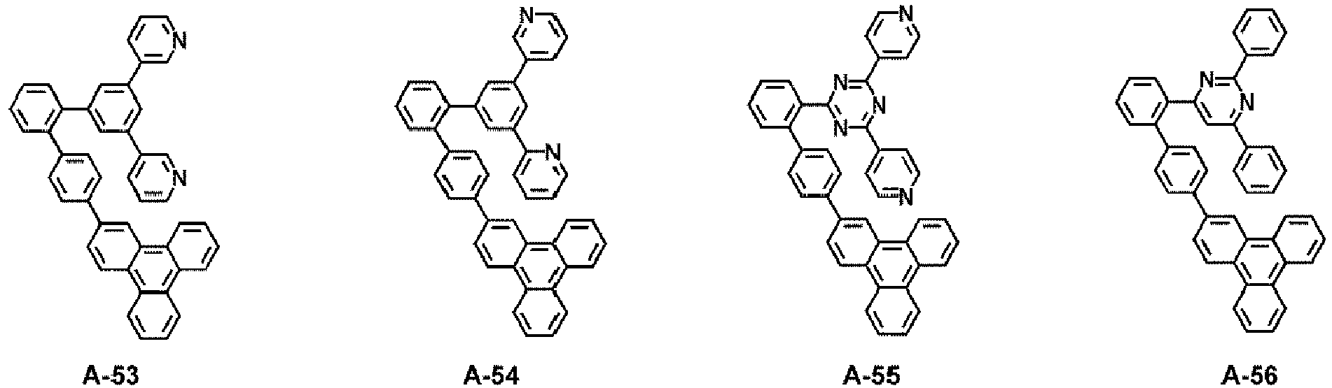





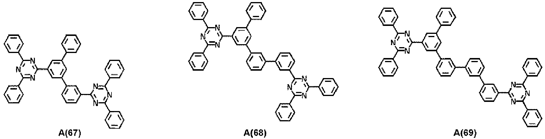


- <group HE2>




























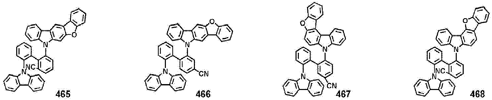






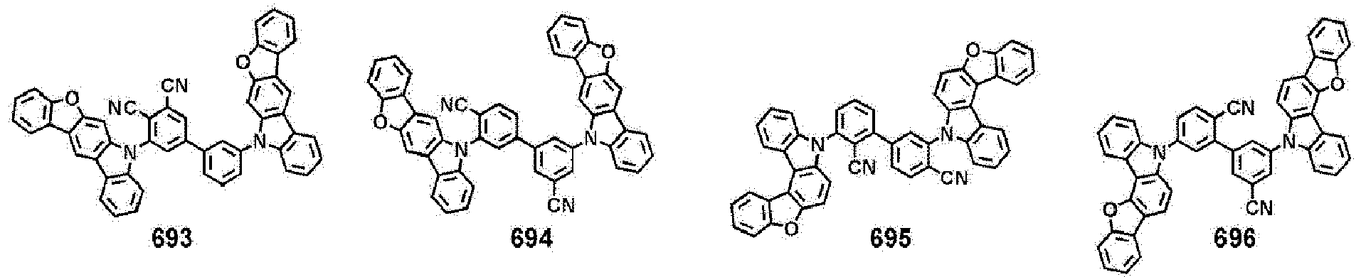











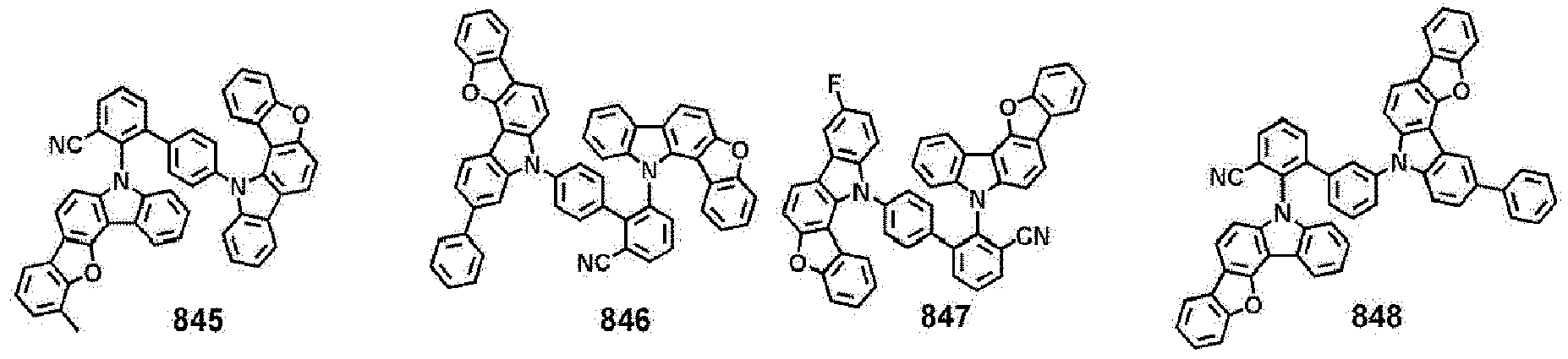

- <group HE3>


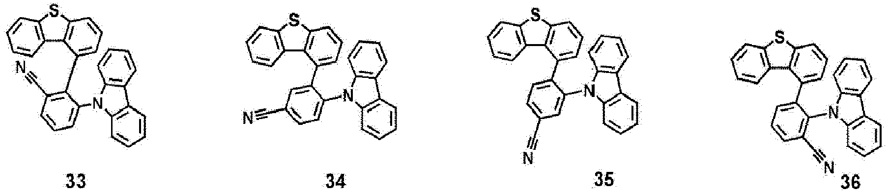


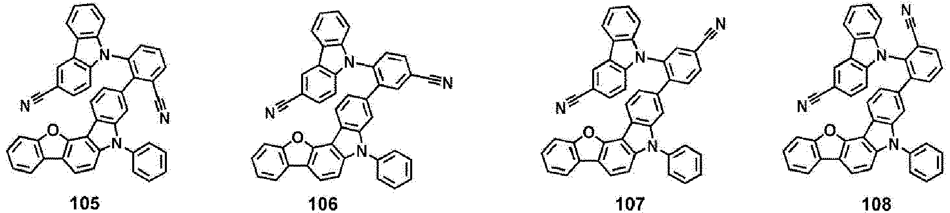




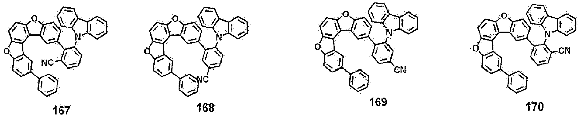








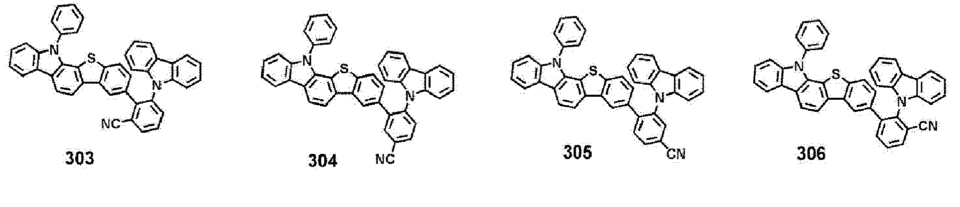





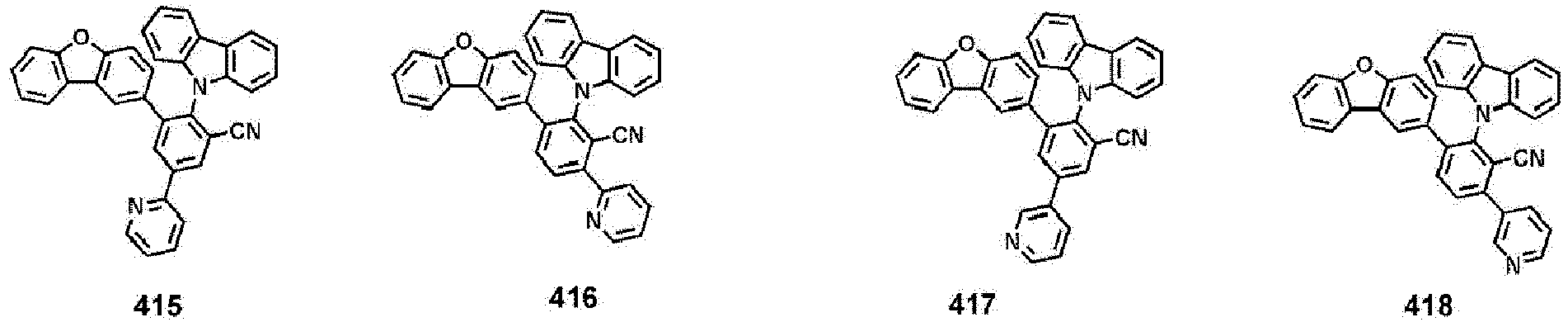


- <group HE4>


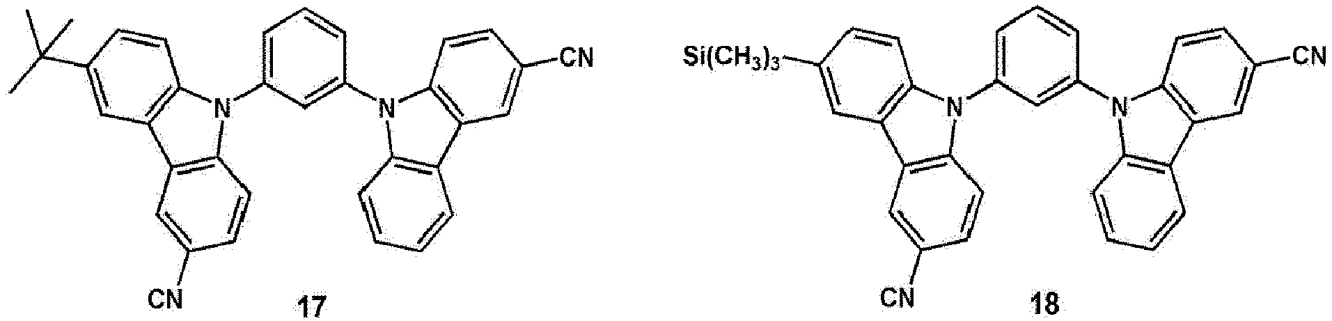

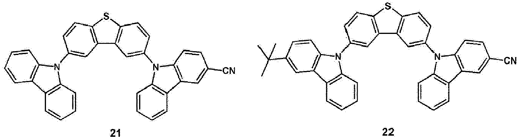


- <group HE5>




- <group HE6>
























- <group HE7>











- In one embodiment, the hole transport host may be selected from Compounds H-H1 to H-H103, but embodiments of the present disclosure are not limited thereto:


- In one embodiment, the amphiprotic host may be selected from group HEH1, but embodiments of the present disclosure are not limited thereto:
<group HEH1>




















Compounds 1 to 432,
Ph may be a phenyl group. - When the host is a mixture of an electron transport host and a hole transport host, the weight ratio of the electron transport host and hole transport host may be 1: 9 to 9: 1, for example, 2: 8 to 8: 2, for example, 4: 6 to 6: 4, for example, 5: 5. When the weight ratio of the electron transport host and the hole transport host satisfies the above-described ranges, the hole-and-electron transport balance in the
emission layer 15 may be made. - Since the cooling dopant emits fluorescent light, organic light-emitting devices according to an embodiment of the present disclosure are clearly distinguished from organic light-emitting devices containing compounds that emit phosphorescent light.
- The cooling dopant satisfies
Condition 2, as described above. - The maximum emission wavelength of the emission spectrum of the cooling dopant may be 400 nm or more and 550 nm or less. For example, the maximum emission wavelength of the emission spectrum of the cooling dopant may be 400 nm or more and 495 nm or less, or 450 nm or more and 495 nm or less, but embodiments of the present disclosure are not limited thereto. In other words, the cooling dopant may emit blue light. The "maximum emission wavelength" refers to a wavelength at which the emission intensity is the greatest, and may also be referred to as "a peak emission wavelength".
- In an embodiment, the cooling dopant may not include metal atoms.
- In an embodiment, the cooling dopant may be selected from a condensed polycyclic compound and a styryl-based compound.
- For example, the cooling dopant may include one of a naphthalene-containing core, a fluorene-containing core, a spiro-bifluorene-containing core, a benzofluorene-containing core, a dibenzofluorene-containing core, a phenanthrene-containing core, an anthracene-containing core, a fluoranthene-containing core, a triphenylene-containing core, a pyrene-containing core, a chrysene-containing core, a naphthacene-containing core, a picene-containing core, a perylene-containing core, a pentaphene-containing core, an indenoanthracene-containing core, a bisanthracene-containing core, and cores represented by Formulae 501-1 to 501-18, but embodiments of the present disclosure are not limited thereto:


- In one or more embodiments, the cooling dopant may be selected from a styryl-amine-based compound and a styryl-carbazole-based compound, but embodiments of the present disclosure are not limited thereto.
- In one embodiment, the cooling dopant may be selected from compounds represented by Formula 501:
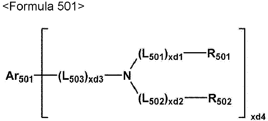
- In Formula 501,
Ar501 may be selected from: - a naphthalene group, a fluorene group, a spiro-bifluorene group, a benzofluorene group, a dibenzofluorene group, a phenanthrene group, an anthracene group, a fluoranthene group, a triphenylene group, a pyrene group, a chrysene group, a naphthacene group, a picene group, a perylene group, a pentaphene group, an indenoanthracene group, a bisanthracene group, and groups represented by Formulae 501-1 to 501-18; and
- a naphthalene group, a fluorene group, a spiro-bifluorene group, a benzofluorene group, a dibenzofluorene group, a phenanthrene group, an anthracene group, a fluoranthene group, a triphenylene group, a pyrene group, a chrysene group, a naphthacene group, a picene group, a perylene group, a pentaphene group, an indenoanthracene group, a bisanthracene group, and groups represented by Formulae 501-1 to 501-18, each substituted with at least one selected from deuterium, -F, -CI, -Br, -I, a hydroxyl group, a cyano group, a nitro group, an amino group, an amidino group, a hydrazine group, a hydrazone group, a carboxylic acid or a salt thereof, a sulfonic acid or a salt thereof, a phosphoric acid or a salt thereof, a C1-C60 alkyl group, a C2-C60 alkenyl group, a C2-C60 alkynyl group, a C1-C60 alkoxy group, a C3-C10 cycloalkyl group, a C1-C10 heterocycloalkyl group, a C3-C10 cycloalkenyl group, a C1-C10heterocycloalkenyl group, a C6-C60 aryl group, a C6-C60 aryloxy group, a C6-C60 arylthio group, a C1-C60 heteroaryl group, a monovalent non-aromatic condensed polycyclic group, a monovalent non-aromatic condensed heteropolycyclic group and -Si(Q501)(Q502)(Q503) (wherein Q501 to Q503 may each independently be selected from hydrogen, C1-C60 alkyl group, a C1-C60 alkoxy group, a C6-C60 aryl group, a C1-C60 heteroaryl group, a monovalent non-aromatic condensed polycyclic group, and a monovalent non-aromatic condensed heteropolycyclic group);
- L501 to L503 may each independently be selected from a substituted or unsubstituted C3-C10 cycloalkylene group, a substituted or unsubstituted C1-C10 heterocycloalkylene group, a substituted or unsubstituted C3-C10 cycloalkenylene group, a substituted or unsubstituted C1-C10 heterocycloalkenylene group, a substituted or unsubstituted C6-C60 arylene group, a substituted or unsubstituted C1-C60 heteroarylene group, a substituted or unsubstituted divalent non-aromatic condensed polycyclic group, and a substituted or unsubstituted divalent non-aromatic condensed heteropolycyclic group,
- R501 to R508 may each independently be selected from:
- a phenyl group, a biphenyl group, a terphenyl group, a naphthyl group, a fluorenyl group, a spiro-bifluorenyl group, a benzofluorenyl group, a dibenzofluorenyl group, a phenanthrenyl group, an anthracenyl group, a pyrenyl group, a chrysenyl group, a pyridinyl group, a pyrazinyl group, a pyrimidinyl group, a pyridazinyl group, a quinolinyl group, an isoquinolinyl group, a quinoxalinyl group, a quinazolinyl group, a carbazole group, a triazinyl group, a dibenzofuranyl group, and a dibenzothiophenyl group; and
- a phenyl group, a biphenyl group, a terphenyl group, a naphthyl group, a fluorenyl group, a spiro-bifluorenyl group, a benzofluorenyl group, a dibenzofluorenyl group, a phenanthrenyl group, an anthracenyl group, a pyrenyl group, a chrysenyl group, a pyridinyl group, a pyrazinyl group, a pyrimidinyl group, a pyridazinyl group, a quinolinyl group, an isoquinolinyl group, a quinoxalinyl group, a quinazolinyl group, a carbazolyl group, a triazinyl group, a dibenzofuranyl group, and a dibenzothiophenyl group, each substituted with at least one selected from deuterium, -F, -CI, -Br, -I, a hydroxyl group, a cyano group, a nitro group, an amino group, an amidino group, a hydrazine group, a hydrazone group, a carboxylic acid or a salt thereof, a sulfonic acid or a salt thereof, a phosphoric acid or a salt thereof, a C1-C20 alkyl group, a C1-C20 alkoxy group, a phenyl group, a biphenyl group, a terphenyl group, a naphthyl group, a fluorenyl group, a spiro-bifluorenyl group, a benzofluorenyl group, a dibenzofluorenyl group, a phenanthrenyl group, an anthracenyl group, a pyrenyl group, a chrysenyl group, a pyridinyl group, a pyrazinyl group, a pyrimidinyl group, a pyridazinyl group, a quinolinyl group, an isoquinolinyl group, a quinoxalinyl group, a quinazolinyl group, a carbazolyl group, a triazinyl group, a dibenzofuranyl group, and a dibenzothiophenyl group,
- xd1 to xd3 may each independently be selected from 0, 1, 2, and 3, and
- xd4 may be selected from 0, 1, 2, 3, 4, 5, and 6.
- For example, in Formula 501,
Ar501 may be selected from: - a naphthalene group, a fluorene group, a spiro-bifluorene group, a benzofluorene group, a dibenzofluorene group, a phenanthrene group, an anthracene group, a fluoranthene group, a triphenylene group, a pyrene group, a chrysene group, a naphthacene group, a picene group, a perylene group, a pentaphene group, an indenoanthracene group, a bisanthracene group, and groups represented by Formulae 501-1 to 501-18; and
- a naphthalene group, a fluorene group, a spiro-bifluorene group, a benzofluorene group, a dibenzofluorene group, a phenanthrene group, an anthracene group, a fluoranthene group, a triphenylene group, a pyrene group, a chrysene group, a naphthacene group, a picene group, a perylene group, a pentaphene group, an indenoanthracene group, a bisanthracene group, and groups represented by Formula 501-1 to 501-18, each substituted with at least one selected from deuterium, -F, -CI, -Br, -I, a hydroxyl group, a cyano group, a nitro group, an amino group, an amidino group, a hydrazine group, a hydrazone group, a carboxylic acid or a salt thereof, a sulfonic acid or a salt thereof, a phosphoric acid or a salt thereof, a C1-C20 alkyl group, a C1-C20 alkoxy group, a phenyl group, a biphenyl group, a terphenyl group, a naphthyl group, a fluorenyl group, a dibenzofuranyl group, a dibenzothiophenyl group, a carbazolyl group, a pyridinyl group, a pyrimidinyl group, a triazinyl group, a quinolinyl group, an isoquinolinyl group and -Si(Q501)(Q502)(Q503) (Q501 to Q503 may each independently be selected from hydrogen, C1-C20 alkyl group, a C1-C20 alkoxy group, a phenyl group, a biphenyl group, a terphenyl group, and a naphthyl group),
- xd1 to xd3 may each independently be selected from 0, 1, and 2, and
- xd4 may be selected from 0, 1, 2, and 3, but embodiments of the present disclosure are not limited thereto.
- In one or more embodiments, the cooling dopant may include a compound represented by one of Formulae 502-1 to 502-5:


- X51 may be N or C-[(L501)xd1-R501], X52 may be N or C-[(L502)xd2-R502], X53 may be N or C-[(L503)xd3-R503], X54 may be N or C-[(L504)xd4-R504], X55 may be N or C-[(L505)xd5-R505], X56 may be N or C-[(L506)xd6-R506], X57 may be N or C-[(L507)xd7-R507], and X58 may be N or C-[(L508)xd8-R508],
- L501 to L508 are each the same as described in connection with L501 in Formula 501,
- xd1 to xd8 are each the same as described in connection with xd1 in Formula 501,
- R501 to R508 may each independently be selected from:
- hydrogen, deuterium, -F, -CI, -Br, -I, a hydroxyl group, a cyano group, a nitro group, an amino group, an amidino group, a hydrazine group, a hydrazone group, a carboxylic acid or a salt thereof, a sulfonic acid or a salt thereof, a phosphoric acid or a salt thereof, a C1-C20 alkyl group, a C1-C20 alkoxy group,
- a phenyl group, a biphenyl group, a terphenyl group, a naphthyl group, a fluorenyl group, a spiro-bifluorenyl group, a benzofluorenyl group, a dibenzofluorenyl group, a phenanthrenyl group, an anthracenyl group, a pyrenyl group, a chrysenyl group, a pyridinyl group, a pyrazinyl group, a pyrimidinyl group, a pyridazinyl group, a quinolinyl group, an isoquinolinyl group, a quinoxalinyl group, a quinazolinyl group, a carbazole group, a triazinyl group, a dibenzofuranyl group, and a dibenzothiophenyl group; and
- a phenyl group, a biphenyl group, a terphenyl group, a naphthyl group, a fluorenyl group, a spiro-bifluorenyl group, a benzofluorenyl group, a dibenzofluorenyl group, a phenanthrenyl group, an anthracenyl group, a pyrenyl group, a chrysenyl group, a pyridinyl group, a pyrazinyl group, a pyrimidinyl group, a pyridazinyl group, a quinolinyl group, an isoquinolinyl group, a quinoxalinyl group, a quinazolinyl group, a carbazolyl group, a triazinyl group, a dibenzofuranyl group, and a dibenzothiophenyl group, each substituted with at least one selected from deuterium, -F, -CI, -Br, -I, a hydroxyl group, a cyano group, a nitro group, an amino group, an amidino group, a hydrazine group, a hydrazone group, a carboxylic acid or a salt thereof, a sulfonic acid or a salt thereof, a phosphoric acid or a salt thereof, a C1-C20 alkyl group, a C1-C20 alkoxy group, a phenyl group, a biphenyl group, a terphenyl group, a naphthyl group, a fluorenyl group, a spiro-bifluorenyl group, a benzofluorenyl group, a dibenzofluorenyl group, a phenanthrenyl group, an anthracenyl group, a pyrenyl group, a chrysenyl group, a pyridinyl group, a pyrazinyl group, a pyrimidinyl group, a pyridazinyl group, a quinolinyl group, an isoquinolinyl group, a quinoxalinyl group, a quinazolinyl group, a carbazolyl group, a triazinyl group, a dibenzofuranyl group, and a dibenzothiophenyl group,
- xd11 and xd12 may each independently be an integer from 0 to 5, and
- two of R501 to R504 may optionally be linked together to form a saturated or unsaturated ring, and
- two of R505 to R508 may optionally be linked together to form a saturated or unsaturated ring.
- The cooling dopant may include at least one compound selected from, for example, the following compounds FD(1) to FD(16) and FD1 to FD18:


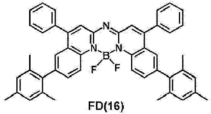


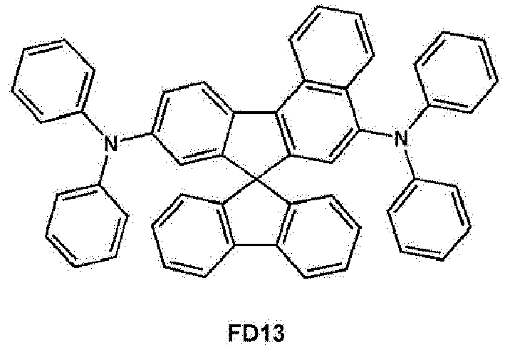


- The amount of the cooling dopant in the emission layer may be from about 0.01 wt% to about 15 wt%, but embodiments of the present disclosure are not limited thereto.
- The sensitizer may include Pt. In one embodiment, the sensitizer may be an organic metallic compound containing Pt.
- In one embodiment, the sensitizer may include Pt and an organic ligand (L11), and L11 and Pt may form 1, 2, 3, or 4 cyclometalated rings.
- In an embodiment, the sensitizer may include an organometallic compound represented by Formula 101:
<Formula 101> Pt(L11)n11(L12)n12
wherein, inFormula 101, - L11 is a ligand represented by one of Formulae 1-1 to 1-4;
- L12 may be selected from a monodentate ligand and a bidentate ligand;
- n11 may be 1,
- n12 may be selected from 0, 1, and 2;

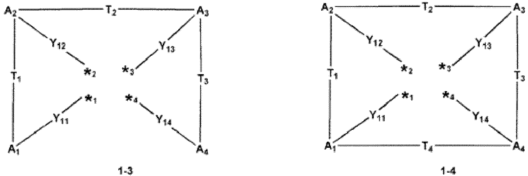
- A1 to A4 may each independently be selected from a substituted or unsubstituted C5-C30 carbocyclic group, a substituted or unsubstituted C1-C30 heterocyclic group, and a non-cyclic group,
- Y11 to Y14 may each independently be a chemical bond, O, S, N(R91), B(R91), P(R91), or C(R91)(R92),
- T1 to T4 may each independently be selected from a single bond, a double bond, ∗-N(R93)-∗', ∗-B(R93)-∗', ∗-P(R93)-∗', ∗-C(R93)(R94)-∗', ∗-Si(R93)(R94)-∗', ∗-Ge(R93)(R94)-∗', ∗-S-∗', ∗-Se-∗', ∗-0-∗', ∗-C(=O)-∗', ∗-S(=O)-∗', ∗-S(=O)2-∗', ∗-C(R93)=∗', ∗=C(R93)-∗', ∗-C(R93)=C(R94)-∗', ∗-C(=S)-∗', and ∗-C≡C-∗',
- a substituent of the substituted C5-C30 carbocyclic group, a substituent of substituted C1-C30 heterocyclic group, and R91 to R94 may each independently be selected from hydrogen, deuterium, -F, -CI, -Br, -I, -SF5, a hydroxyl group, a cyano group, a nitro group, an amidino group, a hydrazine group, a hydrazone group, a carboxylic acid or a salt thereof, a sulfonic acid or a salt thereof, a phosphoric acid or a salt thereof, a substituted or unsubstituted C1-C60 alkyl group, a substituted or unsubstituted C2-C60 alkenyl group, a substituted or unsubstituted C2-C60 alkynyl group, a substituted or unsubstituted C1-C60 alkoxy group, a substituted or unsubstituted C3-C10 cycloalkyl group, a substituted or unsubstituted C1-C10 heterocycloalkyl group, a substituted or unsubstituted C3-C10 cycloalkenyl group, a substituted or unsubstituted C1-C10heterocycloalkenyl group, a substituted or unsubstituted C6-C60 aryl group, a substituted or unsubstituted C6-C60 aryloxy group, a substituted or unsubstituted C6-C60 arylthio group, a substituted or unsubstituted C1-C60 heteroaryl group, a substituted or unsubstituted monovalent non-aromatic condensed polycyclic group, a substituted or unsubstituted monovalent non-aromatic condensed heteropolycyclic group, -Si(Q1)(Q2)(Q3), -B(Q1)(Q2), -N(Q1)(Q2), -P(Q1)(Q2), -C(=O)(Q1), -S(=O)(Q1), -S(=O)2(Q1), -P(=O)(Q1)(Q2), and -P(=S)(Q1)(Q2), wherein each of a substituent of the substituted C5-C30 carbocyclic group and a substituent of substituted C1-C30 heterocyclic group is not hydrogen,
- ∗ 1, ∗ 2, ∗ 3, and ∗ 4 each indicate a binding site to Pt, and
- Q1 to Q3 may each independently selected from hydrogen, deuterium, -F, -CI, -Br, -I, a hydroxyl group, a cyano group, a nitro group, an amidino group, a hydrazine group, a hydrazone group, a C1-C60 alkyl group, a C2-C60 alkenyl group, a C2-C60 alkynyl group, a C1-C60 alkoxy group, a C3-C10 cycloalkyl group, a C1-C10 heterocycloalkyl group, a C3-C10 cycloalkenyl group, a C1-C10 heterocycloalkenyl group, a C6-C60 aryl group, a C7-C60 alkyl aryl group, a C6-C60 aryloxy group, a C6-C60 arylthio group, a C1-C60 heteroaryl group, a C2-C60 alkyl heteroaryl group, a C1-C60 heteroaryloxy group, a C1-C60 heteroarylthio group, a monovalent non-aromatic condensed polycyclic group, a monovalent non-aromatic condensed heteropolycyclic group, a C1-C60 alkyl group that is substituted with at least one selected from deuterium, -F, a cyano group, a C1-C60 alkyl group, and a C6-C60 aryl group, and a C6-C60 aryl group that is substituted with at least one selected from deuterium, -F, a cyano group, a C1-C60 alkyl group, and a C6-C60 aryl group.
- In one or more embodiments, the sensitizer may be selected from Groups I, II, III, V and VI, but embodiments of the present disclosure are not limited thereto:
<Group I>





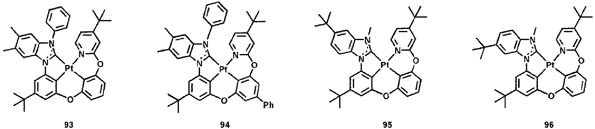




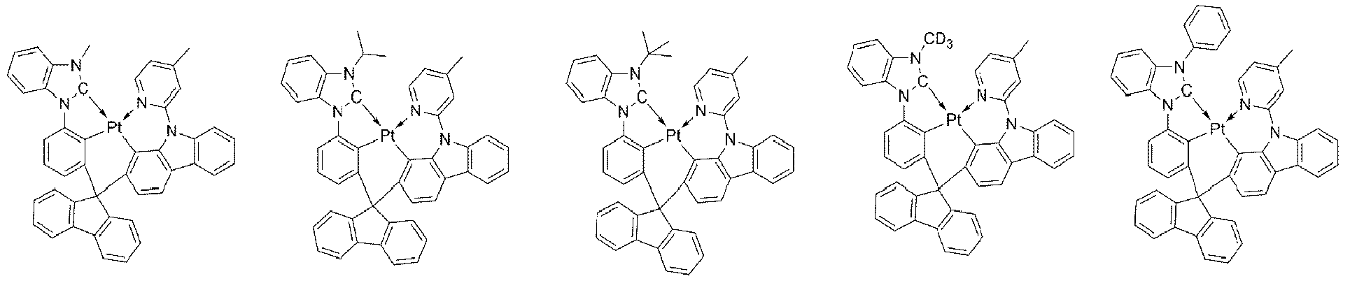


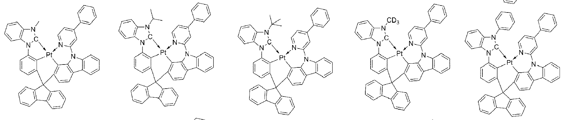


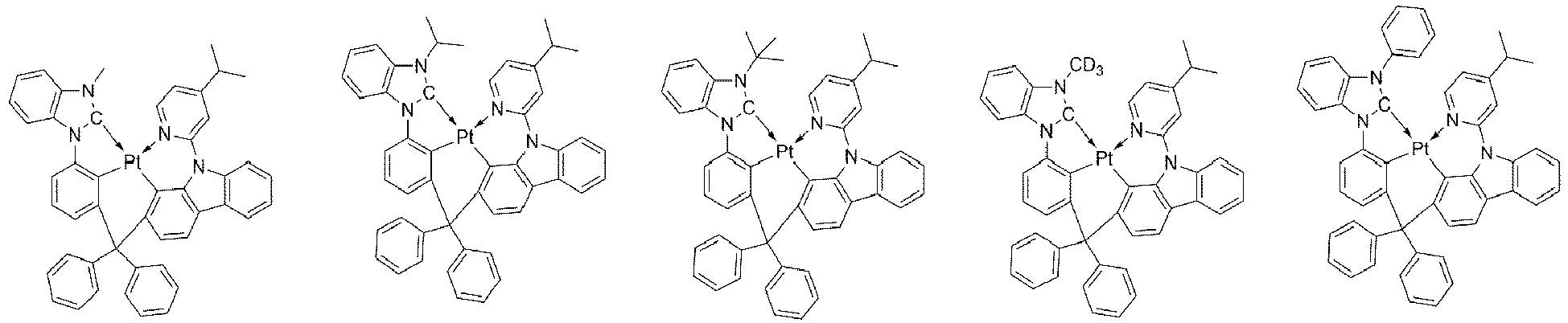


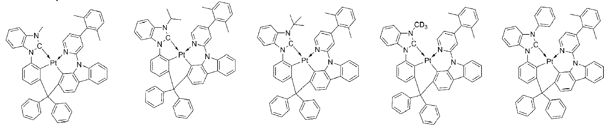











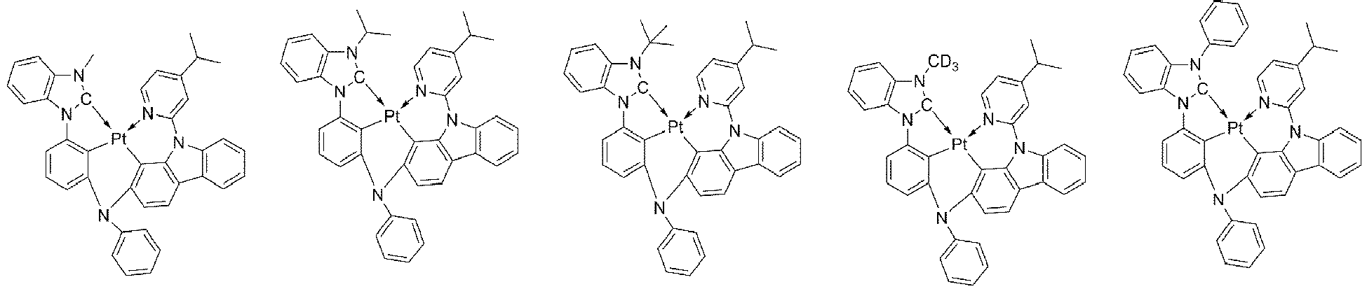


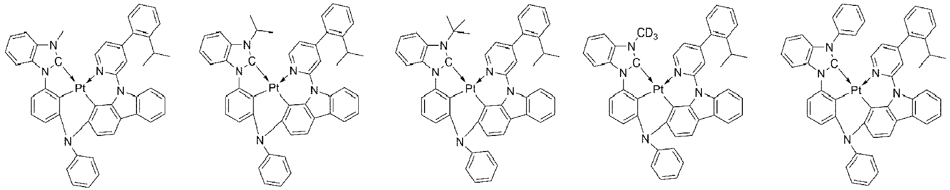





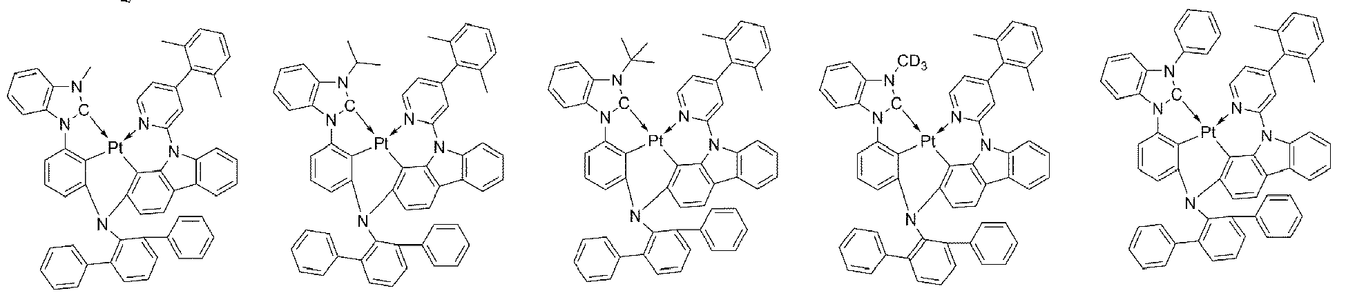


a compound represented by Formula A below:
<Formula A> (L101)n101-M101-(L102)m101
L101, n101, M101, L102, and m101 in Formula A are the same as shown in Table 1:Table 1 Compound name L101 n101 M101 L102 m101 BD263 LM11 2 Pt - 0 BD264 LM13 2 Pt - 0 BD265 LM15 2 Pt - 0 BD266 LM45 2 Pt - 0 BD267 LM47 2 Pt - 0 BD268 LM49 2 Pt - 0 BD269 LM98 2 Pt - 0 BD270 LM100 2 Pt - 0 BD271 LM102 2 Pt - 0 BD272 LM132 2 Pt - 0 BD273 LM134 2 Pt - 0 BD274 LM136 2 Pt - 0 BD275 LM151 2 Pt - 0 BD276 LM153 2 Pt - 0 BD277 LM158 2 Pt - 0 BD278 LM180 2 Pt - 0 BD279 LM182 2 Pt - 0 BD280 LM187 2 Pt - 0 BD281 LM201 2 Pt - 0 BD282 LM206 2 Pt - 0 BD283 LM211 2 Pt - 0 BD284 LM233 2 Pt - 0 BD285 LM235 2 Pt - 0 BD286 LM240 2 Pt - 0 BD287 LFM5 2 Pt - 0 BD288 LFM6 2 Pt - 0 BD289 LFM7 2 Pt - 0 BD290 LFP5 2 Pt - 0 BD291 LFP6 2 Pt - 0 BD292 LFP7 2 Pt - 0 BD293 LM47 1 Pt AN1 1 BD294 LM47 1 Pt AN2 1 BD295 LM47 1 Pt AN3 1 BD296 LM47 1 Pt AN4 1 BD297 LM47 1 Pt AN5 1 

Table 2 Formula 1-1 Ligand name R11 R12 R13 R14 R15 R16 R17 R18 R19 R20 LM11 Y3 D Y11 D Y3 D D D D D LM13 Y3 D Y11 D Y3 D Y3 D D D LM15 Y3 D Y11 D Y3 D Y12 D D D LM45 Y3 D Y12 D Y3 D D D D D LM47 Y3 D Y12 D Y3 D Y3 D D D LM49 Y3 D Y12 D Y3 D Y12 D D D LM98 Y10 D Y13 D Y10 D D D D D LM100 Y10 D Y13 D Y10 D Y3 D D D LM102 Y10 D Y13 D Y10 D Y12 D D D LM132 Y10 D Y14 D Y10 D D D D D LM134 Y10 D Y14 D Y10 D Y3 D D D LM136 Y10 D Y14 D Y10 D Y12 D D D LM151 Y3 D Y15 D Y3 D D D D D LM153 Y3 D Y15 D Y3 D Y3 D D D LM158 Y3 D Y15 D Y3 D Y12 D D D LM180 Y10 D Y15 D Y10 D D D D D LM182 Y10 D Y15 D Y10 D Y3 D D D LM187 Y10 D Y15 D Y10 D Y12 D D D LM201 Y3 Y15 D D Y3 D D D D D LM206 Y3 Y15 D D Y3 D Y3 D D D LM211 Y3 Y15 D D Y3 D Y12 D D D LM233 Y10 Y15 D D Y10 D D D D D LM235 Y10 Y15 D D Y10 D Y3 D D D LM240 Y10 Y15 D D Y10 D Y12 D D D [Table 3] Formula 1-2 Ligand name R11 X11 R101 R102 R103 R104 R14 R15 R16 R17 R18 R19 R20 LFM5 Y10 O D D D D D Y10 D D D D D LFM6 Y10 O D D D D D Y10 D Y3 D D D LFM7 Y10 O D D D D D Y10 D Y12 D D D Table 4 Formula 1-3 Ligand name R11 X11 R101 R102 R103 R104 R14 R15 R16 R17 R18 R19 R20 LFP5 Y10 O D D D D D Y10 D D D D D LFP6 Y10 O D D D D D Y10 D Y3 D D D LFP7 Y10 O D D D D D Y10 D Y12 D D D 

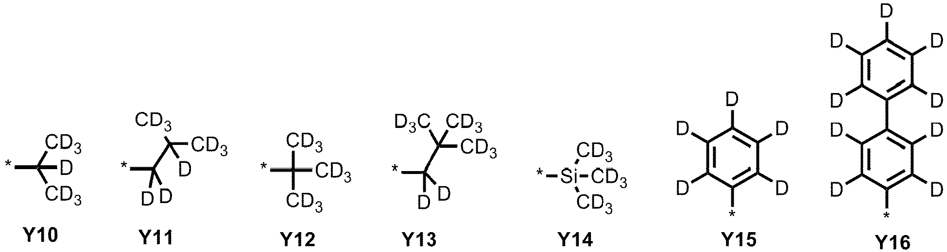


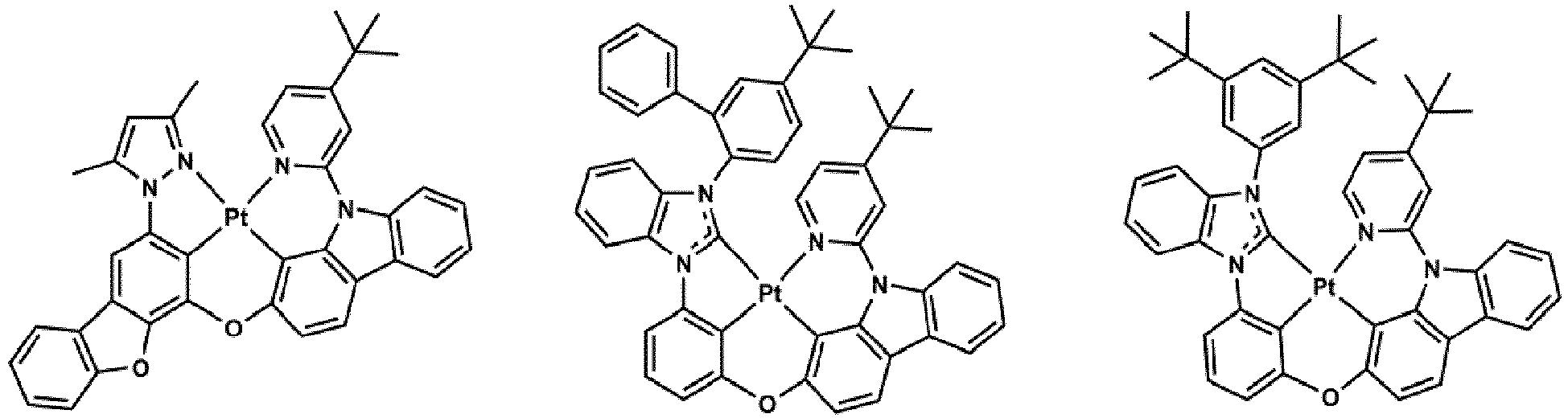
- In one or more embodiments, the sensitizer may be a thermally activated delayed fluorescence emitter. Thermally activated delayed fluorescence emitter may not include metal. In one embodiment, thermally activated delayed fluorescence emitter may satisfy Condition 7:

Δ EST is the difference between the lowest excitation singlet energy level and the lowest excitation triplet energy level of the sensitizer. - In one embodiment, the sensitizer may include thermally activated delayed fluorescence emitter represented by Formula 201 or 202:

- A21 is an acceptor group,
- D21 is a donor group,
- m21 may be 1, 2, or 3, and n21 may be 1, 2, or 3,
- the sum of n21 and m21 in Formula 201 may be 6 or less, and the sum of n21 and m21 in Formula 202 may be 5 or less,
- R21 may be selected from hydrogen, deuterium, -F, -Cl, -Br, -I, SF5, a hydroxyl group, a cyano group, a nitro group, an amidino group, a hydrazine group, a hydrazone group, a substituted or unsubstituted C1-C60 alkyl group, a substituted or unsubstituted C2-C60 alkenyl group, a substituted or unsubstituted C2-C60 alkynyl group, a substituted or unsubstituted C1-C60 alkoxy group, a substituted or unsubstituted C3-C10 cycloalkyl group, a substituted or unsubstituted C1-C10 heterocycloalkyl group, a substituted or unsubstituted C3-C10 cycloalkenyl group, a substituted or unsubstituted C1-C10 heterocycloalkenyl group, a substituted or unsubstituted C6-C60 aryl group, a substituted or unsubstituted C7-C60 alkylaryl group, a substituted or unsubstituted C6-C60 aryloxy group, a substituted or unsubstituted C6-C60 arylthio group, a substituted or unsubstituted C1-C60 heteroaryl group, a substituted or unsubstituted C2-C60 alkylheteroaryl group, a substituted or unsubstituted C1-C60heteroaryloxy group, a substituted or unsubstituted C1-C60 heteroarylthio group, a substituted or unsubstituted monovalent non-aromatic condensed polycyclic group, a substituted or unsubstituted monovalent non-aromatic condensed heteropolycyclic group, -Si(Q1)(Q2)(Q3), -B(Q1)(Q2), -N(Q1)(Q2), -P(Q1)(Q2), -C(=O)(Q1), -S(=O)(Q1), -S(=O)2(Q1), -P(=O)(Q1)(Q2), and -P(=S)(Q1)(Q2), a plurality of R21 may optionally be linked together to form a substituted or unsubstituted C5-C30 carbocyclic group or a substituted or unsubstituted C1-C30 heterocyclic group,
- Q1 to Q3 may each independently selected from hydrogen, deuterium, -F, -Cl, -Br, -I, a hydroxyl group, a cyano group, a nitro group, an amidino group, a hydrazine group, a hydrazone group, a C1-C60 alkyl group, a C2-C60 alkenyl group, a C2-C60 alkynyl group, a C1-C60 alkoxy group, a C3-C10 cycloalkyl group, a C1-C10 heterocycloalkyl group, a C3-C10 cycloalkenyl group, a C1-C10heterocycloalkenyl group, a C6-C60 aryl group, a C7-C60 alkyl aryl group, a C6-C60 aryloxy group, a C6-C60 arylthio group, a C1-C60 heteroaryl group, a C2-C60 alkyl heteroaryl group, a C1-C60 heteroaryloxy group, a C1-C60 heteroarylthio group, a monovalent non-aromatic condensed polycyclic group, a monovalent non-aromatic condensed heteropolycyclic group, a C1-C60 alkyl group that is substituted with at least one selected from deuterium, -F, a cyano group, a C1-C60 alkyl group, and a C6-C60 aryl group, and a C6-C60 aryl group that is substituted with at least one selected from deuterium, -F, a cyano group, a C1-C60 alkyl group, and a C6-C60 aryl group.
- For example, A21 in Formula 201 and 202 may be a substituted or unsubstituted π electron-deficient nitrogen-free cyclic group.
- In one embodiment, the π electron-deficient nitrogen-free cyclic group may be selected from a benzene group, a heptalene group, an indene group, a naphthalene group, an azulene group, an indacene group, acenaphthylene group, a fluorene group, a spiro-bifluorene group, a benzofluorene group, a dibenzofluorene group, a phenalene group, a phenanthrene group, an anthracene group, a fluoranthene group, a triphenylene group, a pyrene group, a chrysene group, a naphthacene group, a picene group, a perylene group, a pentacene group, a hexacene group, a pentaphene group, a rubicene group, a coronene group, an ovalene group, a pyrrole group, an isoindole group, an indole group, a furan group, a thiophene group, a benzofuran group, a benzothiophene group, a benzocarbazole group, a dibenzocarbazole group, a dibenzofuran group, a dibenzothiophene group, a dibenzothiophene sulfone group, a carbazole group, a dibenzosilole group, an indenocarbazole group, an indolocarbazole group, a benzofurocarbazole group, a benzothienocarbazole group, a triindolobenzene group; and a condensed cyclic group of two or more π electron-deficient nitrogen-free cyclic groups, but embodiments of the present disclosure are not limited thereto.
- For example, D21 in Formulae 201 and 202 may be selected from: -F, a cyano group, and an π-electron deficient nitrogen-containing cyclic group;
a C1-C60 alkyl group, a π-electron deficient nitrogen-containing cyclic group, and a π electron-deficient nitrogen-free cyclic group, each substituted with at least one selected from -F and a cyano group; and
a π-electron deficient nitrogen-containing cyclic group, each substituted with at least one selected from deuterium, a C1-C60 alkyl group, an π-electron deficient nitrogen-containing cyclic group, and an π electron-deficient nitrogen-free cyclic group. - In one embodiment, the π electron-deficient nitrogen-free cyclic group is the same as described above.
- The term "π electron-deficient nitrogen-containing cyclic group" used herein refers to a cyclic group having at least one *-N=*' moiety, and, for example, may be selected from an imidazole group, a pyrazole group, a thiazole group, an isothiazole group, an oxazole group, an isoxazole group, a pyridine group, a pyrazine group, a pyridazine group, a pyrimidine group, an indazole group, a purine group, a quinoline group, an isoquinoline group, a benzoquinoline group, a phthalazine group, a naphthyridine group, a quinoxaline group, a quinazoline group, a cinnoline group, a phenanthridine group, an acridine group, a phenanthroline group, a phenazine group, a benzimidazole group, an isobenzothiazole group, a benzoxazole group, an isobenzoxazole group, a triazole group, a tetrazole group, an oxadiazole group, a triazine group, a thiadiazole group, an imidazopyridine group, an imidazopyrimidine group, an azacarbazole group, and a benzimidazolobenzimidazole group; and a condensed cyclic group in which two or more π electron-deficient nitrogen-containing cyclic groups are condensed with each other.
- In one or more embodiments, the sensitizer may be selected from Groups VII to XI, but embodiments of the present disclosure are not limited thereto:
- <group VII>


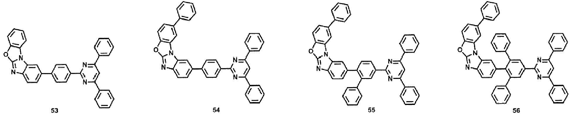


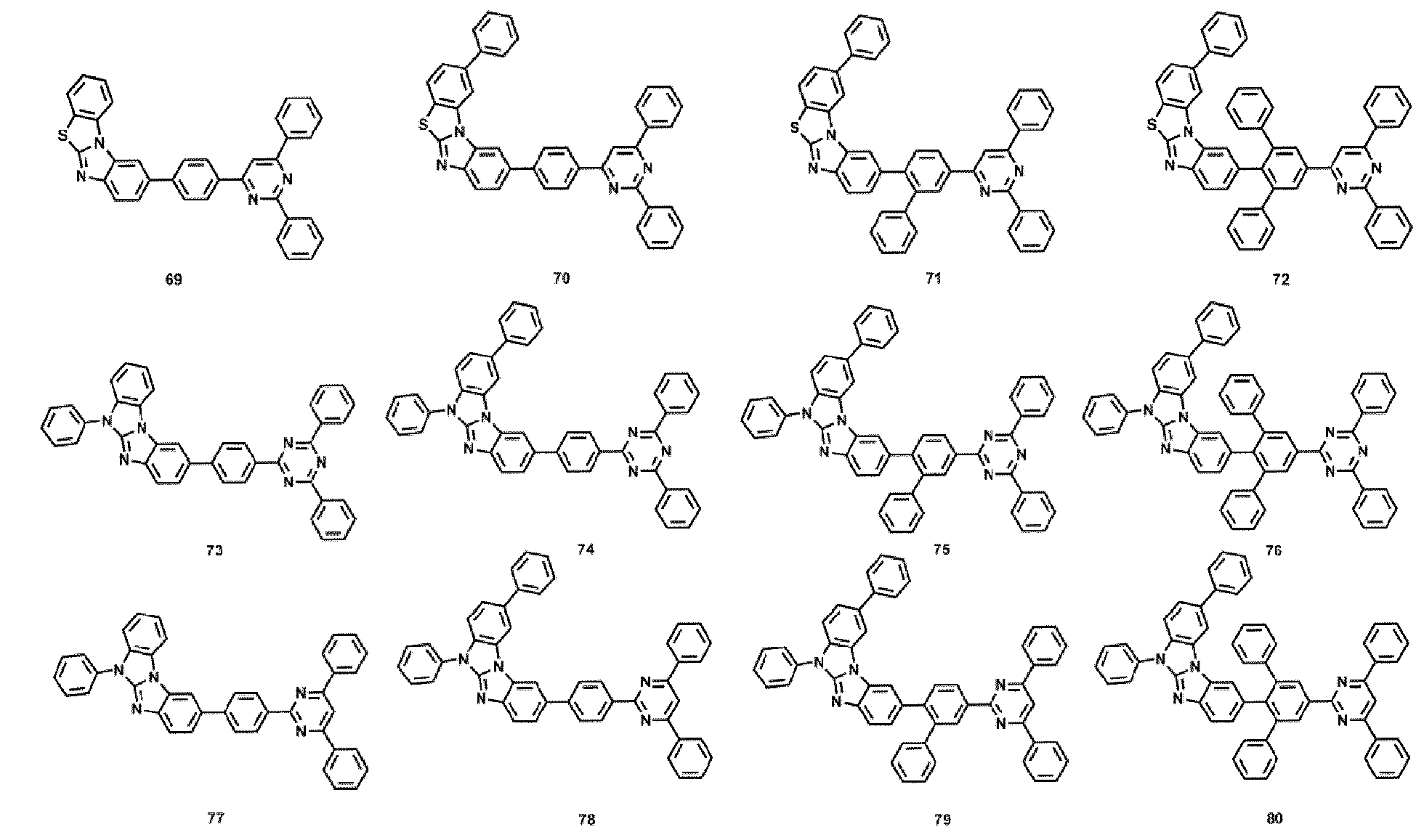


- <group VIII>


- <Group IX>



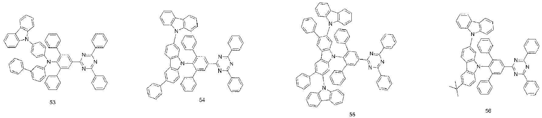


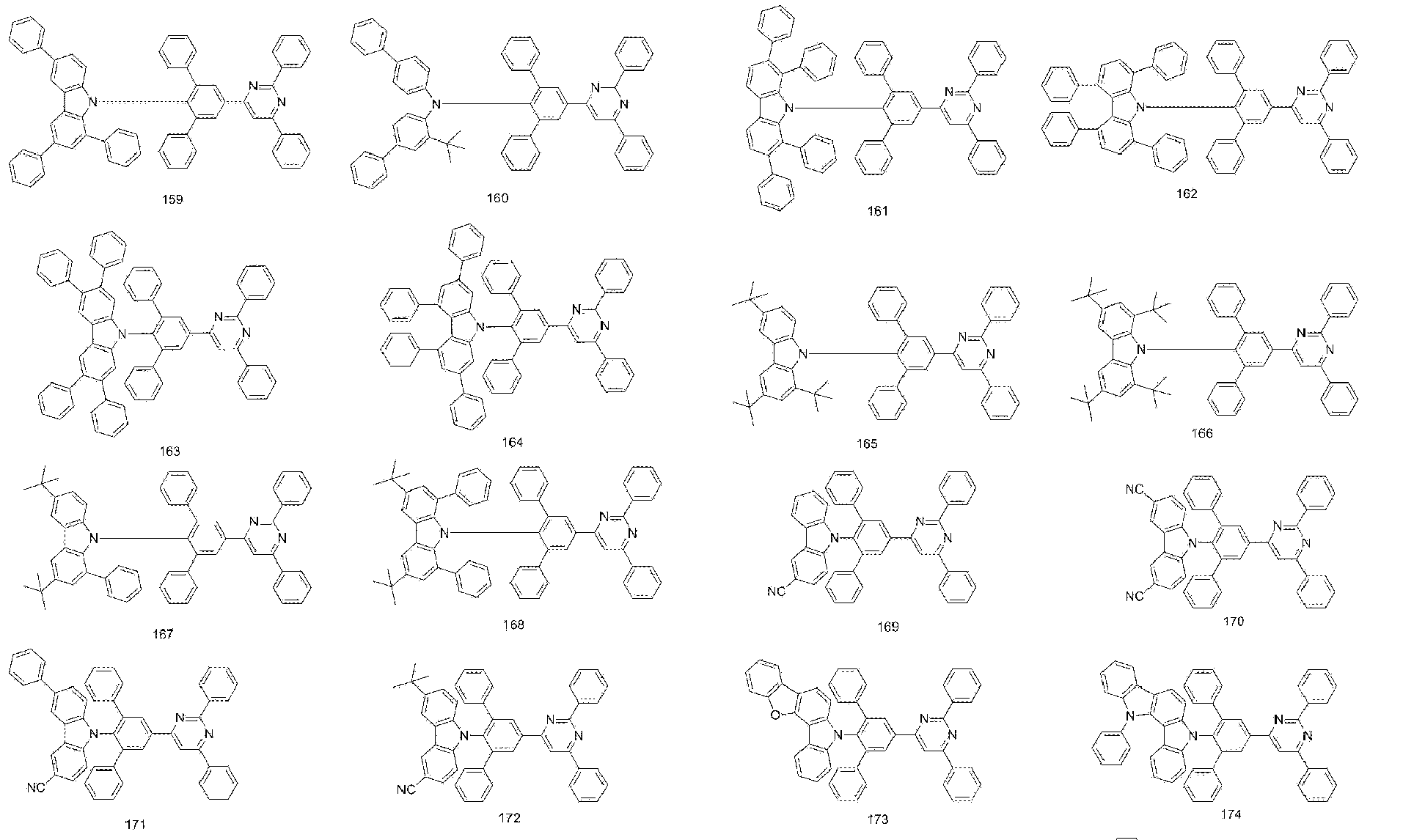








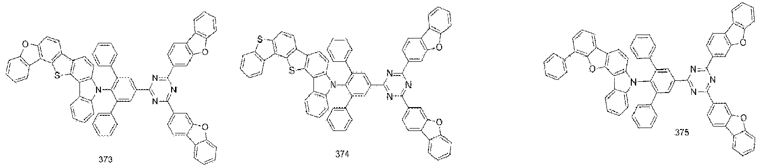


- <group X>


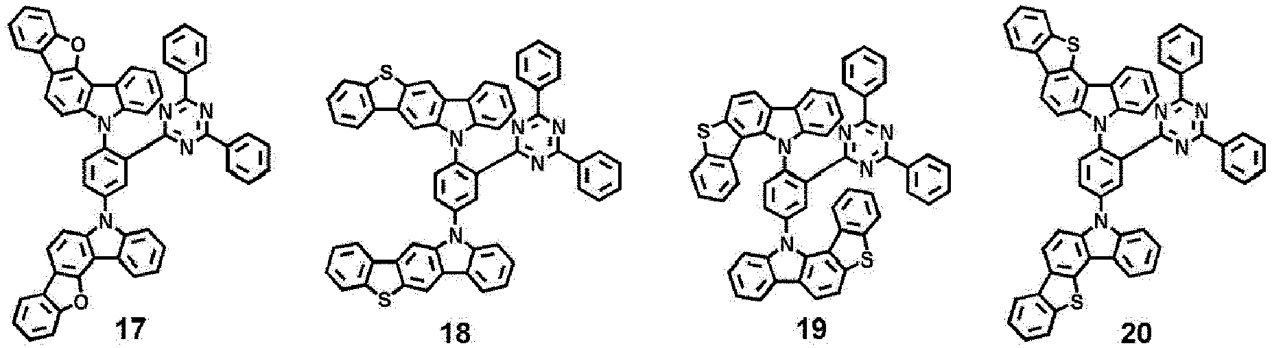


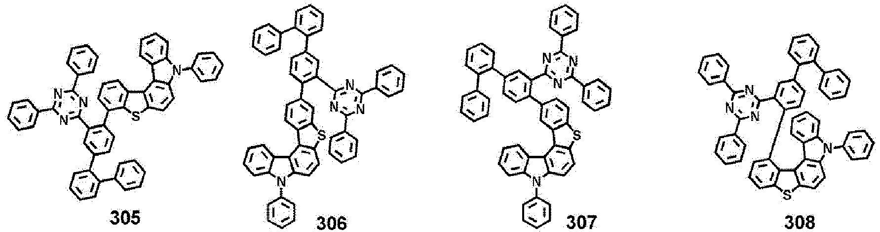


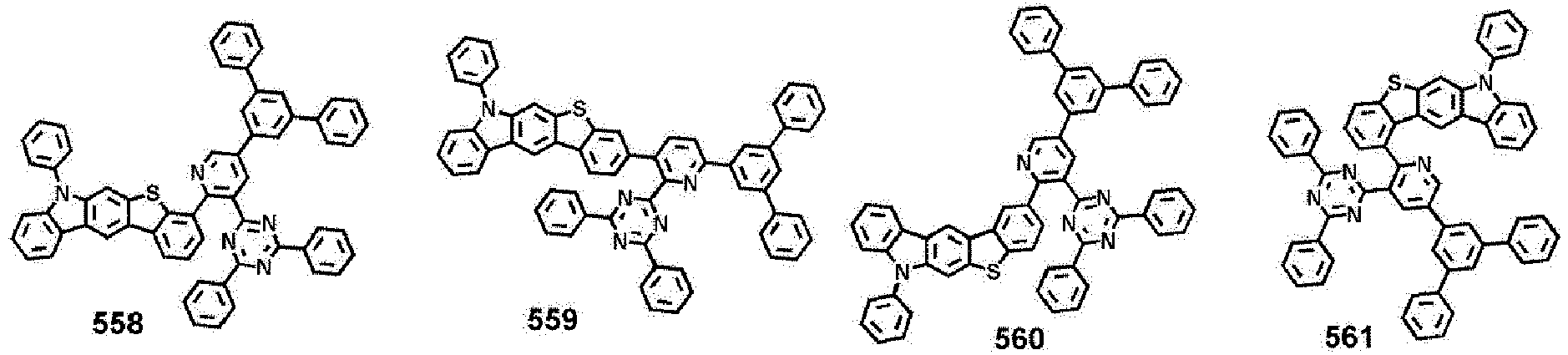


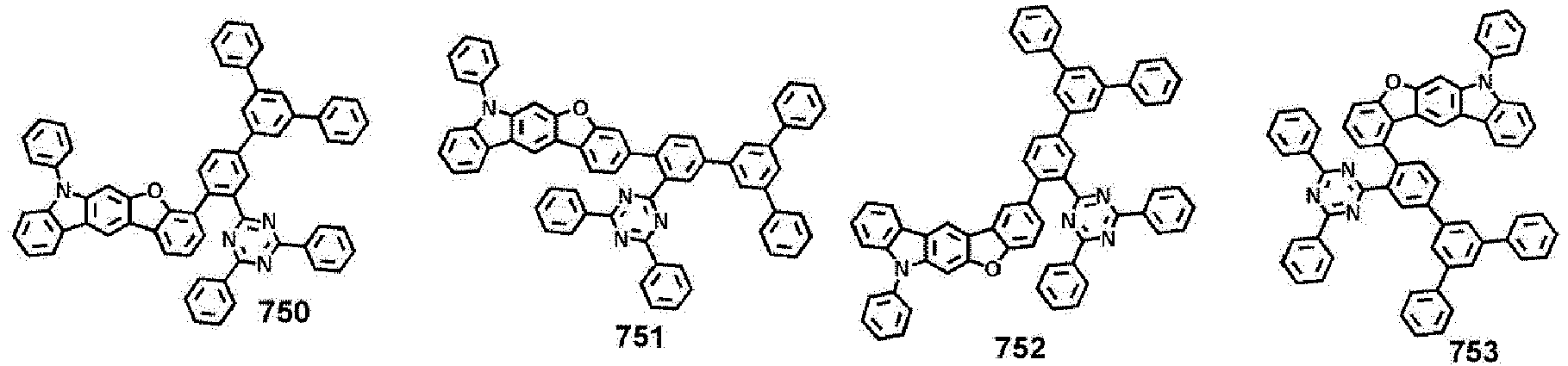


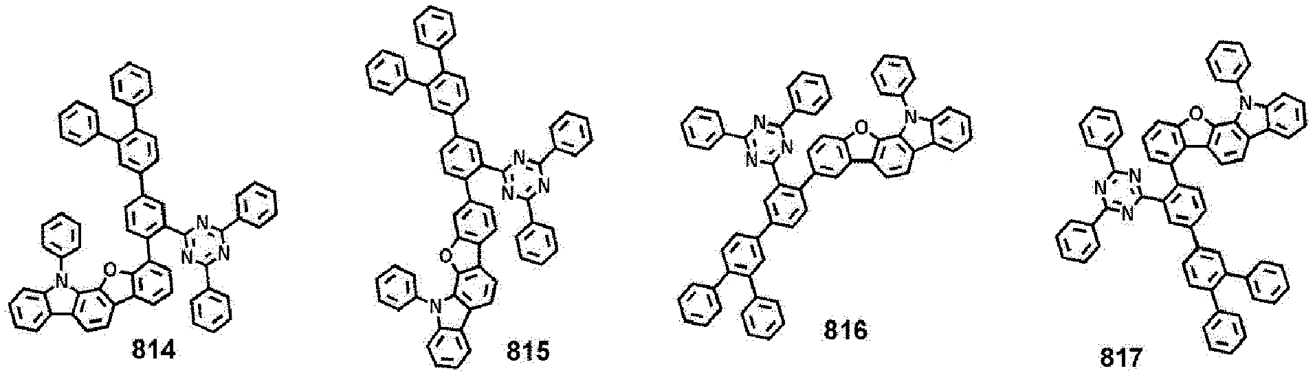


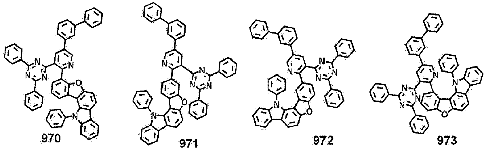


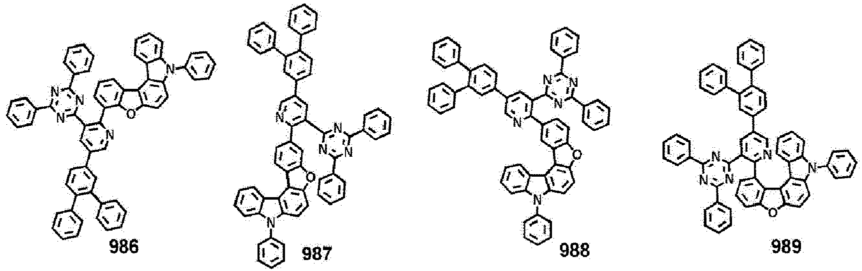


- <group XI>

- The
hole transport region 12 may be located between thefirst electrode 11 and theemission layer 15 of the organic light-emitting device 10. - The
hole transport region 12 may have a single-layered structure or a multi-layered structure. - For example, the
hole transport region 12 may have a hole injection layer, a hole transport layer, a hole injection layer/hole transport layer structure, a hole injection layer/first hole transport layer/second hole transport layer structure, a hole transport layer/middle layer structure, a hole injection layer/hole transport layer/middle layer structure, a hole transport layer/electron blocking layer or hole injection layer/hole transport layer/electron blocking layer structure, but embodiments of the present disclosure are not limited thereto. - The
hole transport region 12 may include any compound having hole transport properties. - For example, the
hole transport region 12 may include an amine-based compound. - In one embodiment, the
hole transport region 1 may include at least one selected from a compound represented by Formula 201 to a compound represented by Formula 205, but embodiments of the present disclosure are not limited thereto:


- L201 to L209 may each independently *-be O-*', *-S-*', a substituted or unsubstituted C5-C60 carbocyclic group, or a substituted or unsubstituted C1-C60 heterocyclic group,
- xa1 to xa9 may each independently be an integer from 0 to 5, and
- R201 to R206 may each independently be selected from a substituted or unsubstituted C3-C10 cycloalkyl group, a substituted or unsubstituted C1-C10 heterocycloalkyl group, a substituted or unsubstituted C3-C10 cycloalkenyl group, a substituted or unsubstituted C1-C10heterocycloalkenyl group, a substituted or unsubstituted C6-C60 aryl group, a substituted or unsubstituted C6-C60 aryloxy group, a substituted or unsubstituted C6-C60 arylthio group, a substituted or unsubstituted C1-C60 heteroaryl group, a substituted or unsubstituted monovalent non-aromatic condensed polycyclic group, and a substituted or unsubstituted monovalent non-aromatic condensed heteropolycyclic group, wherein neighboring two groups of R201 to R206 may optionally be linked to each other via a single bond, a dimethyl-methylene group, or a diphenyl-methylene group.
- For example,
L201 to L209 may be selected from a benzene group, a heptalene group, an indene group, a naphthalene group, an azulene group, a heptalene group, an indacene group, an acenaphthylene group, a fluorene group, a spiro-bifluorene group, a benzofluorene group, a dibenzofluorene group, a phenalene group, a phenanthrene group, an anthracene group, a fluoranthene group, a triphenylene group, a pyrene group, a chrysene group, a naphthacene group, a picene group, a perylene group, a pentacene group, a hexacene group, a pentaphene group, a rubicene group, a coronene group, an ovalene group, a pyrrole group, an isoindole group, an indole group, a furan group, a thiophene group, a benzofuran group, a benzothiophene group, a benzocarbazole group, a dibenzocarbazole group, a dibenzofuran group, a dibenzothiophene group, a dibenzothiophene sulfone group, a carbazole group, a dibenzosilole group, an indenocarbazole group, an indolocarbazole group, a benzofurocarbazole group, a benzothienocarbazole group, and a triindolobenzene group, each unsubstituted or substituted with at least one selected from deuterium, a C1-C10 alkyl group, a C1-C10 alkoxy group, a phenyl group, a naphthyl group, a fluorenyl group, a carbazolyl group, a dibenzofuranyl group, a dibenzothiophenyl group, a triphenylenyl group, a biphenyl group, a terphenyl group, a tetraphenyl group, and -Si(Q11)(Q12)(Q13),
xa1 to xa9 may each independently be 0, 1, or 2, and
R201 to R206 may each independently be selected from a phenyl group, a biphenyl group, a terphenyl group, a pentalenyl group, an indenyl group, a naphthyl group, an azulenyl group, a heptalenyl group, an indacenyl group, an acenaphthyl group, a fluorenyl group, a spiro-bifluorenyl group, a benzofluorenyl group, a dibenzofluorenyl group, a phenalenyl group, a phenanthrenyl group, an anthracenyl group, a fluoranthenyl group, a triphenylenyl group, a pyrenyl group, a chrysenyl group, a naphthacenyl group, a picenyl group, a perylenyl group, a pentaphenyl group, a hexacenyl group, a pentacenyl group, a rubicenyl group, a coronenyl group, an ovalenyl group, a thiophenyl group, a furanyl group, a carbazolyl group, an indolyl group, an isoindolyl group, a benzofuranyl group, a benzothiophenyl group, a dibenzofuranyl group, a dibenzothiophenyl group, a benzocarbazolyl group, a dibenzocarbazolyl group, a dibenzosilolyl group, a pyridinyl group, an indeno carbazolyl group, an indolocarbazolyl group, a benzofurocarbazolyl group, and a benzothienocarbazolyl group, each unsubstituted or substituted with at least one selected from deuterium, -F, -Cl, -Br, -I, a hydroxyl group, a cyano group, a nitro group, an amidino group, a hydrazine group, a hydrazone group, a C1-C20 alkyl group, a C1-C20 alkoxy group, a cyclopentyl group, a cyclohexyl group, a cycloheptyl group, a cyclopentenyl group, a cyclohexenyl group, a phenyl group, a biphenyl group, a terphenyl group, a phenyl group substituted with a C1-C10 alkyl group, a phenyl group substituted with -F, a pentalenyl group, an indenyl group, a naphthyl group, an azulenyl group, a heptalenyl group, an indacenyl group, an acenaphthyl group, a fluorenyl group, a spiro-bifluorenyl group, a benzofluorenyl group, a dibenzofluorenyl group, a phenalenyl group, a phenanthrenyl group, an anthracenyl group, a fluoranthenyl group, a triphenylenyl group, a pyrenyl group, a chrysenyl group, a naphthacenyl group, a picenyl group, a perylenyl group, a pentaphenyl group, a hexacenyl group, a pentacenyl group, a rubicenyl group, a coronenyl group, an ovalenyl group, a thiophenyl group, a furanyl group, a carbazolyl group, an indolyl group, an isoindolyl group, a benzofuranyl group, a benzothiophenyl group, a dibenzofuranyl group, a dibenzothiophenyl group, a benzocarbazolyl group, a dibenzocarbazolyl group, a dibenzosilolyl group, a pyridinyl group, -Si(Q31)(Q32)(Q33), and -N(Q31)(Q32),
wherein Q11 to Q13 and Q31 to Q33 may each independently be selected from a C1-C10 alkyl group, a C1-C10 alkoxy group, a phenyl group, a biphenyl group, a terphenyl group, and a naphthyl group. - In one or more embodiments, the
hole transport region 12 may include a carbazole-containing amine-based compound. - In one embodiment, the
hole transport region 12 may include a carbazole-containing amine-based compound and a carbazole-free amine-based compound. - The carbazole-containing amine-based compound may be selected from, for example, compounds represented by Formula 201 including a carbazole group and further including at least one selected from a dibenzofuran group, a dibenzothiophene group, a fluorene group, a spiro-bifluorene group, an indenocarbazole group, an indolocarbazole group, a benzofurocarbazole group, and a benzothienocarbazole group.
- The carbazole-free amine-based compound may be selected from, for example, compounds represented by Formula 201 which do not include a carbazole group and which include at least one selected from a dibenzofuran group, a dibenzothiophene group, a fluorene group, a spiro-bifluorene group, an indenocarbazole group, an indolocarbazole group, a benzofurocarbazole group, and a benzothienocarbazole group.
- In one or more embodiments, the
hole transport region 12 may include at least one selected from compounds represented by Formulae 201 or 202. - In one embodiment, the
hole transport region 12 may include at least one selected from compounds represented by Formulae 201-1, 202-1 and 201-2, but embodiments of the present disclosure are not limited thereto:


- In Formulae 201-1, 202-1, and 201-2, L201 to L203, L205, xa1 to xa3, xa5, R201 and R202 are the same as described herein, and R211 to R213 are each independently selected from hydrogen, deuterium, -F, -Cl, -Br, -I, a hydroxyl group, a cyano group, a nitro group, an amidino group, a hydrazine group, a hydrazone group, a C1-C20 alkyl group, a C1-C20 alkoxy group, a phenyl group, a biphenyl group, a terphenyl group, a phenyl group substituted with a C1-C10 alkyl group, a phenyl group substituted with -F, a naphthyl group, a fluorenyl group, a spiro-bifluorenyl group, a dimethylfluorenyl group, a diphenyla fluorenyl group, a triphenylenyl group, a thiophenyl group, a furanyl group, a carbazolyl group, an indolyl group, an isoindolyl group, a benzofuranyl group, a benzothiophenyl group, a dibenzofuranyl group, a dibenzothiophenyl group, a benzocarbazolyl group, a dibenzocarbazolyl group, a dibenzosilolyl group, and a pyridinyl group.
- For example, the
hole transport region 12 may include at least one selected from Compounds HT1 to HT39, but embodiments of the present disclosure are not limited thereto.


- In one or more embodiments,
hole transport region 12 of the organic light-emitting device 10 may further include a p-dopant. When thehole transport region 12 further includes a p-dopant, thehole transport region 12 may have a matrix (for example, at least one of compounds represented by Formulae 201 to 205) and a p-dopant included in the matrix. The p-dopant may be uniformly or non-uniformly doped in thehole transport region 12. - In one embodiment, the LUMO energy level of the p-dopant may be -3.5 eV or less.
- The p-dopant may include at least one selected from a quinone derivative, a metal oxide, and a cyano-containing compound, but embodiments of the present disclosure are not limited thereto.
- In one embodiment, the p-dopant may include at least one selected from:
- a quinone derivative, such as tetracyanoquinodimethane (TCNQ),2,3,5,6-tetrafluoro-7,7,8,8-tetracyanoquinodimethane (F4-TCNQ), and F6-TCNNQ;
- a metal oxide, such as tungsten oxide or molybdenum oxide;
- 1,4,5,8,9,12-hexaazatriphenylene-hexacarbonitrile (HAT-CN); and
- a compound represented by Formula 221 below,
- but embodiments of the present disclosure are not limited thereto:


- In Formula 221,
R221 to R223 may each independently be selected from a substituted or unsubstituted C3-C10 cycloalkyl group, a substituted or unsubstituted C1-C10 heterocycloalkyl group, a substituted or unsubstituted C3-C10 cycloalkenyl group, a substituted or unsubstituted C1-C10 heterocycloalkenyl group, a substituted or unsubstituted C6-C60 aryl group, a substituted or unsubstituted C1-C60 heteroaryl group, a substituted or unsubstituted monovalent non-aromatic condensed polycyclic group, and a substituted or unsubstituted monovalent non-aromatic condensed heteropolycyclic group, and at least one selected from R221 to R223 may have at least one substituent selected from a cyano group, -F, -Cl, -Br, -I, a C1-C20 alkyl group substituted with -F, a C1-C20 alkyl group substituted with -Cl, a C1-C20 alkyl group substituted with -Br, and a C1-C20 alkyl group substituted with -I. - The
hole transport region 12 may have a thickness of about 100 Å to about 10000 Å, for example, about 400 Å to about 2000 Å, and theemission layer 15 may have a thickness of about 100 Å to about 3000 Å, for example, about 300 Å to about 1000 Å. When the thickness of each of thehole transport region 12 and theemission layer 15 is within these ranges described above, satisfactory hole transportation characteristics and/or luminescent characteristics may be obtained without a substantial increase in driving voltage. - The
electron transport region 17 is placed between theemission layer 15 and thesecond electrode 19 of the organic light-emitting device 10. - The
electron transport region 17 may have a single-layered structure or a multi-layered structure. - For example, the
electron transport region 17 may have an electron transport layer, an electron transport layer/electron injection layer structure, a buffer layer/electron transport layer structure, hole blocking layer/electron transport layer structure, a buffer layer/electron transport layer/electron injection layer structure, or a hole blocking layer/electron transport layer/electron injection layer structure, but embodiments of the present disclosure are not limited thereto. Theelectron transport region 17 may further include an electron control layer. - The
electron transport region 17 may include known electron transport materials. - The electron transport region (for example, a buffer layer, a hole blocking layer, an electron control layer, or an electron transport layer in the electron transport region) may include a metal-free compound containing at least one π electron-deficient nitrogen-containing cyclic group. The π electron-deficient nitrogen-containing cyclic group is the same as described above.
- For example, the electron transport region may include a compound represented by Formula 601 below:
<Formula 601> [Ar601]xe11-[(L601)xe1-R601]xe21
- In Formula 601,
Ar601 and L601 may each independently be a substituted or unsubstituted C5-C60 carbocyclic group or a substituted or unsubstituted C1-C60 heterocyclic group,
xe11 may be 1, 2, or 3,
xe1 may be an integer from 0 to 5,
R601 may be selected from a substituted or unsubstituted C3-C10 cycloalkyl group, a substituted or unsubstituted C1-C10 heterocycloalkyl group, a substituted or unsubstituted C3-C10 cycloalkenyl group, a substituted or unsubstituted C1-C10 heterocycloalkenyl group, a substituted or unsubstituted C6-C60 aryl group, a substituted or unsubstituted C6-C60 aryloxy group, a substituted or unsubstituted C6-C60 arylthio group, a substituted or unsubstituted C1-C60 heteroaryl group, a substituted or unsubstituted monovalent non-aromatic condensed polycyclic group, a substituted or unsubstituted monovalent non-aromatic condensed heteropolycyclic group, -Si(Q601)(Q602)(Q603), -C(=O)(Q601), -S(=O)2(Q601), and -P(=O)(Q601)(Q602),
Q601 to Q603 may each independently be a C1-C10 alkyl group, a C1-C10 alkoxy group, a phenyl group, a biphenyl group, a terphenyl group, or a naphthyl group, and xe21 may be an integer from 1 to 5. - In one embodiment, at least one of Ar601(s) in the number of xe11 and R601(s) in the number of xe21 may include the π electron-deficient nitrogen-containing cyclic group.
- In one embodiment, ring Ar601 and L601 in Formula 601 may each independently be selected from a benzene group, a naphthalene group, a fluorene group, a spiro-bifluorene group, a benzofluorene group, a dibenzofluorene group, a phenalene group, a phenanthrene group, an anthracene group, a fluoranthene group, a triphenylene group, a pyrene group, a chrysene group, a naphthacene group, a picene group, a perylene group, a pentaphene group, an indenoanthracene group, a dibenzofuran group, a dibenzothiophene group, a carbazole group, an imidazole group, a pyrazole group, a thiazole group, an isothiazole group, an oxazole group, an isoxazole group, a pyridine group, a pyrazine group, a pyrimidine group, a pyridazine group, an indazole group, a purine group, a quinoline group, an isoquinoline group, a benzoquinoline group, a phthalazine group, a naphthyridine group, a quinoxaline group, a quinazoline group, a cinnoline group, a phenanthridine group, an acridine group, a phenanthroline group, a phenazine group, a benzimidazole group, an isobenzothiazole group, a benzoxazole group, an isobenzoxazole group, a triazole group, a tetrazole group, an oxadiazole group, a triazine group, a thiadiazole group, an imidazopyridine group, an imidazopyrimidine group, and an azacarbazole group, each unsubstituted or substituted with at least one selected from deuterium, -F, -Cl, -Br, -I, a hydroxyl group, a cyano group, a nitro group, an amidino group, a hydrazine group, a hydrazone group, a C1-C20 alkyl group, a C1-C20 alkoxy group, a phenyl group, a biphenyl group, a terphenyl group, a naphthyl group, -Si(Q31)(Q32)(Q33), -S(=O)2(Q31), and -P(=O)(Q31)(Q32),
wherein Q31 to Q33 may each independently be selected from a C1-C10 alkyl group, a C1-C10 alkoxy group, a phenyl group, a biphenyl group, a terphenyl group, and a naphthyl group. - When xe11 in Formula 601 is 2 or more, two or more Ar601(s) may be linked to each other via a single bond.
- In one or more embodiments, Ar601 in Formula 601 may be an anthracene group.
- In one or more embodiments, the compound represented by Formula 601 may be represented by Formula 601-1:

- In Formula 601-1,
X614 may be N or C(R614), X615 may be N or C(R615), X616 may be N or C(R616), and at least one selected from X614 to X616 may be N,
L611 to L613 may each independently be the same as described in connection with L601,
xe611 to xe613 may each independently be the same as described in connection with xe1,
R611 to R613 may each independently be the same as described in connection with R601, and
R614 to R616 may each independently be selected from hydrogen, deuterium, -F, -Cl, -Br, -I, a hydroxyl group, a cyano group, a nitro group, an amidino group, a hydrazino group, a hydrazono group, a C1-C20 alkyl group, a C1-C20 alkoxy group, a phenyl group, a biphenyl group, a terphenyl group, and a naphthyl group. - In one or more embodiments, xe1 and xe611 to xe613 in Formulae 601 and 601-1 may each independently be 0, 1, or 2.
- In one or more embodiments, R601 and R611 to R613 in Formulae 601 and 601-1 may each independently be selected from a phenyl group, a biphenyl group, a terphenyl group, a naphthyl group, a fluorenyl group, a spiro-bifluorenyl group, a benzofluorenyl group, a dibenzofluorenyl group, a phenanthrenyl group, an anthracenyl group, a fluoranthenyl group, a triphenylenyl group, a pyrenyl group, a chrysenyl group, a perylenyl group, a pentaphenyl group, a hexacenyl group, a pentacenyl group, a thiophenyl group, a furanyl group, a carbazolyl group, an indolyl group, an isoindolyl group, a benzofuranyl group, a benzothiophenyl group, a dibenzofuranyl group, a dibenzothiophenyl group, a benzocarbazolyl group, a dibenzocarbazolyl group, a dibenzosilolyl group, a pyridinyl group, an imidazolyl group, a pyrazolyl group, a thiazolyl group, an isothiazolyl group, an oxazolyl group, an isoxazolyl group, a thiadiazolyl group, an oxadiazolyl group, a pyrazinyl group, a pyrimidinyl group, a pyridazinyl group, a triazinyl group, a quinolinyl group, an isoquinolinyl group, a benzoquinolinyl group, a phthalazinyl group, a naphthyridinyl group, a quinoxalinyl group, a quinazolinyl group, a cinnolinyl group, a phenanthridinyl group, an acridinyl group, a phenanthrolinyl group, a phenazinyl group, a benzimidazolyl group, an isobenzothiazolyl group, a benzoxazolyl group, an isobenzoxazolyl group, a triazolyl group, a tetrazolyl group, an imidazopyridinyl group, an imidazopyrimidinyl group, and an azacarbazolyl group, each unsubstituted or substituted with at least one selected from deuterium, -F, -Cl, -Br, -I, a hydroxyl group, a cyano group, a nitro group, an amidino group, a hydrazine group, a hydrazone group, a C1-C20 alkyl group, a C1-C20 alkoxy group, a phenyl group, a biphenyl group, a terphenyl group, a naphthyl group, a fluorenyl group, a spiro-bifluorenyl group, a benzofluorenyl group, a dibenzofluorenyl group, a phenanthrenyl group, an anthracenyl group, a fluoranthenyl group, a triphenylenyl group, a pyrenyl group, a chrysenyl group, a perylenyl group, a pentaphenyl group, a hexacenyl group, a pentacenyl group, a thiophenyl group, a furanyl group, a carbazolyl group, an indolyl group, an isoindolyl group, a benzofuranyl group, a benzothiophenyl group, a dibenzofuranyl group, a dibenzothiophenyl group, a benzocarbazolyl group, a dibenzocarbazolyl group, a dibenzosilolyl group, a pyridinyl group, an imidazolyl group, a pyrazolyl group, a thiazolyl group, an isothiazolyl group, an oxazolyl group, an isoxazolyl group, a thiadiazolyl group, an oxadiazolyl group, a pyrazinyl group, a pyrimidinyl group, a pyridazinyl group, a triazinyl group, a quinolinyl group, an isoquinolinyl group, a benzoquinolinyl group, a phthalazinyl group, a naphthyridinyl group, a quinoxalinyl group, a quinazolinyl group, a cinnolinyl group, a phenanthridinyl group, an acridinyl group, a phenanthrolinyl group, a phenazinyl group, a benzimidazolyl group, an isobenzothiazolyl group, a benzoxazolyl group, an isobenzoxazolyl group, a triazolyl group, a tetrazolyl group, an imidazopyridinyl group, an imidazopyrimidinyl group, and an azacarbazolyl group; and
-S(=O)2(Q601) and -P(=O)(Q601)(Q602),
wherein Q601 and Q602 are the same as described above. - The electron transport region may include at least one compound selected from Compounds ET1 to ET36, but embodiments of the present disclosure are not limited thereto:
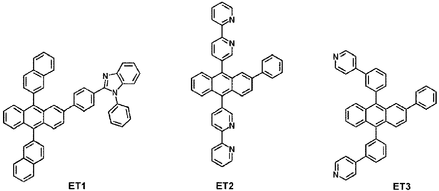

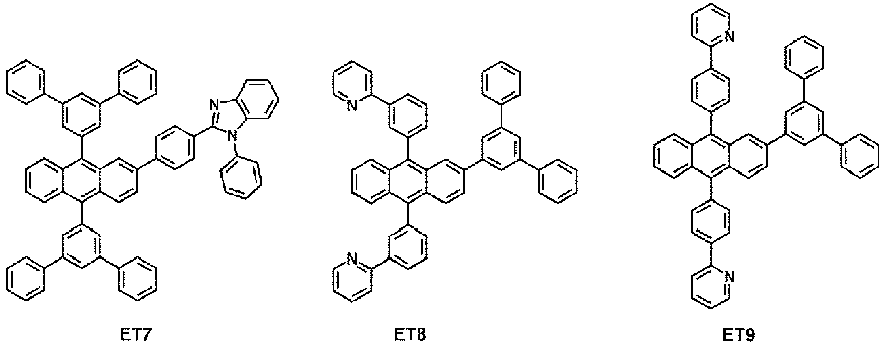


- In one or more embodiments, the electron transport region may include at least one selected from 2,9-dimethyl-4,7-diphenyl-1,10-phenanthroline (BCP), 4,7-dphenyl-1,10-phenanthroline (Bphen), Alq3, BAlq, 3-(biphenyl-4-yl)-5-(4-tert-butylphenyl)-4-phenyl-4H-1,2,4-triazole (TAZ), and NTAZ:


- Thicknesses of the buffer layer, the hole blocking layer, and the electron control layer may each independently be in a range of about 20 Å to about 1,000 Å, for example, about 30 Å to about 300 Å. When the thicknesses of the buffer layer, the hole blocking layer, and the electron control layer are within these ranges, excellent hole blocking characteristics or excellent electron control characteristics may be obtained without a substantial increase in driving voltage.
- A thickness of the electron transport layer may be in a range of about 100 Å to about 1,000 Å, for example, about 150 Å to about 500 Å. When the thickness of the electron transport layer is within the range described above, the electron transport layer may have satisfactory electron transport characteristics without a substantial increase in driving voltage.
- The electron transport region 17 (for example, the electron transport layer in the electron transport region) may further include, in addition to the materials described above, a metal-containing material.
- The metal-containing material may include at least one selected from alkali metal complex and alkaline earth-metal complex. The alkali metal complex may include a metal ion selected from a Li ion, a Na ion, a K ion, a Rb ion, and a Cs ion, and the alkaline earth-metal complex may include a metal ion selected from a Be ion, a Mg ion, a Ca ion, a Sr ion, and a Ba ion. A ligand coordinated with the metal ion of the alkali metal complex or the alkaline earth-metal complex may be selected from a hydroxy quinoline, a hydroxy isoquinoline, a hydroxy benzoquinoline, a hydroxy acridine, a hydroxy phenanthridine, a hydroxy phenyloxazole, a hydroxy phenylthiazole, a hydroxy diphenyloxadiazole, a hydroxy diphenylthiadiazole, a hydroxy phenylpyridine, a hydroxy phenylbenzimidazole, a hydroxy phenylbenzothiazole, a bipyridine, a phenanthroline, and a cyclopentadiene, but embodiments of the present disclosure are not limited thereto.
- For example, the metal-containing material may include a Li complex. The Li complex may include, for example, Compound ET-D1 (lithium quinolate, LiQ) or ET-D2:

- The
electron transport region 17 may include an electron injection layer that facilitates injection of electrons from thesecond electrode 19. The electron injection layer may directly contact thesecond electrode 19. - The electron injection layer may have i) a single-layered structure including a single layer including a single material, ii) a single-layered structure including a single layer including a plurality of different materials, or iii) a multi-layered structure having a plurality of layers including a plurality of different materials.
- The electron injection layer may include an alkali metal, an alkaline earth metal, a rare earth metal, an alkali metal compound, an alkaline earth-metal compound, a rare earth metal compound, an alkali metal complex, an alkaline earth-metal complex, a rare earth metal complex, or any combinations thereof.
- The alkali metal may be selected from Li, Na, K, Rb, and Cs. In one embodiment, the alkali metal may be Li, Na, or Cs. In one or more embodiments, the alkali metal may be Li or Cs, but embodiments of the present disclosure are not limited thereto.
- The alkaline earth metal may be selected from Mg, Ca, Sr, and Ba.
- The rare earth metal may be selected from Sc, Y, Ce, Tb, Yb, and Gd.
- The alkali metal compound, the alkaline earth-metal compound, and the rare earth metal compound may be selected from oxides and halides (for example, fluorides, chlorides, bromides, or iodides) of the alkali metal, the alkaline earth-metal, and the rare earth metal.
- The alkali metal compound may be selected from alkali metal oxides, such as Li2O, Cs2O, or K2O, and alkali metal halides, such as LiF, NaF, CsF, KF, LiI NaI, CsI or KI In one embodiment, the alkali metal compound may be selected from LiF, Li2O, NaF, LiI NaI CsI and KI but embodiments of the present disclosure are not limited thereto.
- The alkaline earth-metal compound may be selected from alkaline earth-metal oxides, such as BaO, SrO, CaO, BaxSr1-xO (0<x<1), or BaxCa1-xO (0<x<1). In one embodiment, the alkaline earth-metal compound may be selected from BaO, SrO, and CaO, but embodiments of the present disclosure are not limited thereto.
- The rare earth metal compound may be selected from YbF3, ScF3, ScO3, SC2O3, Y2O3, Ce2O3, GdF3, and TbF3. In one embodiment, the rare earth metal compound may be selected from YbF3, ScF3, TbF3, YbI3, ScI3, and TbI3, but embodiments of the present disclosure are not limited thereto.
- The alkali metal complex, the alkaline earth-metal complex, and the rare earth metal complex may include an ion of alkali metal, alkaline earth-metal, and rare earth metal as described above, and a ligand coordinated with a metal ion of the alkali metal complex, the alkaline earth-metal complex, or the rare earth metal complex may be selected from hydroxy quinoline, hydroxy isoquinoline, hydroxy benzoquinoline, hydroxy acridine, hydroxy phenanthridine, hydroxy phenyloxazole, hydroxy phenylthiazole, hydroxy diphenyloxadiazole, hydroxy diphenylthiadiazole, hydroxy phenylpyridine, hydroxy phenylbenzimidazole, hydroxy phenylbenzothiazole, bipyridine, phenanthroline, and cyclopentadiene, but embodiments of the present disclosure are not limited thereto.
- The electron injection layer may consist of an alkali metal, an alkaline earth metal, a rare earth metal, an alkali metal compound, an alkaline earth-metal compound, a rare earth metal compound, an alkali metal complex, an alkaline earth-metal complex, a rare earth metal complex, or any combinations thereof, as described above. In one or more embodiments, the electron injection layer may further include an organic material. When the electron injection layer further includes an organic material, an alkali metal, an alkaline earth metal, a rare earth metal, an alkali metal compound, an alkaline earth-metal compound, a rare earth metal compound, an alkali metal complex, an alkaline earth-metal complex, a rare earth metal complex, or any combinations thereof may be homogeneously or non-homogeneously dispersed in a matrix including the organic material.
- A thickness of the electron injection layer may be in a range of about 1 Å to about 100 Å, for example, about 3 Å to about 90 Å. When the thickness of the electron injection layer is within the range described above, the electron injection layer may have satisfactory electron injection characteristics without a substantial increase in driving voltage.
- The
second electrode 19 is located on theorganic layer 10A having such a structure. Thesecond electrode 19 may be a cathode which is an electron injection electrode, and in this regard, a material for forming thesecond electrode 19 may be selected from a metal, an alloy, an electrically conductive compound, and a combination thereof, which have a relatively low work function. - The
second electrode 19 may include at least one selected from lithium (Li), silver (Ag), magnesium (Mg), aluminum (Al), aluminum-lithium (Al-Li), calcium (Ca), magnesium-indium (Mg-In), magnesium-silver (Mg-Ag), ITO, and IZO, but embodiments of the present disclosure are not limited thereto. Thesecond electrode 19 may be a transmissive electrode, a semi-transmissive electrode, or a reflective electrode. - The
second electrode 19 may have a single-layered structure having a single layer or a multi-layered structure including two or more layers. - Hereinbefore, the organic light-emitting device has been described with reference to FIGURE, but embodiments of the present disclosure are not limited thereto.
-
FIG. 3 is a schematic cross-sectional view of an organic light-emittingdevice 100 according to another embodiment. - The organic light-emitting
device 100 ofFIG. 3 includes afirst electrode 110, asecond electrode 190 facing thefirst electrode 110, and afirst emission unit 151 and asecond emission unit 152 between thefirst electrode 110 and thesecond electrode 190. Acharge generating layer 141 is located between thefirst emission unit 151 and thesecond emission unit 152, and thecharge generating layer 141 may include an n-type charge generating layer 141-N and a p-type charge generating layer 141-P. Thecharge generating layer 141 is a layer that generates charge and supplies the charge to neighboring emission units, and any known material may be used therefor. - The
first emission unit 151 may include a first emission layer 151-EM, and thesecond emission unit 152 may include a second emission layer 152-EM. The maximum emission wavelength of light emitted from thefirst emission unit 151 may be different from the maximum emission wavelength of light emitted from thesecond emission unit 152. For example, the mixed light of the light emitted from thefirst emission unit 151 and the light emitted from thesecond emission unit 152 may be white light, but embodiments of the present disclosure are not limited thereto. - The
hole transport region 120 is located between thefirst emission unit 151 and thefirst electrode 110, and thesecond emission unit 152 may include the firsthole transport region 121 located on the side of thefirst electrode 110 . - An
electron transport region 170 is located between thesecond emission unit 152 and thesecond electrode 190, and thefirst emission unit 151 may include a firstelectron transport region 171 located between thecharge generating layer 141 and the first emission layer 151-EM. - The first emission layer 151-EM may include a host, a cooling dopant, and a sensitizer, and the cooling dopant and the sensitizer may satisfy
Conditions - The second emission layer 152-EM may include a host, a cooling dopant, and a sensitizer, and the cooling dopant and the sensitizer may satisfy
Conditions - The
first electrode 110 and thesecond electrode 190 illustrated inFIG. 3 may be the same as described in connection with thefirst electrode 11 and thesecond electrode 19 illustrated inFIG. 1 . - The first emission layer 151-EM and the second emission layer 152-EM illustrated in
FIG. 3 are each the same as described in connection with theemission layer 15 illustrated inFIG. 1 . - The
hole transport region 120 and the firsthole transport region 121 illustrated inFIG. 3 are each the same as described in connection with thehole transport region 12 illustrated inFIG. 1 . - The
electron transport region 170 and the firstelectron transport region 171 illustrated inFIG. 3 are each the same as described in connection with theelectron transport region 17 illustrated inFIG. 1 . - As described above, referring to
FIG. 3 , an organic light-emitting device in which each of thefirst emission unit 151 and thesecond emission unit 152 includes an emission layer including a host, a cooling dopant, and a sensitizer, has been described. However, the organic light-emitting device may have various other forms. For example, one of thefirst emission unit 151 and thesecond emission unit 152 of the organic light-emittingdevice 100 ofFIG. 3 may be replaced with any known emission unit, or may include three or more emission units. -
FIG. 4 is a schematic cross-sectional view of an organic light-emittingdevice 200 according to another embodiment. - The organic light-emitting
device 200 includes afirst electrode 210, asecond electrode 290 facing thefirst electrode 210, and afirst emission layer 251 and asecond emission layer 252 which are stacked between thefirst electrode 210 and thesecond electrode 290. - The maximum emission wavelength of light emitted from the
first emission layer 251 may be different from the maximum emission wavelength of light emitted from thesecond emission layer 252. For example, the mixed light of the light emitted from thefirst emission layer 251 and the light emitted from thesecond emission layer 252 may be white light, but embodiments of the present disclosure are not limited thereto. - In one or more embodiments, a
hole transport region 220 may be located between thefirst emission layer 251 and thefirst electrode 210, and anelectron transport region 270 may be located between thesecond emission layer 252 and thesecond electrode 290. - The
first emission layer 251 may include a host, a cooling dopant, and a sensitizer, and the cooling dopant and the sensitizer may satisfyConditions - The
second emission layer 252 may include a host, a cooling dopant, and a sensitizer, and the cooling dopant and the sensitizer may satisfyConditions - The
first electrode 210, thehole transport region 220, and thesecond electrode 290 illustrated inFIG. 4 are respectively the same as described in connection with thefirst electrode 11, thehole transport region 12, and thesecond electrode 19 illustrated inFIG. 1 . - The
first emission layer 251 and thesecond emission layer 252 illustrated inFIG. 4 are each the same as described in connection with theemission layer 15 illustrated inFIG. 1 . - The
electron transport region 270 illustrated inFIG. 4 may be the same as described in connection with theelectron transport region 17 inFIG. 1 . - As described above, referring to
FIG. 4 , an organic light-emitting device, in which each of thefirst emission layer 251 and thesecond emission layer 252 includes a host, a cooling dopant, and a sensitizer, has been described. However, the organic light-emitting device may have various other forms. For example, one of thefirst emission layer 251 and thesecond emission layer 252 of the organic light-emittingdevice 200 ofFIG. 4 may be replaced with any known emission layer, or an interlayer may be additionally located between neighboring emission layers. - The term "C1-C60 alkyl group" as used herein refers to a linear or branched saturated aliphatic hydrocarbon monovalent group having 1 to 60 carbon atoms, and examples thereof include a methyl group, an ethyl group, a propyl group, an isobutyl group, a sec-butyl group, a tert-butyl group, a pentyl group, an isoamyl group, and a hexyl group. The term "C1-C60 alkylene group" as used herein refers to a divalent group having the same structure as the C1-C60 alkyl group.
- The term "C1-C60 alkoxy group" used herein refers to a monovalent group represented by -OA101 (wherein A101 is the C1-C60 alkyl group), and examples thereof include a methoxy group, an ethoxy group, and an isopropyloxy group.
- The term "C2-C60 alkenyl group" as used herein refers to a hydrocarbon group formed by substituting at least one carbon-carbon double bond in the middle or at the terminus of the C2-C60 alkyl group, and examples thereof include an ethenyl group, a propenyl group, and a butenyl group. The term "C2-C60 alkenylene group" as used herein refers to a divalent group having the same structure as the C2-C60 alkenyl group.
- The term "C2-C60 alkynyl group" as used herein refers to a hydrocarbon group formed by substituting at least one carbon-carbon triple bond in the middle or at the terminus of the C2-C60 alkyl group, and examples thereof include an ethynyl group, and a propynyl group. The term "C2-C60 alkynylene group" as used herein refers to a divalent group having the same structure as the C2-C60 alkynyl group.
- The term "C3-C10 cycloalkyl group" as used herein refers to a monovalent saturated hydrocarbon monocyclic group having 3 to 10 carbon atoms, and examples thereof include a cyclopropyl group, a cyclobutyl group, a cyclopentyl group, a cyclohexyl group, and a cycloheptyl group. The term "C3-C10 cycloalkylene group" as used herein refers to a divalent group having the same structure as the C3-C10 cycloalkyl group.
- The term "C1-C10 heterocycloalkyl group" as used herein refers to a monovalent saturated monocyclic group having at least one heteroatom selected from N, O, P, Si, and S as a ring-forming atom and 1 to 10 carbon atoms, and non-limiting examples thereof include a tetrahydrofuranyl group, and a tetrahydrothiophenyl group. The term "C1-C10 heterocycloalkylene group" as used herein refers to a divalent group having the same structure as the C1-C10 heterocycloalkyl group.
- The term "C3-C10 cycloalkenyl group" as used herein refers to a monovalent monocyclic group that has 3 to 10 carbon atoms and at least one carbon-carbon double bond in the ring thereof and no aromaticity, and non-limiting examples thereof include a cyclopentenyl group, a cyclohexenyl group, and a cycloheptenyl group. The term "C3-C10 cycloalkenylene group" as used herein refers to a divalent group having the same structure as the C3-C10 cycloalkenyl group.
- The term "C1-C10 heterocycloalkenyl group" as used herein refers to a monovalent monocyclic group that has at least one heteroatom selected from N, O, P, Si, and S as a ring-forming atom, 1 to 10 carbon atoms, and at least one carbon-carbon double bond in its ring. Examples of the C1-C10 heterocycloalkenyl group are a 2,3-dihydrofuranyl group, and a 2,3-dihydrothiophenyl group. The term "C1-C10 heterocycloalkenylene group" as used herein refers to a divalent group having the same structure as the C1-C10 heterocycloalkenyl group.
- The term "C6-C60 aryl group" as used herein refers to a monovalent group having a carbocyclic aromatic system having 6 to 60 carbon atoms, and the term "C6-C60 arylene group" as used herein refers to a divalent group having a carbocyclic aromatic system having 6 to 60 carbon atoms. Examples of the C6-C60 aryl group include a phenyl group, a naphthyl group, an anthracenyl group, a phenanthrenyl group, a pyrenyl group, and a chrysenyl group. When the C6-C60 aryl group and the C6-C60 arylene group each include two or more rings, the rings may be fused to each other.
- The term "C1-C60 heteroaryl group" as used herein refers to a monovalent group having a heterocarbocyclic aromatic system that has at least one heteroatom selected from N, O, P, Si, and S as a ring-forming atom, and 1 to 60 carbon atoms. The term "C1-C60 heteroarylene group" as used herein refers to a divalent group having a carbocyclic aromatic system that has at least one heteroatom selected from N, O, P, and S as a ring-forming atom, and 1 to 60 carbon atoms. Examples of the C1-C60 heteroaryl group include a pyridinyl group, a pyrimidinyl group, a pyrazinyl group, a pyridazinyl group, a triazinyl group, a quinolinyl group, and an isoquinolinyl group. When the C6-C60 heteroaryl group and the C6-C60 heteroarylene group each include two or more rings, the rings may be fused to each other.
- The term "C6-C60 aryloxy group" as used herein refers to -OA102 (wherein A102 is the C6-C60 aryl group), and a C6-C60 arylthio group used herein refers to -SA103 (wherein A103 is the C6-C60 aryl group).
- The term "monovalent non-aromatic condensed polycyclic group" used herein refers to a monovalent group in which two or more rings are condensed with each other, only carbon is used as a ring-forming atom (for example, the number of carbon atoms may be 8 to 60) and the whole molecule is a non-aromaticity group. Examples of the monovalent non-aromatic condensed polycyclic group include a fluorenyl group. The term "divalent non-aromatic condensed polycyclic group" as used herein refers to a divalent group having the same structure as the monovalent non-aromatic condensed polycyclic group.
- The term "monovalent non-aromatic condensed heteropolycyclic group" as used herein refers to a monovalent group having two or more rings condensed to each other, a heteroatom selected from N, O, P, Si, and S, other than carbon atoms(for example, having 1 to 60 carbon atoms), as a ring-forming atom, and no aromaticity in its entire molecular structure. Examples of the monovalent non-aromatic condensed heteropolycyclic group include a carbazolyl group. The term "divalent non-aromatic condensed heteropolycyclic group" as used herein refers to a divalent group having the same structure as the monovalent non-aromatic condensed heteropolycyclic group.
- The term "C5-C30 carbocyclic group" as used herein refers to a saturated or unsaturated cyclic group having, as a ring-forming atom, 5 to 30 carbon atoms only. The C5-C30 carbocyclic group may be a monocyclic group or a polycyclic group, and may be a monovalent, divalent, trivalent, tetravalent, pentavalent, or hexavalent group, depending on the formula structure.
- The term "C1-C30 heterocyclic group" as used herein refers to a saturated or unsaturated cyclic group having, as a ring-forming atom, at least one heteroatom selected from N, O, Si, P, and S other than 1 to 30 carbon atoms. The C1-C30 heterocyclic group may be a monocyclic group or a polycyclic group, and may be a monovalent, divalent, trivalent, tetravalent, pentavalent, or hexavalent group, depending on the formula structure.
- At least one substituent of the substituted C5-C60 carbocyclic group, the substituted C1-C60 heterocyclic group, the substituted C1-C60 alkyl group, the substituted C2-C60 alkenyl group, the substituted C2-C60 alkynyl group, the substituted C1-C60 alkoxy group, the substituted C3-C10 cycloalkyl group, the substituted C1-C10 heterocycloalkyl group, the substituted C3-C10 cycloalkenyl group, the substituted C1-C10 heterocycloalkenyl group, the substituted C6-C60 aryl group, the substituted C6-C60 aryloxy group, the substituted C6-C60 arylthio group, the substituted C1-C60 heteroaryl group, the substituted monovalent non-aromatic condensed polycyclic group, and the substituted monovalent non-aromatic condensed heteropolycyclic group may be selected from:
- deuterium, -F, -Cl, -Br, -I, -CD3, -CD2H, -CDH2, -CF3, -CF2H, -CFH2, a hydroxyl group, a cyano group, a nitro group, an amino group, an amidino group, a hydrazine group, a hydrazone group, a carboxylic acid or a salt thereof, a sulfonic acid or a salt thereof, a phosphoric acid or a salt thereof, a C1-C60 alkyl group, a C2-C60 alkenyl group, a C2-C60 alkynyl group, and a C1-C60 alkoxy group;
- a C1-C60 alkyl group, a C2-C60 alkenyl group, a C2-C60 alkynyl group, and a C1-C60 alkoxy group, each substituted with at least one of deuterium, -F, -Cl, -Br, -I, -CD3, -CD2H, -CDH2, -CF3, -CF2H, -CFH2, a hydroxyl group, a cyano group, a nitro group, an amino group, an amidino group, a hydrazine group, a hydrazone group, a carboxylic acid or a salt thereof, a sulfonic acid or a salt thereof, a phosphoric acid or a salt thereof, a C3-C10 cycloalkyl group, a C1-C10 heterocycloalkyl group, a C3-C10 cycloalkenyl group, a C1-C10 heterocycloalkenyl group, a C6-C60 aryl group, a C6-C60 aryloxy group, a C6-C60 arylthio group, a C1-C60 heteroaryl group, a monovalent non-aromatic condensed polycyclic group, a monovalent non-aromatic condensed heteropolycyclic group, -N(Q11)(Q12), -Si(Q13)(Q14)(Q15), -B(Q16)(Q17), and -P(=O)(Q18)(Q19);
- a C3-C10 cycloalkyl group, a C1-C10 heterocycloalkyl group, a C3-C10 cycloalkenyl group, a C1-C10 heterocycloalkenyl group, a C6-C60 aryl group, a C6-C60 aryloxy group, a C6-C60 arylthio group, a C1-C60 heteroaryl group, a monovalent non-aromatic condensed polycyclic group, and a monovalent non-aromatic condensed heteropolycyclic group;
- a C3-C10 cycloalkyl group, a C1-C10 heterocycloalkyl group, a C3-C10 cycloalkenyl group, a C1-C10 heterocycloalkenyl group, a C6-C60 aryl group, a C6-C60 aryloxy group, a C6-C60 arylthio group, a C1-C60 heteroaryl group, a monovalent non-aromatic condensed polycyclic group, and a monovalent non-aromatic condensed heteropolycyclic group, each substituted with at least one of deuterium, -F, -Cl, -Br, -I, -CD3, -CD2H, -CDH2, -CF3, -CF2H, -CFH2, a hydroxyl group, a cyano group, a nitro group, an amidino group, a hydrazine group, a hydrazone group, a carboxylic acid or a salt thereof, a sulfonic acid or a salt thereof, a phosphoric acid or a salt thereof, a C1-C60 alkyl group, a C2-C60 alkenyl group, a C2-C60 alkynyl group, a C1-C60 alkoxy group, a C3-C10 cycloalkyl group, a C1-C10 heterocycloalkyl group, a C3-C10 cycloalkenyl group, a C1-C10 heterocycloalkenyl group, a C6-C60 aryl group, a C6-C60 aryloxy group, a C6-C60 arylthio group, a C1-C60 heteroaryl group, a monovalent non-aromatic condensed polycyclic group, a monovalent non-aromatic condensed heteropolycyclic group, -N(Q21)(Q22), -Si(Q23)(Q24)(Q25), -B(Q26)(Q27), and -P(=O)(Q28)(Q29); and
- -N(Q31)(Q32), -Si(Q33)(Q34)(Q35), -B(Q36)(Q37), and -P(=O)(Q38)(Q39),
- wherein Q1 to Q9, Q11 to Q19, Q21 to Q29 and Q31 to Q39 may each independently be selected from hydrogen, deuterium, -F, -Cl, -Br, -I, a hydroxyl group, a cyano group, a nitro group, an amino group, an amidino group, a hydrazine group, a hydrazone group, a carboxylic acid or a salt thereof, a sulfonic acid or a salt thereof, a phosphoric acid or a salt thereof, a C1-C60 alkyl group, a C2-C60 alkenyl group, a C2-C60 alkynyl group, a C1-C60 alkoxy group, a C3-C10 cycloalkyl group, a C1-C10 heterocycloalkyl group, a C3-C10 cycloalkenyl group, a C1-C10heterocycloalkenyl group, a C6-C60 aryl group, a C6-C60 aryl group substituted with at least one selected from a C1-C60 alkyl group, and a C6-C60 aryl group, a C6-C60 aryloxy group, a C6-C60 arylthio group, a C1-C60 heteroaryl group, a monovalent non-aromatic condensed polycyclic group, and a monovalent non-aromatic condensed heteropolycyclic group.
- The term "room temperature" used herein refers to a temperature of about 25°C.
- The terms "a biphenyl group, a terphenyl group, and a tetraphenyl group" used herein respectively refer to monovalent groups in which two, three, or four phenyl groups which are linked together via a single bond.
- The terms "a cyano-containing phenyl group, a cyano-containing biphenyl group, a cyano-containing terphenyl group, and a cyano-containing tetraphenyl group" used herein respectively refer to a phenyl group, a biphenyl group, a terphenyl group, and a tetraphenyl group, each of which is substituted with at least one cyano group. In "a cyano-containing phenyl group, a cyano-containing biphenyl group, a cyano-containing terphenyl group, and a cyano-containing tetraphenyl group", a cyano group may be substituted to any position of the corresponding group, and the "cyano-containing phenyl group, the cyano-containing biphenyl group, the cyano-containing terphenyl group, and the cyano-containing tetraphenyl group" may further include substituents other than a cyano group. For example, a phenyl group substituted with a cyano group, and a phenyl group substituted with a cyano group and a methyl group may all belong to "a cyano-containing phenyl group."
- Hereinafter, a compound and an organic light-emitting device according to embodiments are described in detail with reference to Synthesis Examples and Examples. However, the organic light-emitting device is not limited thereto. The wording "'B' was used instead of 'A''' used in describing Synthesis Examples means that an amount of 'A' used was identical to an amount of 'B' used, in terms of a molar equivalent.
- On the quartz substrate, compounds of Tables 5 to 7 were vacuum-codeposited at a vacuum degree of 10-7 torr at a weight ratio of Tables 5 to 7 to manufacture films, each having a thickness of 40 nm. With respect to each of the films, the PL spectrum was evaluated at room temperature by using
FluoTime 300 of PicoQuant Inc. and PLS340, which is a pumping source of PicoQuant Inc., (excitation wavelength = 340 nm, and spectrum width = 20 nm). In detail, the wavelength of the main peak of the spectrum obtained for each film was identified, and the number of photons emitted from the respective sample at the wavelength of the main peak by photon pulses (pulse width = 500 ps) applied by the PLS340 to the respective film was repeatedly measured based on time-correlated single photon counting (TCSPC), to obtain a TRPL curve which can be subjected to fitting. Two or more exponential decay functions, obtained therefrom, were subjected to fitting to calculate a decay time with respect to each film. In this regard, the same measurement was performed for the same measurement time as used to obtain the TRPL curve in the dark condition (The light low pulse signal incident to the predetermined film was blocked) to obtain a background signal curve which was then subjected to fitting. The resultant was used as a baseline. - At this time, in the case of the film of Table 5, the function used for fitting is the same as Equation A below, and the largest value among the Taus obtained therefrom was taken. For the films of Tables 6 and 7 below, Tau was obtained by <Equation B> using the amplitude values (A1, A2, A3, etc.) and Tau values (Tau1, Tau2, Tau3, etc.) obtained by fitting:


[Table 5] Film No. Film composition (weight ratio) Decay time(µs) SP002ND H-H1 : H-E1 : SP002 (45 : 45 : 10) 2.393 SP003ND H-H1 : H-E1 : SP003 (45 : 45 : 10) 2.703 SP004ND H-H1 : H-E1 : SP004 (45 : 45 : 10) 4.924 SP005ND H-H1 : H-E1 : SP005 (45 : 45 : 10) 2.866 SP006ND H-H1 : H-E1 : SP006 (45 : 45 : 10) 1.836 SP007ND H-H1 : H-E1 : SP007 (45 : 45 : 10) 2.223 ST001 ND H-H1 : H-E1 : ST001 (45 : 45 : 10) 1.13 ST002ND H-H1 : H-E1 : ST002 (45 : 45 : 10) 2.69 Table 6 Film No. Film composition (weight ratio) Decay time(µs) SP002D H-H1 : H-E1 : SP002 : FD11 (42.75 : 42.75 : 9.5 : 5) 0.363 SP003D H-H1 : H-E1 : SP003 : FD11 (42.75 : 42.75 : 9.5 : 5) 0.378 SP004D H-H1 : H-E1 : SP004 : FD11 (42.75 : 42.75 : 9.5 : 5) 0.269 SP005D H-H1 : H-E1 : SP005 : FD11 (42.75 : 42.75 : 9.5 : 5) 0.398 SP006D1 H-H1 : H-E1 : SP006 : FD11 (42.75 : 42.75 : 9.5 : 5) 0.307 SP006D2 H-H1 : H-E1 : SP006 : FD5 (42.75 : 42.75 : 9.5 : 5) 0.634 SP007D1 H-H1 : H-E1 : SP007 : FD11 (42.75 : 42.75 : 9.5 : 5) 0.413 SP007D2 H-H1 : H-E1 : SP007 : FD5 (42.75 : 42.75 : 9.5 : 5) 0.749 ST001 D1 H-H1 : H-E1 : ST001 : FD11 (42.75 : 42.75 : 9.5 : 5) 0.012 ST001 D2 H-H1 : H-E1 : ST001 : FD5 (42.75 : 42.75 : 9.5 : 5) 0.09 ST002D1 H-H1 : H-E1 : ST002 : FD11 (42.75 : 42.75 : 9.5 : 5) 0.719 ST002D2 H-H1 : H-E1 : ST002 : FD5 (42.75 : 42.75 : 9.5 : 5) 0.673 Table 7 Film No. Film composition (weight ratio) Decay time(µs) FD001 H-H1 : H-E1 : FD11 (47.5 : 47.5 : 5) 0.027 FD002 H-H1 : H-E1 : FD5 (47.5 : 47.5 : 5) 0.069 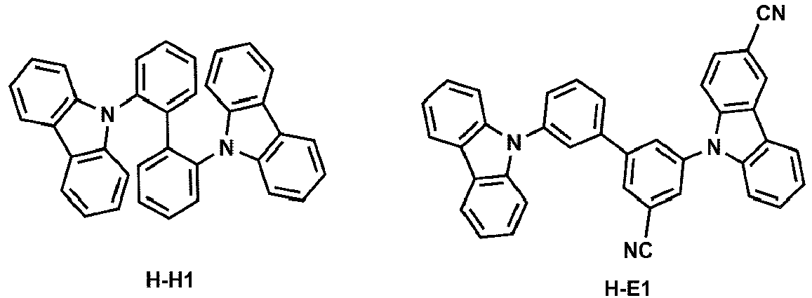


- An ITO glass substrate was cut to a size of 50 mm x 50 mm x 0.5 mm and then, sonicated in acetone isopropyl alcohol and pure water, each for 15 minutes, and then, washed by exposure to UV ozone for 30 minutes.
- Then, F6-TCNNQ was deposited on the ITO electrode (anode) of the glass substrate to form a hole injection layer having a thickness of 100Å, and HT1 was deposited on the hole injection layer to form a hole transport layer having a thickness of 1260 Å, thereby completing a hole transport region.
- Compound H-H1 (first host), H-E1 (second host), Compound SP002(sensitizer)(in this case, the weight ratio of the first host, the second host and the sensitizer was 45:45:10) and FD11 (cooling dopant)(in this case, the cooling dopant was 5 wt% based on the total weight of the first host, the second host, the sensitizer, and the cooling dopant) were co-deposited on the hole transport region to form an emission layer having a thickness of 400Å thickness.
- Compound ET17 and Liq were co-deposited at the weight ratio of 5:5 on the emission layer to form an electron transport layer having a thickness of 360Å thickness, and then, LiQ was deposited on the electron transport layer to form an electron injection layer having a thickness of 5Å thickness, and Al was deposited on the electron injection layer to a thickness of 800Å, thereby completing of an organic light-emitting device.
- Organic light-emitting devices were manufactured in the same manner as in Example 1, except that the sensitizers and the cooling dopants shown in Table 8 were used in forming an emission layer.
Table 8 First host Second host Sensitizer Cooling dopant Example 1 H-H1 H-E1 SP002 FD11 Example 2 H-H1 H-E1 SP003 FD11 Example 3 H-H1 H-E1 SP004 FD11 Example 4 H-H1 H-E1 SP005 FD11 Example 5 H-H1 H-E1 SP006 FD11 Example 6 H-H1 H-E1 SP006 FD5 Example 7 H-H1 H-E1 SP007 FD11 Example 8 H-H1 H-E1 SP007 FD5 Example 9 H-H1 H-E1 ST001 FD11 Example 10 H-H1 H-E1 ST001 FD5 Example 11 H-H1 H-E1 ST002 FD11 Example 12 H-H1 H-E1 ST002 FD5 - Organic light-emitting devices were manufactured in the same manner as in Example 1, except that, in forming an emission layer, a sensitizer was not used and the first host, the second host, and the cooling dopant were used as shown in Table 9.
Table 9 First host Second host Cooling dopant Weight ratio (first host: second host: cooling dopant) Comparative Example 1F H-H1 H-E1 FD11 47.5 : 47.5 : 5 Comparative Example 2F H-H1 H-E1 FD5 47.5 : 47.5 : 5 - Organic light-emitting devices were manufactured in the same manner as in Example 1, except that, in forming an emission layer, a cooling dopant was not used and the first host, the second host, and the sensitizer were used as shown in Table 10.
Table 10 First host Second host Sensitizer Weight ratio (first host: second host: sensitizer) Comparative Example 1P H-H1 H-E1 SP002 45 : 45 : 10 Comparative Example 2P H-H1 H-E1 SP003 45 : 45 : 10 Comparative Example 3P H-H1 H-E1 SP004 45 : 45 : 10 Comparative Example 4P H-H1 H-E1 SP005 45 : 45 : 10 Comparative Example 5P H-H1 H-E1 SP006 45 : 45 : 10 Comparative Example 6P H-H1 H-E1 SP007 45 : 45 : 10 - Organic light-emitting devices were manufactured in the same manner as in Example 1, except that, in forming an emission layer, a cooling dopant was not used and the first host, the second host, and the sensitizer were used as shown in Table 11.
Table 11 First host Second host Sensitizer Weight ratio (first host: second host: sensitizer) Comparative Example 1T H-H1 H-E1 ST001 45 : 45 : 10 Comparative Example 2T H-H1 H-E1 ST002 45 : 45 : 10 - The external quantum efficiency (EQE) and lifespan of each of organic light-emitting devices manufactured according to Examples 1 to 12 were evaluated, and then, the results are calculated as a relative value (%), and results thereof are shown in Table 12. As an evaluation apparatus, a luminance meter (Minolta Cs-1000A) was used. The lifespan (T95) was determined by evaluating the time taken for 100% of initial luminance to be 95% thereof under the same luminance measurement conditions.
- In addition, after measuring the lifespan and EQE of Example 3, Comparative Example 3P, 1F, and 2F, the relative value (%) was calculated based on the value of Comparative Example 1F and the results are shown in Table 13, and
FIGS. 5 and 6 .Table 12 First host Second host Sensitizer Cooling dopant Lifespan (%) EQE (%) Example 1 H-H1 H-E1 SP002 FD11 688 181 Example 2 H-H1 H-E1 SP003 FD11 234 142 Example 3 H-H1 H-E1 SP004 FD11 296 121 Example 4 H-H1 H- E1 SP005 FD11 100 100 Example 5 H-H1 H-E1 SP006 FD11 1051 134 Example 6 H-H1 H-E1 SP006 FD5 340 102 Example 7 H-H1 H-E1 SP007 FD11 1355 144 Example 8 H-H1 H-E1 SP007 FD5 487 124 Example 9 H-H1 H-E1 ST001 FD11 43 65 Example 10 H-H1 H-E1 ST001 FD5 24 86 Example 11 H-H1 H-E1 ST002 FD11 232 129 Example 12 H-H1 H-E1 ST002 FD5 140 162 - Referring to Table 12, it can be seen that the organic light-emitting device of Example 1 to 12 has long life span and high efficiency.
Table 13 First host Second host Sensitizer Cooling dopant Lifespan (%) EQE (%) Example 3 H-H1 H-E1 SP004 FD11 296 121 Comparative Example 3P H-H1 H-E1 SP004 - 13 86 Comparative Example 1F H-H1 H-E1 - FD11 66 31 - Referring to Table 13, and
FIGS. 5 and 6 , it can be seen that the organic light-emitting device of Example 3 has a long lifespan and high EQE compared to a phosphorescent organic light-emitting device (Comparative Example 3P) and a fluorescent organic light-emitting device (Comparative Example 1F). - For Examples 1 to 12 and Comparative Examples 1F and 2F, the time (T95) taken for 100% of the initial luminance to be decreased to 95% thereof at 6000 nits was measured. Then, the lifespan increase of Example 1 to 12 was calculated using the following equation L and the results are shown in Table 14.

Table 14 Device A Device B Lifespan Increase of Device A Example 1 Comparative Example 1F 5.8 Example 2 Comparative Example 1F 4.6 Example 3 Comparative Example 1F 22.3 Example 4 Comparative Example 1F 9.74 Example 5 Comparative Example 1F 5.70 Example 6 Comparative Example 2F 1.84 Example 7 Comparative Example 1F 4.17 Example 8 Comparative Example 2F 1.5 Example 9 Comparative Example 1F 11.3 Example 10 Comparative Example 2F 6.14 Example 11 Comparative Example 1F 5.74 Example 12 Comparative Example 2F 3.46 - Referring to the Table 14, it can be seen that the organic light-emitting devices of Examples 1 to 12 have a significant improvement in lifespan compared to the fluorescent organic light-emitting devices of Comparative Examples 1F and 2F which do not include the sensitizer.
- For Examples 1 to 12, Comparative Examples 1P to 6P, and Comparative Examples 1T and 2T, external quantum efficiency (EQE) was measured. Then, the lifespan increase of Example 1 to 12 was calculated using the following equation E and the results are shown in Table 15.

Table 15 Device C Device D EQE increment of device C Example 1 Comparative Example 1P 5.78 Example 2 Comparative Example 2P 4.52 Example 3 Comparative Example 3P 3.85 Example 4 Comparative Example 4P 3.19 Example 5 Comparative Example 5P 4.26 Example 6 Comparative Example 5P 1.66 Example 7 Comparative Example 6P 4.60 Example 8 Comparative Example 6P 2.02 Example 9 Comparative Example 1T 2.07 Example 10 Comparative Example 1T 1.40 Example 11 Comparative Example 4.11 2T Example 12 Comparative Example 2T 2.62 - Referring to the Table 15, it can be seen that the organic light-emitting devices of Examples 1 to 12 show a significant improvement in EQE compared to Comparative Examples 1P to 6P which do not include a cooling dopant, phosphorescence of 1T, and 2T, or TADF organic light-emitting devices.
- The organic light-emitting device may have a long lifespan.
- It should be understood that embodiments described herein should be considered in a descriptive sense only and not for purposes of limitation. Descriptions of features or aspects within each embodiment should typically be considered as available for other similar features or aspects in other embodiments. While one or more embodiments have been described with reference to the figures, it will be understood by those of ordinary skill in the art that various changes in form and details may be made therein without departing from the scope as defined by the following claims.
<Formula H-1 > Ar401-(L401)xd1-(Ar402)xd11

L401 may be selected from:
Claims (15)
- An organic light-emitting device comprising:a first electrode; a second electrode; and an organic layer between the first electrode and the second electrode;the organic layer comprises an emission layer;the emission layer comprises a host, a cooling dopant, and a sensitizer, whereinthe cooling dopant and the sensitizer satisfy Conditions 1 and 2, andthe sensitizer comprises platinum (Pt):

 Tdecay(CD) is a decay time of the cooling dopant, andTdecay(S) is a decay time of the sensitizer.
 - An organic light-emitting device comprising:a first electrode; a second electrode; and an organic layer between the first electrode and the second electrode;the organic layer comprises an emission layer;the emission layer comprises a host, a cooling dopant, and a sensitizer, whereinthe cooling dopant and the sensitizer satisfy Conditions 1 and 2, andthe sensitizer comprises a thermally activated delayed fluorescence emitter, andthe thermally activated delayed fluorescence emitter does not include metal:

 Tdecay(CD) is a decay time of the cooling dopant, andTdecay(S) is a decay time of the sensitizer.
 - The organic light-emitting device of claim 1 or claim 2, wherein the organic light-emitting device further satisfies Condition 3:
 Tdecay(CD) is a decay time of the cooling dopant, andTdecay(S) is a decay time of the sensitizer; and/orwherein
the organic light-emitting device further satisfies Condition 4: BDE (S) is the bond dissociation energy level of the sensitizer, andT1 (S) is the lowest excitation triplet energy level of the sensitizer; and/orwherein
the organic light-emitting device further satisfies Condition 5:
R (Hex) is the production rate of hot excitons; and/or
wherein
the host, the dopant, and the sensitizer further satisfy Condition 6: T1(H) is the lowest excitation triplet energy level of the host,T1(S) is the lowest excitation triplet energy level of the sensitizer, andS1(CD) is the lowest excitation singlet energy level of the cooling dopant.
 - The organic light-emitting device of any of claims 1-3, wherein
the emission layer consists of the host, the cooling dopant, and the sensitizer. - The organic light-emitting device of any of claims 1-4, wherein
the host comprises an amphiprotic host, an electron transport host, and/or a hole transport host,
the electron transport host comprises at least one electron transport moiety, the hole transport host does not include an electron transport moiety,
the electron transport moiety is selected from a cyano group, a π electron-deficient nitrogen-containing cyclic group, and a group represented by one of the following Formulae:
- The organic light-emitting device of claim 5, wherein
the electron transport host comprises at least one π electron-deficient nitrogen-free cyclic group and at least one electron transport moiety,
the hole transport host comprises at least one π electron-deficient nitrogen-free cyclic group, and does not include an electron transport moiety, and
the electron transport moiety is a cyano group or an π-electron deficient nitrogen-containing cyclic group;
preferably wherein
the π electron-deficient nitrogen-containing cyclic group is selected from: an imidazole group, a pyrazole group, a thiazole group, an isothiazole group, an oxazole group, an isoxazole group, a pyridine group, a pyrazine group, a pyridazine group, a pyrimidine group, an indazole group, a purine group, a quinoline group, an isoquinoline group, a benzoquinoline group, a phthalazine group, a naphthyridine group, a quinoxaline group, a quinazoline group, a cinnoline group, a phenanthridine group, an acridine group, a phenanthroline group, a phenazine group, a benzimidazole group, an isobenzothiazole group, a benzoxazole group, an isobenzoxazole group, a triazole group, a tetrazole group, an oxadiazole group, a triazine group, a thiadiazole group, an imidazopyridine group, an imidazopyrimidine group, and an azacarbazole group; and a condensed cyclic group in which two or more π electron-deficient nitrogen-containing cyclic groups,
the π electron-deficient nitrogen-free cyclic group is selected from a benzene group, a heptalene group, an indene group, a naphthalene group, an azulene group, an indacene group, acenaphthylene group, a fluorene group, a spiro-bifluorene group, a benzofluorene group, a dibenzofluorene group, a phenalene group, a phenanthrene group, an anthracene group, a fluoranthene group, a triphenylene group, a pyrene group, a chrysene group, a naphthacene group, a picene group, a perylene group, a pentacene group, a hexacene group, a pentaphene group, a rubicene group, a coronene group, an ovalene group, a pyrrole group, an isoindole group, an indole group, a furan group, a thiophene group, a benzofuran group, a benzothiophene group, a benzocarbazole group, a dibenzocarbazole group, a dibenzofuran group, a dibenzothiophene group, a dibenzothiophene sulfone group, a carbazole group, a dibenzosilole group, an indenocarbazole group, an indolocarbazole group, a benzofurocarbazole group, a benzothienocarbazole group, a triindolobenzene group; and a condensed cyclic group of two or more π electron-deficient nitrogen-free cyclic groups. - The organic light-emitting device of claims 5 or 6, wherein
the electron transport host comprises i) at least one of a cyano group, a pyrimidine group, a pyrazine group, and a triazine group and ii) a triphenylene group, and
the hole transport host comprises a carbazole group. - The organic light-emitting device of any of claims 1-7, wherein the maximum emission wavelength of the emission spectrum of the cooling dopant is 400 nm or more and 550 nm or less; and/or
wherein the cooling dopant does not include a metal atom; and/or
wherein
the cooling dopant comprises one of a naphthalene-containing core, a fluorene-containing core, a spiro-bifluorene-containing core, a benzofluorene-containing core, a dibenzofluorene-containing core, a phenanthrene-containing core, an anthracene-containing core, a fluoranthene-containing core, a triphenylene-containing core, a pyrene-containing core, a chrysene-containing core, a naphthacene-containing core, a picene-containing core, a perylene-containing core, a pentaphene-containing core, an indenoanthracene-containing core, a bisanthracene-containing core, and cores represented by Formulae 501-1 to 501-18:


- The organic light-emitting device of any of claims 1 or 3-8, wherein the sentizer comprises the organometallic compound represented by Formula 101:
<Formula 101 > Pt(L11)n11(L12)n12
wherein, in Formula 101,L11 is a ligand represented by one of Formulae 1-1 to 1-4;L12 is selected from a monodentate ligand and a bidentate ligand;n11 is1,n12 is selected from 0, 1, and 2;
 A1 to A4 are each independently selected from a substituted or unsubstituted C5-C30 carbocyclic group, a substituted or unsubstituted C1-C30 heterocyclic group, and a non-cyclic group,Y11 to Y14 are each independently a chemical bond, O, S, N(R91), B(R91), P(R91), or C(R91)(R92),T1 to T4 are each independently selected from a single bond, a double bond, *-N(R93)-*', *-B(R93)-*', *-P(R93)-*', *-C(R93)(R94)-*', *-Si(R93)(R94)-*', *-Ge(R93)(R94)-*', *-S-*', *-Se-*', *-O-*', *-C(=O)-*', *-S(=O)-*', *-S(=O)2-*', *-C(R93)=*', *=C(R93)-*', *-C(R93)=C(R94)-*', *-C(=S)-*', and *-C≡C-*',a substituent of the substituted C5-C30 carbocyclic group, a substituent of substituted C1-C30 heterocyclic group, and R91 to R94 are each independently selected from hydrogen, deuterium, -F, -Cl, -Br, -I, -SF5, a hydroxyl group, a cyano group, a nitro group, an amidino group, a hydrazine group, a hydrazone group, a carboxylic acid or a salt thereof, a sulfonic acid or a salt thereof, a phosphoric acid or a salt thereof, a substituted or unsubstituted C1-C60 alkyl group, a substituted or unsubstituted C2-C60 alkenyl group, a substituted or unsubstituted C2-C60 alkynyl group, a substituted or unsubstituted C1-C60 alkoxy group, a substituted or unsubstituted C3-C10 cycloalkyl group, a substituted or unsubstituted C1-C10 heterocycloalkyl group, a substituted or unsubstituted C3-C10 cycloalkenyl group, a substituted or unsubstituted C1-C10heterocycloalkenyl group, a substituted or unsubstituted C6-C60 aryl group, a substituted or unsubstituted C6-C60 aryloxy group, a substituted or unsubstituted C6-C60 arylthio group, a substituted or unsubstituted C1-C60 heteroaryl group, a substituted or unsubstituted monovalent non-aromatic condensed polycyclic group, a substituted or unsubstituted monovalent non-aromatic condensed heteropolycyclic group, -Si(Q1)(Q2)(Q3), -B(Q1)(Q2), -N(Q1)(Q2), -P(Q1)(Q2), -C(=O)(Q1), -S(=O)(Q1), -S(=O)2(Q1), -P(=O)(Q1)(Q2), and -P(=S)(Q1)(Q2), wherein each of a substituent of the substituted C5-C30 carbocyclic group and a substituent of substituted C1-C30 heterocyclic group is not hydrogen,*1, *2, *3, and *4 each indicate a binding site to Pt, andQ1 to Q3 are each independently selected from hydrogen, deuterium, -F, -Cl, -Br, -I, a hydroxyl group, a cyano group, a nitro group, an amidino group, a hydrazine group, a hydrazone group, a C1-C60 alkyl group, a C2-C60 alkenyl group, a C2-C60 alkynyl group, a C1-C60 alkoxy group, a C3-C10 cycloalkyl group, a C1-C10 heterocycloalkyl group, a C3-C10 cycloalkenyl group, a C1-C10heterocycloalkenyl group, a C6-C60 aryl group, a C7-C60 alkyl aryl group, a C6-C60 aryloxy group, a C6-C60 arylthio group, a C1-C60 heteroaryl group, a C2-C60 alkyl heteroaryl group, a C1-C60 heteroaryloxy group, a C1-C60 heteroarylthio group, a monovalent non-aromatic condensed polycyclic group, a monovalent non-aromatic condensed heteropolycyclic group, a C1-C60 alkyl group that is substituted with at least one selected from deuterium, -F, a cyano group, a C1-C60 alkyl group, and a C6-C60 aryl group, and a C6-C60 aryl group that is substituted with at least one selected from deuterium, -F, a cyano group, a C1-C60 alkyl group, and a C6-C60 aryl group.
 - The organic light-emitting device of any of claims 2-8, wherein the sensitizer satisfies Condition 7:

Δ EST is the difference between the lowest excitation singlet energy level and the lowest excitation triplet energy level of the sensitizer. - The organic light-emitting device of any of claims 2-8 or 10, wherein the sensitizer is represented by Formula 201 or 202:
 A21 is an acceptor group,D21 is a donor group,m21 is1, 2, or 3, and n21 is1, 2, or 3,the sum of n21 and m21 in Formula 201 is 6 or less, and the sum of n21 and m21 in Formula 202 is 5 or less,R21 is selected from hydrogen, deuterium, -F, -Cl, -Br, -I, SF5, a hydroxyl group, a cyano group, a nitro group, an amidino group, a hydrazine group, a hydrazone group, a substituted or unsubstituted C1-C60 alkyl group, a substituted or unsubstituted C2-C60 alkenyl group, a substituted or unsubstituted C2-C60 alkynyl group, a substituted or unsubstituted C1-C60 alkoxy group, a substituted or unsubstituted C3-C10 cycloalkyl group, a substituted or unsubstituted C1-C10 heterocycloalkyl group, a substituted or unsubstituted C3-C10 cycloalkenyl group, a substituted or unsubstituted C1-C10 heterocycloalkenyl group, a substituted or unsubstituted C6-C60 aryl group, a substituted or unsubstituted C7-C60 alkylaryl group, a substituted or unsubstituted C6-C60 aryloxy group, a substituted or unsubstituted C6-C60 arylthio group, a substituted or unsubstituted C1-C60 heteroaryl group, a substituted or unsubstituted C2-C60 alkylheteroaryl group, a substituted or unsubstituted C1-C60heteroaryloxy group, a substituted or unsubstituted C1-C60 heteroarylthio group, a substituted or unsubstituted monovalent non-aromatic condensed polycyclic group, a substituted or unsubstituted monovalent non-aromatic condensed heteropolycyclic group, -Si(Q1)(Q2)(Q3), -B(Q1)(Q2), -N(Q1)(Q2), -P(Q1)(Q2), -C(=O)(Q1), -S(=O)(Q1), -S(=O)2(Q1), -P(=O)(Q1)(Q2), and -P(=S)(Q1)(Q2), a plurality of R21 are optionally linked together to form a substituted or unsubstituted C5-C30 carbocyclic group or a substituted or unsubstituted C1-C30 heterocyclic group,Q1 to Q3 are each independently selected from hydrogen, deuterium, -F, -CI, -Br, -I, a hydroxyl group, a cyano group, a nitro group, an amidino group, a hydrazine group, a hydrazone group, a C1-C60 alkyl group, a C2-C60 alkenyl group, a C2-C60 alkynyl group, a C1-C60 alkoxy group, a C3-C10 cycloalkyl group, a C1-C10 heterocycloalkyl group, a C3-C10 cycloalkenyl group, a C1-C10heterocycloalkenyl group, a C6-C60 aryl group, a C7-C60 alkyl aryl group, a C6-C60 aryloxy group, a C6-C60 arylthio group, a C1-C60 heteroaryl group, a C2-C60 alkyl heteroaryl group, a C1-C60 heteroaryloxy group, a C1-C60 heteroarylthio group, a monovalent non-aromatic condensed polycyclic group, a monovalent non-aromatic condensed heteropolycyclic group, a C1-C60 alkyl group that is substituted with at least one selected from deuterium, -F, a cyano group, a C1-C60 alkyl group, and a C6-C60 aryl group, and a C6-C60 aryl group that is substituted with at least one selected from deuterium, -F, a cyano group, a C1-C60 alkyl group, and a C6-C60 aryl group;preferably whereinA21 is a substituted or unsubstituted π electron-deficient nitrogen-free cyclic group;D21 is selected from:-F, a cyano group, and a π-electron deficient nitrogen-containing cyclic group;a C1-C60 alkyl group, a π-electron deficient nitrogen-containing cyclic group, and a π electron-deficient nitrogen-free cyclic group, each substituted with at least one selected from -F and a cyano group; anda π-electron deficient nitrogen-containing cyclic group, each substituted with at least one selected from deuterium, a C1-C60 alkyl group, a π-electron deficient nitrogen-containing cyclic group, and a π electron-deficient nitrogen-free cyclic group;the π electron-deficient nitrogen-free cyclic group is selected from a benzene group, a heptalene group, an indene group, a naphthalene group, an azulene group, an indacene group, acenaphthylene group, a fluorene group, a spiro-bifluorene group, a benzofluorene group, a dibenzofluorene group, a phenalene group, a phenanthrene group, an anthracene group, a fluoranthene group, a triphenylene group, a pyrene group, a chrysene group, a naphthacene group, a picene group, a perylene group, a pentacene group, a hexacene group, a pentaphene group, a rubicene group, a coronene group, an ovalene group, a pyrrole group, an isoindole group, an indole group, a furan group, a thiophene group, a benzofuran group, a benzothiophene group, a benzocarbazole group, a dibenzocarbazole group, a dibenzofuran group, a dibenzothiophene group, a dibenzothiophene sulfone group, a carbazole group, a dibenzosilole group, an indenocarbazole group, an indolocarbazole group, a benzofurocarbazole group, a benzothienocarbazole group, a triindolobenzene group; and a condensed cyclic group of two or more π electron-deficient nitrogen-free cyclic groups, andthe π electron-deficient nitrogen-containing cyclic group is a cyclic group having at least one *-N=*' moiety, and is selected from an imidazole group, a pyrazole group, a thiazole group, an isothiazole group, an oxazole group, an isoxazole group, a pyridine group, a pyrazine group, a pyridazine group, a pyrimidine group, an indazole group, a purine group, a quinoline group, an isoquinoline group, a benzoquinoline group, a phthalazine group, a naphthyridine group, a quinoxaline group, a quinazoline group, a cinnoline group, a phenanthridine group, an acridine group, a phenanthroline group, a phenazine group, a benzimidazole group, an isobenzothiazole group, a benzoxazole group, an isobenzoxazole group, a triazole group, a tetrazole group, an oxadiazole group, a triazine group, a thiadiazole group, an imidazopyridine group, an imidazopyrimidine group, an azacarbazole group, and a benzimidazolobenzimidazole group; and a condensed cyclic group of two or more π electron-eficient nitrogen-containing cyclic groups.
 - An organic light-emitting device comprising:a first electrode; a second electrode; m emission units located between the first electrode and the second electrode and including at least one emission layer; andm-1 charge generating layers between neighboring two emission units of the m emission units and including an n-type charge generating layer and a p-type charge generating layer,m is an integer of 2 or more,the maximum emission wavelength of light emitted from at least one emission unit of the m emission units is different from the maximum emission wavelength of light emitted from at least one emission unit of the remaining emission units,the emission layer comprises a host, a cooling dopant, and a sensitizer, whereinthe cooling dopant and the sensitizer satisfy Conditions 1 and 2, andthe sensitizer comprises platinum (Pt):

 Tdecay(CD) is a decay time of the cooling dopant, andTdecay(S) is a decay time of the sensitizer.
 - An organic light-emitting device comprising:a first electrode; a second electrode; m emission units located between the first electrode and the second electrode and including at least one emission layer; andm-1 charge generating layers between neighboring two emission units of the m emission units and including an n-type charge generating layer and a p-type charge generating layer,m is an integer of 2 or more,the maximum emission wavelength of light emitted from at least one emission unit of the m emission units is different from the maximum emission wavelength of light emitted from at least one emission unit of the remaining emission units,the emission layer comprises a host, a cooling dopant, and a sensitizer, whereinthe cooling dopant and the sensitizer satisfy Conditions 1 and 2, andthe sensitizer comprises a thermally activated delayed fluorescence emitter, andthe thermally activated delayed fluorescence emitter does not include metal:

 Tdecay(CD) is a decay time of the cooling dopant, andTdecay(S) is a decay time of the sensitizer.
 - An organic light-emitting device comprising:a first electrode; a second electrode; and m emission layers between the first electrode and the second electrode,m is an integer of 2 or more,the maximum emission wavelength of light emitted from at least one emission layer of the m emission layers is different from the maximum emission wavelength of light emitted from at least one emission layer of the remaining emission layers,the emission layer comprises a host, a cooling dopant, and a sensitizer, whereinthe cooling dopant and the sensitizer satisfy Conditions 1 and 2, andthe sensitizer comprises platinum (Pt):

 Tdecay(CD) is a decay time of the cooling dopant, andTdecay(S) is a decay time of the sensitizer.
 - An organic light-emitting device comprising:a first electrode; a second electrode; and m emission layers between the first electrode and the second electrode,m is an integer of 2 or more,the maximum emission wavelength of light emitted from at least one emission layer of the m emission layers is different from the maximum emission wavelength of light emitted from at least one emission layer of the remaining emission layers,the emission layer comprises a host, a cooling dopant, and a sensitizer, whereinthe cooling dopant and the sensitizer satisfy Conditions 1 and 2, andthe sensitizer comprises a thermally activated delayed fluorescence emitter, andthe thermally activated delayed fluorescence emitter does not include metal:

 Tdecay(CD) is a decay time of the cooling dopant, andTdecay(S) is a decay time of the sensitizer.
Applications Claiming Priority (2)
| Application Number | Priority Date | Filing Date | Title |
|---|---|---|---|
| KR20190037245 | 2019-03-29 | ||
| KR1020200027986A KR102847106B1 (en) | 2019-03-29 | 2020-03-05 | Organic light emitting device |
Publications (3)
| Publication Number | Publication Date |
|---|---|
| EP3739645A2 true EP3739645A2 (en) | 2020-11-18 |
| EP3739645A3 EP3739645A3 (en) | 2021-03-17 |
| EP3739645B1 EP3739645B1 (en) | 2022-08-31 |
Family
ID=70058241
Family Applications (1)
| Application Number | Title | Priority Date | Filing Date |
|---|---|---|---|
| EP20166748.2A Active EP3739645B1 (en) | 2019-03-29 | 2020-03-30 | Organic light-emitting device |
Country Status (3)
| Country | Link |
|---|---|
| US (1) | US20200321537A1 (en) |
| EP (1) | EP3739645B1 (en) |
| CN (1) | CN111755612B (en) |
Families Citing this family (22)
| Publication number | Priority date | Publication date | Assignee | Title |
|---|---|---|---|---|
| CN113039189B (en) * | 2019-03-08 | 2023-12-26 | 株式会社Lg化学 | Heterocyclic compounds and organic light-emitting devices containing the same |
| KR102796864B1 (en) * | 2019-08-30 | 2025-04-17 | 삼성전자주식회사 | Organic light emitting device |
| KR102943183B1 (en) | 2019-11-29 | 2026-03-23 | 삼성전자주식회사 | Organic light emitting device |
| KR102792552B1 (en) | 2020-01-28 | 2025-04-08 | 삼성전자주식회사 | Organic light emitting device |
| KR102847111B1 (en) * | 2020-04-27 | 2025-08-18 | 삼성전자주식회사 | Organic light emitting device |
| WO2022027630A1 (en) * | 2020-08-07 | 2022-02-10 | 京东方科技集团股份有限公司 | Display substrate and display device |
| EP3971261A1 (en) | 2020-09-17 | 2022-03-23 | Samsung Electronics Co., Ltd. | Organometallic compound, organic light-emitting device including the same, and diagnostic composition including the organometallic compound |
| KR102822338B1 (en) * | 2020-09-21 | 2025-06-18 | 삼성전자주식회사 | Organic light emitting device |
| US12486288B2 (en) | 2020-10-12 | 2025-12-02 | University Of Southern California | Fast phosphors utilizing HP2H ligands |
| EP4024495A3 (en) * | 2021-01-05 | 2022-09-14 | Samsung Electronics Co., Ltd. | Composition and organic light-emitting device including the same |
| KR102827754B1 (en) * | 2021-02-10 | 2025-07-03 | 삼성디스플레이 주식회사 | Light-emitting device and electronic apparatus including the same |
| KR20220119909A (en) | 2021-02-22 | 2022-08-30 | 삼성전자주식회사 | Heterocyclic compound, organic light emitting device including the same and electronic apparatus including the organic light emitting device |
| KR102927094B1 (en) | 2021-04-02 | 2026-02-12 | 삼성디스플레이 주식회사 | Organometallic complexes and light emitting device including the same |
| EP4120381A1 (en) | 2021-07-16 | 2023-01-18 | Samsung Electronics Co., Ltd. | Organic light-emitting device |
| KR20230015230A (en) | 2021-07-22 | 2023-01-31 | 삼성전자주식회사 | Organometallic compound and organic light emitting device including the same |
| KR20230041915A (en) | 2021-09-17 | 2023-03-27 | 삼성전자주식회사 | Organic light emitting device |
| CN116265443B (en) * | 2021-12-15 | 2025-02-11 | 江苏三月科技股份有限公司 | A compound containing triazine structure and its application in organic electroluminescent device |
| CN117534574A (en) * | 2022-02-22 | 2024-02-09 | 阜阳欣奕华材料科技有限公司 | Biphenyl diamine compound and preparation method and application thereof |
| KR20240019644A (en) | 2022-08-04 | 2024-02-14 | 삼성전자주식회사 | Display apparatus |
| KR20240019643A (en) | 2022-08-04 | 2024-02-14 | 삼성전자주식회사 | Display apparatus |
| CN116925038A (en) * | 2023-07-13 | 2023-10-24 | 吉林省元合电子材料有限公司 | Material with electron transmission characteristic and application thereof |
| CN119977898B (en) * | 2023-12-28 | 2025-11-25 | 江苏三月科技股份有限公司 | Triazine-containing compound and organic electroluminescent device thereof |
Family Cites Families (9)
| Publication number | Priority date | Publication date | Assignee | Title |
|---|---|---|---|---|
| US20150274762A1 (en) * | 2012-10-26 | 2015-10-01 | Arizona Board Of Regents Acting For And On Behalf Of Arizona State University | Metal complexes, methods, and uses thereof |
| WO2014157610A1 (en) * | 2013-03-29 | 2014-10-02 | コニカミノルタ株式会社 | Organic electroluminescent element, lighting device, display device, light-emitting thin film and composition for organic electroluminescent element, and light-emitting method |
| KR20140135525A (en) * | 2013-05-16 | 2014-11-26 | 제일모직주식회사 | Luminescent material and organic optoelectric device and display device |
| DE112014005483B4 (en) * | 2013-12-02 | 2022-01-20 | Semiconductor Energy Laboratory Co., Ltd. | Light-emitting element, display module, lighting module, light-emitting device, display device, electronic device and lighting device |
| KR101818579B1 (en) * | 2014-12-09 | 2018-01-15 | 삼성에스디아이 주식회사 | Organic optoelectric device and display device |
| KR102661925B1 (en) * | 2015-06-03 | 2024-05-02 | 유디씨 아일랜드 리미티드 | Highly efficient oled devices with very short decay times |
| US10240085B2 (en) * | 2015-08-27 | 2019-03-26 | Samsung Electronics Co., Ltd. | Thin film and organic light-emitting device including the same |
| JP6914630B2 (en) * | 2015-09-14 | 2021-08-04 | 三星電子株式会社Samsung Electronics Co., Ltd. | Compositions, thin films, and organic light emitting devices containing them |
| EP3358639B1 (en) * | 2017-01-16 | 2022-04-06 | Samsung Electronics Co., Ltd. | Organic light-emitting device |
-
2020
- 2020-03-30 EP EP20166748.2A patent/EP3739645B1/en active Active
- 2020-03-30 US US16/834,444 patent/US20200321537A1/en active Pending
- 2020-03-30 CN CN202010255028.5A patent/CN111755612B/en active Active
Also Published As
| Publication number | Publication date |
|---|---|
| EP3739645A3 (en) | 2021-03-17 |
| CN111755612B (en) | 2025-03-18 |
| US20200321537A1 (en) | 2020-10-08 |
| CN111755612A (en) | 2020-10-09 |
| EP3739645B1 (en) | 2022-08-31 |
Similar Documents
| Publication | Publication Date | Title |
|---|---|---|
| EP3739645B1 (en) | Organic light-emitting device | |
| CN109326733B (en) | Organic light emitting device | |
| KR102725204B1 (en) | Organic light emitting device | |
| KR102847106B1 (en) | Organic light emitting device | |
| KR102637102B1 (en) | Organic light emitting device | |
| EP3142162A1 (en) | Composition, thin film, and organic light emitting device including composition and thin film | |
| EP3876296A1 (en) | Organic light-emitting device | |
| EP3367456A1 (en) | Organic light-emitting device | |
| KR102931059B1 (en) | Organic light emitting device | |
| KR102822338B1 (en) | Organic light emitting device | |
| EP3787056B1 (en) | Organic light-emitting device | |
| KR102847108B1 (en) | Organic light emitting device | |
| KR20190067694A (en) | Organic light emitting device | |
| EP4024495A2 (en) | Composition and organic light-emitting device including the same | |
| CN106910835A (en) | Organic light emitting apparatus | |
| EP3598518B1 (en) | Organic light-emitting device | |
| EP4141012B1 (en) | Heterocyclic compound, organic light-emitting device including the heterocyclic compound, and electronic apparatus including the organic light-emitting device | |
| EP3451403B1 (en) | Organic light-emitting device | |
| KR20210067752A (en) | Organic light emitting device | |
| KR102847111B1 (en) | Organic light emitting device | |
| EP3967699A1 (en) | Polycyclic compound and organic light-emitting device including the same | |
| KR102843325B1 (en) | Organic light emitting device | |
| EP4306612B1 (en) | Heterocyclic compound, organic light-emitting device including the same, and electronic apparatus including the organic light-emitting device | |
| KR20220099099A (en) | Composition and organic light emitting device including the same |
Legal Events
| Date | Code | Title | Description |
|---|---|---|---|
| PUAI | Public reference made under article 153(3) epc to a published international application that has entered the european phase |
Free format text: ORIGINAL CODE: 0009012 |
|
| STAA | Information on the status of an ep patent application or granted ep patent |
Free format text: STATUS: THE APPLICATION HAS BEEN PUBLISHED |
|
| AK | Designated contracting states |
Kind code of ref document: A2 Designated state(s): AL AT BE BG CH CY CZ DE DK EE ES FI FR GB GR HR HU IE IS IT LI LT LU LV MC MK MT NL NO PL PT RO RS SE SI SK SM TR |
|
| AX | Request for extension of the european patent |
Extension state: BA ME |
|
| PUAL | Search report despatched |
Free format text: ORIGINAL CODE: 0009013 |
|
| AK | Designated contracting states |
Kind code of ref document: A3 Designated state(s): AL AT BE BG CH CY CZ DE DK EE ES FI FR GB GR HR HU IE IS IT LI LT LU LV MC MK MT NL NO PL PT RO RS SE SI SK SM TR |
|
| AX | Request for extension of the european patent |
Extension state: BA ME |
|
| RIC1 | Information provided on ipc code assigned before grant |
Ipc: H01L 51/50 20060101AFI20210208BHEP |
|
| STAA | Information on the status of an ep patent application or granted ep patent |
Free format text: STATUS: REQUEST FOR EXAMINATION WAS MADE |
|
| 17P | Request for examination filed |
Effective date: 20210917 |
|
| RBV | Designated contracting states (corrected) |
Designated state(s): AL AT BE BG CH CY CZ DE DK EE ES FI FR GB GR HR HU IE IS IT LI LT LU LV MC MK MT NL NO PL PT RO RS SE SI SK SM TR |
|
| RIC1 | Information provided on ipc code assigned before grant |
Ipc: H01L 51/54 20060101AFI20220503BHEP |
|
| GRAP | Despatch of communication of intention to grant a patent |
Free format text: ORIGINAL CODE: EPIDOSNIGR1 |
|
| STAA | Information on the status of an ep patent application or granted ep patent |
Free format text: STATUS: GRANT OF PATENT IS INTENDED |
|
| RIC1 | Information provided on ipc code assigned before grant |
Ipc: H01L 51/50 20060101AFI20220511BHEP |
|
| INTG | Intention to grant announced |
Effective date: 20220613 |
|
| GRAS | Grant fee paid |
Free format text: ORIGINAL CODE: EPIDOSNIGR3 |
|
| GRAA | (expected) grant |
Free format text: ORIGINAL CODE: 0009210 |
|
| STAA | Information on the status of an ep patent application or granted ep patent |
Free format text: STATUS: THE PATENT HAS BEEN GRANTED |
|
| AK | Designated contracting states |
Kind code of ref document: B1 Designated state(s): AL AT BE BG CH CY CZ DE DK EE ES FI FR GB GR HR HU IE IS IT LI LT LU LV MC MK MT NL NO PL PT RO RS SE SI SK SM TR |
|
| REG | Reference to a national code |
Ref country code: CH Ref legal event code: EP Ref country code: GB Ref legal event code: FG4D |
|
| REG | Reference to a national code |
Ref country code: NL Ref legal event code: FP |
|
| REG | Reference to a national code |
Ref country code: AT Ref legal event code: REF Ref document number: 1515949 Country of ref document: AT Kind code of ref document: T Effective date: 20220915 Ref country code: DE Ref legal event code: R096 Ref document number: 602020004773 Country of ref document: DE |
|
| REG | Reference to a national code |
Ref country code: IE Ref legal event code: FG4D |
|
| REG | Reference to a national code |
Ref country code: DE Ref legal event code: R079 Ref document number: 602020004773 Country of ref document: DE Free format text: PREVIOUS MAIN CLASS: H01L0051500000 Ipc: H10K0050000000 |
|
| REG | Reference to a national code |
Ref country code: LT Ref legal event code: MG9D |
|
| PG25 | Lapsed in a contracting state [announced via postgrant information from national office to epo] |
Ref country code: SE Free format text: LAPSE BECAUSE OF FAILURE TO SUBMIT A TRANSLATION OF THE DESCRIPTION OR TO PAY THE FEE WITHIN THE PRESCRIBED TIME-LIMIT Effective date: 20220831 Ref country code: RS Free format text: LAPSE BECAUSE OF FAILURE TO SUBMIT A TRANSLATION OF THE DESCRIPTION OR TO PAY THE FEE WITHIN THE PRESCRIBED TIME-LIMIT Effective date: 20220831 Ref country code: NO Free format text: LAPSE BECAUSE OF FAILURE TO SUBMIT A TRANSLATION OF THE DESCRIPTION OR TO PAY THE FEE WITHIN THE PRESCRIBED TIME-LIMIT Effective date: 20221130 Ref country code: LV Free format text: LAPSE BECAUSE OF FAILURE TO SUBMIT A TRANSLATION OF THE DESCRIPTION OR TO PAY THE FEE WITHIN THE PRESCRIBED TIME-LIMIT Effective date: 20220831 Ref country code: LT Free format text: LAPSE BECAUSE OF FAILURE TO SUBMIT A TRANSLATION OF THE DESCRIPTION OR TO PAY THE FEE WITHIN THE PRESCRIBED TIME-LIMIT Effective date: 20220831 Ref country code: FI Free format text: LAPSE BECAUSE OF FAILURE TO SUBMIT A TRANSLATION OF THE DESCRIPTION OR TO PAY THE FEE WITHIN THE PRESCRIBED TIME-LIMIT Effective date: 20220831 |
|
| REG | Reference to a national code |
Ref country code: AT Ref legal event code: MK05 Ref document number: 1515949 Country of ref document: AT Kind code of ref document: T Effective date: 20220831 |
|
| PG25 | Lapsed in a contracting state [announced via postgrant information from national office to epo] |
Ref country code: PL Free format text: LAPSE BECAUSE OF FAILURE TO SUBMIT A TRANSLATION OF THE DESCRIPTION OR TO PAY THE FEE WITHIN THE PRESCRIBED TIME-LIMIT Effective date: 20220831 Ref country code: IS Free format text: LAPSE BECAUSE OF FAILURE TO SUBMIT A TRANSLATION OF THE DESCRIPTION OR TO PAY THE FEE WITHIN THE PRESCRIBED TIME-LIMIT Effective date: 20221231 Ref country code: HR Free format text: LAPSE BECAUSE OF FAILURE TO SUBMIT A TRANSLATION OF THE DESCRIPTION OR TO PAY THE FEE WITHIN THE PRESCRIBED TIME-LIMIT Effective date: 20220831 Ref country code: GR Free format text: LAPSE BECAUSE OF FAILURE TO SUBMIT A TRANSLATION OF THE DESCRIPTION OR TO PAY THE FEE WITHIN THE PRESCRIBED TIME-LIMIT Effective date: 20221201 |
|
| PG25 | Lapsed in a contracting state [announced via postgrant information from national office to epo] |
Ref country code: SM Free format text: LAPSE BECAUSE OF FAILURE TO SUBMIT A TRANSLATION OF THE DESCRIPTION OR TO PAY THE FEE WITHIN THE PRESCRIBED TIME-LIMIT Effective date: 20220831 Ref country code: RO Free format text: LAPSE BECAUSE OF FAILURE TO SUBMIT A TRANSLATION OF THE DESCRIPTION OR TO PAY THE FEE WITHIN THE PRESCRIBED TIME-LIMIT Effective date: 20220831 Ref country code: PT Free format text: LAPSE BECAUSE OF FAILURE TO SUBMIT A TRANSLATION OF THE DESCRIPTION OR TO PAY THE FEE WITHIN THE PRESCRIBED TIME-LIMIT Effective date: 20230102 Ref country code: ES Free format text: LAPSE BECAUSE OF FAILURE TO SUBMIT A TRANSLATION OF THE DESCRIPTION OR TO PAY THE FEE WITHIN THE PRESCRIBED TIME-LIMIT Effective date: 20220831 Ref country code: DK Free format text: LAPSE BECAUSE OF FAILURE TO SUBMIT A TRANSLATION OF THE DESCRIPTION OR TO PAY THE FEE WITHIN THE PRESCRIBED TIME-LIMIT Effective date: 20220831 Ref country code: CZ Free format text: LAPSE BECAUSE OF FAILURE TO SUBMIT A TRANSLATION OF THE DESCRIPTION OR TO PAY THE FEE WITHIN THE PRESCRIBED TIME-LIMIT Effective date: 20220831 Ref country code: AT Free format text: LAPSE BECAUSE OF FAILURE TO SUBMIT A TRANSLATION OF THE DESCRIPTION OR TO PAY THE FEE WITHIN THE PRESCRIBED TIME-LIMIT Effective date: 20220831 |
|
| PG25 | Lapsed in a contracting state [announced via postgrant information from national office to epo] |
Ref country code: SK Free format text: LAPSE BECAUSE OF FAILURE TO SUBMIT A TRANSLATION OF THE DESCRIPTION OR TO PAY THE FEE WITHIN THE PRESCRIBED TIME-LIMIT Effective date: 20220831 Ref country code: EE Free format text: LAPSE BECAUSE OF FAILURE TO SUBMIT A TRANSLATION OF THE DESCRIPTION OR TO PAY THE FEE WITHIN THE PRESCRIBED TIME-LIMIT Effective date: 20220831 |
|
| REG | Reference to a national code |
Ref country code: DE Ref legal event code: R097 Ref document number: 602020004773 Country of ref document: DE |
|
| P01 | Opt-out of the competence of the unified patent court (upc) registered |
Effective date: 20230522 |
|
| PG25 | Lapsed in a contracting state [announced via postgrant information from national office to epo] |
Ref country code: AL Free format text: LAPSE BECAUSE OF FAILURE TO SUBMIT A TRANSLATION OF THE DESCRIPTION OR TO PAY THE FEE WITHIN THE PRESCRIBED TIME-LIMIT Effective date: 20220831 |
|
| PLBE | No opposition filed within time limit |
Free format text: ORIGINAL CODE: 0009261 |
|
| STAA | Information on the status of an ep patent application or granted ep patent |
Free format text: STATUS: NO OPPOSITION FILED WITHIN TIME LIMIT |
|
| 26N | No opposition filed |
Effective date: 20230601 |
|
| PG25 | Lapsed in a contracting state [announced via postgrant information from national office to epo] |
Ref country code: SI Free format text: LAPSE BECAUSE OF FAILURE TO SUBMIT A TRANSLATION OF THE DESCRIPTION OR TO PAY THE FEE WITHIN THE PRESCRIBED TIME-LIMIT Effective date: 20220831 |
|
| PG25 | Lapsed in a contracting state [announced via postgrant information from national office to epo] |
Ref country code: MC Free format text: LAPSE BECAUSE OF FAILURE TO SUBMIT A TRANSLATION OF THE DESCRIPTION OR TO PAY THE FEE WITHIN THE PRESCRIBED TIME-LIMIT Effective date: 20220831 |
|
| REG | Reference to a national code |
Ref country code: CH Ref legal event code: PL |
|
| REG | Reference to a national code |
Ref country code: BE Ref legal event code: MM Effective date: 20230331 |
|
| PG25 | Lapsed in a contracting state [announced via postgrant information from national office to epo] |
Ref country code: LU Free format text: LAPSE BECAUSE OF NON-PAYMENT OF DUE FEES Effective date: 20230330 |
|
| REG | Reference to a national code |
Ref country code: IE Ref legal event code: MM4A |
|
| PG25 | Lapsed in a contracting state [announced via postgrant information from national office to epo] |
Ref country code: LI Free format text: LAPSE BECAUSE OF NON-PAYMENT OF DUE FEES Effective date: 20230331 Ref country code: IE Free format text: LAPSE BECAUSE OF NON-PAYMENT OF DUE FEES Effective date: 20230330 Ref country code: CH Free format text: LAPSE BECAUSE OF NON-PAYMENT OF DUE FEES Effective date: 20230331 |
|
| PG25 | Lapsed in a contracting state [announced via postgrant information from national office to epo] |
Ref country code: BE Free format text: LAPSE BECAUSE OF NON-PAYMENT OF DUE FEES Effective date: 20230331 |
|
| PG25 | Lapsed in a contracting state [announced via postgrant information from national office to epo] |
Ref country code: IT Free format text: LAPSE BECAUSE OF FAILURE TO SUBMIT A TRANSLATION OF THE DESCRIPTION OR TO PAY THE FEE WITHIN THE PRESCRIBED TIME-LIMIT Effective date: 20220831 |
|
| PG25 | Lapsed in a contracting state [announced via postgrant information from national office to epo] |
Ref country code: BG Free format text: LAPSE BECAUSE OF FAILURE TO SUBMIT A TRANSLATION OF THE DESCRIPTION OR TO PAY THE FEE WITHIN THE PRESCRIBED TIME-LIMIT Effective date: 20220831 |
|
| PG25 | Lapsed in a contracting state [announced via postgrant information from national office to epo] |
Ref country code: BG Free format text: LAPSE BECAUSE OF FAILURE TO SUBMIT A TRANSLATION OF THE DESCRIPTION OR TO PAY THE FEE WITHIN THE PRESCRIBED TIME-LIMIT Effective date: 20220831 |
|
| PG25 | Lapsed in a contracting state [announced via postgrant information from national office to epo] |
Ref country code: CY Free format text: LAPSE BECAUSE OF FAILURE TO SUBMIT A TRANSLATION OF THE DESCRIPTION OR TO PAY THE FEE WITHIN THE PRESCRIBED TIME-LIMIT; INVALID AB INITIO Effective date: 20200330 |
|
| PG25 | Lapsed in a contracting state [announced via postgrant information from national office to epo] |
Ref country code: HU Free format text: LAPSE BECAUSE OF FAILURE TO SUBMIT A TRANSLATION OF THE DESCRIPTION OR TO PAY THE FEE WITHIN THE PRESCRIBED TIME-LIMIT; INVALID AB INITIO Effective date: 20200330 |
|
| PG25 | Lapsed in a contracting state [announced via postgrant information from national office to epo] |
Ref country code: TR Free format text: LAPSE BECAUSE OF FAILURE TO SUBMIT A TRANSLATION OF THE DESCRIPTION OR TO PAY THE FEE WITHIN THE PRESCRIBED TIME-LIMIT Effective date: 20220831 |
|
| PGFP | Annual fee paid to national office [announced via postgrant information from national office to epo] |
Ref country code: NL Payment date: 20260213 Year of fee payment: 7 |
|
| PGFP | Annual fee paid to national office [announced via postgrant information from national office to epo] |
Ref country code: GB Payment date: 20260216 Year of fee payment: 7 |
|
| PGFP | Annual fee paid to national office [announced via postgrant information from national office to epo] |
Ref country code: DE Payment date: 20260211 Year of fee payment: 7 |
|
| PGFP | Annual fee paid to national office [announced via postgrant information from national office to epo] |
Ref country code: FR Payment date: 20260209 Year of fee payment: 7 |