EP3739629A1 - Semiconductor structure for fully depleted silicon-on-insulator (fdsoi) transistor - Google Patents
Semiconductor structure for fully depleted silicon-on-insulator (fdsoi) transistor Download PDFInfo
- Publication number
- EP3739629A1 EP3739629A1 EP20172844.1A EP20172844A EP3739629A1 EP 3739629 A1 EP3739629 A1 EP 3739629A1 EP 20172844 A EP20172844 A EP 20172844A EP 3739629 A1 EP3739629 A1 EP 3739629A1
- Authority
- EP
- European Patent Office
- Prior art keywords
- region
- type doped
- over
- doped region
- sti
- Prior art date
- Legal status (The legal status is an assumption and is not a legal conclusion. Google has not performed a legal analysis and makes no representation as to the accuracy of the status listed.)
- Granted
Links
Images



Classifications
-
- H—ELECTRICITY
- H10—SEMICONDUCTOR DEVICES; ELECTRIC SOLID-STATE DEVICES NOT OTHERWISE PROVIDED FOR
- H10D—INORGANIC ELECTRIC SEMICONDUCTOR DEVICES
- H10D86/00—Integrated devices formed in or on insulating or conducting substrates, e.g. formed in silicon-on-insulator [SOI] substrates or on stainless steel or glass substrates
- H10D86/01—Manufacture or treatment
-
- H—ELECTRICITY
- H10—SEMICONDUCTOR DEVICES; ELECTRIC SOLID-STATE DEVICES NOT OTHERWISE PROVIDED FOR
- H10D—INORGANIC ELECTRIC SEMICONDUCTOR DEVICES
- H10D30/00—Field-effect transistors [FET]
- H10D30/60—Insulated-gate field-effect transistors [IGFET]
- H10D30/67—Thin-film transistors [TFT]
- H10D30/674—Thin-film transistors [TFT] characterised by the active materials
- H10D30/6741—Group IV materials, e.g. germanium or silicon carbide
- H10D30/6743—Silicon
- H10D30/6744—Monocrystalline silicon
-
- H—ELECTRICITY
- H10—SEMICONDUCTOR DEVICES; ELECTRIC SOLID-STATE DEVICES NOT OTHERWISE PROVIDED FOR
- H10D—INORGANIC ELECTRIC SEMICONDUCTOR DEVICES
- H10D86/00—Integrated devices formed in or on insulating or conducting substrates, e.g. formed in silicon-on-insulator [SOI] substrates or on stainless steel or glass substrates
- H10D86/201—Integrated devices formed in or on insulating or conducting substrates, e.g. formed in silicon-on-insulator [SOI] substrates or on stainless steel or glass substrates the substrates comprising an insulating layer on a semiconductor body, e.g. SOI
Definitions
- the invention relates to a semiconductor structure, and more particularly to a semiconductor structure including a fully depleted silicon-on-insulator (FDSOI) transistor.
- FDSOI fully depleted silicon-on-insulator
- FDSOI Semiconductor-on-insulator
- Semiconductor structures are provided for a fully depleted silicon-on-insulator (FDSOI) transistor.
- An embodiment of a semiconductor structure is provided.
- the semiconductor structure includes a semiconductor substrate, an N-type well region over the semiconductor substrate, a FDSOI transistor formed over the N-type well region, a first shallow trench isolation (STI) region over the N-type well region, a first N-type doped region over the N-type well region, a second STI region over the semiconductor substrate, a first P-type doped region over the semiconductor substrate, and a first interconnection element over the first P-type doped region.
- STI shallow trench isolation
- the FDSOI transistor includes a buried oxide layer over the N-type well region, a source region over the buried oxide layer, a drain region over the buried oxide layer, a silicon-on-insulator (SOI) layer over the buried oxide layer and between the source and drain regions, and a metal gate over the SOI.
- the first N-type doped region is separated from the drain region of the FDSOI transistor by the first STI region.
- the first P-type doped region is separated from the first N-type doped region by the second STI region.
- the first interconnection element is configured to connect the first P-type doped region to a ground. No interconnection element is formed over the first N-type doped region so that the first N-type doped region and the N-type well region are floating.
- the semiconductor structure includes a semiconductor substrate, an N-type well region over the semiconductor substrate, an undoped layer over the semiconductor substrate and in contact with the N-type well region, a fully depleted silicon-on-insulator (FDSOI) transistor formed over the N-type well region, a first shallow trench isolation (STI) region over the undoped layer, a first P-type doped region over the undoped layer, and a first interconnection element over the first P-type doped region.
- FDSOI fully depleted silicon-on-insulator
- the FDSOI transistor includes a buried oxide layer over the N-type well region, a source region over the buried oxide layer, a drain region over the buried oxide layer, a silicon-on-insulator (SOI) layer over the buried oxide layer and between the source and drain regions, and a metal gate over the SOI.
- the first P-type doped region is separated from the drain region of the FDSOI transistor by the first STI region.
- the first interconnection element is configured to connect the first P-type doped region to a ground.
- the semiconductor structure includes a semiconductor substrate, an undoped layer over the semiconductor substrate, a N-type well region over the semiconductor substrate and between a first region and a second region of the undoped layer, a fully depleted silicon-on-insulator (FDSOI) transistor formed over the N-type well region, a first shallow trench isolation (STI) region over the first region of the undoped layer, a first P-type doped region over the first region of the undoped layer, a second STI region over the second region of the undoped layer, and a second P-type doped region over the second region of the undoped layer.
- FDSOI fully depleted silicon-on-insulator
- the FDSOI transistor includes a buried oxide layer over the N-type well region, a source region over the buried oxide layer, a drain region over the buried oxide layer, a silicon-on-insulator (SOI) layer over the buried oxide layer and between the source and drain regions, and a metal gate over the SOI.
- the first P-type doped region is separated from the drain region of the FDSOI transistor by the first STI region.
- the second P-type doped region is separated from the source region of the FDSOI transistor by the second STI region.
- spatially relative terms such as “beneath,” “below,” “lower,” “above,” “upper” and the like, may be used herein for ease of description to describe one element or feature's relationship to another element(s) or feature(s) as illustrated in the figures.
- FIG. 1 shows a cross-sectional view of a semiconductor structure 10A according to an embodiment of the invention.
- An N-type well region 120 is formed on a semiconductor substrate 110.
- the semiconductor substrate 110 may be made of silicon or other semiconductor materials, and the semiconductor substrate 110 is a P-type substrate.
- a fully depleted silicon-on-insulator (FDSOI) transistor 20 is formed over the N-type well region 120.
- a buried oxide (BOX) layer 210 is formed over the N-type well region 120.
- the BOX layer 210 may be formed of SiO2, SiN, or combination.
- the N-type doped regions 220a and 220b are formed over the BOX layer 210.
- a silicon-on-insulator (SOI) layer 230 is formed over the BOX layer 210 and between the N-type doped regions 220a and 220b.
- a metal gate 240 is formed over the SOI layer 230.
- the N-type doped regions 220a and 220b form the drain and source regions of the FDSOI transistor 20, respectively.
- a channel of the FDSOI transistor 20 is formed between the N-type doped regions 220a and 220b and below the metal gate 240.
- other features of the FDSOI transistor 20, such as gate dielectric layer and so on, are omitted.
- a heavy doping N-type well region is formed between the N-type well region 120 and the semiconductor substrate 110.
- the N-type doped regions 130a and 130b are formed over the N-type well region 120.
- the N-type doped region 130a is separated from the N-type doped region 220a (i.e., the drain region of the FDSOI transistor 20) by a shallow trench isolation (STI) region 150c
- the N-type doped region 130b is separated from the N-type doped region 220b (i.e., the source region of the FDSOI transistor 20) by a STI region 150d.
- the STI regions 150c and 150d are formed over the N-type well region 120.
- the N-type doped regions 130a and 130b are the pick-up regions for the N-type well region 120.
- the depth D1 of the STI regions 150c and 150d is greater than the depth D2 of the N-type doped regions 130a and 130b. Furthermore, the depth D2 of the N-type doped regions 130a and 130b is greater than the depth D3 of the N-type doped regions 220a and 220b.
- the STI regions 150a and 150b and the P-type doped region 140a are formed over the semiconductor substrate 110.
- a P-type well region (not shown) is formed over the semiconductor substrate 110, and the STI regions 150a and 150b and the P-type doped region 140a are formed over the P-type well region on the right side of the N-type well region 120.
- the STI region 150b is in contact with the N-type well region 120 and the N-type doped region 130a.
- the P-type doped region 140a is separated from the N-type doped region 130a by the STI region 150b, and the P-type doped region 140a is disposed between the STI regions 150a and 150b.
- the P-type doped region 140a has the same depth as the N-type doped region 130a, i.e., the depth D1.
- the STI regions 150e and 150f and the P-type doped region 140b are formed over the semiconductor substrate 110.
- a P-type well region (not shown) is formed over the semiconductor substrate 110, and the STI regions 150e and 150f and the P-type doped region 140b are formed over the P-type well region on the left side of the N-type well region 120.
- the STI region 150e is in contact with the N-type well region 120 and the N-type doped region 130b.
- the P-type doped region 140b is separated from the N-type doped region 130b by the STI region 150e, and the P-type doped region 140b is disposed between the STI regions 150e and 150f.
- the P-type doped region 140b has the same depth as the N-type doped region 130b, i.e., the depth D1.
- the P-type doped regions 140a and 140b are the pick-up regions for the semiconductor substrate 110.
- a plurality of interconnect layers are formed over the N-type doped regions 130a and 130b, and the P-type doped regions 140a and 140b.
- the contacts 310a through 310d are the interconnect elements of a first interconnect layer.
- the contact 310a is formed on the P-type doped region 140a
- the contact 310b is formed on the N-type doped region 130a
- the contact 310c is formed on the N-type doped region 130b
- the contact 310d is formed on the P-type doped region 140b.
- the vias 320a through 320d are the interconnect elements of a second interconnect layer over the first interconnect layer.
- the via 320a is formed on the contact 310a
- the via 320b is formed on the contact 310b
- the via 320c is formed on the contact 310c
- the via 320d is formed on the contact 310d.
- the metals 330a through 330d are the interconnect elements of a third interconnect layer over the second interconnect layer.
- the metal 330a is formed on the via 320a
- the metal 330b is formed on the via 320b
- the metal 330c is formed on the via 320c
- metal 330d is formed on the via 320d.
- a parasitic capacitor C1 is formed by the N-type doped region 220a, the BOX layer 210 and the N-type well region 120.
- the parasitic capacitor C1 is adjacent to the STI region 150c.
- the semiconductor substrate 110 and the N-type well region 120 form a PN junction to operate as a parasitic diode DD. Therefore, a parasitic path PATH1 including the parasitic capacitor C1 and the parasitic diode DD is formed between the N-type well region 220a and the P-type well region 140a.
- the parasitic diode DD is adjacent to the STI region 150b.
- a parasitic capacitor (not shown) is formed by the N-type doped region 220b, the BOX layer 210 and the N-type well region 120. Furthermore, the semiconductor substrate 110 and the N-type well region 120 form a PN junction to operate as a parasitic diode (not shown) that is adjacent to the STI region 150e, thus another parasitic path (not shown) is formed between the N-type well region 220b and the P-type well region 310d. In order to simplify the description, only the path PATH1 is illustrated below.
- figure of merit is an insertion loss for the FDSOI transistor 20 used as a switch.
- the FOM of the FDSOI transistor 20 is mainly obtained according to the following equation: FOM ⁇ Ron ⁇ Coff , where Ron represent the on-resistance of the FDSOI transistor 20, and Coff represent the parasitic capacitor of the FDSOI transistor 20.
- the parasitic capacitor of the FDSOI transistor 20 is dominated from the drain capacitors of the FDSOI transistor 20.
- the drain capacitors are parasitic capacitors.
- the drain capacitors include a drain-gate capacitor Cdg, a drain-source capacitor Cds, and a drain-bulk capacitor Cdb.
- the capacitance value of the drain capacitors is mainly determined by the drain-bulk capacitor Cdb.
- the anode of the parasitic diode DD is coupled to a ground VSS through the P-type doped region 140a, the contact 310a, the via 320a and the metal 330b.
- the parasitic diode DD will not be forward biased.
- the P-type doped region 140b, the contact 310d, the via 320d and the metal 330d are coupled to the ground VSS.
- the N-type doped region 130a is floating, i.e., no signal or power line is connected to the metal 330b, the via 320b and the contact 310b.
- the N-type doped region 130b is floating, i.e., no signal or power line is connected to the metal 330c, the via 320c and the contact 310c.
- N-type doped region 130a is high impedance for the parasitic capacitor C1
- the parasitic capacitor C1 is coupled to the ground VSS through the parasitic diode DD, the P-type doped region 140a, the contact 310a, the via 320a and the metal 330a.
- the capacitor C1 and an equivalent capacitor of the parasitic diode DD are coupled in serial between the drain region of the FDSOI transistor 20 and the ground VSS. In general, capacitors coupled in series will reduce the capacitance of the capacitors coupled in series.
- the drain-bulk capacitor Cdb of the FDSOI transistor 20 is obtained by connecting the parasitic capacitor C1 and the equivalent capacitor of the parasitic diode DD in series, and the drain-bulk capacitor Cdb of the FDSOI transistor 20 has less capacitance than the parasitic capacitor C1. Therefore, the FDSOI transistor 20 of the semiconductor structure 10A has less FOM and less insertion loss.
- FIG. 2 shows a cross-sectional view of a semiconductor structure 10B according to an embodiment of the invention.
- the configuration of the semiconductor structure 10B is similar to the semiconductor structure 10A of FIG. 1 , and the difference between the semiconductor structure 10A of FIG. 1 and the semiconductor structure 10B of FIG. 2 is that no interconnect elements (e.g., the contacts 310b and 310c, the vias 320b and 320c and the metals 330b and 330c of FIG. 1 ) are formed on the N-type doped regions 130a and 130b in the semiconductor structure 10B.
- no interconnect elements e.g., the contacts 310b and 310c, the vias 320b and 320c and the metals 330b and 330c of FIG. 1
- FIG. 3 shows a cross-sectional view of a semiconductor structure 10C according to an embodiment of the invention.
- the configuration of the semiconductor structure 10C is similar to the semiconductor structure 10A of FIG. 1 , and the difference between the semiconductor structure 10A of FIG. 1 and the semiconductor structure 10C of FIG. 3 is that an undoped layer 125a/125b is formed over the semiconductor substrate 120 in FIG. 3 .
- the STI regions 150a and 150b and the P-type doped region 140a are formed over a first region of the undoped layer 125a, and the STI regions 150d and 150e and the P-type doped region 140b are formed over the a second region of undoped layer 125b.
- the undoped layer 125a/125b is used to provide high isolation (or high impedance) for the parasitic capacitor C1.
- the undoped layer 125a /125b is not doped with impurities.
- An equivalent capacitor of the first region the undoped layer 125a is coupled to the parasitic capacitor C1.
- the drain-bulk capacitor Cdb of the FDSOI transistor 20 has less capacitance than the parasitic capacitor C1. Therefore, the FDSOI transistor 20 of the semiconductor structure 10C has less FOM and less insertion loss.
- the undoped layer 125a/125b is a light doping P-type well region.
- the first region of the undoped layer 125a and the N-type well region 120 form a PN junction to operate as a parasitic diode DD.
- the capacitor C1 and an equivalent capacitor of the parasitic diode DD are coupled in serial between the drain region of the FDSOI transistor 20 and the ground VSS. In general, capacitors coupled in series will reduce the capacitance of the capacitors coupled in series.
- the drain-bulk capacitor Cdb of the FDSOI transistor 20 is obtained by connecting the parasitic capacitor C1 and an equivalent capacitor of the parasitic diode DD in series, and the drain-bulk capacitor Cdb of the FDSOI transistor 20 has less capacitance than the parasitic capacitor C1. Therefore, the FDSOI transistor 20 of the semiconductor structure 10C has less FOM and less insertion loss.
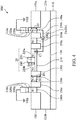
- FIG. 4 shows a cross-sectional view of a semiconductor structure 10D according to an embodiment of the invention.
- the configuration of the semiconductor structure 10B is similar to the semiconductor structure 10C of FIG. 3 , and the difference between the semiconductor structure 10C of FIG. 3 and the semiconductor structure 10D of FIG. 4 is that no interconnect elements (e.g., the contacts 310b and 310c, the vias 320b and 320c and the metals 330b and 330c of FIG. 3 ) are formed on the N-type doped regions 130a and 130b in the semiconductor structure 10D.
- no interconnect elements e.g., the contacts 310b and 310c, the vias 320b and 320c and the metals 330b and 330c of FIG. 3
- FIG. 5 shows a cross-sectional view of a semiconductor structure 10E according to an embodiment of the invention.
- the configuration of the semiconductor structure 10B is similar to the semiconductor structure 10C of FIG. 3 , and the difference between the semiconductor structure 10C of FIG. 3 and the semiconductor structure 10E of FIG. 5 is that no pick-up regions for the N-type well region 120 is present in FIG. 5 .
- no STI regions 150c and 150d and no N-type doped regions 130a and 130b are formed over the N-type well region 120.
- the area of the N-type well region 120 is decreased in the semiconductor structure 10E, and the area of the FDSOI transistor 20 is also decreased.
- the N-type doped region 220a i.e., the drain region of the FDSOI transistor 20
- the N-type doped region 220b i.e., the source region of the FDSOI transistor 20
- the P-type doped region 140b is separated from the P-type doped region 140b by a STI region 150e.
- the undoped layer 125a/125b is formed over the semiconductor substrate 110, and the N-type well region 120 is formed over the semiconductor substrate 110 and between the first region of the undoped layer 125a and the second region of the undoped layer 125b.
- the N-type well region 120 is surrounded by the undoped layer 125a/125b.
- the N-type well region 120 is contact with the undoped layer 125a/125b.
- the undoped layer 125a/125b is used to provide high isolation (or high impedance) for the parasitic capacitor C1.
- the undoped layer 125a/125b is not doped with impurities.
- An equivalent capacitor of the first region of the undoped layer 125a is coupled to the parasitic capacitor C1.
- the drain-bulk capacitor Cdb of the FDSOI transistor 20 has less capacitance than the parasitic capacitor C1. Therefore, the FDSOI transistor 20 of the semiconductor structure 10C has less FOM and less insertion loss.
- one side of the STI region 150b is in contact with the source region of the FDSOI transistor 20, the buried oxide layer 210 and the N-type well region 120. Furthermore, the opposite side of the STI region 150b is in contact with the P-type doped region 140a and the first region of the undoped layer 125a. Similarly, one side of the STI region 150e is in contact with the source region of the FDSOI transistor 20, the buried oxide layer 210 and the N-type well region 120, and the opposite side of the STI region 150e is in contact with the P-type doped region 140b and the second region of the undoped layer 125b.
- the sources and drains of the FDSOI transistor (e.g., 20 of FIGs. 1-5 ) in a RF switching circuit do not need to be coupled to the ground through a resistor. In other words, no resistor coupled to the ground is present in the RF switching circuit. Thus, area and cost of the RF switching circuit are decreased. Furthermore, insertion loss is decreased for RF signal to be received or to be transmitted.
- the drain-bulk capacitor Cdb of the FDSOI transistor 20 is decreased.
- the capacitance value of the drain capacitors is mainly determined by the drain-bulk capacitor Cdb. Therefore, the FDSOI transistor 20 has less FOM and less insertion loss.
- the pick-up regions of the N-type well region 120 can be removed. Thus, the area of the FDSOI transistor 20 is decreased.
Landscapes
- Metal-Oxide And Bipolar Metal-Oxide Semiconductor Integrated Circuits (AREA)
Abstract
Description
- This Application claims priority of
U.S. Provisional Application No. 62/846,805, filed on May 13, 2019 - The invention relates to a semiconductor structure, and more particularly to a semiconductor structure including a fully depleted silicon-on-insulator (FDSOI) transistor.
- Over the past few decades, the size of transistors has been continuously scaled down in order to increase performance and reduce power consumption, leading to better electronic devices that are able to do more useful, important, and valuable things faster, more clearly, and more efficiently.
- Semiconductor-on-insulator (SOI) technology is an attractive candidate to push forward the frontiers imposed by Moore's law. Fully depleted SOI (FDSOI) techniques in particular may provide promising technologies that allow the fabrication of semiconductor devices at technology nodes of 28 nm and beyond. Aside from FDSOI techniques allowing the combination of high performance and low power consumption, complemented by an excellent responsiveness to power management design techniques, the fabrication processes employed in FDSOI techniques are comparatively simple and actually represent a low-risk evolution of conventional planar bulk CMOS techniques.
- Semiconductor structures are provided for a fully depleted silicon-on-insulator (FDSOI) transistor. An embodiment of a semiconductor structure is provided. The semiconductor structure includes a semiconductor substrate, an N-type well region over the semiconductor substrate, a FDSOI transistor formed over the N-type well region, a first shallow trench isolation (STI) region over the N-type well region, a first N-type doped region over the N-type well region, a second STI region over the semiconductor substrate, a first P-type doped region over the semiconductor substrate, and a first interconnection element over the first P-type doped region. The FDSOI transistor includes a buried oxide layer over the N-type well region, a source region over the buried oxide layer, a drain region over the buried oxide layer, a silicon-on-insulator (SOI) layer over the buried oxide layer and between the source and drain regions, and a metal gate over the SOI. The first N-type doped region is separated from the drain region of the FDSOI transistor by the first STI region. The first P-type doped region is separated from the first N-type doped region by the second STI region. The first interconnection element is configured to connect the first P-type doped region to a ground. No interconnection element is formed over the first N-type doped region so that the first N-type doped region and the N-type well region are floating.
- Furthermore, an embodiment of a semiconductor structure is provided. The semiconductor structure includes a semiconductor substrate, an N-type well region over the semiconductor substrate, an undoped layer over the semiconductor substrate and in contact with the N-type well region, a fully depleted silicon-on-insulator (FDSOI) transistor formed over the N-type well region, a first shallow trench isolation (STI) region over the undoped layer, a first P-type doped region over the undoped layer, and a first interconnection element over the first P-type doped region. The FDSOI transistor includes a buried oxide layer over the N-type well region, a source region over the buried oxide layer, a drain region over the buried oxide layer, a silicon-on-insulator (SOI) layer over the buried oxide layer and between the source and drain regions, and a metal gate over the SOI. The first P-type doped region is separated from the drain region of the FDSOI transistor by the first STI region. The first interconnection element is configured to connect the first P-type doped region to a ground.
- Moreover, an embodiment of a semiconductor structure is provided. The semiconductor structure includes a semiconductor substrate, an undoped layer over the semiconductor substrate, a N-type well region over the semiconductor substrate and between a first region and a second region of the undoped layer, a fully depleted silicon-on-insulator (FDSOI) transistor formed over the N-type well region, a first shallow trench isolation (STI) region over the first region of the undoped layer, a first P-type doped region over the first region of the undoped layer, a second STI region over the second region of the undoped layer, and a second P-type doped region over the second region of the undoped layer. The FDSOI transistor includes a buried oxide layer over the N-type well region, a source region over the buried oxide layer, a drain region over the buried oxide layer, a silicon-on-insulator (SOI) layer over the buried oxide layer and between the source and drain regions, and a metal gate over the SOI. The first P-type doped region is separated from the drain region of the FDSOI transistor by the first STI region. The second P-type doped region is separated from the source region of the FDSOI transistor by the second STI region.
- A detailed description is given in the following embodiments with reference to the accompanying drawings. The embodiments described above and described herein below may be combined.
- The invention can be more fully understood by reading the subsequent detailed description and examples with references made to the accompanying drawings, wherein:
-
FIG. 1 shows a cross-sectional view of a semiconductor structure according to an embodiment of the invention. -
FIG. 2 shows a cross-sectional view of a semiconductor structure according to an embodiment of the invention. -
FIG. 3 shows a cross-sectional view of a semiconductor structure according to an embodiment of the invention. -
FIG. 4 shows a cross-sectional view of a semiconductor structure according to an embodiment of the invention. -
FIG. 5 shows a cross-sectional view of a semiconductor structure according to an embodiment of the invention. - The following description is of the best-contemplated mode of carrying out the invention. This description is made for the purpose of illustrating the general principles of the invention and should not be taken in a limiting sense. The scope of the invention is best determined by reference to the appended claims.
- Some variations of the embodiments are described. Throughout the various views and illustrative embodiments, like reference numbers are used to designate like elements. It should be understood that additional operations can be provided before, during, and/or after a disclosed method, and some of the operations described can be replaced or eliminated for other embodiments of the method.
- Furthermore, spatially relative terms, such as "beneath," "below," "lower," "above," "upper" and the like, may be used herein for ease of description to describe one element or feature's relationship to another element(s) or feature(s) as illustrated in the figures.
-
FIG. 1 shows a cross-sectional view of asemiconductor structure 10A according to an embodiment of the invention. An N-type well region 120 is formed on asemiconductor substrate 110. Thesemiconductor substrate 110 may be made of silicon or other semiconductor materials, and thesemiconductor substrate 110 is a P-type substrate. A fully depleted silicon-on-insulator (FDSOI)transistor 20 is formed over the N-type well region 120. A buried oxide (BOX)layer 210 is formed over the N-type well region 120. In some embodiments, theBOX layer 210 may be formed of SiO2, SiN, or combination. The N-type dopedregions BOX layer 210. A silicon-on-insulator (SOI)layer 230 is formed over theBOX layer 210 and between the N-type dopedregions metal gate 240 is formed over theSOI layer 230. The N-type dopedregions FDSOI transistor 20, respectively. Furthermore, a channel of theFDSOI transistor 20 is formed between the N-type dopedregions metal gate 240. In order to simplify the description, other features of theFDSOI transistor 20, such as gate dielectric layer and so on, are omitted. In some embodiments, a heavy doping N-type well region is formed between the N-type well region 120 and thesemiconductor substrate 110. - In
FIG. 1 , the N-type dopedregions type well region 120. The N-type dopedregion 130a is separated from the N-type dopedregion 220a (i.e., the drain region of the FDSOI transistor 20) by a shallow trench isolation (STI)region 150c, and the N-type dopedregion 130b is separated from the N-type dopedregion 220b (i.e., the source region of the FDSOI transistor 20) by aSTI region 150d. TheSTI regions type well region 120. The N-type dopedregions type well region 120. The depth D1 of theSTI regions regions regions regions - The
STI regions region 140a are formed over thesemiconductor substrate 110. In some embodiments, a P-type well region (not shown) is formed over thesemiconductor substrate 110, and theSTI regions region 140a are formed over the P-type well region on the right side of the N-type well region 120. TheSTI region 150b is in contact with the N-type well region 120 and the N-type dopedregion 130a. The P-type dopedregion 140a is separated from the N-type dopedregion 130a by theSTI region 150b, and the P-type dopedregion 140a is disposed between theSTI regions region 140a has the same depth as the N-type dopedregion 130a, i.e., the depth D1. Similarly, theSTI regions region 140b are formed over thesemiconductor substrate 110. In some embodiments, a P-type well region (not shown) is formed over thesemiconductor substrate 110, and theSTI regions region 140b are formed over the P-type well region on the left side of the N-type well region 120. TheSTI region 150e is in contact with the N-type well region 120 and the N-type dopedregion 130b. The P-type dopedregion 140b is separated from the N-type dopedregion 130b by theSTI region 150e, and the P-type dopedregion 140b is disposed between theSTI regions region 140b has the same depth as the N-type dopedregion 130b, i.e., the depth D1. The P-type dopedregions semiconductor substrate 110. - In
FIG. 1 , a plurality of interconnect layers are formed over the N-type dopedregions regions contacts 310a through 310d are the interconnect elements of a first interconnect layer. For example, thecontact 310a is formed on the P-type dopedregion 140a, thecontact 310b is formed on the N-type dopedregion 130a, thecontact 310c is formed on the N-type dopedregion 130b, and thecontact 310d is formed on the P-type dopedregion 140b. - The
vias 320a through 320d are the interconnect elements of a second interconnect layer over the first interconnect layer. For example, the via 320a is formed on thecontact 310a, the via 320b is formed on thecontact 310b, the via 320c is formed on thecontact 310c, and the via 320d is formed on thecontact 310d. Furthermore, themetals 330a through 330d are the interconnect elements of a third interconnect layer over the second interconnect layer. For example, themetal 330a is formed on the via 320a, themetal 330b is formed on the via 320b, themetal 330c is formed on the via 320c, andmetal 330d is formed on the via 320d. - In the
semiconductor structure 10A, a parasitic capacitor C1 is formed by the N-type dopedregion 220a, theBOX layer 210 and the N-type well region 120. In some embodiments, the parasitic capacitor C1 is adjacent to theSTI region 150c. Furthermore, thesemiconductor substrate 110 and the N-type well region 120 form a PN junction to operate as a parasitic diode DD. Therefore, a parasitic path PATH1 including the parasitic capacitor C1 and the parasitic diode DD is formed between the N-type well region 220a and the P-type well region 140a. In some embodiments, the parasitic diode DD is adjacent to theSTI region 150b. Similarly, a parasitic capacitor (not shown) is formed by the N-type dopedregion 220b, theBOX layer 210 and the N-type well region 120. Furthermore, thesemiconductor substrate 110 and the N-type well region 120 form a PN junction to operate as a parasitic diode (not shown) that is adjacent to theSTI region 150e, thus another parasitic path (not shown) is formed between the N-type well region 220b and the P-type well region 310d. In order to simplify the description, only the path PATH1 is illustrated below. - In some embodiments, figure of merit (FOM) is an insertion loss for the
FDSOI transistor 20 used as a switch. Furthermore, the FOM of theFDSOI transistor 20 is mainly obtained according to the following equation:
FDSOI transistor 20, and Coff represent the parasitic capacitor of theFDSOI transistor 20. In some embodiments, the parasitic capacitor of theFDSOI transistor 20 is dominated from the drain capacitors of theFDSOI transistor 20. For theFDSOI transistor 20, the drain capacitors are parasitic capacitors. In some embodiments, the drain capacitors include a drain-gate capacitor Cdg, a drain-source capacitor Cds, and a drain-bulk capacitor Cdb. The capacitance value of the drain capacitors is mainly determined by the drain-bulk capacitor Cdb. - In
FIG. 1 , the anode of the parasitic diode DD is coupled to a ground VSS through the P-type dopedregion 140a, thecontact 310a, the via 320a and themetal 330b. Thus, the parasitic diode DD will not be forward biased. Similarly, the P-type dopedregion 140b, thecontact 310d, the via 320d and themetal 330d are coupled to the ground VSS. Furthermore, the N-type dopedregion 130a is floating, i.e., no signal or power line is connected to themetal 330b, the via 320b and thecontact 310b. Similarly, the N-type dopedregion 130b is floating, i.e., no signal or power line is connected to themetal 330c, the via 320c and thecontact 310c. - In the
semiconductor structure 10A, because no signal is applied to the N-type well region 120 through the N-type dopedregions type well region 120 is floating. Thus, N-type dopedregion 130a is high impedance for the parasitic capacitor C1, and the parasitic capacitor C1 is coupled to the ground VSS through the parasitic diode DD, the P-type dopedregion 140a, thecontact 310a, the via 320a and themetal 330a. In other words, the capacitor C1 and an equivalent capacitor of the parasitic diode DD are coupled in serial between the drain region of theFDSOI transistor 20 and the ground VSS. In general, capacitors coupled in series will reduce the capacitance of the capacitors coupled in series. Thus, the drain-bulk capacitor Cdb of theFDSOI transistor 20 is obtained by connecting the parasitic capacitor C1 and the equivalent capacitor of the parasitic diode DD in series, and the drain-bulk capacitor Cdb of theFDSOI transistor 20 has less capacitance than the parasitic capacitor C1. Therefore, theFDSOI transistor 20 of thesemiconductor structure 10A has less FOM and less insertion loss. -
FIG. 2 shows a cross-sectional view of asemiconductor structure 10B according to an embodiment of the invention. The configuration of thesemiconductor structure 10B is similar to thesemiconductor structure 10A ofFIG. 1 , and the difference between thesemiconductor structure 10A ofFIG. 1 and thesemiconductor structure 10B ofFIG. 2 is that no interconnect elements (e.g., thecontacts vias metals FIG. 1 ) are formed on the N-type dopedregions semiconductor structure 10B. -
FIG. 3 shows a cross-sectional view of asemiconductor structure 10C according to an embodiment of the invention. The configuration of thesemiconductor structure 10C is similar to thesemiconductor structure 10A ofFIG. 1 , and the difference between thesemiconductor structure 10A ofFIG. 1 and thesemiconductor structure 10C ofFIG. 3 is that anundoped layer 125a/125b is formed over thesemiconductor substrate 120 inFIG. 3 . Furthermore, theSTI regions region 140a are formed over a first region of theundoped layer 125a, and theSTI regions region 140b are formed over the a second region ofundoped layer 125b. Theundoped layer 125a/125b is used to provide high isolation (or high impedance) for the parasitic capacitor C1. In some embodiments, theundoped layer 125a /125b is not doped with impurities. An equivalent capacitor of the first region theundoped layer 125a is coupled to the parasitic capacitor C1. Thus, the drain-bulk capacitor Cdb of theFDSOI transistor 20 has less capacitance than the parasitic capacitor C1. Therefore, theFDSOI transistor 20 of thesemiconductor structure 10C has less FOM and less insertion loss. - In some embodiments, the
undoped layer 125a/125b is a light doping P-type well region. Thus, the first region of theundoped layer 125a and the N-type well region 120 form a PN junction to operate as a parasitic diode DD. As described above, the capacitor C1 and an equivalent capacitor of the parasitic diode DD are coupled in serial between the drain region of theFDSOI transistor 20 and the ground VSS. In general, capacitors coupled in series will reduce the capacitance of the capacitors coupled in series. Thus, the drain-bulk capacitor Cdb of theFDSOI transistor 20 is obtained by connecting the parasitic capacitor C1 and an equivalent capacitor of the parasitic diode DD in series, and the drain-bulk capacitor Cdb of theFDSOI transistor 20 has less capacitance than the parasitic capacitor C1. Therefore, theFDSOI transistor 20 of thesemiconductor structure 10C has less FOM and less insertion loss. -
FIG. 4 shows a cross-sectional view of asemiconductor structure 10D according to an embodiment of the invention. The configuration of thesemiconductor structure 10B is similar to thesemiconductor structure 10C ofFIG. 3 , and the difference between thesemiconductor structure 10C ofFIG. 3 and thesemiconductor structure 10D ofFIG. 4 is that no interconnect elements (e.g., thecontacts vias metals FIG. 3 ) are formed on the N-type dopedregions semiconductor structure 10D. -
FIG. 5 shows a cross-sectional view of asemiconductor structure 10E according to an embodiment of the invention. The configuration of thesemiconductor structure 10B is similar to thesemiconductor structure 10C ofFIG. 3 , and the difference between thesemiconductor structure 10C ofFIG. 3 and thesemiconductor structure 10E ofFIG. 5 is that no pick-up regions for the N-type well region 120 is present inFIG. 5 . Compared with thesemiconductor structure 10C ofFIG. 3 , noSTI regions regions type well region 120. Thus, the area of the N-type well region 120 is decreased in thesemiconductor structure 10E, and the area of theFDSOI transistor 20 is also decreased. In thesemiconductor structure 10E, the N-type dopedregion 220a (i.e., the drain region of the FDSOI transistor 20) is separated from the P-type dopedregion 140a by aSTI region 150b, and the N-type dopedregion 220b (i.e., the source region of the FDSOI transistor 20) is separated from the P-type dopedregion 140b by aSTI region 150e. - The
undoped layer 125a/125b is formed over thesemiconductor substrate 110, and the N-type well region 120 is formed over thesemiconductor substrate 110 and between the first region of theundoped layer 125a and the second region of theundoped layer 125b. In some embodiments, the N-type well region 120 is surrounded by theundoped layer 125a/125b. Furthermore, the N-type well region 120 is contact with theundoped layer 125a/125b. As described above, theundoped layer 125a/125b is used to provide high isolation (or high impedance) for the parasitic capacitor C1. In some embodiments, theundoped layer 125a/125b is not doped with impurities. An equivalent capacitor of the first region of theundoped layer 125a is coupled to the parasitic capacitor C1. Thus, the drain-bulk capacitor Cdb of theFDSOI transistor 20 has less capacitance than the parasitic capacitor C1. Therefore, theFDSOI transistor 20 of thesemiconductor structure 10C has less FOM and less insertion loss. - In
FIG. 5 , one side of theSTI region 150b is in contact with the source region of theFDSOI transistor 20, the buriedoxide layer 210 and the N-type well region 120. Furthermore, the opposite side of theSTI region 150b is in contact with the P-type dopedregion 140a and the first region of theundoped layer 125a. Similarly, one side of theSTI region 150e is in contact with the source region of theFDSOI transistor 20, the buriedoxide layer 210 and the N-type well region 120, and the opposite side of theSTI region 150e is in contact with the P-type dopedregion 140b and the second region of theundoped layer 125b. - Compared with the traditional transistors in the traditional RF switching circuit, the sources and drains of the FDSOI transistor (e.g., 20 of
FIGs. 1-5 ) in a RF switching circuit do not need to be coupled to the ground through a resistor. In other words, no resistor coupled to the ground is present in the RF switching circuit. Thus, area and cost of the RF switching circuit are decreased. Furthermore, insertion loss is decreased for RF signal to be received or to be transmitted. - According to the embodiments, by floating the N-
type well region 120 under theFDSOI transistors 20, the drain-bulk capacitor Cdb of theFDSOI transistor 20 is decreased. For theFDSOI transistor 20, the capacitance value of the drain capacitors is mainly determined by the drain-bulk capacitor Cdb. Therefore, theFDSOI transistor 20 has less FOM and less insertion loss. Furthermore, by using theundoped layer 125a/125b, the pick-up regions of the N-type well region 120 can be removed. Thus, the area of theFDSOI transistor 20 is decreased. - While the invention has been described by way of example and in terms of the preferred embodiments, it should be understood that the invention is not limited to the disclosed embodiments. On the contrary, it is intended to cover various modifications and similar arrangements (as would be apparent to those skilled in the art). Therefore, the scope of the appended claims should be accorded the broadest interpretation so as to encompass all such modifications and similar arrangements.
Claims (15)
- A semiconductor structure, comprising:a semiconductor substrate;an N-type well region over the semiconductor substrate;a fully depleted silicon-on-insulator (FDSOI) transistor formed over the N-type well region, comprising:a buried oxide layer over the N-type well region;a source region over the buried oxide layer;a drain region over the buried oxide layer;a silicon-on-insulator (SOI) layer over the buried oxide layer and between the source and drain regions; anda metal gate over the SOI;a first shallow trench isolation (STI) region over the N-type well region;a first N-type doped region over the N-type well region, wherein the first N-type doped region is separated from the drain region of the FDSOI transistor by the first STI region;a second STI region over the semiconductor substrate;a first P-type doped region over the semiconductor substrate, wherein the first P-type doped region is separated from the first N-type doped region by the second STI region; anda first interconnection element over the first P-type doped region and configured to connect the first P-type doped region to a ground.
- The semiconductor structure of claim 1, wherein no interconnection element is formed over the first N-type doped region so that the first N-type doped region and the N-type well region are floating.
- The semiconductor structure as claimed in claim 1 or 2, further comprising:an undoped layer over the semiconductor substrate,wherein the second STI region and the first P-type doped region are separated from the semiconductor substrate by the undoped layer.
- The semiconductor structure as claimed in one of the preceding claims, wherein the first N-type doped region has a depth that is greater than that of the source and drain regions; and/or
wherein the depth of the first N-type doped region is equal to that of the first P-type doped region; and/or
wherein the depth of the first N-type doped region is less than that of the first and second STI regions. - The semiconductor structure as claimed in one of the preceding claims, further comprising:a third STI region over the N-type well region;a second N-type doped region over the N-type well region, wherein the second N-type doped region is separated from the source region of the FDSOI transistor by the third STI region;a fourth STI region over the semiconductor substrate;a second P-type doped region over the semiconductor substrate, wherein the second P-type doped region is separated from the second N-type doped region by the fourth STI region; anda second interconnection element over the second P-type doped region and configured to connect the second P-type doped region to the ground.
- The semiconductor structure as claimed in claim 5, wherein no interconnection element is formed over the second N-type doped region so that the second N-type doped region is floating.
- A semiconductor structure, comprising:a semiconductor substrate;an N-type well region over the semiconductor substrate;an undoped layer over the semiconductor substrate and in contact with the N-type well region;a fully depleted silicon-on-insulator (FDSOI) transistor formed over the N-type well region, comprising:a buried oxide layer over the N-type well region;a source region over the buried oxide layer;a drain region over the buried oxide layer;a silicon-on-insulator (SOI) layer over the buried oxide layer and between the source and drain regions; anda metal gate over the SOI layer;a first shallow trench isolation (STI) region over the undoped layer;a first P-type doped region over the undoped layer, wherein the first P-type doped region is separated from the drain region of the FDSOI transistor by the first STI region; anda first interconnection element over the first P-type doped region and configured to connect the first P-type doped region to a ground.
- The semiconductor structure as claimed in claim 7, wherein the first P-type doped region has a depth that is greater than that of the source and drain regions; and/or wherein a depth of the first P-type doped region is less than that of the first STI region.
- The semiconductor structure as claimed in claim 7 or 8, further comprising:a second STI region over the undoped layer;a second P-type doped region over the undoped layer, wherein the second P-type doped region is separated from the source region of the FDSOI transistor by the second STI region; anda second interconnection element over the second P-type doped region and configured to connect the second P-type doped region to the ground,wherein the N-type well region is surrounded by the undoped layer.
- The semiconductor structure as claimed in claim 9, further comprising:a third STI region over the N-type well region; anda first N-type doped region over the N-type well region and between the first and third STI regions,wherein the first N-type doped region is separated from the drain region of the FDSOI transistor by the third STI region,wherein no interconnection element is formed over the first N-type doped region so that the first N-type doped region and the N-type well region are floating.
- The semiconductor structure as claimed in claim 10, further comprising:a fourth STI region over the N-type well region; anda second N-type doped region over the N-type well region and between the second and fourth STI regions,wherein the second N-type doped region is separated from the source region of the FDSOI transistor by the fourth STI region,wherein no interconnection element is formed over the second N-type doped region so that the second N-type doped region is floating.
- The semiconductor structure of one of claims 9 to 11, whereinthe N-type well region is between a first region and a second region of the undoped layer;the first shallow trench isolation (STI) region is over the first region of the undoped layer;the first P-type doped region is over the first region of the undoped layer;the second STI region is over the second region of the undoped layer; andthe second P-type doped region is over the second region of the undoped layer.
- The semiconductor structure as claimed in claim 12, wherein the first region of the undoped layer is separated from the second region of the undoped layer by the N-type well region, and the N-type well region is in contact with the first and second regions of the undoped layer.
- The semiconductor structure as claimed in claim 12 or 13, wherein a depth of the first and second P-type doped regions is greater than that of the source and drain regions; and/or
wherein a depth of the first and second P-type doped regions is less than that of the first and second STI regions; and/or
wherein the first and second P-type doped regions are coupled to a ground. - The semiconductor structure as claimed in one of claims 12 to 14, wherein one side of the first STI region is in contact with the drain region of the FDSOI transistor, the buried oxide layer and the N-type well region, and an opposite side of the first STI region is in contact with the first P-type doped region and the first region of the undoped layer; or wherein one side of the second STI region is in contact with the source region of the FDSOI transistor, the buried oxide layer and the N-type well region, and the opposite side of the second STI region is in contact with the second P-type doped region and the second region of the undoped layer.
Applications Claiming Priority (2)
| Application Number | Priority Date | Filing Date | Title |
|---|---|---|---|
| US201962846805P | 2019-05-13 | 2019-05-13 | |
| US16/829,017 US11160732B2 (en) | 2019-10-07 | 2020-03-25 | Spittoon lid for disposable containers |
Publications (2)
| Publication Number | Publication Date |
|---|---|
| EP3739629A1 true EP3739629A1 (en) | 2020-11-18 |
| EP3739629B1 EP3739629B1 (en) | 2024-11-20 |
Family
ID=70553815
Family Applications (1)
| Application Number | Title | Priority Date | Filing Date |
|---|---|---|---|
| EP20172844.1A Active EP3739629B1 (en) | 2019-05-13 | 2020-05-05 | Semiconductor structure for fully depleted silicon-on-insulator (fdsoi) transistor |
Country Status (1)
| Country | Link |
|---|---|
| EP (1) | EP3739629B1 (en) |
Citations (5)
| Publication number | Priority date | Publication date | Assignee | Title |
|---|---|---|---|---|
| US6562666B1 (en) * | 2000-10-31 | 2003-05-13 | International Business Machines Corporation | Integrated circuits with reduced substrate capacitance |
| WO2012161859A1 (en) * | 2011-05-24 | 2012-11-29 | International Business Machines Corporation | Improved structure for cmos etsoi with multiple threshold voltages and active well bias capability |
| US20130321057A1 (en) * | 2012-05-30 | 2013-12-05 | Commissariat A L'energie Atomique Et Aux Energies Alternatives | Integrated circuit comprising at least one digital output port having an adjustable impedance, and corresponding adjustment method |
| FR3007577A1 (en) * | 2013-06-19 | 2014-12-26 | Commissariat Energie Atomique | TRANSISTORS WITH DIFFERENT LEVELS OF THRESHOLD VOLTAGES AND ABSENCE OF DISTORTIONS BETWEEN NMOS AND PMOS |
| US20180159471A1 (en) * | 2016-12-06 | 2018-06-07 | Globalfoundries Inc. | Digitally controlled varactor structure for high resolution dco |
-
2020
- 2020-05-05 EP EP20172844.1A patent/EP3739629B1/en active Active
Patent Citations (5)
| Publication number | Priority date | Publication date | Assignee | Title |
|---|---|---|---|---|
| US6562666B1 (en) * | 2000-10-31 | 2003-05-13 | International Business Machines Corporation | Integrated circuits with reduced substrate capacitance |
| WO2012161859A1 (en) * | 2011-05-24 | 2012-11-29 | International Business Machines Corporation | Improved structure for cmos etsoi with multiple threshold voltages and active well bias capability |
| US20130321057A1 (en) * | 2012-05-30 | 2013-12-05 | Commissariat A L'energie Atomique Et Aux Energies Alternatives | Integrated circuit comprising at least one digital output port having an adjustable impedance, and corresponding adjustment method |
| FR3007577A1 (en) * | 2013-06-19 | 2014-12-26 | Commissariat Energie Atomique | TRANSISTORS WITH DIFFERENT LEVELS OF THRESHOLD VOLTAGES AND ABSENCE OF DISTORTIONS BETWEEN NMOS AND PMOS |
| US20180159471A1 (en) * | 2016-12-06 | 2018-06-07 | Globalfoundries Inc. | Digitally controlled varactor structure for high resolution dco |
Also Published As
| Publication number | Publication date |
|---|---|
| EP3739629B1 (en) | 2024-11-20 |
Similar Documents
| Publication | Publication Date | Title |
|---|---|---|
| EP2122669B1 (en) | Radio frequency isolation for soi transistors | |
| US6632723B2 (en) | Semiconductor device | |
| EP3008752B1 (en) | Semiconductor structure having column iii-v isolation regions | |
| KR102299662B1 (en) | Semiconductor Device and Method for Fabricating the Same | |
| CN101771037A (en) | Reducing high-frequency signal loss in substrates | |
| US7709313B2 (en) | High performance capacitors in planar back gates CMOS | |
| US20150221560A1 (en) | Semiconductor device and method of manufacturing the same | |
| EP2363886A1 (en) | Data path cell on an SeOI substrate with a buried back control gate beneath the insulating layer | |
| US9698179B2 (en) | Capacitor structure and method of forming a capacitor structure | |
| US10930675B2 (en) | Semiconductor device | |
| CN111244118B (en) | Integrated chip, method for forming the same, and method for reading the same | |
| US9412863B2 (en) | Enhanced breakdown voltages for high voltage MOSFETS | |
| EP3723124B1 (en) | Semiconductor device | |
| US11107918B2 (en) | Semiconductor structure for fully depleted silicon-on-insulator (FDSOI) transistor | |
| EP3739629B1 (en) | Semiconductor structure for fully depleted silicon-on-insulator (fdsoi) transistor | |
| US20210343636A1 (en) | Semiconductor device and layout design thereof | |
| US7989893B2 (en) | SOI body contact using E-DRAM technology | |
| US20170200783A1 (en) | Electrostatic discharge protection device | |
| US9905480B1 (en) | Semiconductor devices and methods for forming the same | |
| US20150102410A1 (en) | Semiconductor device including stress layer adjacent channel and related methods | |
| CN120035186B (en) | NMOS Device Structure and Formation Method | |
| CN109560065A (en) | A kind of semiconductor device structure and forming method with body contact | |
| US20250318276A1 (en) | Universal gate protection diode | |
| US11437512B2 (en) | Buried channel metal-oxide-semiconductor field-effect transistor (MOSFET) and forming method thereof | |
| US20250392311A1 (en) | Voltage level down-shifting circuit structure with input stage pull-down capacitor |
Legal Events
| Date | Code | Title | Description |
|---|---|---|---|
| PUAI | Public reference made under article 153(3) epc to a published international application that has entered the european phase |
Free format text: ORIGINAL CODE: 0009012 |
|
| STAA | Information on the status of an ep patent application or granted ep patent |
Free format text: STATUS: THE APPLICATION HAS BEEN PUBLISHED |
|
| AK | Designated contracting states |
Kind code of ref document: A1 Designated state(s): AL AT BE BG CH CY CZ DE DK EE ES FI FR GB GR HR HU IE IS IT LI LT LU LV MC MK MT NL NO PL PT RO RS SE SI SK SM TR |
|
| AX | Request for extension of the european patent |
Extension state: BA ME |
|
| STAA | Information on the status of an ep patent application or granted ep patent |
Free format text: STATUS: REQUEST FOR EXAMINATION WAS MADE |
|
| 17P | Request for examination filed |
Effective date: 20210504 |
|
| RBV | Designated contracting states (corrected) |
Designated state(s): AL AT BE BG CH CY CZ DE DK EE ES FI FR GB GR HR HU IE IS IT LI LT LU LV MC MK MT NL NO PL PT RO RS SE SI SK SM TR |
|
| STAA | Information on the status of an ep patent application or granted ep patent |
Free format text: STATUS: EXAMINATION IS IN PROGRESS |
|
| 17Q | First examination report despatched |
Effective date: 20230626 |
|
| P01 | Opt-out of the competence of the unified patent court (upc) registered |
Effective date: 20230627 |
|
| GRAP | Despatch of communication of intention to grant a patent |
Free format text: ORIGINAL CODE: EPIDOSNIGR1 |
|
| STAA | Information on the status of an ep patent application or granted ep patent |
Free format text: STATUS: GRANT OF PATENT IS INTENDED |
|
| INTG | Intention to grant announced |
Effective date: 20240617 |
|
| RAP3 | Party data changed (applicant data changed or rights of an application transferred) |
Owner name: MEDIATEK SINGAPORE PTE. LTD. |
|
| RIN1 | Information on inventor provided before grant (corrected) |
Inventor name: HUANG, SHENG-YI Inventor name: ZENG, ZHENG Inventor name: KO, JEN-WEI |
|
| GRAS | Grant fee paid |
Free format text: ORIGINAL CODE: EPIDOSNIGR3 |
|
| GRAA | (expected) grant |
Free format text: ORIGINAL CODE: 0009210 |
|
| STAA | Information on the status of an ep patent application or granted ep patent |
Free format text: STATUS: THE PATENT HAS BEEN GRANTED |
|
| AK | Designated contracting states |
Kind code of ref document: B1 Designated state(s): AL AT BE BG CH CY CZ DE DK EE ES FI FR GB GR HR HU IE IS IT LI LT LU LV MC MK MT NL NO PL PT RO RS SE SI SK SM TR |
|
| REG | Reference to a national code |
Ref country code: GB Ref legal event code: FG4D |
|
| REG | Reference to a national code |
Ref country code: DE Ref legal event code: R079 Ref document number: 602020041542 Country of ref document: DE Free format text: PREVIOUS MAIN CLASS: H01L0027120000 Ipc: H10D0086000000 |
|
| REG | Reference to a national code |
Ref country code: CH Ref legal event code: EP |
|
| REG | Reference to a national code |
Ref country code: DE Ref legal event code: R096 Ref document number: 602020041542 Country of ref document: DE |
|
| REG | Reference to a national code |
Ref country code: IE Ref legal event code: FG4D |
|
| REG | Reference to a national code |
Ref country code: LT Ref legal event code: MG9D |
|
| REG | Reference to a national code |
Ref country code: NL Ref legal event code: MP Effective date: 20241120 |
|
| PG25 | Lapsed in a contracting state [announced via postgrant information from national office to epo] |
Ref country code: HR Free format text: LAPSE BECAUSE OF FAILURE TO SUBMIT A TRANSLATION OF THE DESCRIPTION OR TO PAY THE FEE WITHIN THE PRESCRIBED TIME-LIMIT Effective date: 20241120 Ref country code: IS Free format text: LAPSE BECAUSE OF FAILURE TO SUBMIT A TRANSLATION OF THE DESCRIPTION OR TO PAY THE FEE WITHIN THE PRESCRIBED TIME-LIMIT Effective date: 20250320 Ref country code: PT Free format text: LAPSE BECAUSE OF FAILURE TO SUBMIT A TRANSLATION OF THE DESCRIPTION OR TO PAY THE FEE WITHIN THE PRESCRIBED TIME-LIMIT Effective date: 20250320 |
|
| PG25 | Lapsed in a contracting state [announced via postgrant information from national office to epo] |
Ref country code: FI Free format text: LAPSE BECAUSE OF FAILURE TO SUBMIT A TRANSLATION OF THE DESCRIPTION OR TO PAY THE FEE WITHIN THE PRESCRIBED TIME-LIMIT Effective date: 20241120 Ref country code: NL Free format text: LAPSE BECAUSE OF FAILURE TO SUBMIT A TRANSLATION OF THE DESCRIPTION OR TO PAY THE FEE WITHIN THE PRESCRIBED TIME-LIMIT Effective date: 20241120 |
|
| REG | Reference to a national code |
Ref country code: AT Ref legal event code: MK05 Ref document number: 1744394 Country of ref document: AT Kind code of ref document: T Effective date: 20241120 |
|
| PG25 | Lapsed in a contracting state [announced via postgrant information from national office to epo] |
Ref country code: BG Free format text: LAPSE BECAUSE OF FAILURE TO SUBMIT A TRANSLATION OF THE DESCRIPTION OR TO PAY THE FEE WITHIN THE PRESCRIBED TIME-LIMIT Effective date: 20241120 |
|
| PG25 | Lapsed in a contracting state [announced via postgrant information from national office to epo] |
Ref country code: ES Free format text: LAPSE BECAUSE OF FAILURE TO SUBMIT A TRANSLATION OF THE DESCRIPTION OR TO PAY THE FEE WITHIN THE PRESCRIBED TIME-LIMIT Effective date: 20241120 |
|
| PG25 | Lapsed in a contracting state [announced via postgrant information from national office to epo] |
Ref country code: NO Free format text: LAPSE BECAUSE OF FAILURE TO SUBMIT A TRANSLATION OF THE DESCRIPTION OR TO PAY THE FEE WITHIN THE PRESCRIBED TIME-LIMIT Effective date: 20250220 |
|
| PG25 | Lapsed in a contracting state [announced via postgrant information from national office to epo] |
Ref country code: GR Free format text: LAPSE BECAUSE OF FAILURE TO SUBMIT A TRANSLATION OF THE DESCRIPTION OR TO PAY THE FEE WITHIN THE PRESCRIBED TIME-LIMIT Effective date: 20250221 Ref country code: AT Free format text: LAPSE BECAUSE OF FAILURE TO SUBMIT A TRANSLATION OF THE DESCRIPTION OR TO PAY THE FEE WITHIN THE PRESCRIBED TIME-LIMIT Effective date: 20241120 Ref country code: LV Free format text: LAPSE BECAUSE OF FAILURE TO SUBMIT A TRANSLATION OF THE DESCRIPTION OR TO PAY THE FEE WITHIN THE PRESCRIBED TIME-LIMIT Effective date: 20241120 |
|
| PG25 | Lapsed in a contracting state [announced via postgrant information from national office to epo] |
Ref country code: PL Free format text: LAPSE BECAUSE OF FAILURE TO SUBMIT A TRANSLATION OF THE DESCRIPTION OR TO PAY THE FEE WITHIN THE PRESCRIBED TIME-LIMIT Effective date: 20241120 |
|
| PG25 | Lapsed in a contracting state [announced via postgrant information from national office to epo] |
Ref country code: RS Free format text: LAPSE BECAUSE OF FAILURE TO SUBMIT A TRANSLATION OF THE DESCRIPTION OR TO PAY THE FEE WITHIN THE PRESCRIBED TIME-LIMIT Effective date: 20250220 |
|
| PG25 | Lapsed in a contracting state [announced via postgrant information from national office to epo] |
Ref country code: SM Free format text: LAPSE BECAUSE OF FAILURE TO SUBMIT A TRANSLATION OF THE DESCRIPTION OR TO PAY THE FEE WITHIN THE PRESCRIBED TIME-LIMIT Effective date: 20241120 |
|
| PGFP | Annual fee paid to national office [announced via postgrant information from national office to epo] |
Ref country code: DE Payment date: 20250325 Year of fee payment: 6 |
|
| PG25 | Lapsed in a contracting state [announced via postgrant information from national office to epo] |
Ref country code: DK Free format text: LAPSE BECAUSE OF FAILURE TO SUBMIT A TRANSLATION OF THE DESCRIPTION OR TO PAY THE FEE WITHIN THE PRESCRIBED TIME-LIMIT Effective date: 20241120 |
|
| PG25 | Lapsed in a contracting state [announced via postgrant information from national office to epo] |
Ref country code: EE Free format text: LAPSE BECAUSE OF FAILURE TO SUBMIT A TRANSLATION OF THE DESCRIPTION OR TO PAY THE FEE WITHIN THE PRESCRIBED TIME-LIMIT Effective date: 20241120 |
|
| PG25 | Lapsed in a contracting state [announced via postgrant information from national office to epo] |
Ref country code: RO Free format text: LAPSE BECAUSE OF FAILURE TO SUBMIT A TRANSLATION OF THE DESCRIPTION OR TO PAY THE FEE WITHIN THE PRESCRIBED TIME-LIMIT Effective date: 20241120 |
|
| PG25 | Lapsed in a contracting state [announced via postgrant information from national office to epo] |
Ref country code: SK Free format text: LAPSE BECAUSE OF FAILURE TO SUBMIT A TRANSLATION OF THE DESCRIPTION OR TO PAY THE FEE WITHIN THE PRESCRIBED TIME-LIMIT Effective date: 20241120 |
|
| PG25 | Lapsed in a contracting state [announced via postgrant information from national office to epo] |
Ref country code: CZ Free format text: LAPSE BECAUSE OF FAILURE TO SUBMIT A TRANSLATION OF THE DESCRIPTION OR TO PAY THE FEE WITHIN THE PRESCRIBED TIME-LIMIT Effective date: 20241120 |
|
| PG25 | Lapsed in a contracting state [announced via postgrant information from national office to epo] |
Ref country code: IT Free format text: LAPSE BECAUSE OF FAILURE TO SUBMIT A TRANSLATION OF THE DESCRIPTION OR TO PAY THE FEE WITHIN THE PRESCRIBED TIME-LIMIT Effective date: 20241120 |
|
| REG | Reference to a national code |
Ref country code: DE Ref legal event code: R097 Ref document number: 602020041542 Country of ref document: DE |
|
| PG25 | Lapsed in a contracting state [announced via postgrant information from national office to epo] |
Ref country code: SE Free format text: LAPSE BECAUSE OF FAILURE TO SUBMIT A TRANSLATION OF THE DESCRIPTION OR TO PAY THE FEE WITHIN THE PRESCRIBED TIME-LIMIT Effective date: 20241120 |
|
| PLBE | No opposition filed within time limit |
Free format text: ORIGINAL CODE: 0009261 |
|
| STAA | Information on the status of an ep patent application or granted ep patent |
Free format text: STATUS: NO OPPOSITION FILED WITHIN TIME LIMIT |
|
| 26N | No opposition filed |
Effective date: 20250821 |
|
| REG | Reference to a national code |
Ref country code: CH Ref legal event code: H13 Free format text: ST27 STATUS EVENT CODE: U-0-0-H10-H13 (AS PROVIDED BY THE NATIONAL OFFICE) Effective date: 20251223 |
|
| PG25 | Lapsed in a contracting state [announced via postgrant information from national office to epo] |
Ref country code: LU Free format text: LAPSE BECAUSE OF NON-PAYMENT OF DUE FEES Effective date: 20250505 |
|
| PG25 | Lapsed in a contracting state [announced via postgrant information from national office to epo] |
Ref country code: CH Free format text: LAPSE BECAUSE OF NON-PAYMENT OF DUE FEES Effective date: 20250531 |
|
| REG | Reference to a national code |
Ref country code: BE Ref legal event code: MM Effective date: 20250531 |
|
| PG25 | Lapsed in a contracting state [announced via postgrant information from national office to epo] |
Ref country code: MC Free format text: LAPSE BECAUSE OF FAILURE TO SUBMIT A TRANSLATION OF THE DESCRIPTION OR TO PAY THE FEE WITHIN THE PRESCRIBED TIME-LIMIT Effective date: 20241120 |
|
| PGFP | Annual fee paid to national office [announced via postgrant information from national office to epo] |
Ref country code: GB Payment date: 20260313 Year of fee payment: 7 |
|
| PG25 | Lapsed in a contracting state [announced via postgrant information from national office to epo] |
Ref country code: IE Free format text: LAPSE BECAUSE OF NON-PAYMENT OF DUE FEES Effective date: 20250505 |
|
| PG25 | Lapsed in a contracting state [announced via postgrant information from national office to epo] |
Ref country code: BE Free format text: LAPSE BECAUSE OF NON-PAYMENT OF DUE FEES Effective date: 20250531 |
|
| PGFP | Annual fee paid to national office [announced via postgrant information from national office to epo] |
Ref country code: FR Payment date: 20260309 Year of fee payment: 7 |