EP3737995B1 - Optical signal modulator comprising a feedback-loop - Google Patents
Optical signal modulator comprising a feedback-loop Download PDFInfo
- Publication number
- EP3737995B1 EP3737995B1 EP18833020.3A EP18833020A EP3737995B1 EP 3737995 B1 EP3737995 B1 EP 3737995B1 EP 18833020 A EP18833020 A EP 18833020A EP 3737995 B1 EP3737995 B1 EP 3737995B1
- Authority
- EP
- European Patent Office
- Prior art keywords
- signal
- optical
- modulator
- output port
- electrical
- Prior art date
- Legal status (The legal status is an assumption and is not a legal conclusion. Google has not performed a legal analysis and makes no representation as to the accuracy of the status listed.)
- Active
Links
Images



Classifications
-
- H—ELECTRICITY
- H04—ELECTRIC COMMUNICATION TECHNIQUE
- H04B—TRANSMISSION
- H04B10/00—Transmission systems employing electromagnetic waves other than radio-waves, e.g. infrared, visible or ultraviolet light, or employing corpuscular radiation, e.g. quantum communication
- H04B10/50—Transmitters
- H04B10/516—Details of coding or modulation
- H04B10/548—Phase or frequency modulation
-
- G—PHYSICS
- G02—OPTICS
- G02F—OPTICAL DEVICES OR ARRANGEMENTS FOR THE CONTROL OF LIGHT BY MODIFICATION OF THE OPTICAL PROPERTIES OF THE MEDIA OF THE ELEMENTS INVOLVED THEREIN; NON-LINEAR OPTICS; FREQUENCY-CHANGING OF LIGHT; OPTICAL LOGIC ELEMENTS; OPTICAL ANALOGUE/DIGITAL CONVERTERS
- G02F1/00—Devices or arrangements for the control of the intensity, colour, phase, polarisation or direction of light arriving from an independent light source, e.g. switching, gating or modulating; Non-linear optics
- G02F1/01—Devices or arrangements for the control of the intensity, colour, phase, polarisation or direction of light arriving from an independent light source, e.g. switching, gating or modulating; Non-linear optics for the control of the intensity, phase, polarisation or colour
- G02F1/0121—Operation of devices; Circuit arrangements, not otherwise provided for in this subclass
- G02F1/0123—Circuits for the control or stabilisation of the bias voltage, e.g. automatic bias control [ABC] feedback loops
-
- H—ELECTRICITY
- H04—ELECTRIC COMMUNICATION TECHNIQUE
- H04B—TRANSMISSION
- H04B10/00—Transmission systems employing electromagnetic waves other than radio-waves, e.g. infrared, visible or ultraviolet light, or employing corpuscular radiation, e.g. quantum communication
- H04B10/07—Arrangements for monitoring or testing transmission systems; Arrangements for fault measurement of transmission systems
- H04B10/075—Arrangements for monitoring or testing transmission systems; Arrangements for fault measurement of transmission systems using an in-service signal
- H04B10/079—Arrangements for monitoring or testing transmission systems; Arrangements for fault measurement of transmission systems using an in-service signal using measurements of the data signal
- H04B10/0799—Monitoring line transmitter or line receiver equipment
-
- H—ELECTRICITY
- H04—ELECTRIC COMMUNICATION TECHNIQUE
- H04B—TRANSMISSION
- H04B10/00—Transmission systems employing electromagnetic waves other than radio-waves, e.g. infrared, visible or ultraviolet light, or employing corpuscular radiation, e.g. quantum communication
- H04B10/50—Transmitters
- H04B10/501—Structural aspects
- H04B10/503—Laser transmitters
- H04B10/505—Laser transmitters using external modulation
- H04B10/5057—Laser transmitters using external modulation using a feedback signal generated by analysing the optical output
- H04B10/50575—Laser transmitters using external modulation using a feedback signal generated by analysing the optical output to control the modulator DC bias
-
- G—PHYSICS
- G02—OPTICS
- G02F—OPTICAL DEVICES OR ARRANGEMENTS FOR THE CONTROL OF LIGHT BY MODIFICATION OF THE OPTICAL PROPERTIES OF THE MEDIA OF THE ELEMENTS INVOLVED THEREIN; NON-LINEAR OPTICS; FREQUENCY-CHANGING OF LIGHT; OPTICAL LOGIC ELEMENTS; OPTICAL ANALOGUE/DIGITAL CONVERTERS
- G02F2201/00—Constructional arrangements not provided for in groups G02F1/00 - G02F7/00
- G02F2201/58—Arrangements comprising a monitoring photodetector
Definitions
- the invention relates to optical signal modulators and methods of operating optical signal modulators.
- optical signal modulator is disclosed for instance in Figure 3 of US Patent 8,269,431 B2 .
- This optical signal modulator comprises a Mach-Zehnder interferometer and a modulator bias control which allows adjusting the operating point of the Mach-Zehnder interferometer.
- An objective of the present invention is to provide an optical signal modulator that provides modulated optical signals with enhanced signal quality.
- a further objective of the present invention is to provide a method of operating an optical signal modulator such that modulated output radiation shows enhanced signal quality.
- An embodiment of the present invention relates to an optical signal modulator according to claim 1.
- the signal delay from the second output port of the modulator unit via the photodetector and the combiner to the electrical ingress port of the modulator unit is preferably shorter than 10 ps.
- the modulator unit may comprise an MMI-coupler having a first output port and a second output port, wherein the first output port of the MMI-coupler forms the first optical output port of the modulator unit and wherein the second output port of the MMI-coupler forms the second optical output port of the modulator unit.
- the modulator unit may comprise a Mach-Zehnder-Interferometer and a phase modulator located in at least one interferometer arm of the Mach-Zehnder-Interferometer, wherein said electrical modulation signal is applied to the at least one phase modulator.
- the Mach-Zehnder-Interferometer may comprise a 3dB-MMI-output-coupler having a first output port and a second output port, wherein the first output port of the MMI-coupler forms the first optical output port of the modulator unit and wherein the second output port of the MMI-coupler forms the second optical output port of the modulator unit.
- the combiner may be configured to subtract the correction signal from the external electrical data signal in order to generate the electrical modulation signal.
- the combiner may comprise an inverter and an adder.
- the inverter may be configured to invert the sign of the correction signal and generate an inverted correction signal.
- the adder may be configured to add the external electrical data signal and the inverted correction signal in order to generate the electrical modulation signal.
- the amplifier may be a transimpedance amplifier.
- the signal delay from the output of the combiner unit via the second output port of the modulator unit, the photodetector, the amplifier to the second electrical input port of the combiner unit is preferably shorter than 10 ps.
- At least one optical filter or optical distortion element may be arranged in the optical signal path between the second optical output port of the modulator unit and the photodetector.
- At least one electrical filter or electrical distortion element may be arranged in the electrical path between the photodetector and the electrical ingress port of the modulator unit.
- a further embodiment of the invention relates to a method according to claim 11.
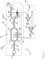
- Figure 1 shows a first exemplary embodiment of an optical signal modulator 300 according to the present invention.
- the optical signal modulator 300 comprises a semiconductor chip 10.
- a first region 20 of the semiconductor chip 10 contains electronic components of the optical signal modulator 300, and a second region 30 of the semiconductor chip 10 contains optical and electro-optical components of the optical signal modulator 300.
- An optical input 41, an optical output 42, an input waveguide 43, an output waveguide 44, a modulator unit 50 and a photodetector 60 are located in the second region 30 of the semiconductor chip 10.
- An amplifier 70 and an electrical signal combiner 80 are located in the first region 20 of the semiconductor chip 10.
- the modulator unit 50 has an optical ingress port 53 for inputting optical radiation P, and an electrical ingress port 54 for inputting an electrical modulation signal Em. As will be explained in further detail below, the modulator unit 50 is configured to modulate the optical radiation P in response to the electrical modulation signal Em. A first portion of the modulated radiation P' leaves the modulator unit 50 at a first optical output port 51. A second portion of the modulated radiation P' leaves at a second optical output port 52.
- the photodetector 60 is connected to the second optical output port 52 and measures the modulated optical radiation P'2 that is emitted at the second optical output port 52.
- the photodetector 60 provides a monitor signal M.
- the amplifier 70 amplifies the monitor signal M and thereby generates a correction signal CS.
- the amplifier 70 may be a transimpedance amplifier.
- the electrical signal combiner 80 has a first input port 81 for inputting an external electrical data signal DS and a second electrical input port 82 for inputting the correction signal CS.
- the combiner 80 may consist of or comprise an operational amplifier as well as other components (e.g. a pre-emphasis unit).
- the electrical signal combiner 80 subtracts the correction signal CS from the external electrical data signal DS and generates the electrical modulation signal Em.
- the electrical modulation signal Em leaves the electrical signal combiner 80 at an electrical output port 83 and reaches the electrical ingress port 54 of the modulator unit 50.
- the signal path that extends from the electrical output port 83 of the electrical combiner 80 - via the electrical ingress port 54 of the modulator unit 50, the Mach-Zehnder-Interferometer 310, the second output port 52 of the modulator unit 50, the photo detector 60, the amplifier 70 - to the second electrical input port 82 of the combiner 80 is hereinafter referred to as feedback path.
- the feedback path is designated by reference sign FBP in Figure 1 .
- modulation path The path that extends from the optical ingress port 53 of the modulator unit 50 to the first optical output port 51 of the modulator unit 50 is hereinafter referred to as modulation path.
- modulation path is designated by reference sign MPH in Figure 1 .
- the signal modulator 300 may be configured to generate an optical data signal of a given bit duration.
- the modulator unit 50, the photodetector 60, the amplifier 70 and the combiner 80 are preferably located in such a close distance relative to another that the feedback path FBP is sufficiently short to provide a signal travel time below 25 % of the bit duration.
- the modulator unit 50, the photodetector 60, the amplifier 70 and the combiner 80 are preferably integrated in the same semiconductor chip 10.
- the signal travel time does not exceed 25 % of the bit duration, higher order nonlinearities that are caused in the modulation path MPH can be significantly compensated such that their impact on the signal quality of the modulated optical signal Pout is relatively small.
- the reduction of the higher order nonlinearities is caused by the feed-back loop (provided by the feedback path FBP) and in particular the combiner 80 which substracts occuring nonlinear distortions from the external data signal DS.
- Figures 2 and 3 visualize the impact of the feedback path FBP on an NRZ-modulated optical signal Pout that exits the modulator unit 50 at the first optical output port 51.
- Figure 2 shows an eye pattern, also known as an eye diagram, without compensation of the higher order nonlinearities, for instance in case that the combiner 80 is switched off.
- Figure 3 shows the respective eye pattern with compensation of the higher order nonlinearities.
- Figure 1 shows the resulting increase of bandwidth due to feedback loop for different feedback gain values gl of the feedback path FBP.
- the bandwidth increases from 5 GHz to 16.3 GHz with increasing gain values gl.
- the bit duration of the external electrical data signal DS is preferably chosen to fulfil the following condition: TB > 4 * Tp wherein TB describes the bit length of the external electrical data signal DS and Tp describes the travel time in the feedback path FBP from the second output 52 to the electrical ingress 54 port of the modulator unit 50.
- the feedback path FBP should preferably be shorter than 5600 um.
- the signal delay caused by the feedback path FBP is shorter than 25 ps (under consideration of the typical signal delay of 7,5 ps caused by the amplifier 70 (if present) and the combiner 80) and the above condition TB > 4*Tp is met.
- the feedback path FBP should preferably be shorter than 800 ⁇ m in order to achieve a signal delay in the feedback path FBP shorter than 10 ps (again under consideration of the typical signal delay of 7,5 ps caused by the amplifier 70 (if present) and the combiner 80).
- the modulator unit 50 may comprise a Mach-Zehnder-Interferometer 310 and a phase modulator 320 located in either one or both of the interferometer arms 311 and 312 of the Mach-Zehnder-Interferometer 311.
- the electrical modulation signal Em is applied to at least one of the interferometer arms 311 and 312.
- the phase modulator 320 may comprise a pn-junction which allows carrier injection or depletion.
- the Mach-Zehnder-Interferometer 310 also comprises an intermediate waveguide 313 and a remote 3dB splitter 314.
- One exit port of the 3dB splitter 314 forms the first optical output port 51 of the modulator unit 50, and the other the second optical output port 52 of the modulator unit 50.
- Figure 5 shows a cross-section of the exemplary embodiment of Figure 1 .
- the input waveguide 43, the output waveguide 44, the modulator unit 50, the photodetector 60, the amplifier 70 and the electrical signal combiner 80 preferably share the same waveguiding silicon layer 13 of the same semiconductor chip 10.
- the semiconductor chip 10 may be based on SOI (silicon on insulator) material, which comprises a silicon substrate 11, a buried oxide layer 12 on top of the substrate 11, and a silicon layer on top of the buried oxide layer. The latter silicon layer preferably forms the waveguiding silicon layer 13.
- the optical input 41 and the optical output 42 may each comprise a deflecting element 41a, 42a and a lens 41a, 41b.
- the deflecting elements 41a and 42a are preferably gratings formed in the waveguiding silicon layer 13 and therefore in the frontend of the semiconductor chip 10.
- the lenses 41b and 42b are preferably formed in at least one backend layer 14 of the backend of the semiconductor chip 10.
- An emitter 200 (e.g. a laser) may be flip-chip mounted on the semiconductor chip 10.
- the emitter 200 may be mounted on the semiconductor chip 10 by means of a submount 210.
- the optical emitter 200 is preferably a continuous wave laser.
- the optical emitter 200 may be a component of the optical signal modulator 300 or an external component.
- the front end and/or backend of the semiconductor chip 10 may further comprise one or more metal layers 15 and vias 16 (via: vertical interconnect access, vertical electrical connection between layers).
- the metal layers 15 and vias 16 can be used to electrically connect components of the semiconductor chip 10 with another and/or with other components of the optical signal modulator 300 (e. g the emitter 200) and/or with external components.
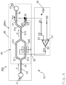
- Figure 6 shows a second exemplary embodiment of an optical signal modulator 300 where in contrast to the optical signal modulator 300 of Figure 1 , the monitor signal M itself forms the correction signal CS and the amplifier 70 is omitted.
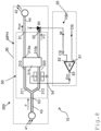
- Figure 7 shows a third exemplary embodiment of an optical signal modulator 300 according to the present invention.
- the Mach-Zehnder-Interferometer 310 comprises a 3dB-MMI-output-coupler 315.
- the 3dB-MMI-output-coupler 315 has a first output port 315a and a second output port 315b.
- the first output port 315a of the MMI-coupler 315 forms the first optical output port 51 of the modulator unit 50 and is connected to the data output port 42 of the optical signal modulator 300.
- the second output port 315b of the MMI-coupler 315 forms the second optical output port 52 of the modulator unit 50 and is connected with the photodetector 60.
- Figure 8 shows a fourth exemplary embodiment of an optical signal modulator 300 where in contrast to the optical signal modulator 300 of Figure 7 , the monitor signal M itself forms the correction signal CS and the amplifier 70 is omitted.
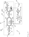
- Figure 9 shows a fifth exemplary embodiment of an optical signal modulator 300 according to the present invention.
- the combiner 80 consists of an inverter 87 and an adder 88.
- the inverter 87 inverts the sign of the correction signal CS and generates an inverted correction signal.
- the adder 88 adds the external electrical data signal DS and the inverted correction signal in order to generate the electrical modulation signal Em.
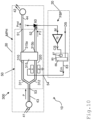
- Figure 10 shows a sixth exemplary embodiment of an optical signal modulator 300 according to the present invention.
- the optical signal modulator 300 comprises a Mach-Zehnder-Interferometer 310 as discussed in connection with Figure 7 .
- the combiner 80 In contrast to the optical signal modulator 300 of Figure 7 , the combiner 80 consists of an inverter 87 and an adder 88.
- the combiner 80 of Figure 10 may be identical with the combiner discussed in connection with Figure 9 .
Landscapes
- Physics & Mathematics (AREA)
- Electromagnetism (AREA)
- Engineering & Computer Science (AREA)
- Computer Networks & Wireless Communication (AREA)
- Signal Processing (AREA)
- Nonlinear Science (AREA)
- Optics & Photonics (AREA)
- General Physics & Mathematics (AREA)
- Optical Modulation, Optical Deflection, Nonlinear Optics, Optical Demodulation, Optical Logic Elements (AREA)
Description
- The invention relates to optical signal modulators and methods of operating optical signal modulators.
- An optical signal modulator is disclosed for instance in
Figure 3 ofUS Patent 8,269,431 B2 . This optical signal modulator comprises a Mach-Zehnder interferometer and a modulator bias control which allows adjusting the operating point of the Mach-Zehnder interferometer. - A signal modulator and a method according to the preambles of
claims US patent publication US 2009/296192 A1 . - An objective of the present invention is to provide an optical signal modulator that provides modulated optical signals with enhanced signal quality.
- A further objective of the present invention is to provide a method of operating an optical signal modulator such that modulated output radiation shows enhanced signal quality.
- An embodiment of the present invention relates to an optical signal modulator according to
claim 1. - The signal delay from the second output port of the modulator unit via the photodetector and the combiner to the electrical ingress port of the modulator unit is preferably shorter than 10 ps.
- The modulator unit may comprise an MMI-coupler having a first output port and a second output port, wherein the first output port of the MMI-coupler forms the first optical output port of the modulator unit and wherein the second output port of the MMI-coupler forms the second optical output port of the modulator unit.
- Alternatively or additionally, the modulator unit may comprise a Mach-Zehnder-Interferometer and a phase modulator located in at least one interferometer arm of the Mach-Zehnder-Interferometer, wherein said electrical modulation signal is applied to the at least one phase modulator.
- The Mach-Zehnder-Interferometer may comprise a 3dB-MMI-output-coupler having a first output port and a second output port, wherein the first output port of the MMI-coupler forms the first optical output port of the modulator unit and wherein the second output port of the MMI-coupler forms the second optical output port of the modulator unit.
- The combiner may be configured to subtract the correction signal from the external electrical data signal in order to generate the electrical modulation signal.
- The combiner may comprise an inverter and an adder. The inverter may be configured to invert the sign of the correction signal and generate an inverted correction signal. The adder may be configured to add the external electrical data signal and the inverted correction signal in order to generate the electrical modulation signal.
- The amplifier may be a transimpedance amplifier.
- The signal delay from the output of the combiner unit via the second output port of the modulator unit, the photodetector, the amplifier to the second electrical input port of the combiner unit is preferably shorter than 10 ps.
- At least one optical filter or optical distortion element may be arranged in the optical signal path between the second optical output port of the modulator unit and the photodetector.
- At least one electrical filter or electrical distortion element may be arranged in the electrical path between the photodetector and the electrical ingress port of the modulator unit.
- A further embodiment of the invention relates to a method according to
claim 11. - In order that the manner in which the above-recited and other advantages of the invention are obtained will be readily understood, a more particular description of the invention briefly described above will be rendered by reference to specific embodiments thereof which are illustrated in the appended drawings. Understanding that these drawings depict only typical embodiments of the invention and are therefore not to be considered to be limiting of its scope, the invention will be described and explained with additional specificity and detail by the use of the accompanying drawings in which
- Fig. 1
- illustrates a first exemplary embodiment of an optical signal modulator according to the present invention in a top view,
- Fig. 2
- illustrates an exemplary eye pattern generated by the embodiment of
Figure 1 without activated feedback loop and without reduction of higher order distortions, - Fig. 3
- illustrates an exemplary eye pattern generated by the embodiment of
Figure 1 with activated feedback loop and with a reduction of higher order distortions, - Fig. 4
- illustrates the resulting bandwidth of the modulated optical output signal for different feedback gain values in the feedback path,
- Fig. 5
- illustrates a cross-section of the exemplary embodiment of
Figure 1 , - Fig. 6 and 8
- illustrate optical signal modulators without amplifier, and
- Fig. 7,9,10
- illustrate further exemplary embodiments of optical signal modulators according to the present invention.
- The preferred embodiments of the present invention will be best understood by reference to the drawings. It will be readily understood that the present invention, as generally described and illustrated in the figures herein, could vary in a wide range. Thus, the following more detailed description of the exemplary embodiments of the present invention, as represented in the figures, is not intended to limit the scope of the invention, as claimed, but is merely representative of presently preferred embodiments of the invention.
-
Figure 1 shows a first exemplary embodiment of anoptical signal modulator 300 according to the present invention. Theoptical signal modulator 300 comprises asemiconductor chip 10. Afirst region 20 of thesemiconductor chip 10 contains electronic components of theoptical signal modulator 300, and asecond region 30 of thesemiconductor chip 10 contains optical and electro-optical components of theoptical signal modulator 300. - An
optical input 41, anoptical output 42, aninput waveguide 43, anoutput waveguide 44, amodulator unit 50 and aphotodetector 60 are located in thesecond region 30 of thesemiconductor chip 10. - An
amplifier 70 and anelectrical signal combiner 80 are located in thefirst region 20 of thesemiconductor chip 10. - The
modulator unit 50 has anoptical ingress port 53 for inputting optical radiation P, and anelectrical ingress port 54 for inputting an electrical modulation signal Em. As will be explained in further detail below, themodulator unit 50 is configured to modulate the optical radiation P in response to the electrical modulation signal Em. A first portion of the modulated radiation P' leaves themodulator unit 50 at a firstoptical output port 51. A second portion of the modulated radiation P' leaves at a secondoptical output port 52. - The
photodetector 60 is connected to the secondoptical output port 52 and measures the modulated optical radiation P'2 that is emitted at the secondoptical output port 52. Thephotodetector 60 provides a monitor signal M. - The
amplifier 70 amplifies the monitor signal M and thereby generates a correction signal CS. Theamplifier 70 may be a transimpedance amplifier. - The electrical signal combiner 80 has a
first input port 81 for inputting an external electrical data signal DS and a secondelectrical input port 82 for inputting the correction signal CS. Thecombiner 80 may consist of or comprise an operational amplifier as well as other components (e.g. a pre-emphasis unit). - The electrical signal combiner 80 subtracts the correction signal CS from the external electrical data signal DS and generates the electrical modulation signal Em. The electrical modulation signal Em leaves the electrical signal combiner 80 at an
electrical output port 83 and reaches theelectrical ingress port 54 of themodulator unit 50. - The signal path that extends from the
electrical output port 83 of the electrical combiner 80 - via theelectrical ingress port 54 of themodulator unit 50, the Mach-Zehnder-Interferometer 310, thesecond output port 52 of themodulator unit 50, thephoto detector 60, the amplifier 70 - to the secondelectrical input port 82 of thecombiner 80 is hereinafter referred to as feedback path. The feedback path is designated by reference sign FBP inFigure 1 . - The path that extends from the
optical ingress port 53 of themodulator unit 50 to the firstoptical output port 51 of themodulator unit 50 is hereinafter referred to as modulation path. The modulation path is designated by reference sign MPH inFigure 1 . - The
signal modulator 300 may be configured to generate an optical data signal of a given bit duration. In this case, themodulator unit 50, thephotodetector 60, theamplifier 70 and thecombiner 80 are preferably located in such a close distance relative to another that the feedback path FBP is sufficiently short to provide a signal travel time below 25 % of the bit duration. To this end, themodulator unit 50, thephotodetector 60, theamplifier 70 and thecombiner 80 are preferably integrated in thesame semiconductor chip 10. - If the signal travel time does not exceed 25 % of the bit duration, higher order nonlinearities that are caused in the modulation path MPH can be significantly compensated such that their impact on the signal quality of the modulated optical signal Pout is relatively small. The reduction of the higher order nonlinearities is caused by the feed-back loop (provided by the feedback path FBP) and in particular the
combiner 80 which substracts occuring nonlinear distortions from the external data signal DS. -
Figures 2 and3 visualize the impact of the feedback path FBP on an NRZ-modulated optical signal Pout that exits themodulator unit 50 at the firstoptical output port 51.Figure 2 shows an eye pattern, also known as an eye diagram, without compensation of the higher order nonlinearities, for instance in case that thecombiner 80 is switched off. -
Figure 3 shows the respective eye pattern with compensation of the higher order nonlinearities. -
Figure 1 shows the resulting increase of bandwidth due to feedback loop for different feedback gain values gl of the feedback path FBP. In the exemplary embodiment ofFigure 4 , the bandwidth increases from 5 GHz to 16.3 GHz with increasing gain values gl. - For a
signal modulator 300 with a given design and therefore a given length of the feedback path FBP, the bit duration of the external electrical data signal DS is preferably chosen to fulfil the following condition:
second output 52 to theelectrical ingress 54 port of themodulator unit 50. - E.g. for optical output signals Pout with a data rate of 10 GBit/s, the feedback path FBP should preferably be shorter than 5600 um. In this case, the signal delay caused by the feedback path FBP is shorter than 25 ps (under consideration of the typical signal delay of 7,5 ps caused by the amplifier 70 (if present) and the combiner 80) and the above condition TB > 4*Tp is met.
- For optical output signals Pout with a data rate of 25 GBit/s, the feedback path FBP should preferably be shorter than 800 µm in order to achieve a signal delay in the feedback path FBP shorter than 10 ps (again under consideration of the typical signal delay of 7,5 ps caused by the amplifier 70 (if present) and the combiner 80).
- The
modulator unit 50 may comprise a Mach-Zehnder-Interferometer 310 and aphase modulator 320 located in either one or both of theinterferometer arms Interferometer 311. The electrical modulation signal Em is applied to at least one of theinterferometer arms phase modulator 320 may comprise a pn-junction which allows carrier injection or depletion. - In the embodiment of
Figure 1 the Mach-Zehnder-Interferometer 310 also comprises anintermediate waveguide 313 and aremote 3dB splitter 314. One exit port of the3dB splitter 314 forms the firstoptical output port 51 of themodulator unit 50, and the other the secondoptical output port 52 of themodulator unit 50. -
Figure 5 shows a cross-section of the exemplary embodiment ofFigure 1 . - The
input waveguide 43, theoutput waveguide 44, themodulator unit 50, thephotodetector 60, theamplifier 70 and theelectrical signal combiner 80 preferably share the samewaveguiding silicon layer 13 of thesame semiconductor chip 10. Thesemiconductor chip 10 may be based on SOI (silicon on insulator) material, which comprises asilicon substrate 11, a buriedoxide layer 12 on top of thesubstrate 11, and a silicon layer on top of the buried oxide layer. The latter silicon layer preferably forms thewaveguiding silicon layer 13. - The
optical input 41 and theoptical output 42 may each comprise a deflectingelement lens elements waveguiding silicon layer 13 and therefore in the frontend of thesemiconductor chip 10. Thelenses backend layer 14 of the backend of thesemiconductor chip 10. - An emitter 200 (e.g. a laser) may be flip-chip mounted on the
semiconductor chip 10. For instance, theemitter 200 may be mounted on thesemiconductor chip 10 by means of asubmount 210. Theoptical emitter 200 is preferably a continuous wave laser. Theoptical emitter 200 may be a component of theoptical signal modulator 300 or an external component. - The front end and/or backend of the
semiconductor chip 10 may further comprise one ormore metal layers 15 and vias 16 (via: vertical interconnect access, vertical electrical connection between layers). The metal layers 15 and vias 16 can be used to electrically connect components of thesemiconductor chip 10 with another and/or with other components of the optical signal modulator 300 (e. g the emitter 200) and/or with external components. -
Figure 6 shows a second exemplary embodiment of anoptical signal modulator 300 where in contrast to theoptical signal modulator 300 ofFigure 1 , the monitor signal M itself forms the correction signal CS and theamplifier 70 is omitted. -
Figure 7 shows a third exemplary embodiment of anoptical signal modulator 300 according to the present invention. In contrast to theoptical signal modulator 300 ofFigure 1 , the Mach-Zehnder-Interferometer 310 comprises a 3dB-MMI-output-coupler 315. The 3dB-MMI-output-coupler 315 has afirst output port 315a and asecond output port 315b. Thefirst output port 315a of the MMI-coupler 315 forms the firstoptical output port 51 of themodulator unit 50 and is connected to thedata output port 42 of theoptical signal modulator 300. Thesecond output port 315b of the MMI-coupler 315 forms the secondoptical output port 52 of themodulator unit 50 and is connected with thephotodetector 60. -
Figure 8 shows a fourth exemplary embodiment of anoptical signal modulator 300 where in contrast to theoptical signal modulator 300 ofFigure 7 , the monitor signal M itself forms the correction signal CS and theamplifier 70 is omitted. -
Figure 9 shows a fifth exemplary embodiment of anoptical signal modulator 300 according to the present invention. In contrast to theoptical signal modulator 300 ofFigure 1 , thecombiner 80 consists of aninverter 87 and anadder 88. Theinverter 87 inverts the sign of the correction signal CS and generates an inverted correction signal. Theadder 88 adds the external electrical data signal DS and the inverted correction signal in order to generate the electrical modulation signal Em. -
Figure 10 shows a sixth exemplary embodiment of anoptical signal modulator 300 according to the present invention. Theoptical signal modulator 300 comprises a Mach-Zehnder-Interferometer 310 as discussed in connection withFigure 7 . - In contrast to the
optical signal modulator 300 ofFigure 7 , thecombiner 80 consists of aninverter 87 and anadder 88. Thecombiner 80 ofFigure 10 may be identical with the combiner discussed in connection withFigure 9 . - The various embodiments and aspects of embodiments of the invention disclosed herein are to be understood not only in the order and context specifically described in this specification, but to include any order and any combination thereof. Whenever the context requires, all words used in the singular number shall be deemed to include the plural and vice versa. Whenever the context requires, all options that are listed with the word "and" shall be deemed to include the world "or" and vice versa, and any combination thereof.
- In the drawings and specification, there have been disclosed a plurality of embodiments of the present invention. The applicant would like to emphasize that each feature of each embodiment may be combined with or added to any other of the embodiments in order to modify the respective embodiment and create additional embodiments. These additional embodiments form a part of the present disclosure and, therefore, the applicant may file further patent claims regarding these additional embodiments at a later stage of the prosecution.
- Further, the applicant would like to emphasize that each feature of each of the following dependent claims may be combined with any of the present independent claims as well as with any other (one ore more) of the present dependent claims (regardless of the present claim structure).
- Therefore, the applicant may direct further patent claims towards other claim combinations at a later stage of the prosecution.
-
- 10
- semiconductor chip
- 11
- silicon substrate
- 12
- buried oxide layer
- 13
- waveguiding silicon layer
- 14
- backend layer
- 15
- metal layer
- 16
- via
- 20
- first region of the semiconductor chip
- 30
- second region of the semiconductor chip
- 41
- optical input
- 41a
- deflecting element
- 41b
- lens
- 42
- optical output
- 42a
- deflecting element
- 42b
- lens
- 43
- input waveguide
- 44
- output waveguide
- 50
- modulator unit
- 51
- first optical output port
- 52
- second optical output port
- 53
- optical ingress port
- 54
- electrical ingress port
- 60
- photodetector
- 70
- amplifier
- 80
- electrical signal combiner
- 81
- first electrical input port
- 82
- second electrical input port
- 83
- electrical output port
- 87
- inverter
- 88
- adder
- 200
- emitter
- 210
- submount
- 300
- optical signal modulator
- 310
- Mach-Zehnder-Interferometer
- 311
- interferometer arm
- 312
- interferometer arm
- 313
- intermediate waveguide
- 314
- 3dB splitter
- 315
- 3dB-MMI-output-coupler
- 315a
- first output port
- 315b
- second output port
- 320
- phase modulator
- CS
- correction signal
- DS
- external electrical data signal
- Em
- electrical modulation signal
- FBP
- feedback path
- gl
- feedback gain value
- M
- monitor signal
- MPH
- modulation path
- P
- optical radiation
- P'
- first portion of the modulated radiation
- P'2
- second portion of the modulated optical radiation
Claims (11)
- Optical signal modulator (300) comprisinga modulator unit (50) having an optical ingress port (53) for inputting optical radiation, a first and second optical output port (51, 52) each for outputting modulated optical radiation, and an electrical ingress port (54) for inputting an electrical modulation signal, the modulator unit (50) being configured to modulate the optical radiation in response to the electrical modulation signal (Em),a photodetector (60) connected to the second optical output port (52) and configured to measure the modulated optical radiation that is emitted at the second optical output port (52), and to provide a monitor signal (M), andan electrical signal combiner (80) having a first input port (81) for inputting an external electrical data signal (DS), a second electrical input port (82) for inputting a correction signal (CS) that is based on the monitor signal (M), and an electrical output port (83) that is connected to the electrical ingress port (54) of the modulator unit (50),wherein the combiner (80) is configured to generate said electrical modulation signal (Em) by combining the external electrical data signal (DS) and the correction signal (CS),characterized in thatan amplifier (70) is electrically arranged between the photodetector (60) and the signal combiner (80) andthe amplifier (70) is configured to amplify the monitor signal (M) and thereby generate the correction signal (CS),wherein the signal modulator (300) is configured to generate an optical data signal of a given bit duration, andwherein the modulator unit (50), the photodetector (60), the amplifier (70) and the combiner (80) are integrated in a same semiconductor chip (10) in such a close distance that the signal path extending from the output port (83) of the combiner (80) via the electrical ingress port (54) of the modulator unit (50), the second output port (52) of the modulator unit (50), the photodetector (60), and the amplifier (70) to the second electrical input port (82) of the combiner (80) is so short that the signal travel time is smaller than 25 % of said given bit duration.
- Optical signal modulator (300) according to claim 1 wherein
the signal delay from the output port (83) of the combiner (80) via the electrical ingress port (54) of the modulator unit (50), the second output port (52) of the modulator unit (50), and the photodetector (60) to the second electrical input port (82) of the combiner (80) is shorter than 25 ps. - Optical signal modulator (300) according to claim 1 wherein
the modulator unit (50), the photodetector (60) and the combiner (80) are integrated in semiconductor layers located on the same semiconductor substrate of the same semiconductor chip (10). - Optical signal modulator (300) according to claim 1 whereinthe modulator unit (50) comprises an MMI-coupler (315) having a first output port (315a) and a second output port (315b),wherein the first output port (315a) of the MMI-coupler (315) forms the first optical output port (51) of the modulator unit (50) as well as a data output port of the optical signal modulator (300), andwherein the second output port (315b) of the MMI-coupler (315) forms the second optical output port (52) of the modulator unit (50).
- Optical signal modulator (300) according to claim 1wherein the modulator unit (50) comprises a Mach-Zehnder-Interferometer (310) and a phase modulator (300) located in at least one interferometer arm (311, 312) of the Mach-Zehnder-Interferometer (310), andwherein said electrical modulation signal (Em) is applied to the at least one phase modulator (320).
- Optical signal modulator (300) according to claim 5wherein the Mach-Zehnder-Interferometer (310) comprises a 3dB-output-coupler (315),wherein the 3dB-output-coupler (315)is an MMI-coupler having a first output port (315a) and a second output port (315b),wherein the first output port (315a) of the MMI-coupler (315) forms the first optical output port (51) of the modulator unit (50), andthe second output port (315b) of the MMI-coupler (315) forms the second optical output port (52) of the modulator unit (50).
- Optical signal modulator (300) according to claim 1 wherein
the combiner (80) is configured to subtract the correction signal (CS) from the external electrical data signal (DS) in order to generate the electrical modulation signal (Em). - Optical signal modulator (300) according to claim 1 whereinthe combiner (80) comprises an inverter (87) and an adder (88),wherein the inverter (87) is configured to invert the sign of the correction signal (CS) and generate an inverted correction signal, andwherein the adder (88) is configured to add the external electrical data signal and the inverted correction signal in order to generate the electrical modulation signal (Em) .
- Optical signal modulator (300) according to claim 1 wherein
the amplifier (70) is a transimpedance amplifier. - Optical signal modulator (300) according to claim 1 wherein
at least one optical filter or optical distortion element is arranged in the optical signal path between the second optical output port (52) of the modulator unit (50) and the photodetector (60) or between the photodetector (60) and the electrical ingress port (54) of the modulator unit (50). - Method for generating an optical data signal based on an external electrical data signal in an optical signal modulator (300) according to any of claims 1-10, comprising the steps ofmodulating optical radiation by applying an electrical modulation signal (Em) to an electrical ingress port (54) of the modulator unit (50), said modulator unit (50) emitting said optical data signal at a first optical output port (51) of the modulator unit (50),measuring the modulated optical radiation that is emitted at a second optical output (52) of the modulator unit (50) and providing a monitor signal (M), andelectrically combining a correction signal (CS) that is based on the monitor signal (M), and said external electrical data signal (DS) and thereby forming said electrical modulation signal (Em);characterized in that
the bit duration of the external electrical data signal (DS) is chosen to fulfil the following condition:
Applications Claiming Priority (2)
| Application Number | Priority Date | Filing Date | Title |
|---|---|---|---|
| US15/870,219 US10476600B2 (en) | 2018-01-12 | 2018-01-12 | Optical signal modulator comprising a feedback-loop |
| PCT/EP2018/085595 WO2019137766A1 (en) | 2018-01-12 | 2018-12-18 | Optical signal modulator comprising a feedback-loop |
Publications (2)
| Publication Number | Publication Date |
|---|---|
| EP3737995A1 EP3737995A1 (en) | 2020-11-18 |
| EP3737995B1 true EP3737995B1 (en) | 2024-03-27 |
Family
ID=65010736
Family Applications (1)
| Application Number | Title | Priority Date | Filing Date |
|---|---|---|---|
| EP18833020.3A Active EP3737995B1 (en) | 2018-01-12 | 2018-12-18 | Optical signal modulator comprising a feedback-loop |
Country Status (4)
| Country | Link |
|---|---|
| US (1) | US10476600B2 (en) |
| EP (1) | EP3737995B1 (en) |
| CN (1) | CN111527443B (en) |
| WO (1) | WO2019137766A1 (en) |
Families Citing this family (2)
| Publication number | Priority date | Publication date | Assignee | Title |
|---|---|---|---|---|
| US12197051B2 (en) * | 2019-05-23 | 2025-01-14 | Nippon Telegraph And Telephone Corporation | Optical inspection circuit and optical inspection method |
| US10761352B1 (en) * | 2019-09-11 | 2020-09-01 | Sicoya Gmbh | Optical device |
Family Cites Families (10)
| Publication number | Priority date | Publication date | Assignee | Title |
|---|---|---|---|---|
| US6469817B1 (en) * | 1999-06-18 | 2002-10-22 | Trw Inc. | Apparatus and method employing two optical signals for stabilizing an optical interferometer |
| US7425696B2 (en) * | 2004-02-19 | 2008-09-16 | National Institute Of Information And Communications Technology Incorporated Administrative Agency | Photoelectric oscillator |
| US7463802B2 (en) | 2006-01-13 | 2008-12-09 | Emcore Corporation | Integrated circuit for adjusting bias in optical transmitter with external modulator |
| JP2009288509A (en) | 2008-05-29 | 2009-12-10 | Fujitsu Ltd | Optical modulation apparatus |
| US7977622B2 (en) | 2009-02-09 | 2011-07-12 | Hewlett-Packard Development Company, L.P. | Tuning an optical resonator using a feedback signal representing an average DC balanced coding |
| US8269431B2 (en) | 2009-06-15 | 2012-09-18 | The Board Of Trustees Of The University Of Illinois | Method and apparatus for producing linearized optical signals |
| US8543010B2 (en) | 2010-02-24 | 2013-09-24 | Jds Uniphase Corporation | Bias control in an optical modulator and transmitter |
| JP5853386B2 (en) | 2010-12-16 | 2016-02-09 | 富士通オプティカルコンポーネンツ株式会社 | Light modulation device and light modulation control method |
| CN102769496A (en) * | 2012-07-28 | 2012-11-07 | 文鸿 | Device and method for generating octuple-frequency optical millimeter waves |
| CN106646932B (en) * | 2016-12-29 | 2023-05-23 | 中国电子科技集团公司第三十四研究所 | A DC Bias Operating Point Control Loop of a Mach-Zehnder Intensity Modulator |
-
2018
- 2018-01-12 US US15/870,219 patent/US10476600B2/en active Active
- 2018-12-18 EP EP18833020.3A patent/EP3737995B1/en active Active
- 2018-12-18 CN CN201880084904.3A patent/CN111527443B/en active Active
- 2018-12-18 WO PCT/EP2018/085595 patent/WO2019137766A1/en not_active Ceased
Also Published As
| Publication number | Publication date |
|---|---|
| WO2019137766A1 (en) | 2019-07-18 |
| US20190222319A1 (en) | 2019-07-18 |
| US10476600B2 (en) | 2019-11-12 |
| CN111527443A (en) | 2020-08-11 |
| CN111527443B (en) | 2023-11-21 |
| EP3737995A1 (en) | 2020-11-18 |
Similar Documents
| Publication | Publication Date | Title |
|---|---|---|
| US8224188B2 (en) | Even-order harmonic cancellation and increased RF gain using dual-output mach-zehnder modulator with two wavelength input | |
| JP6661913B2 (en) | Optical module and optical transmitter using the same | |
| US7302120B2 (en) | Optical modulator | |
| JP4272585B2 (en) | Optical modulation apparatus, optical transmission apparatus, and optical modulation method | |
| US10305599B2 (en) | Optical transmitter module | |
| WO2002082693A1 (en) | Optical linearizer for fiber communications | |
| US10749601B2 (en) | Optical transceiver | |
| CN111326599B (en) | A silicon-based optoelectronic integrated chip device and a launch system with the silicon-based optoelectronic integrated chip device | |
| JP6034811B2 (en) | Wavelength multiplexing transmitter | |
| US20060072924A1 (en) | Duo-binary optical transmitter tolerant to chromatic dispersion | |
| US10476600B2 (en) | Optical signal modulator comprising a feedback-loop | |
| US20050013618A1 (en) | Optical receiving method, optical receiver and optical transmission system using the same | |
| EP1816506A1 (en) | Optical modulator for burst-mode transmission | |
| JP2004312678A (en) | Duobinary optical transmission equipment | |
| JP2003348022A (en) | Optical transmitter | |
| US7746909B2 (en) | Method and systems for optimizing laser and electro-absorption modulator performance for long-haul optical transmission | |
| US20060018667A1 (en) | Optical transmission apparatus using duobinary modulation | |
| JP2019047053A (en) | Multi-wavelength light source | |
| JP2001159750A (en) | Optical transmitter and optical modulator | |
| US7577369B1 (en) | Systems for deploying an optical network | |
| JP6547116B2 (en) | Light modulator | |
| JP4654570B2 (en) | Stimulated Brillouin scattering suppression device and optical fiber transmission system using the same | |
| JPH09246633A (en) | Light source device for optical communication | |
| JP3323065B2 (en) | Optical communication device | |
| US20050141072A1 (en) | Electroabsorption modulator with two sections |
Legal Events
| Date | Code | Title | Description |
|---|---|---|---|
| STAA | Information on the status of an ep patent application or granted ep patent |
Free format text: STATUS: UNKNOWN |
|
| STAA | Information on the status of an ep patent application or granted ep patent |
Free format text: STATUS: THE INTERNATIONAL PUBLICATION HAS BEEN MADE |
|
| PUAI | Public reference made under article 153(3) epc to a published international application that has entered the european phase |
Free format text: ORIGINAL CODE: 0009012 |
|
| STAA | Information on the status of an ep patent application or granted ep patent |
Free format text: STATUS: REQUEST FOR EXAMINATION WAS MADE |
|
| 17P | Request for examination filed |
Effective date: 20200624 |
|
| AK | Designated contracting states |
Kind code of ref document: A1 Designated state(s): AL AT BE BG CH CY CZ DE DK EE ES FI FR GB GR HR HU IE IS IT LI LT LU LV MC MK MT NL NO PL PT RO RS SE SI SK SM TR |
|
| AX | Request for extension of the european patent |
Extension state: BA ME |
|
| DAV | Request for validation of the european patent (deleted) | ||
| DAX | Request for extension of the european patent (deleted) | ||
| STAA | Information on the status of an ep patent application or granted ep patent |
Free format text: STATUS: EXAMINATION IS IN PROGRESS |
|
| 17Q | First examination report despatched |
Effective date: 20220202 |
|
| GRAP | Despatch of communication of intention to grant a patent |
Free format text: ORIGINAL CODE: EPIDOSNIGR1 |
|
| STAA | Information on the status of an ep patent application or granted ep patent |
Free format text: STATUS: GRANT OF PATENT IS INTENDED |
|
| INTG | Intention to grant announced |
Effective date: 20231024 |
|
| GRAS | Grant fee paid |
Free format text: ORIGINAL CODE: EPIDOSNIGR3 |
|
| GRAA | (expected) grant |
Free format text: ORIGINAL CODE: 0009210 |
|
| STAA | Information on the status of an ep patent application or granted ep patent |
Free format text: STATUS: THE PATENT HAS BEEN GRANTED |
|
| AK | Designated contracting states |
Kind code of ref document: B1 Designated state(s): AL AT BE BG CH CY CZ DE DK EE ES FI FR GB GR HR HU IE IS IT LI LT LU LV MC MK MT NL NO PL PT RO RS SE SI SK SM TR |
|
| REG | Reference to a national code |
Ref country code: GB Ref legal event code: FG4D |
|
| REG | Reference to a national code |
Ref country code: CH Ref legal event code: EP |
|
| REG | Reference to a national code |
Ref country code: DE Ref legal event code: R096 Ref document number: 602018067260 Country of ref document: DE |
|
| REG | Reference to a national code |
Ref country code: IE Ref legal event code: FG4D |
|
| PG25 | Lapsed in a contracting state [announced via postgrant information from national office to epo] |
Ref country code: LT Free format text: LAPSE BECAUSE OF FAILURE TO SUBMIT A TRANSLATION OF THE DESCRIPTION OR TO PAY THE FEE WITHIN THE PRESCRIBED TIME-LIMIT Effective date: 20240327 |
|
| REG | Reference to a national code |
Ref country code: LT Ref legal event code: MG9D |
|
| PG25 | Lapsed in a contracting state [announced via postgrant information from national office to epo] |
Ref country code: GR Free format text: LAPSE BECAUSE OF FAILURE TO SUBMIT A TRANSLATION OF THE DESCRIPTION OR TO PAY THE FEE WITHIN THE PRESCRIBED TIME-LIMIT Effective date: 20240628 |
|
| PG25 | Lapsed in a contracting state [announced via postgrant information from national office to epo] |
Ref country code: RS Free format text: LAPSE BECAUSE OF FAILURE TO SUBMIT A TRANSLATION OF THE DESCRIPTION OR TO PAY THE FEE WITHIN THE PRESCRIBED TIME-LIMIT Effective date: 20240627 Ref country code: HR Free format text: LAPSE BECAUSE OF FAILURE TO SUBMIT A TRANSLATION OF THE DESCRIPTION OR TO PAY THE FEE WITHIN THE PRESCRIBED TIME-LIMIT Effective date: 20240327 |
|
| PG25 | Lapsed in a contracting state [announced via postgrant information from national office to epo] |
Ref country code: RS Free format text: LAPSE BECAUSE OF FAILURE TO SUBMIT A TRANSLATION OF THE DESCRIPTION OR TO PAY THE FEE WITHIN THE PRESCRIBED TIME-LIMIT Effective date: 20240627 Ref country code: NO Free format text: LAPSE BECAUSE OF FAILURE TO SUBMIT A TRANSLATION OF THE DESCRIPTION OR TO PAY THE FEE WITHIN THE PRESCRIBED TIME-LIMIT Effective date: 20240627 Ref country code: LT Free format text: LAPSE BECAUSE OF FAILURE TO SUBMIT A TRANSLATION OF THE DESCRIPTION OR TO PAY THE FEE WITHIN THE PRESCRIBED TIME-LIMIT Effective date: 20240327 Ref country code: HR Free format text: LAPSE BECAUSE OF FAILURE TO SUBMIT A TRANSLATION OF THE DESCRIPTION OR TO PAY THE FEE WITHIN THE PRESCRIBED TIME-LIMIT Effective date: 20240327 Ref country code: GR Free format text: LAPSE BECAUSE OF FAILURE TO SUBMIT A TRANSLATION OF THE DESCRIPTION OR TO PAY THE FEE WITHIN THE PRESCRIBED TIME-LIMIT Effective date: 20240628 Ref country code: FI Free format text: LAPSE BECAUSE OF FAILURE TO SUBMIT A TRANSLATION OF THE DESCRIPTION OR TO PAY THE FEE WITHIN THE PRESCRIBED TIME-LIMIT Effective date: 20240327 Ref country code: BG Free format text: LAPSE BECAUSE OF FAILURE TO SUBMIT A TRANSLATION OF THE DESCRIPTION OR TO PAY THE FEE WITHIN THE PRESCRIBED TIME-LIMIT Effective date: 20240327 |
|
| REG | Reference to a national code |
Ref country code: NL Ref legal event code: MP Effective date: 20240327 |
|
| PG25 | Lapsed in a contracting state [announced via postgrant information from national office to epo] |
Ref country code: SE Free format text: LAPSE BECAUSE OF FAILURE TO SUBMIT A TRANSLATION OF THE DESCRIPTION OR TO PAY THE FEE WITHIN THE PRESCRIBED TIME-LIMIT Effective date: 20240327 Ref country code: LV Free format text: LAPSE BECAUSE OF FAILURE TO SUBMIT A TRANSLATION OF THE DESCRIPTION OR TO PAY THE FEE WITHIN THE PRESCRIBED TIME-LIMIT Effective date: 20240327 |
|
| PG25 | Lapsed in a contracting state [announced via postgrant information from national office to epo] |
Ref country code: NL Free format text: LAPSE BECAUSE OF FAILURE TO SUBMIT A TRANSLATION OF THE DESCRIPTION OR TO PAY THE FEE WITHIN THE PRESCRIBED TIME-LIMIT Effective date: 20240327 |
|
| REG | Reference to a national code |
Ref country code: AT Ref legal event code: MK05 Ref document number: 1670475 Country of ref document: AT Kind code of ref document: T Effective date: 20240327 |
|
| PG25 | Lapsed in a contracting state [announced via postgrant information from national office to epo] |
Ref country code: NL Free format text: LAPSE BECAUSE OF FAILURE TO SUBMIT A TRANSLATION OF THE DESCRIPTION OR TO PAY THE FEE WITHIN THE PRESCRIBED TIME-LIMIT Effective date: 20240327 |
|
| PG25 | Lapsed in a contracting state [announced via postgrant information from national office to epo] |
Ref country code: IS Free format text: LAPSE BECAUSE OF FAILURE TO SUBMIT A TRANSLATION OF THE DESCRIPTION OR TO PAY THE FEE WITHIN THE PRESCRIBED TIME-LIMIT Effective date: 20240727 |
|
| PG25 | Lapsed in a contracting state [announced via postgrant information from national office to epo] |
Ref country code: PT Free format text: LAPSE BECAUSE OF FAILURE TO SUBMIT A TRANSLATION OF THE DESCRIPTION OR TO PAY THE FEE WITHIN THE PRESCRIBED TIME-LIMIT Effective date: 20240729 Ref country code: SM Free format text: LAPSE BECAUSE OF FAILURE TO SUBMIT A TRANSLATION OF THE DESCRIPTION OR TO PAY THE FEE WITHIN THE PRESCRIBED TIME-LIMIT Effective date: 20240327 |
|
| PG25 | Lapsed in a contracting state [announced via postgrant information from national office to epo] |
Ref country code: ES Free format text: LAPSE BECAUSE OF FAILURE TO SUBMIT A TRANSLATION OF THE DESCRIPTION OR TO PAY THE FEE WITHIN THE PRESCRIBED TIME-LIMIT Effective date: 20240327 |
|
| PG25 | Lapsed in a contracting state [announced via postgrant information from national office to epo] |
Ref country code: CZ Free format text: LAPSE BECAUSE OF FAILURE TO SUBMIT A TRANSLATION OF THE DESCRIPTION OR TO PAY THE FEE WITHIN THE PRESCRIBED TIME-LIMIT Effective date: 20240327 Ref country code: EE Free format text: LAPSE BECAUSE OF FAILURE TO SUBMIT A TRANSLATION OF THE DESCRIPTION OR TO PAY THE FEE WITHIN THE PRESCRIBED TIME-LIMIT Effective date: 20240327 |
|
| PG25 | Lapsed in a contracting state [announced via postgrant information from national office to epo] |
Ref country code: AT Free format text: LAPSE BECAUSE OF FAILURE TO SUBMIT A TRANSLATION OF THE DESCRIPTION OR TO PAY THE FEE WITHIN THE PRESCRIBED TIME-LIMIT Effective date: 20240327 |
|
| PG25 | Lapsed in a contracting state [announced via postgrant information from national office to epo] |
Ref country code: PL Free format text: LAPSE BECAUSE OF FAILURE TO SUBMIT A TRANSLATION OF THE DESCRIPTION OR TO PAY THE FEE WITHIN THE PRESCRIBED TIME-LIMIT Effective date: 20240327 |
|
| PG25 | Lapsed in a contracting state [announced via postgrant information from national office to epo] |
Ref country code: SK Free format text: LAPSE BECAUSE OF FAILURE TO SUBMIT A TRANSLATION OF THE DESCRIPTION OR TO PAY THE FEE WITHIN THE PRESCRIBED TIME-LIMIT Effective date: 20240327 |
|
| PG25 | Lapsed in a contracting state [announced via postgrant information from national office to epo] |
Ref country code: SM Free format text: LAPSE BECAUSE OF FAILURE TO SUBMIT A TRANSLATION OF THE DESCRIPTION OR TO PAY THE FEE WITHIN THE PRESCRIBED TIME-LIMIT Effective date: 20240327 Ref country code: SK Free format text: LAPSE BECAUSE OF FAILURE TO SUBMIT A TRANSLATION OF THE DESCRIPTION OR TO PAY THE FEE WITHIN THE PRESCRIBED TIME-LIMIT Effective date: 20240327 Ref country code: RO Free format text: LAPSE BECAUSE OF FAILURE TO SUBMIT A TRANSLATION OF THE DESCRIPTION OR TO PAY THE FEE WITHIN THE PRESCRIBED TIME-LIMIT Effective date: 20240327 Ref country code: PT Free format text: LAPSE BECAUSE OF FAILURE TO SUBMIT A TRANSLATION OF THE DESCRIPTION OR TO PAY THE FEE WITHIN THE PRESCRIBED TIME-LIMIT Effective date: 20240729 Ref country code: PL Free format text: LAPSE BECAUSE OF FAILURE TO SUBMIT A TRANSLATION OF THE DESCRIPTION OR TO PAY THE FEE WITHIN THE PRESCRIBED TIME-LIMIT Effective date: 20240327 Ref country code: IS Free format text: LAPSE BECAUSE OF FAILURE TO SUBMIT A TRANSLATION OF THE DESCRIPTION OR TO PAY THE FEE WITHIN THE PRESCRIBED TIME-LIMIT Effective date: 20240727 Ref country code: ES Free format text: LAPSE BECAUSE OF FAILURE TO SUBMIT A TRANSLATION OF THE DESCRIPTION OR TO PAY THE FEE WITHIN THE PRESCRIBED TIME-LIMIT Effective date: 20240327 Ref country code: EE Free format text: LAPSE BECAUSE OF FAILURE TO SUBMIT A TRANSLATION OF THE DESCRIPTION OR TO PAY THE FEE WITHIN THE PRESCRIBED TIME-LIMIT Effective date: 20240327 Ref country code: CZ Free format text: LAPSE BECAUSE OF FAILURE TO SUBMIT A TRANSLATION OF THE DESCRIPTION OR TO PAY THE FEE WITHIN THE PRESCRIBED TIME-LIMIT Effective date: 20240327 Ref country code: AT Free format text: LAPSE BECAUSE OF FAILURE TO SUBMIT A TRANSLATION OF THE DESCRIPTION OR TO PAY THE FEE WITHIN THE PRESCRIBED TIME-LIMIT Effective date: 20240327 |
|
| PG25 | Lapsed in a contracting state [announced via postgrant information from national office to epo] |
Ref country code: IT Free format text: LAPSE BECAUSE OF FAILURE TO SUBMIT A TRANSLATION OF THE DESCRIPTION OR TO PAY THE FEE WITHIN THE PRESCRIBED TIME-LIMIT Effective date: 20240327 |
|
| PG25 | Lapsed in a contracting state [announced via postgrant information from national office to epo] |
Ref country code: IT Free format text: LAPSE BECAUSE OF FAILURE TO SUBMIT A TRANSLATION OF THE DESCRIPTION OR TO PAY THE FEE WITHIN THE PRESCRIBED TIME-LIMIT Effective date: 20240327 |
|
| REG | Reference to a national code |
Ref country code: DE Ref legal event code: R097 Ref document number: 602018067260 Country of ref document: DE |
|
| PG25 | Lapsed in a contracting state [announced via postgrant information from national office to epo] |
Ref country code: DK Free format text: LAPSE BECAUSE OF FAILURE TO SUBMIT A TRANSLATION OF THE DESCRIPTION OR TO PAY THE FEE WITHIN THE PRESCRIBED TIME-LIMIT Effective date: 20240327 |
|
| PG25 | Lapsed in a contracting state [announced via postgrant information from national office to epo] |
Ref country code: DK Free format text: LAPSE BECAUSE OF FAILURE TO SUBMIT A TRANSLATION OF THE DESCRIPTION OR TO PAY THE FEE WITHIN THE PRESCRIBED TIME-LIMIT Effective date: 20240327 |
|
| PLBE | No opposition filed within time limit |
Free format text: ORIGINAL CODE: 0009261 |
|
| STAA | Information on the status of an ep patent application or granted ep patent |
Free format text: STATUS: NO OPPOSITION FILED WITHIN TIME LIMIT |
|
| 26N | No opposition filed |
Effective date: 20250103 |
|
| PG25 | Lapsed in a contracting state [announced via postgrant information from national office to epo] |
Ref country code: SI Free format text: LAPSE BECAUSE OF FAILURE TO SUBMIT A TRANSLATION OF THE DESCRIPTION OR TO PAY THE FEE WITHIN THE PRESCRIBED TIME-LIMIT Effective date: 20240327 |
|
| PG25 | Lapsed in a contracting state [announced via postgrant information from national office to epo] |
Ref country code: MC Free format text: LAPSE BECAUSE OF FAILURE TO SUBMIT A TRANSLATION OF THE DESCRIPTION OR TO PAY THE FEE WITHIN THE PRESCRIBED TIME-LIMIT Effective date: 20240327 |
|
| REG | Reference to a national code |
Ref country code: CH Ref legal event code: PL |
|
| PG25 | Lapsed in a contracting state [announced via postgrant information from national office to epo] |
Ref country code: LU Free format text: LAPSE BECAUSE OF NON-PAYMENT OF DUE FEES Effective date: 20241218 |
|
| REG | Reference to a national code |
Ref country code: BE Ref legal event code: MM Effective date: 20241231 |
|
| PG25 | Lapsed in a contracting state [announced via postgrant information from national office to epo] |
Ref country code: BE Free format text: LAPSE BECAUSE OF NON-PAYMENT OF DUE FEES Effective date: 20241231 |
|
| PG25 | Lapsed in a contracting state [announced via postgrant information from national office to epo] |
Ref country code: CH Free format text: LAPSE BECAUSE OF NON-PAYMENT OF DUE FEES Effective date: 20241231 |
|
| PG25 | Lapsed in a contracting state [announced via postgrant information from national office to epo] |
Ref country code: IE Free format text: LAPSE BECAUSE OF NON-PAYMENT OF DUE FEES Effective date: 20241218 |
|
| PGFP | Annual fee paid to national office [announced via postgrant information from national office to epo] |
Ref country code: GB Payment date: 20251218 Year of fee payment: 8 |
|
| PGFP | Annual fee paid to national office [announced via postgrant information from national office to epo] |
Ref country code: FR Payment date: 20251218 Year of fee payment: 8 |
|
| PGFP | Annual fee paid to national office [announced via postgrant information from national office to epo] |
Ref country code: DE Payment date: 20251231 Year of fee payment: 8 |
|
| PG25 | Lapsed in a contracting state [announced via postgrant information from national office to epo] |
Ref country code: CY Free format text: LAPSE BECAUSE OF FAILURE TO SUBMIT A TRANSLATION OF THE DESCRIPTION OR TO PAY THE FEE WITHIN THE PRESCRIBED TIME-LIMIT Effective date: 20240327 |
|
| PG25 | Lapsed in a contracting state [announced via postgrant information from national office to epo] |
Ref country code: TR Free format text: LAPSE BECAUSE OF FAILURE TO SUBMIT A TRANSLATION OF THE DESCRIPTION OR TO PAY THE FEE WITHIN THE PRESCRIBED TIME-LIMIT Effective date: 20240327 |
|
| PG25 | Lapsed in a contracting state [announced via postgrant information from national office to epo] |
Ref country code: HU Free format text: LAPSE BECAUSE OF FAILURE TO SUBMIT A TRANSLATION OF THE DESCRIPTION OR TO PAY THE FEE WITHIN THE PRESCRIBED TIME-LIMIT; INVALID AB INITIO Effective date: 20181218 |