EP3736988A1 - Metastability shaping technique for continuous-time sigma-delta analog-to-digital converters - Google Patents
Metastability shaping technique for continuous-time sigma-delta analog-to-digital converters Download PDFInfo
- Publication number
- EP3736988A1 EP3736988A1 EP20171605.7A EP20171605A EP3736988A1 EP 3736988 A1 EP3736988 A1 EP 3736988A1 EP 20171605 A EP20171605 A EP 20171605A EP 3736988 A1 EP3736988 A1 EP 3736988A1
- Authority
- EP
- European Patent Office
- Prior art keywords
- quantizer
- output
- dac
- feedback loop
- delay
- Prior art date
- Legal status (The legal status is an assumption and is not a legal conclusion. Google has not performed a legal analysis and makes no representation as to the accuracy of the status listed.)
- Ceased
Links
- 238000000034 method Methods 0.000 title claims abstract description 34
- 238000007493 shaping process Methods 0.000 title description 7
- 238000013139 quantization Methods 0.000 claims description 66
- 230000008929 regeneration Effects 0.000 description 11
- 238000011069 regeneration method Methods 0.000 description 11
- 238000005070 sampling Methods 0.000 description 11
- 238000012546 transfer Methods 0.000 description 10
- 230000008901 benefit Effects 0.000 description 8
- 230000000694 effects Effects 0.000 description 8
- 238000010586 diagram Methods 0.000 description 7
- 229920006395 saturated elastomer Polymers 0.000 description 4
- 238000006243 chemical reaction Methods 0.000 description 2
- 230000001627 detrimental effect Effects 0.000 description 2
- 229920005994 diacetyl cellulose Polymers 0.000 description 2
- 238000012986 modification Methods 0.000 description 2
- 230000004048 modification Effects 0.000 description 2
- 238000012545 processing Methods 0.000 description 2
- 241000750042 Vini Species 0.000 description 1
- 238000013459 approach Methods 0.000 description 1
- 230000015556 catabolic process Effects 0.000 description 1
- 238000010276 construction Methods 0.000 description 1
- 238000012937 correction Methods 0.000 description 1
- 230000007423 decrease Effects 0.000 description 1
- 230000003247 decreasing effect Effects 0.000 description 1
- 238000006731 degradation reaction Methods 0.000 description 1
- 230000001934 delay Effects 0.000 description 1
- 238000013461 design Methods 0.000 description 1
- 230000009977 dual effect Effects 0.000 description 1
- 230000003071 parasitic effect Effects 0.000 description 1
Images


Classifications
-
- H—ELECTRICITY
- H03—ELECTRONIC CIRCUITRY
- H03M—CODING; DECODING; CODE CONVERSION IN GENERAL
- H03M3/00—Conversion of analogue values to or from differential modulation
- H03M3/30—Delta-sigma modulation
- H03M3/322—Continuously compensating for, or preventing, undesired influence of physical parameters
- H03M3/368—Continuously compensating for, or preventing, undesired influence of physical parameters of noise other than the quantisation noise already being shaped inherently by delta-sigma modulators
- H03M3/37—Compensation or reduction of delay or phase error
-
- H—ELECTRICITY
- H03—ELECTRONIC CIRCUITRY
- H03M—CODING; DECODING; CODE CONVERSION IN GENERAL
- H03M3/00—Conversion of analogue values to or from differential modulation
- H03M3/30—Delta-sigma modulation
- H03M3/39—Structural details of delta-sigma modulators, e.g. incremental delta-sigma modulators
- H03M3/436—Structural details of delta-sigma modulators, e.g. incremental delta-sigma modulators characterised by the order of the loop filter, e.g. error feedback type
- H03M3/438—Structural details of delta-sigma modulators, e.g. incremental delta-sigma modulators characterised by the order of the loop filter, e.g. error feedback type the modulator having a higher order loop filter in the feedforward path
- H03M3/454—Structural details of delta-sigma modulators, e.g. incremental delta-sigma modulators characterised by the order of the loop filter, e.g. error feedback type the modulator having a higher order loop filter in the feedforward path with distributed feedback, i.e. with feedback paths from the quantiser output to more than one filter stage
-
- H—ELECTRICITY
- H03—ELECTRONIC CIRCUITRY
- H03M—CODING; DECODING; CODE CONVERSION IN GENERAL
- H03M3/00—Conversion of analogue values to or from differential modulation
- H03M3/30—Delta-sigma modulation
- H03M3/38—Calibration
- H03M3/382—Calibration at one point of the transfer characteristic, i.e. by adjusting a single reference value, e.g. bias or gain error
-
- H—ELECTRICITY
- H03—ELECTRONIC CIRCUITRY
- H03M—CODING; DECODING; CODE CONVERSION IN GENERAL
- H03M1/00—Analogue/digital conversion; Digital/analogue conversion
- H03M1/06—Continuously compensating for, or preventing, undesired influence of physical parameters
- H03M1/08—Continuously compensating for, or preventing, undesired influence of physical parameters of noise
- H03M1/0863—Continuously compensating for, or preventing, undesired influence of physical parameters of noise of switching transients, e.g. glitches
-
- H—ELECTRICITY
- H03—ELECTRONIC CIRCUITRY
- H03M—CODING; DECODING; CODE CONVERSION IN GENERAL
- H03M1/00—Analogue/digital conversion; Digital/analogue conversion
- H03M1/12—Analogue/digital converters
-
- H—ELECTRICITY
- H03—ELECTRONIC CIRCUITRY
- H03M—CODING; DECODING; CODE CONVERSION IN GENERAL
- H03M3/00—Conversion of analogue values to or from differential modulation
- H03M3/30—Delta-sigma modulation
- H03M3/322—Continuously compensating for, or preventing, undesired influence of physical parameters
- H03M3/352—Continuously compensating for, or preventing, undesired influence of physical parameters of deviations from the desired transfer characteristic
-
- H—ELECTRICITY
- H03—ELECTRONIC CIRCUITRY
- H03M—CODING; DECODING; CODE CONVERSION IN GENERAL
- H03M3/00—Conversion of analogue values to or from differential modulation
- H03M3/30—Delta-sigma modulation
- H03M3/322—Continuously compensating for, or preventing, undesired influence of physical parameters
- H03M3/352—Continuously compensating for, or preventing, undesired influence of physical parameters of deviations from the desired transfer characteristic
- H03M3/354—Continuously compensating for, or preventing, undesired influence of physical parameters of deviations from the desired transfer characteristic at one point, i.e. by adjusting a single reference value, e.g. bias or gain error
-
- H—ELECTRICITY
- H03—ELECTRONIC CIRCUITRY
- H03M—CODING; DECODING; CODE CONVERSION IN GENERAL
- H03M3/00—Conversion of analogue values to or from differential modulation
- H03M3/30—Delta-sigma modulation
- H03M3/39—Structural details of delta-sigma modulators, e.g. incremental delta-sigma modulators
- H03M3/412—Structural details of delta-sigma modulators, e.g. incremental delta-sigma modulators characterised by the number of quantisers and their type and resolution
-
- H—ELECTRICITY
- H03—ELECTRONIC CIRCUITRY
- H03M—CODING; DECODING; CODE CONVERSION IN GENERAL
- H03M3/00—Conversion of analogue values to or from differential modulation
- H03M3/30—Delta-sigma modulation
- H03M3/39—Structural details of delta-sigma modulators, e.g. incremental delta-sigma modulators
- H03M3/412—Structural details of delta-sigma modulators, e.g. incremental delta-sigma modulators characterised by the number of quantisers and their type and resolution
- H03M3/414—Structural details of delta-sigma modulators, e.g. incremental delta-sigma modulators characterised by the number of quantisers and their type and resolution having multiple quantisers arranged in cascaded loops, each of the second and further loops processing the quantisation error of the loop preceding it, i.e. multiple stage noise shaping [MASH] type
-
- H—ELECTRICITY
- H03—ELECTRONIC CIRCUITRY
- H03M—CODING; DECODING; CODE CONVERSION IN GENERAL
- H03M3/00—Conversion of analogue values to or from differential modulation
- H03M3/30—Delta-sigma modulation
- H03M3/458—Analogue/digital converters using delta-sigma modulation as an intermediate step
Definitions
- Sigma-delta analog-to-digital converters are used in modern data processors to generate high-speed data.
- Metastability error is a type of error that occurs at the output of a sigma-delta ADC when the voltage output of a quantizer that is used to convert the analog signal to a digital signal is not at the ideal voltage output expected by the data processor. Not addressing the detrimental effects of metastability error may result in a data processor that is inaccurate. Thus, there exists a need to provide corrective techniques that address the effects of metastability error in a data processor.
- a method comprising: using a first feedback loop to compensate for a first excess loop delay (ELD) associated with a first quantizer; and providing a first quantizer output of the first quantizer to a second feedback loop, the second feedback loop compensating for a second ELD associated with a second quantizer, the second quantizer reducing a metastability error associated with the first quantizer output.
- ELD excess loop delay
- a first digital-to-analog converter (DAC) output provided by a first DAC of the first feedback loop may be configured to compensate for a first quantizer delay; and a second DAC output provided by a second DAC of the second feedback loop may be configured to compensate for a second quantizer delay.
- DAC digital-to-analog converter
- the method may further comprise feeding the output of the second quantizer through a third DAC of a third feedback loop, the third feedback loop having a total quantization gain requirement.
- the method may further comprise: converting the first quantizer output of the first quantizer to an analog signal using the first DAC; and converting a second quantizer output of the second quantizer to a second analog signal using the second DAC.
- the method may further comprise converting the second quantizer output of the second quantizer to a third analog signal using a third DAC.
- the method may further comprising using a third adder to subtract the third analog signal from a first input to the third adder.
- the method may further comprise subtracting a first DAC output from a second feedback loop adder output using a first feedback loop adder.
- the method may further comprise: subtracting a first DAC output from a second feedback loop adder output using a first feedback loop adder; and subtracting a second DAC output from a loop filter output to generate the second feedback loop adder output.
- an apparatus comprising: a first feedback loop having a first digital-to-analog-converter (DAC) coupled to a first quantizer; and a second feedback loop having a second DAC coupled to a second quantizer, wherein the first DAC is coupled to the first quantizer to compensate for a first excess loop delay (ELD), the second DAC is coupled to the second quantizer to compensate for a second excess loop delay (ELD), and the second quantizer reduces a metastability error associated with an output of the first quantizer.
- DAC digital-to-analog-converter
- the first ELD may be associated with the first quantizer; and the second ELD may be associated with the second quantizer.
- a first DAC output provided by the first DAC of the first feedback loop may be configured to compensate for a first quantizer delay; and a second DAC output provided by the second DAC may be configured to compensate for a second quantizer delay.
- the apparatus may further comprise a third feedback loop, wherein the output of the second quantizer is fed through a third DAC of the third feedback loop, the third feedback loop having a total quantization gain requirement.
- the total quantization gain requirement may include a first gain of the first quantizer, a second gain of the second quantizer, and a third gain of the third DAC.
- the output of the first quantizer may be converted to an analog signal using the first DAC; and the output of the second quantizer may be converted to a second analog signal using the second DAC.
- the first quantizer and the second quantizer may be at least one of a single-bit or multi-bit quantizer.
- a method comprising: generating a first quantization noise of a first quantizer associated with a first feedback loop; generating, based on the first quantization noise of the first quantizer, a second quantization noise of a second quantizer associated with a second feedback loop; and using the second quantization noise of the second quantizer to shape a first metastability error associated with an output of the first quantizer.
- using the second quantization noise of the second quantizer to shape the first metastability error may comprise subtracting the second quantization noise of the second quantizer from the first metastability error to generate a second metastability error.
- the second metastability error may be a reduced metastability error compared to the first metastability error.
- a first gain of the first quantizer and a second gain of the second quantizer may be used to generate a power of the second quantization noise.
- the second quantizer may be a full-scale quantizer.
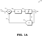
- FIGs 1A , 1B , and 2 illustrate sigma-delta modulators and a corresponding output characteristic of a 1-bit quantizer with a limited regeneration time that operate as the basis of continuous-time sigma-delta modulators depicted in FIGs. 3-8.
- FIGs. 3 - 8 illustrate systems and techniques that are used to reduce metastability error in a continuous-time sigma-delta analog-to-digital converter (ADC) of a data processor.
- a dual-feedback technique is used in combination with dual quantization to reduce the metastability error of the data processor and address the delay that occurs in each feedback loop of the dual-feedback system.
- the dual-feedback technique includes a pair of digital-to-analog converters (DAC) that are configured to compensate for the delay in a quantizer of each feedback loop of the data processor.
- DAC digital-to-analog converters
- FIG. 1A illustrates a block diagram of a sigma-delta modulator 100.
- the sigma-delta modulator 100 is an example of a data processor with a feedback system.
- the sigma-delta modulator 100 includes an adder 112, a loop filter (H(s)) 102, a quantizer or analog-to-digital converter (ADC) 104, and a digital-to-analog converter (DAC) 106.
- the DAC 106 provides a feedback path to adder 112 that is coupled to receive an analog input and the output of the DAC 106.
- An input U 110 is coupled to a positive input of the adder 112.
- the output of the adder 112 is coupled to an input of the loop filter 102.
- the output of the loop filter 102 is coupled to an input of the quantizer 104.
- An output of the quantizer 104 is the output V 114 of the sigma-delta modulator 100.
- the output of the quantizer 104 is also coupled to an input of the DAC 106.
- the output of the DAC 106 is coupled to a negative input of the adder 112 to provide a feedback signal 107. In this way, the DAC 106 is in the feedback path.
- the quantizer 104 and the DAC 106 are both clocked by a clock signal 108 that has a sampling frequency fs. Typically, the sampling frequency may be higher than the minimum required Nyquist rate such that the sigma-delta modulator 100 is oversampled.
- the quantization error of the sigma-delta modulator 100 in the signal band of interest is shaped (approximately) according to the inverse of the loop filter 102 characteristic. Also, the quantization error of the quantizer 104 is suppressed in the frequency region where the gain of the loop filter 102 is high. At frequencies where the gain of the loop filter 102 decreases, the quantization noise increases. However, a digital decimation filter (not shown) can be placed at the output of the sigma-delta modulator 100 to filter out the out-of-band quantization noise.
- sigma-delta modulator 100 is a feedback system, it can become increasingly difficult to keep the sigma-delta modulator 100 stable at high sampling frequencies. This may be due to parasitic poles and any additional delays in the circuit, for example caused by the quantizer 104 and/or DAC 106.
- Another aspect of the sigma-delta modulator 100 (and also the sigma-delta modulator depicted in FIG. 3 ) is that metastability of the quantizer 104 (and similarly quantizer 304) can cause errors in the system, particularly for very small input signals to the quantizer, which can degrade performance, as discussed below with reference to FIGS. 1A through 4 .
- quantizer 104 should provide enough gain to enable a digital decision to be made based on a very small signal received from the loop filter 102.
- the required gain of the quantizer 104 can be, for example, on the order of 10 7 -10 8 .
- the delay of the quantizer 104 has a direct impact on the stability of the sigma-delta loop.
- the time taken by the quantizer 105 to perform the steps of sampling the input and providing output is limited because the regeneration time is part of the total loop delay for the feedback loop, as shown in FIG.
- the total loop delay is normally no more than one sampling clock period.
- the regeneration time of the quantizer is limited, and normally less than one sampling clock period. Indeed, for very high-speed sigma-delta modulators (for example at 10 GHZ to 20 GHz), the maximum allowable delay time of the quantizer 104 may be only 50 ps.
- the achievable gain of the quantizer 104 is directly related to its available time budget, as discussed with regard to equations 1 and 2 and FIG. 1B below.
- an output value provided by the quantizer should conform to one of a number of permissible, or legal, output values.
- the example below is described with reference to a 1-bit quantizer.
- the legal output values in this example are 1 and -1.
- a latch may be used to sense an input signal and to provide an output signal as a logical value (1 or -1).
- Legal logical values that are at the saturated levels (1 or-1) may be referred to as full-scale values.
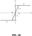
- FIG. 1B shows a profile of an output voltage V out against an input voltage Vinfor a 1-bit quantizer with a limited regeneration time. Limiting the regeneration time has the effect that the gain of the latch is also constrained.
- the output of the quantizer may not reach a full-scale value (legal output 1 or-1), but instead fall at a value between the legal values (e.g. 0.39 or -0.92).
- FIG. 1B shows a profile of an output voltage V out against an input voltage Vinfor a 1-bit quantizer with a limited regeneration time and having the transfer function of Equation 2.
- the output voltage V out increases linearly in a region 150 between 0 V and a voltage representing logical 1 (a full-scale value) as the input voltage V in varies between 0 V and one over the gain of the latch (1/G).
- the output voltage V out is saturated in a region 152 at the voltage representing logical 1.
- the output voltage V out increases linearly in a region 154 between 0 V and a voltage representing logical -1 (a full-scale value) as the input voltage V in varies between 0 V and minus one over the gain of the latch (-1/G). Where the input voltage Vinis more negative than minus one over the gain of the latch (-1/G), the output voltage V out is saturated 156 at the voltage representing logical -1.
- the quantizer output V 114 is the input of the DAC 106.
- the DAC 106 can further resolve it and deliver full-scale output in the feedback path to the adder 112. This effect may be referred to as the gain (G DAC ) of the DAC 106.
- the gain (G DAC ) of the DAC 106 is also limited, and may be substantially lower than the gain of the quantizer (G q ).
- the sampled quantizer output is not full-scale.
- the (not full-scale) output V 114 of the sigma-delta modulator 100 is typically provided to external digital processing circuitry (not shown).
- the thresholding and gain applied by the digital processing circuitry has the effect of forcing the output V 114 to a full-scale value.
- the output of the sigma-delta modulator therefore appears to take a valid digital value from the perspective of down-stream digital electronics.
- the output of the DAC 106 may also not take a full-scale value (-1 or 1), but instead fall at some number between -1 and 1, even after considering the gain of the DAC 106.
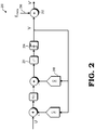
- FIG. 2 illustrates a schematic block diagram of a data processor 200.
- the data processor 200 comprises a sigma-delta modulator similar to the sigma-delta modulator described previously with reference to FIG. 1A , but includes a delay block 231 associated with the delay of quantizer 204 and the delay of DAC 248.
- An output V of the sigma-delta modulator is provided to adder 202.
- the metastability error (E meta ) 290 may be considered as being introduced by adder 202, as the output V of the quantizer 204 is forced to a full-scale value V', as shown in FIG. 2 .
- FIG. 3 illustrates a block diagram of a data processor 300 utilizing a metastability error compensation technique according to various embodiments.
- the data processor 300 includes an adder 312, a digital-to-analog converter (DAC) 346, a loop filter (H(s)) 323, and a metastability error compensation module 381.
- the metastability error compensation module 381 includes an adder 313, an adder 311, a quantization or analog-to-digital conversion (ADC) module 320, a digital-to-analog converter (DAC) 348, a quantization or analog-to-digital conversion (ADC) module 321, and a digital-to-analog converter (DAC) 347.
- ADC analog-to-digital conversion
- DAC digital-to-analog converter
- the quantization module 320 includes a delay block 331 and a quantizer or analog-to-digital converter (ADC) 304.
- the quantization module 321 includes a delay block 332 and a quantizer 305.
- the data processor 300 includes a first quantization module 320 and a second quantization module 321 as part of a metastability error compensation circuit.
- the metastability error compensation circuit may be extended to include an additional quantizer or a plurality of quantizers with corresponding feedback loops and DACS configured to compensate for the metastability error and the delay caused by the additional quantizers.
- an input U 310 is coupled to a positive input of the adder 312.
- the output of the adder 312 is coupled to an input of the loop filter (H(s)) 323.
- the output of the loop filter (H(s)) 323 is coupled to an input of the adder 313.
- the adder 313 of error compensation module 381 receives the analog output 391 from loop filter 323 and the analog full-scale output 357 from DAC 347.
- DAC 347 is configured to convert digital output V' 397 from a digital signal to an analog signal.
- the adder 313 subtracts the analog full-scale output 357 from the analog output 391.
- Analog output 357, provided to adder 313 from DAC 347 is the analog version of the digital output voltage V' 397 that is provided as the output of quantizer 305.
- the output of adder 313 (analog output 392), is provided to adder 311 along with analog output 358 from DAC 348.
- the adder 311 of first feedback loop 382 receives the analog output 392 from the adder 313 and analog output 358 from DAC 348.
- the analog output 358 that is provided to adder 311 from DAC 348 is the analog version of the digital output V 395 that is provided as the output of quantizer 304.
- Adder 311 subtracts the analog output 358 from the analog output 392 to obtain analog output 393, which is provided to quantization module 320.
- Quantization module 320 associated with the first feedback loop 382, receives analog output 393.
- the delay block 331 of quantization module 320 is indicative of the delay associated with quantizer 304 and DAC 348.
- DAC 348 converts the digital output of quantizer 304 of quantization module 320 from digital to analog.
- the total delay including, for example, the quantizer delay, the DAC delay, and the propagation delay from the quantizer to the DAC, should be less or equal to one sampling clock period (Ts) of the sigma-elta modulator.
- Ts sampling clock period
- DAC 348 each compensate for the excess loop delay (ELD) in their corresponding feedback loops (e.g., first feedback loop 382 and second feedback loop 383).
- ELD is defined as the total loop delay that includes, for example, the comparator regeneration time of the quantizers, propagation delay from each quantizer to each DAC (from quantizer 304 to DAC 348 and from quantizer 305 to DAC 347), and the delay of the DAC 347 and DAC 348 in each loop.
- subtracting the analog output 358 from the analog output 392 compensates for the delay of the quantizer 304, the propagation delay to the DAC 348, and the delay of DAC 348.
- subtracting the analog output 357 from the analog output 391 compensates for the delay of the quantizer 305, the propagation delay to the DAC 347, and the delay of DAC 347.
- the ELD (which includes the regeneration time of each comparator) is not negligible compared with the sampling clock period (Ts) of the sigma-delta ADC and therefore is rectified using DAC 348 and DAC 347.
- the ELD for high-speed sigma-delta ADCs such as, for example, the quantizers 304 and 305 of data processor 300, is compensated for in order to avoid the detrimental effects of the ELDs, which include, for example, a decreased signal-to-quantization-noise-ratio (SQNR) or an unstable sigma-delta modulator (i.e., the ELD causes the sigma-delta demodulator to become unstable).
- SQNR signal-to-quantization-noise-ratio
- an unstable sigma-delta modulator i.e., the ELD causes the sigma-delta demodulator to become unstable.
- data processor 300 compensates for ELD by implementing a direct feedback loop around each quantizer (first feedback loop 382 for quantizer 332 and second feedback loop 383 for quantizer 305) using the DACs (DAC 348 and 347). That is, the ELD compensation is implemented using, for example, the direct feedback loop around each quantizer through DAC 348 and DAC 347. As depicted in FIG. 3 , one sampling clock period ELD (indicated as z -1 in the z-domain) for each feedback loop is compensated for using the DAC 348 and DAC 347. Thus, a total delay of two clock periods is compensated for using DAC 348 and DAC 347.
- quantizer 304 receives and quantizes the output of adder 311 to generate output V 395.
- the output V 395 provided at the output of quantizer 304 may be a single voltage representative of a single bit or it may be a plurality of voltages representative of a respective plurality of bits, depending on the configuration of the quantizer 304.
- the quantizer 304 may be an m-bit (where m-bit means m bits in thermometer/unary code, not m bits in binary code) quantizer (m > 2) comprising m-1 pre-amplifiers and m-1 latches, as is known in the art.
- the pre-amplifiers compare the input of the quantizer 304 with a series of references (which may be reference voltages or reference currents, for example).
- the latches act on the respective outputs of the pre-amplifiers to provide output signals that represent digital values of the respective m-bits.
- the output V 395 may include a metastability error, where the output does not conform to a full-scale value due to the input conditions of the quantizer 304 during at least some clock cycles. That is, as discussed previously with reference to the quantizer in FIG. 1A , ideally, the output of the quantizer 304 should take on full-scale output values of -1 or +1 volts.
- the sampled quantizer output is generally not at full-scale values resulting in metastability error, which is, as previously described, the difference between the actual output V 395 (e.g., -0.92) and the full-scale value of output V' 397 (e.g., -1).
- the output V 395 is provided to quantization module 321.
- Quantization module 321 of second feedback loop 383 receives digital output V 395 from quantizer 304. That is, quantizer 304 provides output V 396 to quantizer 305 for metastability error correction.
- Quantizer 305 receives the output of quantizer 304 at its input and corrects the metastability error associated with the output V 395. In order to correct the metastability error at the output V 395, the quantizer 305 receives the output V 396 at its input and provides a digital, full-scale output V' 397 at its output. By passing the output V 396 through the quantizer 305, the output V 395 is effectively forced to a full-scale value (a saturated, legal logic value). The reason for this is that the quantizer 305 has further gain, which may be the same gain as the quantizer 304, and so the probability of the "full-scale" output V' 397 not taking a full-scale value is reduced by a factor of the gain.
- full-scale quantizer 305 refers to the objective of the quantizer and that there may be a non-zero probability that the output of the "full-scale” quantizer 305 does not fall at a full-scale value.
- the quantizer 305 may differ from the quantizer 304 in that pre-amplifiers may be omitted in the quantizer 305. That is, the quantizer 305 might comprise only m-1 latches. Reference values for the latches of the quantizer 305 may be taken to be the same as those for the quantizer 304. In this case, every latch of the quantizer 305 samples the output of a corresponding latch of the quantizer 304 of the quantization model. Regeneration is performed by the quantizer 305 from these latched values.
- the quantizer 305 may comprise fewer latches than the quantizer 304.
- the latch(es) of the quantizer 304 with output that may contain a quantization error are determined dynamically (as is known in the art) and only the output of those latches are re-quantized by the quantizer 305, similar to the approach used in a tracking quantizer.
- Both the output V 395 of the quantizer 304 and the output V' 397 of the quantizer 305 are converted to analog values using DAC 348 and DAC 347, respectively.
- the DAC 348 receives the output V 395 of the quantizer 304 and provides an analog output 358 to adder 311.
- the DAC 347 receives the full-scale output V' 397 of the quantizer 305 and provides a full-scale analog output 357 to adder 313.
- the adder 311 receives the analog output 392 and the analog output 358.
- the adder 313 receives the analog output 391 and the analog full-scale output 357 from DAC 347.
- the DAC 347 receives the full-scale output V' 397 of the quantizer 305 and provides a full-scale analog output 357.
- the DAC 348 provides the first feedback loop 382 to adder 311 to perform a delay compensation.
- the first feedback loop 382 from quantizer 304 of quantization module 320 has an output voltage V 395 that is fed back to the input of quantization module 320 through DAC 348.
- First feedback loop 382 is a first order feedback loop and is considered the inner ELD compensation loop.
- the DAC 347 provides the second feedback loop 383 to adder 313 to perform the second delay compensation.
- the second feedback loop 383 from quantizer 305 of quantization module 321 has the output V' 397 that is fed back to quantizer 320 input through DAC 347, adder 313, and adder 311.
- the second feedback loop 383 is a second order feedback loop and is referred to as the outer ELD compensation loop.
- the second feedback loop 383 that performs the second delay compensation includes the first delay compensation performed by the first feedback loop 382, thus accounting for the total delay compensation in both the first feedback loop 382 and the second feedback loop 383. That is, the second feedback loop 383 is configured to account for the total delay compensation that occurs in the entire data processor 300.
- the third feedback loop 384 feeds the output of quantization module 321 through DAC 346 and is the main feedback loop of the sigma-delta modulator that has a stringent requirement on the total quantization gain.
- FIG. 4 illustrates the quantization noise and metastability error of the sigma-delta ADC depicted in FIG. 2 in accordance with at least one embodiment.
- FIG. 5 illustrates the quantization noise and metastability error of the sigma-delta ADC associated with the metastability error compensation module 381 of data processor 300 in accordance with at least one embodiment.
- 1-bit quantizers quantizers 304 and 305 are utilized for the sigma-delta ADC, however, similar results occur for sigma-delta ADCs that utilize multi-bit quantizers.
- FIGs. 4 and 5 show a profile of an output voltage V out against an input voltage Vinfor a 1-bit quantizer with a limited generation time.
- line 410 represents the output characteristic of the quantizer 304 in the sigma-delta modulator of FIG. 3 without the metastability shaping technique shown in FIG. 3 .
- the area 425 is the metastability error which is denoted as E meta .
- the metastability error occurs with a probability of 1/(G q1 ⁇ G DAC ).
- the power of the metastability error is lower than the quantization noise.
- the quantization noise is in the sigma-delta loop and shaped by the noise transfer function of the quantizer 304.
- the metastability error that is present at the output of the sigma-delta modulator is located directly at the output of the quantizer, which is not shaped.
- the power of the metastability error seems to be very low, however, it can still cause dramatic degradation on the overall performance of the sigma-delta ADCs.
- FIG. 5 depicts the diagram of the quantization noise and the metastability error of the sigma-delta ADC with metastability shaping technique shown in FIG. 3 .
- the line 510 is the overall output characteristic of the first quantizer (quantizer 304) and the second quantizer (quantizer 305) including the DAC gains (DAC 348 and DAC 347).
- the area 515 is the quantization error of the quantizer 304 without the additional quantizer 305.
- the area 530 is the quantization noise of the second quantizer (quantizer 305).
- the output of DAC 348 has metastability error, and the output of the DAC 346 and DAC 347 do not have metastability error (or have relatively low metastability error) because of the additional quantizer gain G q2 of the second quantizer (quantizer 305).
- the metastability error occurs with a probability of 1/(G q1 ⁇ G q2 ⁇ G DAC ), which is G q2 times lower than the conventional sigma-delta ADC.
- FIG. 6 illustrates the noise transfer functions associated with quantizer 304 and quantizer 305 of FIG. 3 compared to an ideal noise transfer function according to various embodiments.
- Both of the quantization noises, q 1 and q 2 , of quantizer 304 and quantizer 305, respectively, are shaped by a full-order noise transfer function, as depicted in FIG. 6 .
- full-order means the same order as the loop filter 323 of FIG. 3 .
- the line 610 shows the ideal noise transfer function (NTF) of the conventional sigma-delta modulator.
- the dotted line 615 depicts the actual NTF of the quantization noise q 1 of the quantizer 304, which approximates to the ideal NTF.
- the dashed line 620 depicts the actual NTF of the quantization noise q 2 of the quantizer 305.
- the in-band part of the actual NTF of the quantization noise q 2 is overlapped with the ideal NTF, while the high-frequency portion of the actual NTF displays a minor difference, as can be seen in FIG. 6 .
- the out-of-band gain of the actual NTF of the quantization noise q 2 is slightly higher than the ideal NTF, but does not impact the stability of the sigma-delta modulator, because the power of the quantization noise q 2 of quantizer 305 is much lower than the quantization noise q 1 of quantizer 304.
- FIG. 7 illustrates a method 700 of operating a data processor using metastability error compensation according to various embodiments.
- an analog signal (analog output 392) is received at first feedback loop 382.
- DAC 348 is used to compensate for a first excess loop delay (ELD) that is associated with the first quantizer 304.
- ELD excess loop delay
- the first quantizer output 395 is provided to the second quantizer 305.
- the second quantizer output (output V 397) is provided to the DAC 347 of the second feedback loop 383.
- the DAC 347 of the second feedback loop 383 is used to compensate for the second ELD associated with the quantizer 305 and the second DAC 347.
- the metastability error associated with the first quantizer output (output V 395) is reduced using the second quantizer 305.
- a voltage output (output V' 397) is provided at the output of data processor 300 with a reduced metastability error.
- FIG. 8 illustrates a method 800 of operating a data processor using metastability error compensation according to various embodiments.
- an analog signal (analog output 392) is received at the first feedback loop 382.
- the first quantization noise q 1 (depicted in FIG. 5 ) of quantizer 304 associated with first feedback loop 382 is generated.
- a second quantization noise q 2 of a second quantizer 305 associated with second feedback loop 383 is generated.
- the second quantization noise q 2 of the second quantizer 305 is used to shape a first metastability error E meta associated with the output of the first quantizer 304 (output V 395).
- a voltage output (output V' 397) is provided at the output of data processor 300 with a reduced metastability error.
- loop filter 323 in FIG. 3 is depicted using a feed-forward structure
- other structures including, for example, a feedback structure or a combined feed-forward / feedback structure may be utilized for the metastability shaping technique depicted in FIG. 3 .
- a 1-bit quantizer has been chosen to present the metastability shaping technique
- multi-bit quantizers may also be used for metastability shaping technique depicted in FIG. 3 .
- a multi-stage noise shaping (MASH) sigma-delta modulator or cascaded sigma-delta modulator may be used as the sigma-delta modulator depicted in FIG. 3 .
- MASH multi-stage noise shaping
- a method includes using a first feedback loop to compensate for a first excess loop delay (ELD) associated with a first quantizer and a first DAC of the first feedback loop.
- the first quantizer provides a first quantizer output to a second feedback loop.
- a second feedback loop compensates for a second ELD associated a second quantizer and a second DAC of the second feedback loop.
- the second quantizer reduces a metastability error associated with the first quantizer output.
Landscapes
- Engineering & Computer Science (AREA)
- Theoretical Computer Science (AREA)
- Compression, Expansion, Code Conversion, And Decoders (AREA)
Abstract
Description
- Sigma-delta analog-to-digital converters (ADCs) are used in modern data processors to generate high-speed data. Metastability error is a type of error that occurs at the output of a sigma-delta ADC when the voltage output of a quantizer that is used to convert the analog signal to a digital signal is not at the ideal voltage output expected by the data processor. Not addressing the detrimental effects of metastability error may result in a data processor that is inaccurate. Thus, there exists a need to provide corrective techniques that address the effects of metastability error in a data processor.
- Aspects of the disclosure are defined in the accompanying claims.
- In a first aspect, there is provided a method, comprising: using a first feedback loop to compensate for a first excess loop delay (ELD) associated with a first quantizer; and providing a first quantizer output of the first quantizer to a second feedback loop, the second feedback loop compensating for a second ELD associated with a second quantizer, the second quantizer reducing a metastability error associated with the first quantizer output.
- In one or more embodiments, a first digital-to-analog converter (DAC) output provided by a first DAC of the first feedback loop may be configured to compensate for a first quantizer delay; and a second DAC output provided by a second DAC of the second feedback loop may be configured to compensate for a second quantizer delay.
- In one or more embodiments, the method may further comprise feeding the output of the second quantizer through a third DAC of a third feedback loop, the third feedback loop having a total quantization gain requirement.
- In one or more embodiments, the method may further comprise: converting the first quantizer output of the first quantizer to an analog signal using the first DAC; and converting a second quantizer output of the second quantizer to a second analog signal using the second DAC.
- In one or more embodiments, the method may further comprise converting the second quantizer output of the second quantizer to a third analog signal using a third DAC.
- In one or more embodiments, the method may further comprising using a third adder to subtract the third analog signal from a first input to the third adder.
- In one or more embodiments, the method may further comprise subtracting a first DAC output from a second feedback loop adder output using a first feedback loop adder.
- In one or more embodiments, the method may further comprise: subtracting a first DAC output from a second feedback loop adder output using a first feedback loop adder; and subtracting a second DAC output from a loop filter output to generate the second feedback loop adder output.
- In a second aspect, there is provided an apparatus, comprising: a first feedback loop having a first digital-to-analog-converter (DAC) coupled to a first quantizer; and a second feedback loop having a second DAC coupled to a second quantizer, wherein the first DAC is coupled to the first quantizer to compensate for a first excess loop delay (ELD), the second DAC is coupled to the second quantizer to compensate for a second excess loop delay (ELD), and the second quantizer reduces a metastability error associated with an output of the first quantizer.
- In one or more embodiments, the first ELD may be associated with the first quantizer; and the second ELD may be associated with the second quantizer.
- In one or more embodiments, a first DAC output provided by the first DAC of the first feedback loop may be configured to compensate for a first quantizer delay; and a second DAC output provided by the second DAC may be configured to compensate for a second quantizer delay.
- In one or more embodiments, the apparatus may further comprise a third feedback loop, wherein the output of the second quantizer is fed through a third DAC of the third feedback loop, the third feedback loop having a total quantization gain requirement.
- In one or more embodiments, the total quantization gain requirement may include a first gain of the first quantizer, a second gain of the second quantizer, and a third gain of the third DAC.
- In one or more embodiments, the output of the first quantizer may be converted to an analog signal using the first DAC; and the output of the second quantizer may be converted to a second analog signal using the second DAC.
- In one or more embodiments, the first quantizer and the second quantizer may be at least one of a single-bit or multi-bit quantizer.
- In a third aspect, there is provided a method, comprising: generating a first quantization noise of a first quantizer associated with a first feedback loop; generating, based on the first quantization noise of the first quantizer, a second quantization noise of a second quantizer associated with a second feedback loop; and using the second quantization noise of the second quantizer to shape a first metastability error associated with an output of the first quantizer.
- In one or more embodiments, using the second quantization noise of the second quantizer to shape the first metastability error may comprise subtracting the second quantization noise of the second quantizer from the first metastability error to generate a second metastability error.
- In one or more embodiments, the second metastability error may be a reduced metastability error compared to the first metastability error.
- In one or more embodiments, a first gain of the first quantizer and a second gain of the second quantizer may be used to generate a power of the second quantization noise.
- In one or more embodiments, the second quantizer may be a full-scale quantizer.
- The present disclosure may be better understood, and its numerous features and advantages made apparent to those skilled in the art by referencing the accompanying drawings. The use of the same reference symbols in different drawings indicates similar or identical items.
-
FIG. 1A is a schematic block diagram of a sigma-delta modulator. -
FIG. 1B is an output characteristic of the 1-bit quantizer ofFIG. 1A with a limited regeneration time. -
FIG. 2 illustrates a schematic block diagram of a data processor with metastability error. -
FIG. 3 shows a schematic block diagram of a data processor with a continuous-time sigma-delta ADC having a metastability error compensation module according to various embodiments. -
FIG. 4 illustrates the quantization noise and metastability error of the sigma-delta ADC depicted inFIG. 2 according to various embodiments. -
FIG. 5 illustrates the quantization noise and metastability error of the sigma-delta ADC depicted inFIG. 3 according to various embodiments. -
FIG. 6 illustrates the noise transfer functions associated with the continuous-time sigma-delta ADC with a metastability error compensation module ofFIG. 3 according to various embodiments. -
FIG. 7 illustrates a method of operating a data processor using metastability error compensation according to various embodiments. -
FIG. 8 illustrates a method of operating a data processor using metastability error compensation according to various embodiments. -
FIGs 1A ,1B , and2 illustrate sigma-delta modulators and a corresponding output characteristic of a 1-bit quantizer with a limited regeneration time that operate as the basis of continuous-time sigma-delta modulators depicted inFIGs. 3-8. FIGs. 3 - 8 illustrate systems and techniques that are used to reduce metastability error in a continuous-time sigma-delta analog-to-digital converter (ADC) of a data processor. A dual-feedback technique is used in combination with dual quantization to reduce the metastability error of the data processor and address the delay that occurs in each feedback loop of the dual-feedback system. The dual-feedback technique includes a pair of digital-to-analog converters (DAC) that are configured to compensate for the delay in a quantizer of each feedback loop of the data processor. By applying the metastability error compensation technique using dual-quantization and compensating for the delay of the additional quantizers using the DACs associated with each feedback loop, the data processor is able to reduce the amount of metastability error that occurs at the output of the data processor. -
FIG. 1A illustrates a block diagram of a sigma-delta modulator 100. The sigma-delta modulator 100 is an example of a data processor with a feedback system. The sigma-delta modulator 100 includes anadder 112, a loop filter (H(s)) 102, a quantizer or analog-to-digital converter (ADC) 104, and a digital-to-analog converter (DAC) 106. TheDAC 106 provides a feedback path toadder 112 that is coupled to receive an analog input and the output of theDAC 106. - An
input U 110 is coupled to a positive input of theadder 112. The output of theadder 112 is coupled to an input of theloop filter 102. The output of theloop filter 102 is coupled to an input of thequantizer 104. An output of thequantizer 104 is theoutput V 114 of the sigma-delta modulator 100. In order to provide the feedback loop, the output of thequantizer 104 is also coupled to an input of theDAC 106. The output of theDAC 106 is coupled to a negative input of theadder 112 to provide afeedback signal 107. In this way, theDAC 106 is in the feedback path. Thequantizer 104 and theDAC 106 are both clocked by aclock signal 108 that has a sampling frequency fs. Typically, the sampling frequency may be higher than the minimum required Nyquist rate such that the sigma-delta modulator 100 is oversampled. - Due to the presence of feedback, the
loop filter 102, and the fact that a sigma-delta modulator 100 is usually highly oversampled, the quantization error of the sigma-delta modulator 100 in the signal band of interest is shaped (approximately) according to the inverse of theloop filter 102 characteristic. Also, the quantization error of thequantizer 104 is suppressed in the frequency region where the gain of theloop filter 102 is high. At frequencies where the gain of theloop filter 102 decreases, the quantization noise increases. However, a digital decimation filter (not shown) can be placed at the output of the sigma-delta modulator 100 to filter out the out-of-band quantization noise. - However, as a sigma-
delta modulator 100 is a feedback system, it can become increasingly difficult to keep the sigma-delta modulator 100 stable at high sampling frequencies. This may be due to parasitic poles and any additional delays in the circuit, for example caused by thequantizer 104 and/orDAC 106. Another aspect of the sigma-delta modulator 100 (and also the sigma-delta modulator depicted inFIG. 3 ) is that metastability of the quantizer 104 (and similarly quantizer 304) can cause errors in the system, particularly for very small input signals to the quantizer, which can degrade performance, as discussed below with reference toFIGS. 1A through 4 . - To support reliable operation of the sigma-
delta modulator 100,quantizer 104 should provide enough gain to enable a digital decision to be made based on a very small signal received from theloop filter 102. Depending on the resolution of the sigma-delta modulator 100 and the specified system bit error rate (BER), the required gain of thequantizer 104 can be, for example, on the order of 107-108. However, the delay of thequantizer 104 has a direct impact on the stability of the sigma-delta loop. For a continuous-time sigma-delta ADC, the time taken by the quantizer 105 to perform the steps of sampling the input and providing output is limited because the regeneration time is part of the total loop delay for the feedback loop, as shown inFIG. 1A , and the total loop delay is normally no more than one sampling clock period. The time from thequantizer 104 sampling its input signal, to the next block (DAC 106 or its driving circuits) sampling theoutput V 114 of thequantizer 104, is defined as the regeneration time for the quantizer. The regeneration time of the quantizer is limited, and normally less than one sampling clock period. Indeed, for very high-speed sigma-delta modulators (for example at 10 GHZ to 20 GHz), the maximum allowable delay time of thequantizer 104 may be only 50 ps. The achievable gain of thequantizer 104 is directly related to its available time budget, as discussed with regard toequations FIG. 1B below. - For an ideal quantizer, an output value provided by the quantizer should conform to one of a number of permissible, or legal, output values. For simplicity, the example below is described with reference to a 1-bit quantizer. The legal output values in this example are 1 and -1. A transfer function of the ideal 1-bit quantizer is:

- To implement a quantizer with solid-state circuitry, a latch may be used to sense an input signal and to provide an output signal as a logical value (1 or -1). Legal logical values that are at the saturated levels (1 or-1) may be referred to as full-scale values.
-
FIG. 1B shows a profile of an output voltage Vout against an input voltage Vinfor a 1-bit quantizer with a limited regeneration time. Limiting the regeneration time has the effect that the gain of the latch is also constrained. When an input of a quantizer is very small (close to 0), the output of the quantizer may not reach a full-scale value (legal output 1 or-1), but instead fall at a value between the legal values (e.g. 0.39 or -0.92). The transfer function of the quantizer with limited gain may be express as (assuming the quantizer has a linear gain model):
-
FIG. 1B shows a profile of an output voltage Vout against an input voltage Vinfor a 1-bit quantizer with a limited regeneration time and having the transfer function ofEquation 2. For positive values of the input voltage Vin, the output voltage Vout increases linearly in aregion 150 between 0 V and a voltage representing logical 1 (a full-scale value) as the input voltage Vin varies between 0 V and one over the gain of the latch (1/G). Where the input Vin is greater than one over the gain of the latch (1/G), the output voltage Vout is saturated in aregion 152 at the voltage representing logical 1. Similarly, for negative values of the input voltage Vin, the output voltage Vout increases linearly in aregion 154 between 0 V and a voltage representing logical -1 (a full-scale value) as the input voltage Vin varies between 0 V and minus one over the gain of the latch (-1/G). Where the input voltage Vinis more negative than minus one over the gain of the latch (-1/G), the output voltage Vout is saturated 156 at the voltage representing logical -1. - As discussed previously with regards to
FIG. 1A , thequantizer output V 114 is the input of theDAC 106. In practice, even if the sampled quantizer output is not full-scale, but close to full-scale, theDAC 106 can further resolve it and deliver full-scale output in the feedback path to theadder 112. This effect may be referred to as the gain (GDAC) of theDAC 106. The gain (GDAC) of theDAC 106 is also limited, and may be substantially lower than the gain of the quantizer (Gq). A total loop gain (Gloop) of the sigma-delta modulator can be considered to be the quantizer gain (Gq) multiplied by DAC gain (GDAC):
- If the sampled quantizer input is very small (Vin<1/Gloop), the sampled quantizer output is not full-scale. The (not full-scale)
output V 114 of the sigma-delta modulator 100 is typically provided to external digital processing circuitry (not shown). The thresholding and gain applied by the digital processing circuitry has the effect of forcing theoutput V 114 to a full-scale value. The output of the sigma-delta modulator therefore appears to take a valid digital value from the perspective of down-stream digital electronics. However, for the feedback loop within the sigma-delta modulator 100, the output of theDAC 106 may also not take a full-scale value (-1 or 1), but instead fall at some number between -1 and 1, even after considering the gain of theDAC 106. - The metastability error, Emeta, is defined as the difference between the actual output V 114 (e.g. -0.92) of the sigma-
delta modulator 100 and a corresponding full-scale value V' (e.g. -1):
-
FIG. 2 illustrates a schematic block diagram of adata processor 200. Thedata processor 200 comprises a sigma-delta modulator similar to the sigma-delta modulator described previously with reference toFIG. 1A , but includes adelay block 231 associated with the delay ofquantizer 204 and the delay ofDAC 248. An output V of the sigma-delta modulator is provided to adder 202. The metastability error (Emeta) 290 may be considered as being introduced byadder 202, as the output V of thequantizer 204 is forced to a full-scale value V', as shown inFIG. 2 . -
FIG. 3 illustrates a block diagram of adata processor 300 utilizing a metastability error compensation technique according to various embodiments. Thedata processor 300 includes anadder 312, a digital-to-analog converter (DAC) 346, a loop filter (H(s)) 323, and a metastabilityerror compensation module 381. The metastabilityerror compensation module 381 includes anadder 313, anadder 311, a quantization or analog-to-digital conversion (ADC)module 320, a digital-to-analog converter (DAC) 348, a quantization or analog-to-digital conversion (ADC)module 321, and a digital-to-analog converter (DAC) 347. Thequantization module 320 includes adelay block 331 and a quantizer or analog-to-digital converter (ADC) 304. Thequantization module 321 includes a delay block 332 and a quantizer 305. In various embodiments, thedata processor 300 includes afirst quantization module 320 and asecond quantization module 321 as part of a metastability error compensation circuit. However, in various embodiments, the metastability error compensation circuit (metastability error compensation module 381) may be extended to include an additional quantizer or a plurality of quantizers with corresponding feedback loops and DACS configured to compensate for the metastability error and the delay caused by the additional quantizers. - As is the case for the sigma-
delta modulator 100 ofFIG. 1A , for the sigma-delta modulator ofFIG. 3 , aninput U 310 is coupled to a positive input of theadder 312. The output of theadder 312 is coupled to an input of the loop filter (H(s)) 323. The output of the loop filter (H(s)) 323 is coupled to an input of theadder 313. - The
adder 313 oferror compensation module 381, which is an example of an analog combining circuit, receives theanalog output 391 fromloop filter 323 and the analog full-scale output 357 fromDAC 347. As stated previously,DAC 347 is configured to convert digital output V' 397 from a digital signal to an analog signal. Theadder 313 subtracts the analog full-scale output 357 from theanalog output 391.Analog output 357, provided to adder 313 fromDAC 347, is the analog version of the digital output voltage V' 397 that is provided as the output of quantizer 305. The output of adder 313 (analog output 392), is provided to adder 311 along withanalog output 358 fromDAC 348. - The
adder 311 offirst feedback loop 382 receives theanalog output 392 from theadder 313 andanalog output 358 fromDAC 348. Theanalog output 358 that is provided to adder 311 fromDAC 348 is the analog version of thedigital output V 395 that is provided as the output of quantizer 304.Adder 311 subtracts theanalog output 358 from theanalog output 392 to obtain analog output 393, which is provided toquantization module 320. -
Quantization module 320, associated with thefirst feedback loop 382, receives analog output 393. In various embodiments, thedelay block 331 ofquantization module 320 is indicative of the delay associated with quantizer 304 andDAC 348. - In various embodiments, prior to providing
analog output 358 to adder 311,DAC 348 converts the digital output of quantizer 304 ofquantization module 320 from digital to analog. The total delay, including, for example, the quantizer delay, the DAC delay, and the propagation delay from the quantizer to the DAC, should be less or equal to one sampling clock period (Ts) of the sigma-elta modulator. Thus, thefirst feedback loop 382 compensates for the delay of thequantization module 320. - In various embodiments, DAC 348 (and similarly DAC 347) each compensate for the excess loop delay (ELD) in their corresponding feedback loops (e.g.,
first feedback loop 382 and second feedback loop 383). ELD is defined as the total loop delay that includes, for example, the comparator regeneration time of the quantizers, propagation delay from each quantizer to each DAC (from quantizer 304 toDAC 348 and from quantizer 305 to DAC 347), and the delay of theDAC 347 andDAC 348 in each loop. Thus, subtracting theanalog output 358 from theanalog output 392 compensates for the delay of the quantizer 304, the propagation delay to theDAC 348, and the delay ofDAC 348. Similarly, subtracting theanalog output 357 from theanalog output 391 compensates for the delay of the quantizer 305, the propagation delay to theDAC 347, and the delay ofDAC 347. - For high-speed continuous time sigma-delta ADCs, such as for the
data processor 300 depicted inFIG. 3 , the ELD (which includes the regeneration time of each comparator) is not negligible compared with the sampling clock period (Ts) of the sigma-delta ADC and therefore is rectified usingDAC 348 andDAC 347. That is, the ELD for high-speed sigma-delta ADCs, such as, for example, the quantizers 304 and 305 ofdata processor 300, is compensated for in order to avoid the detrimental effects of the ELDs, which include, for example, a decreased signal-to-quantization-noise-ratio (SQNR) or an unstable sigma-delta modulator (i.e., the ELD causes the sigma-delta demodulator to become unstable). - In various embodiments,
data processor 300 compensates for ELD by implementing a direct feedback loop around each quantizer (first feedback loop 382 for quantizer 332 andsecond feedback loop 383 for quantizer 305) using the DACs (DAC 348 and 347). That is, the ELD compensation is implemented using, for example, the direct feedback loop around each quantizer throughDAC 348 andDAC 347. As depicted inFIG. 3 , one sampling clock period ELD (indicated as z-1 in the z-domain) for each feedback loop is compensated for using theDAC 348 andDAC 347. Thus, a total delay of two clock periods is compensated for usingDAC 348 andDAC 347. - Referring back to quantizer 304, quantizer 304 receives and quantizes the output of
adder 311 to generateoutput V 395. Theoutput V 395 provided at the output of quantizer 304 may be a single voltage representative of a single bit or it may be a plurality of voltages representative of a respective plurality of bits, depending on the configuration of the quantizer 304. For example, the quantizer 304 may be an m-bit (where m-bit means m bits in thermometer/unary code, not m bits in binary code) quantizer (m > 2) comprising m-1 pre-amplifiers and m-1 latches, as is known in the art. The pre-amplifiers compare the input of the quantizer 304 with a series of references (which may be reference voltages or reference currents, for example). The latches act on the respective outputs of the pre-amplifiers to provide output signals that represent digital values of the respective m-bits. Theoutput V 395 may include a metastability error, where the output does not conform to a full-scale value due to the input conditions of the quantizer 304 during at least some clock cycles. That is, as discussed previously with reference to the quantizer inFIG. 1A , ideally, the output of the quantizer 304 should take on full-scale output values of -1 or +1 volts. However, the sampled quantizer output is generally not at full-scale values resulting in metastability error, which is, as previously described, the difference between the actual output V 395 (e.g., -0.92) and the full-scale value of output V' 397 (e.g., -1). Theoutput V 395 is provided toquantization module 321. -
Quantization module 321 ofsecond feedback loop 383 receivesdigital output V 395 from quantizer 304. That is, quantizer 304 providesoutput V 396 to quantizer 305 for metastability error correction. - Quantizer 305 receives the output of quantizer 304 at its input and corrects the metastability error associated with the
output V 395. In order to correct the metastability error at theoutput V 395, the quantizer 305 receives theoutput V 396 at its input and provides a digital, full-scale output V' 397 at its output. By passing theoutput V 396 through the quantizer 305, theoutput V 395 is effectively forced to a full-scale value (a saturated, legal logic value). The reason for this is that the quantizer 305 has further gain, which may be the same gain as the quantizer 304, and so the probability of the "full-scale" output V' 397 not taking a full-scale value is reduced by a factor of the gain. It will be appreciated that the term "full-scale" quantizer 305 refers to the objective of the quantizer and that there may be a non-zero probability that the output of the "full-scale" quantizer 305 does not fall at a full-scale value. - In some examples, the quantizer 305 may differ from the quantizer 304 in that pre-amplifiers may be omitted in the quantizer 305. That is, the quantizer 305 might comprise only m-1 latches. Reference values for the latches of the quantizer 305 may be taken to be the same as those for the quantizer 304. In this case, every latch of the quantizer 305 samples the output of a corresponding latch of the quantizer 304 of the quantization model. Regeneration is performed by the quantizer 305 from these latched values.
- In further examples, the quantizer 305 may comprise fewer latches than the quantizer 304. The latch(es) of the quantizer 304 with output that may contain a quantization error are determined dynamically (as is known in the art) and only the output of those latches are re-quantized by the quantizer 305, similar to the approach used in a tracking quantizer. Both the
output V 395 of the quantizer 304 and the output V' 397 of the quantizer 305 are converted to analogvalues using DAC 348 andDAC 347, respectively. - The
DAC 348 receives theoutput V 395 of the quantizer 304 and provides ananalog output 358 toadder 311. TheDAC 347 receives the full-scale output V' 397 of the quantizer 305 and provides a full-scale analog output 357 toadder 313. Theadder 311 receives theanalog output 392 and theanalog output 358. Similarly, theadder 313 receives theanalog output 391 and the analog full-scale output 357 fromDAC 347. - As stated previously, the
DAC 347 receives the full-scale output V' 397 of the quantizer 305 and provides a full-scale analog output 357. TheDAC 348 provides thefirst feedback loop 382 to adder 311 to perform a delay compensation. Thefirst feedback loop 382 from quantizer 304 ofquantization module 320 has anoutput voltage V 395 that is fed back to the input ofquantization module 320 throughDAC 348.First feedback loop 382 is a first order feedback loop and is considered the inner ELD compensation loop. TheDAC 347 provides thesecond feedback loop 383 to adder 313 to perform the second delay compensation. Thesecond feedback loop 383 from quantizer 305 ofquantization module 321 has the output V' 397 that is fed back toquantizer 320 input throughDAC 347,adder 313, andadder 311. Thesecond feedback loop 383 is a second order feedback loop and is referred to as the outer ELD compensation loop. - In various embodiments, the
second feedback loop 383 that performs the second delay compensation includes the first delay compensation performed by thefirst feedback loop 382, thus accounting for the total delay compensation in both thefirst feedback loop 382 and thesecond feedback loop 383. That is, thesecond feedback loop 383 is configured to account for the total delay compensation that occurs in theentire data processor 300. Thethird feedback loop 384 feeds the output ofquantization module 321 throughDAC 346 and is the main feedback loop of the sigma-delta modulator that has a stringent requirement on the total quantization gain. -
FIG. 4 illustrates the quantization noise and metastability error of the sigma-delta ADC depicted inFIG. 2 in accordance with at least one embodiment.FIG. 5 illustrates the quantization noise and metastability error of the sigma-delta ADC associated with the metastabilityerror compensation module 381 ofdata processor 300 in accordance with at least one embodiment. For the examples depicted inFIGs. 4 and 5 , 1-bit quantizers (quantizers 304 and 305) are utilized for the sigma-delta ADC, however, similar results occur for sigma-delta ADCs that utilize multi-bit quantizers.FIGs. 4 and 5 show a profile of an output voltage Vout against an input voltage Vinfor a 1-bit quantizer with a limited generation time. - With reference to
FIG. 4 ,line 410 represents the output characteristic of the quantizer 304 in the sigma-delta modulator ofFIG. 3 without the metastability shaping technique shown inFIG. 3 . Thearea 415 between theline 410 and the line 420 (i.e., the line where Vout = Vin) is the quantization error of the quantizer 304, which is also called quantization noise denoted as q1. Thearea 425 is the metastability error which is denoted as Emeta. For the sigma-delta ADC associated withFIG. 4 , the metastability error occurs with a probability of 1/(Gq1·GDAC). Then, if assuming the input to quantizer 304 is uniformly distributed in the defined input swing (-1, 1), the probability density function of the metastability error is

- The power of the metastability error (area 425) from the original sigma-delta modulator may be calculated as

- Similarly, the probability density function of the quantization noise q1 of the quantizer 304 in the sigma-delta modulator is

- The power of the quantization noise of the quantizer in the sigma-delta modulator q1 can be calculated as

- Even with relatively low total loop quantizer gain Gq1·GDAC (e.g., 40 dB), the power of the metastability error is lower than the quantization noise. However, the quantization noise is in the sigma-delta loop and shaped by the noise transfer function of the quantizer 304. Thus, the in-band quantization noise in the final output is suppressed. The metastability error that is present at the output of the sigma-delta modulator is located directly at the output of the quantizer, which is not shaped. As a result, the power of the metastability error seems to be very low, however, it can still cause dramatic degradation on the overall performance of the sigma-delta ADCs.
-
FIG. 5 depicts the diagram of the quantization noise and the metastability error of the sigma-delta ADC with metastability shaping technique shown inFIG. 3 . Theline 510 is the overall output characteristic of the first quantizer (quantizer 304) and the second quantizer (quantizer 305) including the DAC gains (DAC 348 and DAC 347). Thearea 515 is the quantization error of the quantizer 304 without the additional quantizer 305. Thearea 530 is the quantization noise of the second quantizer (quantizer 305). - In various embodiments, when the input voltage of the quantizer 304 is within (1/(Gq1·Gq2·GDAC), 1/(Gq1·GDAC)) or (-1/(Gq1·GDAC), -1/(Gq1·Gq2·GDAC)), the output of
DAC 348 has metastability error, and the output of theDAC 346 andDAC 347 do not have metastability error (or have relatively low metastability error) because of the additional quantizer gain Gq2 of the second quantizer (quantizer 305). Thus, at the output ofDAC 346, the metastability error occurs with a probability of 1/(Gq1·Gq2·GDAC), which is Gq2 times lower than the conventional sigma-delta ADC. The power of the metastability error E'meta at the output of theDAC 346 can be calculated as

- The probability density function of the quantization noise q2 of the second quantizer (quantizer 305) is

- The power of the quantization noise of the quantizer 305 is

- The metastability error Emeta, depicted in
Fig. 4 , may now be divided into two parts, q2 and E'meta, with reference to the sigma-delta ADC ofFIG. 3 with metastability error compensation module 381:
-
FIG. 6 illustrates the noise transfer functions associated with quantizer 304 and quantizer 305 ofFIG. 3 compared to an ideal noise transfer function according to various embodiments. Both of the quantization noises, q1 and q2, of quantizer 304 and quantizer 305, respectively, are shaped by a full-order noise transfer function, as depicted inFIG. 6 . As it relates to the noise transfer functions, full-order means the same order as theloop filter 323 ofFIG. 3 . Theline 610 shows the ideal noise transfer function (NTF) of the conventional sigma-delta modulator. The dottedline 615 depicts the actual NTF of the quantization noise q1 of the quantizer 304, which approximates to the ideal NTF. The dashedline 620 depicts the actual NTF of the quantization noise q2 of the quantizer 305. The in-band part of the actual NTF of the quantization noise q2 is overlapped with the ideal NTF, while the high-frequency portion of the actual NTF displays a minor difference, as can be seen inFIG. 6 . The out-of-band gain of the actual NTF of the quantization noise q2 is slightly higher than the ideal NTF, but does not impact the stability of the sigma-delta modulator, because the power of the quantization noise q2 of quantizer 305 is much lower than the quantization noise q1 of quantizer 304. -
FIG. 7 illustrates amethod 700 of operating a data processor using metastability error compensation according to various embodiments. With reference toFIG. 3 , atblock 710, an analog signal (analog output 392) is received atfirst feedback loop 382. Atblock 720,DAC 348 is used to compensate for a first excess loop delay (ELD) that is associated with the first quantizer 304. Atblock 725, thefirst quantizer output 395 is provided to the second quantizer 305. Atblock 730, the second quantizer output (output V 397) is provided to theDAC 347 of thesecond feedback loop 383. Atblock 740, theDAC 347 of thesecond feedback loop 383 is used to compensate for the second ELD associated with the quantizer 305 and thesecond DAC 347. Atblock 750, the metastability error associated with the first quantizer output (output V 395) is reduced using the second quantizer 305. Atblock 760, a voltage output (output V' 397) is provided at the output ofdata processor 300 with a reduced metastability error. -
FIG. 8 illustrates amethod 800 of operating a data processor using metastability error compensation according to various embodiments. With reference toFIGs. 3 and5 , atblock 810, an analog signal (analog output 392) is received at thefirst feedback loop 382. Atblock 820, the first quantization noise q1 (depicted inFIG. 5 ) of quantizer 304 associated withfirst feedback loop 382 is generated. Atblock 830, based on the first quantization noise, a second quantization noise q2 of a second quantizer 305 associated withsecond feedback loop 383 is generated. At block 840, the second quantization noise q2 of the second quantizer 305 is used to shape a first metastability error Emeta associated with the output of the first quantizer 304 (output V 395). Atblock 850, a voltage output (output V' 397) is provided at the output ofdata processor 300 with a reduced metastability error. - In various embodiments, although the
loop filter 323 inFIG. 3 is depicted using a feed-forward structure, other structures including, for example, a feedback structure or a combined feed-forward / feedback structure may be utilized for the metastability shaping technique depicted inFIG. 3 . Also, although a 1-bit quantizer has been chosen to present the metastability shaping technique, multi-bit quantizers may also be used for metastability shaping technique depicted inFIG. 3 . In various embodiments, a multi-stage noise shaping (MASH) sigma-delta modulator or cascaded sigma-delta modulator may be used as the sigma-delta modulator depicted inFIG. 3 . - A method includes using a first feedback loop to compensate for a first excess loop delay (ELD) associated with a first quantizer and a first DAC of the first feedback loop. The first quantizer provides a first quantizer output to a second feedback loop. A second feedback loop compensates for a second ELD associated a second quantizer and a second DAC of the second feedback loop. The second quantizer reduces a metastability error associated with the first quantizer output.
- Note that not all of the activities or elements described above in the general description are required, that a portion of a specific activity or device may not be required, and that one or more further activities may be performed, or elements included, in addition to those described. Still further, the order in which activities are listed are not necessarily the order in which they are performed. Also, the concepts have been described with reference to specific embodiments. However, one of ordinary skill in the art appreciates that various modifications and changes can be made without departing from the scope of the present disclosure as set forth in the claims below. Accordingly, the specification and figures are to be regarded in an illustrative rather than a restrictive sense, and all such modifications are intended to be included within the scope of the present disclosure.
- Benefits, other advantages, and solutions to problems have been described above with regard to specific embodiments. However, the benefits, advantages, solutions to problems, and any feature(s) that may cause any benefit, advantage, or solution to occur or become more pronounced are not to be construed as a critical, required, or essential feature of any or all the claims. Moreover, the particular embodiments disclosed above are illustrative only, as the disclosed subject matter may be modified and practiced in different but equivalent manners apparent to those skilled in the art having the benefit of the teachings herein. No limitations are intended to the details of construction or design herein shown, other than as described in the claims below. It is therefore evident that the particular embodiments disclosed above may be altered or modified and all such variations are considered within the scope of the disclosed subject matter. Accordingly, the protection sought herein is as set forth in the claims below.
Claims (15)
- A method, comprising:using a first feedback loop to compensate for a first excess loop delay (ELD) associated with a first quantizer;providing a first quantizer output of the first quantizer to a second feedback loop, the second feedback loop compensating for a second ELD associated with a second quantizer, the second quantizer reducing a metastability error associated with the first quantizer output.
- The method of claim 1, wherein:a first digital-to-analog converter (DAC) output provided by a first DAC of the first feedback loop is configured to compensate for a first quantizer delay; anda second DAC output provided by a second DAC of the second feedback loop is configured to compensate for a second quantizer delay.
- The method of any preceding claim, further comprising:
feeding the output of the second quantizer through a third DAC of a third feedback loop, the third feedback loop having a total quantization gain requirement. - The method of any preceding claim, further comprising:converting the first quantizer output of the first quantizer to an analog signal using the first DAC; andconverting a second quantizer output of the second quantizer to a second analog signal using the second DAC.
- The method of claim 4, further comprising:
converting the second quantizer output of the second quantizer to a third analog signal using a third DAC. - The method of claim 5, further comprising:
using a third adder to subtract the third analog signal from a first input to the third adder. - The method of any preceding claim, further comprising:
subtracting a first DAC output from a second feedback loop adder output using a first feedback loop adder. - The method of any preceding claim, further comprising:subtracting a first DAC output from a second feedback loop adder output using a first feedback loop adder; andsubtracting a second DAC output from a loop filter output to generate the second feedback loop adder output.
- An apparatus, comprising:a first feedback loop having a first digital-to-analog-converter (DAC) coupled to a first quantizer;a second feedback loop having a second DAC coupled to a second quantizer, wherein the first DAC is coupled to the first quantizer to compensate for a first excess loop delay (ELD), the second DAC is coupled to the second quantizer to compensate for a second excess loop delay (ELD), and the second quantizer reduces a metastability error associated with an output of the first quantizer.
- The apparatus of claim 9, wherein:the first ELD is associated with the first quantizer; andthe second ELD is associated with the second quantizer.
- The apparatus of claim 10, wherein:a first DAC output provided by the first DAC of the first feedback loop is configured to compensate for a first quantizer delay; anda second DAC output provided by the second DAC is configured to compensate for a second quantizer delay.
- The apparatus of claim 11, further comprising:
a third feedback loop, wherein the output of the second quantizer is fed through a third DAC of the third feedback loop, the third feedback loop having a total quantization gain requirement. - The apparatus of claim 12, wherein:
the total quantization gain requirement includes a first gain of the first quantizer, a second gain of the second quantizer, and a third gain of the third DAC. - The apparatus of claim 13, wherein:the output of the first quantizer is converted to an analog signal using the first DAC; andthe output of the second quantizer is converted to a second analog signal using the second DAC.
- The apparatus of claim 14, wherein:
the first quantizer and the second quantizer are at least one of a single-bit or multi-bit quantizer.
Applications Claiming Priority (1)
| Application Number | Priority Date | Filing Date | Title |
|---|---|---|---|
| US16/407,501 US10763888B1 (en) | 2019-05-09 | 2019-05-09 | Metastability shaping technique for continuous-time sigma-delta analog-to-digital converters |
Publications (1)
| Publication Number | Publication Date |
|---|---|
| EP3736988A1 true EP3736988A1 (en) | 2020-11-11 |
Family
ID=70470908
Family Applications (1)
| Application Number | Title | Priority Date | Filing Date |
|---|---|---|---|
| EP20171605.7A Ceased EP3736988A1 (en) | 2019-05-09 | 2020-04-27 | Metastability shaping technique for continuous-time sigma-delta analog-to-digital converters |
Country Status (3)
| Country | Link |
|---|---|
| US (1) | US10763888B1 (en) |
| EP (1) | EP3736988A1 (en) |
| CN (1) | CN111917417A (en) |
Families Citing this family (8)
| Publication number | Priority date | Publication date | Assignee | Title |
|---|---|---|---|---|
| US11444632B2 (en) * | 2020-10-22 | 2022-09-13 | Infineon Technologies Austria Ag | Tracking analog-to-digital converter for power converters |
| EP4040682B1 (en) * | 2021-02-05 | 2025-07-02 | Imec VZW | An analog-to-digital converter circuitry, an integrated circuit device, a photoplethysmogram detector, a wearable device and a method for analog-to-digital conversion |
| US11967967B2 (en) * | 2022-06-17 | 2024-04-23 | Nxp B.V. | Signal shaping for compensation of metastable errors |
| US12015426B2 (en) * | 2022-08-04 | 2024-06-18 | Nxp B.V. | System and method of reducing delta-sigma modulator error using force-and-correction |
| CN116052731B (en) * | 2023-01-18 | 2026-01-27 | 福州大学 | Multi-bit quantization method for memory |
| DE102023203900A1 (en) * | 2023-04-27 | 2024-10-31 | Robert Bosch Gesellschaft mit beschränkter Haftung | Sigma-Delta Modulator and Method for Operating a Sigma-Delta Modulator |
| US20260066919A1 (en) * | 2024-09-04 | 2026-03-05 | Nxp B.V. | High-Speed Continuous-Time Delta-Sigma Modulator Including an Amplifier with Limited Gain |
| US20260066918A1 (en) * | 2024-09-04 | 2026-03-05 | Nxp B.V. | Continuous-Time Delta-Sigma Modulator with Capacitive Feed-ins |
Family Cites Families (16)
| Publication number | Priority date | Publication date | Assignee | Title |
|---|---|---|---|---|
| US7173980B2 (en) * | 2002-09-20 | 2007-02-06 | Ditrans Ip, Inc. | Complex-IF digital receiver |
| US6836228B1 (en) * | 2002-11-20 | 2004-12-28 | Xicor, Inc. | Analog-to-digital converter with switched integrator |
| JP2005295494A (en) * | 2003-12-25 | 2005-10-20 | Matsushita Electric Ind Co Ltd | DC offset cancel circuit |
| US7446687B2 (en) * | 2006-10-27 | 2008-11-04 | Realtek Semiconductor Corp. | Method and apparatus to reduce internal circuit errors in a multi-bit delta-sigma modulator |
| US7636056B2 (en) * | 2007-05-22 | 2009-12-22 | Panasonic Corporation | Delta sigma modulator operating with different power source voltages |
| GB2452524A (en) * | 2007-09-06 | 2009-03-11 | Cambridge Silicon Radio Ltd | A jitter insensitive sigma-delta modulator |
| US7880654B2 (en) * | 2009-02-27 | 2011-02-01 | Freescale Semiconductor, Inc. | Continuous-time sigma-delta modulator with multiple feedback paths having independent delays |
| US8319674B2 (en) * | 2010-09-11 | 2012-11-27 | Dialog Semiconductor Gmbh | Compensation of loop-delay quantizer in continuous-time and hybrid sigma-delta analog-to-digital modulators |
| EP2802077B1 (en) | 2013-05-10 | 2015-07-08 | Nxp B.V. | A sigma-delta modulator |
| CN104954018B (en) * | 2014-03-28 | 2018-03-27 | 澜起科技(上海)有限公司 | ∑ Δ analog-digital converter |
| US9166617B1 (en) * | 2014-03-31 | 2015-10-20 | Freescale Semiconductor, Inc. | Communication unit, digital band-pass sigma-delta modulator and method therefor |
| US9722626B2 (en) * | 2015-01-05 | 2017-08-01 | General Electric Company | Method and system using computational sigma-delta modulators |
| KR102384362B1 (en) * | 2015-07-17 | 2022-04-07 | 삼성전자주식회사 | Delta sigma modulator for shaping noise and audio codec having the same |
| KR101742131B1 (en) * | 2016-10-17 | 2017-05-31 | 성균관대학교산학협력단 | Delta-sigma modulator |
| EP3340475B1 (en) | 2016-12-22 | 2021-04-28 | Nxp B.V. | Metastability compensation |
| EP3413468A1 (en) * | 2017-06-08 | 2018-12-12 | Nxp B.V. | A sigma delta modulator, integrated circuit and method therefor |
-
2019
- 2019-05-09 US US16/407,501 patent/US10763888B1/en active Active
-
2020
- 2020-04-27 EP EP20171605.7A patent/EP3736988A1/en not_active Ceased
- 2020-05-08 CN CN202010384709.1A patent/CN111917417A/en active Pending
Non-Patent Citations (5)
| Title |
|---|
| CHAO CHU: "A High Speed/High Linearity Continuous-Time Delta-Sigma Modulator DISSERTATION to obtain the acadamic degree", 1 January 2017 (2017-01-01), XP055723617, Retrieved from the Internet <URL:https://oparu.uni-ulm.de/xmlui/bitstream/handle/123456789/4597/Dissertation_Chu_v1.pdf?sequence=3&isAllowed=y> [retrieved on 20200819] * |
| KELLER M ET AL: "A Comparative Study on Excess-Loop-Delay Compensation Techniques for Continuous-Time Sigma-Delta Modulators", IEEE TRANSACTIONS ON CIRCUITS AND SYSTEMS I: REGULAR PAPERS, IEEE, US, vol. 53, no. 11, 1 December 2008 (2008-12-01), pages 3480 - 3487, XP011227272, ISSN: 1549-8328 * |
| VENKATESH SRINIVASAN ET AL: "A 20mW 61dB SNDR (60MHz BW) 1b 3 rd -order continuous-time delta-sigma modulator clocked at 6GHz in 45nm CMOS", SOLID-STATE CIRCUITS CONFERENCE DIGEST OF TECHNICAL PAPERS (ISSCC), 2012 IEEE INTERNATIONAL, IEEE, 19 February 2012 (2012-02-19), pages 158 - 160, XP032154411, ISBN: 978-1-4673-0376-7, DOI: 10.1109/ISSCC.2012.6176958 * |
| VIKAS SINGH ET AL: "Compensating for Quantizer Delay in Excess of One Clock Cycle in Continuous-Time delta\Sigma Modulators", IEEE TRANSACTIONS ON CIRCUITS AND SYSTEMS II: EXPRESS BRIEFS, IEEE, USA, vol. 57, no. 9, 1 September 2010 (2010-09-01), pages 676 - 680, XP011318487, ISSN: 1549-7747 * |
| ZHANG CHENMING: "Broadband Continuous-time MASH Sigma-Delta ADCs", 21 September 2021 (2021-09-21), XP055919767, ISBN: 978-90-38-65322-8, Retrieved from the Internet <URL:https://pure.tue.nl/ws/portalfiles/portal/182349223/20210921_Zhang_Chenming_hf.pdf> [retrieved on 20220510] * |
Also Published As
| Publication number | Publication date |
|---|---|
| US10763888B1 (en) | 2020-09-01 |
| CN111917417A (en) | 2020-11-10 |
Similar Documents
| Publication | Publication Date | Title |
|---|---|---|
| US10763888B1 (en) | Metastability shaping technique for continuous-time sigma-delta analog-to-digital converters | |
| US7522079B1 (en) | Sigma-delta modulator with DAC resolution less than ADC resolution and increased tolerance of non-ideal integrators | |
| US11770126B2 (en) | Noise-shaping enhanced gated ring oscillator based analog-to-digital converters | |
| US8120518B2 (en) | Digital feedforward sigma-delta modulator in analog-to-digital converter and modulation method thereof | |
| US7450047B1 (en) | Sigma-delta modulator with DAC resolution less than ADC resolution and increased dynamic range | |
| US7535392B2 (en) | Delta sigma modulator and method for compensating delta sigma modulators for loop delay | |
| US7525464B2 (en) | Sigma-delta modulator with DAC resolution less than ADC resolution | |
| US20110032132A1 (en) | Delta-sigma analog-to-digital conversion apparatus and method thereof | |
| US9143158B2 (en) | Sigma-delta modulator | |
| EP3252953B1 (en) | Analog-to-digital converter with embedded noise-shaped truncation, embedded noise-shaped segmentation and/or embedded excess loop delay compensation | |
| US7439889B2 (en) | AD converter | |
| US7564391B2 (en) | Sigma delta modulator summing input, reference voltage, and feedback | |
| US7446687B2 (en) | Method and apparatus to reduce internal circuit errors in a multi-bit delta-sigma modulator | |
| US6914549B2 (en) | Reconfigurable analog-to-digital converter | |
| US10979069B2 (en) | Delta-sigma modulator with truncation error compensation and associated method | |
| CN104980154A (en) | Estimation of digital-to-analog converter static mismatch errors | |
| US10014878B1 (en) | Metastability compensation | |
| US10432214B2 (en) | Apparatus for applying different transfer functions to code segments of multi-bit output code that are sequentially determined and output by multi-bit quantizer and associated delta-sigma modulator | |
| US11870453B2 (en) | Circuits and methods for a noise shaping analog to digital converter | |
| US7557744B2 (en) | PWM driver and class D amplifier using same | |
| US12489457B2 (en) | Continuous-time data converter with digital multi-stage noise shaping subconverter | |
| CN114079471A (en) | Multilevel Sigma-Delta Analog-to-Digital Converter with Dithering | |
| JP2004274606A (en) | Modulator | |
| EP2157700B1 (en) | Delta-sigma analog-to-digital converter circuit and method for analog-to-digital converting | |
| CN117278030A (en) | noise shaping variable quantizer |
Legal Events
| Date | Code | Title | Description |
|---|---|---|---|
| PUAI | Public reference made under article 153(3) epc to a published international application that has entered the european phase |
Free format text: ORIGINAL CODE: 0009012 |
|
| STAA | Information on the status of an ep patent application or granted ep patent |
Free format text: STATUS: THE APPLICATION HAS BEEN PUBLISHED |
|
| AK | Designated contracting states |
Kind code of ref document: A1 Designated state(s): AL AT BE BG CH CY CZ DE DK EE ES FI FR GB GR HR HU IE IS IT LI LT LU LV MC MK MT NL NO PL PT RO RS SE SI SK SM TR |
|
| AX | Request for extension of the european patent |
Extension state: BA ME |
|
| STAA | Information on the status of an ep patent application or granted ep patent |
Free format text: STATUS: REQUEST FOR EXAMINATION WAS MADE |
|
| 17P | Request for examination filed |
Effective date: 20210511 |
|
| RBV | Designated contracting states (corrected) |
Designated state(s): AL AT BE BG CH CY CZ DE DK EE ES FI FR GB GR HR HU IE IS IT LI LT LU LV MC MK MT NL NO PL PT RO RS SE SI SK SM TR |
|
| STAA | Information on the status of an ep patent application or granted ep patent |
Free format text: STATUS: EXAMINATION IS IN PROGRESS |
|
| 17Q | First examination report despatched |
Effective date: 20220224 |
|
| STAA | Information on the status of an ep patent application or granted ep patent |
Free format text: STATUS: THE APPLICATION HAS BEEN REFUSED |
|
| 18R | Application refused |
Effective date: 20241019 |