EP3736955A1 - Method and system for control of tunable passive component based power filters - Google Patents
Method and system for control of tunable passive component based power filters Download PDFInfo
- Publication number
- EP3736955A1 EP3736955A1 EP19212436.0A EP19212436A EP3736955A1 EP 3736955 A1 EP3736955 A1 EP 3736955A1 EP 19212436 A EP19212436 A EP 19212436A EP 3736955 A1 EP3736955 A1 EP 3736955A1
- Authority
- EP
- European Patent Office
- Prior art keywords
- terminal
- passive component
- tunable
- switching device
- voltage
- Prior art date
- Legal status (The legal status is an assumption and is not a legal conclusion. Google has not performed a legal analysis and makes no representation as to the accuracy of the status listed.)
- Withdrawn
Links
Images



Classifications
-
- H—ELECTRICITY
- H02—GENERATION; CONVERSION OR DISTRIBUTION OF ELECTRIC POWER
- H02M—APPARATUS FOR CONVERSION BETWEEN AC AND AC, BETWEEN AC AND DC, OR BETWEEN DC AND DC, AND FOR USE WITH MAINS OR SIMILAR POWER SUPPLY SYSTEMS; CONVERSION OF DC OR AC INPUT POWER INTO SURGE OUTPUT POWER; CONTROL OR REGULATION THEREOF
- H02M3/00—Conversion of DC power input into DC power output
- H02M3/02—Conversion of DC power input into DC power output without intermediate conversion into AC
- H02M3/04—Conversion of DC power input into DC power output without intermediate conversion into AC by static converters
- H02M3/10—Conversion of DC power input into DC power output without intermediate conversion into AC by static converters using discharge tubes with control electrode or semiconductor devices with control electrode
- H02M3/145—Conversion of DC power input into DC power output without intermediate conversion into AC by static converters using discharge tubes with control electrode or semiconductor devices with control electrode using devices of a triode or transistor type requiring continuous application of a control signal
- H02M3/155—Conversion of DC power input into DC power output without intermediate conversion into AC by static converters using discharge tubes with control electrode or semiconductor devices with control electrode using devices of a triode or transistor type requiring continuous application of a control signal using semiconductor devices only
- H02M3/156—Conversion of DC power input into DC power output without intermediate conversion into AC by static converters using discharge tubes with control electrode or semiconductor devices with control electrode using devices of a triode or transistor type requiring continuous application of a control signal using semiconductor devices only with automatic control of output voltage or current, e.g. switching regulators
- H02M3/158—Conversion of DC power input into DC power output without intermediate conversion into AC by static converters using discharge tubes with control electrode or semiconductor devices with control electrode using devices of a triode or transistor type requiring continuous application of a control signal using semiconductor devices only with automatic control of output voltage or current, e.g. switching regulators including plural semiconductor devices as final control devices for a single load
-
- H—ELECTRICITY
- H02—GENERATION; CONVERSION OR DISTRIBUTION OF ELECTRIC POWER
- H02M—APPARATUS FOR CONVERSION BETWEEN AC AND AC, BETWEEN AC AND DC, OR BETWEEN DC AND DC, AND FOR USE WITH MAINS OR SIMILAR POWER SUPPLY SYSTEMS; CONVERSION OF DC OR AC INPUT POWER INTO SURGE OUTPUT POWER; CONTROL OR REGULATION THEREOF
- H02M1/00—Details of apparatus for conversion
- H02M1/14—Arrangements for reducing ripples from DC input or output
-
- H—ELECTRICITY
- H03—ELECTRONIC CIRCUITRY
- H03J—TUNING RESONANT CIRCUITS; SELECTING RESONANT CIRCUITS
- H03J1/00—Details of adjusting, driving, indicating, or mechanical control arrangements for resonant circuits in general
- H03J1/0008—Details of adjusting, driving, indicating, or mechanical control arrangements for resonant circuits in general using a central processing unit, e.g. a microprocessor
-
- H—ELECTRICITY
- H02—GENERATION; CONVERSION OR DISTRIBUTION OF ELECTRIC POWER
- H02J—ELECTRIC POWER NETWORKS; CIRCUIT ARRANGEMENTS OR SYSTEMS FOR SUPPLYING OR DISTRIBUTING ELECTRIC POWER; SYSTEMS FOR STORING ELECTRIC ENERGY
- H02J1/00—Circuit arrangements for DC mains or DC distribution networks
- H02J1/02—Arrangements for reducing harmonics or ripples
-
- H—ELECTRICITY
- H02—GENERATION; CONVERSION OR DISTRIBUTION OF ELECTRIC POWER
- H02J—ELECTRIC POWER NETWORKS; CIRCUIT ARRANGEMENTS OR SYSTEMS FOR SUPPLYING OR DISTRIBUTING ELECTRIC POWER; SYSTEMS FOR STORING ELECTRIC ENERGY
- H02J2105/00—Networks for supplying or distributing electric power characterised by their spatial reach or by the load
- H02J2105/30—Networks for supplying or distributing electric power characterised by their spatial reach or by the load the load networks being external to vehicles, i.e. exchanging power with vehicles
- H02J2105/32—Networks for supplying or distributing electric power characterised by their spatial reach or by the load the load networks being external to vehicles, i.e. exchanging power with vehicles for aircrafts
-
- H—ELECTRICITY
- H03—ELECTRONIC CIRCUITRY
- H03H—IMPEDANCE NETWORKS, e.g. RESONANT CIRCUITS; RESONATORS
- H03H7/00—Multiple-port networks comprising only passive electrical elements as network components
- H03H7/01—Frequency selective two-port networks
- H03H7/0115—Frequency selective two-port networks comprising only inductors and capacitors
-
- H—ELECTRICITY
- H03—ELECTRONIC CIRCUITRY
- H03H—IMPEDANCE NETWORKS, e.g. RESONANT CIRCUITS; RESONATORS
- H03H7/00—Multiple-port networks comprising only passive electrical elements as network components
- H03H7/01—Frequency selective two-port networks
- H03H7/0153—Electrical filters; Controlling thereof
-
- Y—GENERAL TAGGING OF NEW TECHNOLOGICAL DEVELOPMENTS; GENERAL TAGGING OF CROSS-SECTIONAL TECHNOLOGIES SPANNING OVER SEVERAL SECTIONS OF THE IPC; TECHNICAL SUBJECTS COVERED BY FORMER USPC CROSS-REFERENCE ART COLLECTIONS [XRACs] AND DIGESTS
- Y02—TECHNOLOGIES OR APPLICATIONS FOR MITIGATION OR ADAPTATION AGAINST CLIMATE CHANGE
- Y02B—CLIMATE CHANGE MITIGATION TECHNOLOGIES RELATED TO BUILDINGS, e.g. HOUSING, HOUSE APPLIANCES OR RELATED END-USER APPLICATIONS
- Y02B70/00—Technologies for an efficient end-user side electric power management and consumption
- Y02B70/10—Technologies improving the efficiency by using switched-mode power supplies [SMPS], i.e. efficient power electronics conversion e.g. power factor correction or reduction of losses in power supplies or efficient standby modes
Definitions
- the present disclosure relates generally to passive power filters and, more particularly, to passive LC filter components circuits such as employed in pulse-width modulated (PWM) drives and power converters.
- PWM pulse-width modulated
- Switched mode DC to DC converter power supplies are widely used to convert power from a source, such as mains power, to DC power supply for electronic devices.
- Switched mode DC to DC converters generally include buck, boost, buck-boost, fly-back, push-pull and forward converter topologies.
- the DC to DC converter commonly employ large passive components for filtering of switching voltage and current ripple to provide the DC output voltage or current with ripple and noise levels within acceptable thresholds.
- resonant filters with narrow-band high attenuation (high Q) at the PWM switching frequency of the converter can be significantly smaller than the conventional low-pass filters which are generally employed for filtering noise and ripple.
- the quality factor of such resonant filter tank is usually set to be high.
- the effective bandwidth is very narrow and centered around the switching or PWM frequency.
- the high attenuation at a specific frequency cannot easily be maintained. This in turn, will cause the resonant filter to lose its high attenuation near the frequency of interest, which in turn, degrades its performance.
- SMPS switched mode power supply
- Also described herein is a method of controlling a tunable passive component in a pulse width modulation controlled switched mode power supply (SMPS) having a power input and an output with tunable passive component power filter.
- the method includes operably connecting and supplying power relative to a circuit ground to a DC bus, converting a voltage on the DC bus to an output voltage by operating a first switching device and a second switching device at a selected frequency, and filtering the output voltage with a tunable output filter, the tunable output filter including a tunable passive component responsive to a control function circuit configured to automatically tune the tunable passive component value based on a voltage associated with operation of the power supply to maintain resonance of the tunable output filter at about the selected frequency.
- SMPS pulse width modulation controlled switched mode power supply
- further embodiments of the system may include that the first switching device having a third terminal and the second switching device having a third terminal, wherein the third terminal of the first switching device is connected to a controller and the third terminal of the second switching device of is connected to the controller, the controller operable to implement PWM control at the selected frequency to control a voltage of the output of the power supply.
- control function circuit configured to automatically tune the passive component value operates independently of the controller implementing PWM control of the first switching device and the second switching device.
- control function circuit configured to automatically tune the passive component value exhibits a bandwidth that is lower than a bandwidth of the controller implementing PWM control of the first switching device and the second switching device.
- control function circuit includes at least a detector operable to sense a voltage applied to the tunable component, a controller operable to formulate a bias voltage based at least in part on the voltage applied to the tunable passive component, and a driver configured apply a voltage to the first control input and a second control input of the tunable passive component based on the bias voltage to automatically tune the tunable passive component value.
- control function circuit includes a controller implementing a proportional-integral control to formulate the bias voltage and thereby tune the tunable passive component value.
- further embodiments of the system may include a capacitor having a first terminal and a second terminal, the first terminal operably to the output of the power supply and the second terminal connected to ground, wherein the capacitor provides at least one of voltage filtering, voltage stability, ripple reduction and improved hold up time for the voltage or current supplied to the output.
- further embodiments of the system may include that at least one of the first switching device and the second switching device is at least one of a metal-oxide-semiconductor field-effect transistor (MOSFET), a FET, a bipolar junction transistor, and an insulated gate bipolar transistor.
- MOSFET metal-oxide-semiconductor field-effect transistor
- further embodiments of the system may include a tunable input filter configured responsive to a voltage of the input power and the voltage associated with the DC bus.
- further embodiments of the system may include that the tunable input filter including a third inductor having a first terminal and a second terminal, the first terminal operably connected to the DC bus, a fourth inductor in series with the third inductor having a first terminal and a second terminal, the first terminal of the fourth inductor operably connected to the second terminal of the third inductor, the second terminal of the fourth inductor operably connected to first terminal of the first switching device, a second tunable passive component connected in parallel with the fourth inductor with a first terminal connected to the first terminal of the fourth inductor and a second terminal connected to the second terminal of the fourth inductor, the second tunable passive component having a first control input and a second control input and a second control function circuit operably connected to the first control input and a second control input, the second control function circuit configured to automatically tune the passive component value based on a voltage associated with the DC bus.
- a method of controlling a tunable passive component in a PWM controlled switched mode power supply (SMPS) having a power input and an output with tunable passive component power filter includes operably connecting and supplying power relative to a circuit ground to a DC bus, converting a voltage on the DC bus to an output voltage by operating a first switching device and a second switching device at a selected frequency, and filtering the output voltage with a tunable output filter, the tunable output filter including a tunable passive component responsive to a control function circuit configured to automatically tune the tunable passive component value based on a voltage associated with operation of the power supply to maintain resonance of the tunable output filter at about the selected frequency.
- SMPS PWM controlled switched mode power supply
- further embodiments of the method may include implementing a PWM control at the selected frequency to control a voltage of the output of the power supply with the first switching device.
- further embodiments of the method may include operating the control function circuit configured to automatically tune the passive component independently of the controller implementing PWM control of the first switching device and the second switching device.
- further embodiments of the method may include configuring the control function circuit configured to automatically tune the passive component value with a bandwidth that is lower than a bandwidth of the controller implementing PWM control of the first switching device and the second switching device.
- further embodiments of the method may include detecting a voltage applied to the tunable passive component, formulating a bias voltage based at least in part on the voltage applied to the tunable passive component, and applying a voltage to control the tunable passive component based on the bias voltage to automatically tune the tunable passive component value.
- further embodiments of the method may include implementing a proportional-integral control in the control function circuit to formulate the bias voltage and thereby tune the tunable passive component value.
- further embodiments of the method may include filtering the output voltage with a capacitor, wherein the capacitor provides at least one of voltage filtering, voltage stability, ripple reduction and improved hold up time for the voltage or current supplied to the output.
- further embodiments of the method may include filtering the input voltage with a tunable input filter responsive to a voltage of the input power and the voltage associated with the DC bus.
- further embodiments of the method may include filtering the input voltage with a tunable input filter, the tunable input filter including a second tunable passive component responsive to a second control function circuit configured to automatically tune the tunable passive component value based on a voltage associated with the DC bus.
- SMPS switched mode power supply
- the SMPS including a DC bus supplied by an power input relative to a circuit ground, an input filter device operable to stabilize the DC bus, and a first switching device operably connected to the DC bus.
- the SMPS also includes a second switching device operably connected to the first switching device and the circuit ground, the first switching device and the second switching device operable at a selected frequency to generate an output voltage of the power supply and a tunable output filter having a tunable passive component operably connected to the tunable passive component, the control function circuit configured to automatically tune the tunable passive component value based on a voltage associated with operation of the power supply to maintain resonance of the tunable output filter at about the selected frequency.
- controller refers to processing circuitry that may include an application specific integrated circuit (ASIC), an electronic circuit, an electronic processor (shared, dedicated, or group) and memory that executes one or more software or firmware programs, a combinational logic circuit, and/or other suitable interfaces and components that provide the described functionality.
- ASIC application specific integrated circuit
- processor shared, dedicated, or group
- memory that executes one or more software or firmware programs, a combinational logic circuit, and/or other suitable interfaces and components that provide the described functionality.
- connection can include an indirect “connection” and/or a direct “connection”.
- embodiments herein relate to an application of a dc-dc converter technique that overcomes the losses incurred as a result of the snubber circuit and reduces power loss in power sensitive or higher efficiency applications such as in an airborne environment.
- the described embodiments are is explained with an embodiment of flyback / forward DC-DC converters, which produces buck and boost topology output with a resonant tunable output voltage filter. While the embodiments herein are describe with reference to a flyback and forward converter DC-to DC converter topology, the embodiments may readily be applied to DC to DC converters with step-up and step-down configurations as well as AC to DC converters in switched mode PWM controlled applications.
- the described embodiments are directed by way of example to converter topology with an integrated controller for tunable passive component based (capacitor or inductor) resonant filters. The controller can automatically tune the passive component value (e.g., capacitor value) to achieve the desired performances under varying operating conditions.
- the controller integrates the sensing, feed-back, PI controller and driver into a single operational amplifier, which greatly reduce the size and power consumption.
- the tunable resonant filter for a power converter as described herein can successfully achieve high attenuation filtering operation at a target frequency under a wide variety of changing operating conditions. Such very high attenuation capability at specific frequency is very beneficial to design filter component of significantly much lower values. This allows to significantly reduce the filter component size, reduce the losses, and improve the dynamic performances of the system.
- Aircraft 10 includes one or more control systems shown generally as 12.
- the control system 12 may include a power system 13 that interconnects with one or more controllers referred to generally as 16 and more specifically as 161, 16r commonly located at or near each engine 141, 14r.
- Other controllers 16 are also be depicted in this instance as 16a, 16b, and the like.
- the reference numerals are annotated with an "1" or “r” to denote the left or right side of the aircraft 10, respectively, for the purpose of simplicity of description.
- the annotation "a”, “b”, ... "n” is employed to simplify designation of a multiple enumeration of a component or element.
- Each of the controllers 16 may be configured to receive various sensor signals from sensors referred to generally as 18 and individually as 18a, 18b, ...18n all over the aircraft 10 and may also operate one or more actuators shown generally as 20, and more specifically as 20a, 20b, 20c, ...20n to control the operation of the engines 14r, 141, flight controls, (not shown), power systems 13 and the like.
- the control system 12 and power system 13 may also be operably connected to various other components throughout the aircraft 10, including, but not limited to other controllers 16, control panels 23, displays 25, and the like.
- controllers 16 e.g., 16a may also be configured to receive power from various aircraft sources, e.g., generators, batteries and the like and distribute power as needed to various systems in the aircraft 10
- the power system 13 may be part of a controller 16.
- the configuration could be the opposite with the controller 16 operating as or providing a portion of the power system 13, as illustrated by the general depiction of 16a and described further herein.
- the power system 13 includes a power supply (or converter) 100 hereinafter referred to as a power supply 100 as described herein for receiving power from a bus system, converting and routing power to various components in the aircraft 10.
- a power supply 100 may be a single or three-phase AC to DC converter, or it could be a DC to DC converter.
- the power supply 100 is a DC to DC converter.
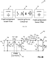
- FIG 2A depicts a simplified block diagram of a switching power converter or power supply 50.
- the switching power supply 50 may include an input filter section 52, switching converter section 54, and an output filter section 56.
- the filter sections may be fully passive, typically low-pass or resonant circuits.
- FIG. 2B depicts a more detailed example of a portion of a power supply 100 in a flyback or forward converters DC to DC configuration.
- the topology of the power supply facilitates producing buck and boost DC outputs, though in the topology depicted a buck converter is shown for example.
- the power supply 100 receives power at a power input 102 from a power source and a DC bus 104 supported by a filter capacitor 106.
- the power supply 100 employs at least a first switching device 120.
- a first terminal 122a of the first switching device 120 is connected to the DC bus 104 and a second terminal 122b connected to a first terminal 132a of the second switching device 130.
- a second terminal 132b of the second switching device 130 is connected to ground.
- the first switching device 122 and the second switching device 132 are MOSFETS, however other kinds of semiconductor switches are possible including transistors, BJT, IGBT, FETS, and the like.
- a third terminal 122c of the first switching device 120 is connected to a control circuit 140, and a third terminal 132c of the second switching device is connected to the control circuit 140 for implementing PWM control to control the output voltage of the power supply 100.
- the power supply 100 also includes.
- the second terminal 122b of the first switching device 120 and the first terminal 132a of the second switching device 130 is connected to a first terminal 162a of inductor 160 while the second terminal 162b is connected to the first terminal 172a of a second inductor 170.
- the second terminal 172b of the second inductor 170 is connect to the output 196 of the power supply 100.
- a capacitor 172 (C2) is connected in parallel with the second inductor 170 with a first terminal 176a connected to the first terminal 172a of the second inductor 170 and the second terminal 176b connected to the second terminal 172b of the second inductor 170 and thereby the output 196.
- Inductor 170 and capacitor 174 establish a resonant tank circuit. It should be appreciated that while FIG. 2B shows specific configuration of such resonant filters as a parallel combination of inductor 170 and capacitor 174 many other combinations are possible. For example the resonant circuit can be realized in other combinations, such as in series resonance and with a larger number of components and tunable components.
- An output capacitor 190 is connected across the output 196 and provides filtering and stabilization of the load voltage.
- the output capacitor 190 has a first terminal 192a connected to the positive terminal 197a of the output of the power supply 100 and a second terminal 197b of the output capacitor 190 is connected to ground (or at least the lower potential terminal 199b of the output 196.
- FIG 3A depicts a simplified block diagram of a switching power converter or power supply 200 in accordance with an embodiment.
- the switching power converter or power supply 200 may include a input filter section 152, switching converter section 154, and a output filter section 156.
- the input filter section 152 and the output filter section 156 may be configured as tunable filter sections in one embodiment and may be implemented as resonant circuits having a tunable component in accordance with an embodiment. It should be appreciated that while in the described embodiments are directed to the details of a output filter 156, they are equally applicable to the tunable input filter 152 where the controls are based on the input voltage and the voltage on the DC bus.
- FIG. 3B depicts a more detailed example of a portion of a power supply 200 and a description of the power supply 200 with the tunable variable reactance in accordance with an embodiment.
- the topology of the power supply is similar to the power supply 100 except as described herein and facilitates producing buck and boost DC outputs, though in the topology depicted a buck converter is shown for example.
- the power supply 200 receives input power from a power source at a power input 102 and a DC bus 104 supported by a filter capacitor 106.
- the power supply 200 employs at least a first switching device 120.
- a first terminal 122a of the first switching device 120 is connected to the DC bus 104 and a second terminal 122b connected to a first terminal 132a of the second switching device 130.
- a second terminal 132b of the second switching device 130 is connected to ground.
- the first switching device 122 and the second switching device 132 are MOSFETS, however other kinds of semiconductor switches are possible including transistors, BJT, IGBT, FETS, and the like.
- a third terminal 122c of the first switching device 120 is connected to a control circuit 140, and a third terminal 132c of the second switching device is connected to the control circuit 140 for implementing PWM control to control the output voltage of the power supply 200.
- the second terminal 122b of the first switching device 120 and the first terminal 132a of the second switching device 130 is connected to a first terminal 162a of inductor 160 while the second terminal 162b is connected to the first terminal 172a of a second inductor 170.
- the second terminal 172b of the second inductor 170 is connect to the output 196 of the power supply 200.
- a tunable passive component 180 is connected in parallel with the second inductor 170 with a first control terminal 182a connected to the first terminal 172a of the second inductor 170 and a second control terminal 182b connected to the second terminal 172b of the second inductor 170 and thereby the output 196.
- Tunable passive component 180 also includes a first control input 184a and a second control input 184b operably connected to a control function circuit 150.
- the tunable passive component 180 could be a variable capacitor or a variable inductor.
- the capacitance varies as a function of the bias voltage applied between the first control terminal 182a and the second control terminal 182b.
- the value of the capacitance can be tuned over arrange of about 100% to 50%, for a range of 0% to 100% bias voltage, though other values and ranges are possible.
- control function circuit 150 includes a controller 153 executing a control law for controlling the variable capacitor 180 and a detector 155 for sensing the voltage applied to the tunable passive component 180.
- the control function circuit 150 also includes a driver 158 operably connected to the controller 153 and the first control input 184a and the second control input 184b of the tunable passive component 180.
- the tunable passive component 180 is a variable capacitor in one embodiment. Details of the operation of the control function circuit 150 and the controller 152 are provided herein.
- An output capacitor 190 is connected across the output 196 and provides filtering and stabilization of the load voltage.
- the output capacitor 190 has a first terminal 192a connected to the positive terminal 199a of the output of the power supply 100 and a second terminal 192b of the output capacitor 190 is connected to ground (or at least the lower potential terminal 199b of the output 196.
- the control function circuit 150 includes an integrated controller 152 for the tunable passive component 180 based (e.g., capacitor or inductor) resonant filters.
- the controller 153 can automatically tune the passive component 180 value (e.g. capacitor value) to achieve the desired performances under varying operating conditions.
- control function circuit 150 employs detector 155 for sensing voltages and/or currents, a controller 153 implemented as a proportional-integral (PI) controller and a driver 158 configured to interface to the tunable passive component 180 (whether a variable capacitor or variable inductor).
- PI proportional-integral
- driver 158 configured to interface to the tunable passive component 180 (whether a variable capacitor or variable inductor).
- the detector 155, controller 153, and driver 158 may all be integrated into a single amplifier, which greatly reduces size and power consumption.
- the peak of the tank voltage can be utilized as a feedback parameter as an indicator of the resonant tank operation and is sensed by the detector 155.
- the error between a reference voltage and the sensed tank voltage peak is provided as input to the controller 153 for estimation of a reference bias voltage, denoted vbias_ref that is required for actively tuning the tunable passive component 180, (e.g., a resonant tank capacitor).
- the controller 153 output is provided to a driver stage 158 for driving the tunable passive component 180 (e.g., a tunable capacitor) with a bias signal vbias .
- PI controller for the operation of the controller 153, such description is merely illustrative and should not be considered limiting.
- Other control topologies are possible and envisioned including, but not limited to, proportional, proportional-derivative, and proportional-integral-derivative.
- the control diagram in FIG. 4 may operate independently from the main controller (for controlling the power supply (not shown)) by utilizing simple but robust PI controller 153 based scheme.
- the bandwidth of the control scheme for active tuning may, in one embodiment, be lower than the main controller of the power supply 200 to avoid any potential interference but it is selected to be fast enough to compensate the slow component variation in the resonant tank components i.e., the tunable passive component 180.
- Control scheme of FIG. 4 in the circuit of FIG. 3 may achieve high attenuation filtering operation at a target frequency under various changing operating conditions.
- Such high attenuation capability at specific frequencies is very beneficial to facilitate design of filter components of significantly lower values.
- this variable resonant filter approach facilitates use of significantly reduced the filter component sizes, exhibiting reduced losses and improves the dynamic performances of the converter/power supply 200.
- a reduction in filter size or the output ripple (with similar components) of the converter/power supply 200 of more than 50% can be achieved versus a conventional LC low pass passive filter.
- the control system implementing the control methodology/circuits described herein can maintain filtering performance over step load changes from full load to a light load (e.g. less than 40% load) as well as other operating conditions that would result in changes in characteristics of the passive components.
- the load step change in the operation was limited by the tunability of the resonant tank components; otherwise it is found that, the active tuning control can successfully maintain the filter performance over the full load range and broad range variations of the load and environmental conditions.
- FIG. 5 a block diagram is shown to provide a description of a method 500 of controlling a tunable passive component 180 in a PWM controlled a switched mode power supply (SMPS) 200 having a power input 102 and an output 196 with tunable passive component power filter 156 ( FIG. 3A ).
- the method 500 initiates a process block 505 with operably connecting and supplying power relative to a circuit ground to a DC bus 104 and stabilizing the DC bus 104 with an input filter device 152 ( FIG 3A ), e.g. filter capacitor 106 as depicted at process block 510.
- SMPS switched mode power supply
- the method 500 also includes converting a voltage on the DC bus 104 to an output voltage by operating a first switching device 120 and a second switching device 130 at a selected frequency as depicted at process block 515. Further, at process block 520 the method 500 includes filtering the output voltage with a tunable output filter 156, the tunable output filter 156 including a tunable passive component 180 responsive to a control function circuit 150 configured to automatically tune the value of the tunable passive component 180 based on a voltage associated with operation of the power supply 200 to maintain resonance of the tunable output filter 156 at about the selected frequency.
Landscapes
- Engineering & Computer Science (AREA)
- Power Engineering (AREA)
- Computer Hardware Design (AREA)
- Microelectronics & Electronic Packaging (AREA)
- Dc-Dc Converters (AREA)
Abstract
Description
- This invention was made with government support under W91 INF-16-2-0010 awarded by DARPA. The government has certain rights in the invention.
- The present disclosure relates generally to passive power filters and, more particularly, to passive LC filter components circuits such as employed in pulse-width modulated (PWM) drives and power converters.
- Switched mode DC to DC converter power supplies are widely used to convert power from a source, such as mains power, to DC power supply for electronic devices. Switched mode DC to DC converters generally include buck, boost, buck-boost, fly-back, push-pull and forward converter topologies. In such cases, the DC to DC converter commonly employ large passive components for filtering of switching voltage and current ripple to provide the DC output voltage or current with ripple and noise levels within acceptable thresholds.
- In some power electronic converters, resonant filters with narrow-band high attenuation (high Q) at the PWM switching frequency of the converter can be significantly smaller than the conventional low-pass filters which are generally employed for filtering noise and ripple. In order to reduce the filter loss and achieve high attenuation, the quality factor of such resonant filter tank is usually set to be high. As such, the effective bandwidth is very narrow and centered around the switching or PWM frequency. However, in fixed component based resonant filters, due to the variation of filter component values under changing operating conditions, such as varying loads or temperatures, variations of resonant tank inductance or capacitance, the high attenuation at a specific frequency cannot easily be maintained. This in turn, will cause the resonant filter to lose its high attenuation near the frequency of interest, which in turn, degrades its performance.
- Accordingly, it is desirable to provide a switched mode power supply or converter output that can successfully achieve high attenuation filtering operation at a target frequency under all various changing conditions.
- According to one embodiment described herein is a switched mode power supply (SMPS) having.
- In addition to one or more of the features described above, or as an alternative, further embodiments of the system may include that.
- Also described herein is a method of controlling a tunable passive component in a pulse width modulation controlled switched mode power supply (SMPS) having a power input and an output with tunable passive component power filter. The method includes operably connecting and supplying power relative to a circuit ground to a DC bus, converting a voltage on the DC bus to an output voltage by operating a first switching device and a second switching device at a selected frequency, and filtering the output voltage with a tunable output filter, the tunable output filter including a tunable passive component responsive to a control function circuit configured to automatically tune the tunable passive component value based on a voltage associated with operation of the power supply to maintain resonance of the tunable output filter at about the selected frequency.
- In addition to one or more of the features described above, or as an alternative, further embodiments of the system may include that the first switching device having a third terminal and the second switching device having a third terminal, wherein the third terminal of the first switching device is connected to a controller and the third terminal of the second switching device of is connected to the controller, the controller operable to implement PWM control at the selected frequency to control a voltage of the output of the power supply.
- In addition to one or more of the features described above, or as an alternative, further embodiments of the system may include that the control function circuit configured to automatically tune the passive component value operates independently of the controller implementing PWM control of the first switching device and the second switching device.
- In addition to one or more of the features described above, or as an alternative, further embodiments of the system may include that the control function circuit configured to automatically tune the passive component value exhibits a bandwidth that is lower than a bandwidth of the controller implementing PWM control of the first switching device and the second switching device.
- In addition to one or more of the features described above, or as an alternative, further embodiments of the system may include that the control function circuit includes at least a detector operable to sense a voltage applied to the tunable component, a controller operable to formulate a bias voltage based at least in part on the voltage applied to the tunable passive component, and a driver configured apply a voltage to the first control input and a second control input of the tunable passive component based on the bias voltage to automatically tune the tunable passive component value.
- In addition to one or more of the features described above, or as an alternative, further embodiments of the system may include that the control function circuit includes a controller implementing a proportional-integral control to formulate the bias voltage and thereby tune the tunable passive component value.
- In addition to one or more of the features described above, or as an alternative, further embodiments of the system may include a capacitor having a first terminal and a second terminal, the first terminal operably to the output of the power supply and the second terminal connected to ground, wherein the capacitor provides at least one of voltage filtering, voltage stability, ripple reduction and improved hold up time for the voltage or current supplied to the output.
- In addition to one or more of the features described above, or as an alternative, further embodiments of the system may include that at least one of the first switching device and the second switching device is at least one of a metal-oxide-semiconductor field-effect transistor (MOSFET), a FET, a bipolar junction transistor, and an insulated gate bipolar transistor.
- In addition to one or more of the features described above, or as an alternative, further embodiments of the system may include a tunable input filter configured responsive to a voltage of the input power and the voltage associated with the DC bus.
- In addition to one or more of the features described above, or as an alternative, further embodiments of the system may include that the tunable input filter including a third inductor having a first terminal and a second terminal, the first terminal operably connected to the DC bus, a fourth inductor in series with the third inductor having a first terminal and a second terminal, the first terminal of the fourth inductor operably connected to the second terminal of the third inductor, the second terminal of the fourth inductor operably connected to first terminal of the first switching device, a second tunable passive component connected in parallel with the fourth inductor with a first terminal connected to the first terminal of the fourth inductor and a second terminal connected to the second terminal of the fourth inductor, the second tunable passive component having a first control input and a second control input and a second control function circuit operably connected to the first control input and a second control input, the second control function circuit configured to automatically tune the passive component value based on a voltage associated with the DC bus.
- Also described herein, in another embodiment is a method of controlling a tunable passive component in a PWM controlled switched mode power supply (SMPS) having a power input and an output with tunable passive component power filter. The methods includes operably connecting and supplying power relative to a circuit ground to a DC bus, converting a voltage on the DC bus to an output voltage by operating a first switching device and a second switching device at a selected frequency, and filtering the output voltage with a tunable output filter, the tunable output filter including a tunable passive component responsive to a control function circuit configured to automatically tune the tunable passive component value based on a voltage associated with operation of the power supply to maintain resonance of the tunable output filter at about the selected frequency.
- In addition to one or more of the features described above, or as an alternative, further embodiments of the method may include implementing a PWM control at the selected frequency to control a voltage of the output of the power supply with the first switching device.
- In addition to one or more of the features described above, or as an alternative, further embodiments of the method may include operating the control function circuit configured to automatically tune the passive component independently of the controller implementing PWM control of the first switching device and the second switching device.
- In addition to one or more of the features described above, or as an alternative, further embodiments of the method may include configuring the control function circuit configured to automatically tune the passive component value with a bandwidth that is lower than a bandwidth of the controller implementing PWM control of the first switching device and the second switching device.
- In addition to one or more of the features described above, or as an alternative, further embodiments of the method may include detecting a voltage applied to the tunable passive component, formulating a bias voltage based at least in part on the voltage applied to the tunable passive component, and applying a voltage to control the tunable passive component based on the bias voltage to automatically tune the tunable passive component value.
- In addition to one or more of the features described above, or as an alternative, further embodiments of the method may include implementing a proportional-integral control in the control function circuit to formulate the bias voltage and thereby tune the tunable passive component value.
- In addition to one or more of the features described above, or as an alternative, further embodiments of the method may include filtering the output voltage with a capacitor, wherein the capacitor provides at least one of voltage filtering, voltage stability, ripple reduction and improved hold up time for the voltage or current supplied to the output.
- In addition to one or more of the features described above, or as an alternative, further embodiments of the method may include filtering the input voltage with a tunable input filter responsive to a voltage of the input power and the voltage associated with the DC bus.
- In addition to one or more of the features described above, or as an alternative, further embodiments of the method may include filtering the input voltage with a tunable input filter, the tunable input filter including a second tunable passive component responsive to a second control function circuit configured to automatically tune the tunable passive component value based on a voltage associated with the DC bus.
- Also described herein in yet another embodiment is a switched mode power supply (SMPS) having a power input and an output with tunable passive component power filter. The SMPS including a DC bus supplied by an power input relative to a circuit ground, an input filter device operable to stabilize the DC bus, and a first switching device operably connected to the DC bus. The SMPS also includes a second switching device operably connected to the first switching device and the circuit ground, the first switching device and the second switching device operable at a selected frequency to generate an output voltage of the power supply and a tunable output filter having a tunable passive component operably connected to the tunable passive component, the control function circuit configured to automatically tune the tunable passive component value based on a voltage associated with operation of the power supply to maintain resonance of the tunable output filter at about the selected frequency.
- Additional features and advantages are realized through the techniques of the present disclosure. Other embodiments and aspects of the disclosure are described in detail herein and are considered a part of the claimed disclosure. For a better understanding of the disclosure with the advantages and the features, refer to the description.
- The subject matter, which is regarded as the disclosure, is particularly pointed out and distinctly claimed in the claims at the conclusion of the specification. The foregoing and other features and advantages of the disclosure are apparent from the following detailed description taken in conjunction with the accompanying drawings, in which:
-
FIG. 1 depicts an example of an aircraft with controller and electrical power systems in accordance with an exemplary embodiment; -
FIG. 2A depicts a simplified block diagram of a power supply with input and output filters; -
FIG. 2B depicts a simplified schematic diagram of a power supply with input and output filters; -
FIG. 3A depicts a simplified block diagram of a power supply with tunable passive filters in accordance with an embodiment; -
FIG. 3B depicts a simplified schematic diagram of a power supply with tunable passive filters in accordance with an embodiment; -
FIG. 4 depicts a simplified block diagram of a control function circuit for the power supply in accordance with an embodiment; and -
FIG. 5 depicts a simplified flowchart of the method of controlling a tunable passive component filter in accordance with an embodiment. - For the purposes of promoting an understanding of the principles of the present disclosure, reference will now be made to the embodiments illustrated in the drawings, and specific language will be used to describe the same. It should nevertheless be understood that no limitation of the scope of this disclosure is thereby intended. The following description is merely illustrative in nature and is not intended to limit the present disclosure, its application or uses. It should be understood that throughout the drawings, corresponding reference numerals indicate like or corresponding parts and features. As used herein, the term controller refers to processing circuitry that may include an application specific integrated circuit (ASIC), an electronic circuit, an electronic processor (shared, dedicated, or group) and memory that executes one or more software or firmware programs, a combinational logic circuit, and/or other suitable interfaces and components that provide the described functionality.
- Additionally, the term "exemplary" is used herein to mean "serving as an example, instance or illustration." Any embodiment or design described herein as "exemplary" is not necessarily to be construed as preferred or advantageous over other embodiments or designs. The terms "at least one" and "one or more" are understood to include any integer number greater than or equal to one, i.e. one, two, three, four, etc. The terms "a plurality" are understood to include any integer number greater than or equal to two, i.e. two, three, four, five, etc. The term "connection" can include an indirect "connection" and/or a direct "connection".
- In general, embodiments herein relate to an application of a dc-dc converter technique that overcomes the losses incurred as a result of the snubber circuit and reduces power loss in power sensitive or higher efficiency applications such as in an airborne environment.
- The described embodiments are is explained with an embodiment of flyback / forward DC-DC converters, which produces buck and boost topology output with a resonant tunable output voltage filter. While the embodiments herein are describe with reference to a flyback and forward converter DC-to DC converter topology, the embodiments may readily be applied to DC to DC converters with step-up and step-down configurations as well as AC to DC converters in switched mode PWM controlled applications. The described embodiments are directed by way of example to converter topology with an integrated controller for tunable passive component based (capacitor or inductor) resonant filters. The controller can automatically tune the passive component value (e.g., capacitor value) to achieve the desired performances under varying operating conditions. The controller integrates the sensing, feed-back, PI controller and driver into a single operational amplifier, which greatly reduce the size and power consumption. The tunable resonant filter for a power converter as described herein can successfully achieve high attenuation filtering operation at a target frequency under a wide variety of changing operating conditions. Such very high attenuation capability at specific frequency is very beneficial to design filter component of significantly much lower values. This allows to significantly reduce the filter component size, reduce the losses, and improve the dynamic performances of the system.
- Referring to
FIG. 1 , anaircraft 10 is shown.Aircraft 10 includes one or more control systems shown generally as 12. Thecontrol system 12 may include apower system 13 that interconnects with one or more controllers referred to generally as 16 and more specifically as 161, 16r commonly located at or near eachengine aircraft 10, respectively, for the purpose of simplicity of description. Likewise, the annotation "a", "b", ... "n" is employed to simplify designation of a multiple enumeration of a component or element. - Each of the controllers 16 may be configured to receive various sensor signals from sensors referred to generally as 18 and individually as 18a, 18b, ...18n all over the
aircraft 10 and may also operate one or more actuators shown generally as 20, and more specifically as 20a, 20b, 20c, ...20n to control the operation of theengines power systems 13 and the like. Thecontrol system 12 andpower system 13 may also be operably connected to various other components throughout theaircraft 10, including, but not limited to other controllers 16,control panels 23, displays 25, and the like. - Some controllers 16 e.g., 16a may also be configured to receive power from various aircraft sources, e.g., generators, batteries and the like and distribute power as needed to various systems in the
aircraft 10 Thepower system 13 may be part of a controller 16. In yet another embodiment, the configuration could be the opposite with the controller 16 operating as or providing a portion of thepower system 13, as illustrated by the general depiction of 16a and described further herein. In an embodiment, thepower system 13 includes a power supply (or converter) 100 hereinafter referred to as apower supply 100 as described herein for receiving power from a bus system, converting and routing power to various components in theaircraft 10. In an embodiment, apower supply 100 may be a single or three-phase AC to DC converter, or it could be a DC to DC converter. In one embodiment, and as described by way of example herein, thepower supply 100 is a DC to DC converter. -
FIG 2A depicts a simplified block diagram of a switching power converter orpower supply 50. The switchingpower supply 50 may include aninput filter section 52, switchingconverter section 54, and anoutput filter section 56. The filter sections may be fully passive, typically low-pass or resonant circuits. -
FIG. 2B depicts a more detailed example of a portion of apower supply 100 in a flyback or forward converters DC to DC configuration. The topology of the power supply facilitates producing buck and boost DC outputs, though in the topology depicted a buck converter is shown for example. Thepower supply 100 receives power at apower input 102 from a power source and aDC bus 104 supported by afilter capacitor 106. Thepower supply 100 employs at least afirst switching device 120. A first terminal 122a of thefirst switching device 120 is connected to theDC bus 104 and asecond terminal 122b connected to a first terminal 132a of thesecond switching device 130. Asecond terminal 132b of thesecond switching device 130 is connected to ground. - In an embodiment the first switching device 122 and the second switching device 132 are MOSFETS, however other kinds of semiconductor switches are possible including transistors, BJT, IGBT, FETS, and the like. A third terminal 122c of the
first switching device 120 is connected to acontrol circuit 140, and a third terminal 132c of the second switching device is connected to thecontrol circuit 140 for implementing PWM control to control the output voltage of thepower supply 100. Thepower supply 100 also includes. The second terminal 122b of thefirst switching device 120 and the first terminal 132a of thesecond switching device 130 is connected to a first terminal 162a ofinductor 160 while thesecond terminal 162b is connected to the first terminal 172a of asecond inductor 170. The second terminal 172b of thesecond inductor 170 is connect to theoutput 196 of thepower supply 100. - A capacitor 172 (C2) is connected in parallel with the
second inductor 170 with afirst terminal 176a connected to the first terminal 172a of thesecond inductor 170 and thesecond terminal 176b connected to the second terminal 172b of thesecond inductor 170 and thereby theoutput 196.Inductor 170 andcapacitor 174 establish a resonant tank circuit. It should be appreciated that whileFIG. 2B shows specific configuration of such resonant filters as a parallel combination ofinductor 170 andcapacitor 174 many other combinations are possible. For example the resonant circuit can be realized in other combinations, such as in series resonance and with a larger number of components and tunable components. Anoutput capacitor 190 is connected across theoutput 196 and provides filtering and stabilization of the load voltage. Theoutput capacitor 190 has a first terminal 192a connected to the positive terminal 197a of the output of thepower supply 100 and a second terminal 197b of theoutput capacitor 190 is connected to ground (or at least the lower potential terminal 199b of theoutput 196. -
FIG 3A depicts a simplified block diagram of a switching power converter orpower supply 200 in accordance with an embodiment. In this instance, the switching power converter orpower supply 200 may include ainput filter section 152, switchingconverter section 154, and aoutput filter section 156. Theinput filter section 152 and theoutput filter section 156 may be configured as tunable filter sections in one embodiment and may be implemented as resonant circuits having a tunable component in accordance with an embodiment. It should be appreciated that while in the described embodiments are directed to the details of aoutput filter 156, they are equally applicable to thetunable input filter 152 where the controls are based on the input voltage and the voltage on the DC bus. - With reference now to
FIG. 3B , which depicts a more detailed example of a portion of apower supply 200 and a description of thepower supply 200 with the tunable variable reactance in accordance with an embodiment. The topology of the power supply is similar to thepower supply 100 except as described herein and facilitates producing buck and boost DC outputs, though in the topology depicted a buck converter is shown for example. Thepower supply 200 receives input power from a power source at apower input 102 and aDC bus 104 supported by afilter capacitor 106. Thepower supply 200 employs at least afirst switching device 120. A first terminal 122a of thefirst switching device 120 is connected to theDC bus 104 and asecond terminal 122b connected to a first terminal 132a of thesecond switching device 130. Asecond terminal 132b of thesecond switching device 130 is connected to ground. - In an embodiment the first switching device 122 and the second switching device 132 are MOSFETS, however other kinds of semiconductor switches are possible including transistors, BJT, IGBT, FETS, and the like. A third terminal 122c of the
first switching device 120 is connected to acontrol circuit 140, and a third terminal 132c of the second switching device is connected to thecontrol circuit 140 for implementing PWM control to control the output voltage of thepower supply 200. The second terminal 122b of thefirst switching device 120 and the first terminal 132a of thesecond switching device 130 is connected to a first terminal 162a ofinductor 160 while thesecond terminal 162b is connected to the first terminal 172a of asecond inductor 170. The second terminal 172b of thesecond inductor 170 is connect to theoutput 196 of thepower supply 200. - A tunable
passive component 180 is connected in parallel with thesecond inductor 170 with afirst control terminal 182a connected to the first terminal 172a of thesecond inductor 170 and a second control terminal 182b connected to the second terminal 172b of thesecond inductor 170 and thereby theoutput 196. Tunablepassive component 180 also includes afirst control input 184a and asecond control input 184b operably connected to acontrol function circuit 150. In an embodiment the tunablepassive component 180 could be a variable capacitor or a variable inductor. In the example of a tunable capacitor, the capacitance varies as a function of the bias voltage applied between thefirst control terminal 182a and the second control terminal 182b. In one example, the value of the capacitance can be tuned over arrange of about 100% to 50%, for a range of 0% to 100% bias voltage, though other values and ranges are possible. - In an embodiment, the
control function circuit 150 includes a controller 153 executing a control law for controlling thevariable capacitor 180 and a detector 155 for sensing the voltage applied to the tunablepassive component 180. Thecontrol function circuit 150 also includes a driver 158 operably connected to the controller 153 and thefirst control input 184a and thesecond control input 184b of the tunablepassive component 180. The tunablepassive component 180 is a variable capacitor in one embodiment. Details of the operation of thecontrol function circuit 150 and thecontroller 152 are provided herein. Anoutput capacitor 190 is connected across theoutput 196 and provides filtering and stabilization of the load voltage. Theoutput capacitor 190 has a first terminal 192a connected to the positive terminal 199a of the output of thepower supply 100 and a second terminal 192b of theoutput capacitor 190 is connected to ground (or at least the lower potential terminal 199b of theoutput 196. - With reference now to
FIGs. 3 and 4 , thecontrol function circuit 150 includes anintegrated controller 152 for the tunablepassive component 180 based (e.g., capacitor or inductor) resonant filters. The controller 153 can automatically tune thepassive component 180 value (e.g. capacitor value) to achieve the desired performances under varying operating conditions. - In an embodiment the
control function circuit 150 employs detector 155 for sensing voltages and/or currents, a controller 153 implemented as a proportional-integral (PI) controller and a driver 158 configured to interface to the tunable passive component 180 (whether a variable capacitor or variable inductor). In practice, the detector 155, controller 153, and driver 158 may all be integrated into a single amplifier, which greatly reduces size and power consumption. - In an embodiment, the peak of the tank voltage, denoted VTpk, can be utilized as a feedback parameter as an indicator of the resonant tank operation and is sensed by the detector 155. The error between a reference voltage and the sensed tank voltage peak is provided as input to the controller 153 for estimation of a reference bias voltage, denoted vbias_ref that is required for actively tuning the tunable
passive component 180, (e.g., a resonant tank capacitor). The controller 153 output is provided to a driver stage 158 for driving the tunable passive component 180 (e.g., a tunable capacitor) with a bias signal vbias. It should be appreciated that while a PI controller is described for the operation of the controller 153, such description is merely illustrative and should not be considered limiting. Other control topologies are possible and envisioned including, but not limited to, proportional, proportional-derivative, and proportional-integral-derivative. - The control diagram in
FIG. 4 may operate independently from the main controller (for controlling the power supply (not shown)) by utilizing simple but robust PI controller 153 based scheme. The bandwidth of the control scheme for active tuning may, in one embodiment, be lower than the main controller of thepower supply 200 to avoid any potential interference but it is selected to be fast enough to compensate the slow component variation in the resonant tank components i.e., the tunablepassive component 180. - Implementing the control scheme of
FIG. 4 in the circuit ofFIG. 3 (e.g., in control function circuit 150) may achieve high attenuation filtering operation at a target frequency under various changing operating conditions. Such high attenuation capability at specific frequencies is very beneficial to facilitate design of filter components of significantly lower values. As such, this variable resonant filter approach facilitates use of significantly reduced the filter component sizes, exhibiting reduced losses and improves the dynamic performances of the converter/power supply 200. - In operation, employing the active tuning control and tunable components of the described embodiments, a reduction in filter size or the output ripple (with similar components) of the converter/
power supply 200 of more than 50% can be achieved versus a conventional LC low pass passive filter. Further, the control system implementing the control methodology/circuits described herein can maintain filtering performance over step load changes from full load to a light load (e.g. less than 40% load) as well as other operating conditions that would result in changes in characteristics of the passive components. The load step change in the operation was limited by the tunability of the resonant tank components; otherwise it is found that, the active tuning control can successfully maintain the filter performance over the full load range and broad range variations of the load and environmental conditions. - Turning now to
FIG. 5 as well, a block diagram is shown to provide a description of amethod 500 of controlling a tunablepassive component 180 in a PWM controlled a switched mode power supply (SMPS) 200 having apower input 102 and anoutput 196 with tunable passive component power filter 156 (FIG. 3A ). Themethod 500 initiates aprocess block 505 with operably connecting and supplying power relative to a circuit ground to aDC bus 104 and stabilizing theDC bus 104 with an input filter device 152 (FIG 3A ),e.g. filter capacitor 106 as depicted atprocess block 510. Themethod 500 also includes converting a voltage on theDC bus 104 to an output voltage by operating afirst switching device 120 and asecond switching device 130 at a selected frequency as depicted atprocess block 515. Further, at process block 520 themethod 500 includes filtering the output voltage with atunable output filter 156, thetunable output filter 156 including a tunablepassive component 180 responsive to acontrol function circuit 150 configured to automatically tune the value of the tunablepassive component 180 based on a voltage associated with operation of thepower supply 200 to maintain resonance of thetunable output filter 156 at about the selected frequency. - The terminology used herein is for the purpose of describing particular embodiments only and is not intended to be limiting of the disclosure. As used herein, the singular forms "a", "an" and "the" are intended to include the plural forms as well, unless the context clearly indicates otherwise. It will be further understood that the terms "comprises" and/or "comprising," when used in this specification, specify the presence of stated features, integers, steps, operations, elements, and/or components, but do not preclude the presence or addition of one or more features, integers, steps, operations, element components, and/or groups thereof. For the purposes of this disclosure, it is further understood that the terms "inboard" and "outboard" can be used interchangeably, unless context dictates otherwise.
- While the present disclosure has been described in detail in connection with only a limited number of embodiments, it should be readily understood that the present disclosure is not limited to such disclosed embodiments. Rather, the present disclosure can be modified to incorporate any number of variations, alterations, substitutions, combinations, sub-combinations, or equivalent arrangements not heretofore described, but which are commensurate with the scope of the present disclosure. Additionally, while various embodiments of the present disclosure have been described, it is to be understood that aspects of the present disclosure may include only some of the described embodiments.
Claims (15)
- A switched mode power supply (SMPS) having a power input and an output with tunable passive component power filter comprising:a DC bus supplied by an power input relative to a circuit ground;an input filter device operable to stabilize the DC bus;a first switching device (120) having a first terminal (122a), a second terminal (122b) and a control terminal, the first terminal of the first switching device connected to the DC bus;a second switching device (130) having a first terminal (132a), a second terminal (132b) and a control terminal, the first terminal of the second switching device connected to the second terminal of the first switching device and the second terminal of the second switching device connected to the circuit ground, the first switching device and the second switching device operable at a selected frequency; andan output filter (156) comprising a first inductor (160) having a first terminal and a second terminal, the first terminal operably connected to the second terminal of the first switching device and the first terminal of the second switching device;a tunable output filter comprising:a second inductor (170) in series with the first inductor having a first terminal and a second terminal, the first terminal of the second inductor operably connected to the second terminal of the first inductor, the second terminal of the second inductor operably connected to the output of the power supply;a tunable passive component (180) connected in parallel with the second inductor with a first terminal connected to the first terminal of the second inductor and a second terminal connected to the second terminal of the second inductor, the tunable passive component having a first control input and a second control input; anda control function circuit (150) operably connected to the first control input and a second control input, the control function circuit configured to automatically tune the passive component value based on a voltage associated with operation of the power supply to maintain resonance of the tunable output filter at about the selected frequency.
- The SMPS of claim 1, wherein:the first switching device (120) has a third terminal and the second switching device has a third terminal,the third terminal of the first switching device is connected to a controller and the third terminal of the second switching device of is connected to the controller, andthe controller implements PWM control at the selected frequency to control a voltage of the output of the power supply.
- The SMPS of claim 2, wherein the control function circuit (150) configured to automatically tune the passive component value operates independently of the controller implementing PWM control of the first switching device and the second switching device; or wherein the control function circuit (150) configured to automatically tune the passive component value exhibits a bandwidth that is lower than a bandwidth of the controller implementing PWM control of the first switching device and the second switching device.
- The SMPS of claim 2, wherein the control function circuit (150) includes at least a detector operable to sense a voltage applied to the tunable component, a controller operable to formulate a bias voltage based at least in part on the voltage applied to the tunable passive component, and a driver configured apply a voltage to the first control input and a second control input of the tunable passive component based on the bias voltage to automatically tune the tunable passive component value, and preferably wherein the control function circuit (150) includes a controller implementing a proportional-integral control to formulate the bias voltage and thereby tune the tunable passive component value.
- The SMPS of any preceding claim1, further including a capacitor (172) having a first terminal and a second terminal, the first terminal operably to the output of the power supply and the second terminal connected to ground, wherein the capacitor provides at least one of voltage filtering, voltage stability, ripple reduction and improved hold up time for the voltage or current supplied to the output.
- The SMPS of any preceding claim, wherein at least one of the first switching device (120) and the second switching device (130) is at least one of a metal-oxide-semiconductor field-effect transistor (MOSFET), a FET, a bipolar junction transistor, and an insulated gate bipolar transistor; and/or further including a tunable input filter (152) configured responsive to a voltage of the input power and the voltage associated with the DC bus.
- The SMPS of any preceding claim, wherein the tunable input filter (152) comprising:a third inductor having a first terminal and a second terminal, the first terminal operably connected to the DC bus;a fourth inductor in series with the third inductor having a first terminal and a second terminal, the first terminal of the fourth inductor operably connected to the second terminal of the third inductor, the second terminal of the fourth inductor operably connected to first terminal of the first switching device;a second tunable passive component connected in parallel with the fourth inductor with a first terminal connected to the first terminal of the fourth inductor and a second terminal connected to the second terminal of the fourth inductor, the second tunable passive component having a first control input and a second control input; anda second control function circuit operably connected to the first control input and a second control input, the second control function circuit configured to automatically tune the passive component value based on a voltage associated with the DC bus.
- A method of controlling a tunable passive component in a PWM controlled switched mode power supply (SMPS) having a power input and an output with tunable passive component power filter comprising:operably connecting and supplying power relative to a circuit ground to a DC bus;stabilizing the DC bus with an input filter device;converting a voltage on the DC bus to an output voltage by operating a first switching device and a second switching device at a selected frequency; andfiltering the output voltage with a tunable output filter, the tunable output filter including a tunable passive component responsive to a control function circuit configured to automatically tune the tunable passive component value based on a voltage associated with operation of the power supply to maintain resonance of the tunable output filter at about the selected frequency.
- The method of controlling a tunable passive component of claim 8, further including implementing a PWM control at the selected frequency to control a voltage of the output of the power supply with the first switching device.
- The method of controlling a tunable passive component of claim 9, further including operating the control function circuit configured to automatically tune the passive component independently of the controller implementing PWM control of the first switching device and the second switching device; or further including configuring the control function circuit configured to automatically tune the passive component value with a bandwidth that is lower than a bandwidth of the controller implementing PWM control of the first switching device and the second switching device.
- The method of controlling a tunable passive component of any of claims 8-10, further including:detecting a voltage applied to the tunable passive component;formulating a bias voltage based at least in part on the voltage applied to the tunable passive component; andapplying a voltage to control the tunable passive component based on the bias voltage to automatically tune the tunable passive component value.
- The method of controlling a tunable passive component of claim 9, further including implementing a proportional-integral control in the control function circuit to formulate the bias voltage and thereby tune the tunable passive component value.
- The method of controlling a tunable passive component of any of claims 8-12 , further including filtering the output voltage with a capacitor, wherein the capacitor provides at least one of voltage filtering, voltage stability, ripple reduction and improved hold up time for the voltage or current supplied to the output; and/or further including filtering the input voltage with a tunable input filter responsive to a voltage of the input power and the voltage associated with the DC bus.
- The method of controlling a tunable passive component of any of claims 8-13, further including filtering the input voltage with a tunable input filter, the tunable input filter including a second tunable passive component responsive to a second control function circuit configured to automatically tune the tunable passive component value based on a voltage associated with the DC bus.
- A switched mode power supply (SMPS) having a power input and an output with tunable passive component power filter comprising:a DC bus supplied by an power input relative to a circuit groundan input filter device operable to stabilize the DC bus;a first switching device operably connected to the DC bus;a second switching device operably connected to the first switching device and the circuit ground, the first switching device and the second switching device operable at a selected frequency to generate an output voltage of the power supply; anda tunable output filter having a tunable passive component operably connected to the tunable passive component, the control function circuit configured to automatically tune the tunable passive component value based on a voltage associated with operation of the power supply to maintain resonance of the tunable output filter at about the selected frequency.
Applications Claiming Priority (1)
| Application Number | Priority Date | Filing Date | Title |
|---|---|---|---|
| US16/403,944 US10686376B1 (en) | 2019-05-06 | 2019-05-06 | Method and system for control of tunable passive component based power filters |
Publications (1)
| Publication Number | Publication Date |
|---|---|
| EP3736955A1 true EP3736955A1 (en) | 2020-11-11 |
Family
ID=68732859
Family Applications (1)
| Application Number | Title | Priority Date | Filing Date |
|---|---|---|---|
| EP19212436.0A Withdrawn EP3736955A1 (en) | 2019-05-06 | 2019-11-29 | Method and system for control of tunable passive component based power filters |
Country Status (2)
| Country | Link |
|---|---|
| US (1) | US10686376B1 (en) |
| EP (1) | EP3736955A1 (en) |
Families Citing this family (2)
| Publication number | Priority date | Publication date | Assignee | Title |
|---|---|---|---|---|
| CN111769539B (en) * | 2020-07-13 | 2022-02-01 | 河北科技大学 | Direct current active power filter and control method thereof |
| US20240364199A1 (en) * | 2023-04-28 | 2024-10-31 | Cirrus Logic International Semiconductor Ltd. | Smoothing of filter response in a closed-loop system |
Citations (3)
| Publication number | Priority date | Publication date | Assignee | Title |
|---|---|---|---|---|
| JP2011030115A (en) * | 2009-07-29 | 2011-02-10 | Dx Antenna Co Ltd | Power supply and transmitter |
| US20130320943A1 (en) * | 2012-05-31 | 2013-12-05 | Patrick J. Meehan | Switching regulator with integrated resonant circuit for ripple filtering |
| US20160248319A1 (en) * | 2015-02-25 | 2016-08-25 | Analog Devices Global | Resonance detection and filtering circuitry |
Family Cites Families (9)
| Publication number | Priority date | Publication date | Assignee | Title |
|---|---|---|---|---|
| IL72925A0 (en) * | 1983-10-07 | 1984-12-31 | Sundstrand Corp | Pulse width modulated inverter |
| SE501786C2 (en) * | 1993-09-20 | 1995-05-15 | Asea Brown Boveri | A method for monitoring and controlling a plant part connected to an electrical power grid |
| WO2002013382A2 (en) | 2000-08-07 | 2002-02-14 | Conductus, Inc. | Varactor tuning for a narrow band filter |
| US8073414B2 (en) * | 2008-06-27 | 2011-12-06 | Sirf Technology Inc. | Auto-tuning system for an on-chip RF filter |
| US8447275B2 (en) * | 2010-12-03 | 2013-05-21 | Microchip Technology Incorporated | Lossless inductor current sensing in a switch-mode power supply |
| TW201737609A (en) | 2016-04-06 | 2017-10-16 | 田建龍 | Dynamic system resonant frequency detection and compensation methods for WPT and relevant technologies |
| US10110140B1 (en) | 2016-05-16 | 2018-10-23 | James Nanut | True DC current source |
| US9960723B2 (en) | 2016-06-06 | 2018-05-01 | Rockwell Automation Technologies, Inc. | Motor drive with resonance detection and impedance computation |
| US10320280B2 (en) * | 2016-11-08 | 2019-06-11 | Analog Devices Global Unlimited Company | LC filter including coupled inductors for reducing ripple in switching power supplies |
-
2019
- 2019-05-06 US US16/403,944 patent/US10686376B1/en active Active
- 2019-11-29 EP EP19212436.0A patent/EP3736955A1/en not_active Withdrawn
Patent Citations (3)
| Publication number | Priority date | Publication date | Assignee | Title |
|---|---|---|---|---|
| JP2011030115A (en) * | 2009-07-29 | 2011-02-10 | Dx Antenna Co Ltd | Power supply and transmitter |
| US20130320943A1 (en) * | 2012-05-31 | 2013-12-05 | Patrick J. Meehan | Switching regulator with integrated resonant circuit for ripple filtering |
| US20160248319A1 (en) * | 2015-02-25 | 2016-08-25 | Analog Devices Global | Resonance detection and filtering circuitry |
Non-Patent Citations (3)
| Title |
|---|
| GUO BEN ET AL: "Novel Actively Tuned Resonant Filter Based Buck Converter Using Tunable Capacitor", 2018 IEEE ENERGY CONVERSION CONGRESS AND EXPOSITION (ECCE), IEEE, 23 September 2018 (2018-09-23), pages 149 - 154, XP033464069, DOI: 10.1109/ECCE.2018.8558002 * |
| GUO BEN ET AL: "Resonant filter based buck converters with tunable capacitor", 2017 IEEE ENERGY CONVERSION CONGRESS AND EXPOSITION (ECCE), IEEE, 1 October 2017 (2017-10-01), pages 2036 - 2042, XP033247059, DOI: 10.1109/ECCE.2017.8096407 * |
| PHINNEY J ET AL: "Filters with active tuning for power applications", 32ND.ANNUAL IEEE POWER ELECTRONICS SPECIALISTS CONFERENCE. PESC 2001. CONFERENCE PROCEEDINGS. VANCOUVER, CANADA, JUNE 17 - 21, 2001; [ANNUAL POWER ELECTRONICS SPECIALISTS CONFERENCE], NEW YORK, NY : IEEE, US, vol. 1, 17 June 2001 (2001-06-17), pages 363 - 370, XP010559175, ISBN: 978-0-7803-7067-8, DOI: 10.1109/PESC.2001.954047 * |
Also Published As
| Publication number | Publication date |
|---|---|
| US10686376B1 (en) | 2020-06-16 |
Similar Documents
| Publication | Publication Date | Title |
|---|---|---|
| US10516337B2 (en) | DC voltage conversion circuit | |
| US10003263B2 (en) | Over voltage protection control method and circuit for four-switch buck-boost converter | |
| US9509225B2 (en) | Efficient LLC resonant converter having variable frequency control and fixed frequency phase-shift PWM | |
| US20150061613A1 (en) | Dc-dc converter and method of controlling dc-dc converter | |
| CN101753024B (en) | Pwm clock generation system and method to improve transient response of a voltage regulator | |
| EP1689069B1 (en) | Variable frequency current-mode control for switched step up-step down regulators | |
| US9966849B1 (en) | Current mode voltage converter having fast transient response | |
| US6424207B1 (en) | PWM active filter for DC power systems | |
| US10826380B2 (en) | Switching converter, circuit and method for controlling the same | |
| US9991775B1 (en) | Constant on-time converter having fast transient response | |
| US8232782B2 (en) | System and method for equalizing the small signal response of variable phase voltage regulators | |
| US20180191168A1 (en) | Parallel Interleaved Multiphase LLC Current Sharing Control | |
| KR101889316B1 (en) | User-configurable, efficiency-optimizing, power/energy conversion switch-mode power supply with a serial communications interface | |
| US9712059B2 (en) | Directly amplified ripple tracking control scheme for multiphase DC-DC converter | |
| CN107222103A (en) | The control device and control method of DC/DC converters | |
| US20090295356A1 (en) | Output ripple control circuit and method for a PWM system | |
| US9537467B2 (en) | Active filtering system | |
| US20120133347A1 (en) | Efficiency-optimizing, calibrated sensorless power/energy conversion in a switch-mode power supply | |
| KR101889060B1 (en) | User-configurable, efficiency-optimizing, calibrated sensorless power/energy conversion switch-mode power supply with a serial communications interface | |
| US10686376B1 (en) | Method and system for control of tunable passive component based power filters | |
| KR20150038231A (en) | Switching control circuit and switching power device | |
| US12388365B2 (en) | Auxiliary circuit of power converter and driving circuit | |
| CA2750304C (en) | Method for operation of a converter circuit and apparatus for carrying out the method | |
| WO2025103591A1 (en) | Optimized asymmetric dc-dc converter | |
| CN113852272B (en) | Flux correction switching power converter |
Legal Events
| Date | Code | Title | Description |
|---|---|---|---|
| PUAI | Public reference made under article 153(3) epc to a published international application that has entered the european phase |
Free format text: ORIGINAL CODE: 0009012 |
|
| STAA | Information on the status of an ep patent application or granted ep patent |
Free format text: STATUS: THE APPLICATION HAS BEEN PUBLISHED |
|
| AK | Designated contracting states |
Kind code of ref document: A1 Designated state(s): AL AT BE BG CH CY CZ DE DK EE ES FI FR GB GR HR HU IE IS IT LI LT LU LV MC MK MT NL NO PL PT RO RS SE SI SK SM TR |
|
| AX | Request for extension of the european patent |
Extension state: BA ME |
|
| STAA | Information on the status of an ep patent application or granted ep patent |
Free format text: STATUS: REQUEST FOR EXAMINATION WAS MADE |
|
| STAA | Information on the status of an ep patent application or granted ep patent |
Free format text: STATUS: EXAMINATION IS IN PROGRESS |
|
| 17P | Request for examination filed |
Effective date: 20210510 |
|
| RBV | Designated contracting states (corrected) |
Designated state(s): AL AT BE BG CH CY CZ DE DK EE ES FI FR GB GR HR HU IE IS IT LI LT LU LV MC MK MT NL NO PL PT RO RS SE SI SK SM TR |
|
| 17Q | First examination report despatched |
Effective date: 20210609 |
|
| STAA | Information on the status of an ep patent application or granted ep patent |
Free format text: STATUS: THE APPLICATION HAS BEEN WITHDRAWN |
|
| 18W | Application withdrawn |
Effective date: 20230419 |