EP3736802A1 - Light-emitting device and display equipment related to variable operation voltage used for reducing power consumption - Google Patents
Light-emitting device and display equipment related to variable operation voltage used for reducing power consumption Download PDFInfo
- Publication number
- EP3736802A1 EP3736802A1 EP20173148.6A EP20173148A EP3736802A1 EP 3736802 A1 EP3736802 A1 EP 3736802A1 EP 20173148 A EP20173148 A EP 20173148A EP 3736802 A1 EP3736802 A1 EP 3736802A1
- Authority
- EP
- European Patent Office
- Prior art keywords
- light
- terminal
- operation voltage
- voltage
- emitting diode
- Prior art date
- Legal status (The legal status is an assumption and is not a legal conclusion. Google has not performed a legal analysis and makes no representation as to the accuracy of the status listed.)
- Ceased
Links
Images


Classifications
-
- G—PHYSICS
- G09—EDUCATION; CRYPTOGRAPHY; DISPLAY; ADVERTISING; SEALS
- G09G—ARRANGEMENTS OR CIRCUITS FOR CONTROL OF INDICATING DEVICES USING STATIC MEANS TO PRESENT VARIABLE INFORMATION
- G09G3/00—Control arrangements or circuits, of interest only in connection with visual indicators other than cathode-ray tubes
- G09G3/20—Control arrangements or circuits, of interest only in connection with visual indicators other than cathode-ray tubes for presentation of an assembly of a number of characters, e.g. a page, by composing the assembly by combination of individual elements arranged in a matrix no fixed position being assigned to or needed to be assigned to the individual characters or partial characters
- G09G3/34—Control arrangements or circuits, of interest only in connection with visual indicators other than cathode-ray tubes for presentation of an assembly of a number of characters, e.g. a page, by composing the assembly by combination of individual elements arranged in a matrix no fixed position being assigned to or needed to be assigned to the individual characters or partial characters by control of light from an independent source
- G09G3/3406—Control of illumination source
- G09G3/342—Control of illumination source using several illumination sources separately controlled corresponding to different display panel areas, e.g. along one dimension such as lines
- G09G3/3426—Control of illumination source using several illumination sources separately controlled corresponding to different display panel areas, e.g. along one dimension such as lines the different display panel areas being distributed in two dimensions, e.g. matrix
-
- G—PHYSICS
- G09—EDUCATION; CRYPTOGRAPHY; DISPLAY; ADVERTISING; SEALS
- G09G—ARRANGEMENTS OR CIRCUITS FOR CONTROL OF INDICATING DEVICES USING STATIC MEANS TO PRESENT VARIABLE INFORMATION
- G09G3/00—Control arrangements or circuits, of interest only in connection with visual indicators other than cathode-ray tubes
- G09G3/20—Control arrangements or circuits, of interest only in connection with visual indicators other than cathode-ray tubes for presentation of an assembly of a number of characters, e.g. a page, by composing the assembly by combination of individual elements arranged in a matrix no fixed position being assigned to or needed to be assigned to the individual characters or partial characters
- G09G3/34—Control arrangements or circuits, of interest only in connection with visual indicators other than cathode-ray tubes for presentation of an assembly of a number of characters, e.g. a page, by composing the assembly by combination of individual elements arranged in a matrix no fixed position being assigned to or needed to be assigned to the individual characters or partial characters by control of light from an independent source
- G09G3/3406—Control of illumination source
- G09G3/342—Control of illumination source using several illumination sources separately controlled corresponding to different display panel areas, e.g. along one dimension such as lines
-
- G—PHYSICS
- G09—EDUCATION; CRYPTOGRAPHY; DISPLAY; ADVERTISING; SEALS
- G09G—ARRANGEMENTS OR CIRCUITS FOR CONTROL OF INDICATING DEVICES USING STATIC MEANS TO PRESENT VARIABLE INFORMATION
- G09G3/00—Control arrangements or circuits, of interest only in connection with visual indicators other than cathode-ray tubes
- G09G3/20—Control arrangements or circuits, of interest only in connection with visual indicators other than cathode-ray tubes for presentation of an assembly of a number of characters, e.g. a page, by composing the assembly by combination of individual elements arranged in a matrix no fixed position being assigned to or needed to be assigned to the individual characters or partial characters
- G09G3/34—Control arrangements or circuits, of interest only in connection with visual indicators other than cathode-ray tubes for presentation of an assembly of a number of characters, e.g. a page, by composing the assembly by combination of individual elements arranged in a matrix no fixed position being assigned to or needed to be assigned to the individual characters or partial characters by control of light from an independent source
- G09G3/36—Control arrangements or circuits, of interest only in connection with visual indicators other than cathode-ray tubes for presentation of an assembly of a number of characters, e.g. a page, by composing the assembly by combination of individual elements arranged in a matrix no fixed position being assigned to or needed to be assigned to the individual characters or partial characters by control of light from an independent source using liquid crystals
-
- G—PHYSICS
- G09—EDUCATION; CRYPTOGRAPHY; DISPLAY; ADVERTISING; SEALS
- G09G—ARRANGEMENTS OR CIRCUITS FOR CONTROL OF INDICATING DEVICES USING STATIC MEANS TO PRESENT VARIABLE INFORMATION
- G09G2300/00—Aspects of the constitution of display devices
- G09G2300/04—Structural and physical details of display devices
- G09G2300/0421—Structural details of the set of electrodes
- G09G2300/0426—Layout of electrodes and connections
-
- G—PHYSICS
- G09—EDUCATION; CRYPTOGRAPHY; DISPLAY; ADVERTISING; SEALS
- G09G—ARRANGEMENTS OR CIRCUITS FOR CONTROL OF INDICATING DEVICES USING STATIC MEANS TO PRESENT VARIABLE INFORMATION
- G09G2300/00—Aspects of the constitution of display devices
- G09G2300/08—Active matrix structure, i.e. with use of active elements, inclusive of non-linear two terminal elements, in the pixels together with light emitting or modulating elements
- G09G2300/0809—Several active elements per pixel in active matrix panels
-
- G—PHYSICS
- G09—EDUCATION; CRYPTOGRAPHY; DISPLAY; ADVERTISING; SEALS
- G09G—ARRANGEMENTS OR CIRCUITS FOR CONTROL OF INDICATING DEVICES USING STATIC MEANS TO PRESENT VARIABLE INFORMATION
- G09G2300/00—Aspects of the constitution of display devices
- G09G2300/08—Active matrix structure, i.e. with use of active elements, inclusive of non-linear two terminal elements, in the pixels together with light emitting or modulating elements
- G09G2300/0809—Several active elements per pixel in active matrix panels
- G09G2300/0842—Several active elements per pixel in active matrix panels forming a memory circuit, e.g. a dynamic memory with one capacitor
-
- G—PHYSICS
- G09—EDUCATION; CRYPTOGRAPHY; DISPLAY; ADVERTISING; SEALS
- G09G—ARRANGEMENTS OR CIRCUITS FOR CONTROL OF INDICATING DEVICES USING STATIC MEANS TO PRESENT VARIABLE INFORMATION
- G09G2320/00—Control of display operating conditions
- G09G2320/02—Improving the quality of display appearance
- G09G2320/0233—Improving the luminance or brightness uniformity across the screen
-
- G—PHYSICS
- G09—EDUCATION; CRYPTOGRAPHY; DISPLAY; ADVERTISING; SEALS
- G09G—ARRANGEMENTS OR CIRCUITS FOR CONTROL OF INDICATING DEVICES USING STATIC MEANS TO PRESENT VARIABLE INFORMATION
- G09G2320/00—Control of display operating conditions
- G09G2320/06—Adjustment of display parameters
- G09G2320/0626—Adjustment of display parameters for control of overall brightness
-
- G—PHYSICS
- G09—EDUCATION; CRYPTOGRAPHY; DISPLAY; ADVERTISING; SEALS
- G09G—ARRANGEMENTS OR CIRCUITS FOR CONTROL OF INDICATING DEVICES USING STATIC MEANS TO PRESENT VARIABLE INFORMATION
- G09G2320/00—Control of display operating conditions
- G09G2320/06—Adjustment of display parameters
- G09G2320/0626—Adjustment of display parameters for control of overall brightness
- G09G2320/0633—Adjustment of display parameters for control of overall brightness by amplitude modulation of the brightness of the illumination source
-
- G—PHYSICS
- G09—EDUCATION; CRYPTOGRAPHY; DISPLAY; ADVERTISING; SEALS
- G09G—ARRANGEMENTS OR CIRCUITS FOR CONTROL OF INDICATING DEVICES USING STATIC MEANS TO PRESENT VARIABLE INFORMATION
- G09G2320/00—Control of display operating conditions
- G09G2320/06—Adjustment of display parameters
- G09G2320/0626—Adjustment of display parameters for control of overall brightness
- G09G2320/0646—Modulation of illumination source brightness and image signal correlated to each other
-
- G—PHYSICS
- G09—EDUCATION; CRYPTOGRAPHY; DISPLAY; ADVERTISING; SEALS
- G09G—ARRANGEMENTS OR CIRCUITS FOR CONTROL OF INDICATING DEVICES USING STATIC MEANS TO PRESENT VARIABLE INFORMATION
- G09G2330/00—Aspects of power supply; Aspects of display protection and defect management
- G09G2330/02—Details of power systems and of start or stop of display operation
- G09G2330/021—Power management, e.g. power saving
Definitions
- the disclosure relates to a light-emitting device and display equipment, and more particularly, a light-emitting device and display equipment related to a variable operation voltage.
- the present disclosure aims at providing a light-emitting device and display equipment related to a variable operation voltage for reducing the power consumption.
- the light-emitting device includes a light-emitting unit.
- the light-emitting unit includes a driving transistor and a light-emitting diode.
- the driving transistor includes a first terminal, a second terminal and a first gate terminal where the first terminal is used to receive an operation voltage.
- the light-emitting diode is coupled to the second terminal and used to receive a driving current.
- the operation voltage is variable.
- the display equipment includes a light-emitting device and a liquid crystal panel.
- the light-emitting device includes a light-emitting unit including a driving transistor and a light-emitting diode.
- the driving transistor includes a first terminal, a second terminal and a first gate terminal where the first terminal is used to receive an operation voltage.
- the light-emitting diode is coupled to the second terminal and used to receive a driving current.
- the liquid crystal panel is disposed above the light-emitting device. The operation voltage is variable.
- a described value may be an approximate value; that is, without mentioning terms such as “about”, “approximately” and “substantially”, a described value may still be an approximate value.
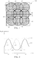
- FIG.1 illustrates a display device 100 operated in a normal mode.
- FIG.2 illustrates a light intensity diagram in the normal mode of FIG.1 .
- FIG.3 illustrates the display device 100 operated in a peak mode.
- FIG.4 illustrates a light intensity diagram in the peak mode of FIG.3 .
- a dimming zone d1 to a dimming zone d9 may be arranged and planned in coordinates defined by a horizontal axis X and a vertical axis Y.
- the dimming zone d2, the dimming zone d5 and the dimming zone d8 may be respectively corresponding to a zone z2, a zone z5 and a zone z8.
- Each dimming zone shown in FIG.1 and FIG.3 may be corresponding to one pixel or a plurality of pixels.
- the horizontal axis is corresponding to the horizontal X in FIG.1
- the vertical axis is corresponding to the light intensity.
- the display device 100 may be operated in the normal mode.
- the light emitted by the dimming zone d2 may be corresponding to a light intensity waveform w1 in the zone z2;
- the light emitted by the dimming zone d5 may be corresponding to a light intensity waveform w2 in the zone z5;
- the light emitted by the dimming zone d8 may be corresponding to a light intensity waveform w3 in the zone z8.
- the light emitted by the dimming zone d2, the dimming zone d5 and the dimming zone d8 may be corresponding to a light intensity waveform wn along the axis X.
- the light intensity waveform wn may be generated according to the light intensity waveform w1, the light intensity waveform w2 and the light intensity waveform w3.
- the light intensity waveform wn may be generated by summing up the light intensity waveform w1, the light intensity waveform w2 and the light intensity waveform w3 with consideration of the optical mechanical design and optical components.
- the light intensity expressed by the light intensity waveform wn at the junction x12 may not be excessively reduced by adding the light intensities expressed by the light intensity waveform w1 and the light intensity waveform w2.
- the light intensity expressed by the light intensity waveform wn may not be excessively reduced.
- the light intensity expressed by the light intensity waveform wn may be approximately kept the same.
- the display device 100 may be operated in the peak mode.
- the light emitted by the dimming zone d2, the dimming zone d5 and the dimming zone d8 may be corresponding to a light intensity waveform wd along the axis X.
- the light intensity waveform wd may be substantially determined by the light emitted by the dimming zone d5.
- the light intensity waveform wd may go down at the edges of the zone z5, and the brightness may be lower when approaching to the edges of the zone z5.
- an operation voltage of a driving transistor of the dimming zone d5 may be increased to increase the brightness of a light-emitting diode of the dimming zone d5.
- the light intensity waveform wd may be pulled up to form a light intensity waveform wp.
- the overall brightness may be increased, and the brightness at the edges of the dimming zone d5 may be increased.
- FIG.5 is a circuit diagram of a light-emitting device LD according to an embodiment.
- the light-emitting device LD may be disposed in at least one dimming zone of the dimming zone d1 to the dimming zone d9 to emit light.
- the light-emitting device LD may be a pixel element to display an image.
- the light-emitting device LD may be a backlight element to provide backlight for pixel element of a liquid crystal (LC) panel so as to display an image.
- LC liquid crystal
- embodiments of the disclosure are not limited thereto.
- the light-emitting device LD may include a light-emitting unit 510.
- the light-emitting unit 510 may include a driving transistor 511 and a light-emitting diode 512.
- the driving transistor 511 may include a first terminal 511s, a second terminal 511d and a first gate terminal 511g.
- the first terminal 511s may be used to receive an operation voltage Vdd.
- the light-emitting diode 512 may be coupled to the second terminal 511d and used to receive a driving current IDS.
- the operation voltage Vdd is variable according to an embodiment.
- the driving transistor 511 may be operated in a saturation region as described below.
- the light-emitting diode 512 may include an inorganic light-emitting diode, an organic light-emitting diode, a mini light-emitting diode (mini LED), a micro light-emitting diode (micro LED), a quantum dot light-emitting diode (QDLED or QLED), a fluorescence material, a phosphor material, other suitable materials or a combination of the abovementioned element and/or materials; however, embodiments are not limited thereto.
- mini LED mini light-emitting diode
- micro LED micro light-emitting diode
- QDLED or QLED quantum dot light-emitting diode
- fluorescence material a phosphor material, other suitable materials or a combination of the abovementioned element and/or materials; however, embodiments are not limited thereto.
- the first gate terminal 511g may be used to receive a data signal Sd from a data line Ldata.
- the conductivity of the driving transistor 511 may be controlled according to the data signal Sd.
- the driving current IDS when the driving transistor 511 has a higher conductivity, the driving current IDS may be larger, and the light intensity of the light-emitting diode 512 may be higher.
- the driving current IDS in the normal mode, the driving current IDS may have a current value In; and in the peak mode, the driving current IDS may have a current value Ip.
- the current value In may be smaller than the current value Ip (In ⁇ Ip).
- the current value Ip may be larger than two times the current value In, three times the current value In or four times the current value In, but embodiments are not limited thereto.
- the driving current IDS is larger, the light intensity of the light-emitting diode 512 may be higher.
- the operation voltage Vdd when the light-emitting diode 512 is operated to provide a first brightness B1, the operation voltage Vdd may be at a first voltage value V1.
- the operation voltage Vdd when the light-emitting diode 512 is operated to provide a second brightness B2, the operation voltage Vdd may be at a second voltage value V2.
- the second voltage value V2 may be lower than the first voltage value V1 (V2 ⁇ VI).
- the second brightness B2 may be lower than the first brightness B1 (B2 ⁇ B1).
- the light-emitting diode 512 in the normal mode (e.g., FIG.1 ), the light-emitting diode 512 may be operated to provide the second brightness B2.
- the light-emitting diode 512 may be operated to provide the first brightness B1.
- the second voltage value V2 may be between 1% to 100% of the first voltage value V1 (1% ⁇ V2/V1 ⁇ 100%).
- the second voltage value V2 may be 5%, 10%, 20%, 40%, 60% or 80% of the first voltage value VI, and embodiments are not limited thereto.
- the structure of FIG.5 is merely an example instead of limiting the structure of the light-emitting unit 510.
- the first terminal 511s and the second terminal 511d may respectively be a source terminal and a drain terminal of the driving transistor 511.
- the light-emitting diode 512 may include an anode coupled to the second terminal 511d and a cathode coupled to a reference voltage terminal to receive a reference voltage Vss.
- the light-emitting device may further include a capacitor Cst and a switch SW.
- the capacitor Cst may be coupled between the first terminal 511s and the first gate terminal 511g.
- the switch SW may be coupled between the data line Ldata and the first gate terminal 511g to control whether the data signal Sd is sent to the first gate terminal 511g.
- FIG.6 illustrates the voltages and currents outputted by the driving transistor 511 in FIG.5 .
- the horizontal axis of FIG.6 may be corresponding to a voltage difference between the first terminal 511s and the second terminal 511d.
- the vertical axis of FIG.6 may be corresponding to the driving current IDS of the driving transistor 511.
- a load line 611 may be a loading reference line of adjusting the voltage difference between the first terminal 511s and the second terminal 511d when the operation voltage Vdd is equal to the first voltage value V1.
- a curve Cp may be corresponding to the peak mode, and another curve Cn may be corresponding to the normal mode.
- FIG.5 there may be a voltage difference between the first gate terminal 511g and the first terminal 511s, and the voltage difference between the first gate terminal 511g and the first terminal 511s may be adjusted according to the data signal Sd.
- the curve Cp and the curve Cn may be corresponding to different voltage differences between the first gate terminal 511g and the first terminal 511s.
- the driving current IDS may have the current value Ip and the corresponding voltage difference between the first terminal 511s and the second terminal 511d may be at a voltage value VDSy; and under the normal mode, the driving current IDS may have the current value In and the corresponding voltage difference between the first terminal 511s and the second terminal 511d may be at a voltage value VDSz.
- the operation voltage Vdd may be adjusted from the first voltage value V1 to be at the second voltage value V2 under the normal mode, and the voltage difference between the first terminal 511s and the second terminal 511d may be adjusted from the voltage value VDSz to be at a voltage value VDSx.
- the voltage value VDSz may be larger than the voltage value VDSy (VDSz > VDSy), and the voltage value VDSy may be larger than the voltage value VDSx (VDSy > VDSx).
- the driving transistor 511 When the voltage difference between the first terminal 511s and the second terminal 511d is larger than a voltage value VDSsat, the driving transistor 511 may be operated in the saturation region Rsa. Hence, when the voltage difference between the first terminal 511s and the second terminal 511d is adjusted from the voltage value VDSz to the voltage value VDSx, the driving current IDS may be maintained to have the current value In. The light intensity of the light emitted by the light-emitting diode 512 in a normal mode may not be affected. In the normal mode, the operation voltage Vdd can be adjusted from the first voltage value V1 to the second voltage value V2 without affecting light intensity, reducing the power consumption to save power.
- FIG.7 illustrates a light-emitting device LD according to another embodiment.
- the light-emitting device LD may further include a light-emitting unit 710.
- the light-emitting unit 710 may include a driving transistor 711 and a light-emitting diode 712.
- the driving transistor 711 may include a third terminal 711s, a fourth terminal 711d and a second gate terminal 711g.
- the third terminal 711s may be used to receive an operation voltage Vdd2.
- the light-emitting diode 712 may be coupled to the fourth terminal 711d to receive a driving current IDS2.
- the operation voltage Vdd2 may be variable, and the operation voltage Vdd2 may be independent from the operation voltage Vdd. In other words, the operation voltage Vdd and the operation voltage Vdd2 may be set at two different voltage values. For example, when the light-emitting unit 510 is operated in the normal mode or the peak mode, the light-emitting unit 710 may be independently operated in the normal mode or the peak mode without being limited by the operation mode of the light-emitting unit 510.
- the light-emitting diode 712 may be coupled to the reference voltage terminal to receive the reference voltage Vss.
- a cathode of the light-emitting diode 712 may be coupled to the cathode of the light-emitting diode 512.
- the second gate terminal 711g may receive a data signal Sd2 from a data line Ldata2.
- the light-emitting unit 710 may further include a capacitor Cst2 and a switch SW2, but embodiments are not limited thereto.
- the structure and operation principles of the light-emitting unit 710 may be similar to that of the light-emitting diode 510, so it is not repeatedly described.
- FIG.7 may merely provide an example, and the light-emitting unit 710 may be not limited to the structure shown in FIG.7 .
- the light-emitting device LD it is merely an example for the light-emitting device LD to include two light-emitting units. According to another embodiment, more light-emitting units may be included.
- FIG. 8 illustrate a side view of display equipment 800 according to an embodiment.
- the display equipment may include the light-emitting device LD and a liquid crystal panel LC.
- the light-emitting device LD may be as shown in FIG.5 and FIG.7 , and its structure and operation principles are not repeatedly described.
- the liquid crystal panel LC may be disposed above the light-emitting device LD. According to the embodiment of FIG.8 , the light-emitting device LD may be used to provide backlight for the liquid crystal panel LC to display images.
- FIG.9 illustrates a system 900 according to an embodiment.
- the system 900 may include a voltage converter 910, a voltage converter 920, a controller 930 and a display unit 940.
- the voltage converter 910, the voltage converter 920 and the controller 930 may be respectively coupled to the display unit 940.
- the controller 930 may be coupled to the voltage converter 920.
- the display unit 940 may the foresaid light-emitting device LD or the display equipment 800 to provide backlight or display images.
- Each of the voltage converter 910 and the voltage converter 920 may include a DC (direct current) to DC converter, but embodiments are not limited thereto.
- the voltage converter 910 and the voltage converter 920 may respectively provide the foresaid the reference voltage Vss and the operation voltage Vdd to the display unit 940.
- the controller 930 may receive display content to provide the data signal to the display unit 940 according to the display content.
- the said data signal may include foresaid data signal Sd and the data signal Sd2.
- the controller 930 may control the voltage converter 920 according to the display content to adjust the operation voltage Vdd for the operation voltage Vdd to be at a lower voltage value in the normal mode and at a higher voltage value in the peak mode.
- the controller 930 may be (but not limited to) a timing controller.
- An algorithm used to control the operation voltage Vdd may be embedded to the control 930, but embodiments are not limited thereto.
- a screen of an in-vehicle computer may display a map and a speedometer.
- the condition may be like the normal mode shown in FIG.1 .
- the operation voltage Vdd and the operation voltage Vdd2 may be set lower, for example, to be at the second voltage value V2.
- the contrast may be higher.
- white numbers may be displayed on a black background.
- the condition may be like the peak mode shown in FIG.2 .
- the operation voltage Vdd and the operation voltage Vdd2 of the portion of displaying the speedometer may be set higher, for example, to be at the first voltage value V1.
- the abovementioned screen of an in-vehicle computer is merely an example, and embodiments are not limited thereto.
- a light-emitting device and display equipment may support operations under the normal mode and the peak mode, the display effect may not be affected, and the power consumption may be reduced.
Landscapes
- Engineering & Computer Science (AREA)
- Physics & Mathematics (AREA)
- Computer Hardware Design (AREA)
- General Physics & Mathematics (AREA)
- Theoretical Computer Science (AREA)
- Chemical & Material Sciences (AREA)
- Crystallography & Structural Chemistry (AREA)
- Control Of Indicators Other Than Cathode Ray Tubes (AREA)
Abstract
Description
- The disclosure relates to a light-emitting device and display equipment, and more particularly, a light-emitting device and display equipment related to a variable operation voltage.
- Electronic products have become indispensable necessities in modern society. With the rapid development of these electronic products, consumers have high expectations for the quality, function or price of these products.
- Although some electronic products can emit light or display images, they still have problems such as insufficient brightness or poor display quality.
- The present disclosure aims at providing a light-emitting device and display equipment related to a variable operation voltage for reducing the power consumption.
- This is achieved by a light-emitting device according to Claim 1 and display equipment according to Claim 11 here below. The dependent claims pertain to corresponding further developments and improvements.
- As will be seen more clearly from the detailed description following below, the light-emitting device includes a light-emitting unit. The light-emitting unit includes a driving transistor and a light-emitting diode. The driving transistor includes a first terminal, a second terminal and a first gate terminal where the first terminal is used to receive an operation voltage. The light-emitting diode is coupled to the second terminal and used to receive a driving current. The operation voltage is variable.
- As will be seen more clearly from the detailed description following below, the display equipment includes a light-emitting device and a liquid crystal panel. The light-emitting device includes a light-emitting unit including a driving transistor and a light-emitting diode. The driving transistor includes a first terminal, a second terminal and a first gate terminal where the first terminal is used to receive an operation voltage. The light-emitting diode is coupled to the second terminal and used to receive a driving current. The liquid crystal panel is disposed above the light-emitting device. The operation voltage is variable.
- In the following, the disclosure is further illustrated by way of example, taking reference to the accompanying drawings. Thereof
-
FIG. 1 illustrates a display device operated in a normal mode; -
FIG.2 illustrates a light intensity diagram in the normal mode ofFIG. 1 ; -
FIG.3 illustrates the display device operated in a peak mode; -
FIG.4 illustrates a light intensity diagram in the peak mode ofFIG.3 ; -
FIG. 5 is a circuit diagram of a light-emitting device according to an embodiment; -
FIG. 6 illustrates the voltages and currents of the driving transistor inFIG. 5 ; -
FIG.7 illustrates a light-emitting device according to another embodiment; -
FIG. 8 illustrate a side view of display equipment according to an embodiment; and -
FIG.9 illustrates a system according to an embodiment. - Here in the text, terms such as "about", "approximately" and "substantially" usually indicate that a difference between a real value and a described value is within a ratio of the described value; for example, the ratio may be within 20%. For example, the ratio may be 10%, 5%, 3%, 2% 1% or 0.5%. Here in the text, a described value may be an approximate value; that is, without mentioning terms such as "about", "approximately" and "substantially", a described value may still be an approximate value.
-
FIG.1 illustrates adisplay device 100 operated in a normal mode.FIG.2 illustrates a light intensity diagram in the normal mode ofFIG.1 .FIG.3 illustrates thedisplay device 100 operated in a peak mode.FIG.4 illustrates a light intensity diagram in the peak mode ofFIG.3 . - As shown in
FIG.1 andFIG.3 , in thedisplay device 100, a dimming zone d1 to a dimming zone d9 may be arranged and planned in coordinates defined by a horizontal axis X and a vertical axis Y. Along the horizontal axis X, the dimming zone d2, the dimming zone d5 and the dimming zone d8 may be respectively corresponding to a zone z2, a zone z5 and a zone z8. Each dimming zone shown inFIG.1 andFIG.3 may be corresponding to one pixel or a plurality of pixels. - In
FIG.2 andFIG.4 , the horizontal axis is corresponding to the horizontal X inFIG.1 , and the vertical axis is corresponding to the light intensity. - As shown in
FIG. 1 , when the dimming zone d1 to the dimming zone d9 are all emitting light, thedisplay device 100 may be operated in the normal mode. In the normal mode, the light emitted by the dimming zone d2 may be corresponding to a light intensity waveform w1 in the zone z2; the light emitted by the dimming zone d5 may be corresponding to a light intensity waveform w2 in the zone z5; and the light emitted by the dimming zone d8 may be corresponding to a light intensity waveform w3 in the zone z8. - As shown in
FIG. 1 and FIG.2 , the light emitted by the dimming zone d2, the dimming zone d5 and the dimming zone d8 may be corresponding to a light intensity waveform wn along the axis X. The light intensity waveform wn may be generated according to the light intensity waveform w1, the light intensity waveform w2 and the light intensity waveform w3. For example, the light intensity waveform wn may be generated by summing up the light intensity waveform w1, the light intensity waveform w2 and the light intensity waveform w3 with consideration of the optical mechanical design and optical components. As shown inFIG.2 , at a junction x12 of the zone z2 and the zone z5, although the light intensities expressed by the light intensity waveform w1 and the light intensity waveform w2 have respectively been reduced from maximum light intensities expressed by the two waveforms, the light intensity expressed by the light intensity waveform wn at the junction x12 may not be excessively reduced by adding the light intensities expressed by the light intensity waveform w1 and the light intensity waveform w2. Likewise, at a junction x23 of the zone z5 and the zone z8, the light intensity expressed by the light intensity waveform wn may not be excessively reduced. Hence, around the junction x23 of the zone z5 and the zone z8, the light intensity expressed by the light intensity waveform wn may be approximately kept the same. - As shown in
FIG.3 , when the dimming zone d5 is emitting light, but the dimming zone d1 to dimming d4 and the dimming zone d6 to the dimming zone d9 adjacent to the dimming zone d5 do not emit light, thedisplay device 100 may be operated in the peak mode. As shown inFIG.4 , in the peak mode, the light emitted by the dimming zone d2, the dimming zone d5 and the dimming zone d8 may be corresponding to a light intensity waveform wd along the axis X. The light intensity waveform wd may be substantially determined by the light emitted by the dimming zone d5. The light intensity waveform wd may go down at the edges of the zone z5, and the brightness may be lower when approaching to the edges of the zone z5. - In the condition of
FIG.3 , an operation voltage of a driving transistor of the dimming zone d5 may be increased to increase the brightness of a light-emitting diode of the dimming zone d5. In this way, the light intensity waveform wd may be pulled up to form a light intensity waveform wp. By enhancing the light intensity to be as expressed by the light intensity waveform wp, the overall brightness may be increased, and the brightness at the edges of the dimming zone d5 may be increased. - However, for performing the peak mode to increase the brightness at the edges of the dimming zone, the operation voltage received by the driving transistor of the dimming zone d5 has to be increased. If the operation voltage is kept at a level of the peak mode, the power consumption may remain high under the normal mode, causing excessive power consumption. Hence, according to embodiments, a variable operation voltage may be provided to reduce the excessive power consumption, and embodiments of the disclosure are not limited thereto.
FIG.5 is a circuit diagram of a light-emitting device LD according to an embodiment. The light-emitting device LD may be disposed in at least one dimming zone of the dimming zone d1 to the dimming zone d9 to emit light. The light-emitting device LD may be a pixel element to display an image. In another embodiment, the light-emitting device LD may be a backlight element to provide backlight for pixel element of a liquid crystal (LC) panel so as to display an image. However, embodiments of the disclosure are not limited thereto. - The light-emitting device LD may include a light-emitting
unit 510. The light-emittingunit 510 may include a drivingtransistor 511 and a light-emittingdiode 512. The drivingtransistor 511 may include afirst terminal 511s, asecond terminal 511d and afirst gate terminal 511g. Thefirst terminal 511s may be used to receive an operation voltage Vdd. The light-emittingdiode 512 may be coupled to thesecond terminal 511d and used to receive a driving current IDS. The operation voltage Vdd is variable according to an embodiment. The drivingtransistor 511 may be operated in a saturation region as described below. For example, the light-emittingdiode 512 may include an inorganic light-emitting diode, an organic light-emitting diode, a mini light-emitting diode (mini LED), a micro light-emitting diode (micro LED), a quantum dot light-emitting diode (QDLED or QLED), a fluorescence material, a phosphor material, other suitable materials or a combination of the abovementioned element and/or materials; however, embodiments are not limited thereto. - As shown in
FIG.5 , thefirst gate terminal 511g may be used to receive a data signal Sd from a data line Ldata. The conductivity of the drivingtransistor 511 may be controlled according to the data signal Sd. In an embodiment, when the drivingtransistor 511 has a higher conductivity, the driving current IDS may be larger, and the light intensity of the light-emittingdiode 512 may be higher. For example, in the normal mode, the driving current IDS may have a current value In; and in the peak mode, the driving current IDS may have a current value Ip. The current value In may be smaller than the current value Ip (In < Ip). For example, the current value Ip may be larger than two times the current value In, three times the current value In or four times the current value In, but embodiments are not limited thereto. When the driving current IDS is larger, the light intensity of the light-emittingdiode 512 may be higher. - As shown in
FIG.5 and FIG.6 , when the light-emittingdiode 512 is operated to provide a first brightness B1, the operation voltage Vdd may be at a first voltage value V1. When the light-emittingdiode 512 is operated to provide a second brightness B2, the operation voltage Vdd may be at a second voltage value V2. The second voltage value V2 may be lower than the first voltage value V1 (V2 < VI). The second brightness B2 may be lower than the first brightness B1 (B2 < B1). For example, in the normal mode (e.g.,FIG.1 ), the light-emittingdiode 512 may be operated to provide the second brightness B2. In the peak mode (e.g.,FIG.3 ), the light-emittingdiode 512 may be operated to provide the first brightness B1. The second voltage value V2 may be between 1% to 100% of the first voltage value V1 (1% < V2/V1 < 100%). For example, the second voltage value V2 may be 5%, 10%, 20%, 40%, 60% or 80% of the first voltage value VI, and embodiments are not limited thereto. - The structure of
FIG.5 is merely an example instead of limiting the structure of the light-emittingunit 510. For example, thefirst terminal 511s and thesecond terminal 511d may respectively be a source terminal and a drain terminal of the drivingtransistor 511. The light-emittingdiode 512 may include an anode coupled to thesecond terminal 511d and a cathode coupled to a reference voltage terminal to receive a reference voltage Vss. As shown inFIG.5 , the light-emitting device may further include a capacitor Cst and a switch SW. The capacitor Cst may be coupled between thefirst terminal 511s and thefirst gate terminal 511g. The switch SW may be coupled between the data line Ldata and thefirst gate terminal 511g to control whether the data signal Sd is sent to thefirst gate terminal 511g. -
FIG.6 illustrates the voltages and currents outputted by the drivingtransistor 511 inFIG.5 . As shown inFIG.5 and FIG.6 , the horizontal axis ofFIG.6 may be corresponding to a voltage difference between thefirst terminal 511s and thesecond terminal 511d. The vertical axis ofFIG.6 may be corresponding to the driving current IDS of the drivingtransistor 511. Aload line 611 may be a loading reference line of adjusting the voltage difference between thefirst terminal 511s and thesecond terminal 511d when the operation voltage Vdd is equal to the first voltage value V1. - In
FIG.6 , a curve Cp may be corresponding to the peak mode, and another curve Cn may be corresponding to the normal mode. TakingFIG.5 as an example, there may be a voltage difference between thefirst gate terminal 511g and thefirst terminal 511s, and the voltage difference between thefirst gate terminal 511g and thefirst terminal 511s may be adjusted according to the data signal Sd. The curve Cp and the curve Cn may be corresponding to different voltage differences between thefirst gate terminal 511g and thefirst terminal 511s. - According to the
load line 611, if the operation voltage Vdd is kept at the first voltage value VI, under the peak mode, the driving current IDS may have the current value Ip and the corresponding voltage difference between thefirst terminal 511s and thesecond terminal 511d may be at a voltage value VDSy; and under the normal mode, the driving current IDS may have the current value In and the corresponding voltage difference between thefirst terminal 511s and thesecond terminal 511d may be at a voltage value VDSz. According to an embodiment, as shown inFIG.6 , the operation voltage Vdd may be adjusted from the first voltage value V1 to be at the second voltage value V2 under the normal mode, and the voltage difference between thefirst terminal 511s and thesecond terminal 511d may be adjusted from the voltage value VDSz to be at a voltage value VDSx. For example, the voltage value VDSz may be larger than the voltage value VDSy (VDSz > VDSy), and the voltage value VDSy may be larger than the voltage value VDSx (VDSy > VDSx). - When the voltage difference between the
first terminal 511s and thesecond terminal 511d is larger than a voltage value VDSsat, the drivingtransistor 511 may be operated in the saturation region Rsa. Hence, when the voltage difference between thefirst terminal 511s and thesecond terminal 511d is adjusted from the voltage value VDSz to the voltage value VDSx, the driving current IDS may be maintained to have the current value In. The light intensity of the light emitted by the light-emittingdiode 512 in a normal mode may not be affected. In the normal mode, the operation voltage Vdd can be adjusted from the first voltage value V1 to the second voltage value V2 without affecting light intensity, reducing the power consumption to save power. -
FIG.7 illustrates a light-emitting device LD according to another embodiment. As shown inFIG.7 , the light-emitting device LD may further include a light-emittingunit 710. The light-emittingunit 710 may include a drivingtransistor 711 and a light-emittingdiode 712. The drivingtransistor 711 may include athird terminal 711s, afourth terminal 711d and asecond gate terminal 711g. Thethird terminal 711s may be used to receive an operation voltage Vdd2. Like the drivingtransistor 511, there may be a voltage difference between thethird terminal 711s and thefourth terminal 711d of the drivingtransistor 711, and another voltage difference between thethird terminal 711s and thesecond gate terminal 711g. The light-emittingdiode 712 may be coupled to thefourth terminal 711d to receive a driving current IDS2. The operation voltage Vdd2 may be variable, and the operation voltage Vdd2 may be independent from the operation voltage Vdd. In other words, the operation voltage Vdd and the operation voltage Vdd2 may be set at two different voltage values. For example, when the light-emittingunit 510 is operated in the normal mode or the peak mode, the light-emittingunit 710 may be independently operated in the normal mode or the peak mode without being limited by the operation mode of the light-emittingunit 510. - The light-emitting
diode 712 may be coupled to the reference voltage terminal to receive the reference voltage Vss. A cathode of the light-emittingdiode 712 may be coupled to the cathode of the light-emittingdiode 512. Thesecond gate terminal 711g may receive a data signal Sd2 from a data line Ldata2. The light-emittingunit 710 may further include a capacitor Cst2 and a switch SW2, but embodiments are not limited thereto. The structure and operation principles of the light-emittingunit 710 may be similar to that of the light-emittingdiode 510, so it is not repeatedly described.FIG.7 may merely provide an example, and the light-emittingunit 710 may be not limited to the structure shown inFIG.7 . InFIG.7 , it is merely an example for the light-emitting device LD to include two light-emitting units. According to another embodiment, more light-emitting units may be included. -
FIG. 8 illustrate a side view ofdisplay equipment 800 according to an embodiment. The display equipment may include the light-emitting device LD and a liquid crystal panel LC. The light-emitting device LD may be as shown inFIG.5 andFIG.7 , and its structure and operation principles are not repeatedly described. The liquid crystal panel LC may be disposed above the light-emitting device LD. According to the embodiment ofFIG.8 , the light-emitting device LD may be used to provide backlight for the liquid crystal panel LC to display images. -
FIG.9 illustrates asystem 900 according to an embodiment. Thesystem 900 may include avoltage converter 910, avoltage converter 920, acontroller 930 and adisplay unit 940. Thevoltage converter 910, thevoltage converter 920 and thecontroller 930 may be respectively coupled to thedisplay unit 940. Thecontroller 930 may be coupled to thevoltage converter 920. Thedisplay unit 940 may the foresaid light-emitting device LD or thedisplay equipment 800 to provide backlight or display images. Each of thevoltage converter 910 and thevoltage converter 920 may include a DC (direct current) to DC converter, but embodiments are not limited thereto. Thevoltage converter 910 and thevoltage converter 920 may respectively provide the foresaid the reference voltage Vss and the operation voltage Vdd to thedisplay unit 940. Thecontroller 930 may receive display content to provide the data signal to thedisplay unit 940 according to the display content. For example, the said data signal may include foresaid data signal Sd and the data signal Sd2. Thecontroller 930 may control thevoltage converter 920 according to the display content to adjust the operation voltage Vdd for the operation voltage Vdd to be at a lower voltage value in the normal mode and at a higher voltage value in the peak mode. Thecontroller 930 may be (but not limited to) a timing controller. An algorithm used to control the operation voltage Vdd may be embedded to thecontrol 930, but embodiments are not limited thereto. - For example, a screen of an in-vehicle computer (a.k.a. carputer) may display a map and a speedometer. In a portion of displaying the map, because displayed patterns may often fill the portion to the full, the condition may be like the normal mode shown in
FIG.1 . The operation voltage Vdd and the operation voltage Vdd2 may be set lower, for example, to be at the second voltage value V2. In another portion of displaying the speedometer, the contrast may be higher. For example, white numbers may be displayed on a black background. Hence, the condition may be like the peak mode shown inFIG.2 . The operation voltage Vdd and the operation voltage Vdd2 of the portion of displaying the speedometer may be set higher, for example, to be at the first voltage value V1. The abovementioned screen of an in-vehicle computer is merely an example, and embodiments are not limited thereto. - In summary, a light-emitting device and display equipment provided by embodiments may support operations under the normal mode and the peak mode, the display effect may not be affected, and the power consumption may be reduced.
Claims (15)
- A light-emitting device (LD) characterized by comprising:a first light-emitting unit (510), comprising:a first driving transistor (511) comprising a first terminal (511s), a second terminal (511d) and a first gate terminal (511g) wherein the first terminal (511s) is configured to receive a first operation voltage (Vdd); anda first light-emitting diode (512) coupled to the second terminal (511d) and configured to receive a first driving current (IDS);wherein the first operation voltage (Vdd) is variable.
- The light-emitting device (LD) of claim 1, wherein the first gate terminal (511s) is configured to receive a data signal (Sd) from a data line (Ldata), and the light-emitting device (LD) further comprises a switch (SW) coupled between the first gate terminal (511g) and the data line (Ldata).
- The light-emitting device (LD) of claim 1, wherein the first operation voltage (Vdd) is at a first voltage value (VI) when the first light-emitting diode (512) is operated to provide a first brightness (B1), the first operation voltage is at a second voltage value (V2) when the first light-emitting diode (512) is operated to provide a second brightness (B2), and the second voltage value (V2) is less than the first voltage value (VI).
- The light-emitting device (LD) of claim 1, wherein the first driving transistor (511) is operated in a saturation region (Rsa).
- The light-emitting device (LD) of claim 1, wherein the light-emitting device (LD) further comprises a capacitor (Cst) coupled between the first terminal (511s) and the first gate terminal (511g), and the first light-emitting diode (512) is further coupled to a reference voltage terminal and configured to receive a reference voltage (Vss).
- The light-emitting device (LD) of claim 1, further comprising:a second light-emitting unit (710), comprising:a second driving transistor (711) comprising a third terminal (711s), a fourth terminal (711d) and a second gate terminal (711g) wherein the third terminal (711s) is configured to receive a second operation voltage (Vdd2); anda second light-emitting diode (712) coupled to the fourth terminal (711d);wherein the second operation voltage (Vdd2) is variable, and the second operation voltage (Vdd2) is independent from the first operation voltage (Vdd).
- The light-emitting device (LD) of claim 6, wherein a cathode terminal of the first light-emitting diode (512) is coupled to a cathode terminal of the second light-emitting diode (712), and the light-emitting device (LD) further comprises a capacitor (Cst2) coupled between the third terminal (711s) and the second gate terminal (711g).
- Display equipment (800) characterized by comprising:a light-emitting device (LD), comprising:
a first light-emitting unit (510), comprising:a first driving transistor (511) comprising a first terminal (511s), a second terminal (511d) and a first gate terminal (511g) wherein the first terminal (511s) is configured to receive a first operation voltage (Vdd); anda first light-emitting diode (512) coupled to the second terminal (511d) and configured to receive a first driving current (IDS); anda liquid crystal panel (LC) disposed above the light-emitting device (LD);wherein the first operation voltage (Vdd) is variable. - The display equipment (800) of claim 8, wherein the first gate terminal (511g) is configured to receive a data signal (Sd) from a data line (Ldata), and the display equipment (800) further comprises a switch (SW) coupled between the first gate terminal (511g) and the data line (Ldata).
- The display equipment (800) of claim 8, wherein the first operation voltage (Vdd) is at a first voltage value (VI) when the first light-emitting diode (512) is operated to provide a first brightness (B1), the first operation voltage (Vdd) is at a second voltage value (V2) when the first light-emitting diode (512) is operated to provide a second brightness (B2), and the second voltage value (V2) is less than the first voltage value (VI).
- The display equipment (800) of claim 8, wherein the first driving transistor (511) is operated in a saturation region (Rsa).
- The display equipment (800) of claim 8, wherein the display equipment (800) further comprises a capacitor (Cst) coupled between the first terminal (511s) and the first gate terminal (511g), and the first light-emitting diode (512) is further coupled to a reference voltage terminal and configured to receive a reference voltage (Vss).
- The display equipment (800) of claim 8, further comprising:a second light-emitting unit (710), comprising:a second driving transistor (711) comprising a third terminal (711s), a fourth terminal (711d) and a second gate terminal (711g) wherein the third terminal (711s) is configured to receive a second operation voltage (Vdd2); anda second light-emitting diode (712) coupled to the fourth terminal (711d);wherein the second operation voltage (Vdd2) is variable, and the second operation voltage (Vdd2) is independent from the first operation voltage (Vdd).
- The display equipment (800) of claim 13, wherein a cathode terminal of the first light-emitting diode (512) is coupled to a cathode terminal of the second light-emitting diode (712).
- The display equipment (800) of claim 13, further comprising a capacitor (Cst2) coupled between the third terminal (711s) and the second gate terminal (711g).
Applications Claiming Priority (2)
| Application Number | Priority Date | Filing Date | Title |
|---|---|---|---|
| US201962844752P | 2019-05-08 | 2019-05-08 | |
| CN202010047807.6A CN111916030B (en) | 2019-05-08 | 2020-01-16 | Light-emitting devices and display equipment |
Publications (1)
| Publication Number | Publication Date |
|---|---|
| EP3736802A1 true EP3736802A1 (en) | 2020-11-11 |
Family
ID=70553988
Family Applications (1)
| Application Number | Title | Priority Date | Filing Date |
|---|---|---|---|
| EP20173148.6A Ceased EP3736802A1 (en) | 2019-05-08 | 2020-05-06 | Light-emitting device and display equipment related to variable operation voltage used for reducing power consumption |
Country Status (2)
| Country | Link |
|---|---|
| US (1) | US11151950B2 (en) |
| EP (1) | EP3736802A1 (en) |
Families Citing this family (1)
| Publication number | Priority date | Publication date | Assignee | Title |
|---|---|---|---|---|
| TW202533196A (en) * | 2024-02-01 | 2025-08-16 | 群創光電股份有限公司 | Display device |
Citations (3)
| Publication number | Priority date | Publication date | Assignee | Title |
|---|---|---|---|---|
| US20080170054A1 (en) * | 2006-05-25 | 2008-07-17 | Cehn-Jean Chou | Structure and drive scheme for light emitting device matrix as display light source |
| US20130082910A1 (en) * | 2011-09-29 | 2013-04-04 | Lg Display Co., Ltd. | Organic light emitting diode display device |
| US20140354624A1 (en) * | 2011-05-17 | 2014-12-04 | Ignis Innovation Inc. | Systems and methods for display systems with dynamic power control |
Family Cites Families (16)
| Publication number | Priority date | Publication date | Assignee | Title |
|---|---|---|---|---|
| TWI248319B (en) * | 2001-02-08 | 2006-01-21 | Semiconductor Energy Lab | Light emitting device and electronic equipment using the same |
| JP3986051B2 (en) * | 2002-04-30 | 2007-10-03 | 株式会社半導体エネルギー研究所 | Light emitting device, electronic equipment |
| US7079091B2 (en) * | 2003-01-14 | 2006-07-18 | Eastman Kodak Company | Compensating for aging in OLED devices |
| GB2430069A (en) * | 2005-09-12 | 2007-03-14 | Cambridge Display Tech Ltd | Active matrix display drive control systems |
| US7286123B2 (en) * | 2005-12-13 | 2007-10-23 | System General Corp. | LED driver circuit having temperature compensation |
| US20080024528A1 (en) * | 2006-07-28 | 2008-01-31 | Samsung Electro-Mechanics Co., Ltd. | Apparatus and method for adjusting color characteristics of display system using diffractive optical modulator |
| US8456492B2 (en) * | 2007-05-18 | 2013-06-04 | Sony Corporation | Display device, driving method and computer program for display device |
| JP2009053576A (en) * | 2007-08-29 | 2009-03-12 | Eastman Kodak Co | Active matrix type display device |
| JP5015714B2 (en) * | 2007-10-10 | 2012-08-29 | グローバル・オーエルイーディー・テクノロジー・リミテッド・ライアビリティ・カンパニー | Pixel circuit |
| JP5184042B2 (en) * | 2007-10-17 | 2013-04-17 | グローバル・オーエルイーディー・テクノロジー・リミテッド・ライアビリティ・カンパニー | Pixel circuit |
| KR101178910B1 (en) | 2009-07-30 | 2012-09-03 | 삼성디스플레이 주식회사 | Organic Light Emitting Display Device and Driving Voltage Setting Method Thereof |
| CN104658485B (en) | 2015-03-24 | 2017-03-29 | 京东方科技集团股份有限公司 | OLED driving compensation circuit and driving method thereof |
| CN105609047B (en) * | 2016-01-04 | 2018-05-18 | 京东方科技集团股份有限公司 | Pixel circuit and its driving method, display panel |
| KR102544322B1 (en) * | 2016-09-26 | 2023-06-19 | 삼성디스플레이 주식회사 | Light emitting display device |
| CN110364115B (en) * | 2018-04-11 | 2022-04-15 | 伊格尼斯创新公司 | Display system with controllable connection |
| US20200219435A1 (en) * | 2019-01-09 | 2020-07-09 | Mikro Mesa Technology Co., Ltd. | Light-emitting diode driving circuit, driving method, and display using the same |
-
2020
- 2020-04-13 US US16/847,575 patent/US11151950B2/en active Active
- 2020-05-06 EP EP20173148.6A patent/EP3736802A1/en not_active Ceased
Patent Citations (3)
| Publication number | Priority date | Publication date | Assignee | Title |
|---|---|---|---|---|
| US20080170054A1 (en) * | 2006-05-25 | 2008-07-17 | Cehn-Jean Chou | Structure and drive scheme for light emitting device matrix as display light source |
| US20140354624A1 (en) * | 2011-05-17 | 2014-12-04 | Ignis Innovation Inc. | Systems and methods for display systems with dynamic power control |
| US20130082910A1 (en) * | 2011-09-29 | 2013-04-04 | Lg Display Co., Ltd. | Organic light emitting diode display device |
Also Published As
| Publication number | Publication date |
|---|---|
| US11151950B2 (en) | 2021-10-19 |
| US20200357347A1 (en) | 2020-11-12 |
Similar Documents
| Publication | Publication Date | Title |
|---|---|---|
| KR101381350B1 (en) | Backlight unit and liquid crystal display device withthe same and dimming method thereof | |
| TWI415097B (en) | Liquid crystal display device and driving method thereof | |
| KR20130132702A (en) | Selective dimming to reduce power of a light emitting display device | |
| JP2025541899A (en) | Display driving architecture, display driving method, and display device | |
| KR20090118225A (en) | Display device and driving method thereof | |
| KR20170045452A (en) | Backlight unit, method for driving thereof, and display device including the same | |
| KR100618574B1 (en) | Driving circuit of organic electroluminescent element | |
| KR102875983B1 (en) | Display device | |
| KR20110138722A (en) | OLED display and power supply for same | |
| KR20170059541A (en) | Backlight unit and display apparatus including the same | |
| KR101046114B1 (en) | Low Power Driven LED Display Board | |
| CN112017596A (en) | Display panel, brightness adjusting method and display device | |
| KR20080073950A (en) | Backlight unit and liquid crystal display including the same | |
| CN102446496A (en) | Backlight device, display device including the backlight device, and lighting device | |
| US11151950B2 (en) | Light-emitting device and display equipment related to variable operation voltage used for reducing power consumption | |
| KR101968911B1 (en) | organic light-emitting dIODE DISPLAY DEVICE AND DRIVING METHOD THEREOF | |
| US20150371593A1 (en) | Color Dependent Content Adaptive Backlight Control | |
| KR101423518B1 (en) | Liquid crystal display device | |
| CN114203092A (en) | Display panel and driving method of display panel | |
| KR20160078618A (en) | Organic light emitting display device | |
| US11289008B2 (en) | Pixel circuit | |
| KR101886428B1 (en) | Organic light emmitting display device and driving method thereof | |
| CN111916030B (en) | Light-emitting devices and display equipment | |
| KR20120061542A (en) | Light emitting diode backlight and liquid crystal display device including the same | |
| KR102490380B1 (en) | Liquid crystal display |
Legal Events
| Date | Code | Title | Description |
|---|---|---|---|
| PUAI | Public reference made under article 153(3) epc to a published international application that has entered the european phase |
Free format text: ORIGINAL CODE: 0009012 |
|
| STAA | Information on the status of an ep patent application or granted ep patent |
Free format text: STATUS: THE APPLICATION HAS BEEN PUBLISHED |
|
| AK | Designated contracting states |
Kind code of ref document: A1 Designated state(s): AL AT BE BG CH CY CZ DE DK EE ES FI FR GB GR HR HU IE IS IT LI LT LU LV MC MK MT NL NO PL PT RO RS SE SI SK SM TR |
|
| AX | Request for extension of the european patent |
Extension state: BA ME |
|
| STAA | Information on the status of an ep patent application or granted ep patent |
Free format text: STATUS: REQUEST FOR EXAMINATION WAS MADE |
|
| 17P | Request for examination filed |
Effective date: 20210511 |
|
| RBV | Designated contracting states (corrected) |
Designated state(s): AL AT BE BG CH CY CZ DE DK EE ES FI FR GB GR HR HU IE IS IT LI LT LU LV MC MK MT NL NO PL PT RO RS SE SI SK SM TR |
|
| STAA | Information on the status of an ep patent application or granted ep patent |
Free format text: STATUS: EXAMINATION IS IN PROGRESS |
|
| 17Q | First examination report despatched |
Effective date: 20220218 |
|
| STAA | Information on the status of an ep patent application or granted ep patent |
Free format text: STATUS: THE APPLICATION HAS BEEN REFUSED |
|
| 18R | Application refused |
Effective date: 20241018 |