EP3736738A1 - Ic tag - Google Patents
Ic tag Download PDFInfo
- Publication number
- EP3736738A1 EP3736738A1 EP18898329.0A EP18898329A EP3736738A1 EP 3736738 A1 EP3736738 A1 EP 3736738A1 EP 18898329 A EP18898329 A EP 18898329A EP 3736738 A1 EP3736738 A1 EP 3736738A1
- Authority
- EP
- European Patent Office
- Prior art keywords
- dipole antenna
- chip
- tag
- antenna
- substrate
- Prior art date
- Legal status (The legal status is an assumption and is not a legal conclusion. Google has not performed a legal analysis and makes no representation as to the accuracy of the status listed.)
- Granted
Links
Images


Classifications
-
- G—PHYSICS
- G06—COMPUTING OR CALCULATING; COUNTING
- G06K—GRAPHICAL DATA READING; PRESENTATION OF DATA; RECORD CARRIERS; HANDLING RECORD CARRIERS
- G06K19/00—Record carriers for use with machines and with at least a part designed to carry digital markings
- G06K19/06—Record carriers for use with machines and with at least a part designed to carry digital markings characterised by the kind of the digital marking, e.g. shape, nature, code
- G06K19/067—Record carriers with conductive marks, printed circuits or semiconductor circuit elements, e.g. credit or identity cards also with resonating or responding marks without active components
- G06K19/07—Record carriers with conductive marks, printed circuits or semiconductor circuit elements, e.g. credit or identity cards also with resonating or responding marks without active components with integrated circuit chips
- G06K19/077—Constructional details, e.g. mounting of circuits in the carrier
-
- G—PHYSICS
- G06—COMPUTING OR CALCULATING; COUNTING
- G06K—GRAPHICAL DATA READING; PRESENTATION OF DATA; RECORD CARRIERS; HANDLING RECORD CARRIERS
- G06K19/00—Record carriers for use with machines and with at least a part designed to carry digital markings
- G06K19/06—Record carriers for use with machines and with at least a part designed to carry digital markings characterised by the kind of the digital marking, e.g. shape, nature, code
- G06K19/067—Record carriers with conductive marks, printed circuits or semiconductor circuit elements, e.g. credit or identity cards also with resonating or responding marks without active components
- G06K19/07—Record carriers with conductive marks, printed circuits or semiconductor circuit elements, e.g. credit or identity cards also with resonating or responding marks without active components with integrated circuit chips
- G06K19/077—Constructional details, e.g. mounting of circuits in the carrier
- G06K19/07749—Constructional details, e.g. mounting of circuits in the carrier the record carrier being capable of non-contact communication, e.g. constructional details of the antenna of a non-contact smart card
- G06K19/07773—Antenna details
- G06K19/07786—Antenna details the antenna being of the HF type, such as a dipole
-
- B—PERFORMING OPERATIONS; TRANSPORTING
- B42—BOOKBINDING; ALBUMS; FILES; SPECIAL PRINTED MATTER
- B42D—BOOKS; BOOK COVERS; LOOSE LEAVES; PRINTED MATTER CHARACTERISED BY IDENTIFICATION OR SECURITY FEATURES; PRINTED MATTER OF SPECIAL FORMAT OR STYLE NOT OTHERWISE PROVIDED FOR; DEVICES FOR USE THEREWITH AND NOT OTHERWISE PROVIDED FOR; MOVABLE-STRIP WRITING OR READING APPARATUS
- B42D25/00—Information-bearing cards or sheet-like structures characterised by identification or security features; Manufacture thereof
- B42D25/30—Identification or security features, e.g. for preventing forgery
- B42D25/305—Associated digital information
-
- G—PHYSICS
- G06—COMPUTING OR CALCULATING; COUNTING
- G06K—GRAPHICAL DATA READING; PRESENTATION OF DATA; RECORD CARRIERS; HANDLING RECORD CARRIERS
- G06K19/00—Record carriers for use with machines and with at least a part designed to carry digital markings
- G06K19/02—Record carriers for use with machines and with at least a part designed to carry digital markings characterised by the selection of materials, e.g. to avoid wear during transport through the machine
-
- H—ELECTRICITY
- H01—ELECTRIC ELEMENTS
- H01Q—ANTENNAS, i.e. RADIO AERIALS
- H01Q1/00—Details of, or arrangements associated with, antennas
- H01Q1/12—Supports; Mounting means
- H01Q1/22—Supports; Mounting means by structural association with other equipment or articles
- H01Q1/2208—Supports; Mounting means by structural association with other equipment or articles associated with components used in interrogation type services, i.e. in systems for information exchange between an interrogator/reader and a tag/transponder, e.g. in Radio Frequency Identification [RFID] systems
- H01Q1/2225—Supports; Mounting means by structural association with other equipment or articles associated with components used in interrogation type services, i.e. in systems for information exchange between an interrogator/reader and a tag/transponder, e.g. in Radio Frequency Identification [RFID] systems used in active tags, i.e. provided with its own power source or in passive tags, i.e. deriving power from RF signal
-
- H—ELECTRICITY
- H01—ELECTRIC ELEMENTS
- H01Q—ANTENNAS, i.e. RADIO AERIALS
- H01Q1/00—Details of, or arrangements associated with, antennas
- H01Q1/36—Structural form of radiating elements, e.g. cone, spiral, umbrella; Particular materials used therewith
- H01Q1/38—Structural form of radiating elements, e.g. cone, spiral, umbrella; Particular materials used therewith formed by a conductive layer on an insulating support
-
- H—ELECTRICITY
- H01—ELECTRIC ELEMENTS
- H01Q—ANTENNAS, i.e. RADIO AERIALS
- H01Q1/00—Details of, or arrangements associated with, antennas
- H01Q1/40—Radiating elements coated with or embedded in protective material
-
- H—ELECTRICITY
- H01—ELECTRIC ELEMENTS
- H01Q—ANTENNAS, i.e. RADIO AERIALS
- H01Q9/00—Electrically-short antennas having dimensions not more than twice the operating wavelength and consisting of conductive active radiating elements
- H01Q9/04—Resonant antennas
- H01Q9/16—Resonant antennas with feed intermediate between the extremities of the antenna, e.g. centre-fed dipole
- H01Q9/20—Two collinear substantially straight active elements; Substantially straight single active elements
- H01Q9/24—Shunt feed arrangements to single active elements, e.g. for delta matching
-
- H—ELECTRICITY
- H01—ELECTRIC ELEMENTS
- H01Q—ANTENNAS, i.e. RADIO AERIALS
- H01Q9/00—Electrically-short antennas having dimensions not more than twice the operating wavelength and consisting of conductive active radiating elements
- H01Q9/04—Resonant antennas
- H01Q9/16—Resonant antennas with feed intermediate between the extremities of the antenna, e.g. centre-fed dipole
- H01Q9/26—Resonant antennas with feed intermediate between the extremities of the antenna, e.g. centre-fed dipole with folded element or elements, the folded parts being spaced apart a small fraction of operating wavelength
- H01Q9/27—Spiral antennas
Definitions
- an inlet In recent years, a type of IC tag called an "inlet" has been proposed, in which an antenna pattern for radio frequency communication and an IC chip are mounted on a base sheet made of plastic or paper. Such inlets are used for the management of articles in a state of being sealed with resin and then attached to or embedded in the articles.
- the IC tag according to the present invention is an IC tag including: an IC chip; a dipole antenna for electrically transmitting and receiving information stored in the IC chip; and a sheet-shaped substrate that supports the IC chip and the dipole antenna, wherein 0.1 ⁇ R/L ⁇ 2.5 is satisfied, where R is a resistance value between two ends of the dipole antenna and L is a length of a path that connects the two ends of the dipole antenna while extending along the dipole antenna without passing through the IC chip.
Landscapes
- Engineering & Computer Science (AREA)
- Physics & Mathematics (AREA)
- General Physics & Mathematics (AREA)
- Theoretical Computer Science (AREA)
- Computer Hardware Design (AREA)
- Microelectronics & Electronic Packaging (AREA)
- Computer Networks & Wireless Communication (AREA)
- Details Of Aerials (AREA)
- Support Of Aerials (AREA)
- Credit Cards Or The Like (AREA)
Abstract
Description
- The present invention relates to an IC tag.
- In recent years, a type of IC tag called an "inlet" has been proposed, in which an antenna pattern for radio frequency communication and an IC chip are mounted on a base sheet made of plastic or paper. Such inlets are used for the management of articles in a state of being sealed with resin and then attached to or embedded in the articles.
- The above-described IC tags may be attached to linen articles for management of the linen articles, but it is common practice to use a metal detector to inspect the linen articles for the presence of metal contaminants at the time of shipment. However, the IC tags have an antenna pattern formed of metal, and thus, when a metal detector is used to inspect the linen articles having the IC tags attached thereto, the metal detector detects the IC tags as metal even if no metal contaminants are present in the linen articles. This poses a problem in that the inspection for actual metal contaminants cannot be performed smoothly.
- To address this problem,
Patent Literature 1 discloses an IC tag in which the resistance value of an antenna is set to 50 to 1000 Ω, and also discloses that the IC tag with an antenna resistance value in such a range does not respond to a metal detector. - Patent Literature 1:
JP 2016-33748A - However, even the IC tag of
Patent Literature 1 may be detected by a metal detector, and further improvement thus has been demanded. The present invention is intended to solve the above-described problem, and it is an object of the present invention to provide an IC tag that can be more reliably prevented from being detected by a metal detector. - The IC tag according to the present invention is an IC tag including: an IC chip; a dipole antenna for electrically transmitting and receiving information stored in the IC chip; and a sheet-shaped substrate that supports the IC chip and the dipole antenna, wherein 0.1 ≤ R/L ≤ 2.5 is satisfied, where R is a resistance value between two ends of the dipole antenna and L is a length of a path that connects the two ends of the dipole antenna while extending along the dipole antenna without passing through the IC chip.
- In the above-described IC tag, the length L may be not less than 120 mm and not more than 200 mm.
- In the above-described IC tag, the material of the dipole antenna may contain any one of silver, aluminum, and copper.
- The above-described IC tag may further include: a sheet-shaped cover that covers the IC chip and the antenna, the IC chip and the antenna being disposed between the cover and the substrate; and a pressure-sensitive adhesive that bonds the cover and the substrate.
- According to the present invention, it is possible to more reliably prevent an IC tag from being detected by a metal detector.
-
-
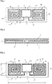
FIG. 1 is a plan view showing an embodiment of an IC tag according to the present invention; -
FIG. 2 is a cross-sectional view of the IC tag shown inFIG. 1 ; -
FIG. 3 is a plan view for illustrating an antenna of the IC tag shown inFIG. 1 ; -
FIG. 4 is a plan view showing the shape of a dipole antenna used in Example 1 and Comparative Example 1; -
FIG. 5 is a plan view showing the shape of a dipole antenna used in Example 2; -
FIG. 6 is a plan view showing the shape of a dipole antenna used in Example 3 and Comparative Example 2; -
FIG. 7 is a plan view showing the shape of a dipole antenna used in Example 4; and -
FIG. 8 is a plan view showing the shape of a dipole antenna used in Example 5. - An embodiment of an IC tag according to the present invention will be described below with reference to the drawings.
FIG. 1 is a plan view of the IC tag according to the present embodiment, andFIG. 2 is a cross-sectional view ofFIG. 1. FIG. 1 does not show a cover for the sake of convenience of illustration. As shown inFIGS. 1 and 2 , the IC tag according to the present embodiment includes a sheet-shaped substrate 1 formed in a rectangular shape, anIC chip 2 and adipole antenna 3 disposed on thissubstrate 1, and a sheet-shaped cover 4 that is formed in a rectangular shape and covers theIC chip 2 and thedipole antenna 3. Thesubstrate 1 and thecover 4 are bonded together using a pressure-sensitive adhesive 5. Each of these members will be described in detail below. - The
substrate 1 and thecover 4 are formed in the same shape, and the pressure-sensitive adhesive 5 is disposed so as to completely fill the gap between thesubstrate 1 and thecover 4. That is, the pressure-sensitive adhesive 5 covers theIC chip 2 and thedipole antenna 3 in such a manner that theIC chip 2 and thedipole antenna 3 are not exposed from the gap between thesubstrate 1 and thecover 4. - The materials of the
substrate 1 and thecover 4 are not particularly limited, and, for example, may be formed using polyethylene, polypropylene, polyethylene terephthalate, polyvinyl chloride, or the like. The thicknesses of thesubstrate 1 and thecover 4 are, for example, preferably 25 to 200 µm and more preferably 25 to 100 µm. - Hereinafter, as shown in
FIG. 1 , sides of thesubstrate 1 and thecover 4 in the lengthwise direction are referred to as afirst side 101 and asecond side 102, and sides of the same in the widthwise direction are referred to as athird side 103 and afourth side 104, for the sake of convenience of explanation. Accordingly, these sides are connected to each other in the order of thefirst side 101, thethird side 103, thesecond side 102, and thefourth side 104. - The
IC chip 2 is a known IC chip having a memory function, and is electrically connected to thedipole antenna 3 formed of a conductor. - In the present embodiment, a dipole antenna as shown in
FIG. 1 is used as an illustrative example. Specifically, thisdipole antenna 3 includes animpedance matching portion 31 disposed in the vicinity of the center of thesubstrate 1 in the lengthwise direction, and a pair ofdipole portions 32 extending from theimpedance matching portion 31 in the lengthwise direction of thesubstrate 1. Theimpedance matching portion 31 is formed in the shape of a rectangular frame having first to fourth sides. More specifically, afirst side 311 of theimpedance matching portion 31 is disposed somewhat spaced apart from thefirst side 101 of thesubstrate 1, and asecond side 312 is disposed along thesecond side 102 of thesubstrate 1. That is, in theimpedance matching portion 31, thefirst side 311, athird side 313, thesecond side 312, and afourth side 314 are connected to each other in this order. TheIC chip 2 is disposed in the vicinity of the center of thefirst side 311 of theimpedance matching portion 31. - Since the
dipole portions 32 have shapes symmetrical to each other, only one of them will be described. Thedipole portion 32 extends from thefirst side 311 of theimpedance matching portion 31 toward thefirst side 101 of thesubstrate 1, then extends along thefirst side 101, thethird side 103, and thesecond side 102 of thesubstrate 1, and further extends along thethird side 313 of theimpedance matching portion 31, thereby forming a rectangular frame. Thereafter, thedipole portion 32 extends spirally inside the frame. - The material of the
dipole antenna 3 is not particularly limited, and thedipole antenna 3 can be made of, for example, silver, copper, or aluminum. When silver is used, thedipole antenna 3 can be formed by applying a silver paste containing silver onto thesubstrate 1 through screen printing. On the other hand, when copper or aluminum is used, thedipole antenna 3 can be formed through etching. TheIC chip 2 can be fixed to theantenna 3 using, for example, a known flip-chip mounting procedure for electronic components. - The above-described
dipole antenna 3 enables transmission and reception of information stored in theIC chip 2 using, for example, radio waves in the UHF band. - The pressure-
sensitive adhesive 5 may be, for example, a rubber-based pressure-sensitive adhesive containing natural rubber or synthetic rubber as a main component. The thickness of the rubber-based pressure-sensitive adhesive 5 is not particularly limited, and is preferably 28 to 500 µm and more preferably 28 to 72 µm. Examples of the synthetic rubber to be used in the rubber-based pressure-sensitive adhesive 5 include, but not particularly limited to, styrene-isoprene-styrene block copolymers, styrene-butadiene-styrene block copolymers, hydrogenated products of the above-described styrene-based block copolymers, styrene-butadiene rubber (SBR), polyisoprene rubber (IR), polyisobutylene (PIB), and butyl rubber (IIR). - The rubber-based pressure-
sensitive adhesive 5 may further contain a tackifier, in addition to the above-described natural rubber or synthetic rubber. Examples of the tackifier include terpene phenol resins, rosin resins, and petroleum resins. The amount of resin to be used as the tackifier can be selected as appropriate within a range where the pressure-sensitive adhesion performance is not impaired. In addition to the above-described components, the rubber-based pressure-sensitive adhesive may optionally contain additives such as a softener, a plasticizer, a filler, an anti-aging agent, and a coloring agent as necessary. - As the pressure-
sensitive adhesive 5, not only the rubber-based pressure-sensitive adhesive but also an acrylic pressure-sensitive adhesive or a silicone pressure-sensitive adhesive can be used. - The
dipole antenna 3 according to the present embodiment has the following physical and electrical properties. The physical and electrical properties will be described with reference toFIG. 3 . First, as shown inFIG. 3 , the resistance value between two ends S1 and S2 of thedipole antenna 3 is defined as R (Ω), and the length of a path that connects the two ends S1 and S2 of thedipole antenna 3 while extending along thedipole antenna 3 without passing through the IC chip 2 (hereinafter, this path is referred to as "antenna path": indicated with the broken line inFIG. 3 ) is defined as L (cm). Thedipole antenna 3 according to the present embodiment satisfies the following formula (1). The antenna path passes through the center of the line width of thedipole antenna 1.
- This defines the resistance per unit length of the antenna path. When R/L is 0.1 or more, it becomes difficult for a current to flow, whereby the IC tag is prevented from being detected by a metal detector. On the other hand, when R/L is greater than 2.5, the communication range is reduced, whereby application software to which the IC tag is applicable may be limited. Accordingly, R/L is preferably 2.5 or less. In order to more reliably prevent the IC tag from being detected by a metal detector, it is more preferable that R/L satisfies the following formula (2) .

- The resistance value R (Ω) between the two ends S1 and S2 of the
antenna 3 is not particularly limited, and is, for example, preferably 10 to 50 Ω and more preferably 20 to 44 Ω. This is because, when the resistance value R is 10 Ω or more, it becomes difficult for a current to flow, and when the resistance value R is 50 Ω or less, the communication range is broad enough to stabilize communication. - Also, the length L of the above-described antenna path is not particularly limited, and is, for example, preferably 120 to 200 mm and more preferably 130 to 180 mm. This is because, when the length L of the antenna path is short, the communication becomes unstable, and when the antenna path is too long, the IC tag is more likely to be detected by a metal detector.
- The size of the outer shape of the
dipole antenna 3 is not particularly limited. In order to prevent the IC tag from being detected by a metal detector, the length X of the outer shape of thedipole antenna 3 in the lengthwise direction is, for example, preferably 60 mm or less and more preferably 40 mm or less. The length Y of the outer shape of thedipole antenna 3 in the widthwise direction is preferably 20 mm or less and more preferably 10 mm or less. Accordingly, the area (X × Y) of the outer shape of the dipole antenna is preferably 1200 mm2 and more preferably 400 mm2 or less. - The thickness of the
dipole antenna 3 is not particularly limited, and is, for example, preferably 20 µm or less, more preferably 15 µm or less, and particularly preferably 10 µm or less. For example, when thedipole antenna 3 is formed through printing the above-described silver paste, the thickness of thedipole antenna 3 can be adjusted more easily as compared with the case where thedipole antenna 3 is formed using copper or aluminum through etching, and the thickness of thedipole antenna 3 can be set to 10 µm or less. Accordingly, the IC tag can be more reliably prevented from being detected by a metal detector. - A metal detector by which the IC tag according to the present embodiment should not be detected may be, for example, a metal detector for detecting nonferrous metals. This is because, as described above, there are cases where the dipole antenna is formed of a nonferrous metal such as silver, copper, or aluminum. The detection sensitivity is preferably such that the IC tag is not detected when, for example, MUK-500 manufactured by NIKKA DENSOK LIMITED is used as a metal detector. This device has a detection sensitivity capable of detecting, as the smallest substance it can detect, a ball made of SUS having an outer diameter of 1.5 mm or more. Therefore, as an example of the metal detector by which the IC tag according to the present embodiment is not detected, a metal detector having the above-described detection sensitivity for nonferrous metals can be defined. It is to be noted, however, that such a metal detector is merely an illustrative example, and the present invention may be embodied based on the assumption that the metal detector is a metal detector for detecting iron.
- As described above, the IC tag according to the present embodiment in which the
dipole antenna 3 is configured to satisfy the above formula (1) can be prevented from being detected by a metal detector. - Although one embodiment of the present invention has been described above, the present invention is not limited to the above embodiment, and various changes can be made thereto without departing from the gist of the invention. Moreover, a plurality of modifications to be described below can be combined as appropriate.
- The shape of the above-described
dipole antenna 3 is merely an illustrative example, and various shapes can be adopted as long as the above formula (1) is satisfied. Moreover, the shape of the IC tag, i.e., the shapes of thesubstrate 1 and thecover 4 are also not particularly limited. In addition to an elongated shape such as described above, the IC tag may have various shapes including a rectangular shape, a circular shape, and a polygonal shape according to its use. Further, thesubstrate 1 and thecover 4 need not have the same shape. - In the above embodiment, the pressure-
sensitive adhesive 5 is applied so as to completely fill the gap between thesubstrate 1 and thecover 4. However, the present invention is not limited thereto. For example, the rubber-based pressure-sensitive adhesive 5 may be applied only to a peripheral edge portion of thesubstrate 1 and thecover 4 such that theIC chip 2 and theantenna 3 are surrounded by the pressure-sensitive adhesive 5. Thecover 4 and the pressure-sensitive adhesive 5 are not essential and may be omitted. - Examples of the present invention will be described below. However, the present invention is not limited to the following examples.
- IC tags according to Examples 1 to 5 and Comparative Examples 1 and 2 were prepared as follows. The IC tags of these examples and comparative examples used the same substrate and IC chip, but dipole antennas used therein were different from each other. Antennas of five types of shapes as shown in
FIGS. 4 to 8 were prepared, and antennas of three types of materials were prepared. InFIGS. 4 to 8 , the dotted line indicates the path L, and the numerical values indicate the lengths X and Y of the outer shape. As the substrate and a cover of each IC tag, polyethylene terephthalate films having a thickness of 50 µm were prepared. The dipole antenna was disposed between the substrate and the cover, and fixed using the above-described rubber-based pressure-sensitive adhesive. Then, the IC tags according to Examples 1 to 5 and Comparative Examples 1 and 2 were prepared as shown in Table 1 below. As described below, the antennas of the examples and the comparative examples were each made of a nonferrous metal.[Table 1] Shape of antenna Material of antenna Thickness Minimum width Path Length L Length X(1) Length Y(2) Area Volume resistivity Resistance R at two ends R/L (mm) (mm) (cm) (mm) (mm) (mm2) (Ω·m) (Ω) Ex. 1 FIG. 4 Silver paste 0.005 0.5 17.0 25 7.5 188 5.31 × 10⁻⁷ 36.1 2.12 Ex. 2 FIG. 5 Silver paste 0.005 0.5 17.4 30 7.5 255 5.95 × 10⁻⁷ 41.4 2.38 Ex. 3 FIG. 6 Silver paste 0.005 0.55 13.7 39 7.5 293 4.46 × 10⁻⁷ 22.2 1.62 Ex. 4 FIG. 7 Silver paste 0.015 0.72 14.1 53 4 212 1.53 × 10⁻⁷ 2 0.14 Ex. 5 FIG. 8 Silver paste 0.015 0.72 12.8 55 6 330 1.53 × 10⁻⁷ 1.8 0.14 Comp. Ex. 1 FIG. 4 Aluminum 0.01 0.5 17.0 25 7.5 188 2.65 × 10⁻⁸ 0.9 0.05 Comp. Ex. 2 FIG. 6 Copper 0.018 0.55 13.7 39 7.5 293 1.73 × 10⁻⁸ 0.24 0.018 (1) Length X in lengthwise direction
(2) Length Y in widthwise direction - Using MUK-500 manufactured by NIKKA DENSOK LIMITED as a metal detector, whether the metal detector could detect the IC tags according to the above-described examples and comparative example was examined. The detection levels in this device are 0 to 12. Specifically, the detection levels are as follows. That is, when balls made of SUS304 are used, this device cannot detect a ball with a diameter of 1 mm but can detect a ball with a diameter of 2 mm or more. The detection level when the device detects a ball with a diameter of 2 mm is 8, and the detection level when the device detects a ball with a diameter of 3 mm is 12. On the other hand, a detection level of 0 means that this metal detector cannot detect a target substance at all. That is, the closer the detection level is to 0, the more difficult it becomes for the metal detector to detect a target substance.
[Table 2] Detection Level Example 1 0 Example 2 0 Example 3 0 Example 4 3 Example 5 3 Comparative Example 1 12 Comparative Example 2 12 - In Examples 1 to 3, the R/L values were 1.5 or more, and the detection levels were all 0. That is, the IC tags of Examples 1 to 3 were not detected by the metal detector at all. In Examples 4 and 5, the R/L values were 1 or less and lower than those in Examples 1 to 3, but were not less than 0.1. The levels of detection by the metal detector were 3. That is, although the IC tags of Examples 4 and 5 were slightly detectable, they were acceptable depending on the intended use thereof. On the other hand, in Comparative Examples 1 and 2, the R/L values were both lower than 0.1, and the detection levels were 12. That is, the IC tags of Comparative Examples 1 and 2 were at the detection level of certain detection by the metal detector. Thus, the evaluation based on the R/L values showed that the IC tags of Examples 1 to 5 are all superior to the IC tags of Comparative Examples 1 and 2.
-
- 1
- Substrate
- 2
- IC chip
- 3
- Dipole antenna
- 4
- Cover
- 5
- Pressure-sensitive adhesive
Claims (4)
- An IC tag comprising:an IC chip;a dipole antenna for electrically transmitting and receiving information stored in the IC chip; anda sheet-shaped substrate that supports the IC chip and the dipole antenna,wherein 0.1 ≤ R/L ≤ 2.5 is satisfied, where R is a resistance value between two ends of the dipole antenna and L is a length of a path that connects the two ends of the dipole antenna while extending along the dipole antenna without passing through the IC chip.
- The IC tag according to claim 1,
wherein the length L is not less than 120 mm and not more than 200 mm. - The IC tag according to claim 1 or 2,
wherein a material of the dipole antenna contains any one of silver, aluminum, and copper. - The IC tag according to any one of claims 1 to 3, further comprising:a sheet-shaped cover that covers the IC chip and the antenna, the IC chip and the antenna being disposed between the cover and the substrate; anda pressure-sensitive adhesive that bonds the cover and the substrate.
Applications Claiming Priority (2)
| Application Number | Priority Date | Filing Date | Title |
|---|---|---|---|
| JP2018000866A JP6976865B2 (en) | 2018-01-05 | 2018-01-05 | IC tag |
| PCT/JP2018/048003 WO2019135381A1 (en) | 2018-01-05 | 2018-12-27 | Ic tag |
Publications (3)
| Publication Number | Publication Date |
|---|---|
| EP3736738A1 true EP3736738A1 (en) | 2020-11-11 |
| EP3736738A4 EP3736738A4 (en) | 2021-09-15 |
| EP3736738B1 EP3736738B1 (en) | 2025-01-22 |
Family
ID=67144136
Family Applications (1)
| Application Number | Title | Priority Date | Filing Date |
|---|---|---|---|
| EP18898329.0A Active EP3736738B1 (en) | 2018-01-05 | 2018-12-27 | Ic tag |
Country Status (7)
| Country | Link |
|---|---|
| US (1) | US12307313B2 (en) |
| EP (1) | EP3736738B1 (en) |
| JP (1) | JP6976865B2 (en) |
| KR (1) | KR20200105479A (en) |
| CN (1) | CN111566670B (en) |
| CA (1) | CA3087661A1 (en) |
| WO (1) | WO2019135381A1 (en) |
Cited By (2)
| Publication number | Priority date | Publication date | Assignee | Title |
|---|---|---|---|---|
| WO2023046320A1 (en) * | 2021-09-23 | 2023-03-30 | Giesecke+Devrient Mobile Security Gmbh | Card-like data carrier, and method for detaching an adhesive connection for a card-like data carrier |
| EP4266213A4 (en) * | 2020-12-17 | 2024-11-13 | Daio Paper Corporation | Rfid tag and manufacturing method thereof |
Families Citing this family (2)
| Publication number | Priority date | Publication date | Assignee | Title |
|---|---|---|---|---|
| JP7624005B2 (en) * | 2019-12-30 | 2025-01-29 | エイヴェリー デニソン リテール インフォメーション サービシズ リミテッド ライアビリティ カンパニー | Metal Detector Resistant RFID Tags |
| WO2024194937A1 (en) | 2023-03-17 | 2024-09-26 | 富士通フロンテック株式会社 | Rfid tag |
Family Cites Families (15)
| Publication number | Priority date | Publication date | Assignee | Title |
|---|---|---|---|---|
| US6816125B2 (en) * | 2003-03-01 | 2004-11-09 | 3M Innovative Properties Company | Forming electromagnetic communication circuit components using densified metal powder |
| US7804411B2 (en) | 2004-11-15 | 2010-09-28 | Sensormatic Electronics, LLC | Combination EAS and RFID label or tag using a hybrid RFID antenna |
| KR100952797B1 (en) | 2004-12-14 | 2010-04-14 | 후지쯔 가부시끼가이샤 | Antennas and Contactless Tags |
| JP2006197440A (en) * | 2005-01-17 | 2006-07-27 | Toppan Printing Co Ltd | Antenna circuit conductor and non-contact IC tag |
| US7714794B2 (en) | 2005-01-19 | 2010-05-11 | Behzad Tavassoli Hozouri | RFID antenna |
| EP1887497B1 (en) * | 2006-08-10 | 2015-05-27 | Fujitsu Limited | RFID tag |
| DE102006055744A1 (en) * | 2006-11-25 | 2008-05-29 | Atmel Germany Gmbh | Antenna for rear scatter-based passive or semi passive transponder of radio frequency identification system, has branch with section connected with another section, where thin layer of branch and integrated circuit are formed on substrate |
| EP2169767A4 (en) | 2007-07-18 | 2011-01-05 | Fujitsu Ltd | WIRELESS MARKER AND METHOD FOR MANUFACTURING THE WIRELESS MARKER |
| EP2073307A1 (en) * | 2007-12-21 | 2009-06-24 | Fujitsu Ltd. | Automatic antenna designing apparatus and automatic antenna designing method |
| WO2009110382A1 (en) * | 2008-03-03 | 2009-09-11 | 株式会社村田製作所 | Composite antenna |
| JP5454581B2 (en) * | 2009-09-09 | 2014-03-26 | 株式会社村田製作所 | Antenna, manufacturing method thereof, and wireless IC device |
| JP2015008444A (en) | 2013-06-26 | 2015-01-15 | 凸版印刷株式会社 | IC tag with booster |
| JP2016033748A (en) * | 2014-07-31 | 2016-03-10 | トッパン・フォームズ株式会社 | Non-contact type data receiver/transmitter |
| JP6860308B2 (en) | 2016-08-31 | 2021-04-14 | 大王製紙株式会社 | Pants type disposable diapers |
| CN107358291B (en) | 2017-08-25 | 2023-05-23 | 昆山法拉第智能科技有限公司 | Electronic tag with high test sensitivity |
-
2018
- 2018-01-05 JP JP2018000866A patent/JP6976865B2/en active Active
- 2018-12-27 CA CA3087661A patent/CA3087661A1/en active Pending
- 2018-12-27 WO PCT/JP2018/048003 patent/WO2019135381A1/en not_active Ceased
- 2018-12-27 EP EP18898329.0A patent/EP3736738B1/en active Active
- 2018-12-27 CN CN201880085199.9A patent/CN111566670B/en active Active
- 2018-12-27 KR KR1020207018948A patent/KR20200105479A/en not_active Ceased
- 2018-12-27 US US16/959,840 patent/US12307313B2/en active Active
Cited By (4)
| Publication number | Priority date | Publication date | Assignee | Title |
|---|---|---|---|---|
| EP4266213A4 (en) * | 2020-12-17 | 2024-11-13 | Daio Paper Corporation | Rfid tag and manufacturing method thereof |
| US12431609B2 (en) | 2020-12-17 | 2025-09-30 | Daio Paper Corporation | RFID tag and manufacturing method thereof |
| WO2023046320A1 (en) * | 2021-09-23 | 2023-03-30 | Giesecke+Devrient Mobile Security Gmbh | Card-like data carrier, and method for detaching an adhesive connection for a card-like data carrier |
| US12468917B2 (en) | 2021-09-23 | 2025-11-11 | Giesecke+Devrient ePayments GmbH | Card-like data carrier, and method for detaching an adhesive connection for a card-like data carrier |
Also Published As
| Publication number | Publication date |
|---|---|
| EP3736738A4 (en) | 2021-09-15 |
| CN111566670A (en) | 2020-08-21 |
| KR20200105479A (en) | 2020-09-07 |
| JP2019121933A (en) | 2019-07-22 |
| JP6976865B2 (en) | 2021-12-08 |
| US12307313B2 (en) | 2025-05-20 |
| CA3087661A1 (en) | 2019-07-11 |
| EP3736738B1 (en) | 2025-01-22 |
| WO2019135381A1 (en) | 2019-07-11 |
| CN111566670B (en) | 2023-07-14 |
| US20200372314A1 (en) | 2020-11-26 |
Similar Documents
| Publication | Publication Date | Title |
|---|---|---|
| EP3736738B1 (en) | Ic tag | |
| EP2960834B1 (en) | Container | |
| JP4453582B2 (en) | RFID tag | |
| EP3385886A1 (en) | Ic tag, ic tag container, and rubber product with ic tag | |
| EP3757893A1 (en) | Antenna pattern, rfid inlay, rfid label, and rfid medium | |
| US10878304B2 (en) | Sticker with IC tag | |
| JP2023502687A (en) | RFID label | |
| CN112449702B (en) | IC tag | |
| EP4271156A1 (en) | Electromagnetic-wave shielding material, electronic component, and electronic apparatus | |
| CN110088010B (en) | Cap seal | |
| CN107541148A (en) | A kind of compound adhesive tape, backlight module and display device | |
| CN111508399A (en) | Display panel and display device | |
| KR20140046982A (en) | The laminate | |
| TWI865661B (en) | Smart consumables/identifier label, antenna for smart consumables/identifier label and container with the label and antenna | |
| EP3640534A1 (en) | Lamp reflector and laminate for reflector | |
| JP2007293797A (en) | Ic tag and ic tag system | |
| US8960560B2 (en) | Electronic tag capable of coupling to metal | |
| EP4535227A1 (en) | Ic tag and manufacturing method for same | |
| US11683953B2 (en) | Display, method and jig for making display, and terminal equipment | |
| EP3168785A1 (en) | Rfid tag substrate including paper base, and rfid tag | |
| TW201942923A (en) | Electromagnetic wave absorber | |
| JP2019128620A (en) | IC tag | |
| CN119213476A (en) | RFID tags for medical devices | |
| CN212433806U (en) | RFID composite label | |
| US12453066B2 (en) | Electromagnetic wave shielding material, electronic component, and electronic apparatus |
Legal Events
| Date | Code | Title | Description |
|---|---|---|---|
| STAA | Information on the status of an ep patent application or granted ep patent |
Free format text: STATUS: THE INTERNATIONAL PUBLICATION HAS BEEN MADE |
|
| PUAI | Public reference made under article 153(3) epc to a published international application that has entered the european phase |
Free format text: ORIGINAL CODE: 0009012 |
|
| STAA | Information on the status of an ep patent application or granted ep patent |
Free format text: STATUS: REQUEST FOR EXAMINATION WAS MADE |
|
| 17P | Request for examination filed |
Effective date: 20200722 |
|
| AK | Designated contracting states |
Kind code of ref document: A1 Designated state(s): AL AT BE BG CH CY CZ DE DK EE ES FI FR GB GR HR HU IE IS IT LI LT LU LV MC MK MT NL NO PL PT RO RS SE SI SK SM TR |
|
| AX | Request for extension of the european patent |
Extension state: BA ME |
|
| DAV | Request for validation of the european patent (deleted) | ||
| DAX | Request for extension of the european patent (deleted) | ||
| A4 | Supplementary search report drawn up and despatched |
Effective date: 20210817 |
|
| RIC1 | Information provided on ipc code assigned before grant |
Ipc: B42D 25/305 20140101ALI20210811BHEP Ipc: H01Q 9/27 20060101ALI20210811BHEP Ipc: H01Q 1/40 20060101ALI20210811BHEP Ipc: G06K 19/02 20060101ALI20210811BHEP Ipc: G06K 19/077 20060101AFI20210811BHEP |
|
| STAA | Information on the status of an ep patent application or granted ep patent |
Free format text: STATUS: EXAMINATION IS IN PROGRESS |
|
| 17Q | First examination report despatched |
Effective date: 20220909 |
|
| GRAP | Despatch of communication of intention to grant a patent |
Free format text: ORIGINAL CODE: EPIDOSNIGR1 |
|
| STAA | Information on the status of an ep patent application or granted ep patent |
Free format text: STATUS: GRANT OF PATENT IS INTENDED |
|
| INTG | Intention to grant announced |
Effective date: 20240919 |
|
| GRAS | Grant fee paid |
Free format text: ORIGINAL CODE: EPIDOSNIGR3 |
|
| GRAA | (expected) grant |
Free format text: ORIGINAL CODE: 0009210 |
|
| STAA | Information on the status of an ep patent application or granted ep patent |
Free format text: STATUS: THE PATENT HAS BEEN GRANTED |
|
| P01 | Opt-out of the competence of the unified patent court (upc) registered |
Free format text: CASE NUMBER: APP_62487/2024 Effective date: 20241122 |
|
| AK | Designated contracting states |
Kind code of ref document: B1 Designated state(s): AL AT BE BG CH CY CZ DE DK EE ES FI FR GB GR HR HU IE IS IT LI LT LU LV MC MK MT NL NO PL PT RO RS SE SI SK SM TR |
|
| REG | Reference to a national code |
Ref country code: GB Ref legal event code: FG4D |
|
| REG | Reference to a national code |
Ref country code: CH Ref legal event code: EP |
|
| REG | Reference to a national code |
Ref country code: IE Ref legal event code: FG4D |
|
| REG | Reference to a national code |
Ref country code: DE Ref legal event code: R096 Ref document number: 602018078767 Country of ref document: DE |
|
| REG | Reference to a national code |
Ref country code: NL Ref legal event code: MP Effective date: 20250122 |
|
| PG25 | Lapsed in a contracting state [announced via postgrant information from national office to epo] |
Ref country code: NL Free format text: LAPSE BECAUSE OF FAILURE TO SUBMIT A TRANSLATION OF THE DESCRIPTION OR TO PAY THE FEE WITHIN THE PRESCRIBED TIME-LIMIT Effective date: 20250122 |
|
| PG25 | Lapsed in a contracting state [announced via postgrant information from national office to epo] |
Ref country code: RS Free format text: LAPSE BECAUSE OF FAILURE TO SUBMIT A TRANSLATION OF THE DESCRIPTION OR TO PAY THE FEE WITHIN THE PRESCRIBED TIME-LIMIT Effective date: 20250422 |
|
| PG25 | Lapsed in a contracting state [announced via postgrant information from national office to epo] |
Ref country code: FI Free format text: LAPSE BECAUSE OF FAILURE TO SUBMIT A TRANSLATION OF THE DESCRIPTION OR TO PAY THE FEE WITHIN THE PRESCRIBED TIME-LIMIT Effective date: 20250122 |
|
| PG25 | Lapsed in a contracting state [announced via postgrant information from national office to epo] |
Ref country code: PL Free format text: LAPSE BECAUSE OF FAILURE TO SUBMIT A TRANSLATION OF THE DESCRIPTION OR TO PAY THE FEE WITHIN THE PRESCRIBED TIME-LIMIT Effective date: 20250122 |
|
| PG25 | Lapsed in a contracting state [announced via postgrant information from national office to epo] |
Ref country code: ES Free format text: LAPSE BECAUSE OF FAILURE TO SUBMIT A TRANSLATION OF THE DESCRIPTION OR TO PAY THE FEE WITHIN THE PRESCRIBED TIME-LIMIT Effective date: 20250122 |
|
| REG | Reference to a national code |
Ref country code: LT Ref legal event code: MG9D |
|
| PG25 | Lapsed in a contracting state [announced via postgrant information from national office to epo] |
Ref country code: NO Free format text: LAPSE BECAUSE OF FAILURE TO SUBMIT A TRANSLATION OF THE DESCRIPTION OR TO PAY THE FEE WITHIN THE PRESCRIBED TIME-LIMIT Effective date: 20250422 Ref country code: IS Free format text: LAPSE BECAUSE OF FAILURE TO SUBMIT A TRANSLATION OF THE DESCRIPTION OR TO PAY THE FEE WITHIN THE PRESCRIBED TIME-LIMIT Effective date: 20250522 |
|
| REG | Reference to a national code |
Ref country code: AT Ref legal event code: MK05 Ref document number: 1762001 Country of ref document: AT Kind code of ref document: T Effective date: 20250122 |
|
| PG25 | Lapsed in a contracting state [announced via postgrant information from national office to epo] |
Ref country code: HR Free format text: LAPSE BECAUSE OF FAILURE TO SUBMIT A TRANSLATION OF THE DESCRIPTION OR TO PAY THE FEE WITHIN THE PRESCRIBED TIME-LIMIT Effective date: 20250122 |
|
| PG25 | Lapsed in a contracting state [announced via postgrant information from national office to epo] |
Ref country code: LV Free format text: LAPSE BECAUSE OF FAILURE TO SUBMIT A TRANSLATION OF THE DESCRIPTION OR TO PAY THE FEE WITHIN THE PRESCRIBED TIME-LIMIT Effective date: 20250122 Ref country code: PT Free format text: LAPSE BECAUSE OF FAILURE TO SUBMIT A TRANSLATION OF THE DESCRIPTION OR TO PAY THE FEE WITHIN THE PRESCRIBED TIME-LIMIT Effective date: 20250522 |
|
| PG25 | Lapsed in a contracting state [announced via postgrant information from national office to epo] |
Ref country code: BG Free format text: LAPSE BECAUSE OF FAILURE TO SUBMIT A TRANSLATION OF THE DESCRIPTION OR TO PAY THE FEE WITHIN THE PRESCRIBED TIME-LIMIT Effective date: 20250122 Ref country code: GR Free format text: LAPSE BECAUSE OF FAILURE TO SUBMIT A TRANSLATION OF THE DESCRIPTION OR TO PAY THE FEE WITHIN THE PRESCRIBED TIME-LIMIT Effective date: 20250423 |
|
| PG25 | Lapsed in a contracting state [announced via postgrant information from national office to epo] |
Ref country code: AT Free format text: LAPSE BECAUSE OF FAILURE TO SUBMIT A TRANSLATION OF THE DESCRIPTION OR TO PAY THE FEE WITHIN THE PRESCRIBED TIME-LIMIT Effective date: 20250122 |
|
| PG25 | Lapsed in a contracting state [announced via postgrant information from national office to epo] |
Ref country code: SE Free format text: LAPSE BECAUSE OF FAILURE TO SUBMIT A TRANSLATION OF THE DESCRIPTION OR TO PAY THE FEE WITHIN THE PRESCRIBED TIME-LIMIT Effective date: 20250122 |
|
| PG25 | Lapsed in a contracting state [announced via postgrant information from national office to epo] |
Ref country code: SM Free format text: LAPSE BECAUSE OF FAILURE TO SUBMIT A TRANSLATION OF THE DESCRIPTION OR TO PAY THE FEE WITHIN THE PRESCRIBED TIME-LIMIT Effective date: 20250122 |
|
| PG25 | Lapsed in a contracting state [announced via postgrant information from national office to epo] |
Ref country code: DK Free format text: LAPSE BECAUSE OF FAILURE TO SUBMIT A TRANSLATION OF THE DESCRIPTION OR TO PAY THE FEE WITHIN THE PRESCRIBED TIME-LIMIT Effective date: 20250122 |
|
| PG25 | Lapsed in a contracting state [announced via postgrant information from national office to epo] |
Ref country code: EE Free format text: LAPSE BECAUSE OF FAILURE TO SUBMIT A TRANSLATION OF THE DESCRIPTION OR TO PAY THE FEE WITHIN THE PRESCRIBED TIME-LIMIT Effective date: 20250122 Ref country code: CZ Free format text: LAPSE BECAUSE OF FAILURE TO SUBMIT A TRANSLATION OF THE DESCRIPTION OR TO PAY THE FEE WITHIN THE PRESCRIBED TIME-LIMIT Effective date: 20250122 |
|
| REG | Reference to a national code |
Ref country code: DE Ref legal event code: R097 Ref document number: 602018078767 Country of ref document: DE |
|
| PG25 | Lapsed in a contracting state [announced via postgrant information from national office to epo] |
Ref country code: RO Free format text: LAPSE BECAUSE OF FAILURE TO SUBMIT A TRANSLATION OF THE DESCRIPTION OR TO PAY THE FEE WITHIN THE PRESCRIBED TIME-LIMIT Effective date: 20250122 |
|
| PG25 | Lapsed in a contracting state [announced via postgrant information from national office to epo] |
Ref country code: SK Free format text: LAPSE BECAUSE OF FAILURE TO SUBMIT A TRANSLATION OF THE DESCRIPTION OR TO PAY THE FEE WITHIN THE PRESCRIBED TIME-LIMIT Effective date: 20250122 |
|
| PLBE | No opposition filed within time limit |
Free format text: ORIGINAL CODE: 0009261 |
|
| STAA | Information on the status of an ep patent application or granted ep patent |
Free format text: STATUS: NO OPPOSITION FILED WITHIN TIME LIMIT |
|
| 26N | No opposition filed |
Effective date: 20251023 |
|
| PGFP | Annual fee paid to national office [announced via postgrant information from national office to epo] |
Ref country code: DE Payment date: 20251211 Year of fee payment: 8 |
|
| PGFP | Annual fee paid to national office [announced via postgrant information from national office to epo] |
Ref country code: GB Payment date: 20251219 Year of fee payment: 8 |
|
| PGFP | Annual fee paid to national office [announced via postgrant information from national office to epo] |
Ref country code: IT Payment date: 20251223 Year of fee payment: 8 |
|
| PGFP | Annual fee paid to national office [announced via postgrant information from national office to epo] |
Ref country code: FR Payment date: 20251229 Year of fee payment: 8 |