EP3736664A1 - Self-regulating body-biasing techniques for process, voltage, and temperature (pvt) fluctuation compensation in fully-depleted silicon-on-insulator (fdsoi) semiconductors - Google Patents
Self-regulating body-biasing techniques for process, voltage, and temperature (pvt) fluctuation compensation in fully-depleted silicon-on-insulator (fdsoi) semiconductors Download PDFInfo
- Publication number
- EP3736664A1 EP3736664A1 EP20173265.8A EP20173265A EP3736664A1 EP 3736664 A1 EP3736664 A1 EP 3736664A1 EP 20173265 A EP20173265 A EP 20173265A EP 3736664 A1 EP3736664 A1 EP 3736664A1
- Authority
- EP
- European Patent Office
- Prior art keywords
- current
- fdsoi
- transistors
- current source
- temperature
- Prior art date
- Legal status (The legal status is an assumption and is not a legal conclusion. Google has not performed a legal analysis and makes no representation as to the accuracy of the status listed.)
- Pending
Links
Images


Classifications
-
- H—ELECTRICITY
- H03—ELECTRONIC CIRCUITRY
- H03K—PULSE TECHNIQUE
- H03K19/00—Logic circuits, i.e. having at least two inputs acting on one output; Inverting circuits
- H03K19/0175—Coupling arrangements; Interface arrangements
- H03K19/0185—Coupling arrangements; Interface arrangements using field effect transistors only
-
- H—ELECTRICITY
- H03—ELECTRONIC CIRCUITRY
- H03K—PULSE TECHNIQUE
- H03K17/00—Electronic switching or gating, i.e. not by contact-making and –breaking
- H03K17/14—Modifications for compensating variations of physical values, e.g. of temperature
- H03K17/145—Modifications for compensating variations of physical values, e.g. of temperature in field-effect transistor switches
-
- G—PHYSICS
- G06—COMPUTING OR CALCULATING; COUNTING
- G06F—ELECTRIC DIGITAL DATA PROCESSING
- G06F1/00—Details not covered by groups G06F3/00 - G06F13/00 and G06F21/00
- G06F1/16—Constructional details or arrangements
- G06F1/20—Cooling means
- G06F1/203—Cooling means for portable computers, e.g. for laptops
-
- G—PHYSICS
- G06—COMPUTING OR CALCULATING; COUNTING
- G06F—ELECTRIC DIGITAL DATA PROCESSING
- G06F1/00—Details not covered by groups G06F3/00 - G06F13/00 and G06F21/00
- G06F1/16—Constructional details or arrangements
- G06F1/20—Cooling means
- G06F1/206—Cooling means comprising thermal management
-
- H—ELECTRICITY
- H03—ELECTRONIC CIRCUITRY
- H03K—PULSE TECHNIQUE
- H03K17/00—Electronic switching or gating, i.e. not by contact-making and –breaking
- H03K17/16—Modifications for eliminating interference voltages or currents
- H03K17/161—Modifications for eliminating interference voltages or currents in field-effect transistor switches
- H03K17/162—Modifications for eliminating interference voltages or currents in field-effect transistor switches without feedback from the output circuit to the control circuit
-
- H—ELECTRICITY
- H03—ELECTRONIC CIRCUITRY
- H03K—PULSE TECHNIQUE
- H03K17/00—Electronic switching or gating, i.e. not by contact-making and –breaking
- H03K17/51—Electronic switching or gating, i.e. not by contact-making and –breaking characterised by the components used
- H03K17/56—Electronic switching or gating, i.e. not by contact-making and –breaking characterised by the components used by the use, as active elements, of semiconductor devices
- H03K17/687—Electronic switching or gating, i.e. not by contact-making and –breaking characterised by the components used by the use, as active elements, of semiconductor devices the devices being field-effect transistors
-
- H—ELECTRICITY
- H03—ELECTRONIC CIRCUITRY
- H03K—PULSE TECHNIQUE
- H03K19/00—Logic circuits, i.e. having at least two inputs acting on one output; Inverting circuits
- H03K19/0008—Arrangements for reducing power consumption
- H03K19/0016—Arrangements for reducing power consumption by using a control or a clock signal, e.g. in order to apply power supply
-
- G—PHYSICS
- G11—INFORMATION STORAGE
- G11C—STATIC STORES
- G11C7/00—Arrangements for writing information into, or reading information out from, a digital store
- G11C7/04—Arrangements for writing information into, or reading information out from, a digital store with means for avoiding disturbances due to temperature effects
-
- Y—GENERAL TAGGING OF NEW TECHNOLOGICAL DEVELOPMENTS; GENERAL TAGGING OF CROSS-SECTIONAL TECHNOLOGIES SPANNING OVER SEVERAL SECTIONS OF THE IPC; TECHNICAL SUBJECTS COVERED BY FORMER USPC CROSS-REFERENCE ART COLLECTIONS [XRACs] AND DIGESTS
- Y02—TECHNOLOGIES OR APPLICATIONS FOR MITIGATION OR ADAPTATION AGAINST CLIMATE CHANGE
- Y02D—CLIMATE CHANGE MITIGATION TECHNOLOGIES IN INFORMATION AND COMMUNICATION TECHNOLOGIES [ICT], I.E. INFORMATION AND COMMUNICATION TECHNOLOGIES AIMING AT THE REDUCTION OF THEIR OWN ENERGY USE
- Y02D10/00—Energy efficient computing, e.g. low power processors, power management or thermal management
Definitions
- This disclosure relates generally to semiconductors, and more specifically, to self-regulating body-biasing techniques for Process, Voltage, and Temperature (PVT) fluctuation compensation in Fully-Depleted Silicon-on-Insulator (FDSOI) semiconductors.
- PVT Process, Voltage, and Temperature
- Sub-threshold (or “near" sub-threshold) semiconductors consume less power than conventional semiconductors, albeit with performance trade-offs.
- An example of sub-threshold technology is the Fully-Depleted Silicon-on-Insulator (FDSOI) semiconductor.
- FDSOI semiconductors have an ultra-thin layer of insulator, referred to as a "buried oxide,” disposed over its base silicon.
- a buried oxide disposed over its base silicon.
- a very thin silicon film forms the transistor's channel. Due to the thin nature of the film, there is no need to dope the channel, and the resulting transistor is fully depleted.
- FDSOI Fully-Depleted Silicon-on-Insulator
- Substrate biasing also known as body-biasing
- body-biasing is the use of forward and reverse bias techniques to dynamically compensate for PVT fluctuations.
- body-biasing is applied by asserting a voltage on the body (or back-bias) terminal of a transistor with respect to its source terminal.
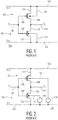
- FIG. 1 shows a Complementary Metal-Oxide Semiconductor (CMOS) device (e.g ., 40 nm and above) without body-biasing
- FIG. 2 shows the same device with biasing.
- PMOS Metal-Oxide-Semiconductor Field-Effect
- NMOS N-type Metal-Oxide-Semiconductor Field-Effect
- PMOS transistor 101 has source terminal 103 and body or substrate ("back-gate") terminal 104 coupled to positive voltage rail (V dd ) 105.
- Input (V i ) 108 of device 100 is coupled to gate terminal 106 of PMOS transistor 101 and to gate terminal 107 of NMOS transistor 102.
- Output (V o ) 111 of inverter 100 is coupled to drain terminal 109 of PMOS transistor 101 and to drain terminal 110 of NMOS transistor 102.
- Source 112 and body terminal 113 of NMOS transistor 102 are coupled to low voltage rail (V ss ) 114 ( e.g ., ground or 0 V).
- CMOS device 100 of FIG. 1 does not include a mechanism for body-biasing.
- CMOS device 120 of FIG. 2 has conventional body-biasing applied thereto.
- PMOS transistor 101 has its body terminal 104 coupled to PMOS biasing voltage source 115
- NMOS transistor 102 has its body terminal 113 coupled to NMOS biasing voltage source 116.
- CMOS device 120 may use sensing and control circuits deployed in the IC to compensate for PVT variations by applying reverse or forward body-biasing voltages 115 and 116 to body terminals 104 and 113, respectively, as a function of process and operating temperature conditions.
- Sensors may comprise process, temperature, and performance sensors distributed across the IC. The sensed data is translated into a voltage value that a biasing voltage source then applies to the body terminal of a corresponding transistor. The performance of a transistor biased in this way can be tuned by adapting the output voltage of its biasing voltage source.
- FIG. 3 is a graph illustrating relative performance versus body-biasing voltages in a conventional CMOS device, such as CMOS inverter 120 of FIG. 2 .
- the vertical axis represents the device's relative performance
- the horizontal axis an amount of body-biasing voltage applied to the substrate (or back-gate) of the device.
- Graph 300 shows three performance vs. body-biasing curves, each curve for three different operating temperatures: -40 °C (slow condition), 25 °C (normal condition), and 85 °C (fast condition).
- a PVT control algorithm works as follows.
- transistors can be speeded up by applying forward-biasing.
- transistors are inherently less leaky, as they present a higher threshold voltage V t and less electron mobility. Therefore, any leakage increase due to forward biasing has only a minimal effect on the overall energy budget.
- a slow condition can happen when operating conditions shift from the middle temperature curve (25°C), at baseline point 301, to the low temperature curve (-40 °C).
- FFB forward body-biasing
- transistors are leakier and can be made less leaky by applying reverse-biasing.
- transistors are inherently fast, as they present a lower V T and higher electron mobility). Therefore, speed degradation due to reverse biasing has minimal effect on the overall energy budget.
- a fast condition can happen when operating conditions shift from the from the middle temperature curve (25 °C), again at baseline point 301, to the elevated temperature (85 °C).
- RRB reverse body-biasing
- reverse and forward biasing can be applied by generating the appropriate voltage potential on the back-gate of a transistor with respect to the source of that transistor.
- the conventional practice is to generate the voltage potential using voltage sources 115 and/or 116.
- systems and methods described herein provide self-regulating body-bias voltage circuitry configured to compensate for PVT fluctuations in sub-threshold technologies, and particularly in FDSOI technology. It is noted that application of the same techniques to conventional CMOS transistors can lead to undesirable latch-up conditions. As the inventors hereof have recognized, however, FDSOI transistors are much more immune to latch-up because of the additional Galvanic isolation provided by a buried oxide layer. Moreover, Application of these techniques does not require additional sensors, or translation of sensor data into transistor characteristics.
- FIG. 4 is a diagram of an example of an FDSOI device with current sources controlling the application of body-biasing, according to some embodiments.
- PMOS transistor 401 and NMOS transistor402 are coupled to each otherto form FDSOI device 400 (e.g ., another logic inverter).
- PMOS transistor 401 has source terminal 403 coupled to V dd 405.
- Input (V i ) 408 of device 400 is coupled to gate terminal 406 of PMOS transistor 401 and to gate terminal 407 of NMOS transistor 402.
- Output (V o ) 411 of inverter 400 is coupled to drain terminal 409 of PMOS transistor 401 and to drain terminal 410 of NMOS transistor 402.
- source terminal 412 of NMOS transistor 402 is coupled to V ss 414.
- PMOS transistor 401 has its body terminal 404 coupled to PMOS biasing current source 415
- NMOS transistor 402 has its body terminal 413 coupled to NMOS biasing current source 416.
- FDSOI circuit 400 of FIG. 4 operates as follows: in slow conditions, the back-gates of transistors 401 and 402 are fed more current than needed for maintenance of a constant voltage (at the back-gates) by current sources 415 and 416, respectively. The voltages are adjusted on each node to allow sinking the additional currents, respectively, and therefore the transistors become automatically forward-biased. In fast conditions, the back-gates of transistors 401 and 402 are fed less current than needed for maintenance of constant voltage (at the back-gates). Therefore, the voltages are adjusted on each node to allow the conditions for the reduced currents, respectively, and therefore the transistors become automatically reverse-biased
- FIG. 5 is a graph illustrating leakage current versus body-biasing, in the case where current sources control FDSOI substrate biasing, according to some embodiments.
- the effect of slow conditions is illustrated by moving from baseline point 501 at a nominal temperature (25 °C) to a lower operating temperature curve (-40 °C), where the current needed has decreased and the back-gate of the transistor is fed more current than desired at point 502.
- the effect of fast conditions is illustrated by moving from baseline point 501 at a nominal temperature (25 °C) to a higher operating temperature curve (85 °C), where the current needed has increased and the back-gate of the transistor is fed less current than needed at point 503. This means that the automatic voltage adjustment at the back-gate adapts itself according to the PVT conditions that the transistor is exposed to.
- a high-impedance current-based driver may be used to apply a biasing-voltage to the back-gate (or body terminal) of an FDSOI transistor-by feeding a constant, fixed, or selected electrical current to the body terminal of the transistor.
- a high-impedance current source(s) continuously tries to adjust the voltage on the bulk of a transistor automatically, to keep its output current at a stable value, within suitable tolerance thresholds, therefore auto-regulating the body-biasing applied to a design and hence compensating for PVT variations.
- FIG. 6 is a diagram of an example of an FDSOI IC with body-biasing current source circuitry 601 disposed outside of IC 602, according to some embodiments.
- a first high-impedance current generator or source e.g., 416 in circuitry 601 is coupled to NMOS body-biasing pin 603, and a second high-impedance current generator or source ( e.g ., 415) in circuitry 601 is coupled to PMOS body-biasing pin 604.
- IC 602 may include internal rails configured to apply selected currents provided by body-biasing current source circuitry 601 to all transistors of interest within IC 602.
- body-biasing current sources may be placed inside the IC and may provide controlled body-bias currents to different power domains. If these currents are generated internally, depending on the PMOS or NMOS gate, the voltage supply for the current generator may be either higher or lower than conventional FDSOI supplies, respectively.
- FIG. 7 is a diagram of FDSOI IC 700 with body-biasing current sources 701 coupled to a single current bus with rails 706-708 shared across different power domains 703-705.
- body-biasing current sources 701 supply the same electrical currents (a first current for NMOS devices and a second current for PMOS devices) to all power domains that have body-biasing enabled.
- FIG. 8 is a diagram of FDSOI IC 800 with body-biasing current sources 801 coupled to each different power domain 803-805 through rails 807, 808, and 806, individually, each bus having a first rail for a first current (for NMOS devices) and a second rail current for a second current (for PMOS devices).
- FIG. 9 is a diagram of an example of current source 900 coupled to body-biasing load 907.
- NMOS transistors 901 and 902 are coupled to each other in a mirror configuration between voltage rails 904 and 906, with resistor 903 setting a reference current I ref 905, and with body-biasing load 907 drawing current I out 908 from the current mirror.
- Body biasing load 907 may be any power domain inside an IC.
- a variable output can be used instead of using a high-impedance current source with a fixed output. This gives the user the opportunity to select the amount of current and therefore the amount of PVT compensation provided with the same circuitry.
- techniques described herein enable controlling the bulk of FDSOI transistors (and hence body-biasing) by a current source, therefore automatically compensating for PVT fluctuations without the need of a dedicated monitor or sensor.
- the present techniques described herein produce very little heating and hence small temperature fluctuations.
- an electronic device may include a logic cell having a plurality of FDSOI transistors manufactured thereon, and at least one current source coupled to a body terminal of each transistor in a subset of the FDSOI transistors, where the current source is configured to output a high-impedance current.
- the at least one current source may be configurable to output a selectable high-impedance current.
- the high-impedance current may be configured to forward bias each transistor of the subset of FDSOI transistors. Additionally, or alternatively, in response to the logic cell operating at a temperature greater than a baseline temperature, the high-impedance current may be configured to reverse bias each transistor of the subset of FDSOI transistors.
- At least a subset of FDSOI transistors may include NMOS transistors and PMOS transistors, and the at least one current source may include: a first current source coupled to the body terminal of each NMOS transistor, and a second current source coupled to the body terminal of each PMOS transistor.
- the first and second current sources may be disposed outside of an integrated circuit were the logic cell is located, the first current source may be coupled to a first body-biasing rail of the logic cell, and the second current source may be coupled to a second body-biasing rail of the logic cell.
- the first and second current sources may be disposed within an integrated circuit were the logic cell is located, the logic cell includes two or more power domains, the first current source provides a first high-impedance current to the two or more power domains, and the second current source provides a second high-impedance current to the two or more power domains.
- the first and second current sources may be disposed within an integrated circuit were the logic cell is located, the logic cell includes two or more power domains, the first current source provides a first high-impedance current to a first power domain and a second high-impedance current to a second power domain, and the second current source provides a third high-impedance current to the first power domain and a fourth high-impedance current to the second power domain.
- an integrated circuit may include an FDSOI NMOS transistor having a first gate terminal, a first drain terminal, a first source terminal coupled to a first voltage rail, and a first body terminal coupled to a first current source, and an FDSOI PMOS transistor having a second gate terminal coupled to the first gate terminal, a second drain terminal coupled to the first drain terminal, a second source terminal coupled to a second voltage rail, and a second body terminal coupled to a second current source.
- the first current source may be configured to, in response to the integrated circuit operating at a temperature smaller than a baseline temperature: output a first selected current configured to forward bias the FDSOI NMOS transistor; and output a second selected current configured to forward bias the FDSOI PMOS transistor.
- the first current source may also be configured to, in response to the integrated circuit operating at a temperature greater than a baseline temperature: output a third selected current configured to reverse bias the FDSOI NMOS transistor; and output a fourth selected current configured to reverse bias the FDSOI PMOS transistor.
- the first and second current sources may be configurable to output selectable high-impedance currents.
- the first and second current sources may be disposed outside of the integrated circuit, where the first current source is coupled to a first body-biasing terminal of the integrated circuit, and where the second current source is coupled to a second body-biasing terminal of the integrated circuit.
- the first and second current sources may be disposed within the integrated circuit, where the integrated circuit further comprises two or more power domains, where the first current source provides a first selected current to the two or more power domains, and where the second current source provides a second selected current to the two or more power domains.
- the first and second current sources may be disposed within the integrated circuit, where the integrated circuit further comprises two or more power domains, where the first current source provides a first selected current to a first power domain and a second selected current to a second power domain, and where the second current source provides a third selected current to the first power domain and a fourth selected current to the second power domain.
- a method in a device having a plurality of FDSOI NMOS and PMOS transistors, may include generating a first fixed current configured to body bias the FDSOI NMOS transistors to reduce PVT fluctuations, and generating a second fixed current configured to body bias the FDSOI PMOS transistors to reduce the PVT fluctuations.
- the first fixed current may be configured to forward bias the FDSOI NMOS transistors; and in response to the device operating at a temperature greater than the baseline temperature, the first fixed current may be configured to reverse bias the FDSOI NMOS transistors.
- the second fixed current in response to the device operating at a temperature smaller than a baseline temperature, the second fixed current may be configured to forward bias the FDSOI PMOS transistors; and in response to the device operating at a temperature greater than the baseline temperature, the second fixed current may be configured to reverse bias the FDSOI PMOS transistors.
- the first and second current sources may be disposed outside of an integrated circuit were the FDSOI NMOS and PMOS transistors are located, where the first current source is coupled to a first body-biasing terminal of the device, and where the second current source is coupled to a second body-biasing terminal of the device.
- the first and second current sources may be disposed on the device were the FDSOI NMOS and PMOS transistors are located, where the device comprises two or more power domains, where the first current source provides the first fixed current to at least a first one of the two or more power domains, and where the second current source provides a second fixed current to at least the first power domain.
- an electronic device may include a logic cell having a plurality of FDSOI transistors manufactured thereon; and at least one current source coupled to a body terminal of each transistor in a subset of the FDSOI transistors, wherein the current source is configured to output a high-impedance current.
- the systems and methods disclosed herein may be incorporated into a wide range of electronic devices including, for example, computer systems or Information Technology (IT) products such as servers, desktops, laptops, memories, switches, routers, etc.; telecommunications hardware; consumer devices or appliances such as mobile phones, tablets, television sets, cameras, sound systems, etc.; scientific instrumentation; industrial robotics; medical or laboratory electronics such as imaging, diagnostic, or therapeutic equipment, etc.; transportation vehicles such as automobiles, buses, trucks, trains, watercraft, aircraft, etc.; military equipment, etc. More generally, these systems and methods may be incorporated into any device or system having one or more electronic parts or components.
- IT Information Technology
Landscapes
- Engineering & Computer Science (AREA)
- Computer Hardware Design (AREA)
- Physics & Mathematics (AREA)
- General Engineering & Computer Science (AREA)
- Theoretical Computer Science (AREA)
- Computing Systems (AREA)
- Mathematical Physics (AREA)
- Human Computer Interaction (AREA)
- General Physics & Mathematics (AREA)
- Logic Circuits (AREA)
Abstract
Description
- This disclosure relates generally to semiconductors, and more specifically, to self-regulating body-biasing techniques for Process, Voltage, and Temperature (PVT) fluctuation compensation in Fully-Depleted Silicon-on-Insulator (FDSOI) semiconductors.
- The emergence of modern technologies, such as the Internet-of-Things (loT), has created a need for devices that can operate for very long periods of time on a single battery charge. Despite many design advances (e.g., voltage scaling, power gating, clock gating, etc.), conventional semiconductors are not well-suited to meet today's low-power demands.
- Sub-threshold (or "near" sub-threshold) semiconductors consume less power than conventional semiconductors, albeit with performance trade-offs. An example of sub-threshold technology is the Fully-Depleted Silicon-on-Insulator (FDSOI) semiconductor.
- FDSOI semiconductors have an ultra-thin layer of insulator, referred to as a "buried oxide," disposed over its base silicon. In an FDSOI transistor, a very thin silicon film forms the transistor's channel. Due to the thin nature of the film, there is no need to dope the channel, and the resulting transistor is fully depleted.
- Unfortunately, sub-threshold semiconductors are particularly sensitive to Process, Voltage, and Temperature (PVT) variations. To address this problem, the inventors hereof have developed self-regulating body-biasing techniques that compensate for PVT fluctuations.
- The present invention(s) is/are illustrated by way of example and is/are not limited by the accompanying figures, in which like references indicate similar elements. Elements in the figures are illustrated for simplicity and clarity and have not necessarily been drawn to scale.
-
FIG. 1 is a diagram of a conventional Complementary Metal-Oxide Semiconductor (CMOS) device without substrate biasing. -
FIG. 2 is a diagram of a conventional CMOS device with substrate biasing. -
FIG. 3 is a graph illustrating relative performance versus body-biasing voltages in a conventional CMOS device. -
FIG. 4 is a diagram of an example of a Fully-Depleted Silicon-on-Insulator (FDSOI) device with current sources controlling the application of body-biasing, according to some embodiments. -
FIG. 5 is a graph illustrating leakage current versus body-biasing, in the case where current sources control FDSOI substrate biasing, according to some embodiments. -
FIG. 6 is a diagram of an example of an FDSOI Integrated Circuit (IC) with body-biasing current sources disposed outside the IC, according to some embodiments. -
FIG. 7 is a diagram of an example of an FDSOI IC with body-biasing current sources disposed within the IC and coupled to a current bus shared across different power domains, according to some embodiments. -
FIG. 8 is a diagram of an example of an FDSOI IC with body-biasing current sources disposed within the IC and coupled to each different power domain individually, according to some embodiments. -
FIG. 9 is a diagram of an example of a current source coupled to a body-biasing load, according to some embodiments. - Self-regulating body-biasing techniques for Process, Voltage, and Temperature (PVT) fluctuation compensation in Fully-Depleted Silicon-on-Insulator (FDSOI) semiconductors are disclosed. New sub-threshold semiconductor technologies such as 28 nm FDSOI provide the capability to tune transistors using body-biasing as an effective knob, which can significantly increase the performance of Integrated Circuits (ICs). With reduced feature sizes, however, the sensitivity of transistors and other devices to fluctuations in Process, Voltage and Temperature (PVT) becomes more evident.
- Substrate biasing, also known as body-biasing, is the use of forward and reverse bias techniques to dynamically compensate for PVT fluctuations. Conventionally, body-biasing is applied by asserting a voltage on the body (or back-bias) terminal of a transistor with respect to its source terminal.
- To illustrate the conventional approach,
FIG. 1 shows a Complementary Metal-Oxide Semiconductor (CMOS) device (e.g., 40 nm and above) without body-biasing, andFIG. 2 shows the same device with biasing. InFIG. 1 , P-type Metal-Oxide-Semiconductor Field-Effect (PMOS)transistor 101 and N-type Metal-Oxide-Semiconductor Field-Effect (NMOS)transistor 102 are coupled to each other to formCMOS device 100, here a logic inverter. - Particularly,
PMOS transistor 101 hassource terminal 103 and body or substrate ("back-gate")terminal 104 coupled to positive voltage rail (Vdd) 105. Input (Vi) 108 ofdevice 100 is coupled togate terminal 106 ofPMOS transistor 101 and togate terminal 107 ofNMOS transistor 102. Output (Vo) 111 ofinverter 100 is coupled todrain terminal 109 ofPMOS transistor 101 and to drainterminal 110 ofNMOS transistor 102.Source 112 andbody terminal 113 ofNMOS transistor 102 are coupled to low voltage rail (Vss) 114 (e.g., ground or 0 V). - As mentioned above,
CMOS device 100 ofFIG. 1 does not include a mechanism for body-biasing. In contrast,CMOS device 120 ofFIG. 2 has conventional body-biasing applied thereto. Specifically, inCMOS device 120,PMOS transistor 101 has itsbody terminal 104 coupled to PMOSbiasing voltage source 115, andNMOS transistor 102 has itsbody terminal 113 coupled to NMOSbiasing voltage source 116. - In a typical implementation,
CMOS device 120 may use sensing and control circuits deployed in the IC to compensate for PVT variations by applying reverse or forward body-biasing voltages body terminals -
FIG. 3 is a graph illustrating relative performance versus body-biasing voltages in a conventional CMOS device, such asCMOS inverter 120 ofFIG. 2 . Ingraph 300, the vertical axis represents the device's relative performance, and the horizontal axis an amount of body-biasing voltage applied to the substrate (or back-gate) of the device. Graph 300 shows three performance vs. body-biasing curves, each curve for three different operating temperatures: -40 °C (slow condition), 25 °C (normal condition), and 85 °C (fast condition). - In operation, a PVT control algorithm works as follows. In slow conditions (e.g., low temperature and/or slow process), transistors can be speeded up by applying forward-biasing. In these cases, transistors are inherently less leaky, as they present a higher threshold voltage Vt and less electron mobility. Therefore, any leakage increase due to forward biasing has only a minimal effect on the overall energy budget.
- In the context of
FIG. 3 , a slow condition can happen when operating conditions shift from the middle temperature curve (25°C), atbaseline point 301, to the low temperature curve (-40 °C). In order to recover performance, forward body-biasing (FFB) can be applied-in this case, approximately 400 mV of forward body-biasing-to maintain relative performance at "1"-now atpoint 302. - In fast conditions (e.g., high temperature and/or fast process), transistors are leakier and can be made less leaky by applying reverse-biasing. In these cases, transistors are inherently fast, as they present a lower VT and higher electron mobility). Therefore, speed degradation due to reverse biasing has minimal effect on the overall energy budget.
- Again in the context of
FIG. 3 , a fast condition can happen when operating conditions shift from the from the middle temperature curve (25 °C), again atbaseline point 301, to the elevated temperature (85 °C). In order to recover performance, reverse body-biasing (RRB) can be applied-in this case, approximately 600 mV of reverse body-biasing-to maintain relative performance at "1"-now atpoint 303.
In sum, reverse and forward biasing can be applied by generating the appropriate voltage potential on the back-gate of a transistor with respect to the source of that transistor. As illustrated inFIG. 2 , however, the conventional practice is to generate the voltage potential usingvoltage sources 115 and/or 116. - In contrast with the foregoing, systems and methods described herein provide self-regulating body-bias voltage circuitry configured to compensate for PVT fluctuations in sub-threshold technologies, and particularly in FDSOI technology. It is noted that application of the same techniques to conventional CMOS transistors can lead to undesirable latch-up conditions. As the inventors hereof have recognized, however, FDSOI transistors are much more immune to latch-up because of the additional Galvanic isolation provided by a buried oxide layer. Moreover, Application of these techniques does not require additional sensors, or translation of sensor data into transistor characteristics.
-
FIG. 4 is a diagram of an example of an FDSOI device with current sources controlling the application of body-biasing, according to some embodiments. Particularly,PMOS transistor 401 and NMOS transistor402 are coupled to each otherto form FDSOI device 400 (e.g., another logic inverter). Particularly,PMOS transistor 401 hassource terminal 403 coupled toV dd 405. Input (Vi) 408 ofdevice 400 is coupled togate terminal 406 ofPMOS transistor 401 and togate terminal 407 ofNMOS transistor 402. Output (Vo) 411 ofinverter 400 is coupled to drainterminal 409 ofPMOS transistor 401 and to drainterminal 410 ofNMOS transistor 402. Also,source terminal 412 ofNMOS transistor 402 is coupled toV ss 414. - In contrast with
CMOS device 120 ofFIG. 2 , inFDSOI device 400,PMOS transistor 401 has itsbody terminal 404 coupled to PMOS biasingcurrent source 415, andNMOS transistor 402 has itsbody terminal 413 coupled to NMOS biasingcurrent source 416. - Conventional back-biasing design practices (e.g., in
FIG. 2 ) have ignored the impact of current loading on the back-gate of the transistor due to different conditions. As the inventors hereof have determined, however, in slow conditions, the current going into the back-gate is reduced at a constant back-gate voltage. Conversely, in fast conditions, the current going into the back-gate is increased at the constant back-gate voltage. - When a high-impedance current is applied to the back-gates of
transistors FDSOI circuit 400 ofFIG. 4 operates as follows: in slow conditions, the back-gates oftransistors current sources transistors -
FIG. 5 is a graph illustrating leakage current versus body-biasing, in the case where current sources control FDSOI substrate biasing, according to some embodiments. The effect of slow conditions is illustrated by moving frombaseline point 501 at a nominal temperature (25 °C) to a lower operating temperature curve (-40 °C), where the current needed has decreased and the back-gate of the transistor is fed more current than desired atpoint 502. Conversely, the effect of fast conditions is illustrated by moving frombaseline point 501 at a nominal temperature (25 °C) to a higher operating temperature curve (85 °C), where the current needed has increased and the back-gate of the transistor is fed less current than needed atpoint 503. This means that the automatic voltage adjustment at the back-gate adapts itself according to the PVT conditions that the transistor is exposed to. - In various implementations, a high-impedance current-based driver may be used to apply a biasing-voltage to the back-gate (or body terminal) of an FDSOI transistor-by feeding a constant, fixed, or selected electrical current to the body terminal of the transistor. Such a high-impedance current source(s) continuously tries to adjust the voltage on the bulk of a transistor automatically, to keep its output current at a stable value, within suitable tolerance thresholds, therefore auto-regulating the body-biasing applied to a design and hence compensating for PVT variations.
-
FIG. 6 is a diagram of an example of an FDSOI IC with body-biasingcurrent source circuitry 601 disposed outside ofIC 602, according to some embodiments. In this case, a first high-impedance current generator or source (e.g., 416) incircuitry 601 is coupled to NMOS body-biasingpin 603, and a second high-impedance current generator or source (e.g., 415) incircuitry 601 is coupled to PMOS body-biasingpin 604.IC 602 may include internal rails configured to apply selected currents provided by body-biasingcurrent source circuitry 601 to all transistors of interest withinIC 602. - In other implementations, body-biasing current sources may be placed inside the IC and may provide controlled body-bias currents to different power domains. If these currents are generated internally, depending on the PMOS or NMOS gate, the voltage supply for the current generator may be either higher or lower than conventional FDSOI supplies, respectively.
-
FIG. 7 is a diagram ofFDSOI IC 700 with body-biasingcurrent sources 701 coupled to a single current bus with rails 706-708 shared across different power domains 703-705. In this example, body-biasingcurrent sources 701 supply the same electrical currents (a first current for NMOS devices and a second current for PMOS devices) to all power domains that have body-biasing enabled. Meanwhile,FIG. 8 is a diagram ofFDSOI IC 800 with body-biasingcurrent sources 801 coupled to each different power domain 803-805 throughrails - Many options are available for implementing high-impedance
current sources FIG. 9 is a diagram of an example ofcurrent source 900 coupled to body-biasingload 907. In this case,NMOS transistors voltage rails resistor 903 setting a reference current Iref 905, and with body-biasingload 907 drawing current Iout 908 from the current mirror.Body biasing load 907 may be any power domain inside an IC. - In other implementations, instead of using a high-impedance current source with a fixed output, a variable output can be used. This gives the user the opportunity to select the amount of current and therefore the amount of PVT compensation provided with the same circuitry.
- As described above, in various embodiments, techniques described herein enable controlling the bulk of FDSOI transistors (and hence body-biasing) by a current source, therefore automatically compensating for PVT fluctuations without the need of a dedicated monitor or sensor. In contrast with conventional body bias schemes discussed previously, the present techniques described herein produce very little heating and hence small temperature fluctuations. These techniques may be applied to all FDSOI designs that benefit from body-biasing, including, but not limited to, microprocessors, microcontrollers, Graphics Processing Units (GPUs), Digital Signal Processors (DSPs), memories, etc. With future envisioned loT products, cost (i.e., die area) and power consumption can be significantly reduced.
- In an illustrative, non-limiting embodiment, an electronic device may include a logic cell having a plurality of FDSOI transistors manufactured thereon, and at least one current source coupled to a body terminal of each transistor in a subset of the FDSOI transistors, where the current source is configured to output a high-impedance current. The at least one current source may be configurable to output a selectable high-impedance current.
- In response to the logic cell operating at a temperature smallerthan a baseline temperature, the high-impedance current may be configured to forward bias each transistor of the subset of FDSOI transistors. Additionally, or alternatively, in response to the logic cell operating at a temperature greater than a baseline temperature, the high-impedance current may be configured to reverse bias each transistor of the subset of FDSOI transistors.
- At least a subset of FDSOI transistors may include NMOS transistors and PMOS transistors, and the at least one current source may include: a first current source coupled to the body terminal of each NMOS transistor, and a second current source coupled to the body terminal of each PMOS transistor.
- In some cases, the first and second current sources may be disposed outside of an integrated circuit were the logic cell is located, the first current source may be coupled to a first body-biasing rail of the logic cell, and the second current source may be coupled to a second body-biasing rail of the logic cell.
- In other cases, the first and second current sources may be disposed within an integrated circuit were the logic cell is located, the logic cell includes two or more power domains, the first current source provides a first high-impedance current to the two or more power domains, and the second current source provides a second high-impedance current to the two or more power domains.
- In yet other cases, the first and second current sources may be disposed within an integrated circuit were the logic cell is located, the logic cell includes two or more power domains, the first current source provides a first high-impedance current to a first power domain and a second high-impedance current to a second power domain, and the second current source provides a third high-impedance current to the first power domain and a fourth high-impedance current to the second power domain.
- In another illustrative, non-limiting embodiment, an integrated circuit may include an FDSOI NMOS transistor having a first gate terminal, a first drain terminal, a first source terminal coupled to a first voltage rail, and a first body terminal coupled to a first current source, and an FDSOI PMOS transistor having a second gate terminal coupled to the first gate terminal, a second drain terminal coupled to the first drain terminal, a second source terminal coupled to a second voltage rail, and a second body terminal coupled to a second current source.
- The first current source may be configured to, in response to the integrated circuit operating at a temperature smaller than a baseline temperature: output a first selected current configured to forward bias the FDSOI NMOS transistor; and output a second selected current configured to forward bias the FDSOI PMOS transistor.
- The first current source may also be configured to, in response to the integrated circuit operating at a temperature greater than a baseline temperature: output a third selected current configured to reverse bias the FDSOI NMOS transistor; and output a fourth selected current configured to reverse bias the FDSOI PMOS transistor.
- The first and second current sources may be configurable to output selectable high-impedance currents. In some cases, the first and second current sources may be disposed outside of the integrated circuit, where the first current source is coupled to a first body-biasing terminal of the integrated circuit, and where the second current source is coupled to a second body-biasing terminal of the integrated circuit. In other cases, the first and second current sources may be disposed within the integrated circuit, where the integrated circuit further comprises two or more power domains, where the first current source provides a first selected current to the two or more power domains, and where the second current source provides a second selected current to the two or more power domains. In yet other cases, the first and second current sources may be disposed within the integrated circuit, where the integrated circuit further comprises two or more power domains, where the first current source provides a first selected current to a first power domain and a second selected current to a second power domain, and where the second current source provides a third selected current to the first power domain and a fourth selected current to the second power domain.
- In yet another illustrative, non-limiting embodiment, in a device having a plurality of FDSOI NMOS and PMOS transistors, a method may include generating a first fixed current configured to body bias the FDSOI NMOS transistors to reduce PVT fluctuations, and generating a second fixed current configured to body bias the FDSOI PMOS transistors to reduce the PVT fluctuations.
- In response to the device operating at a temperature smaller than a baseline temperature, the first fixed current may be configured to forward bias the FDSOI NMOS transistors; and in response to the device operating at a temperature greater than the baseline temperature, the first fixed current may be configured to reverse bias the FDSOI NMOS transistors. Additionally, or alternatively, in response to the device operating at a temperature smaller than a baseline temperature, the second fixed current may be configured to forward bias the FDSOI PMOS transistors; and in response to the device operating at a temperature greater than the baseline temperature, the second fixed current may be configured to reverse bias the FDSOI PMOS transistors.
- In some cases, the first and second current sources may be disposed outside of an integrated circuit were the FDSOI NMOS and PMOS transistors are located, where the first current source is coupled to a first body-biasing terminal of the device, and where the second current source is coupled to a second body-biasing terminal of the device. In other case, the first and second current sources may be disposed on the device were the FDSOI NMOS and PMOS transistors are located, where the device comprises two or more power domains, where the first current source provides the first fixed current to at least a first one of the two or more power domains, and where the second current source provides a second fixed current to at least the first power domain.
- Self-regulating body-biasing techniques for Process, Voltage, and Temperature (PVT) fluctuation compensation in Fully-Depleted Silicon-on-Insulator (FDSOI) semiconductors are disclosed. In an illustrative, non-limiting embodiment, an electronic device may include a logic cell having a plurality of FDSOI transistors manufactured thereon; and at least one current source coupled to a body terminal of each transistor in a subset of the FDSOI transistors, wherein the current source is configured to output a high-impedance current.
- In many implementations, the systems and methods disclosed herein may be incorporated into a wide range of electronic devices including, for example, computer systems or Information Technology (IT) products such as servers, desktops, laptops, memories, switches, routers, etc.; telecommunications hardware; consumer devices or appliances such as mobile phones, tablets, television sets, cameras, sound systems, etc.; scientific instrumentation; industrial robotics; medical or laboratory electronics such as imaging, diagnostic, or therapeutic equipment, etc.; transportation vehicles such as automobiles, buses, trucks, trains, watercraft, aircraft, etc.; military equipment, etc. More generally, these systems and methods may be incorporated into any device or system having one or more electronic parts or components.
- Although the invention(s) is/are described herein with reference to specific embodiments, various modifications and changes can be made without departing from the scope of the present invention(s), as set forth in the claims below. Accordingly, the specification and figures are to be regarded in an illustrative rather than a restrictive sense, and all such modifications are intended to be included within the scope of the present invention(s). Any benefits, advantages, or solutions to problems that are described herein with regard to specific embodiments are not intended to be construed as a critical, required, or essential feature or element of any or all the claims.
- Unless stated otherwise, terms such as "first" and "second" are used to arbitrarily distinguish between the elements such terms describe. Thus, these terms are not necessarily intended to indicate temporal or other prioritization of such elements. The terms "coupled" or "operably coupled" are defined as connected, although not necessarily directly, and not necessarily mechanically. The terms "a" and "an" are defined as one or more unless stated otherwise. The terms "comprise" (and any form of comprise, such as "comprises" and "comprising"), "have" (and any form of have, such as "has" and "having"), "include" (and any form of include, such as "includes" and "including") and "contain" (and any form of contain, such as "contains" and "containing") are open-ended linking verbs. As a result, a system, device, or apparatus that "comprises," "has," "includes" or "contains" one or more elements possesses those one or more elements but is not limited to possessing only those one or more elements. Similarly, a method or process that "comprises," "has," "includes" or "contains" one or more operations possesses those one or more operations but is not limited to possessing only those one or more operations.
Claims (13)
- An electronic device, comprising:a logic cell having a plurality of Fully-Depleted Silicon-on-Insulator (FDSOI) transistors manufactured thereon; andat least one current source coupled to a body terminal of each transistor in a subset of the FDSOI transistors, wherein the current source is configured to output a high-impedance current.
- The electronic device of claim 1, wherein in response to the logic cell operating at a temperature smaller than a baseline temperature, the high-impedance current is configured to forward bias each transistor of the subset of FDSOI transistors.
- The electronic device of claim 1 or 2, wherein in response to the logic cell operating at a temperature greater than a baseline temperature, the high-impedance current is configured to reverse bias each transistor of the subset of FDSOI transistors.
- The electronic device of any preceding claim, wherein the subset of FDSOI transistors comprises N-type Metal-Oxide-Semiconductor Field-Effect (NMOS) transistors and P-type Metal-Oxide-Semiconductor Field-Effect (PMOS) transistors, and wherein the at least one current source further comprises:a first current source coupled to the body terminal of each NMOS transistor; anda second current source coupled to the body terminal of each PMOS transistor.
- The electronic device of claim 4, wherein the first and second current sources are disposed outside of an integrated circuit were the logic cell is located, wherein the first current source is coupled to a first body-biasing rail of the logic cell, and wherein the second current source is coupled to a second body-biasing rail of the logic cell.
- The electronic device of claim 4 or 5, wherein the first and second current sources are disposed within an integrated circuit were the logic cell is located, wherein the logic cell comprises two or more power domains, wherein the first current source provides a first high-impedance current to the two or more power domains, and wherein the second current source provides a second high-impedance current to the two or more power domains.
- The electronic device of any of claims 4 to 6, wherein the first and second current sources are disposed within an integrated circuit were the logic cell is located, wherein the logic cell comprises two or more power domains, wherein the first current source provides a first high-impedance current to a first power domain and a second high-impedance current to a second power domain, and wherein the second current source provides a third high-impedance current to the first power domain and a fourth high-impedance current to the second power domain.
- The electronic device of any of claims 4 to 7, wherein the at least one current source is configurable to output a selectable high-impedance current.
- A method, comprising:
in a device having a plurality of Fully-Depleted Silicon-on-Insulator (FDSOI) N-type Metal-Oxide-Semiconductor Field-Effect (NMOS) and P-type Metal-Oxide-Semiconductor Field-Effect (PMOS) transistors,(i) generating a first fixed current configured to body bias the FDSOI NMOS transistors to reduce Process, Voltage, and Temperature (PVT) fluctuations; and(ii) generating a second fixed current configured to body bias the FDSOI PMOS transistors to reduce the PVT fluctuations. - The method of claim 9, wherein:in response to the device operating at a temperature smaller than a baseline temperature, the first fixed current is configured to forward bias the FDSOI NMOS transistors; andin response to the device operating at a temperature greater than the baseline temperature, the first fixed current is configured to reverse bias the FDSOI NMOS transistors.
- The method of claim 9 or 10, wherein:in response to the device operating at a temperature smaller than a baseline temperature, the second fixed current is configured to forward bias the FDSOI PMOS transistors; andin response to the device operating at a temperature greater than the baseline temperature, the second fixed current is configured to reverse bias the FDSOI PMOS transistors.
- The method of any of claims 9 to 11, wherein the first and second current sources are disposed outside of an integrated circuit were the FDSOI NMOS and PMOS transistors are located, wherein the first current source is coupled to a first body-biasing terminal of the device, and wherein the second current source is coupled to a second body-biasing terminal of the device.
- The method of any of claims 9 to 12, wherein the first and second current sources are disposed on the device were the FDSOI NMOS and PMOS transistors are located, wherein the device comprises two or more power domains, wherein the first current source provides the first fixed current to at least a first one of the two or more power domains, and wherein the second current source provides a second fixed current to at least the first power domain.
Applications Claiming Priority (1)
| Application Number | Priority Date | Filing Date | Title |
|---|---|---|---|
| US16/404,931 US10819331B1 (en) | 2019-05-07 | 2019-05-07 | Self-regulating body-biasing techniques for process, voltage, and temperature (PVT) fluctuation compensation in fully-depleted silicon-on-insulator (FDSOI) semiconductors |
Publications (1)
| Publication Number | Publication Date |
|---|---|
| EP3736664A1 true EP3736664A1 (en) | 2020-11-11 |
Family
ID=70613652
Family Applications (1)
| Application Number | Title | Priority Date | Filing Date |
|---|---|---|---|
| EP20173265.8A Pending EP3736664A1 (en) | 2019-05-07 | 2020-05-06 | Self-regulating body-biasing techniques for process, voltage, and temperature (pvt) fluctuation compensation in fully-depleted silicon-on-insulator (fdsoi) semiconductors |
Country Status (2)
| Country | Link |
|---|---|
| US (1) | US10819331B1 (en) |
| EP (1) | EP3736664A1 (en) |
Families Citing this family (3)
| Publication number | Priority date | Publication date | Assignee | Title |
|---|---|---|---|---|
| JP7297549B2 (en) * | 2019-06-21 | 2023-06-26 | エイブリック株式会社 | VOLTAGE-CURRENT CONVERSION CIRCUIT AND CHARGE/DISCHARGE CONTROL DEVICE |
| US11921651B2 (en) * | 2021-06-07 | 2024-03-05 | AyDeeKay LLC | Interface module with low-latency communication of electrical signals between power domains |
| CN119995530B (en) * | 2025-01-16 | 2025-11-07 | 杭州电子科技大学 | A PVT-compensated ultra-low voltage fully differential OTA amplifier based on an inverter |
Citations (4)
| Publication number | Priority date | Publication date | Assignee | Title |
|---|---|---|---|---|
| US20020029352A1 (en) * | 1998-12-30 | 2002-03-07 | Shekhar Y. Borkar | Software control of transistor body bias in controlling chip parameters |
| US20090070772A1 (en) * | 2007-09-11 | 2009-03-12 | Hitachi, Ltd. | Multiprocessor system |
| US20160094217A1 (en) * | 2014-09-29 | 2016-03-31 | Stmicroelectronics International N.V. | Driver circuit including driver transistors with controlled body biasing |
| US20170098474A1 (en) * | 2015-10-05 | 2017-04-06 | Silicon Storage Technology, Inc. | Fully Depleted Silicon On Insulator Flash Memory Design |
Family Cites Families (5)
| Publication number | Priority date | Publication date | Assignee | Title |
|---|---|---|---|---|
| US5486788A (en) * | 1994-10-07 | 1996-01-23 | Sgs-Thomson Microelectronics, Inc. | Chopper stabilized operational transconductance amplifier |
| US7649402B1 (en) | 2003-12-23 | 2010-01-19 | Tien-Min Chen | Feedback-controlled body-bias voltage source |
| US7397231B2 (en) * | 2006-07-25 | 2008-07-08 | Power Integrations, Inc. | Method and apparatus for adjusting a reference |
| US9264045B2 (en) * | 2014-04-01 | 2016-02-16 | Stmicroelectronics International N.V. | Buffer circuit with reduced static leakage through controlled body biasing in FDSOI technology |
| US9837439B1 (en) * | 2016-08-12 | 2017-12-05 | Globalfoundries Inc. | Compensation of temperature effects in semiconductor device structures |
-
2019
- 2019-05-07 US US16/404,931 patent/US10819331B1/en active Active
-
2020
- 2020-05-06 EP EP20173265.8A patent/EP3736664A1/en active Pending
Patent Citations (4)
| Publication number | Priority date | Publication date | Assignee | Title |
|---|---|---|---|---|
| US20020029352A1 (en) * | 1998-12-30 | 2002-03-07 | Shekhar Y. Borkar | Software control of transistor body bias in controlling chip parameters |
| US20090070772A1 (en) * | 2007-09-11 | 2009-03-12 | Hitachi, Ltd. | Multiprocessor system |
| US20160094217A1 (en) * | 2014-09-29 | 2016-03-31 | Stmicroelectronics International N.V. | Driver circuit including driver transistors with controlled body biasing |
| US20170098474A1 (en) * | 2015-10-05 | 2017-04-06 | Silicon Storage Technology, Inc. | Fully Depleted Silicon On Insulator Flash Memory Design |
Non-Patent Citations (1)
| Title |
|---|
| KILIC MUSTAFA ET AL: "A hybrid CDAC-threshold configuring SAR ADC in 28nm FDSOI CMOS", ANALOG INTEGRATED CIRCUITS AND SIGNAL PROCESSING, SPRINGER NEW YORK LLC, US, vol. 97, no. 3, 12 June 2018 (2018-06-12), pages 397 - 404, XP036631705, ISSN: 0925-1030, [retrieved on 20180612], DOI: 10.1007/S10470-018-1222-5 * |
Also Published As
| Publication number | Publication date |
|---|---|
| US10819331B1 (en) | 2020-10-27 |
| US20200358435A1 (en) | 2020-11-12 |
Similar Documents
| Publication | Publication Date | Title |
|---|---|---|
| US6087893A (en) | Semiconductor integrated circuit having suppressed leakage currents | |
| US8610488B2 (en) | 3X input voltage tolerant device and circuit | |
| US5406140A (en) | Voltage translation and overvoltage protection | |
| US5461338A (en) | Semiconductor integrated circuit incorporated with substrate bias control circuit | |
| KR100220899B1 (en) | Cmos substrate biasing for threshold voltage control | |
| US6177826B1 (en) | Silicon-on-insulator circuit having series connected PMOS transistors each having connected body and gate | |
| EP0702860B1 (en) | Overvoltage protection | |
| CN101662277B (en) | Adaptive voltage bias control system and integrated circuit | |
| US8299847B2 (en) | Semiconductor device and data processing system including the same | |
| US10819331B1 (en) | Self-regulating body-biasing techniques for process, voltage, and temperature (PVT) fluctuation compensation in fully-depleted silicon-on-insulator (FDSOI) semiconductors | |
| US5017811A (en) | CMOS TTL input buffer using a ratioed inverter with a threshold voltage adjusted N channel field effect transistor | |
| US20090080276A1 (en) | Temperature Dependent Bias for Minimal Stand-by Power in CMOS Circuits | |
| KR920006014B1 (en) | How to increase input buffer and threshold voltage | |
| US20040014268A1 (en) | Semiconductor integrated circuit device having body biasing circuit for generating forward well bias voltage of suitable level by using simple circuitry | |
| US11004843B2 (en) | Switch control circuit for a power switch with electrostatic discharge (ESD) protection | |
| US11029216B1 (en) | IC with stragically biased digital circuitry | |
| EP2557479A2 (en) | Adjustable body bias circuit | |
| EP1743423B1 (en) | Threshold voltage adjustment in thin film transistors | |
| US9177622B2 (en) | Supply independent delayer | |
| US9494987B2 (en) | Processing system with low power wake-up pad | |
| US10153768B1 (en) | Integrated circuitry and methods for reducing leakage current | |
| US20150145564A1 (en) | Electronic Switching Device with Reduction of Leakage Currents and Corresponding Control Method | |
| US9071248B2 (en) | MOS transistor drain-to-gate leakage protection circuit and method therefor | |
| US6636073B2 (en) | Semiconductor integrated circuit | |
| US9110484B2 (en) | Temperature dependent biasing for leakage power reduction |
Legal Events
| Date | Code | Title | Description |
|---|---|---|---|
| PUAI | Public reference made under article 153(3) epc to a published international application that has entered the european phase |
Free format text: ORIGINAL CODE: 0009012 |
|
| STAA | Information on the status of an ep patent application or granted ep patent |
Free format text: STATUS: THE APPLICATION HAS BEEN PUBLISHED |
|
| AK | Designated contracting states |
Kind code of ref document: A1 Designated state(s): AL AT BE BG CH CY CZ DE DK EE ES FI FR GB GR HR HU IE IS IT LI LT LU LV MC MK MT NL NO PL PT RO RS SE SI SK SM TR |
|
| AX | Request for extension of the european patent |
Extension state: BA ME |
|
| STAA | Information on the status of an ep patent application or granted ep patent |
Free format text: STATUS: REQUEST FOR EXAMINATION WAS MADE |
|
| 17P | Request for examination filed |
Effective date: 20210511 |
|
| RBV | Designated contracting states (corrected) |
Designated state(s): AL AT BE BG CH CY CZ DE DK EE ES FI FR GB GR HR HU IE IS IT LI LT LU LV MC MK MT NL NO PL PT RO RS SE SI SK SM TR |
|
| STAA | Information on the status of an ep patent application or granted ep patent |
Free format text: STATUS: EXAMINATION IS IN PROGRESS |
|
| 17Q | First examination report despatched |
Effective date: 20230425 |