EP3734647A1 - A driving circuit of a power circuit and a package structure thereof - Google Patents
A driving circuit of a power circuit and a package structure thereof Download PDFInfo
- Publication number
- EP3734647A1 EP3734647A1 EP19218337.4A EP19218337A EP3734647A1 EP 3734647 A1 EP3734647 A1 EP 3734647A1 EP 19218337 A EP19218337 A EP 19218337A EP 3734647 A1 EP3734647 A1 EP 3734647A1
- Authority
- EP
- European Patent Office
- Prior art keywords
- transistor
- sub
- supply voltage
- voltage
- driving
- Prior art date
- Legal status (The legal status is an assumption and is not a legal conclusion. Google has not performed a legal analysis and makes no representation as to the accuracy of the status listed.)
- Granted
Links
Images









Classifications
-
- G—PHYSICS
- G11—INFORMATION STORAGE
- G11C—STATIC STORES
- G11C5/00—Details of stores covered by group G11C11/00
- G11C5/14—Power supply arrangements, e.g. power down, chip selection or deselection, layout of wirings or power grids, or multiple supply levels
- G11C5/145—Applications of charge pumps; Boosted voltage circuits; Clamp circuits therefor
-
- H—ELECTRICITY
- H03—ELECTRONIC CIRCUITRY
- H03K—PULSE TECHNIQUE
- H03K17/00—Electronic switching or gating, i.e. not by contact-making and –breaking
- H03K17/06—Modifications for ensuring a fully conducting state
- H03K17/063—Modifications for ensuring a fully conducting state in field-effect transistor switches
-
- H—ELECTRICITY
- H03—ELECTRONIC CIRCUITRY
- H03K—PULSE TECHNIQUE
- H03K17/00—Electronic switching or gating, i.e. not by contact-making and –breaking
- H03K17/51—Electronic switching or gating, i.e. not by contact-making and –breaking characterised by the components used
- H03K17/56—Electronic switching or gating, i.e. not by contact-making and –breaking characterised by the components used by the use, as active elements, of semiconductor devices
- H03K17/687—Electronic switching or gating, i.e. not by contact-making and –breaking characterised by the components used by the use, as active elements, of semiconductor devices the devices being field-effect transistors
- H03K17/6871—Electronic switching or gating, i.e. not by contact-making and –breaking characterised by the components used by the use, as active elements, of semiconductor devices the devices being field-effect transistors the output circuit comprising more than one controlled field-effect transistor
-
- H—ELECTRICITY
- H10—SEMICONDUCTOR DEVICES; ELECTRIC SOLID-STATE DEVICES NOT OTHERWISE PROVIDED FOR
- H10W—GENERIC PACKAGES, INTERCONNECTIONS, CONNECTORS OR OTHER CONSTRUCTIONAL DETAILS OF DEVICES COVERED BY CLASS H10
- H10W70/00—Package substrates; Interposers; Redistribution layers [RDL]
- H10W70/01—Manufacture or treatment
- H10W70/05—Manufacture or treatment of insulating or insulated package substrates, or of interposers, or of redistribution layers
- H10W70/08—Manufacture or treatment of insulating or insulated package substrates, or of interposers, or of redistribution layers by depositing layers on the chip or wafer, e.g. "chip-first" RDLs
- H10W70/09—Manufacture or treatment of insulating or insulated package substrates, or of interposers, or of redistribution layers by depositing layers on the chip or wafer, e.g. "chip-first" RDLs extending onto an encapsulation that laterally surrounds the chip or wafer, e.g. fan-out wafer level package [FOWLP] RDLs
-
- H—ELECTRICITY
- H10—SEMICONDUCTOR DEVICES; ELECTRIC SOLID-STATE DEVICES NOT OTHERWISE PROVIDED FOR
- H10W—GENERIC PACKAGES, INTERCONNECTIONS, CONNECTORS OR OTHER CONSTRUCTIONAL DETAILS OF DEVICES COVERED BY CLASS H10
- H10W90/00—Package configurations
-
- G—PHYSICS
- G11—INFORMATION STORAGE
- G11C—STATIC STORES
- G11C5/00—Details of stores covered by group G11C11/00
- G11C5/14—Power supply arrangements, e.g. power down, chip selection or deselection, layout of wirings or power grids, or multiple supply levels
- G11C5/142—Contactless power supplies, e.g. RF, induction, or IR
-
- H—ELECTRICITY
- H03—ELECTRONIC CIRCUITRY
- H03K—PULSE TECHNIQUE
- H03K2217/00—Indexing scheme related to electronic switching or gating, i.e. not by contact-making or -breaking covered by H03K17/00
- H03K2217/0063—High side switches, i.e. the higher potential [DC] or life wire [AC] being directly connected to the switch and not via the load
-
- H—ELECTRICITY
- H03—ELECTRONIC CIRCUITRY
- H03K—PULSE TECHNIQUE
- H03K2217/00—Indexing scheme related to electronic switching or gating, i.e. not by contact-making or -breaking covered by H03K17/00
- H03K2217/0072—Low side switches, i.e. the lower potential [DC] or neutral wire [AC] being directly connected to the switch and not via the load
-
- H—ELECTRICITY
- H03—ELECTRONIC CIRCUITRY
- H03K—PULSE TECHNIQUE
- H03K2217/00—Indexing scheme related to electronic switching or gating, i.e. not by contact-making or -breaking covered by H03K17/00
- H03K2217/0081—Power supply means, e.g. to the switch driver
-
- H—ELECTRICITY
- H10—SEMICONDUCTOR DEVICES; ELECTRIC SOLID-STATE DEVICES NOT OTHERWISE PROVIDED FOR
- H10W—GENERIC PACKAGES, INTERCONNECTIONS, CONNECTORS OR OTHER CONSTRUCTIONAL DETAILS OF DEVICES COVERED BY CLASS H10
- H10W70/00—Package substrates; Interposers; Redistribution layers [RDL]
- H10W70/099—Connecting interconnections to insulating or insulated package substrates, interposers or redistribution layers
-
- H—ELECTRICITY
- H10—SEMICONDUCTOR DEVICES; ELECTRIC SOLID-STATE DEVICES NOT OTHERWISE PROVIDED FOR
- H10W—GENERIC PACKAGES, INTERCONNECTIONS, CONNECTORS OR OTHER CONSTRUCTIONAL DETAILS OF DEVICES COVERED BY CLASS H10
- H10W72/00—Interconnections or connectors in packages
- H10W72/071—Connecting or disconnecting
- H10W72/073—Connecting or disconnecting of die-attach connectors
-
- H—ELECTRICITY
- H10—SEMICONDUCTOR DEVICES; ELECTRIC SOLID-STATE DEVICES NOT OTHERWISE PROVIDED FOR
- H10W—GENERIC PACKAGES, INTERCONNECTIONS, CONNECTORS OR OTHER CONSTRUCTIONAL DETAILS OF DEVICES COVERED BY CLASS H10
- H10W72/00—Interconnections or connectors in packages
- H10W72/30—Die-attach connectors
- H10W72/351—Materials of die-attach connectors
- H10W72/352—Materials of die-attach connectors comprising metals or metalloids, e.g. solders
-
- H—ELECTRICITY
- H10—SEMICONDUCTOR DEVICES; ELECTRIC SOLID-STATE DEVICES NOT OTHERWISE PROVIDED FOR
- H10W—GENERIC PACKAGES, INTERCONNECTIONS, CONNECTORS OR OTHER CONSTRUCTIONAL DETAILS OF DEVICES COVERED BY CLASS H10
- H10W72/00—Interconnections or connectors in packages
- H10W72/851—Dispositions of multiple connectors or interconnections
- H10W72/874—On different surfaces
-
- H—ELECTRICITY
- H10—SEMICONDUCTOR DEVICES; ELECTRIC SOLID-STATE DEVICES NOT OTHERWISE PROVIDED FOR
- H10W—GENERIC PACKAGES, INTERCONNECTIONS, CONNECTORS OR OTHER CONSTRUCTIONAL DETAILS OF DEVICES COVERED BY CLASS H10
- H10W72/00—Interconnections or connectors in packages
- H10W72/90—Bond pads, in general
- H10W72/941—Dispositions of bond pads
- H10W72/9413—Dispositions of bond pads on encapsulations
-
- H—ELECTRICITY
- H10—SEMICONDUCTOR DEVICES; ELECTRIC SOLID-STATE DEVICES NOT OTHERWISE PROVIDED FOR
- H10W—GENERIC PACKAGES, INTERCONNECTIONS, CONNECTORS OR OTHER CONSTRUCTIONAL DETAILS OF DEVICES COVERED BY CLASS H10
- H10W90/00—Package configurations
- H10W90/701—Package configurations characterised by the relative positions of pads or connectors relative to package parts
- H10W90/731—Package configurations characterised by the relative positions of pads or connectors relative to package parts of die-attach connectors
- H10W90/736—Package configurations characterised by the relative positions of pads or connectors relative to package parts of die-attach connectors between a chip and a stacked lead frame, conducting package substrate or heat sink
Definitions
- the disclosure relates generally to driving circuits and isolators integrated with GaN power transistors, and more specifically it relates to a package structure including the driving circuits, isolators, and GaN power transistors.
- a charge pump is always required to boost the supply voltage to a higher voltage for driving the power transistor.
- Fig. 1 illustrates a conventional power circuit.
- the high-side driver DRV1 is configured to drive the first power transistor 110A
- the low-side driver DRV2 is configured to drive the second power transistor 110B.
- the boost capacitor CB and the boost diode DB are configured to boost the supply voltage VDD to the boost voltage VB, so that the first power transistor 110A can be fully turned on. Therefore, the first power transistor 110A supplied with the input voltage VIN and the second power transistor 110B can drive the load device RL through the inductor L and the capacitor C.
- the inductor L may induce significant parasitic effects at the switch node SW (such as a negative voltage spike generated at the switch node SW by the turned-on body diode of the second power transistor 110B), these parasitic effects can interfere with the boost voltage VB when the boost capacitor CB is charged through the power transistor. Therefore, it is necessary to eliminate parasitic effects from the driving circuit.
- an integrated circuit comprises a first power transistor, a second power transistor, and an isolator.
- the first power transistor is integrated with a first driving circuit.
- the second power transistor is integrated with a second driving circuit.
- the isolator provides a first control signal and a second control signal to the first power transistor and a second power transistor respectively, according to an input signal.
- the integrated circuit further comprises a first power circuit and a second power circuit, wherein the first power circuit comprises the first driving circuit and the first power transistor, wherein the second power circuit comprises the second driving circuit and the second power transistor.
- the integrated circuit further comprises a bootstrap diode and a bootstrap capacitor.
- the bootstrap diode comprises a bootstrap anode and a bootstrap cathode, wherein the bootstrap anode is coupled to a first supply voltage and the bootstrap cathode is coupled to a second supply voltage.
- the bootstrap capacitor is coupled between the second supply voltage and a switch voltage of a switch node.
- the first driving circuit is supplied by the second supply voltage and the switch voltage and generates a first driving voltage at a first driving node according to the first control signal.
- the first power transistor supplies a high voltage to the switch node according to the first driving voltage.
- the second driving circuit is supplied by the first supply voltage and a first ground and generates a second driving voltage at a second driving node according to the second control signal.
- the second power transistor pulls the switch voltage down to the first ground according to the second driving voltage.
- each of the first power transistor and the second power transistor is a GaN transistor.
- the high voltage exceeds the first supply voltage and the second supply voltage.
- the isolator comprises a first sub-isolator and a second sub-isolator.
- the first sub-isolator comprises a first transmitter, a first receiver, and a first isolation barrier.
- the first transmitter is supplied with a third supply voltage and a second ground and transmits a first radio signal according to the input signal.
- the first receiver is supplied with the second supply voltage and the switch voltage and generates the first control signal according to the first radio signal.
- the first isolation barrier is configured to electrically isolate the first transmitter from the first receiver.
- the second sub-isolator comprises a second transmitter, a second receiver, and a second isolation barrier.
- the second transmitter is supplied with a third supply voltage and a second ground and transmits a second radio signal according to the input signal.
- the second receiver is supplied with the first supply voltage and the first ground and generates the first control signal according to the first radio signal.
- the second isolation barrier is configured to electrically isolate the second transmitter from the second receiver.
- the isolator comprises: a transmitter, a first receiver, a first isolation barrier, a second receiver, and a second isolation barrier.
- the transmitter is supplied with a third supply voltage and a second ground and transmits a first radio signal and a second radio signal according to the input signal.
- the first receiver is supplied with the second supply voltage and the switch voltage and generates the first control signal according to the first radio signal.
- the first isolation barrier is configured to electrically isolate the transmitter from the first receiver.
- the second receiver is supplied with the first supply voltage and the first ground and generates the first control signal according to the first radio signal.
- the second isolation barrier is configured to electrically isolate the transmitter from the second receiver.
- the integrated circuit further comprises a decoupling capacitor.
- the decoupling capacitor is coupled between the high voltage and the first ground, wherein the first sub-isolator, the second sub-isolator, the first power circuit, a second power circuit, and the decoupling capacitor are packaged together.
- each of the first power circuit and the second power circuit comprises a pre-driver.
- the pre-driver generates a first internal signal according to the control signal, wherein the pre-driver is configured to improve driving capability of the control signal, wherein the driving circuit generates the driving voltage according to the first internal signal.
- each of the first driving circuit and the second driving circuit comprises a high-side transistor, a low-side transistor, and a charge pump.
- the high-side transistor provides a supply voltage to a driving node according to a high-side voltage of a high-side node.
- the low-side transistor couples the driving node to the ground according to a first internal signal.
- the charge pump is coupled to the high-side node and the driving node, wherein the charge pump is configured to generate a high-side voltage that exceeds the supply voltage according to the first internal signal.
- each of the first power circuit and the second power circuit comprises a hysteresis circuit.
- the hysteresis circuit is coupled between the control signal and the pre-driver, wherein the hysteresis circuit receives the control signal to generate a second internal signal, such that the pre-driver generates the first internal signal according to the second internal signal, wherein the hysteresis circuit is configured to provide a hysteresis for the control signal.
- the hysteresis circuit comprises a first resistor, a third normally-off transistor, a fourth normally-off transistor, a fifth normally-off transistor, and a second resistor.
- the first resistor is coupled between the supply voltage and an output node, wherein the second internal signal is generated at the output node.
- the third normally-off transistor comprises a gate terminal coupled to a third node, a source terminal coupled to a fourth node, and a drain terminal coupled to the output node.
- the fourth normally-off transistor comprises a gate terminal coupled to the third node, a source terminal coupled to the ground, and a drain terminal coupled to the fourth node.
- the fifth normally-off transistor comprises a gate terminal coupled to the output node, a source terminal coupled to the fourth node, and a drain terminal supplied by the supply voltage.
- the second resistor is coupled to the third node and receives the control signal.
- the pre-driver comprises a first sub pre-driver, a second sub pre-driver, a third sub pre-driver, and a fourth sub pre-driver.
- the first sub pre-driver generates the first internal signal according to a first sub-internal signal.
- the second sub pre-driver generates the first sub-internal signal according to a second sub-internal signal.
- the third sub pre-driver generates the second sub-internal signal according to a third internal signal.
- the fourth sub pre-driver generates the third sub-internal signal according to the second internal signal.
- the first sub pre-driver comprises: a first sub normally-off transistor, a second sub normally-off transistor, and a first sub normally-on transistor.
- the first sub normally-off transistor comprises a gate terminal receiving the first sub-internal signal, a source terminal coupled to the ground, and a drain terminal generating the first internal signal.
- the second sub normally-off transistor comprises a gate terminal receiving the second sub-internal signal, a source terminal coupled to the drain terminal of the first sub normally-off transistor, and a drain terminal supplied with the supply voltage.
- the first sub normally-on transistor comprises a gate terminal coupled to the drain terminal of the first sub normally-off transistor, a source terminal coupled to the drain terminal of the first sub normally-off transistor, and a drain terminal supplied with the supply voltage.
- the second sub pre-driver comprises: a third sub normally-off transistor, a fourth sub normally-off transistor, and a second sub normally-on transistor.
- the third sub normally-off transistor comprises a gate terminal receiving the second sub-internal signal, a source terminal coupled to the ground, and a drain terminal generating the first sub-internal signal.
- the fourth sub normally-off transistor comprises a gate terminal receiving the third sub-internal signal, a source terminal coupled to the drain terminal of the third sub normally-off transistor, and a drain terminal supplied with the supply voltage.
- the second sub normally-on transistor comprises a gate terminal coupled to the drain terminal of the third sub normally-off transistor, a source terminal coupled to the drain terminal of the third sub normally-off transistor, and a drain terminal supplied with the supply voltage.
- the third sub pre-driver comprises: a fifth sub normally-off transistor, a sixth sub normally-off transistor, and a third sub normally-on transistor.
- the fifth sub normally-off transistor comprises a gate terminal receiving the third sub-internal signal, a source terminal coupled to the ground, and a drain terminal generating the second sub-internal signal.
- the sixth sub normally-off transistor comprises a gate terminal receiving the second internal signal, a source terminal coupled to the drain terminal of the fifth sub normally-off transistor, and a drain terminal supplied with the supply voltage.
- the third sub normally-on transistor comprises a gate terminal coupled to the drain terminal of the fifth sub normally-off transistor, a source terminal coupled to the drain terminal of the fifth sub normally-off transistor, and a drain terminal supplied with the supply voltage.
- the fourth sub pre-driver comprises: a seventh sub normally-off transistor, an eighth sub normally-off transistor, and a fourth sub normally-on transistor.
- the seventh sub normally-off transistor comprises a gate terminal receiving the second internal signal, a source terminal coupled to the ground, and a drain terminal generating the third sub-internal signal.
- the eighth sub normally-off transistor comprises a gate terminal coupled to the third node of the first hysteresis circuit, a source terminal coupled to the drain terminal of the seventh sub normally-off transistor, and a drain terminal supplied with the supply voltage.
- the fourth sub normally-on transistor comprises a gate terminal coupled to the drain terminal of the seventh sub normally-off transistor, a source terminal coupled to the drain terminal of the seventh sub normally-off transistor, and a drain terminal supplied with the supply voltage.
- the high-side transistor and the low-side transistor are normally-off transistors.
- the charge pump comprises: a first unidirectional conducting device, a capacitor, a discharge resistor, a second unidirectional conducting device, a third unidirectional conducting device, and a switch.
- the first unidirectional conducting device unidirectionally provides the supply voltage to a first node.
- the capacitor is coupled between the first node and a second node.
- the discharge resistor is coupled between the first node and the high-side node.
- the second unidirectional conducting device unidirectionally couples the second node to the high-side node when a voltage of the second node exceeds a voltage of the high-side node.
- the third unidirectional conducting device unidirectionally provides the driving voltage to the second node when the driving voltage exceeds the voltage of the second node.
- the switch receives the control signal and is configured to couple the high-side node to the ground according to the control signal.
- the switch when the control signal is at a high voltage level, the switch is turned ON and the capacitor is charged by the supply voltage through the first unidirectional conducting device, the second unidirectional conducting device, and the switch.
- the switch When the control signal is at a low voltage level, the switch is turned OFF, the third unidirectional conducting device provides the driving voltage to the second node, and the capacitor is discharged to the high-side node through the discharge resistor.
- each of the first unidirectional conducting device, the second unidirectional conducting device, and the third unidirectional conducting device is a diode or a diode-connected normally-off transistor.
- each of the first driving circuit and the second driving circuit further comprises: a high-side normally-on transistor.
- the high-side normally-on transistor comprises a source terminal coupled to the driving node, a gate terminal coupled to the driving node, and a drain terminal supplied with the supply voltage, wherein the high-side normally-on transistor is configured to improve driving capability of the high-side transistor.
- a package structure comprises a substrate, a decoupling capacitor, an integrated circuit, and a wiring layer.
- the decoupling capacitor is provided on the substrate.
- the integrated circuit is bonded to the decoupling capacitor in a first dielectric layer.
- the wiring layer is configured to electrically couple the decoupling capacitor to the integrated circuit, wherein the wiring layer is provided on the first dielectric layer through a second dielectric layer.
- the decoupling capacitor comprises: a first conductive element, a first dielectric element, and a second conductive element.
- the first conductive element is formed in the first dielectric layer.
- the first dielectric element is formed on the first conductive element.
- the second conductive element is formed on the first dielectric element.
- the package structure further comprises a bootstrap capacitor.
- the bootstrap capacitor is provided on the substrate, wherein the integrated circuit is bonded to the bootstrap capacitor in the first dielectric layer.
- the bootstrap capacitor comprises: a third conductive element, a second dielectric element, and a fourth conductive element.
- the third conductive element is formed in the first dielectric layer.
- the second dielectric element is formed on the first conductive element.
- the fourth conductive element is formed on the second dielectric element.
- a material of the first dielectric element and the second dielectric element is different than a material of the first dielectric layer and a material of the second dielectric layer.
- the integrated circuit comprises: an isolator, a first power circuit, and a second power circuit.
- the isolator generates a first control signal a second control signal according to an input signal.
- the first power circuit comprises: a first driving circuit and a first power transistor.
- the first driving circuit is supplied by a second supply voltage and a switch voltage and generates a first driving voltage at a first driving node according to the first control signal, wherein a bootstrap diode and the bootstrap capacitor are configured to boost a first supply voltage into the second supply voltage, wherein the bootstrap diode comprises a bootstrap anode coupled to the first supply voltage and a bootstrap cathode coupled to the second supply voltage, wherein the bootstrap capacitor is coupled between the second supply voltage and the switch voltage of a switch node.
- the first power transistor supplies a high voltage to the switch node according to the first driving voltage.
- the second power circuit comprises: a second driving circuit and a second power transistor.
- the second driving circuit is supplied by the first supply voltage and a first ground and generates a second driving voltage at a second driving node according to the second control signal.
- the second power transistor pulls the switch voltage down to the first ground according to the second driving voltage.
- each of the first power transistor and the second power transistor is a GaN transistor.
- the high voltage exceeds the first supply voltage and the second supply voltage.
- the isolator comprises: a first sub-isolator and a second sub-isolator.
- the first sub-isolator comprises a first transmitter, a first receiver, and a first isolation barrier.
- the first transmitter is supplied with a third supply voltage and a second ground and transmits a first radio signal according to the input signal.
- the first receiver is supplied with the second supply voltage and the switch voltage and generates the first control signal according to the first radio signal.
- the first isolation barrier is configured to electrically isolate the first transmitter from the first receiver.
- the second sub-isolator comprises: a second transmitter, a second receiver, and a second isolation barrier.
- the second transmitter is supplied with a third supply voltage and a second ground and transmits a second radio signal according to the input signal.
- the second receiver is supplied with the first supply voltage and the first ground and generates the first control signal according to the first radio signal.
- the second isolation barrier is configured to electrically isolate the second transmitter from the second receiver.
- the isolator comprises a transmitter, a first receiver, a first isolation barrier, a second receiver, and a second isolation barrier.
- the transmitter is supplied with a third supply voltage and a second ground and transmitting a first radio signal and a second radio signal according to the input signal.
- the first receiver is supplied with the second supply voltage and the switch voltage and generating the first control signal according to the first radio signal.
- the first isolation barrier is configured to electrically isolate the transmitter from the first receiver.
- the second receiver is supplied with the first supply voltage and the first ground and generates the first control signal according to the first radio signal.
- the second isolation barrier configured to electrically isolate the transmitter from the second receiver.
- the decoupling capacitor is coupled between the high voltage and the first ground.
- each of the first power circuit and the second power circuit comprises: a pre-driver.
- the pre-driver generates a first internal signal according to the control signal, wherein the pre-driver is configured to improve driving capability of the control signal, wherein the driving circuit generates the driving voltage according to the first internal signal.
- each of the first driving circuit and the second driving circuit comprises: a high-side transistor, a low-side transistor, and a charge pump.
- the high-side transistor provides a supply voltage to a driving node according to a high-side voltage of a high-side node.
- the low-side transistor couples the driving node to the ground according to a first internal signal.
- the charge pump is coupled to the high-side node and the driving node, wherein the charge pump is configured to generate a high-side voltage that exceeds the supply voltage according to the first internal signal.
- each of the first power circuit and the second power circuit comprises: a hysteresis circuit.
- the hysteresis circuit is coupled between the control signal and the pre-driver, wherein the hysteresis circuit receives the control signal to generate a second internal signal, such that the pre-driver generates the first internal signal according to the second internal signal, wherein the hysteresis circuit is configured to provide a hysteresis for the control signal.
- each of the first driving circuit and the second driving circuit further comprises a high-side normally-on transistor.
- the high-side normally-on transistor comprises a source terminal coupled to the driving node, a gate terminal coupled to the driving node, and a drain terminal supplied with the supply voltage, wherein the high-side normally-on transistor is configured to improve driving capability of the high-side transistor.
- the high-side transistor and the low-side transistor are normally-off transistors.
- the charge pump comprises: a first unidirectional conducting device, a capacitor, a discharge resistor, a second unidirectional conducting device, a third unidirectional conducting device, and a switch.
- the first unidirectional conducting device unidirectionally provides the supply voltage to a first node.
- the capacitor is coupled between the first node and a second node.
- the discharge resistor is coupled between the first node and the high-side node.
- the second unidirectional conducting device unidirectionally couples the second node to the high-side node when a voltage of the second node exceeds a voltage of the high-side node.
- the third unidirectional conducting device unidirectionally provides the driving voltage to the second node when the driving voltage exceeds the voltage of the second node.
- the switch receives the control signal and configured to couple the high-side node to the ground according to the control signal.
- the switch when the control signal is at a high voltage level, the switch is turned ON and the capacitor is charged by the supply voltage through the first unidirectional conducting device, the second unidirectional conducting device, and the switch, wherein, when the control signal is at a low voltage level, the switch is turned OFF, the third unidirectional conducting device provides the driving voltage to the second node, and the capacitor is discharged to the high-side node through the discharge resistor.
- each of the first unidirectional conducting device, the second unidirectional conducting device, and the third unidirectional conducting device is a diode or a diode-connected normally-off transistor.
- each of the first driving circuit and the second driving circuit further comprises: a high-side normally-on transistor.
- the high-side normally-on transistor comprises a source terminal coupled to the driving node, a gate terminal coupled to the driving node, and a drain terminal supplied with the supply voltage, wherein the high-side normally-on transistor is configured to improve driving capability of the high-side transistor.
- a method of fabricating a package structure comprises: providing a decoupling capacitor on a substrate; providing an integrated circuit on the substrate; bonding the decoupling capacitor and the integrated circuit through a first dielectric medium to form a first dielectric layer; forming a wiring layer on the first dielectric layer, so that the decoupling capacitor is electrically coupled to the integrated circuit through the wiring layer; and bonding the wiring layer to the first dielectric layer through a second dielectric medium to form a second dielectric layer on the first dielectric layer.
- the step of providing the decoupling capacitor on the substrate further comprising: forming a first conductive element in the first dielectric layer; forming a first dielectric element on the first conductive element; and forming a second conductive element on the first dielectric element.
- the method further comprises: providing a bootstrap capacitor on the substrate; and bonding the bootstrap capacitor, the decoupling capacitor, and the integrated circuit through the first dielectric medium to form the first dielectric layer.
- the step of providing the bootstrap capacitor on the substrate further comprises: forming a third conductive element in the first dielectric layer; forming a second dielectric element on the first conductive element; and forming a fourth conductive element on the second dielectric element.
- the integrated circuit comprises: an isolator, a first power circuit, and a second power circuit.
- the isolator comprises a first supply terminal, a second supply terminal, a third supply terminal, a fourth supply terminal, a first reference terminal, a second reference terminal, a third reference terminal, a fourth reference terminal, a first input terminal, a second input terminal, a first output terminal, and a second output terminal.
- the first power circuit comprises a fifth supply terminal coupled to the second supply terminal, a sixth supply terminal, a fifth reference terminal coupled to the second reference terminal, and a first PWM terminal coupled to the first output terminal.
- the second power circuit comprises a seventh supply terminal coupled to the fourth supply terminal, an eighth supply terminal coupled to the fifth reference terminal, a sixth reference terminal, and a second PWM terminal coupled to the second output terminal.
- the method further comprises: forming a first conductive layer on the substrate, wherein the first power circuit and the bootstrap capacitor are deposited on the first conductive layer, wherein the first conductive layer is coupled to a first side of the bootstrap capacitor and the fifth reference terminal, and a second side of the bootstrap capacitor is coupled to the fifth supply terminal through the wiring layer, wherein the sixth supply terminal is coupled to a third side of the decoupling capacitor through the wiring layer.
- the method further comprises: forming a second conductive layer on the substrate, wherein the second power circuit and the decoupling capacitor are deposited on the second conductive layer, wherein the second conductive layer is coupled to a fourth side of the decoupling capacitor and a sixth reference terminal.
- the method further comprises: forming a third conductive layer on the substrate, wherein the isolator is deposited on the third conductive layer.
- the first supply terminal and the third supply terminal are supplied with a third supply voltage
- the second supply terminal and the fifth supply terminal are supplied with a second supply voltage
- the first input terminal receives a input signal
- the second input terminal receives a reverse input signal
- the first output terminal generates a first control signal
- the second output terminal generates a second control signal
- the fourth supply terminal and the seventh supply terminal are supplied with a first supply voltage
- the sixth supply terminal is supplied with a high voltage
- the eighth supply terminal is coupled to the second reference terminal and the fifth reference terminal
- the first reference terminal and the third reference terminal are coupled to a second ground
- the fourth reference terminal and the sixth reference terminal are coupled to a first ground
- the first power circuit comprises: a first driving circuit and a first power transistor.
- the first driving circuit is supplied by the second supply voltage and the switch voltage and generates a first driving voltage at a first driving node according to the first control signal.
- the first power transistor couples the sixth supply terminal to the fifth reference terminal according to the first driving voltage.
- the second power circuit comprises: a second driving circuit and a second power transistor.
- the second driving circuit is supplied by the first supply voltage and a first ground and generating a second driving voltage at a second driving node according to the second control signal.
- the second power transistor couples the eighth supply terminal to the first ground according to the second driving voltage.
- each of the first power transistor and the second power transistor is a GaN transistor.
- the integrated circuit further comprises: a bootstrap diode.
- the bootstrap diode comprises a bootstrap anode and a bootstrap cathode, wherein the bootstrap anode is coupled to a first supply voltage and the bootstrap cathode is coupled to a second supply voltage.
- the high voltage exceeds the first supply voltage and the second supply voltage.
- the isolator comprises a first sub-isolator and a second sub-isolator.
- the first sub-isolator comprises a first transmitter, a first receiver, and a first isolation barrier.
- the first transmitter is supplied with a third supply voltage and a second ground and transmits a first radio signal according to the input signal.
- the first receiver is supplied with the second supply voltage and the switch voltage and generates the first control signal according to the first radio signal.
- the first isolation barrier is configured to electrically isolate the first transmitter from the first receiver.
- the second sub-isolator comprises a second transmitter, a second receiver, and a second isolation barrier.
- the second transmitter is supplied with a third supply voltage and a second ground and transmits a second radio signal according to the input signal.
- the second receiver is supplied with the first supply voltage and the first ground and generates the first control signal according to the first radio signal.
- the second isolation barrier is configured to electrically isolate the second transmitter from the second receiver.
- each of the first power circuit and the second power circuit comprises a pre-driver.
- the pre-driver generates a first internal signal according to the control signal, wherein the pre-driver is configured to improve driving capability of the control signal, wherein the driving circuit generates the driving voltage according to the first internal signal.
- each of the first driving circuit and the second driving circuit comprises a high-side transistor, a low-side transistor, and a charge pump.
- the high-side transistor provides a supply voltage to a driving node according to a high-side voltage of a high-side node.
- the low-side transistor couples the driving node to the ground according to a first internal signal.
- the charge pump is coupled to the high-side node and the driving node, wherein the charge pump is configured to generate a high-side voltage that exceeds the supply voltage according to the first internal signal.
- each of the first power circuit and the second power circuit comprises a hysteresis circuit.
- the hysteresis circuit is coupled between the control signal and the pre-driver, wherein the hysteresis circuit receives the control signal to generate a second internal signal, such that the pre-driver generates the first internal signal according to the second internal signal, wherein the hysteresis circuit is configured to provide a hysteresis for the control signal.
- the hysteresis circuit comprises a first resistor, a third normally-off transistor, a fourth normally-off transistor, a fifth normally-off transistor, and a second resistor.
- the first resistor is coupled between the supply voltage and an output node, wherein the second internal signal is generated at the output node.
- the third normally-off transistor comprises a gate terminal coupled to a third node, a source terminal coupled to a fourth node, and a drain terminal coupled to the output node.
- the fourth normally-off transistor comprises a gate terminal coupled to the third node, a source terminal coupled to the ground, and a drain terminal coupled to the fourth node.
- the fifth normally-off transistor comprises a gate terminal coupled to the output node, a source terminal coupled to the fourth node, and a drain terminal supplied by the supply voltage.
- the second resistor is coupled to the third node and receives the control signal.
- the pre-driver comprises a first sub pre-driver, a second sub pre-driver, a third sub pre-driver, and a fourth sub pre-driver.
- the first sub pre-driver generates the first internal signal according to a first sub-internal signal.
- the second sub pre-driver generates the first sub-internal signal according to a second sub-internal signal.
- the third sub pre-driver generates the second sub-internal signal according to a third internal signal.
- the fourth sub pre-driver generates the third sub-internal signal according to the second internal signal.
- the first sub pre-driver comprises: a first sub normally-off transistor, a second sub normally-off transistor, and a first sub normally-on transistor.
- the first sub normally-off transistor comprises a gate terminal receiving the first sub-internal signal, a source terminal coupled to the ground, and a drain terminal generating the first internal signal.
- the second sub normally-off transistor comprises a gate terminal receiving the second sub-internal signal, a source terminal coupled to the drain terminal of the first sub normally-off transistor, and a drain terminal supplied with the supply voltage.
- the first sub normally-on transistor comprises a gate terminal coupled to the drain terminal of the first sub normally-off transistor, a source terminal coupled to the drain terminal of the first sub normally-off transistor, and a drain terminal supplied with the supply voltage.
- the second sub pre-driver comprises: a third sub normally-off transistor, a fourth sub normally-off transistor, and a second sub normally-on transistor.
- the third sub normally-off transistor comprises a gate terminal receiving the second sub-internal signal, a source terminal coupled to the ground, and a drain terminal generating the first sub-internal signal.
- the fourth sub normally-off transistor comprises a gate terminal receiving the third sub-internal signal, a source terminal coupled to the drain terminal of the third sub normally-off transistor, and a drain terminal supplied with the supply voltage.
- the second sub normally-on transistor comprises a gate terminal coupled to the drain terminal of the third sub normally-off transistor, a source terminal coupled to the drain terminal of the third sub normally-off transistor, and a drain terminal supplied with the supply voltage.
- the third sub pre-driver comprises: a fifth sub normally-off transistor, a sixth sub normally-off transistor, and a third sub normally-on transistor.
- the fifth sub normally-off transistor comprises a gate terminal receiving the third sub-internal signal, a source terminal coupled to the ground, and a drain terminal generating the second sub-internal signal.
- the sixth sub normally-off transistor comprises a gate terminal receiving the second internal signal, a source terminal coupled to the drain terminal of the fifth sub normally-off transistor, and a drain terminal supplied with the supply voltage.
- the third sub normally-on transistor comprises a gate terminal coupled to the drain terminal of the fifth sub normally-off transistor, a source terminal coupled to the drain terminal of the fifth sub normally-off transistor, and a drain terminal supplied with the supply voltage.
- the fourth sub pre-driver comprises: a seventh sub normally-off transistor, an eighth sub normally-off transistor, and a fourth sub normally-on transistor.
- the seventh sub normally-off transistor comprises a gate terminal receiving the second internal signal, a source terminal coupled to the ground, and a drain terminal generating the third sub-internal signal.
- the eighth sub normally-off transistor comprises a gate terminal coupled to the third node of the first hysteresis circuit, a source terminal coupled to the drain terminal of the seventh sub normally-off transistor, and a drain terminal supplied with the supply voltage.
- the fourth sub normally-on transistor comprises a gate terminal coupled to the drain terminal of the seventh sub normally-off transistor, a source terminal coupled to the drain terminal of the seventh sub normally-off transistor, and a drain terminal supplied with the supply voltage.
- the high-side transistor and the low-side transistor are normally-off transistors.
- the charge pump comprises: a first unidirectional conducting device, a capacitor, a discharge resistor, a second unidirectional conducting device, a third unidirectional conducting device, and a switch.
- the first unidirectional conducting device unidirectionally provides the supply voltage to a first node.
- the capacitor is coupled between the first node and a second node.
- the discharge resistor is coupled between the first node and the high-side node.
- the second unidirectional conducting device unidirectionally couples the second node to the high-side node when a voltage of the second node exceeds a voltage of the high-side node.
- the third unidirectional conducting device unidirectionally provides the driving voltage to the second node when the driving voltage exceeds the voltage of the second node.
- the switch receives the control signal and is configured to couple the high-side node to the ground according to the control signal.
- the switch when the control signal is at a high voltage level, the switch is turned ON and the capacitor is charged by the supply voltage through the first unidirectional conducting device, the second unidirectional conducting device, and the switch.
- the switch When the control signal is at a low voltage level, the switch is turned OFF, the third unidirectional conducting device provides the driving voltage to the second node, and the capacitor is discharged to the high-side node through the discharge resistor.
- each of the first unidirectional conducting device, the second unidirectional conducting device, and the third unidirectional conducting device is a diode or a diode-connected normally-off transistor.
- each of the first driving circuit and the second driving circuit further comprises: a high-side normally-on transistor.
- the high-side normally-on transistor comprises a source terminal coupled to the driving node, a gate terminal coupled to the driving node, and a drain terminal supplied with the supply voltage, wherein the high-side normally-on transistor is configured to improve driving capability of the high-side transistor.
- Fig. 2 is a block diagram of a power circuit in accordance with an embodiment of the invention.
- the power circuit 200 includes a power transistor 210 and a driving circuit 220.
- the power transistor 210 draws the power current IP according to the driving voltage VD of the driving node ND.
- the power transistor 210 is a GaN transistor.
- the driving circuit 220 includes a high-side transistor 221, a low-side transistor 222, and a charge pump 230.
- the high-side transistor 221 supplies the supply voltage VDD to the driving node ND according to the high-side voltage VH of the high-side node NH
- the low-side transistor 222 is coupled between the driving node ND and the ground, and configured to pull the driving voltage VD down to the ground according to the control signal SC.
- the high-side transistor 221 and the low-side transistor 222 are normally-off transistors.
- the charge pump 230 is supplied with the supply voltage VDD and the ground and coupled to the high-side node NH and the driving node ND.
- the charge pump 230 is configured to generate the high-side voltage VH exceeding the supply voltage VDD, so that the gate-to-source voltage of the high-side transistor 221 at least exceeds the threshold voltage to apply the supply voltage VDD to the driving node ND.
- the driving circuit 220 is a rail-to-rail driver, so that the driving voltage VD ranges from the supply voltage VDD to the ground level.
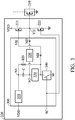
- Fig. 3 is a schematic diagram of the charge pump in the power circuit 200 of Fig. 2 in accordance with the invention.
- the charge pump 300 which is coupled to the driving node ND and the high-side node NH, includes a first unidirectional conducting device 310, a discharge resistor RD, a capacitor C, a second unidirectional conducting device 320, a third unidirectional conducting device 330, and a switch 340.
- the first unidirectional conducting device 310 When the supply voltage VDD exceeds the voltage of the first node N1, the first unidirectional conducting device 310 is turned ON. When the voltage VDD does not exceed the voltage of the first node N1, the first unidirectional conducting device 310 is turned OFF.
- the capacitor C is coupled between the first node N1 and the second node N2.
- the discharge resistor RD is coupled between the first node N1 and the high-side node NH
- the second unidirectional conducting device 320 is coupled between the second node N2 and the high-side node NH. When the voltage of the second node N2 exceeds the high-side voltage VH, the second unidirectional conducting device 320 is turned ON. When the voltage of the second node N2 does not exceed the high-side voltage VH, the second unidirectional conducting device 320 is turned OFF.
- the third unidirectional conducting device 330 is coupled between the driving node ND and the second node N2.
- the third unidirectional conducting device 330 is turned ON.
- the driving voltage VD does not exceed the voltage of the second node N2
- the third unidirectional conducting device 330 is turned OFF.
- the switch 340 receives the control signal SC and is coupled between the high-side node NH and the ground. In addition, the switch 340 is configured to couple the high-side node NH to the ground according to the control signal SC.
- the switch 340 is illustrated herein as an N-type transistor. According to an embodiment of the invention, when the control signal SC is at the high voltage level, such as the supply voltage VDD, the switch 340 is turned ON and the capacitor C is charged by the supply voltage VDD through the first unidirectional conducting device 310, the second unidirectional conducting device 320, and the switch 340 to the ground.
- the control signal SC is at the high voltage level, such as the supply voltage VDD
- the switch 340 is turned ON and the capacitor C is charged by the supply voltage VDD through the first unidirectional conducting device 310, the second unidirectional conducting device 320, and the switch 340 to the ground.
- the switch 340 when the control signal SC is at the low voltage level, such as the ground level, the switch 340 is turned OFF and the third unidirectional conducting device 330 provides the driving voltage VD to the second node N2, so that the capacitor C is discharged to the driving node ND through the discharge resistor RD
- the resistance of the discharge resistor RD determines the maximum voltage that the capacitor C can be charged and also the maximum voltage that the high-side voltage VH can be achieved.
- each of the first unidirectional conducting device 310, the second unidirectional conducting device 320, and the third unidirectional conducting device 330 is a diode. According to another embodiment of the invention, each of the first unidirectional conducting device 310, the second unidirectional conducting device 320, and the third unidirectional conducting device 330 is a diode-connected normally-off transistor.
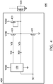
- Fig. 4 is a block diagram of a power circuit in accordance with another embodiment of the invention.
- the power circuit 400 includes a power transistor 410 and a driving circuit 420, in which the power transistor 410 and the driving circuit 420 respectively correspond to the power transistor 210 and the driving circuit 220 in Fig. 2 .
- the driving circuit 420 further includes a high-side normally-on transistor 423.
- the source terminal and the gate terminal of the high-side normally-on transistor 423 are coupled to the driving node ND, and the drain terminal of the high-side normally-on transistor 423 is supplied with the supply voltage VDD.
- the high-side normally-on transistor 423 is always turned on to improve the driving capability of the high-side transistor 221.
- Fig. 5 is a block diagram of a power circuit in accordance with yet another embodiment of the invention.
- the power circuit 500 includes a power transistor 510, a driving circuit 520, and a first pre-driver 530, in which the power transistor 510 and the driving circuit 520 respectively correspond to the power transistor 210 and the driving circuit 220 in Fig. 2 .
- the first pre-driver 530 receives the control signal SC to generate the first internal signal SI1 to the driving circuit 520 for improving the driving capability of the control signal SC.
- the first pre-driver 530 includes a first normally-on transistor 531 and a first normally-off transistor 532.
- the gate terminal and the source terminal of the first normally-on transistor 531 are coupled to the driving circuit 520, and the drain terminal of the first normally-on transistor 531 is supplied with the supply voltage VDD.
- the gate terminal of first normally-off transistor 532 receives the control signal SC, the source terminal of first normally-off transistor 532 is coupled to the ground, and the drain terminal of first normally-off transistor 532 is coupled to the driving circuit 520.
- Fig. 6 is a block diagram of a power circuit in accordance with yet another embodiment of the invention.
- the power circuit 600 includes a power transistor 610, a driving circuit 620, a first pre-driver 630, and a second pre-driver 640, in which the power transistor 610, the driving circuit 620, and the first pre-driver 630 respectively correspond to the power transistor 510, the driving circuit 520, and the first pre-driver 530 in Fig. 5 .
- the second pre-driver 640 receives the control signal SC to generate the second internal signal SI2 to the first pre-driver 630 for further improving the driving capability of the control signal SC.
- the second pre-driver 640 includes a second normally-on transistor 641 and a second normally-off transistor 642.
- the gate terminal and the source terminal of the second normally-on transistor 641 are coupled to the gate terminal of the first normally-off transistor 532 in the first pre-driver 630, and the drain terminal of the second normally-on transistor 641 is supplied with the supply voltage VDD.
- the gate terminal of the second normally-off transistor 642 receives the control signal SC, the source terminal of the second normally-off transistor 642 is coupled to the ground, and the drain terminal is coupled to the gate terminal of the first normally-off transistor 532 in the first pre-driver 630.
- Fig. 7 is a block diagram of a power circuit in accordance with yet another embodiment of the invention.
- the power circuit 700 includes a power transistor 710, a driving circuit 720, a first pre-driver 730, a second pre-driver 740, and a first hysteresis circuit 750, in which the power transistor 710, the driving circuit 720, the first pre-driver 730, and the second pre-driver 740 respectively correspond to the power transistor 610, the driving circuit 620, the first pre-driver 630, and the second pre-driver 640 in Fig. 6 .
- the first hysteresis circuit 750 receives the control signal SC to generate the third internal signal SI3 to the second pre-driver 740 for further providing a hysteresis for the control signal SC.
- the first hysteresis circuit 750 includes a first resistor R1, a third normally-off transistor 751, a fourth normally-off transistor 752, a fifth normally-off transistor 753, and a second resistor R2.
- the first resistor R1 is coupled between the supply voltage VDD and the gate terminal of the second normally-off transistor 642 in the second pre-driver 740.
- the gate terminal of the third normally-off transistor 751 is coupled to a third node N3, the source terminal of the third normally-off transistor 751 is coupled to the fourth node N4, and the drain terminal of the third normally-off transistor 751 is coupled to the first resistor R1 and the gate terminal of the second normally-off transistor 642 in the second pre-driver 740.
- the gate terminal of the fourth normally-off transistor 752 is coupled to the third node N3, the source terminal of the fourth normally-off transistor 752 is coupled to the ground, and the drain terminal of the fourth normally-off transistor 752 is coupled to the fourth node N4.
- the gate terminal of the fifth normally-off transistor 753 is coupled to the first resistor R1 and the gate terminal of the second normally-off transistor 642 in the second pre-driver 740, the source terminal of the fifth normally-off transistor 753 is coupled to the fourth node N4, and the drain terminal of the fifth normally-off transistor 753 is supplied with the supply voltage VDD.
- the second resistor R2 is coupled to the third node and receives the control signal SC.
- Fig. 8 is a block diagram of a power circuit in accordance with yet another embodiment of the invention.
- the power circuit 800 includes a power transistor 810, a driving circuit 820, a pre-driver 830, and a first hysteresis circuit 850, in which the power transistor 810, the driving circuit 820, and the first hysteresis circuit 850 respectively correspond to the power transistor 710, the driving circuit 720, and the first hysteresis circuit 750 in Fig. 7 .
- the pre-driver 830 generates the first internal signal SI1 according to the second internal signal SI2 for improving the driving capability of the control signal SC.
- the first internal signal SI1 and the second internal signal SI2 are in-phase.
- Fig. 9 is a block diagram of a power circuit in accordance with yet another embodiment of the invention.
- the power circuit 900 includes a power transistor 910, a driving circuit 920, a pre-driver 930, and a first hysteresis circuit 950, in which the power transistor 910, the driving circuit 920, the pre-driver 930, and the first hysteresis circuit 950 respectively correspond to the power transistor 810, the driving circuit 820, the pre-driver 830, and the first hysteresis circuit 850 in Fig. 8 .
- the pre-driver 930 includes a first sub pre-driver 931 and a second sub pre-driver 932.
- the first sub pre-driver 931 includes a first sub normally-off transistor E1, a second sub normally-off transistor E2, and a first sub normally-on transistor D1, in which the first sub pre-driver 931 generates the first internal signal SI1 according to a first sub-internal signal SB1.
- the gate terminal of the first sub normally-off transistor E1 receives the first sub-internal signal SB1, and the source terminal of the first sub normally-off transistor E1 is coupled to the ground.
- the gate terminal of the second sub normally-off transistor E2 receives the second internal signal SI2. Namely, the gate terminal of the second sub normally-off transistor E2 is coupled to the gate terminal of the third sub normally-on transistor E3.
- the drain terminal of the second sub normally-off transistor E2 is supplied with the supply voltage VDD.
- the source terminal of the second sub normally-off transistor E2 is coupled to the drain terminal of the first sub normally-off transistor E1, in which the drain terminal of the first sub normally-off transistor E1 generates the first internal signal SI1 to the driving circuit 920.
- the gate and source terminals of the first sub normally-on transistor D1 are coupled together.
- the drain terminal of the first sub normally-on transistor D1 is supplied with the supply voltage VDD.
- the second sub pre-driver 932 includes a third sub normally-off transistor E3, a fourth sub normally-off transistor E4, and a second sub normally-on transistor D2, in which the second sub pre-driver 932 generates the first sub-internal signal SB1 according to the second internal signal SI2.
- the gate terminal of the third sub normally-off transistor E3 receives the second internal signal SI2, and the source terminal of the third sub normally-off transistor E3 is coupled to the ground.
- the gate terminal of the fourth sub normally-off transistor E4 is coupled to the third node N3 in the first hysteresis circuit 950.
- the drain terminal of the fourth sub normally-off transistor E4 is supplied with the supply voltage VDD.
- the source terminal of the fourth sub normally-off transistor E4 is coupled to the drain terminal of the third sub normally-off transistor E3, in which the drain terminal of the third sub normally-off transistor E3 generates the first sub-internal signal SB1 to the first sub pre-driver 931.
- the gate and source terminals of the second sub normally-on transistor D2 are coupled together.
- the drain terminal of the second sub normally-on transistor D2 is supplied with the supply voltage VDD.
- Fig. 10 is a block diagram of a power circuit in accordance with yet another embodiment of the invention.
- the power circuit 1000 includes a power transistor 1010, a driving circuit 1020, a pre-driver 1030, and a first hysteresis circuit 1050, in which the power transistor 1010, the driving circuit 1020, the pre-driver 1030, and the first hysteresis circuit 1050 respectively correspond to the power transistor 910, the driving circuit 920, the pre-driver 930, and the first hysteresis circuit 950 in Fig. 9 .
- the pre-driver 1030 includes a first sub pre-driver 1031, a second sub pre-driver 1032, a third sub pre-driver 1033, and a fourth sub pre-driver 1034, in which the first sub pre-driver 1031 and the second sub pre-driver 1032 respectively correspond to the first sub pre-driver 931 and the second sub pre-driver 932 in Fig. 9 , which are not repeated herein.
- the second sub pre-driver 1032 includes a third sub normally-off transistor E3, a fourth sub normally-off transistor E4, and a second sub normally-on transistor D2, in which the second sub pre-driver 1032 generates the first sub-internal signal SB1 according to the second sub-internal signal SB2.
- the gate terminal of the third sub normally-off transistor E3 receives the second sub-internal signal SB2, and the source terminal of the third sub normally-off transistor E3 is coupled to the ground.
- the gate terminal of the fourth sub normally-off transistor E4 receives the third sub-internal signal SB3.
- the drain terminal of the fourth sub normally-off transistor E4 is supplied with the supply voltage VDD.
- the source terminal of the fourth sub normally-off transistor E4 is coupled to the drain terminal of the third sub normally-off transistor E3, in which the drain terminal of the third sub normally-off transistor E3 generates the second sub-internal signal SB2 to the first sub pre-driver 1031.
- the gate terminal and the source terminal of the second sub normally-on transistor D2 are coupled together.
- the drain terminal of the second sub normally-on transistor D2 is supplied with the supply voltage VDD.
- the third sub pre-driver 1033 includes a fifth sub normally-off transistor E5, a sixth sub normally-off transistor E6, and a third sub normally-on transistor D3, in which the third sub pre-driver 1033 generates the second sub-internal signal SB2 according to the third sub-internal signal SB3.
- the gate terminal of the fifth sub normally-off transistor E5 receives the third sub-internal signal SB3, and the source terminal of the fifth sub normally-off transistor E5 is coupled to the ground.
- the gate terminal of the sixth sub normally-off transistor E6 receives the second internal signal SI2.
- the drain terminal of the sixth sub normally-off transistor E6 is supplied with the supply voltage VDD.
- the source terminal of the sixth sub normally-off transistor E6 is coupled to the drain terminal of the fifth sub normally-off transistor E5, in which the drain terminal of the fifth sub normally-off transistor E5 generates the second sub-internal signal SB2 to the second sub pre-driver 1032.
- the gate and source terminals of the third sub normally-on transistor D3 are coupled together.
- the drain terminal of the third sub normally-on transistor D3 is supplied with the supply voltage VDD.
- the fourth sub pre-driver 1034 includes a seventh sub normally-off transistor E7, an eighth sub normally-off transistor E8, and a fourth sub normally-on transistor D4, in which the fourth sub pre-driver 1034 generates the third sub-internal signal SB3 according to the second internal signal SI2.
- the gate terminal of the seventh sub normally-off transistor E7 receives the second internal signal SI2, the source terminal of the seventh sub normally-off transistor E7 is coupled to the ground.
- the gate terminal of the eighth sub normally-off transistor E8 is coupled to the third node N3 in the first hysteresis circuit 1050.
- the drain terminal of the eighth sub normally-off transistor E8 is supplied with the supply voltage VDD.
- the source terminal of the eighth sub normally-off transistor E8 is coupled to the drain terminal of the seventh sub normally-off transistor E7, in which the drain terminal of the seventh sub normally-off transistor E7 generates the third sub-internal signal SB3 to the third sub pre-driver 1033.
- the gate and source terminals of the fourth sub normally-on transistor D4 are coupled together.
- the drain terminal of the fourth sub normally-on transistor D4 is supplied with the supply voltage VDD.
- the pre-driver 830 in Fig. 8 may include an even number of the sub pre-drivers such that the first internal signal SI1 and the second internal signal SI2 are in-phase.
- Fig. 11 is a block diagram of an integrated circuit in accordance with an embodiment of the invention.
- the integrated circuit 1100 includes a isolator 1110, a first power circuit 1120, a second power circuit 1130, a bootstrap diode DB, and a bootstrap capacitor CB.
- the isolator 1110 generates a first control signal SC1 and a second control signal SC2 according to an input signal SIN.
- the input signal SIN may be generated externally.
- a reverse input signal SINB is generated by the inverter INV.
- the isolator 1110 generates the first control signal SC1 based on the reverse input signal SINB and generates the second control signal SC2 based on the input signal SIN.
- the reverse input signal SINB and the input signal SIN may be generated externally.
- the first power circuit 1120 includes a first driving circuit 1121 and a first power transistor 1122
- the second power circuit 1130 includes a second driving circuit 1131 and a second power transistor 1132.
- the first driving circuit 1121 is identical to the second driving circuit 1131
- the first power transistor 1122 is identical to the second power transistor 1132.
- each of the first driving circuit 1121 and the second driving circuit 1131 may correspond to either one of the driving circuit 220 in Figs. 2 and 3 , the driving circuit 420 in Fig. 4 , a combination of the driving circuit 520 and the first pre-driver 530 in Fig. 5 , a combination of the driving circuit 620, the first pre-driver 630, and the second pre-driver 640 in Fig. 6 , a combination of the driving circuit 720, the first pre-driver 730, the second pre-driver 740, and the first hysteresis circuit 750 in Fig.
- each of the first power transistor 1122 and the second power transistor 1132 may correspond to either one of the power transistor 210 in Fig. 2 , the power transistor 410 in Fig. 4 , the power transistor 510 in Fig. 5 , the power transistor 610 in Fig. 6 , the power transistor 710 in Fig. 7 , the power transistor 810 in Fig. 8 , the power transistor 910 in Fig. 9 , and the power transistor 1010 in Fig. 10 .
- the bootstrap diode DB includes a bootstrap anode NBA and a bootstrap cathode NBC, in which the bootstrap anode NBA is coupled to the first supply voltage VDD1 and the bootstrap cathode NBC is coupled to the second supply voltage VDD2.
- the bootstrap capacitor CB is coupled between the second supply voltage VDD2 and a switch node NSW.
- the bootstrap diode DB and the bootstrap capacitor CB are configured to boost the first supply voltage VDD1 into the second supply voltage VDD2 based on the switch voltage VSW of the switch node NSW.
- the first driving circuit 1121 is supplied by the second supply voltage VDD2 and the switch voltage VSW, and generates the first driving voltage VD1 according to the first control signal SC1.
- the first power transistor 1122 provides the high voltage VHV to the switch node NSW according to the first driving node VD1.
- the second driving circuit 1131 is supplied by the first supply voltage VDD1 and a first ground GND1, and generates the second driving voltage VD2 according to the second control signal SC2.
- the second power transistor 1132 couples the switch node NSW to the first ground GND1 according to the second driving voltage VD2.
- the switch voltage VSW is coupled to the first ground GND1 and the second supply voltage VDD2 is equal to the first supply voltage VDD1 minus a forward voltage of the bootstrap diode DB.
- the switch voltage VSW is equal to the high voltage VHV such that the second supply voltage VDD2 is boosted into a voltage of the sum of the high voltage VHV and the first supply voltage VDD1 in order to fully turn ON the first power transistor 1122.
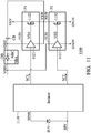
- Fig. 12 is a block diagram of an integrated circuit in accordance with another embodiment of the invention.
- the integrated circuit 1200 includes a isolator 1110, a first power circuit 1120, a second power circuit 1130, a bootstrap diode DB, and a bootstrap capacitor CB, in which the isolator 1110 includes a transmitter TX, a first receiver R1, a first isolation barrier IB1, a second receiver R2, and a second barrier IB2.
- the transmitter TX which is supplied by a third supply voltage VDD3 and a second ground GND2, modulates the input signal SIN to generate a first radio signal RF1 across the first isolation barrier IB1, and modulates the reverse input signal SINB to generate a second radio signal RF2 across the second isolation barrier IB2.
- the first receiver R1 which is supplied by the second supply voltage VDD2 and the switch voltage VSW, demodulates the first radio signal RF1 to generate the first control signal SC1.
- the first isolation barrier IB1 is configured to electrically isolate the transmitter TX from the first receiver R1.
- the second receiver R2 which is supplied by the first supply voltage VDD1 and the first ground GND1, demodulates the second radio signal RF2 to generate the second control signal SC2.
- the second isolation barrier IB2 is configured to electrically isolate the transmitter TX from the second receiver R2.
- the first ground GND1 may be identical to the second ground GND2. According to another embodiment of the invention, the first ground GND1 may not be identical to the second ground GND2. According to an embodiment of the invention, the high voltage VHV exceeds the first supply voltage VDD1, the second supply voltage VDD2, and the third supply voltage VDD3.
- the first supply voltage VDD1 may be identical to the third supply voltage VDD3. According to another embodiment of the invention, the first supply voltage VDD1 may not be identical to the third supply voltage VDD3.
- the integrated circuit 1200 further includes a decoupling capacitor CD.
- the decoupling capacitor CD is coupled between the high voltage VHV and the first ground GND1.
- the isolator 1110, the first power circuit 1120, the second power circuit 1130, and the decoupling capacitor CD are packaged together.
- the isolator 1110, the first power circuit 1120, the second power circuit 1130, the bootstrap capacitor CB, and the decoupling capacitor CD are packaged together.
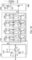
- Fig. 13 is a block diagram of an integrated circuit in accordance with another embodiment of the invention.
- the integrated circuit 1300 includes a isolator 1110, a first power circuit 1120, a second power circuit 1130, a bootstrap diode DB, and a bootstrap capacitor CB, in which the isolator 1110 includes a first sub-isolator 1111 and a second sub-isolator 1112.
- the first sub-isolator 1111 includes a first transmitter T1, a first receiver R1, and a first isolation barrier IB1.
- the first transmitter T1 which is supplied by a third supply voltage VDD3 and a second ground GND2, modulates the input signal SIN to generate a first radio signal RF1 across the first isolation barrier IB1.
- the first receiver R1 which is supplied by the second supply voltage VDD2 and the switch voltage VSW, demodulates the first radio signal RF1 to generate the first control signal SC1.
- the first isolation barrier IB1 is configured to electrically isolate the first transmitter T1 from the first receiver R1.
- the second sub-isolator 1112 includes a second transmitter T2, a second receiver R2, and a second barrier IB2.
- the second transmitter T2 which is supplied by the third supply voltage VDD3 and a second ground GND2, modulates the reverse input signal SINB to generate a second radio signal RF2 across the second isolation barrier IB2.
- the second receiver R2 which is supplied by the first supply voltage VDD1 and the first ground GND1, demodulates the second radio signal RF2 to generate the second control signal SC2.
- the second isolation barrier IB2 is configured to electrically isolate the second transmitter T2 from the second receiver R2.
- the first ground GND1 may be identical to the second ground GND2. According to another embodiment of the invention, the first ground GND1 may not be identical to the second ground GND2. According to an embodiment of the invention, the high voltage VHV exceeds the first supply voltage VDD1, the second supply voltage VDD2, and the third supply voltage VDD3.
- the first supply voltage VDD1 may be identical to the third supply voltage VDD3. According to another embodiment of the invention, the first supply voltage VDD1 may not be identical to the third supply voltage VDD3.
- the integrated circuit 1300 further includes a decoupling capacitor CD.
- the decoupling capacitor CD is coupled between the high voltage VHV and the first ground GND1.
- the first sub-isolator 1111, the second sub-isolator 1112, the first power circuit 1120, the second power circuit 1130, and the decoupling capacitor CD are packaged together.
- the first sub-isolator 1111, the second sub-isolator 1112, the first power circuit 1120, the second power circuit 1130, the bootstrap capacitor CB, and the decoupling capacitor CD are packaged together.
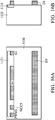
- Fig. 14 shows a top view of a package structure in accordance with an embodiment of the invention.
- the package structure 1400 includes the decoupling capacitor CD, the bootstrap capacitor CB, the first sub-isolator 1111, the second sub-isolator 1112, the first power circuit 1120, and the second power circuit 1130, which are shown in Fig. 13 .
- the package structure 1400 is deposited on a substrate 14.
- the package structure 1400 further includes a first conductive layer 1401, a second conductive layer 1402, and a third conductive layer 1403.
- the first conductive layer 1401, the second conductive layer 1402, and the third conductive layer 1403 are formed on the substrate 14.
- the first power circuit 1120 and the bootstrap capacitor CB are deposited on the first conductive layer 1401.
- the second power circuit 1130 and the decoupling capacitor CD are deposited on the second conductive layer 1402.
- the first sub-isolator 1111 and the second sub-isolator 1112 are deposited on the third conductive layer 1403.
- the first conductive layer 1401, the second conductive layer 1402, and the third conductive layer 1403 are electrically isolated from one another.
- the first conductive layer 1401 is electrically coupled to the first ground GND1
- the second conductive layer 1402 is electrically coupled to the switch voltage VSW which is coupled to the fifth reference terminal NR5.
- the fifth reference terminal NR5 which is coupled to the source terminal S1 of the first power transistor 1122, is electrically coupled to the first conductive layer 1401 through a wiring layer and a first conductor 1411.
- the first conductor 1411 is configured to electrically couple the wiring layer to the first conductive layer 1401.
- the sixth reference terminal NR6 which is coupled to the source terminal S2 of the second power transistor 1132, is electrically coupled to the second conductive layer 1402 through the wiring layer and a second conductor 1412.
- the second conductor 1412 is configured to electrically couple the wiring layer to the second conductive layer 1402.
- the bootstrap diode DB shown in Fig. 13 is placed outside of the package structure 1400.
- Fig. 15 shows a cross view of a package structure in accordance with an embodiment of the invention.
- the package structure 1500 shows the cross-sectional view along the line from A to A' shown in Fig. 14 .
- the package structure 1500 includes the substrate 14, the first sub-isolator 1111, the first power circuit 1120, the bootstrap capacitor CB, the decoupling capacitor CD, and a wiring layer 1521.
- the substrate 14 includes a first carrier 141, a second carrier 142, and a third carrier 143, in which the first carrier 141, the second carrier 142, and the third carrier 143 are insulated from one another.
- the first power circuit 1120 and the bootstrap capacitor CB are deposited on the first carrier 141.
- the decoupling capacitor CD and the second power circuit 1130 are deposited on the second carrier 142.
- the first sub-isolator 1111 and the second sub-isolator 1112 are deposited on the third carrier 143.
- the first conductive element 1522 and the first power circuit 1120 are deposited on the first conductive layer 1401, which is deposited on the first carrier 141.
- the decoupling capacitor CD and the second power circuit 1130 are deposited on the second conductive layer 1402, which is deposited on the second carrier 142.
- the first sub-isolator 1111 and the second sub-isolator 1112 are deposited on the third conductive layer 1403, which is deposited on the third carrier 143.
- the material of the first carrier 141, the second carrier 142, and the third carrier 143 may be or include stainless steel, copper (Cu), aluminum (Al), golden (Au), silver (Ag), tin (Sn), platinum (Pt), an alloy thereof, or the like.
- the first carrier 141 and the first conductive layer 1401 may be the same or different materials.
- the second carrier 142 and the second conductive layer 1402 may be the same or different materials.
- the third carrier 143 and the third conductive layer 1403 may be the same or different materials.
- the package structure 1500 further includes a first dielectric layer 1510 and a second dielectric layer 1520.
- the first sub-isolator 1111, the second sub-isolator 1112 (not shown in Fig. 15 ), the first power circuit 1120, the second power circuit 1130 (not shown in Fig. 15 ), the bootstrap capacitor CB, and the decoupling capacitor CF are bonded together in the first dielectric layer 1510.
- the wiring layer 1521 is provided on the first dielectric layer 1510 through the second dielectric layer 1520.
- the first dielectric layer 1510 is formed by a molding process through a first dielectric medium so as to bond the first sub-isolator 1111, the second sub-isolator 1112, the first power circuit 1120, and the second power circuit 1130.
- the wiring layer 1521 is configured to electrically couple the first sub-isolator 1111, the second sub-isolator 1112, the first power circuit 1120, and the second power circuit 1130.
- the material of the wiring layer 1521 is metal and is made by laser drill and metal plating process. The details of the production method will be detailed later.
- the bootstrap capacitor CB includes a first conductive element 1522, a first dielectric element 1523 and a second conductive element 1524.
- the first conductive element 1522 and the second conductive element 1524 can be a copper pillar.
- the first conductive element 1522 is provided in the first dielectric layer 1510.
- the decoupling capacitor CD includes a third conductive element 1525, a second dielectric element 1526, and a fourth conductive element 1527.
- the third conductive element 1525 and the fourth conductive element 1527 can be a copper pillar.
- the third conductive element 1525 is provided in the first dielectric layer 1510.
- the first dielectric element 1523 and the second dielectric element 1526 are provided on the first conductive element 1522.
- the second conductive element 1524 and the fourth conductive element 1527 are provided on the first dielectric element 1523.
- the first conductive element 1522, the first dielectric element 1523 and the second conductive element 1524 form the bootstrap capacitor CB.
- the third conductive element 1525, the second dielectric element 1526, and the fourth conductive element 1527 form the decoupling capacitor CD.
- the material of the first dielectric element 1523 may be different from the material of the first dielectric layer 1510 and the material of the second dielectric layer 1520.
- the material of the first dielectric element 1523 can be ceramic or mica, which is different from the material of the first dielectric medium.
- the bootstrap capacitor CB does not include the first dielectric element 1523.
- the first conductive element 1522 is spaced apart from the second conductive element 1524 by a first distance.
- the first dielectric medium of the first dielectric layer 1510 can fill the space between the first conductive element 1522 and the second conductive element 1524.
- the material of the first dielectric element 1523 may be the same as the material of the first dielectric layer 1510.
- the material of the second dielectric element 1526 may be different from the material of the first dielectric layer 1510 and the material of the second dielectric layer 1520.
- the material of the second dielectric element 1526 can be ceramic or mica, which is different from the material of the first dielectric medium.
- the decoupling capacitor CD does not include the second dielectric element 1525.
- the third conductive element 1525 is spaced apart from the fourth conductive element 1527 by a second distance.
- the first dielectric medium of the first dielectric layer 1510 can fill the space between the third conductive element 1525 and the fourth conductive element 1527.
- the material of the second dielectric element 1526 may be the same as the material of the first dielectric layer 1510.
- the first distance of the bootstrap capacitor CB may or may not be equal to the second distance of the decoupling capacitor CD.
- the first conductive element 1522 and the first dielectric element 1523 are deposited in the first dielectric layer 1510.
- the second conductive element 1524 is deposited in the second dielectric layer 1520.
- the second conductive element 1524 and the wiring layer 1521 are bonded through the second dielectric layer 1520, and the second conductive element 1524 is electrically coupled to the first power circuit 1120 through the wiring layer 1521.
- the first conductive element 1522, the first dielectric element 1523 and the second conductive element 1524 may be all deposited in the first dielectric layer 1510 and bonded through the first dielectric medium of the first dielectric layer 1510.
- the second conductive element 1524 is still electrically coupled to the first power circuit 1120 through the wiring layer 1521. The details of the production method will be detailed later.
- the third conductive element 1525 and the second dielectric element 1526 are deposited in the first dielectric layer 1510.
- the fourth conductive element 1527 is deposited in the second dielectric layer 1520.
- the fourth conductive element 1527 and the wiring layer 1521 are bonded through the second dielectric layer 1520, and the fourth conductive element 1527 is electrically coupled to the first power circuit 1120 through the wiring layer 1521.
- the third conductive element 1525, the second dielectric element 1526 and the fourth conductive element 1527 may be all deposited in the first dielectric layer 1510 and bonded through the first dielectric medium of the first dielectric layer 1510.
- the fourth conductive element 1527 is still electrically coupled to the first power circuit 1120 through the wiring layer 1521. The details of the production method will be detailed later.
- Figs. 16A-16E show a top view and a cross-sectional view of the first power circuit in accordance with an embodiment of the invention.
- Fig. 16A shows the top view of the first power circuit 1120.
- the source terminal S1, the gate terminal G1 and the drain terminal D1 of the first power transistor 1122 are illustrated respectively.
- the first driving circuit 1121 is deposited below the source terminal S1 and the gate terminal G1 of the first power transistor 1122.
- Fig. 16B shows a cross-sectional view of the first power circuit 1120. As shown in Fig. 16B , the first power transistor 1122 is deposited below the first driving circuit 1121 and the drain terminal D1 of the first power transistor 1122.
- the first conductor 1411 in Fig. 14 may be a Cu pillar.
- the first conductor 1411 is disposed on the first carrier 141 through the first conductive layer 1401 so as to electrically couple to a first side (e.g., bottom surface) of the bootstrap capacitor CB.
- the wiring layer 1521 in Fig. 15 is electrically coupled to a second side (e.g., top surface) of the bootstrap capacitor CB.
- the source terminal S1 of the first power transistor 1122 i.e., the fifth reference terminal NR5
- the source terminal S1 of the first power transistor 1122 i.e., the fifth reference terminal NR5
- the first conductor 1411 in Fig. 14 may be a Cu pillar.
- the first conductor 1411 is disposed on the first carrier 141 through the first conductive layer 1401 so as to electrically couple to a first side (e.g., bottom surface) of the bootstrap capacitor CB.
- the wiring layer 1521 in Fig. 15 is electrically coupled
- the second conductor 1412 in Fig. 14 may be a Cu pillar.
- the second conductor 1412 is disposed on the second carrier 142 through the second conductive layer 1402 so as to electrically couple to a first side (e.g., bottom surface) of the decoupling capacitor CD.
- the wiring layer 1521 in Fig. 15 is electrically coupled to a second side (e.g., top surface) of the decoupling capacitor CD.
- the source terminal S2 of the second power transistor 1132 i.e., the sixth reference terminal NR6
- the sixth reference terminal NR6 is electrically coupled to the second conductive layer 1402 through the wiring layer 1521 and the second conductor 1412.
- Figs. 17A-17F illustrate a method for fabricating the package structure 1400 of Fig. 14 and the package structure 1500 of Fig. 15 in accordance with an embodiment of the invention.
- the first conductive element 1522, the third conductive element 1525, the first sub-isolator 1111, the second sub-isolator 1112, the first power circuit 1120, the second power circuit 1130, the first conductor 1411, and the second conductor 1412 are deposited on the substrate 14.
- the first conductive element 1522 of the bootstrap capacitor CB is formed on the first carrier 141 with the first conductive layer 1401 therebetween.
- the first power circuit 1120 and the second power circuit 1130 are disposed on the first carrier 141.
- the decoupling capacitor CD is formed on the second carrier 142 with the second carrier 1402 therebetween.
- the first sub-isolator 1111 and the second sub-isolator 1112 are deposited on the third carrier 143 with the third conductive layer 1403 therebetween.
- the first dielectric element 1523 and the second dielectric element 1526 are then formed on the first conductive element 1522 and the third conductive element 1525 respectively.
- the first conductive element 1522, the first dielectric element 1523, the third conductive element 1525, the second dielectric element 1526, the first sub-isolator 1111, the second sub-isolator 1112, the first power circuit 1120, and the second power circuit 1130 are bonded together through the first dielectric medium to form the first dielectric layer 1510.
- the material of the first dielectric medium may be Epoxy or Bismaleimide Triazine Resin.
- the first molding layer 1520a on the first dielectric layer 1510 is formed by a molding process.
- multiple first metal units 1521a are formed by the laser drill and metal plating process.
- Fig. 17C and Fig. 5D after forming the first molding layer 1520a by the molding process, etching the first molding layer 1520a to form multiple holes H corresponding to the first dielectric element 1522, first conductor 1411, the second conductor 1412, and all the terminals of the first sub-isolator 1111, the second sub-isolator 1112, the first power circuit 1120, and the second power circuit 1130.
- first metal units 1521a becomes the second conductive element 1524
- first metal units 1521a becomes the fourth conductive element 1527.
- the first molding layer 1520a on the first dielectric layer 1510 is configured to fix the second conductive element 1524, the fourth conductive element 1527 and the first metal units 1521a.
- a second molding layer 1520b and multiple second metal units 1521b are formed and disposed on the first molding layer 1520a after the first molding layer 1520a is formed.
- the first metal units 1521a and the second metal units 1521b form the wiring layer 1521, so that the first sub-isolator 1111, the second sub-isolator 1112, the first power circuit 1120, the second power circuit 1130, the bootstrap capacitor CB, and the decoupling capacitor CD are electrically coupled as illustrated in Fig. 13 .
- the bootstrap capacitor CB and/or the decoupling capacitor CD which is already packaged as a package structure, on the substrate 14. That is, the first conductive element 1522, the first dielectric element 1523 and the second conductive element 1524 are first packaged into the bootstrap capacitor CB, and the third conductive element 1525, the second dielectric element 1526, and the fourth conductive element 1527 are first packaged into the decoupling capacitor CD. Then, the bootstrap capacitor CB and the decoupling capacitor CD are placed on the substrate 14.
- the first conductive element 1522, the first dielectric element 1523, the third conductive element 1525 and the second dielectric element 1526 are first packaged together and be disposed on the substrate 14. Then, after forming the first dielectric layer 1510 and depositing the first conductive element 1522, the first dielectric element 1523, the third conductive element 1525 and the second dielectric element 1526, the second conductive 1224 and the fourth conductive element 1527 are formed on the first dielectric layer 1510.
- the second conductive element 1524 is formed on the first dielectric element 1523 and disposed in the second dielectric layer 1520
- the fourth conductive element 1527 is formed on the second dielectric element 1526 and disposed on the second dielectric layer 1520.
- the method is disposing the second conductive element 1522 on the first dielectric element 1523 and the fourth conductive element 1527 on the second dielectric element 1526.
- first conductive element 1522, the first dielectric element 1523, the second conductive element 1524, the third conductive element 1525, the second dielectric element 1526, and the fourth conductive element 1527 are all deposed in the first dielectric layer 1510.
- the first dielectric medium fixes the first conductive element 1522, the third conductive element 1526, the first sub-isolator 1111, the second sub-isolator 1112, the first power circuit 1120, and the second power circuit 1130.
- the first dielectric medium is used for the first dielectric element 1523 and/or the second dielectric element 1526.
- the second conductive element 1524 is deposited on the first dielectric layer 1510, and the fourth conductive element 1527 is deposited on the first dielectric layer 1510.
- the first conductive element 1522 is spaced apart from the second conductive element 1524 by a first distance
- the third conductive element 1525 is spaced apart from the fourth conductive element 1527 with a second distance, in which the first distance may or may not be equal to the second distance.
- the first conductive element 1522, the second conductive element 1524 and the first dielectric medium between the first conductive element 1522 and the second conductive element 1524 form the bootstrap capacitor CB
- the third conductive element 1525, the fourth conductive element 1527 and the first dielectric medium between the third conductive element 1525 and the fourth conductive element 1527 form the decoupling capacitor CD.
- the second dielectric layer 1520 is formed once and multiple holes are also formed again. Then, the metal units 1522b are formed by the laser drill and metal plating process. Therefore, the first sub-isolator 1111, the second sub-isolator 1112, the first power circuit 1120, the second power circuit 1130, the bootstrap capacitor CB, and the decoupling capacitor CD are electrically coupled accordingly.
Landscapes
- Engineering & Computer Science (AREA)
- Power Engineering (AREA)
- Electronic Switches (AREA)
- Semiconductor Integrated Circuits (AREA)
Abstract
Description
- The disclosure relates generally to driving circuits and isolators integrated with GaN power transistors, and more specifically it relates to a package structure including the driving circuits, isolators, and GaN power transistors.
- In a power circuit, a charge pump is always required to boost the supply voltage to a higher voltage for driving the power transistor.
Fig. 1 illustrates a conventional power circuit. As shown inFig. 1 , the high-side driver DRV1 is configured to drive thefirst power transistor 110A, and the low-side driver DRV2 is configured to drive thesecond power transistor 110B. In addition, the boost capacitor CB and the boost diode DB are configured to boost the supply voltage VDD to the boost voltage VB, so that thefirst power transistor 110A can be fully turned on. Therefore, thefirst power transistor 110A supplied with the input voltage VIN and thesecond power transistor 110B can drive the load device RL through the inductor L and the capacitor C. - Since the inductor L may induce significant parasitic effects at the switch node SW (such as a negative voltage spike generated at the switch node SW by the turned-on body diode of the
second power transistor 110B), these parasitic effects can interfere with the boost voltage VB when the boost capacitor CB is charged through the power transistor. Therefore, it is necessary to eliminate parasitic effects from the driving circuit. - In an embodiment, an integrated circuit comprises a first power transistor, a second power transistor, and an isolator. The first power transistor is integrated with a first driving circuit. The second power transistor is integrated with a second driving circuit. The isolator provides a first control signal and a second control signal to the first power transistor and a second power transistor respectively, according to an input signal.
- According to an embodiment of the invention, the integrated circuit further comprises a first power circuit and a second power circuit, wherein the first power circuit comprises the first driving circuit and the first power transistor, wherein the second power circuit comprises the second driving circuit and the second power transistor.
- According to an embodiment of the invention, the integrated circuit further comprises a bootstrap diode and a bootstrap capacitor. The bootstrap diode comprises a bootstrap anode and a bootstrap cathode, wherein the bootstrap anode is coupled to a first supply voltage and the bootstrap cathode is coupled to a second supply voltage. The bootstrap capacitor is coupled between the second supply voltage and a switch voltage of a switch node.
- According to an embodiment of the invention, the first driving circuit is supplied by the second supply voltage and the switch voltage and generates a first driving voltage at a first driving node according to the first control signal. The first power transistor supplies a high voltage to the switch node according to the first driving voltage.
- According to an embodiment of the invention, the second driving circuit is supplied by the first supply voltage and a first ground and generates a second driving voltage at a second driving node according to the second control signal. The second power transistor pulls the switch voltage down to the first ground according to the second driving voltage.
- According to an embodiment of the invention, each of the first power transistor and the second power transistor is a GaN transistor.
- According to an embodiment of the invention, the high voltage exceeds the first supply voltage and the second supply voltage.
- According to an embodiment of the invention, the isolator comprises a first sub-isolator and a second sub-isolator. The first sub-isolator comprises a first transmitter, a first receiver, and a first isolation barrier. The first transmitter is supplied with a third supply voltage and a second ground and transmits a first radio signal according to the input signal. The first receiver is supplied with the second supply voltage and the switch voltage and generates the first control signal according to the first radio signal. The first isolation barrier is configured to electrically isolate the first transmitter from the first receiver. The second sub-isolator comprises a second transmitter, a second receiver, and a second isolation barrier. The second transmitter is supplied with a third supply voltage and a second ground and transmits a second radio signal according to the input signal. The second receiver is supplied with the first supply voltage and the first ground and generates the first control signal according to the first radio signal. The second isolation barrier is configured to electrically isolate the second transmitter from the second receiver.
- According to an embodiment of the invention, the isolator comprises: a transmitter, a first receiver, a first isolation barrier, a second receiver, and a second isolation barrier. The transmitter is supplied with a third supply voltage and a second ground and transmits a first radio signal and a second radio signal according to the input signal. The first receiver is supplied with the second supply voltage and the switch voltage and generates the first control signal according to the first radio signal. The first isolation barrier is configured to electrically isolate the transmitter from the first receiver. The second receiver is supplied with the first supply voltage and the first ground and generates the first control signal according to the first radio signal. The second isolation barrier is configured to electrically isolate the transmitter from the second receiver.
- According to an embodiment of the invention, the integrated circuit further comprises a decoupling capacitor. The decoupling capacitor is coupled between the high voltage and the first ground, wherein the first sub-isolator, the second sub-isolator, the first power circuit, a second power circuit, and the decoupling capacitor are packaged together.
- According to an embodiment of the invention, each of the first power circuit and the second power circuit comprises a pre-driver. The pre-driver generates a first internal signal according to the control signal, wherein the pre-driver is configured to improve driving capability of the control signal, wherein the driving circuit generates the driving voltage according to the first internal signal.
- According to an embodiment of the invention, each of the first driving circuit and the second driving circuit comprises a high-side transistor, a low-side transistor, and a charge pump. The high-side transistor provides a supply voltage to a driving node according to a high-side voltage of a high-side node. The low-side transistor couples the driving node to the ground according to a first internal signal. The charge pump is coupled to the high-side node and the driving node, wherein the charge pump is configured to generate a high-side voltage that exceeds the supply voltage according to the first internal signal.
- According to an embodiment of the invention, each of the first power circuit and the second power circuit comprises a hysteresis circuit. The hysteresis circuit is coupled between the control signal and the pre-driver, wherein the hysteresis circuit receives the control signal to generate a second internal signal, such that the pre-driver generates the first internal signal according to the second internal signal, wherein the hysteresis circuit is configured to provide a hysteresis for the control signal.
- According to an embodiment of the invention, the hysteresis circuit comprises a first resistor, a third normally-off transistor, a fourth normally-off transistor, a fifth normally-off transistor, and a second resistor. The first resistor is coupled between the supply voltage and an output node, wherein the second internal signal is generated at the output node. The third normally-off transistor comprises a gate terminal coupled to a third node, a source terminal coupled to a fourth node, and a drain terminal coupled to the output node. The fourth normally-off transistor comprises a gate terminal coupled to the third node, a source terminal coupled to the ground, and a drain terminal coupled to the fourth node. The fifth normally-off transistor comprises a gate terminal coupled to the output node, a source terminal coupled to the fourth node, and a drain terminal supplied by the supply voltage. The second resistor is coupled to the third node and receives the control signal.
- According to an embodiment of the invention, the pre-driver comprises a first sub pre-driver, a second sub pre-driver, a third sub pre-driver, and a fourth sub pre-driver. The first sub pre-driver generates the first internal signal according to a first sub-internal signal. The second sub pre-driver generates the first sub-internal signal according to a second sub-internal signal. The third sub pre-driver generates the second sub-internal signal according to a third internal signal. The fourth sub pre-driver generates the third sub-internal signal according to the second internal signal.
- According to an embodiment of the invention, the first sub pre-driver comprises: a first sub normally-off transistor, a second sub normally-off transistor, and a first sub normally-on transistor. The first sub normally-off transistor comprises a gate terminal receiving the first sub-internal signal, a source terminal coupled to the ground, and a drain terminal generating the first internal signal. The second sub normally-off transistor comprises a gate terminal receiving the second sub-internal signal, a source terminal coupled to the drain terminal of the first sub normally-off transistor, and a drain terminal supplied with the supply voltage. The first sub normally-on transistor comprises a gate terminal coupled to the drain terminal of the first sub normally-off transistor, a source terminal coupled to the drain terminal of the first sub normally-off transistor, and a drain terminal supplied with the supply voltage.
- According to an embodiment of the invention, the second sub pre-driver comprises: a third sub normally-off transistor, a fourth sub normally-off transistor, and a second sub normally-on transistor. The third sub normally-off transistor comprises a gate terminal receiving the second sub-internal signal, a source terminal coupled to the ground, and a drain terminal generating the first sub-internal signal. The fourth sub normally-off transistor comprises a gate terminal receiving the third sub-internal signal, a source terminal coupled to the drain terminal of the third sub normally-off transistor, and a drain terminal supplied with the supply voltage. The second sub normally-on transistor comprises a gate terminal coupled to the drain terminal of the third sub normally-off transistor, a source terminal coupled to the drain terminal of the third sub normally-off transistor, and a drain terminal supplied with the supply voltage.
- According to an embodiment of the invention, the third sub pre-driver comprises: a fifth sub normally-off transistor, a sixth sub normally-off transistor, and a third sub normally-on transistor. The fifth sub normally-off transistor comprises a gate terminal receiving the third sub-internal signal, a source terminal coupled to the ground, and a drain terminal generating the second sub-internal signal. The sixth sub normally-off transistor comprises a gate terminal receiving the second internal signal, a source terminal coupled to the drain terminal of the fifth sub normally-off transistor, and a drain terminal supplied with the supply voltage. The third sub normally-on transistor comprises a gate terminal coupled to the drain terminal of the fifth sub normally-off transistor, a source terminal coupled to the drain terminal of the fifth sub normally-off transistor, and a drain terminal supplied with the supply voltage.
- According to an embodiment of the invention, the fourth sub pre-driver comprises: a seventh sub normally-off transistor, an eighth sub normally-off transistor, and a fourth sub normally-on transistor. The seventh sub normally-off transistor comprises a gate terminal receiving the second internal signal, a source terminal coupled to the ground, and a drain terminal generating the third sub-internal signal. The eighth sub normally-off transistor comprises a gate terminal coupled to the third node of the first hysteresis circuit, a source terminal coupled to the drain terminal of the seventh sub normally-off transistor, and a drain terminal supplied with the supply voltage. The fourth sub normally-on transistor comprises a gate terminal coupled to the drain terminal of the seventh sub normally-off transistor, a source terminal coupled to the drain terminal of the seventh sub normally-off transistor, and a drain terminal supplied with the supply voltage.
- According to an embodiment of the invention, the high-side transistor and the low-side transistor are normally-off transistors.
- According to an embodiment of the invention, the charge pump comprises: a first unidirectional conducting device, a capacitor, a discharge resistor, a second unidirectional conducting device, a third unidirectional conducting device, and a switch. The first unidirectional conducting device unidirectionally provides the supply voltage to a first node. The capacitor is coupled between the first node and a second node. The discharge resistor is coupled between the first node and the high-side node. The second unidirectional conducting device unidirectionally couples the second node to the high-side node when a voltage of the second node exceeds a voltage of the high-side node. The third unidirectional conducting device unidirectionally provides the driving voltage to the second node when the driving voltage exceeds the voltage of the second node. The switch receives the control signal and is configured to couple the high-side node to the ground according to the control signal.
- According to an embodiment of the invention, when the control signal is at a high voltage level, the switch is turned ON and the capacitor is charged by the supply voltage through the first unidirectional conducting device, the second unidirectional conducting device, and the switch. When the control signal is at a low voltage level, the switch is turned OFF, the third unidirectional conducting device provides the driving voltage to the second node, and the capacitor is discharged to the high-side node through the discharge resistor.
- According to an embodiment of the invention, each of the first unidirectional conducting device, the second unidirectional conducting device, and the third unidirectional conducting device is a diode or a diode-connected normally-off transistor.
- According to an embodiment of the invention, each of the first driving circuit and the second driving circuit further comprises: a high-side normally-on transistor. The high-side normally-on transistor comprises a source terminal coupled to the driving node, a gate terminal coupled to the driving node, and a drain terminal supplied with the supply voltage, wherein the high-side normally-on transistor is configured to improve driving capability of the high-side transistor.
- In an embodiment, a package structure comprises a substrate, a decoupling capacitor, an integrated circuit, and a wiring layer. The decoupling capacitor is provided on the substrate. The integrated circuit is bonded to the decoupling capacitor in a first dielectric layer. The wiring layer is configured to electrically couple the decoupling capacitor to the integrated circuit, wherein the wiring layer is provided on the first dielectric layer through a second dielectric layer.
- According to an embodiment of the invention, the decoupling capacitor comprises: a first conductive element, a first dielectric element, and a second conductive element. The first conductive element is formed in the first dielectric layer. The first dielectric element is formed on the first conductive element. The second conductive element is formed on the first dielectric element.
- According to an embodiment of the invention, the package structure further comprises a bootstrap capacitor. The bootstrap capacitor is provided on the substrate, wherein the integrated circuit is bonded to the bootstrap capacitor in the first dielectric layer.
- According to an embodiment of the invention, the bootstrap capacitor comprises: a third conductive element, a second dielectric element, and a fourth conductive element. The third conductive element is formed in the first dielectric layer. The second dielectric element is formed on the first conductive element. The fourth conductive element is formed on the second dielectric element.
- According to an embodiment of the invention, a material of the first dielectric element and the second dielectric element is different than a material of the first dielectric layer and a material of the second dielectric layer.
- According to an embodiment of the invention, the integrated circuit comprises: an isolator, a first power circuit, and a second power circuit. The isolator generates a first control signal a second control signal according to an input signal. The first power circuit comprises: a first driving circuit and a first power transistor. The first driving circuit is supplied by a second supply voltage and a switch voltage and generates a first driving voltage at a first driving node according to the first control signal, wherein a bootstrap diode and the bootstrap capacitor are configured to boost a first supply voltage into the second supply voltage, wherein the bootstrap diode comprises a bootstrap anode coupled to the first supply voltage and a bootstrap cathode coupled to the second supply voltage, wherein the bootstrap capacitor is coupled between the second supply voltage and the switch voltage of a switch node. The first power transistor supplies a high voltage to the switch node according to the first driving voltage. The second power circuit comprises: a second driving circuit and a second power transistor. The second driving circuit is supplied by the first supply voltage and a first ground and generates a second driving voltage at a second driving node according to the second control signal. The second power transistor pulls the switch voltage down to the first ground according to the second driving voltage.
- According to an embodiment of the invention, each of the first power transistor and the second power transistor is a GaN transistor.
- According to an embodiment of the invention, the high voltage exceeds the first supply voltage and the second supply voltage.
- According to an embodiment of the invention, the isolator comprises: a first sub-isolator and a second sub-isolator. The first sub-isolator comprises a first transmitter, a first receiver, and a first isolation barrier. The first transmitter is supplied with a third supply voltage and a second ground and transmits a first radio signal according to the input signal. The first receiver is supplied with the second supply voltage and the switch voltage and generates the first control signal according to the first radio signal. The first isolation barrier is configured to electrically isolate the first transmitter from the first receiver. The second sub-isolator comprises: a second transmitter, a second receiver, and a second isolation barrier. The second transmitter is supplied with a third supply voltage and a second ground and transmits a second radio signal according to the input signal. The second receiver is supplied with the first supply voltage and the first ground and generates the first control signal according to the first radio signal. The second isolation barrier is configured to electrically isolate the second transmitter from the second receiver.
- According to an embodiment of the invention, the isolator comprises a transmitter, a first receiver, a first isolation barrier, a second receiver, and a second isolation barrier. The transmitter is supplied with a third supply voltage and a second ground and transmitting a first radio signal and a second radio signal according to the input signal. The first receiver is supplied with the second supply voltage and the switch voltage and generating the first control signal according to the first radio signal. The first isolation barrier is configured to electrically isolate the transmitter from the first receiver. The second receiver is supplied with the first supply voltage and the first ground and generates the first control signal according to the first radio signal. The second isolation barrier, configured to electrically isolate the transmitter from the second receiver.
- According to an embodiment of the invention, the decoupling capacitor is coupled between the high voltage and the first ground.
- According to an embodiment of the invention, each of the first power circuit and the second power circuit comprises: a pre-driver. The pre-driver generates a first internal signal according to the control signal, wherein the pre-driver is configured to improve driving capability of the control signal, wherein the driving circuit generates the driving voltage according to the first internal signal.
- According to an embodiment of the invention, each of the first driving circuit and the second driving circuit comprises: a high-side transistor, a low-side transistor, and a charge pump. The high-side transistor provides a supply voltage to a driving node according to a high-side voltage of a high-side node. The low-side transistor couples the driving node to the ground according to a first internal signal. The charge pump is coupled to the high-side node and the driving node, wherein the charge pump is configured to generate a high-side voltage that exceeds the supply voltage according to the first internal signal.
- According to an embodiment of the invention, each of the first power circuit and the second power circuit comprises: a hysteresis circuit. The hysteresis circuit is coupled between the control signal and the pre-driver, wherein the hysteresis circuit receives the control signal to generate a second internal signal, such that the pre-driver generates the first internal signal according to the second internal signal, wherein the hysteresis circuit is configured to provide a hysteresis for the control signal.
- According to an embodiment of the invention, each of the first driving circuit and the second driving circuit further comprises a high-side normally-on transistor. The high-side normally-on transistor comprises a source terminal coupled to the driving node, a gate terminal coupled to the driving node, and a drain terminal supplied with the supply voltage, wherein the high-side normally-on transistor is configured to improve driving capability of the high-side transistor.
- According to an embodiment of the invention, the high-side transistor and the low-side transistor are normally-off transistors.
- According to an embodiment of the invention, the charge pump comprises: a first unidirectional conducting device, a capacitor, a discharge resistor, a second unidirectional conducting device, a third unidirectional conducting device, and a switch. The first unidirectional conducting device unidirectionally provides the supply voltage to a first node. The capacitor is coupled between the first node and a second node. The discharge resistor is coupled between the first node and the high-side node. The second unidirectional conducting device unidirectionally couples the second node to the high-side node when a voltage of the second node exceeds a voltage of the high-side node. The third unidirectional conducting device unidirectionally provides the driving voltage to the second node when the driving voltage exceeds the voltage of the second node. The switch receives the control signal and configured to couple the high-side node to the ground according to the control signal.
- According to an embodiment of the invention, when the control signal is at a high voltage level, the switch is turned ON and the capacitor is charged by the supply voltage through the first unidirectional conducting device, the second unidirectional conducting device, and the switch, wherein, when the control signal is at a low voltage level, the switch is turned OFF, the third unidirectional conducting device provides the driving voltage to the second node, and the capacitor is discharged to the high-side node through the discharge resistor.
- According to an embodiment of the invention, each of the first unidirectional conducting device, the second unidirectional conducting device, and the third unidirectional conducting device is a diode or a diode-connected normally-off transistor.
- According to an embodiment of the invention, each of the first driving circuit and the second driving circuit further comprises: a high-side normally-on transistor. The high-side normally-on transistor comprises a source terminal coupled to the driving node, a gate terminal coupled to the driving node, and a drain terminal supplied with the supply voltage, wherein the high-side normally-on transistor is configured to improve driving capability of the high-side transistor.
- In an embodiment, a method of fabricating a package structure comprises: providing a decoupling capacitor on a substrate; providing an integrated circuit on the substrate; bonding the decoupling capacitor and the integrated circuit through a first dielectric medium to form a first dielectric layer; forming a wiring layer on the first dielectric layer, so that the decoupling capacitor is electrically coupled to the integrated circuit through the wiring layer; and bonding the wiring layer to the first dielectric layer through a second dielectric medium to form a second dielectric layer on the first dielectric layer.
- According to an embodiment of the invention, the step of providing the decoupling capacitor on the substrate further comprising: forming a first conductive element in the first dielectric layer; forming a first dielectric element on the first conductive element; and forming a second conductive element on the first dielectric element.
- According to an embodiment of the invention, the method further comprises: providing a bootstrap capacitor on the substrate; and bonding the bootstrap capacitor, the decoupling capacitor, and the integrated circuit through the first dielectric medium to form the first dielectric layer.
- According to an embodiment of the invention, the step of providing the bootstrap capacitor on the substrate further comprises: forming a third conductive element in the first dielectric layer; forming a second dielectric element on the first conductive element; and forming a fourth conductive element on the second dielectric element.
- According to an embodiment of the invention, the integrated circuit comprises: an isolator, a first power circuit, and a second power circuit. The isolator comprises a first supply terminal, a second supply terminal, a third supply terminal, a fourth supply terminal, a first reference terminal, a second reference terminal, a third reference terminal, a fourth reference terminal, a first input terminal, a second input terminal, a first output terminal, and a second output terminal. The first power circuit comprises a fifth supply terminal coupled to the second supply terminal, a sixth supply terminal, a fifth reference terminal coupled to the second reference terminal, and a first PWM terminal coupled to the first output terminal. The second power circuit comprises a seventh supply terminal coupled to the fourth supply terminal, an eighth supply terminal coupled to the fifth reference terminal, a sixth reference terminal, and a second PWM terminal coupled to the second output terminal.
- According to an embodiment of the invention, the method further comprises: forming a first conductive layer on the substrate, wherein the first power circuit and the bootstrap capacitor are deposited on the first conductive layer, wherein the first conductive layer is coupled to a first side of the bootstrap capacitor and the fifth reference terminal, and a second side of the bootstrap capacitor is coupled to the fifth supply terminal through the wiring layer, wherein the sixth supply terminal is coupled to a third side of the decoupling capacitor through the wiring layer.
- According to an embodiment of the invention, the method further comprises: forming a second conductive layer on the substrate, wherein the second power circuit and the decoupling capacitor are deposited on the second conductive layer, wherein the second conductive layer is coupled to a fourth side of the decoupling capacitor and a sixth reference terminal.
- According to an embodiment of the invention, the method further comprises: forming a third conductive layer on the substrate, wherein the isolator is deposited on the third conductive layer.
- According to an embodiment of the invention, the first supply terminal and the third supply terminal are supplied with a third supply voltage, the second supply terminal and the fifth supply terminal are supplied with a second supply voltage, the first input terminal receives a input signal, the second input terminal receives a reverse input signal, the first output terminal generates a first control signal, the second output terminal generates a second control signal, the fourth supply terminal and the seventh supply terminal are supplied with a first supply voltage, the sixth supply terminal is supplied with a high voltage, the eighth supply terminal is coupled to the second reference terminal and the fifth reference terminal, the first reference terminal and the third reference terminal are coupled to a second ground, and the fourth reference terminal and the sixth reference terminal are coupled to a first ground, wherein the input signal and the reverse input signal are out-of-phase.
- According to an embodiment of the invention, the first power circuit comprises: a first driving circuit and a first power transistor. The first driving circuit is supplied by the second supply voltage and the switch voltage and generates a first driving voltage at a first driving node according to the first control signal. The first power transistor couples the sixth supply terminal to the fifth reference terminal according to the first driving voltage.
- According to an embodiment of the invention, the second power circuit comprises: a second driving circuit and a second power transistor. The second driving circuit is supplied by the first supply voltage and a first ground and generating a second driving voltage at a second driving node according to the second control signal. The second power transistor couples the eighth supply terminal to the first ground according to the second driving voltage.
- According to an embodiment of the invention, each of the first power transistor and the second power transistor is a GaN transistor.
- According to an embodiment of the invention, the integrated circuit further comprises: a bootstrap diode. The bootstrap diode comprises a bootstrap anode and a bootstrap cathode, wherein the bootstrap anode is coupled to a first supply voltage and the bootstrap cathode is coupled to a second supply voltage.
- According to an embodiment of the invention, the high voltage exceeds the first supply voltage and the second supply voltage.
- According to an embodiment of the invention, the isolator comprises a first sub-isolator and a second sub-isolator. The first sub-isolator comprises a first transmitter, a first receiver, and a first isolation barrier. The first transmitter is supplied with a third supply voltage and a second ground and transmits a first radio signal according to the input signal. The first receiver is supplied with the second supply voltage and the switch voltage and generates the first control signal according to the first radio signal. The first isolation barrier is configured to electrically isolate the first transmitter from the first receiver. The second sub-isolator comprises a second transmitter, a second receiver, and a second isolation barrier. The second transmitter is supplied with a third supply voltage and a second ground and transmits a second radio signal according to the input signal. The second receiver is supplied with the first supply voltage and the first ground and generates the first control signal according to the first radio signal. The second isolation barrier is configured to electrically isolate the second transmitter from the second receiver.
- According to an embodiment of the invention, each of the first power circuit and the second power circuit comprises a pre-driver. The pre-driver generates a first internal signal according to the control signal, wherein the pre-driver is configured to improve driving capability of the control signal, wherein the driving circuit generates the driving voltage according to the first internal signal.
- According to an embodiment of the invention, each of the first driving circuit and the second driving circuit comprises a high-side transistor, a low-side transistor, and a charge pump. The high-side transistor provides a supply voltage to a driving node according to a high-side voltage of a high-side node. The low-side transistor couples the driving node to the ground according to a first internal signal. The charge pump is coupled to the high-side node and the driving node, wherein the charge pump is configured to generate a high-side voltage that exceeds the supply voltage according to the first internal signal.
- According to an embodiment of the invention, each of the first power circuit and the second power circuit comprises a hysteresis circuit. The hysteresis circuit is coupled between the control signal and the pre-driver, wherein the hysteresis circuit receives the control signal to generate a second internal signal, such that the pre-driver generates the first internal signal according to the second internal signal, wherein the hysteresis circuit is configured to provide a hysteresis for the control signal.
- According to an embodiment of the invention, the hysteresis circuit comprises a first resistor, a third normally-off transistor, a fourth normally-off transistor, a fifth normally-off transistor, and a second resistor. The first resistor is coupled between the supply voltage and an output node, wherein the second internal signal is generated at the output node. The third normally-off transistor comprises a gate terminal coupled to a third node, a source terminal coupled to a fourth node, and a drain terminal coupled to the output node. The fourth normally-off transistor comprises a gate terminal coupled to the third node, a source terminal coupled to the ground, and a drain terminal coupled to the fourth node. The fifth normally-off transistor comprises a gate terminal coupled to the output node, a source terminal coupled to the fourth node, and a drain terminal supplied by the supply voltage. The second resistor is coupled to the third node and receives the control signal.
- According to an embodiment of the invention, the pre-driver comprises a first sub pre-driver, a second sub pre-driver, a third sub pre-driver, and a fourth sub pre-driver. The first sub pre-driver generates the first internal signal according to a first sub-internal signal. The second sub pre-driver generates the first sub-internal signal according to a second sub-internal signal. The third sub pre-driver generates the second sub-internal signal according to a third internal signal. The fourth sub pre-driver generates the third sub-internal signal according to the second internal signal.
- According to an embodiment of the invention, the first sub pre-driver comprises: a first sub normally-off transistor, a second sub normally-off transistor, and a first sub normally-on transistor. The first sub normally-off transistor comprises a gate terminal receiving the first sub-internal signal, a source terminal coupled to the ground, and a drain terminal generating the first internal signal. The second sub normally-off transistor comprises a gate terminal receiving the second sub-internal signal, a source terminal coupled to the drain terminal of the first sub normally-off transistor, and a drain terminal supplied with the supply voltage. The first sub normally-on transistor comprises a gate terminal coupled to the drain terminal of the first sub normally-off transistor, a source terminal coupled to the drain terminal of the first sub normally-off transistor, and a drain terminal supplied with the supply voltage.
- According to an embodiment of the invention, the second sub pre-driver comprises: a third sub normally-off transistor, a fourth sub normally-off transistor, and a second sub normally-on transistor. The third sub normally-off transistor comprises a gate terminal receiving the second sub-internal signal, a source terminal coupled to the ground, and a drain terminal generating the first sub-internal signal. The fourth sub normally-off transistor comprises a gate terminal receiving the third sub-internal signal, a source terminal coupled to the drain terminal of the third sub normally-off transistor, and a drain terminal supplied with the supply voltage. The second sub normally-on transistor comprises a gate terminal coupled to the drain terminal of the third sub normally-off transistor, a source terminal coupled to the drain terminal of the third sub normally-off transistor, and a drain terminal supplied with the supply voltage.
- According to an embodiment of the invention, the third sub pre-driver comprises: a fifth sub normally-off transistor, a sixth sub normally-off transistor, and a third sub normally-on transistor. The fifth sub normally-off transistor comprises a gate terminal receiving the third sub-internal signal, a source terminal coupled to the ground, and a drain terminal generating the second sub-internal signal. The sixth sub normally-off transistor comprises a gate terminal receiving the second internal signal, a source terminal coupled to the drain terminal of the fifth sub normally-off transistor, and a drain terminal supplied with the supply voltage. The third sub normally-on transistor comprises a gate terminal coupled to the drain terminal of the fifth sub normally-off transistor, a source terminal coupled to the drain terminal of the fifth sub normally-off transistor, and a drain terminal supplied with the supply voltage.
- According to an embodiment of the invention, the fourth sub pre-driver comprises: a seventh sub normally-off transistor, an eighth sub normally-off transistor, and a fourth sub normally-on transistor. The seventh sub normally-off transistor comprises a gate terminal receiving the second internal signal, a source terminal coupled to the ground, and a drain terminal generating the third sub-internal signal. The eighth sub normally-off transistor comprises a gate terminal coupled to the third node of the first hysteresis circuit, a source terminal coupled to the drain terminal of the seventh sub normally-off transistor, and a drain terminal supplied with the supply voltage. The fourth sub normally-on transistor comprises a gate terminal coupled to the drain terminal of the seventh sub normally-off transistor, a source terminal coupled to the drain terminal of the seventh sub normally-off transistor, and a drain terminal supplied with the supply voltage.
- According to an embodiment of the invention, the high-side transistor and the low-side transistor are normally-off transistors.
- According to an embodiment of the invention, the charge pump comprises: a first unidirectional conducting device, a capacitor, a discharge resistor, a second unidirectional conducting device, a third unidirectional conducting device, and a switch. The first unidirectional conducting device unidirectionally provides the supply voltage to a first node. The capacitor is coupled between the first node and a second node. The discharge resistor is coupled between the first node and the high-side node. The second unidirectional conducting device unidirectionally couples the second node to the high-side node when a voltage of the second node exceeds a voltage of the high-side node. The third unidirectional conducting device unidirectionally provides the driving voltage to the second node when the driving voltage exceeds the voltage of the second node. The switch receives the control signal and is configured to couple the high-side node to the ground according to the control signal.
- According to an embodiment of the invention, when the control signal is at a high voltage level, the switch is turned ON and the capacitor is charged by the supply voltage through the first unidirectional conducting device, the second unidirectional conducting device, and the switch. When the control signal is at a low voltage level, the switch is turned OFF, the third unidirectional conducting device provides the driving voltage to the second node, and the capacitor is discharged to the high-side node through the discharge resistor.
- According to an embodiment of the invention, each of the first unidirectional conducting device, the second unidirectional conducting device, and the third unidirectional conducting device is a diode or a diode-connected normally-off transistor.
- According to an embodiment of the invention, each of the first driving circuit and the second driving circuit further comprises: a high-side normally-on transistor. The high-side normally-on transistor comprises a source terminal coupled to the driving node, a gate terminal coupled to the driving node, and a drain terminal supplied with the supply voltage, wherein the high-side normally-on transistor is configured to improve driving capability of the high-side transistor.
- A detailed description is given in the following embodiments with reference to the accompanying drawings.
- The invention can be more fully understood by reading the subsequent detailed description and examples with references made to the accompanying drawings, wherein:
-
Fig. 1 illustrates a conventional power circuit; -
Fig. 2 is a block diagram of a power circuit in accordance with an embodiment of the invention; -
Fig. 3 is a schematic diagram of the charge pump in thepower circuit 200 ofFig. 2 in accordance with the invention; -
Fig. 4 is a block diagram of a power circuit in accordance with another embodiment of the invention; -
Fig. 5 is a block diagram of a power circuit in accordance with yet another embodiment of the invention; -
Fig. 6 is a block diagram of a power circuit in accordance with yet another embodiment of the invention; -
Fig. 7 is a block diagram of a power circuit in accordance with yet another embodiment of the invention; -
Fig. 8 is a block diagram of a power circuit in accordance with yet another embodiment of the invention; -
Fig. 9 is a block diagram of a power circuit in accordance with yet another embodiment of the invention; -
Fig. 10 is a block diagram of a power circuit in accordance with yet another embodiment of the invention; -
Fig. 11 is a block diagram of an integrated circuit in accordance with an embodiment of the invention; -
Fig. 12 is a block diagram of an integrated circuit in accordance with another embodiment of the invention; -
Fig. 13 is a block diagram of an integrated circuit in accordance with yet another embodiment of the invention; -
Fig. 14 shows a top view of a package structure in accordance with an embodiment of the invention; -
Fig. 15 shows a cross view of a package structure in accordance with an embodiment of the invention; -
Figs. 16A-16B show a top view and a cross-sectional view of the first power circuit in accordance with an embodiment of the invention; and -
Figs. 17A-17F illustrate processes for fabricating thepackage structure 1400 ofFig. 14 and thepackage structure 1500 ofFig. 15 in accordance with an embodiment of the invention. - This description is made for the purpose of illustrating the general principles of the invention and should not be taken in a limiting sense. In addition, the present disclosure may repeat reference numerals and/or letters in the various examples. This repetition is for the purpose of simplicity and clarity and does not in itself dictate a relationship between the various embodiments and/or configurations discussed. The scope of the invention is best determined by reference to the appended claims.
- It is understood that the following disclosure provides many different embodiments, or examples, for implementing different features of the application. Specific examples of components and arrangements are described below to simplify the present disclosure. These are, of course, merely examples and are not intended to be limiting. In addition, the present disclosure may repeat reference numerals and/or letters in the various examples. This repetition is for the purpose of simplicity and clarity and does not in itself dictate a relationship between the various embodiments and/or configurations discussed. Moreover, the formation of a feature on, connected to, and/or coupled to another feature in the present disclosure that follows may include embodiments in which the features are formed in direct contact, and may also include embodiments in which additional features may be formed interposing the features, such that the features may not be in direct contact.
-
Fig. 2 is a block diagram of a power circuit in accordance with an embodiment of the invention. As shown inFig. 2 , thepower circuit 200 includes apower transistor 210 and adriving circuit 220. Thepower transistor 210 draws the power current IP according to the driving voltage VD of the driving node ND. According to an embodiment of the invention, thepower transistor 210 is a GaN transistor. - The driving
circuit 220 includes a high-side transistor 221, a low-side transistor 222, and acharge pump 230. The high-side transistor 221 supplies the supply voltage VDD to the driving node ND according to the high-side voltage VH of the high-side node NH The low-side transistor 222 is coupled between the driving node ND and the ground, and configured to pull the driving voltage VD down to the ground according to the control signal SC. According to an embodiment of the invention, the high-side transistor 221 and the low-side transistor 222 are normally-off transistors. - The
charge pump 230 is supplied with the supply voltage VDD and the ground and coupled to the high-side node NH and the driving node ND. For the sake of fully turning on the high-side transistor 221, thecharge pump 230 is configured to generate the high-side voltage VH exceeding the supply voltage VDD, so that the gate-to-source voltage of the high-side transistor 221 at least exceeds the threshold voltage to apply the supply voltage VDD to the driving node ND. According to an embodiment of the invention, the drivingcircuit 220 is a rail-to-rail driver, so that the driving voltage VD ranges from the supply voltage VDD to the ground level. -
Fig. 3 is a schematic diagram of the charge pump in thepower circuit 200 ofFig. 2 in accordance with the invention. As shown inFig. 3 , thecharge pump 300, which is coupled to the driving node ND and the high-side node NH, includes a firstunidirectional conducting device 310, a discharge resistor RD, a capacitor C, a secondunidirectional conducting device 320, a thirdunidirectional conducting device 330, and aswitch 340. - When the supply voltage VDD exceeds the voltage of the first node N1, the first
unidirectional conducting device 310 is turned ON. When the voltage VDD does not exceed the voltage of the first node N1, the firstunidirectional conducting device 310 is turned OFF. The capacitor C is coupled between the first node N1 and the second node N2. The discharge resistor RD is coupled between the first node N1 and the high-side node NH - The second
unidirectional conducting device 320 is coupled between the second node N2 and the high-side node NH. When the voltage of the second node N2 exceeds the high-side voltage VH, the secondunidirectional conducting device 320 is turned ON. When the voltage of the second node N2 does not exceed the high-side voltage VH, the secondunidirectional conducting device 320 is turned OFF. - The third
unidirectional conducting device 330 is coupled between the driving node ND and the second node N2. When the driving voltage VD of the driving node ND exceeds the voltage of the second node N2, the thirdunidirectional conducting device 330 is turned ON. When the driving voltage VD does not exceed the voltage of the second node N2, the thirdunidirectional conducting device 330 is turned OFF. - The
switch 340 receives the control signal SC and is coupled between the high-side node NH and the ground. In addition, theswitch 340 is configured to couple the high-side node NH to the ground according to the control signal SC. - For the simplicity of illustration, the
switch 340 is illustrated herein as an N-type transistor. According to an embodiment of the invention, when the control signal SC is at the high voltage level, such as the supply voltage VDD, theswitch 340 is turned ON and the capacitor C is charged by the supply voltage VDD through the firstunidirectional conducting device 310, the secondunidirectional conducting device 320, and theswitch 340 to the ground. - According to another embodiment of the invention, when the control signal SC is at the low voltage level, such as the ground level, the
switch 340 is turned OFF and the thirdunidirectional conducting device 330 provides the driving voltage VD to the second node N2, so that the capacitor C is discharged to the driving node ND through the discharge resistor RD - According to an embodiment of the invention, the resistance of the discharge resistor RD determines the maximum voltage that the capacitor C can be charged and also the maximum voltage that the high-side voltage VH can be achieved. In addition, the larger the resistance of the discharge resistor RD is, the lower the rising speed of the high-side voltage VD could be achieved. Therefore, there is a trade-off on the resistance of the discharge resistor RD
- According to an embodiment of the invention, each of the first
unidirectional conducting device 310, the secondunidirectional conducting device 320, and the thirdunidirectional conducting device 330 is a diode. According to another embodiment of the invention, each of the firstunidirectional conducting device 310, the secondunidirectional conducting device 320, and the thirdunidirectional conducting device 330 is a diode-connected normally-off transistor. -
Fig. 4 is a block diagram of a power circuit in accordance with another embodiment of the invention. As shown inFig. 4 , thepower circuit 400 includes apower transistor 410 and adriving circuit 420, in which thepower transistor 410 and the drivingcircuit 420 respectively correspond to thepower transistor 210 and the drivingcircuit 220 inFig. 2 . - The driving
circuit 420 further includes a high-side normally-ontransistor 423. The source terminal and the gate terminal of the high-side normally-ontransistor 423 are coupled to the driving node ND, and the drain terminal of the high-side normally-ontransistor 423 is supplied with the supply voltage VDD. The high-side normally-ontransistor 423 is always turned on to improve the driving capability of the high-side transistor 221. -
Fig. 5 is a block diagram of a power circuit in accordance with yet another embodiment of the invention. As shown inFig. 5 , thepower circuit 500 includes apower transistor 510, a drivingcircuit 520, and afirst pre-driver 530, in which thepower transistor 510 and the drivingcircuit 520 respectively correspond to thepower transistor 210 and the drivingcircuit 220 inFig. 2 . - The
first pre-driver 530 receives the control signal SC to generate the first internal signal SI1 to thedriving circuit 520 for improving the driving capability of the control signal SC. Thefirst pre-driver 530 includes a first normally-ontransistor 531 and a first normally-off transistor 532. - The gate terminal and the source terminal of the first normally-on
transistor 531 are coupled to thedriving circuit 520, and the drain terminal of the first normally-ontransistor 531 is supplied with the supply voltage VDD. The gate terminal of first normally-off transistor 532 receives the control signal SC, the source terminal of first normally-off transistor 532 is coupled to the ground, and the drain terminal of first normally-off transistor 532 is coupled to thedriving circuit 520. -
Fig. 6 is a block diagram of a power circuit in accordance with yet another embodiment of the invention. As shown inFig. 6 , thepower circuit 600 includes apower transistor 610, a drivingcircuit 620, afirst pre-driver 630, and asecond pre-driver 640, in which thepower transistor 610, the drivingcircuit 620, and thefirst pre-driver 630 respectively correspond to thepower transistor 510, the drivingcircuit 520, and thefirst pre-driver 530 inFig. 5 . - The
second pre-driver 640 receives the control signal SC to generate the second internal signal SI2 to thefirst pre-driver 630 for further improving the driving capability of the control signal SC. Thesecond pre-driver 640 includes a second normally-ontransistor 641 and a second normally-off transistor 642. - The gate terminal and the source terminal of the second normally-on
transistor 641 are coupled to the gate terminal of the first normally-off transistor 532 in thefirst pre-driver 630, and the drain terminal of the second normally-ontransistor 641 is supplied with the supply voltage VDD. The gate terminal of the second normally-off transistor 642 receives the control signal SC, the source terminal of the second normally-off transistor 642 is coupled to the ground, and the drain terminal is coupled to the gate terminal of the first normally-off transistor 532 in thefirst pre-driver 630. -
Fig. 7 is a block diagram of a power circuit in accordance with yet another embodiment of the invention. As shown inFig. 7 , thepower circuit 700 includes apower transistor 710, a drivingcircuit 720, afirst pre-driver 730, asecond pre-driver 740, and afirst hysteresis circuit 750, in which thepower transistor 710, the drivingcircuit 720, thefirst pre-driver 730, and thesecond pre-driver 740 respectively correspond to thepower transistor 610, the drivingcircuit 620, thefirst pre-driver 630, and thesecond pre-driver 640 inFig. 6 . - The
first hysteresis circuit 750 receives the control signal SC to generate the third internal signal SI3 to thesecond pre-driver 740 for further providing a hysteresis for the control signal SC. Thefirst hysteresis circuit 750 includes a first resistor R1, a third normally-off transistor 751, a fourth normally-off transistor 752, a fifth normally-off transistor 753, and a second resistor R2. - The first resistor R1 is coupled between the supply voltage VDD and the gate terminal of the second normally-
off transistor 642 in thesecond pre-driver 740. The gate terminal of the third normally-off transistor 751 is coupled to a third node N3, the source terminal of the third normally-off transistor 751 is coupled to the fourth node N4, and the drain terminal of the third normally-off transistor 751 is coupled to the first resistor R1 and the gate terminal of the second normally-off transistor 642 in thesecond pre-driver 740. The gate terminal of the fourth normally-off transistor 752 is coupled to the third node N3, the source terminal of the fourth normally-off transistor 752 is coupled to the ground, and the drain terminal of the fourth normally-off transistor 752 is coupled to the fourth node N4. - The gate terminal of the fifth normally-
off transistor 753 is coupled to the first resistor R1 and the gate terminal of the second normally-off transistor 642 in thesecond pre-driver 740, the source terminal of the fifth normally-off transistor 753 is coupled to the fourth node N4, and the drain terminal of the fifth normally-off transistor 753 is supplied with the supply voltage VDD. The second resistor R2 is coupled to the third node and receives the control signal SC. -
Fig. 8 is a block diagram of a power circuit in accordance with yet another embodiment of the invention. As shown inFig. 8 , thepower circuit 800 includes apower transistor 810, a drivingcircuit 820, a pre-driver 830, and afirst hysteresis circuit 850, in which thepower transistor 810, the drivingcircuit 820, and thefirst hysteresis circuit 850 respectively correspond to thepower transistor 710, the drivingcircuit 720, and thefirst hysteresis circuit 750 inFig. 7 . - According to an embodiment of the invention, the pre-driver 830 generates the first internal signal SI1 according to the second internal signal SI2 for improving the driving capability of the control signal SC. According to an embodiment of the invention, the first internal signal SI1 and the second internal signal SI2 are in-phase.
-
Fig. 9 is a block diagram of a power circuit in accordance with yet another embodiment of the invention. As shown inFig. 9 , thepower circuit 900 includes apower transistor 910, a drivingcircuit 920, a pre-driver 930, and afirst hysteresis circuit 950, in which thepower transistor 910, the drivingcircuit 920, the pre-driver 930, and thefirst hysteresis circuit 950 respectively correspond to thepower transistor 810, the drivingcircuit 820, the pre-driver 830, and thefirst hysteresis circuit 850 inFig. 8 . - As shown in
Fig. 9 , the pre-driver 930 includes afirst sub pre-driver 931 and asecond sub pre-driver 932. Thefirst sub pre-driver 931 includes a first sub normally-off transistor E1, a second sub normally-off transistor E2, and a first sub normally-on transistor D1, in which thefirst sub pre-driver 931 generates the first internal signal SI1 according to a first sub-internal signal SB1. - The gate terminal of the first sub normally-off transistor E1 receives the first sub-internal signal SB1, and the source terminal of the first sub normally-off transistor E1 is coupled to the ground. The gate terminal of the second sub normally-off transistor E2 receives the second internal signal SI2. Namely, the gate terminal of the second sub normally-off transistor E2 is coupled to the gate terminal of the third sub normally-on transistor E3. The drain terminal of the second sub normally-off transistor E2 is supplied with the supply voltage VDD.
- The source terminal of the second sub normally-off transistor E2 is coupled to the drain terminal of the first sub normally-off transistor E1, in which the drain terminal of the first sub normally-off transistor E1 generates the first internal signal SI1 to the
driving circuit 920. The gate and source terminals of the first sub normally-on transistor D1 are coupled together. The drain terminal of the first sub normally-on transistor D1 is supplied with the supply voltage VDD. - The
second sub pre-driver 932 includes a third sub normally-off transistor E3, a fourth sub normally-off transistor E4, and a second sub normally-on transistor D2, in which thesecond sub pre-driver 932 generates the first sub-internal signal SB1 according to the second internal signal SI2. - The gate terminal of the third sub normally-off transistor E3 receives the second internal signal SI2, and the source terminal of the third sub normally-off transistor E3 is coupled to the ground. The gate terminal of the fourth sub normally-off transistor E4 is coupled to the third node N3 in the
first hysteresis circuit 950. The drain terminal of the fourth sub normally-off transistor E4 is supplied with the supply voltage VDD. - The source terminal of the fourth sub normally-off transistor E4 is coupled to the drain terminal of the third sub normally-off transistor E3, in which the drain terminal of the third sub normally-off transistor E3 generates the first sub-internal signal SB1 to the
first sub pre-driver 931. The gate and source terminals of the second sub normally-on transistor D2 are coupled together. The drain terminal of the second sub normally-on transistor D2 is supplied with the supply voltage VDD. -
Fig. 10 is a block diagram of a power circuit in accordance with yet another embodiment of the invention. As shown inFig. 10 , thepower circuit 1000 includes apower transistor 1010, adriving circuit 1020, a pre-driver 1030, and afirst hysteresis circuit 1050, in which thepower transistor 1010, thedriving circuit 1020, the pre-driver 1030, and thefirst hysteresis circuit 1050 respectively correspond to thepower transistor 910, the drivingcircuit 920, the pre-driver 930, and thefirst hysteresis circuit 950 inFig. 9 . - As shown in
Fig. 10 , the pre-driver 1030 includes afirst sub pre-driver 1031, asecond sub pre-driver 1032, athird sub pre-driver 1033, and afourth sub pre-driver 1034, in which thefirst sub pre-driver 1031 and thesecond sub pre-driver 1032 respectively correspond to thefirst sub pre-driver 931 and thesecond sub pre-driver 932 inFig. 9 , which are not repeated herein. - The
second sub pre-driver 1032 includes a third sub normally-off transistor E3, a fourth sub normally-off transistor E4, and a second sub normally-on transistor D2, in which thesecond sub pre-driver 1032 generates the first sub-internal signal SB1 according to the second sub-internal signal SB2. - The gate terminal of the third sub normally-off transistor E3 receives the second sub-internal signal SB2, and the source terminal of the third sub normally-off transistor E3 is coupled to the ground. The gate terminal of the fourth sub normally-off transistor E4 receives the third sub-internal signal SB3. The drain terminal of the fourth sub normally-off transistor E4 is supplied with the supply voltage VDD.
- The source terminal of the fourth sub normally-off transistor E4 is coupled to the drain terminal of the third sub normally-off transistor E3, in which the drain terminal of the third sub normally-off transistor E3 generates the second sub-internal signal SB2 to the
first sub pre-driver 1031. The gate terminal and the source terminal of the second sub normally-on transistor D2 are coupled together. The drain terminal of the second sub normally-on transistor D2 is supplied with the supply voltage VDD. - The
third sub pre-driver 1033 includes a fifth sub normally-off transistor E5, a sixth sub normally-off transistor E6, and a third sub normally-on transistor D3, in which thethird sub pre-driver 1033 generates the second sub-internal signal SB2 according to the third sub-internal signal SB3. - The gate terminal of the fifth sub normally-off transistor E5 receives the third sub-internal signal SB3, and the source terminal of the fifth sub normally-off transistor E5 is coupled to the ground. The gate terminal of the sixth sub normally-off transistor E6 receives the second internal signal SI2. The drain terminal of the sixth sub normally-off transistor E6 is supplied with the supply voltage VDD.
- The source terminal of the sixth sub normally-off transistor E6 is coupled to the drain terminal of the fifth sub normally-off transistor E5, in which the drain terminal of the fifth sub normally-off transistor E5 generates the second sub-internal signal SB2 to the
second sub pre-driver 1032. The gate and source terminals of the third sub normally-on transistor D3 are coupled together. The drain terminal of the third sub normally-on transistor D3 is supplied with the supply voltage VDD. - The
fourth sub pre-driver 1034 includes a seventh sub normally-off transistor E7, an eighth sub normally-off transistor E8, and a fourth sub normally-on transistor D4, in which thefourth sub pre-driver 1034 generates the third sub-internal signal SB3 according to the second internal signal SI2. - The gate terminal of the seventh sub normally-off transistor E7 receives the second internal signal SI2, the source terminal of the seventh sub normally-off transistor E7 is coupled to the ground. The gate terminal of the eighth sub normally-off transistor E8 is coupled to the third node N3 in the
first hysteresis circuit 1050. The drain terminal of the eighth sub normally-off transistor E8 is supplied with the supply voltage VDD. - The source terminal of the eighth sub normally-off transistor E8 is coupled to the drain terminal of the seventh sub normally-off transistor E7, in which the drain terminal of the seventh sub normally-off transistor E7 generates the third sub-internal signal SB3 to the
third sub pre-driver 1033. The gate and source terminals of the fourth sub normally-on transistor D4 are coupled together. The drain terminal of the fourth sub normally-on transistor D4 is supplied with the supply voltage VDD. - According to other embodiments of the invention, the pre-driver 830 in
Fig. 8 may include an even number of the sub pre-drivers such that the first internal signal SI1 and the second internal signal SI2 are in-phase. -
Fig. 11 is a block diagram of an integrated circuit in accordance with an embodiment of the invention. As shown inFig. 11 , theintegrated circuit 1100 includes aisolator 1110, afirst power circuit 1120, asecond power circuit 1130, a bootstrap diode DB, and a bootstrap capacitor CB. - The
isolator 1110 generates a first control signal SC1 and a second control signal SC2 according to an input signal SIN. According to some embodiments of the invention, the input signal SIN may be generated externally. As illustrated inFig. 11 , a reverse input signal SINB is generated by the inverter INV. Theisolator 1110 generates the first control signal SC1 based on the reverse input signal SINB and generates the second control signal SC2 based on the input signal SIN. According to other embodiments of the invention, the reverse input signal SINB and the input signal SIN may be generated externally. - The
first power circuit 1120 includes afirst driving circuit 1121 and afirst power transistor 1122, and thesecond power circuit 1130 includes asecond driving circuit 1131 and asecond power transistor 1132. According to an embodiment of the invention, thefirst driving circuit 1121 is identical to thesecond driving circuit 1131, and thefirst power transistor 1122 is identical to thesecond power transistor 1132. - According to an embodiment of the invention, each of the
first driving circuit 1121 and thesecond driving circuit 1131 may correspond to either one of the drivingcircuit 220 inFigs. 2 and3 , the drivingcircuit 420 inFig. 4 , a combination of the drivingcircuit 520 and thefirst pre-driver 530 inFig. 5 , a combination of the drivingcircuit 620, thefirst pre-driver 630, and thesecond pre-driver 640 inFig. 6 , a combination of the drivingcircuit 720, thefirst pre-driver 730, thesecond pre-driver 740, and thefirst hysteresis circuit 750 inFig. 7 , a combination of the drivingcircuit 820, the pre-driver, and thefirst hysteresis circuit 850 inFig. 8 , a combination of the drivingcircuit 920, the pre-driver 930, and thefirst hysteresis circuit 950 inFig. 9 , and a combination of thedriving circuit 1020, the pre-driver 1030, and thefirst hysteresis circuit 1050 inFig. 10 . - According to an embodiment of the invention, each of the
first power transistor 1122 and thesecond power transistor 1132 may correspond to either one of thepower transistor 210 inFig. 2 , thepower transistor 410 inFig. 4 , thepower transistor 510 inFig. 5 , thepower transistor 610 inFig. 6 , thepower transistor 710 inFig. 7 , thepower transistor 810 inFig. 8 , thepower transistor 910 inFig. 9 , and thepower transistor 1010 inFig. 10 . - As shown in
Fig. 11 , the bootstrap diode DB includes a bootstrap anode NBA and a bootstrap cathode NBC, in which the bootstrap anode NBA is coupled to the first supply voltage VDD1 and the bootstrap cathode NBC is coupled to the second supply voltage VDD2. The bootstrap capacitor CB is coupled between the second supply voltage VDD2 and a switch node NSW. According to an embodiment of the invention, the bootstrap diode DB and the bootstrap capacitor CB are configured to boost the first supply voltage VDD1 into the second supply voltage VDD2 based on the switch voltage VSW of the switch node NSW. - The
first driving circuit 1121 is supplied by the second supply voltage VDD2 and the switch voltage VSW, and generates the first driving voltage VD1 according to the first control signal SC1. Thefirst power transistor 1122 provides the high voltage VHV to the switch node NSW according to the first driving node VD1. - The
second driving circuit 1131 is supplied by the first supply voltage VDD1 and a first ground GND1, and generates the second driving voltage VD2 according to the second control signal SC2. Thesecond power transistor 1132 couples the switch node NSW to the first ground GND1 according to the second driving voltage VD2. - According to an embodiment of the invention, when the
first power transistor 1122 is turned OFF and thesecond power transistor 1132 is turned ON, the switch voltage VSW is coupled to the first ground GND1 and the second supply voltage VDD2 is equal to the first supply voltage VDD1 minus a forward voltage of the bootstrap diode DB. - According to another embodiment of the invention, when the
first power transistor 1122 is turned ON and thesecond power transistor 1132 is turned OFF, the switch voltage VSW is equal to the high voltage VHV such that the second supply voltage VDD2 is boosted into a voltage of the sum of the high voltage VHV and the first supply voltage VDD1 in order to fully turn ON thefirst power transistor 1122. -
Fig. 12 is a block diagram of an integrated circuit in accordance with another embodiment of the invention. As shown inFig. 12 , theintegrated circuit 1200 includes aisolator 1110, afirst power circuit 1120, asecond power circuit 1130, a bootstrap diode DB, and a bootstrap capacitor CB, in which theisolator 1110 includes a transmitter TX, a first receiver R1, a first isolation barrier IB1, a second receiver R2, and a second barrier IB2. - The transmitter TX, which is supplied by a third supply voltage VDD3 and a second ground GND2, modulates the input signal SIN to generate a first radio signal RF1 across the first isolation barrier IB1, and modulates the reverse input signal SINB to generate a second radio signal RF2 across the second isolation barrier IB2.
- The first receiver R1, which is supplied by the second supply voltage VDD2 and the switch voltage VSW, demodulates the first radio signal RF1 to generate the first control signal SC1. The first isolation barrier IB1 is configured to electrically isolate the transmitter TX from the first receiver R1.
- The second receiver R2, which is supplied by the first supply voltage VDD1 and the first ground GND1, demodulates the second radio signal RF2 to generate the second control signal SC2. The second isolation barrier IB2 is configured to electrically isolate the transmitter TX from the second receiver R2.
- According to an embodiment of the invention, the first ground GND1 may be identical to the second ground GND2. According to another embodiment of the invention, the first ground GND1 may not be identical to the second ground GND2. According to an embodiment of the invention, the high voltage VHV exceeds the first supply voltage VDD1, the second supply voltage VDD2, and the third supply voltage VDD3.
- According to an embodiment of the invention, the first supply voltage VDD1 may be identical to the third supply voltage VDD3. According to another embodiment of the invention, the first supply voltage VDD1 may not be identical to the third supply voltage VDD3.
- As shown in
Fig. 12 , theintegrated circuit 1200 further includes a decoupling capacitor CD. The decoupling capacitor CD is coupled between the high voltage VHV and the first ground GND1. According to an embodiment of the invention, theisolator 1110, thefirst power circuit 1120, thesecond power circuit 1130, and the decoupling capacitor CD are packaged together. According to another embodiment of the invention, theisolator 1110, thefirst power circuit 1120, thesecond power circuit 1130, the bootstrap capacitor CB, and the decoupling capacitor CD are packaged together. -
Fig. 13 is a block diagram of an integrated circuit in accordance with another embodiment of the invention. As shown inFig. 13 , theintegrated circuit 1300 includes aisolator 1110, afirst power circuit 1120, asecond power circuit 1130, a bootstrap diode DB, and a bootstrap capacitor CB, in which theisolator 1110 includes a first sub-isolator 1111 and a second sub-isolator 1112. - The first sub-isolator 1111 includes a first transmitter T1, a first receiver R1, and a first isolation barrier IB1. The first transmitter T1, which is supplied by a third supply voltage VDD3 and a second ground GND2, modulates the input signal SIN to generate a first radio signal RF1 across the first isolation barrier IB1. The first receiver R1, which is supplied by the second supply voltage VDD2 and the switch voltage VSW, demodulates the first radio signal RF1 to generate the first control signal SC1. The first isolation barrier IB1 is configured to electrically isolate the first transmitter T1 from the first receiver R1.
- The second sub-isolator 1112 includes a second transmitter T2, a second receiver R2, and a second barrier IB2. The second transmitter T2, which is supplied by the third supply voltage VDD3 and a second ground GND2, modulates the reverse input signal SINB to generate a second radio signal RF2 across the second isolation barrier IB2. The second receiver R2, which is supplied by the first supply voltage VDD1 and the first ground GND1, demodulates the second radio signal RF2 to generate the second control signal SC2. The second isolation barrier IB2 is configured to electrically isolate the second transmitter T2 from the second receiver R2.
- According to an embodiment of the invention, the first ground GND1 may be identical to the second ground GND2. According to another embodiment of the invention, the first ground GND1 may not be identical to the second ground GND2. According to an embodiment of the invention, the high voltage VHV exceeds the first supply voltage VDD1, the second supply voltage VDD2, and the third supply voltage VDD3.
- According to an embodiment of the invention, the first supply voltage VDD1 may be identical to the third supply voltage VDD3. According to another embodiment of the invention, the first supply voltage VDD1 may not be identical to the third supply voltage VDD3.
- As shown in
Fig. 13 , theintegrated circuit 1300 further includes a decoupling capacitor CD. The decoupling capacitor CD is coupled between the high voltage VHV and the first ground GND1. According to an embodiment of the invention, the first sub-isolator 1111, the second sub-isolator 1112, thefirst power circuit 1120, thesecond power circuit 1130, and the decoupling capacitor CD are packaged together. According to another embodiment of the invention, the first sub-isolator 1111, the second sub-isolator 1112, thefirst power circuit 1120, thesecond power circuit 1130, the bootstrap capacitor CB, and the decoupling capacitor CD are packaged together. -
Fig. 14 shows a top view of a package structure in accordance with an embodiment of the invention. As shown inFig. 14 , thepackage structure 1400 includes the decoupling capacitor CD, the bootstrap capacitor CB, the first sub-isolator 1111, the second sub-isolator 1112, thefirst power circuit 1120, and thesecond power circuit 1130, which are shown inFig. 13 . According to an embodiment of the invention, thepackage structure 1400 is deposited on asubstrate 14. - As shown in
Fig. 14 , thepackage structure 1400 further includes a firstconductive layer 1401, a secondconductive layer 1402, and a thirdconductive layer 1403. The firstconductive layer 1401, the secondconductive layer 1402, and the thirdconductive layer 1403 are formed on thesubstrate 14. - As shown in
Fig. 14 , thefirst power circuit 1120 and the bootstrap capacitor CB are deposited on the firstconductive layer 1401. Thesecond power circuit 1130 and the decoupling capacitor CD are deposited on the secondconductive layer 1402. The first sub-isolator 1111 and the second sub-isolator 1112 are deposited on the thirdconductive layer 1403. - According to an embodiment of the invention, the first
conductive layer 1401, the secondconductive layer 1402, and the thirdconductive layer 1403 are electrically isolated from one another. According to an embodiment of the invention, the firstconductive layer 1401 is electrically coupled to the first ground GND1, and the secondconductive layer 1402 is electrically coupled to the switch voltage VSW which is coupled to the fifth reference terminal NR5. - As shown in
Fig. 14 , the fifth reference terminal NR5, which is coupled to the source terminal S1 of thefirst power transistor 1122, is electrically coupled to the firstconductive layer 1401 through a wiring layer and afirst conductor 1411. According to an embodiment of the invention, thefirst conductor 1411 is configured to electrically couple the wiring layer to the firstconductive layer 1401. - The sixth reference terminal NR6, which is coupled to the source terminal S2 of the
second power transistor 1132, is electrically coupled to the secondconductive layer 1402 through the wiring layer and asecond conductor 1412. According to an embodiment of the invention, thesecond conductor 1412 is configured to electrically couple the wiring layer to the secondconductive layer 1402. - According to an embodiment of the invention, the bootstrap diode DB shown in
Fig. 13 is placed outside of thepackage structure 1400. -
Fig. 15 shows a cross view of a package structure in accordance with an embodiment of the invention. As shown inFig. 15 , thepackage structure 1500 shows the cross-sectional view along the line from A to A' shown inFig. 14 . - The
package structure 1500 includes thesubstrate 14, the first sub-isolator 1111, thefirst power circuit 1120, the bootstrap capacitor CB, the decoupling capacitor CD, and awiring layer 1521. Thesubstrate 14 includes afirst carrier 141, asecond carrier 142, and athird carrier 143, in which thefirst carrier 141, thesecond carrier 142, and thethird carrier 143 are insulated from one another. - The
first power circuit 1120 and the bootstrap capacitor CB are deposited on thefirst carrier 141. The decoupling capacitor CD and the second power circuit 1130 (not shown inFig. 15 ) are deposited on thesecond carrier 142. The first sub-isolator 1111 and the second sub-isolator 1112 (not shown inFig. 15 ) are deposited on thethird carrier 143. - According to some embodiments of the invention, the first
conductive element 1522 and thefirst power circuit 1120 are deposited on the firstconductive layer 1401, which is deposited on thefirst carrier 141. The decoupling capacitor CD and the second power circuit 1130 (not shown inFig. 15 ) are deposited on the secondconductive layer 1402, which is deposited on thesecond carrier 142. The first sub-isolator 1111 and the second sub-isolator 1112 (not shown inFig. 15 ) are deposited on the thirdconductive layer 1403, which is deposited on thethird carrier 143. - The material of the
first carrier 141, thesecond carrier 142, and thethird carrier 143 may be or include stainless steel, copper (Cu), aluminum (Al), golden (Au), silver (Ag), tin (Sn), platinum (Pt), an alloy thereof, or the like. Thefirst carrier 141 and the firstconductive layer 1401 may be the same or different materials. Similarly, thesecond carrier 142 and the secondconductive layer 1402 may be the same or different materials. Thethird carrier 143 and the thirdconductive layer 1403 may be the same or different materials. - The
package structure 1500 further includes afirst dielectric layer 1510 and asecond dielectric layer 1520. The first sub-isolator 1111, the second sub-isolator 1112 (not shown inFig. 15 ), thefirst power circuit 1120, the second power circuit 1130 (not shown inFig. 15 ), the bootstrap capacitor CB, and the decoupling capacitor CF are bonded together in thefirst dielectric layer 1510. - The
wiring layer 1521 is provided on thefirst dielectric layer 1510 through thesecond dielectric layer 1520. In some embodiments, thefirst dielectric layer 1510 is formed by a molding process through a first dielectric medium so as to bond the first sub-isolator 1111, the second sub-isolator 1112, thefirst power circuit 1120, and thesecond power circuit 1130. - The
wiring layer 1521 is configured to electrically couple the first sub-isolator 1111, the second sub-isolator 1112, thefirst power circuit 1120, and thesecond power circuit 1130. In some embodiments, the material of thewiring layer 1521 is metal and is made by laser drill and metal plating process. The details of the production method will be detailed later. - As shown in
Fig. 15 , the bootstrap capacitor CB includes a firstconductive element 1522, afirst dielectric element 1523 and a secondconductive element 1524. The firstconductive element 1522 and the secondconductive element 1524 can be a copper pillar. The firstconductive element 1522 is provided in thefirst dielectric layer 1510. Similarly, the decoupling capacitor CD includes a thirdconductive element 1525, asecond dielectric element 1526, and a fourthconductive element 1527. The thirdconductive element 1525 and the fourthconductive element 1527 can be a copper pillar. The thirdconductive element 1525 is provided in thefirst dielectric layer 1510. - As shown in
Fig. 15 , thefirst dielectric element 1523 and thesecond dielectric element 1526 are provided on the firstconductive element 1522. The secondconductive element 1524 and the fourthconductive element 1527 are provided on thefirst dielectric element 1523. The firstconductive element 1522, thefirst dielectric element 1523 and the secondconductive element 1524 form the bootstrap capacitor CB. The thirdconductive element 1525, thesecond dielectric element 1526, and the fourthconductive element 1527 form the decoupling capacitor CD. - In order to adjust the capacitance value of the bootstrap capacitor CB, the material of the
first dielectric element 1523 may be different from the material of thefirst dielectric layer 1510 and the material of thesecond dielectric layer 1520. For example, the material of thefirst dielectric element 1523 can be ceramic or mica, which is different from the material of the first dielectric medium. In some other embodiments, the bootstrap capacitor CB does not include thefirst dielectric element 1523. The firstconductive element 1522 is spaced apart from the secondconductive element 1524 by a first distance. The first dielectric medium of thefirst dielectric layer 1510 can fill the space between the firstconductive element 1522 and the secondconductive element 1524. In other words, the material of thefirst dielectric element 1523 may be the same as the material of thefirst dielectric layer 1510. - In order to adjust the capacitance value of the decoupling capacitor CD, the material of the
second dielectric element 1526 may be different from the material of thefirst dielectric layer 1510 and the material of thesecond dielectric layer 1520. For example, the material of thesecond dielectric element 1526 can be ceramic or mica, which is different from the material of the first dielectric medium. In some other embodiments, the decoupling capacitor CD does not include thesecond dielectric element 1525. The thirdconductive element 1525 is spaced apart from the fourthconductive element 1527 by a second distance. The first dielectric medium of thefirst dielectric layer 1510 can fill the space between the thirdconductive element 1525 and the fourthconductive element 1527. In other words, the material of thesecond dielectric element 1526 may be the same as the material of thefirst dielectric layer 1510. - According to some embodiments of the invention, the first distance of the bootstrap capacitor CB may or may not be equal to the second distance of the decoupling capacitor CD.
- As shown in
Fig. 15 , in some embodiments, the firstconductive element 1522 and thefirst dielectric element 1523 are deposited in thefirst dielectric layer 1510. The secondconductive element 1524 is deposited in thesecond dielectric layer 1520. The secondconductive element 1524 and thewiring layer 1521 are bonded through thesecond dielectric layer 1520, and the secondconductive element 1524 is electrically coupled to thefirst power circuit 1120 through thewiring layer 1521. However, in other embodiments, according to different production methods, the firstconductive element 1522, thefirst dielectric element 1523 and the secondconductive element 1524 may be all deposited in thefirst dielectric layer 1510 and bonded through the first dielectric medium of thefirst dielectric layer 1510. The secondconductive element 1524 is still electrically coupled to thefirst power circuit 1120 through thewiring layer 1521. The details of the production method will be detailed later. - As shown in
Fig. 15 , in some embodiments, the thirdconductive element 1525 and thesecond dielectric element 1526 are deposited in thefirst dielectric layer 1510. The fourthconductive element 1527 is deposited in thesecond dielectric layer 1520. The fourthconductive element 1527 and thewiring layer 1521 are bonded through thesecond dielectric layer 1520, and the fourthconductive element 1527 is electrically coupled to thefirst power circuit 1120 through thewiring layer 1521. However, in other embodiments, according to different production methods, the thirdconductive element 1525, thesecond dielectric element 1526 and the fourthconductive element 1527 may be all deposited in thefirst dielectric layer 1510 and bonded through the first dielectric medium of thefirst dielectric layer 1510. The fourthconductive element 1527 is still electrically coupled to thefirst power circuit 1120 through thewiring layer 1521. The details of the production method will be detailed later. -
Figs. 16A-16E show a top view and a cross-sectional view of the first power circuit in accordance with an embodiment of the invention.Fig. 16A shows the top view of thefirst power circuit 1120. As shown inFig. 16A , the source terminal S1, the gate terminal G1 and the drain terminal D1 of thefirst power transistor 1122 are illustrated respectively. Thefirst driving circuit 1121 is deposited below the source terminal S1 and the gate terminal G1 of thefirst power transistor 1122. -
Fig. 16B shows a cross-sectional view of thefirst power circuit 1120. As shown inFig. 16B , thefirst power transistor 1122 is deposited below thefirst driving circuit 1121 and the drain terminal D1 of thefirst power transistor 1122. - Referring to
Fig. 14 andFig. 15 , thefirst conductor 1411 inFig. 14 may be a Cu pillar. Thefirst conductor 1411 is disposed on thefirst carrier 141 through the firstconductive layer 1401 so as to electrically couple to a first side (e.g., bottom surface) of the bootstrap capacitor CB. Thewiring layer 1521 inFig. 15 is electrically coupled to a second side (e.g., top surface) of the bootstrap capacitor CB. In other words, the source terminal S1 of the first power transistor 1122 (i.e., the fifth reference terminal NR5) is electrically coupled to the firstconductive layer 1401 through thewiring layer 1521 and thefirst conductor 1411. - The
second conductor 1412 inFig. 14 may be a Cu pillar. Thesecond conductor 1412 is disposed on thesecond carrier 142 through the secondconductive layer 1402 so as to electrically couple to a first side (e.g., bottom surface) of the decoupling capacitor CD. Thewiring layer 1521 inFig. 15 is electrically coupled to a second side (e.g., top surface) of the decoupling capacitor CD. In other words, the source terminal S2 of the second power transistor 1132 (i.e., the sixth reference terminal NR6) is electrically coupled to the secondconductive layer 1402 through thewiring layer 1521 and thesecond conductor 1412. -
Figs. 17A-17F illustrate a method for fabricating thepackage structure 1400 ofFig. 14 and thepackage structure 1500 ofFig. 15 in accordance with an embodiment of the invention. As shown inFig. 17A , the firstconductive element 1522, the thirdconductive element 1525, the first sub-isolator 1111, the second sub-isolator 1112, thefirst power circuit 1120, thesecond power circuit 1130, thefirst conductor 1411, and thesecond conductor 1412 are deposited on thesubstrate 14. - In some embodiments, the first
conductive element 1522 of the bootstrap capacitor CB is formed on thefirst carrier 141 with the firstconductive layer 1401 therebetween. Thefirst power circuit 1120 and thesecond power circuit 1130 are disposed on thefirst carrier 141. The decoupling capacitor CD is formed on thesecond carrier 142 with thesecond carrier 1402 therebetween. The first sub-isolator 1111 and the second sub-isolator 1112 are deposited on thethird carrier 143 with the thirdconductive layer 1403 therebetween. - As shown in
Fig. 17A , thefirst dielectric element 1523 and thesecond dielectric element 1526 are then formed on the firstconductive element 1522 and the thirdconductive element 1525 respectively. - As shown in
Fig. 17B , the firstconductive element 1522, thefirst dielectric element 1523, the thirdconductive element 1525, thesecond dielectric element 1526, the first sub-isolator 1111, the second sub-isolator 1112, thefirst power circuit 1120, and thesecond power circuit 1130 are bonded together through the first dielectric medium to form thefirst dielectric layer 1510. In some embodiments, the material of the first dielectric medium may be Epoxy or Bismaleimide Triazine Resin. - As shown in
Figs. 17C-17E , thefirst molding layer 1520a on thefirst dielectric layer 1510 is formed by a molding process. Then, multiplefirst metal units 1521a are formed by the laser drill and metal plating process. In some embodiments, as shown inFig. 17C andFig. 5D , after forming thefirst molding layer 1520a by the molding process, etching thefirst molding layer 1520a to form multiple holes H corresponding to thefirst dielectric element 1522,first conductor 1411, thesecond conductor 1412, and all the terminals of the first sub-isolator 1111, the second sub-isolator 1112, thefirst power circuit 1120, and thesecond power circuit 1130. Then, as shown inFig. 17E , through the laser drill and metal plating process to thefirst molding layer 1520a, forming multiplefirst metal units 1521a on thefirst dielectric layer 1510. In some embodiments, one of thefirst metal units 1521a becomes the secondconductive element 1524, and one of thefirst metal units 1521a becomes the fourthconductive element 1527. Thefirst molding layer 1520a on thefirst dielectric layer 1510 is configured to fix the secondconductive element 1524, the fourthconductive element 1527 and thefirst metal units 1521a. - Referring to the
Fig. 17F , asecond molding layer 1520b and multiplesecond metal units 1521b are formed and disposed on thefirst molding layer 1520a after thefirst molding layer 1520a is formed. Thefirst metal units 1521a and thesecond metal units 1521b form thewiring layer 1521, so that the first sub-isolator 1111, the second sub-isolator 1112, thefirst power circuit 1120, thesecond power circuit 1130, the bootstrap capacitor CB, and the decoupling capacitor CD are electrically coupled as illustrated inFig. 13 . - In the method provided herein, it can directly dispose the bootstrap capacitor CB and/or the decoupling capacitor CD, which is already packaged as a package structure, on the
substrate 14. That is, the firstconductive element 1522, thefirst dielectric element 1523 and the secondconductive element 1524 are first packaged into the bootstrap capacitor CB, and the thirdconductive element 1525, thesecond dielectric element 1526, and the fourthconductive element 1527 are first packaged into the decoupling capacitor CD. Then, the bootstrap capacitor CB and the decoupling capacitor CD are placed on thesubstrate 14. - According to other embodiments of the invention, the first
conductive element 1522, thefirst dielectric element 1523, the thirdconductive element 1525 and thesecond dielectric element 1526 are first packaged together and be disposed on thesubstrate 14. Then, after forming thefirst dielectric layer 1510 and depositing the firstconductive element 1522, thefirst dielectric element 1523, the thirdconductive element 1525 and thesecond dielectric element 1526, the second conductive 1224 and the fourthconductive element 1527 are formed on thefirst dielectric layer 1510. - In the embodiment shown in
Figs. 17A-17F , the secondconductive element 1524 is formed on thefirst dielectric element 1523 and disposed in thesecond dielectric layer 1520, and the fourthconductive element 1527 is formed on thesecond dielectric element 1526 and disposed on thesecond dielectric layer 1520. In some embodiments of other method, after forming thefirst dielectric element 1523 and thesecond dielectric element 1526 on the firstconductive element 1522 and the thirdconductive element 1525 respectively, the method is disposing the secondconductive element 1522 on thefirst dielectric element 1523 and the fourthconductive element 1527 on thesecond dielectric element 1526. - Then, bonding the first
conductive element 1522, thefirst dielectric element 1523, the secondconductive element 1524, the thirdconductive element 1525, thesecond dielectric element 1526, and the fourthconductive element 1527 through the first dielectric medium. That is, the firstconductive element 1522, thefirst dielectric element 1523, the secondconductive element 1524, the thirdconductive element 1525, thesecond dielectric element 1526, and the fourthconductive element 1527 are all deposed in thefirst dielectric layer 1510. - In some embodiments, after the first
conductive element 1522 and the thirdconductive element 1526 disposed on thesubstrate 14, the first dielectric medium fixes the firstconductive element 1522, the thirdconductive element 1526, the first sub-isolator 1111, the second sub-isolator 1112, thefirst power circuit 1120, and thesecond power circuit 1130. In this embodiment, the first dielectric medium is used for thefirst dielectric element 1523 and/or thesecond dielectric element 1526. - After forming the
first dielectric layer 1510, the secondconductive element 1524 is deposited on thefirst dielectric layer 1510, and the fourthconductive element 1527 is deposited on thefirst dielectric layer 1510. The firstconductive element 1522 is spaced apart from the secondconductive element 1524 by a first distance, and the thirdconductive element 1525 is spaced apart from the fourthconductive element 1527 with a second distance, in which the first distance may or may not be equal to the second distance. - Accordingly, the first
conductive element 1522, the secondconductive element 1524 and the first dielectric medium between the firstconductive element 1522 and the secondconductive element 1524 form the bootstrap capacitor CB, and the thirdconductive element 1525, the fourthconductive element 1527 and the first dielectric medium between the thirdconductive element 1525 and the fourthconductive element 1527 form the decoupling capacitor CD. - According to some embodiments of the invention, after the
metal units 1521a are formed by the laser drill and metal plating process, thesecond dielectric layer 1520 is formed once and multiple holes are also formed again. Then, the metal units 1522b are formed by the laser drill and metal plating process. Therefore, the first sub-isolator 1111, the second sub-isolator 1112, thefirst power circuit 1120, thesecond power circuit 1130, the bootstrap capacitor CB, and the decoupling capacitor CD are electrically coupled accordingly. - While the invention has been described by way of example and in terms of preferred embodiment, it is to be understood that the invention is not limited thereto. Those who are skilled in this technology can still make various alterations and modifications without departing from the scope and spirit of this invention. Therefore, the scope of the present invention shall be defined and protected by the following claims and their equivalents.
Claims (15)
- A package structure, comprising:a substrate (14);a decoupling capacitor (CD) provided on the substrate;an integrated circuit (1300), bonded to the decoupling capacitor in a first dielectric layer (1510); anda wiring layer (1521), configured to electrically couple the decoupling capacitor to the integrated circuit, wherein the wiring layer is provided on the first dielectric layer through a second dielectric layer (1520).
- The package structure of claim 1, wherein the decoupling capacitor comprises:a first conductive element (1525), formed in the first dielectric layer;a first dielectric element (1526), formed on the first conductive element; anda second conductive element (1527), formed on the first dielectric element.
- The package structure of claim 1 or 2 further comprising:
a bootstrap capacitor (CB), provided on the substrate, wherein the integrated circuit is bonded to the bootstrap capacitor in the first dielectric layer or the second dielectric layer. - The package structure of claim 3, wherein the bootstrap capacitor comprises:a third conductive element (1522), formed in the first dielectric layer;a second dielectric element (1523), formed on the first conductive element; anda fourth conductive element (1524), formed on the second dielectric element.
- The package structure of claim 4, wherein a material of the first dielectric element and the second dielectric element is different than a material of the first dielectric layer and a material of the second dielectric layer.
- The package structure of any of the preceding claims, wherein the integrated circuit comprises:an isolator (1110), providing a first control signal (SC1) and a second control signal (SC2) according to an input signal (SIN);a first power circuit (1120), comprising:a first driving circuit (1121), supplied by a second supply voltage (VDD2) and a switch voltage (VSW) and generating a first driving voltage (VD1) at a first driving node according to the first control signal, wherein a bootstrap diode (DB) and the bootstrap capacitor are configured to boost a first supply voltage (VDD1) to the second supply voltage, wherein the bootstrap diode comprises a bootstrap anode (NBA) coupled to the first supply voltage and a bootstrap cathode (NBC) coupled to the second supply voltage, wherein the bootstrap capacitor is coupled between the second supply voltage and the switch voltage of a switch node (NSW); anda first power transistor (1122), supplying a high voltage (VHV) to the switch node according to the first driving voltage; anda second power circuit (1130), comprising:a second driving circuit (1131), supplied by the first supply voltage and a first ground (GND1) and generating a second driving voltage (VD2) at a second driving node according to the second control signal; anda second power transistor (1132), pulling the switch voltage down to the first ground according to the second driving voltage.
- The package structure of claim 6, wherein each of the first power transistor and the second power transistor is a GaN transistor.
- The package structure of claim 6 or 7, wherein the isolator comprises:a first sub-isolator (1111), comprising:a first transmitter (T1), supplied with a third supply voltage (VDD3) and a second ground (GND2) and transmitting a first radio signal (RF1) according to the input signal;a first receiver (R1), supplied with the second supply voltage and the switch voltage and generating the first control signal according to the first radio signal; anda first isolation barrier (IB1), configured to electrically isolate the first transmitter from the first receiver; anda second sub-isolator (1112), comprising:a second transmitter (T2), supplied with a third supply voltage and a second ground and transmitting a second radio signal (RF2) according to the input signal;a second receiver (R2), supplied with the first supply voltage and the first ground and generating the first control signal according to the first radio signal; anda second isolation barrier (IB2), configured to electrically isolate the second transmitter from the second receiver.
- The package structure of any of claims 6 to 8, wherein the isolator comprises:a transmitter (Tx), supplied with a third supply voltage (VDD3) and a second ground (GND2) and transmitting a first radio signal (RF1) and a second radio signal (RF2) according to the input signal;a first receiver (R1), supplied with the second supply voltage and the switch voltage and generating the first control signal according to the first radio signal;a first isolation barrier (IB1), configured to electrically isolate the transmitter from the first receiver;a second receiver (R2), supplied with the first supply voltage and the first ground and generating the first control signal according to the first radio signal; anda second isolation barrier (IB2), configured to electrically isolate the transmitter from the second receiver.
- The package structure of any of claims 6 to 9, wherein the decoupling capacitor is coupled between the high voltage and the first ground.
- The package structure of any of claims 6 to 10, wherein each of the first power circuit and the second power circuit comprises:
a pre-driver (830), generating a first internal signal (SI1) according to a control signal, wherein the pre-driver is configured to improve driving capability of the control signal, wherein the driving circuit generates a driving voltage according to the first internal signal. - The package structure of any of claims 6 to 11, wherein each of the first driving circuit and the second driving circuit comprises:a high-side transistor (221), providing a supply voltage (VDD) to a driving node (ND) according to a high-side voltage (VH) of a high-side node (NH);a low-side transistor (222), coupling the driving node to a ground (GND) according to a first internal signal (SI1); anda charge pump (310), coupled to the high-side node and the driving node, wherein the charge pump is configured to generate a high-side voltage that exceeds the supply voltage according to the first internal signal.
- The package structure of claim 12, wherein each of the first power circuit and the second power circuit comprises:
a hysteresis circuit (850), coupled between the control signal and the pre-driver, wherein the hysteresis circuit receives the control signal to generate a second internal signal (SI2), such that the pre-driver generates the first internal signal according to the second internal signal, wherein the hysteresis circuit is configured to provide a hysteresis for the control signal. - The package structure of claim 12 or 13, wherein each of the first driving circuit and the second driving circuit further comprises:
a high-side normally-on transistor (423), comprising a source terminal coupled to the driving node, a gate terminal coupled to the driving node, and a drain terminal supplied with the supply voltage, wherein the high-side normally-on transistor is configured to improve driving capability of the high-side transistor. - The package structure of any of claims 12 to 14, wherein the high-side transistor and the low-side transistor are normally-off transistors.
Applications Claiming Priority (1)
| Application Number | Priority Date | Filing Date | Title |
|---|---|---|---|
| US16/403,396 US10819332B2 (en) | 2016-12-30 | 2019-05-03 | Driving circuit of a power circuit and a package structure thereof |
Publications (2)
| Publication Number | Publication Date |
|---|---|
| EP3734647A1 true EP3734647A1 (en) | 2020-11-04 |
| EP3734647B1 EP3734647B1 (en) | 2022-04-13 |
Family
ID=69005226
Family Applications (1)
| Application Number | Title | Priority Date | Filing Date |
|---|---|---|---|
| EP19218337.4A Not-in-force EP3734647B1 (en) | 2019-05-03 | 2019-12-19 | A driving circuit of a power circuit and a package structure thereof |
Country Status (1)
| Country | Link |
|---|---|
| EP (1) | EP3734647B1 (en) |
Citations (10)
| Publication number | Priority date | Publication date | Assignee | Title |
|---|---|---|---|---|
| US5818209A (en) * | 1995-06-30 | 1998-10-06 | Sgs-Thomson Microelectronics S.R.1. | Bootstrap line power supply regulator with no filter capacitor |
| JPH10294421A (en) * | 1997-04-17 | 1998-11-04 | Hitachi Ltd | Multi-chip module and manufacturing method thereof |
| US20050285147A1 (en) * | 2004-06-29 | 2005-12-29 | Sanyo Electric Co., Ltd. | Circuit apparatus and method of manufacturing the same |
| US20140049293A1 (en) * | 2012-08-17 | 2014-02-20 | Alpha & Omega Semiconductor, Inc. | Three-Dimensional High Voltage Gate Driver Integrated Circuit |
| US20160079785A1 (en) * | 2014-09-16 | 2016-03-17 | Navitas Semiconductor Inc. | Bootstrap capacitor charging circuit for gan devices |
| US20160300797A1 (en) * | 2015-04-09 | 2016-10-13 | Stats Chippac, Ltd. | Double-Sided Semiconductor Package and Dual-Mold Method of Making Same |
| WO2016209172A1 (en) * | 2015-06-26 | 2016-12-29 | Pep Innovation Pte Ltd | Semiconductor packaging method, semiconductor package and stacked semiconductor packages |
| CN207010539U (en) * | 2017-07-06 | 2018-02-13 | 深圳市华芯邦科技有限公司 | DC/DC switch converters power output transistor integrated drive electronics |
| CN208549042U (en) * | 2018-07-27 | 2019-02-26 | 中强光电股份有限公司 | Projector system and its driving device |
| US20190122969A1 (en) * | 2017-10-20 | 2019-04-25 | Advanced Semiconductor Engineering, Inc. | Semiconductor device package and method of manufacturing the same |
-
2019
- 2019-12-19 EP EP19218337.4A patent/EP3734647B1/en not_active Not-in-force
Patent Citations (10)
| Publication number | Priority date | Publication date | Assignee | Title |
|---|---|---|---|---|
| US5818209A (en) * | 1995-06-30 | 1998-10-06 | Sgs-Thomson Microelectronics S.R.1. | Bootstrap line power supply regulator with no filter capacitor |
| JPH10294421A (en) * | 1997-04-17 | 1998-11-04 | Hitachi Ltd | Multi-chip module and manufacturing method thereof |
| US20050285147A1 (en) * | 2004-06-29 | 2005-12-29 | Sanyo Electric Co., Ltd. | Circuit apparatus and method of manufacturing the same |
| US20140049293A1 (en) * | 2012-08-17 | 2014-02-20 | Alpha & Omega Semiconductor, Inc. | Three-Dimensional High Voltage Gate Driver Integrated Circuit |
| US20160079785A1 (en) * | 2014-09-16 | 2016-03-17 | Navitas Semiconductor Inc. | Bootstrap capacitor charging circuit for gan devices |
| US20160300797A1 (en) * | 2015-04-09 | 2016-10-13 | Stats Chippac, Ltd. | Double-Sided Semiconductor Package and Dual-Mold Method of Making Same |
| WO2016209172A1 (en) * | 2015-06-26 | 2016-12-29 | Pep Innovation Pte Ltd | Semiconductor packaging method, semiconductor package and stacked semiconductor packages |
| CN207010539U (en) * | 2017-07-06 | 2018-02-13 | 深圳市华芯邦科技有限公司 | DC/DC switch converters power output transistor integrated drive electronics |
| US20190122969A1 (en) * | 2017-10-20 | 2019-04-25 | Advanced Semiconductor Engineering, Inc. | Semiconductor device package and method of manufacturing the same |
| CN208549042U (en) * | 2018-07-27 | 2019-02-26 | 中强光电股份有限公司 | Projector system and its driving device |
Also Published As
| Publication number | Publication date |
|---|---|
| EP3734647B1 (en) | 2022-04-13 |
Similar Documents
| Publication | Publication Date | Title |
|---|---|---|
| CN111509971B (en) | Integrated circuit, packaging structure and manufacturing method | |
| US10404256B2 (en) | Capacitively coupled level shifter | |
| US10014853B1 (en) | Driving circuit of a power circuit | |
| US6603291B2 (en) | Integrated FET and driver for use in a synchronous dc-dc conversion circuit | |
| US9583477B2 (en) | Stacked half-bridge package | |
| JP5467979B2 (en) | High frequency module | |
| US8148815B2 (en) | Stacked field effect transistor configurations | |
| TWI628780B (en) | Integrated level shifter | |
| CN119154647A (en) | GaN half-bridge circuit and GaN bootstrap power supply voltage generator circuit | |
| US9831867B1 (en) | Half bridge driver circuits | |
| EP2518880B1 (en) | Integrated power stage | |
| TW201622332A (en) | Zero voltage soft switching scheme for power converters | |
| US10778219B2 (en) | Level shifting in a GaN half bridge circuit | |
| US20150311792A1 (en) | Switched reference mosfet drive assist circuit | |
| US20070081280A1 (en) | Drive circuit having a transformer for a semiconductor switching element | |
| CN102611401A (en) | Amplifier system for a power converter | |
| US10819332B2 (en) | Driving circuit of a power circuit and a package structure thereof | |
| WO2022108590A1 (en) | Driver circuit and method for providing a pulse | |
| US20240364232A1 (en) | Synchronous bootstrap half bridge rectifier | |
| US20060164154A1 (en) | Charge-pump circuit and boosting method for charge-pump circuit | |
| US6255885B1 (en) | Low voltage transistor biasing | |
| US5159515A (en) | Protection circuit for power FETs in a half-bridge circuit | |
| EP3734647B1 (en) | A driving circuit of a power circuit and a package structure thereof | |
| EP3736984A1 (en) | A driving circuit and an under-voltage lockout circuit of a power circuit | |
| US20240355717A1 (en) | Integrated bidirectional four quadrant switches with drivers and input/output circuits |
Legal Events
| Date | Code | Title | Description |
|---|---|---|---|
| PUAI | Public reference made under article 153(3) epc to a published international application that has entered the european phase |
Free format text: ORIGINAL CODE: 0009012 |
|
| STAA | Information on the status of an ep patent application or granted ep patent |
Free format text: STATUS: THE APPLICATION HAS BEEN PUBLISHED |
|
| AK | Designated contracting states |
Kind code of ref document: A1 Designated state(s): AL AT BE BG CH CY CZ DE DK EE ES FI FR GB GR HR HU IE IS IT LI LT LU LV MC MK MT NL NO PL PT RO RS SE SI SK SM TR |
|
| AX | Request for extension of the european patent |
Extension state: BA ME |
|
| STAA | Information on the status of an ep patent application or granted ep patent |
Free format text: STATUS: REQUEST FOR EXAMINATION WAS MADE |
|
| 17P | Request for examination filed |
Effective date: 20201118 |
|
| RBV | Designated contracting states (corrected) |
Designated state(s): AL AT BE BG CH CY CZ DE DK EE ES FI FR GB GR HR HU IE IS IT LI LT LU LV MC MK MT NL NO PL PT RO RS SE SI SK SM TR |
|
| REG | Reference to a national code |
Ref country code: DE Ref legal event code: R079 Ref document number: 602019013663 Country of ref document: DE Free format text: PREVIOUS MAIN CLASS: H01L0021600000 Ipc: H01L0023000000 |
|
| RIC1 | Information provided on ipc code assigned before grant |
Ipc: H03K 17/687 20060101ALI20210916BHEP Ipc: H03K 17/06 20060101ALI20210916BHEP Ipc: H01L 25/16 20060101ALI20210916BHEP Ipc: G11C 5/14 20060101ALI20210916BHEP Ipc: H01L 23/00 20060101AFI20210916BHEP |
|
| GRAP | Despatch of communication of intention to grant a patent |
Free format text: ORIGINAL CODE: EPIDOSNIGR1 |
|
| STAA | Information on the status of an ep patent application or granted ep patent |
Free format text: STATUS: GRANT OF PATENT IS INTENDED |
|
| INTG | Intention to grant announced |
Effective date: 20211115 |
|
| GRAS | Grant fee paid |
Free format text: ORIGINAL CODE: EPIDOSNIGR3 |
|
| GRAA | (expected) grant |
Free format text: ORIGINAL CODE: 0009210 |
|
| STAA | Information on the status of an ep patent application or granted ep patent |
Free format text: STATUS: THE PATENT HAS BEEN GRANTED |
|
| AK | Designated contracting states |
Kind code of ref document: B1 Designated state(s): AL AT BE BG CH CY CZ DE DK EE ES FI FR GB GR HR HU IE IS IT LI LT LU LV MC MK MT NL NO PL PT RO RS SE SI SK SM TR |
|
| REG | Reference to a national code |
Ref country code: GB Ref legal event code: FG4D |
|
| REG | Reference to a national code |
Ref country code: CH Ref legal event code: EP |
|
| REG | Reference to a national code |
Ref country code: DE Ref legal event code: R096 Ref document number: 602019013663 Country of ref document: DE |
|
| REG | Reference to a national code |
Ref country code: IE Ref legal event code: FG4D |
|
| REG | Reference to a national code |
Ref country code: AT Ref legal event code: REF Ref document number: 1484082 Country of ref document: AT Kind code of ref document: T Effective date: 20220515 |
|
| REG | Reference to a national code |
Ref country code: LT Ref legal event code: MG9D |
|
| REG | Reference to a national code |
Ref country code: NL Ref legal event code: MP Effective date: 20220413 |
|
| REG | Reference to a national code |
Ref country code: AT Ref legal event code: MK05 Ref document number: 1484082 Country of ref document: AT Kind code of ref document: T Effective date: 20220413 |
|
| PG25 | Lapsed in a contracting state [announced via postgrant information from national office to epo] |
Ref country code: NL Free format text: LAPSE BECAUSE OF FAILURE TO SUBMIT A TRANSLATION OF THE DESCRIPTION OR TO PAY THE FEE WITHIN THE PRESCRIBED TIME-LIMIT Effective date: 20220413 |
|
| REG | Reference to a national code |
Ref country code: DE Ref legal event code: R081 Ref document number: 602019013663 Country of ref document: DE Owner name: ANCORA SEMICONDUCTORS INC., TW Free format text: FORMER OWNER: DELTA ELECTRONICS, INC., TAOYUAN CITY, TW |
|
| PG25 | Lapsed in a contracting state [announced via postgrant information from national office to epo] |
Ref country code: SE Free format text: LAPSE BECAUSE OF FAILURE TO SUBMIT A TRANSLATION OF THE DESCRIPTION OR TO PAY THE FEE WITHIN THE PRESCRIBED TIME-LIMIT Effective date: 20220413 Ref country code: PT Free format text: LAPSE BECAUSE OF FAILURE TO SUBMIT A TRANSLATION OF THE DESCRIPTION OR TO PAY THE FEE WITHIN THE PRESCRIBED TIME-LIMIT Effective date: 20220816 Ref country code: NO Free format text: LAPSE BECAUSE OF FAILURE TO SUBMIT A TRANSLATION OF THE DESCRIPTION OR TO PAY THE FEE WITHIN THE PRESCRIBED TIME-LIMIT Effective date: 20220713 Ref country code: LT Free format text: LAPSE BECAUSE OF FAILURE TO SUBMIT A TRANSLATION OF THE DESCRIPTION OR TO PAY THE FEE WITHIN THE PRESCRIBED TIME-LIMIT Effective date: 20220413 Ref country code: HR Free format text: LAPSE BECAUSE OF FAILURE TO SUBMIT A TRANSLATION OF THE DESCRIPTION OR TO PAY THE FEE WITHIN THE PRESCRIBED TIME-LIMIT Effective date: 20220413 Ref country code: GR Free format text: LAPSE BECAUSE OF FAILURE TO SUBMIT A TRANSLATION OF THE DESCRIPTION OR TO PAY THE FEE WITHIN THE PRESCRIBED TIME-LIMIT Effective date: 20220714 Ref country code: FI Free format text: LAPSE BECAUSE OF FAILURE TO SUBMIT A TRANSLATION OF THE DESCRIPTION OR TO PAY THE FEE WITHIN THE PRESCRIBED TIME-LIMIT Effective date: 20220413 Ref country code: ES Free format text: LAPSE BECAUSE OF FAILURE TO SUBMIT A TRANSLATION OF THE DESCRIPTION OR TO PAY THE FEE WITHIN THE PRESCRIBED TIME-LIMIT Effective date: 20220413 Ref country code: BG Free format text: LAPSE BECAUSE OF FAILURE TO SUBMIT A TRANSLATION OF THE DESCRIPTION OR TO PAY THE FEE WITHIN THE PRESCRIBED TIME-LIMIT Effective date: 20220713 Ref country code: AT Free format text: LAPSE BECAUSE OF FAILURE TO SUBMIT A TRANSLATION OF THE DESCRIPTION OR TO PAY THE FEE WITHIN THE PRESCRIBED TIME-LIMIT Effective date: 20220413 |
|
| REG | Reference to a national code |
Ref country code: GB Ref legal event code: 732E Free format text: REGISTERED BETWEEN 20221020 AND 20221026 |
|
| PG25 | Lapsed in a contracting state [announced via postgrant information from national office to epo] |
Ref country code: RS Free format text: LAPSE BECAUSE OF FAILURE TO SUBMIT A TRANSLATION OF THE DESCRIPTION OR TO PAY THE FEE WITHIN THE PRESCRIBED TIME-LIMIT Effective date: 20220413 Ref country code: PL Free format text: LAPSE BECAUSE OF FAILURE TO SUBMIT A TRANSLATION OF THE DESCRIPTION OR TO PAY THE FEE WITHIN THE PRESCRIBED TIME-LIMIT Effective date: 20220413 Ref country code: LV Free format text: LAPSE BECAUSE OF FAILURE TO SUBMIT A TRANSLATION OF THE DESCRIPTION OR TO PAY THE FEE WITHIN THE PRESCRIBED TIME-LIMIT Effective date: 20220413 Ref country code: IS Free format text: LAPSE BECAUSE OF FAILURE TO SUBMIT A TRANSLATION OF THE DESCRIPTION OR TO PAY THE FEE WITHIN THE PRESCRIBED TIME-LIMIT Effective date: 20220813 |
|
| REG | Reference to a national code |
Ref country code: DE Ref legal event code: R097 Ref document number: 602019013663 Country of ref document: DE |
|
| PG25 | Lapsed in a contracting state [announced via postgrant information from national office to epo] |
Ref country code: SM Free format text: LAPSE BECAUSE OF FAILURE TO SUBMIT A TRANSLATION OF THE DESCRIPTION OR TO PAY THE FEE WITHIN THE PRESCRIBED TIME-LIMIT Effective date: 20220413 Ref country code: SK Free format text: LAPSE BECAUSE OF FAILURE TO SUBMIT A TRANSLATION OF THE DESCRIPTION OR TO PAY THE FEE WITHIN THE PRESCRIBED TIME-LIMIT Effective date: 20220413 Ref country code: RO Free format text: LAPSE BECAUSE OF FAILURE TO SUBMIT A TRANSLATION OF THE DESCRIPTION OR TO PAY THE FEE WITHIN THE PRESCRIBED TIME-LIMIT Effective date: 20220413 Ref country code: EE Free format text: LAPSE BECAUSE OF FAILURE TO SUBMIT A TRANSLATION OF THE DESCRIPTION OR TO PAY THE FEE WITHIN THE PRESCRIBED TIME-LIMIT Effective date: 20220413 Ref country code: DK Free format text: LAPSE BECAUSE OF FAILURE TO SUBMIT A TRANSLATION OF THE DESCRIPTION OR TO PAY THE FEE WITHIN THE PRESCRIBED TIME-LIMIT Effective date: 20220413 Ref country code: CZ Free format text: LAPSE BECAUSE OF FAILURE TO SUBMIT A TRANSLATION OF THE DESCRIPTION OR TO PAY THE FEE WITHIN THE PRESCRIBED TIME-LIMIT Effective date: 20220413 |
|
| PGFP | Annual fee paid to national office [announced via postgrant information from national office to epo] |
Ref country code: FR Payment date: 20221227 Year of fee payment: 4 |
|
| PLBE | No opposition filed within time limit |
Free format text: ORIGINAL CODE: 0009261 |
|
| STAA | Information on the status of an ep patent application or granted ep patent |
Free format text: STATUS: NO OPPOSITION FILED WITHIN TIME LIMIT |
|
| 26N | No opposition filed |
Effective date: 20230116 |
|
| PG25 | Lapsed in a contracting state [announced via postgrant information from national office to epo] |
Ref country code: AL Free format text: LAPSE BECAUSE OF FAILURE TO SUBMIT A TRANSLATION OF THE DESCRIPTION OR TO PAY THE FEE WITHIN THE PRESCRIBED TIME-LIMIT Effective date: 20220413 |
|
| PG25 | Lapsed in a contracting state [announced via postgrant information from national office to epo] |
Ref country code: SI Free format text: LAPSE BECAUSE OF FAILURE TO SUBMIT A TRANSLATION OF THE DESCRIPTION OR TO PAY THE FEE WITHIN THE PRESCRIBED TIME-LIMIT Effective date: 20220413 |
|
| PGFP | Annual fee paid to national office [announced via postgrant information from national office to epo] |
Ref country code: DE Payment date: 20221228 Year of fee payment: 4 |
|
| REG | Reference to a national code |
Ref country code: CH Ref legal event code: PL |
|
| REG | Reference to a national code |
Ref country code: BE Ref legal event code: MM Effective date: 20221231 |
|
| PG25 | Lapsed in a contracting state [announced via postgrant information from national office to epo] |
Ref country code: LU Free format text: LAPSE BECAUSE OF NON-PAYMENT OF DUE FEES Effective date: 20221219 |
|
| PG25 | Lapsed in a contracting state [announced via postgrant information from national office to epo] |
Ref country code: LI Free format text: LAPSE BECAUSE OF NON-PAYMENT OF DUE FEES Effective date: 20221231 Ref country code: IE Free format text: LAPSE BECAUSE OF NON-PAYMENT OF DUE FEES Effective date: 20221219 Ref country code: CH Free format text: LAPSE BECAUSE OF NON-PAYMENT OF DUE FEES Effective date: 20221231 |
|
| PG25 | Lapsed in a contracting state [announced via postgrant information from national office to epo] |
Ref country code: BE Free format text: LAPSE BECAUSE OF NON-PAYMENT OF DUE FEES Effective date: 20221231 |
|
| PG25 | Lapsed in a contracting state [announced via postgrant information from national office to epo] |
Ref country code: IT Free format text: LAPSE BECAUSE OF FAILURE TO SUBMIT A TRANSLATION OF THE DESCRIPTION OR TO PAY THE FEE WITHIN THE PRESCRIBED TIME-LIMIT Effective date: 20220413 |
|
| PG25 | Lapsed in a contracting state [announced via postgrant information from national office to epo] |
Ref country code: CY Free format text: LAPSE BECAUSE OF FAILURE TO SUBMIT A TRANSLATION OF THE DESCRIPTION OR TO PAY THE FEE WITHIN THE PRESCRIBED TIME-LIMIT Effective date: 20220413 |
|
| PG25 | Lapsed in a contracting state [announced via postgrant information from national office to epo] |
Ref country code: MK Free format text: LAPSE BECAUSE OF FAILURE TO SUBMIT A TRANSLATION OF THE DESCRIPTION OR TO PAY THE FEE WITHIN THE PRESCRIBED TIME-LIMIT Effective date: 20220413 Ref country code: HU Free format text: LAPSE BECAUSE OF FAILURE TO SUBMIT A TRANSLATION OF THE DESCRIPTION OR TO PAY THE FEE WITHIN THE PRESCRIBED TIME-LIMIT; INVALID AB INITIO Effective date: 20191219 |
|
| PG25 | Lapsed in a contracting state [announced via postgrant information from national office to epo] |
Ref country code: MC Free format text: LAPSE BECAUSE OF FAILURE TO SUBMIT A TRANSLATION OF THE DESCRIPTION OR TO PAY THE FEE WITHIN THE PRESCRIBED TIME-LIMIT Effective date: 20220413 |
|
| PG25 | Lapsed in a contracting state [announced via postgrant information from national office to epo] |
Ref country code: MC Free format text: LAPSE BECAUSE OF FAILURE TO SUBMIT A TRANSLATION OF THE DESCRIPTION OR TO PAY THE FEE WITHIN THE PRESCRIBED TIME-LIMIT Effective date: 20220413 |
|
| REG | Reference to a national code |
Ref country code: DE Ref legal event code: R119 Ref document number: 602019013663 Country of ref document: DE |
|
| GBPC | Gb: european patent ceased through non-payment of renewal fee |
Effective date: 20231219 |
|
| PG25 | Lapsed in a contracting state [announced via postgrant information from national office to epo] |
Ref country code: MT Free format text: LAPSE BECAUSE OF FAILURE TO SUBMIT A TRANSLATION OF THE DESCRIPTION OR TO PAY THE FEE WITHIN THE PRESCRIBED TIME-LIMIT Effective date: 20220413 |
|
| PG25 | Lapsed in a contracting state [announced via postgrant information from national office to epo] |
Ref country code: DE Free format text: LAPSE BECAUSE OF NON-PAYMENT OF DUE FEES Effective date: 20240702 |
|
| PG25 | Lapsed in a contracting state [announced via postgrant information from national office to epo] |
Ref country code: GB Free format text: LAPSE BECAUSE OF NON-PAYMENT OF DUE FEES Effective date: 20231219 |
|
| PG25 | Lapsed in a contracting state [announced via postgrant information from national office to epo] |
Ref country code: FR Free format text: LAPSE BECAUSE OF NON-PAYMENT OF DUE FEES Effective date: 20231231 |
|
| PG25 | Lapsed in a contracting state [announced via postgrant information from national office to epo] |
Ref country code: GB Free format text: LAPSE BECAUSE OF NON-PAYMENT OF DUE FEES Effective date: 20231219 Ref country code: FR Free format text: LAPSE BECAUSE OF NON-PAYMENT OF DUE FEES Effective date: 20231231 Ref country code: DE Free format text: LAPSE BECAUSE OF NON-PAYMENT OF DUE FEES Effective date: 20240702 |
|
| PG25 | Lapsed in a contracting state [announced via postgrant information from national office to epo] |
Ref country code: BG Free format text: LAPSE BECAUSE OF FAILURE TO SUBMIT A TRANSLATION OF THE DESCRIPTION OR TO PAY THE FEE WITHIN THE PRESCRIBED TIME-LIMIT Effective date: 20220413 |
|
| PG25 | Lapsed in a contracting state [announced via postgrant information from national office to epo] |
Ref country code: BG Free format text: LAPSE BECAUSE OF FAILURE TO SUBMIT A TRANSLATION OF THE DESCRIPTION OR TO PAY THE FEE WITHIN THE PRESCRIBED TIME-LIMIT Effective date: 20220413 |
|
| PG25 | Lapsed in a contracting state [announced via postgrant information from national office to epo] |
Ref country code: TR Free format text: LAPSE BECAUSE OF FAILURE TO SUBMIT A TRANSLATION OF THE DESCRIPTION OR TO PAY THE FEE WITHIN THE PRESCRIBED TIME-LIMIT Effective date: 20220413 |