EP3732767B1 - Stepwise battery module precharge and post-discharge of high voltage battery systems - Google Patents
Stepwise battery module precharge and post-discharge of high voltage battery systems Download PDFInfo
- Publication number
- EP3732767B1 EP3732767B1 EP18849399.3A EP18849399A EP3732767B1 EP 3732767 B1 EP3732767 B1 EP 3732767B1 EP 18849399 A EP18849399 A EP 18849399A EP 3732767 B1 EP3732767 B1 EP 3732767B1
- Authority
- EP
- European Patent Office
- Prior art keywords
- bypassable
- battery module
- module system
- voltage
- application bus
- Prior art date
- Legal status (The legal status is an assumption and is not a legal conclusion. Google has not performed a legal analysis and makes no representation as to the accuracy of the status listed.)
- Active
Links
Images






Classifications
-
- H—ELECTRICITY
- H02—GENERATION; CONVERSION OR DISTRIBUTION OF ELECTRIC POWER
- H02J—ELECTRIC POWER NETWORKS; CIRCUIT ARRANGEMENTS OR SYSTEMS FOR SUPPLYING OR DISTRIBUTING ELECTRIC POWER; SYSTEMS FOR STORING ELECTRIC ENERGY
- H02J7/00—Circuit arrangements for charging or discharging batteries or for supplying loads from batteries
- H02J7/90—Regulation of charging or discharging current or voltage
- H02J7/96—Regulation of charging or discharging current or voltage in response to battery voltage
-
- H—ELECTRICITY
- H02—GENERATION; CONVERSION OR DISTRIBUTION OF ELECTRIC POWER
- H02J—ELECTRIC POWER NETWORKS; CIRCUIT ARRANGEMENTS OR SYSTEMS FOR SUPPLYING OR DISTRIBUTING ELECTRIC POWER; SYSTEMS FOR STORING ELECTRIC ENERGY
- H02J7/00—Circuit arrangements for charging or discharging batteries or for supplying loads from batteries
- H02J7/50—Circuit arrangements for charging or discharging batteries or for supplying loads from batteries acting upon multiple batteries simultaneously or sequentially
- H02J7/52—Circuit arrangements for charging or discharging batteries or for supplying loads from batteries acting upon multiple batteries simultaneously or sequentially for charge balancing, e.g. equalisation of charge between batteries
- H02J7/54—Passive balancing, e.g. using resistors or parallel MOSFETs
-
- H—ELECTRICITY
- H02—GENERATION; CONVERSION OR DISTRIBUTION OF ELECTRIC POWER
- H02J—ELECTRIC POWER NETWORKS; CIRCUIT ARRANGEMENTS OR SYSTEMS FOR SUPPLYING OR DISTRIBUTING ELECTRIC POWER; SYSTEMS FOR STORING ELECTRIC ENERGY
- H02J7/00—Circuit arrangements for charging or discharging batteries or for supplying loads from batteries
- H02J7/50—Circuit arrangements for charging or discharging batteries or for supplying loads from batteries acting upon multiple batteries simultaneously or sequentially
- H02J7/575—Parallel/serial switching of connection of batteries to charge or load circuit
-
- H—ELECTRICITY
- H02—GENERATION; CONVERSION OR DISTRIBUTION OF ELECTRIC POWER
- H02J—ELECTRIC POWER NETWORKS; CIRCUIT ARRANGEMENTS OR SYSTEMS FOR SUPPLYING OR DISTRIBUTING ELECTRIC POWER; SYSTEMS FOR STORING ELECTRIC ENERGY
- H02J7/00—Circuit arrangements for charging or discharging batteries or for supplying loads from batteries
- H02J7/855—Circuit arrangements for charging or discharging batteries or for supplying loads from batteries with circuits adapted for supplying loads from the battery
-
- H—ELECTRICITY
- H02—GENERATION; CONVERSION OR DISTRIBUTION OF ELECTRIC POWER
- H02J—ELECTRIC POWER NETWORKS; CIRCUIT ARRANGEMENTS OR SYSTEMS FOR SUPPLYING OR DISTRIBUTING ELECTRIC POWER; SYSTEMS FOR STORING ELECTRIC ENERGY
- H02J7/00—Circuit arrangements for charging or discharging batteries or for supplying loads from batteries
- H02J7/34—Parallel operation in networks using both storage and other DC sources, e.g. providing buffering
- H02J7/345—Parallel operation in networks using both storage and other DC sources, e.g. providing buffering using capacitors as storage or buffering devices
-
- H—ELECTRICITY
- H02—GENERATION; CONVERSION OR DISTRIBUTION OF ELECTRIC POWER
- H02J—ELECTRIC POWER NETWORKS; CIRCUIT ARRANGEMENTS OR SYSTEMS FOR SUPPLYING OR DISTRIBUTING ELECTRIC POWER; SYSTEMS FOR STORING ELECTRIC ENERGY
- H02J7/00—Circuit arrangements for charging or discharging batteries or for supplying loads from batteries
- H02J7/50—Circuit arrangements for charging or discharging batteries or for supplying loads from batteries acting upon multiple batteries simultaneously or sequentially
- H02J7/585—Sequential battery discharge in systems with a plurality of batteries
Definitions
- Apparatuses and methods consistent with example embodiments relate to a bypassable battery module system and a method for activating and bypassing bypassable battery modules, of the bypassable battery module system, in a stepwise manner to precharge and post-discharge an application bus.
- Precharging refers to a mode of operation in a high voltage direct current (DC) application in which inrush current is limited during an initial power-up procedure of the application.
- DC direct current
- a high voltage system with a large capacitive load can be exposed to a large amount of electric current during the initial power-up of the application. If unlimited, the electric current can cause considerable stress ' and damage to system components.
- Precharging attempts to mitigate deleterious effects by limiting the magnitude of the inrush current.
- post-discharging refers to a mode of operation in which application bus voltage is discharged back into a power source during shutdown of an application. Post-discharging can further reduce deleterious effects associated with high capacitance applications.
- a high voltage (e.g., 1000 volts tVi, 1200V. 1600V, etc.) power source and precharge circuitry can be used to precharge an application bus having a high capacitance (e.g., 10 millifarads (mF), 20 mF, 35 mF, etc.).
- a voltage difference between an output voltage of the high voltage power source and a voltage of the application bus may cause deleterious effects.
- a large voltage difference e.g., 1000V, 1200V, 1600V, etc.
- physically large precharge circuitry components and/or cooling components may be required to be implemented to dissipate heat generated during the precharge process.
- the cost of the precharge circuitry is commensurately increased.
- Some implementations described herein provide a bypassable battery module system that may activate bypassable battery modules, of the bypassable battery module system, in a stepwise manner to precharge an application bus. In this way, a voltage difference between the bypassable battery module system and the application bus is reduced as compared to situations where the entire voltage, of a power source, is introduced to the application bus substantially instantaneously. Thereby, some implementations described herein reduce an amount of current that passes through the precharge circuitry, reduce an amount of ohmic heating, reduce power loss, and/or the like, during the precharge process.
- some implementations described herein permit physically smaller precharge circuitry components to be used during the precharge process, reduce cost associated with such components, reduce a number of situations where components - associated with the power source, precharge circuitry, and/or application bus are damaged or destroyed, and/or the like.
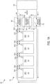
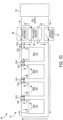
- FIGS. 1A-1F are diagrams of an overview of an example implementation 100 described herein;
- Example implementation 100 may include a bypassable battery module system 1 10, a first bypassable battery module 120-1, a second bypassable battery module 120-2, a third bypassable battery module 120-3, a fourth bypassable battery module 120-4, a set of switches 130-1 through 130-8, a precharge circuit 140, an application bus 150, a positive disconnect 160, and a negative disconnect 170.
- Precharge circuit 140 includes a component capable of limiting an amount of current that passes between bypassable battery module system 110 and application bus 150.
- precharge circuit 140 may include a resistive component configured to limit inrush current that passes between bypassable battery module system 110 and application bus 150.
- bypassable battery module system 110 may activate bypassable battery module 120-2 by closing switch 130-3 and opening switch 130-4, thereby causing the output voltage of bypassable battery module system 110 to increase by an amount equal to the voltage of bypassable battery module 120-2.
- the output voltage of bypassable battery module system 1 10 is 100V
- the voltage of application bus 150 may reach 100Y based on bypassable battery modules 120-1 and 120-2 being activated.
- FIGS. 1A-1F include an example implementation 100, it should be understood that other implementations may be different than what is shown in FIGS. 1A-1F .
- the bypassable battery module system may activate bypassable battery modules in a stepwise manner to permit precharging of the application bus.
- the voltage of the application bus may increase to the output voltage of the bypassable battery module system.
- the voltage difference between the output voltage of the bypassable battery module system and the voltage of the application bus might not exceed an amount equal to the voltage of any particular bypassable battery module of the bypassable battery module system. As such, an amount of inrush current is reduced as compared to situations where a voltage difference between the output voltage of a power source and an application bus is substantially equal to the output voltage of the power source.
- some implementations described herein reduce an amount of power loss due. to ohmic heating, permit a reduction in size of precharge circuitry, reduce a number of situations where damage to the system occurs, reduce a cost of the system, and/or the like.
- Solid state driver 210 is connected to at least the gates of both the first solid state switch 230 and the second solid state switch 240. Solid state driver 210 is therefore able to drive both switches . between their respective on and off positions. Further, the source of first solid state switch 230 is connected to the drain of second solid state switch 240. Additionally, both the source of first solid state switch 230 and the drain of second solid state switch 240 are connected to the positive module terminal 250. The drain of first solid state switch 230 is connected to the positive lead of cell stack array 220, and the source of second solid state switch 240 is connected to the negative lead of cell stack array 220 and negative module terminal 260.
- bypassable battery module 200 may include additional components, fewer components, different components, or differently arranged components than those shown in FIG. 2 . Additionally, or alternatively, a set of components (e.g., one or more components) of bypassable battery module 200 may perform one or more functions described as being performed by another set of components of bypassable, battery module 200.
- FIG. 4 is a flow chart of an example process 400 for precharging an application bus by activing bypassable battery modules, of a bypassable battery module system, in a stepwise manner.
- one or more process blocks of FIG. 4 may be performed by bypassable battery module system 310.
- processor 330 of bypassable battery module system 310 may be configured to perform one or more functions associated with process blocks of FIG. 4 .
- one or more functions of process blocks of FIG. 4 may be performed by another component or a group of components separate from or including bypassable battery module system 310, such, as precharge circuit 340, application bus 350, positive disconnect 360, and/or negative disconnect 370.
- process 400 may include activating a first bypassable battery module, of a bypassable battery module system, to precharge an application bus through a precharge circuit (block 410).
- bypassable battery module system 310 may activate a first bypassable battery module 320, of bypassable battery module system 310, to precharge application bus 350.
- each bypassable battery module 320 of bypassable battery module system 310 may be in the bypassed state.
- an output voltage of bypassable battery module system 3 10 may be 0V.
- a voltage (e.g., an application bus voltage) of application bits 350 may be 0V.
- a voltage difference between an output voltage of bypassable battery module system 310 and a voltage of application bus 350 is 0V.
- bypassable battery module system 310 may activate a second bypassable battery module 320, of bypassable battery module system 310, to permit further precharging of application bus 350 based on activating the first bypassable battery module 320, as described below.
- bypassable battery module system 310 may activate a second bypassable battery module 320 based on activating the first bypassable battery module 320.
- bypassable battery module system 310 may activate single bypassable battery modules 320 in a stepwise manner. That is, bypassable battery module system 310 may activate a first bypassable battery module 320, may activate a second bypassable battery module 320, may activate a third bypassable battery module 320, etc. until each respective bypassable battery module 320 of bypassable battery module system 310 is activated.
- bypassable battery module system 310 may activate multiple bypassable battery modules 320 in a stepwise manner. For example, bypassable battery module system 310 may activate a first subset of bypassable battery modules 320, may activate a second subset of bypassable battery modules 320, etc. until each respective bypassable battery module 320 of bypassable battery module system 310 is activated.
- bypassable battery module system 3 10 may activate the second bypassable battery module 320 based on a condition.
- Bypassable battery module system 310 may obtain information from various sensors (e.g., voltage sensors, current sensors, and/or the like), from a data structure, and/or the like, and determine that a condition is satisfied based on the obtained information.
- bypassable battery module system 310 may activate the second bypassable battery module 320 based on a voltage difference between an output voltage, of bypassable battery module system 3 10 and a voltage of application bus 350 satisfying a threshold.
- bypassable battery module system 310 may determine that the voltage difference is less than a threshold (e.g., 5V, 10V, 12V, etc.), and activate the second bypassable battery module 320 based on the voltage difference being less than the threshold.
- a threshold e.g., 5V, 10V, 12V, etc.
- bypassable battery module system 310 may activate the second bypassable battery module 320 based on a current value satisfying a threshold. For example, bypassable battery module system 310 may determine that an amount of current flowing through precharge circuit 340 is less than a threshold (e.g., 2A, 1.5A, 1A, etc.), and activate the second bypassable battery module 320 based on the amount of current being less than the threshold. Alternatively, bypassable battery module system 310 may use a current, value obtained from another component of environment 300.
- a threshold e.g., 2A, 1.5A, 1A, etc.
- bypassable battery module system 310 may activate the second bypassable battery module 320 based on a voltage of application bus 350 satisfying a threshold. For example, bypassable battery module system 310 may determine that a voltage of application bus 350 is greater than a threshold, and activate the second bypassable battery module 320 based on the voltage being greater than the threshold. In some implementations, bypassable battery module system 3 10 may determine the threshold based on a number of bypassable battery modules 320 that are activated and/or voltages of the activated bypassable battery modules 320.
- bypassable battery module system 310 may iteratively activate bypassable battery modules 320 of bypassable battery module system 310 until each respective bypassable battery module 320 of bypassable battery module system 310 is activated.
- bypassable battery module system 310 reduces an amount of current that passes through precharge circuit 340, reduces power loss due to ohmic heating, permits a reduction in size of components of precharge circuit 340, reduces damage to precharge circuit 340, and/or the like.
- bypassable battery module system 310 may close positive disconnect 360 and negative disconnect 370 based on each bypassable battery module 320 (or a threshold number of bypassable battery modules 320) being activated to permit current to pass between bypassable battery module system 310 and application bus 350 through positive disconnect 360 and negative disconnect 370. Additionally, bypassable battery module system 310 may open precharge circuit 340 based on closing positive disconnect 360 and negative disconnect 370 to prevent current from passing through precharge circuit 340.
- process 400 may include additional blocks, fewer blocks, different blocks, or differently arranged blocks than those depicted in FIG. 4 . Additionally, or alternatively, two or more of the blocks of process 400 may be performed in parallel.
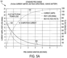
- FIG. 5A is a diagram of an example graph 501 depicting results of a precharge process that is performed by a power source in a non-stepwise manner and that is configured to be completed within a particular amount of time.
- a voltage of application bus 350 increased from an initial value of 0V to substantially 1200V within the time frame of 6 seconds.
- a current value of precharge circuit 340 decreased from a peak current value of 15.18A to substantially 0A within the time frame of 6 seconds.
- a power loss value decreased from a peak power loss value of 18.227 kilowatts (kW) to 0kW within the time frame of 6 seconds.
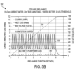
- FIG. 5B is a diagram of an example graph 502 depicting results of a .precharge process that is performed by a bypassable battery module system in a stepwise manner and that is configured to be completed within a particular amount of time.
- FIG. 5B The results shown in FIG. 5B were obtained using a bypassable battery module system 310 including a set of 24 bypassable battery modules 320 including respective voltages of 50V, a precharge circuit 340 including a resistance value of 10 Ohms, and an application bus 350 including a capacitance value of 20 mF.
- a current value of precharge circuit 340 fluctuated between a peak current value of 6.8A and 2A, and reduced to a value of 0A within the time frame of 6 seconds.
- Each fluctuation between 6.SA and 2A corresponds to a respective activation of a particular bypassable battery module 320.
- the peak current value of 6.SA yields a reduction in power loss and a reduction in generated heat.
- a peak power loss value of 426.4W was obtained as compared to the 18kW peak power loss value as shown in FIG. 5A .
- some implementations described herein provided substantially 40 times less power loss than as compared to situations where a power source introduced a total output voltage substantially instantaneously to application bus 350.
- some implementations described herein provided the foregoing benefits using a precharge circuit 340 including a resistance value nearly 8 times less than the resistance value of the precharge circuit 340 of the system of FIG. 5A (e.g., 10 Ohms versus 79 Ohms).
- the results shown in FIG. 6A were obtained using a system including a power source having a voltage of 1200V, a precharge circuit 340 including a resistance value of 5 Ohms, and an application bus 350 including a capacitance value of 20 mF.
- the total voltage (i.e., 1200V) of the power source was introduced substantially instantaneously to application bus 350 through precharge circuit 340.
- bypassable battery module system 310 may initiate a post-discharge process based on an input from another device (e.g., which may have received an input from a user), based on a time frame, based on being connected to application bus 350 for a threshold amount of time, and/or the like.
- another device e.g., which may have received an input from a user
- bypassable battery module system 310 may initiate a post-discharge process based on an input from another device (e.g., which may have received an input from a user), based on a time frame, based on being connected to application bus 350 for a threshold amount of time, and/or the like.
- Bypassable battery module system 3 10 may close precharge circuit 340 to permit current to pass between bypassable battery module system 310 and application bus 350 through precharge circuit 340. Additionally, bypassable battery module system 310 may open positive disconnect 360 and/or negative disconnect 370 to prevent current from passing between bypassable battery module system 310 and application bus 350 through positive disconnect 360 and/or negative disconnect 370.
- Bypassable batter module system 310 may bypass a first bypassable battery module 320, of bypassable battery module system 310, to permit post-discharging of application bus 350 through precharge circuit 340.
- the first bypassable battery module 320 may include a particular bypassable battery module 320 of bypassable battery module system 310.
- bypassable battery module system 310 may bypass a set of bypassable battery modules 320.
- bypassable battery module system 310 may bypass multiple bypassable battery modules 320 where the multiple bypassable battery modules 320 include a subset of bypassable battery modules 320 of bypassable battery module system 310.
- bypassable battery module system 31.0 may initially bypass a single bypassable battery module 320 or bypass a set of bypassable battery modules 320 to permit post-discharging of application bus 350.
- the output voltage of bypassable battery module system 310 may be a total output voltage of bypassable battery module system 310 minus a voltage of the first bypassable battery module 320 based on the first bypassable battery module 320 being bypassed.
- the output voltage of bypassable battery module system 310 may be a sum of the respective voltages of the bypassable battery modules 320 that are in the active state.
- the output voltage of bypassable battery module system 310 may correspond to a total output voltage of bypassable battery module system 310 minus the sum of the voltages of bypassable battery modules 320 that are bypassed.
- a voltage difference between an output voltage of bypassable battery module system 310 and a voltage of application bus 350 may correspond to the voltage of the bypassed battery module(s) 320.
- current may flow from application bus 350 to bypassable battery module system 310 based on the voltage difference.
- the amount of current may depend on the voltage difference and a resistance value of precharge circuit 340.
- a voltage of application bus 350 may decrease based on the current that flows from application bus 350 to bypassable battery module system 310.
- the current may discharge capacitive components of application bus 350, thereby decreasing a voltage of application bus 350.
- a voltage of application bus 350 may be reduced and may be substantially equal to an output voltage of bypassable battery module system 310 based on the first bypassable battery module(s) 320 being bypassed.
- bypassable battery module system 310 may bypass a second bypassable battery module 320, of bypassable battery module system 310, to permit further postdischarging of application bus 350 through precharge circuit 340 based on bypassing the first bypassable battery module 320, as described below.
- process 700 may include bypassing a second bypassable battery module, of the bypassable battery module system, to permit post-discharge of the application bus through the precharge circuit based on bypassing the first bypassable battery module (block 720).
- bypassable battery module system 310 may bypass a second bypassable battery module 320, of bypassable battery module system 310, to permit post-discharge of application bus 350 through precharge circuit 340 based on bypassing the first bypassable battery module 320.
- bypassable battery module system 310 may bypass multiple bypassable battery modules 320 in a stepwise manner. For example, bypassable battery module system 310 may bypass a first subset of bypassable battery modules 320, may bypass a second subset of bypassable battery modules 320, etc. until each respective bypassable battery module 320 of bypassable battery module system 310 is bypassed (or a threshold number of bypassable battery modules 320 are bypassed).
- bypassable battery module system 310 may bypass a second bypassable battery module 320 (or a subset of bypassable battery modules .320) based on one or more conditions as described above in association with block 420 of FIG. 4 .
- bypassable battery module system 310 may bypass a second bypassable battery module 320 based on a voltage difference satisfying a threshold, based on a current value satisfying a threshold, based on a threshold amount of time having elapsed, and/or the like.
- bypassable battery module system 310 may iteratively bypass bypassable battery modules 320 of bypassable battery module system 310 until each respective bypassable battery module 320 of bypassable battery module system is bypassed.
- bypassable battery module system 310 reduces an amount of current that passes through precharge circuit 340, reduces power loss due to ohmic heating, prevents damage to system components, permits a reduction in size of components of precharge circuit 340, and/or the like.
- process 700 may include additional blocks, fewer blocks, different blocks, or differently arranged blocks than those depicted in FIG. 7 . Additionally, or alternatively, two or more of the blocks of process 700 may be performed in parallel.
- FIG. 8 is a diagram of an example graph 800 depicting results of a post-discharge process that is performed by a bypassable battery module system in a stepwise manner.
- bypassable battery module system 310 including 24 bypassable battery modules 320 having respective voltages of 50V, a precharge circuit 340 including a resistance value of 5 Ohms, and an application bus 350 including a capacitance value of 20 mF.
- Bypassable battery module system 310 bypassed respective bypassable battery modules 320 in a stepwise manner.
- a voltage of application bus 350 decreased from an initial value and peak voltage of 1200V to 0V within a time frame of 1.6 seconds.
- a current value of precharge circuit 340 fluctuated between a peak value of 13.6A and 4A within the time frame of 1.6 seconds.
- Each respective peak and trough corresponds to a particular bypassable battery module 320 being bypassed.
- a power loss value fluctuated between a peak power loss value of 0.925 kW and 0kW within the time frame of 1.6 seconds.
- some implementations described herein improve precharge and post-discharge operations of battery systems by permitting stepwise precharge and/or post-discharge. Further, some implementations described herein reduce an amount of current that passes through precharge circuitry during such processes, thereby reducing an amount of power loss due to ohmic heating. Still further, some implementations described herein permit a reduction in size of components and/or permit a reduction in a number of components of precharge circuitry.
- the term component is intended to be broadly construed as hardware, firmware, or a combination of hardware and software.
- satisfying a threshold may refer to a value being greater than the threshold, more than the threshold, higher than the threshold, greater than or equal to the threshold, less than the threshold, fewer than the threshold, lower than the threshold, less than or equal to the threshold, equal to the threshold, etc.
- the articles “a” and “an” are intended to include one or more items, and may be used interchangeably with “one or more.”
- the term “set” is intended to include one or more items (e.g., related items, unrelated items, a combination of related and unrelated items, etc.), and may be used interchangeably with “one or more.” Where only one item is intended, the term “one” or similar language: is used.
- the terms “has,” “have,” “having,” or the like are intended to be open-ended terms. Further, the phrase “based on” is intended to mean “based, at least in part, on” unless explicitly stated otherwise.
Landscapes
- Engineering & Computer Science (AREA)
- Power Engineering (AREA)
- Charge And Discharge Circuits For Batteries Or The Like (AREA)
Description
- Apparatuses and methods consistent with example embodiments relate to a bypassable battery module system and a method for activating and bypassing bypassable battery modules, of the bypassable battery module system, in a stepwise manner to precharge and post-discharge an application bus..
- Precharging refers to a mode of operation in a high voltage direct current (DC) application in which inrush current is limited during an initial power-up procedure of the application. A high voltage system with a large capacitive load can be exposed to a large amount of electric current during the initial power-up of the application. If unlimited, the electric current can cause considerable stress ' and damage to system components. Precharging attempts to mitigate deleterious effects by limiting the magnitude of the inrush current. Further, post-discharging refers to a mode of operation in which application bus voltage is discharged back into a power source during shutdown of an application. Post-discharging can further reduce deleterious effects associated with high capacitance applications.
- According to the invention there is proposed a method for charging an application bus through a battery module system according to
claim 1 and a system for precharging an application bus according toclaim 4. Embodiments of the invention are defined in the dependent claims. -
-
FIGS, 1A-1F are diagrams of an overview of an example implementation described herein; -
FIG. 2 is a diagram of an example bypassable battery module described herein; -
FIG. 3 is a diagram _of an example environment in which systems and/or methods, described herein, may be implemented: -
FIG. 4 is a flow chart of an example process for precharging an application bus by activing bypassable battery modules, of a bypassable battery module system, in a stepwise manner; -
FIG. 5A is a diagram of an example graph depicting results of a precharge process that is performed by a power source in a non-stepwise manner and that is configured to be completed within a particular amount of time; -
FIG. 5B is a diagram of an example graph depicting results of a precharge process that is performed by a bypassable battery module system in a stepwise manner and that is configured to be completed within a particular amount of time; -
FIG. 6A is a diagram of an example graph depicting results of a precharge process that is performed by a power source in a non-stepwise manner and that is performed using a precharge circuit having a particular resistance value; -
FIG. 6B is a _diagram of an example graph depicting results of a precharge process that is performed by a bypassable battery module system in a stepwise manner and that is performed using a precharge circuit having a particular resistance value; -
FIG. 7 is a flow chart of an example process for post-discharging an application bus by bypassing bypassable battery modules, of a bypassable battery module system, in a stepwise manner; and -
FIG. 5 is a diagram of an example graph depicting results of a post-discharge process that is performed by a bypassable battery module system in a stepwise manner. - The following detailed description of example implementations refers to the accompanying drawings. The same reference numbers in different drawings may identify the same or similar elements.
- A high voltage (e.g., 1000 volts tVi, 1200V. 1600V, etc.) power source and precharge circuitry can be used to precharge an application bus having a high capacitance (e.g., 10 millifarads (mF), 20 mF, 35 mF, etc.). In a situation where the high voltage power source is connected to the application bus through the precharge circuitry, a voltage difference, between an output voltage of the high voltage power source and a voltage of the application bus may cause deleterious effects. For example a large voltage difference (e.g., 1000V, 1200V, 1600V, etc.) may cause extensive ohmic heating as inrush current passes through the precharge circuitry based on the voltage difference. As a result, physically large precharge circuitry components and/or cooling components may be required to be implemented to dissipate heat generated during the precharge process. Similarly, the cost of the precharge circuitry is commensurately increased.
- Some implementations described herein provide a bypassable battery module system that may activate bypassable battery modules, of the bypassable battery module system, in a stepwise manner to precharge an application bus. In this way, a voltage difference between the bypassable battery module system and the application bus is reduced as compared to situations where the entire voltage, of a power source, is introduced to the application bus substantially instantaneously. Thereby, some implementations described herein reduce an amount of current that passes through the precharge circuitry, reduce an amount of ohmic heating, reduce power loss, and/or the like, during the precharge process. In this way, some implementations described herein permit physically smaller precharge circuitry components to be used during the precharge process, reduce cost associated with such components, reduce a number of situations where components - associated with the power source, precharge circuitry, and/or application bus are damaged or destroyed, and/or the like.
-
FIGS. 1A-1F are diagrams of an overview of anexample implementation 100 described herein;Example implementation 100 may include a bypassablebattery module system 1 10, a first bypassable battery module 120-1, a second bypassable battery module 120-2, a third bypassable battery module 120-3, a fourth bypassable battery module 120-4, a set of switches 130-1 through 130-8, aprecharge circuit 140, anapplication bus 150, apositive disconnect 160, and anegative disconnect 170. - Bypassable battery module system _ 1 10 includes a component capable of selectively activating and/or bypassing bypassable battery modules 120-1 through 120-4 to permit stepwise precharge and/or post-discharge of
application bus 150. Bypassablebattery module system 1 10 includes a set of bypassable battery modules 120-1 through 120-4 connected in series that are each capable of being in an active state or a bypassed state. - In the active state, a voltage of
bypassable battery module 120 may contribute to an output voltage of bypassablebattery module system 110, In the bypassed state, a voltage ofbypassable battery module 120 may not contribute to an output voltage of bypassable -battery module system 110. In this way, bypassablebattery module system 110 may adjust an output voltage of bypassablebattery module system 1 10 based on the number ofbypassable battery modules 120 that are in the active state. - Bypassable battery modules 120-1 through 120-4 include components capable -of being selectively activated and/or bypassed to permit stepwise precharge and/or post-discharge of
application bus 150. For example, each bypassable battery module 120-1 through 120-4 includes a 50V power source that may be selectively connected toapplication bus 150 by switches 130-1 through 130-8. - Switches 130-1 through 130-8 include components capable of selectively connecting battery modules 120-1 through 120-4 to
application bus 150. For example, bypassablebattery module system 110 may selectively control switches 130-1 through 130-8 to connect or disconnectbypassable battery modules 120, thereby adjusting an output voltage of bypassablebattery module system 110. -
Precharge circuit 140 includes a component capable of limiting an amount of current that passes between bypassablebattery module system 110 andapplication bus 150. For example,precharge circuit 140 may include a resistive component configured to limit inrush current that passes between bypassablebattery module system 110 andapplication bus 150. -
Positive disconnect 160 andnegative disconnect 170 include components capable of permitting or preventing current to pass between bypassablebattery module system 1 10 andapplication bus 150. For examplepositive disconnect 160 and/ornegative disconnect 170 may include a switching component capable of being selectively switched to permit or prevent current from passing between bypassablebattery module system 1 10 andapplication bus 150. - As shown in
FIG. 1A , bypassablebattery module system 1 10 may closeprecharge circuit 140 to permit current to pass from bypassablebattery module system 110 toapplication bus 150 throughprecharge circuit 140. As further shown in .FIG. 1 A , eachbypassable battery module 120 is in the bypassed state. For example as shown inFIG. 1A , each respective switch 130 may be open, thereby preventing respective voltages ofbypassable battery modules 120 from being connected toapplication bus 150. As such, an output voltage of bypassable battery module,system 110 is 0V because each respectivebypassable battery module 120 is being bypassed. - As shown in
FIG. 1B , bypassablebattery module system 110 may activate bypassable battery module 120-1 by closing -switch 130-1 and opening switch 130-2, thereby causing the output voltage of bypassablebattery module system 110 to increase by an amount equal to the voltage of bypassable battery module 120-1. In this case, the output voltage of bypassablebattery module system 110 is 50V, and a . voltage difference between the output voltage of bypassablebattery module system 110 and a voltage ofapplication bus 150 is 50V (e.g., 50V - 0V = 50V). The voltage difference may cause inrush current to pass throughprecharge circuit 140 intoapplication bus 150, thereby permitting capacitive components ofapplication bus 150 to be charged. As such, the voltage ofapplication 150 bus may reach 50V based on bypassable battery module 120-1 being activated. - As shown in
FIG. 1C , bypassablebattery module system 110 may activate bypassable battery module 120-2 by closing switch 130-3 and opening switch 130-4, thereby causing the output voltage of bypassablebattery module system 110 to increase by an amount equal to the voltage of bypassable battery module 120-2. In this case, the output voltage of bypassablebattery module system 1 10 is 100V, and the voltage difference between the output voltage of bypassablebattery module system 110 and the voltage ofapplication bus 150 is 50V (e.g., 100V - 50V = 50V). As such, the voltage ofapplication bus 150 may reach 100Y based on bypassable battery modules 120-1 and 120-2 being activated. - As shown in
FIG. 1D , bypassablebattery module system 110 may activate bypassable battery module 120-3 by closing switch 130-5 and opening switch 130-6, thereby causing the output voltage of bypass ablebattery module system 110 to increase by an amount equal to the voltage of bypassable battery module 120-3. in this case, the output voltage of bypassablebattery module system 110 is 150V, and the voltage difference between the output voltage of bypassablebattery module system 110 and the voltage ofapplication bus 150 is 50V (e.g., 150V - 100V = 50V). As such, the voltage of application bus 1.50 may reach 150V based on bypassable battery modules 120-1 through 120-3 being activated. - As shown in
FIG. 1E . bypassablebattery module system 110 may activate bypassable battery module 120-4 by closing switch 130-7 and opening switch 130-8, thereby causing an output voltage of bypassablebattery module system 110 to increase by an amount equal to the voltage of bypassable battery module 120-4, In this case, the output voltage of bypassablebattery module system 110 is 200V, and the voltage difference between the output voltage of bypassablebattery module system 110 and the voltage ofapplication bus 150 is 50V (e.g., 200V - 150V = 50V). As such, the voltage ofapplication bus 150 may reach 200V based on bypassable battery modules 120-1 through 120-4 being activated. - As shown in
FIG. 1F , bypassablebattery module system 110 may closepositive disconnect 160 andnegative disconnect 170 to permit current to pass between bypassablebattery module system 110 andapplication bus 150 throughpositive disconnect 160 andnegative disconnect 170. - While
FIGS. 1A-1F include anexample implementation 100, it should be understood that other implementations may be different than what is shown inFIGS. 1A-1F . - In this way, the bypassable battery module system may activate bypassable battery modules in a stepwise manner to permit precharging of the application bus. Additionally, the voltage of the application bus may increase to the output voltage of the bypassable battery module system. Still further, the voltage difference between the output voltage of the bypassable battery module system and the voltage of the application bus might not exceed an amount equal to the voltage of any particular bypassable battery module of the bypassable battery module system. As such, an amount of inrush current is reduced as compared to situations where a voltage difference between the output voltage of a power source and an application bus is substantially equal to the output voltage of the power source.
- As such, some implementations described herein reduce an amount of power loss due. to ohmic heating, permit a reduction in size of precharge circuitry, reduce a number of situations where damage to the system occurs, reduce a cost of the system, and/or the like.
-
FIG. 2 is a diagram of an examplebypassable battery module 200 described herein; As shown inFIG. 2 ,bypassable battery module 200 may include asolid state driver 210, acell stack array 220, a firstsolid state switch 230, a secondsolid state switch 240, apositive module terminal 250, and anegative module terminal 260. -
Solid state driver 210 is connected to at least the gates of both the firstsolid state switch 230 and the secondsolid state switch 240.Solid state driver 210 is therefore able to drive both switches . between their respective on and off positions. Further, the source of firstsolid state switch 230 is connected to the drain of secondsolid state switch 240. Additionally, both the source of firstsolid state switch 230 and the drain of secondsolid state switch 240 are connected to thepositive module terminal 250. The drain of firstsolid state switch 230 is connected to the positive lead ofcell stack array 220, and the source of secondsolid state switch 240 is connected to the negative lead ofcell stack array 220 andnegative module terminal 260. - Accordingly, when first
solid state switch 230 is in an on-state and secondsolid state switch 240 is in an off-state, as controlled bysolid state driver 210,cell stack array 220 ofbypassable battery module 200 is engaged and connected through positiveterminal module 250 andnegative module terminal 260. In this case,bypassable battery module 200 is in the activated state. - Alternatively, when first
solid state switch 230 is in an off-state and secondsolid state switch 240 is in an on-state, as controlled bysolid state driver 210,cell stack array 220 ofbypassable battery module 200 is effectively disengaged and bypassed by allowing positiveterminal module 250 andnegative module terminal 260 to be connected through secondsolid state switch 240 which is in an on-state. In this case,bypassable battery module 200 is in the bypassed state. -
Bypassable battery module 200 is described in more detail inU.S. Patent No. 9.525.290 - The number and arrangement of components shown in
FIG. 2 are provided as an example. In practice,bypassable battery module 200 may include additional components, fewer components, different components, or differently arranged components than those shown inFIG. 2 . Additionally, or alternatively, a set of components (e.g., one or more components) ofbypassable battery module 200 may perform one or more functions described as being performed by another set of components of bypassable,battery module 200. -
FIG. 3 is a diagram of anexample environment 300 in which systems and/or methods, described herein, may be implemented. As shown inFIG. 3 ,environment 300 may include a bypassablebattery module system 310, a set of bypassable battery modules 320-1 through 320-N (N ≥ 2), aprocessor 330, aprecharge circuit 340, anapplication bus 350, apositive disconnect 360, and anegative disconnect 370. - Bypassable
battery module system 310 includes a component that may selectively activate or bypass bypassable battery module 320-1 through bypassable battery module 320-N. Bypassablebattery module system 310 andbypassable battery module 320 are described in more detail in association withU.S. Patent No. 9,525,290 U.S. Patent No. 9,525,290 -
Processor 330 is implemented in hardware, firmware, or a combination of hardware and software.Processor 330 may include a processor (e.g., a central processing unit (CPU), an accelerated processing unit (APU), etc.), a microprocessor, a controller, a microcontroller, and/or any other type of processing component (e.g., a field-programmable gate array (FPGA), an application-specific integrated circuit (ASIC), etc.) that interprets and/or executes instructions. - In some implementations,
processor 330 may include one or more processors capable of being programmed to perform a function. A memory, such as a random access memory (RAM), a read only memory (ROM), a flash memory, an optical memory, etc., may store: information and/or instructions for use byprocessor 330. In some implementations,processor 330 may obtain information from one or more sensors (e.g., voltage sensors, current sensors, , heat sensors, and/or the like), from a data structure, and/or the like, and perform one or more actions based on the obtained information. The one or more sensors may be associated with any of the components described in connection withFIG. 3 . -
Precharge circuit 340 includes a component capable of permitting current to pass between bypassablebattery module system 310 andapplication bus 350. In some implementations,precharge circuit 340 includes a current-limiting component including a particular resistance value. For example, precharge circuit includes one or more components, such as a resistor, a connector, a transistor, a capacitor, a switch, and/or the like. -
Application bus 350 includes a component capable of connecting a load to bypassablebattery module system 310. In some implementations,application bus 350 includes a capacitive component. For example,application bus 350 includes one or more components, such as a capacitor, a transistor, a switch, a resistor, and/or the like.Positive disconnect 360 includes a component capable of permitting current to pass between bypassablebattery module system 3 10 andapplication bus 350.Negative disconnect 370 includes a component capable of permitting current to pass between bypassablebattery module system 310 andapplication bus 350. - The number and arrangement of components shown in
FIG. 3 are provided as an example. In practice,environment 300 may include additional components, fewer components, different components, or differently arranged components than those shown inFIG. 3 . Additionally, or alternatively, a set of components (e.g., one or more components) ofenvironment 300 may perform one or more functions described as being performed by another set of components ofenvironment 300. -
FIG. 4 is a flow chart of anexample process 400 for precharging an application bus by activing bypassable battery modules, of a bypassable battery module system, in a stepwise manner. In some implementations, one or more process blocks ofFIG. 4 may be performed by bypassablebattery module system 310. For example,processor 330 of bypassablebattery module system 310 may be configured to perform one or more functions associated with process blocks ofFIG. 4 . Alternatively, one or more functions of process blocks ofFIG. 4 may be performed by another component or a group of components separate from or including bypassablebattery module system 310, such, asprecharge circuit 340,application bus 350,positive disconnect 360, and/ornegative disconnect 370. - As shown in
FIG. 4 ,process 400 may include activating a first bypassable battery module, of a bypassable battery module system, to precharge an application bus through a precharge circuit (block 410). For example, bypassablebattery module system 310 may activate a firstbypassable battery module 320, of bypassablebattery module system 310, toprecharge application bus 350. - In some implementations, bypassable
battery module system 3 10 may initiate a precharge process based on an input from another device (e.g., which may have received an input from a user), based on a time frame, based on being connected toapplication bus 350, and/or the like. - Bypassable
battery module system 310 may openpositive disconnect 360 and/ornegative disconnect 370 to prevent current from passing between bypassablebattery module system 310 andapplication bus 350 throughpositive disconnect 360 and/ornegative disconnect 370. Additionally, bypassablebattery module system 310 may closeprecharge circuit 340 to permit current to pass between bypassablebattery module system 310 andapplication bus 350 throughprecharge circuit 340. - Initially, each
bypassable battery module 320 of bypassablebattery module system 310 may be in the bypassed state. As such, an output voltage of bypassablebattery module system 3 10 may be 0V. Additionally, a voltage (e.g., an application bus voltage) ofapplication bits 350 may be 0V. In this case, a voltage difference between an output voltage of bypassablebattery module system 310 and a voltage ofapplication bus 350 is 0V. - Bypassable
battery module system 310 may activate a firstbypassable battery module 320, of bypassablebattery module system 310, to permit precharging ofapplication bus 350 throughprecharge circuit 340. For example, the firstbypassable battery module 320 may include a particularbypassable battery module 320 of bypassablebattery module system 310. Additionally, or alternatively, bypassablebattery module system 310 may activate a set ofbypassable battery modules 320. For example, bypassablebattery module system 310 may activate multiplebypassable battery modules 320 where the multiplebypassable battery modules 320 include a subset ofbypassable battery modules 320 of bypassablebattery module system 310. In other words, bypassablebattery module system 310 may initially activate a singlebypassable battery module 320 or a set ofbypassable battery modules 320 to permit precharging ofapplication bus 350. - The output voltage of bypassable
battery module system 310 may be a voltage of the firstbypassable battery module 320 based on the firstbypassable battery module 320 being activated. For example, in the situation where -a singlebypassable battery module 320 is activated, the output voltage of bypassablebattery module system 310 may correspond to a voltage of .the singlebypassable battery module 320 that is activated. Alternatively, in the situation where multiplebypassable battery modules 320 are activated, the output voltage of bypassablebattery module system 310 may correspond to a sum of the voltages of thebypassable battery modules 320 that are activated. - A voltage difference between an output voltage of bypassable
battery module system 310 and a voltage ofapplication bus 350 may correspond to the voltage of the activated bypassable battery module(s) 320. In this case, current may flow from bypassable :battery module system 310 toapplication bus 350 based on the voltage difference. The amount of current may depend on the voltage difference and a resistance value ofprecharge circuit 340. - A voltage of
application bus 350 may increase based on the current that flows from bypassablebattery module system 310 toapplication bus 350. For example, the current may charge capacitive components ofapplication bus 350, thereby increasing a voltage ofapplication bus 350. In this way, a voltage ofapplication bus 350 may be substantially equal to an output voltage of bypassablebattery module system 310 based on bypassable battery module(s) 320 being activated. - In this way, bypassable
battery module system 310 may activate a secondbypassable battery module 320, of bypassablebattery module system 310, to permit further precharging ofapplication bus 350 based on activating the firstbypassable battery module 320, as described below. - As further shown in
FIG. 4 ,process 400 may include activating a second bypassable battery module, of the bypassable battery module system, to precharge the application bus through the precharge circuit based on activating the first bypassable battery module (block 420). For example, bypassablebattery module system 310 may activate a secondbypassable battery module 320, of bypassablebattery module system 310, toprecharge application bus 350 based on activating the firstbypassable battery module 320, - In some implementations, bypassable
battery module system 310 may activate a secondbypassable battery module 320 based on activating the firstbypassable battery module 320. For example, bypassablebattery module system 310 may activate singlebypassable battery modules 320 in a stepwise manner. That is, bypassablebattery module system 310 may activate a firstbypassable battery module 320, may activate a secondbypassable battery module 320, may activate a thirdbypassable battery module 320, etc. until each respectivebypassable battery module 320 of bypassablebattery module system 310 is activated. - Alternatively, bypassable
battery module system 310 may activate multiplebypassable battery modules 320 in a stepwise manner. For example, bypassablebattery module system 310 may activate a first subset ofbypassable battery modules 320, may activate a second subset ofbypassable battery modules 320, etc. until each respectivebypassable battery module 320 of bypassablebattery module system 310 is activated. - In some implementations, bypassable
battery module system 3 10 may activate the secondbypassable battery module 320 based on a condition. Bypassablebattery module system 310 may obtain information from various sensors (e.g., voltage sensors, current sensors, and/or the like), from a data structure, and/or the like, and determine that a condition is satisfied based on the obtained information. - For example, bypassable
battery module system 310 may activate the secondbypassable battery module 320 based on a voltage difference between an output voltage, of bypassablebattery module system 3 10 and a voltage ofapplication bus 350 satisfying a threshold. According to the invention, bypassablebattery module system 310 may determine that the voltage difference is less than a threshold (e.g., 5V, 10V, 12V, etc.), and activate the secondbypassable battery module 320 based on the voltage difference being less than the threshold. - Alternatively but not within the scope of the invention, Alternatively, bypassable
battery module system 310 may activate the secondbypassable battery module 320 based on a threshold amount of time having elapsed since the firstbypassable battery module 320 was activated. For example, bypassablebattery module system 310 may determine that a threshold amount of time (e.g., 5 milliseconds (ms), 10 ms, 2.5 ms, etc.) has elapsed since the firstbypassable battery module 320 was activated, and activate, the secondbypassable battery module 320 based on the threshold amount of time having elapsed. - Alternatively but not within the scope of the invention, bypassable
battery module system 310 may activate the secondbypassable battery module 320 based on a current value satisfying a threshold. For example, bypassablebattery module system 310 may determine that an amount of current flowing throughprecharge circuit 340 is less than a threshold (e.g., 2A, 1.5A, 1A, etc.), and activate the secondbypassable battery module 320 based on the amount of current being less than the threshold. Alternatively, bypassablebattery module system 310 may use a current, value obtained from another component ofenvironment 300. - Alternatively but not within the scope of the invention, bypassable
battery module system 310 may activate the secondbypassable battery module 320 based on a voltage ofapplication bus 350 satisfying a threshold. For example, bypassablebattery module system 310 may determine that a voltage ofapplication bus 350 is greater than a threshold, and activate the secondbypassable battery module 320 based on the voltage being greater than the threshold. In some implementations, bypassablebattery module system 3 10 may determine the threshold based on a number ofbypassable battery modules 320 that are activated and/or voltages of the activatedbypassable battery modules 320. - Alternatively but not within the scope of the invention, bypassable
battery module system 310 may activate the secondbypassable battery module 320 based on a power value satisfying a .threshold. For example, bypassablebattery module system 310 may determine a power value based on a current value and a resistance value ofprecharge circuit 340, and activate the secondbypassable battery module 320 based on the power value being less than a threshold. - In some implementations, bypassable
battery module system 310 may iteratively activatebypassable battery modules 320 of bypassablebattery module system 310 until each respectivebypassable battery module 320 of bypassablebattery module system 310 is activated. By activatingbypassable battery modules 320 in a stepwise manner, bypassablebattery module system 310 reduces an amount of current that passes throughprecharge circuit 340, reduces power loss due to ohmic heating, permits a reduction in size of components ofprecharge circuit 340, reduces damage toprecharge circuit 340, and/or the like. - Additionally, bypassable
battery module system 310 may closepositive disconnect 360 andnegative disconnect 370 based on each bypassable battery module 320 (or a threshold number of bypassable battery modules 320) being activated to permit current to pass between bypassablebattery module system 310 andapplication bus 350 throughpositive disconnect 360 andnegative disconnect 370. Additionally, bypassablebattery module system 310 may openprecharge circuit 340 based on closingpositive disconnect 360 andnegative disconnect 370 to prevent current from passing throughprecharge circuit 340. - Although
FIG. 4 shows example blocks ofprocess 400, in some implementations,process 400 may include additional blocks, fewer blocks, different blocks, or differently arranged blocks than those depicted inFIG. 4 . Additionally, or alternatively, two or more of the blocks ofprocess 400 may be performed in parallel. -
FIG. 5A . is a diagram of anexample graph 501 depicting results of a precharge process that is performed by a power source in a non-stepwise manner and that is configured to be completed within a particular amount of time. - The results shown in
FIG. 5A were obtained using a system including a power source including a voltage of 1200V, aprecharge circuit 340 including a resistance value of 79 Ohms, and anapplication bus 350 including a capacitance value of 20 mF. The system was configured to substantially complete the precharge process in a time frame of 6 seconds. Further, the entire voltage (i.e., 1200V) of the power source was introduced substantially instantaneously toapplication bus 350 throughprecharge circuit 340. - As shown in
FIG. 5A , and byreference number 510, a voltage ofapplication bus 350 increased from an initial value of 0V to substantially 1200V within the time frame of 6 seconds. - As further shown in
FIG. 5A , and byreference number 520, a current value ofprecharge circuit 340 decreased from a peak current value of 15.18A to substantially 0A within the time frame of 6 seconds. - As further shown in
FIG. 5A . and byreference number 530, a power loss value decreased from a peak power loss value of 18.227 kilowatts (kW) to 0kW within the time frame of 6 seconds. -
FIG. 5B is a diagram of anexample graph 502 depicting results of a .precharge process that is performed by a bypassable battery module system in a stepwise manner and that is configured to be completed within a particular amount of time. - The results shown in
FIG. 5B were obtained using a bypassablebattery module system 310 including a set of 24bypassable battery modules 320 including respective voltages of 50V, aprecharge circuit 340 including a resistance value of 10 Ohms, and anapplication bus 350 including a capacitance value of 20 mF. The bypassablebattery module system 310 was configured to substantially complete the precharge process in a time frame of 6 seconds. Further, the total output voltage (i.e., 50V × 24 = 1200V) of bypassablebattery module system 310 was introduced in a stepwise -manner toapplication bus 350. - As shown in
FIG. 5B , and byreference number 540, a voltage ofapplication bus 350 increased from an initial value of 0V to substantially 1200V within the time frame of 6 seconds. - As further shown in
FIG. 5B , and byreference number 550, a current value ofprecharge circuit 340 fluctuated between a peak current value of 6.8A and 2A, and reduced to a value of 0A within the time frame of 6 seconds. Each fluctuation between 6.SA and 2A corresponds to a respective activation of a particularbypassable battery module 320. As compared with the results ofFIG. 5A , namely the peak current value of 15.18A, the peak current value of 6.SA yields a reduction in power loss and a reduction in generated heat. - As further shown in
FIG. 5B , and byreference number 560, a peak power loss value of 426.4W was obtained as compared to the 18kW peak power loss value as shown inFIG. 5A . As such, some implementations described herein provided substantially 40 times less power loss than as compared to situations where a power source introduced a total output voltage substantially instantaneously toapplication bus 350. Additionally, some implementations described herein provided the foregoing benefits using aprecharge circuit 340 including a resistance value nearly 8 times less than the resistance value of theprecharge circuit 340 of the system ofFIG. 5A (e.g., 10 Ohms versus 79 Ohms). -
FIG. 6A is a diagram of anexample graph 601 depicting results of a precharge process that is performed by a power source in a non-stepwise manner and that is performed using a precharge circuit having a particular resistance value. - The results shown in
FIG. 6A were obtained using a system including a power source having a voltage of 1200V, aprecharge circuit 340 including a resistance value of 5 Ohms, and anapplication bus 350 including a capacitance value of 20 mF. The total voltage (i.e., 1200V) of the power source was introduced substantially instantaneously toapplication bus 350 throughprecharge circuit 340. - As shown in
FIG. 6A , and byreference number 610, a voltage ofapplication bus 350 increased from an initial value of 0V to substantially 1200V in a time frame of 0.45 seconds. - As further shown in
FIG. 6A , and byreference number 620, a current value ofprecharge circuit 340 decreased from a peak current value of substantially 240A to 0A within the time frame of 0.45 seconds. - As further shown in
FIG. 6A , and byreference number 630, a power loss value decreased from a peak power loss value of 288k W to 0kW within the time frame of 0.45 seconds. -
FIG. 6B is a diagram of an example graph depicting results of a precharge process that is performed by a bypassable battery module system in a stepwise manner and that is performed using a precharge circuit having the particular resistance value. - The results shown in
FIG. 6B were obtained using bypassablebattery module system 310 including a set of 24bypassable battery modules 320 including respective voltages of 50V, aprecharge circuit 340 including a resistance value of 5 Ohms, and anapplication bus 350 including a capacitance value of 20 mF. The total voltage (i.e., 50V × 24 = 1200V) of bypassablebattery module system 310 was introduced in a stepwise manner toapplication bus 350. - As shown in
FIG. 6B , and byreference number 640, a voltage ofapplication bus 350 increased from an initial value of 0V to substantially 1200V within a time frame of 1 .f_, seconds. - As further shown in
FIG. 6B , and byreference number 650, a current value ofprecharge circuit 340 fluctuated between a peak value of 13.6A and 4A, and reduced to 0A within the time frame of 1.6 seconds. As compared toFIG. 6A , the peak current value of 13.6A was nearly 1.8 times lower than the peak current value of 240A as shown inFIG. 6A . - As further shown in
FIG. 6B , and byreference number 660, a power loss value fluctuated between a peak power loss value of 0.924kW and 0kW within the time frame of 1.6 seconds. As compared toFIG. 6A , the peak power loss value of 0.924kW is over 300 times less than the peak power loss value of 288kW shown inFIG. 6A . -
FIG. 7 is a flow chart of anexample process 700 for post-discharging an application bus by bypassing bypassable battery modules, of a bypassable battery module system, in a stepwise manner. In some implementations, one or more process blocks ofFIG. 7 may be performed by bypassablebattery module system 310. For example,processor 330 of bypassablebattery module system 310 may be configured to perform one or more functions of process blocks ofFIG. 7 . Alternatively, one or more functions of process blocks ofFIG. 7 may be performed by another component or a group of components separate from or including bypassablebattery module system 310, such asprecharge circuit 340,application bus 350,positive disconnect 360, and/ornegative disconnect 370. - As shown in
FIG. 7 ,process 700 may include bypassing a first bypassable battery module, of a bypassable battery module system, to post-discharge an application bus through a precharge circuit (block 710). For example, bypassablebattery module system 310 may bypass a firstbypassable battery module 320, of bypassablebattery module system 310, topost-discharge application bus 350 throughprecharge circuit 340. - In some implementations, bypassable
battery module system 310 may initiate a post-discharge process based on an input from another device (e.g., which may have received an input from a user), based on a time frame, based on being connected toapplication bus 350 for a threshold amount of time, and/or the like. - Bypassable
battery module system 3 10 may closeprecharge circuit 340 to permit current to pass between bypassablebattery module system 310 andapplication bus 350 throughprecharge circuit 340. Additionally, bypassablebattery module system 310 may openpositive disconnect 360 and/ornegative disconnect 370 to prevent current from passing between bypassablebattery module system 310 andapplication bus 350 throughpositive disconnect 360 and/ornegative disconnect 370. - Initially, each
bypassable battery module 320 of bypassablebattery module system 310 may be in the activated state. As such, an output voltage of bypassablebattery module system 310 may be equal to the sum of the respective voltages of eachbypassable battery module 320 that is in the activated state (e.g., a total voltage). Additionally, , a voltage ofapplication bus 350 may be equal to the output voltage of bypassablebattery module system 310. In this case, a voltage difference between an output voltage of bypassablebattery module system 310 and a voltage ofapplication bus 350 is 0V. - Bypassable
batter module system 310 may bypass a firstbypassable battery module 320, of bypassablebattery module system 310, to permit post-discharging ofapplication bus 350 throughprecharge circuit 340. For example, the firstbypassable battery module 320 may include a particularbypassable battery module 320 of bypassablebattery module system 310. Additionally, or alternatively, bypassablebattery module system 310 may bypass a set ofbypassable battery modules 320. For example, bypassablebattery module system 310 may bypass multiplebypassable battery modules 320 where the multiplebypassable battery modules 320 include a subset ofbypassable battery modules 320 of bypassablebattery module system 310. In other words, bypassable battery module system 31.0 may initially bypass a singlebypassable battery module 320 or bypass a set ofbypassable battery modules 320 to permit post-discharging ofapplication bus 350. - The output voltage of bypassable
battery module system 310 may be a total output voltage of bypassablebattery module system 310 minus a voltage of the firstbypassable battery module 320 based on the firstbypassable battery module 320 being bypassed. In other words, the output voltage of bypassablebattery module system 310 may be a sum of the respective voltages of thebypassable battery modules 320 that are in the active state. Alternatively, in the situation where multiplebypassable battery modules 320 are bypassed, then the output voltage of bypassablebattery module system 310 may correspond to a total output voltage of bypassablebattery module system 310 minus the sum of the voltages ofbypassable battery modules 320 that are bypassed. - A voltage difference between an output voltage of bypassable
battery module system 310 and a voltage of application bus 350may correspond to the voltage of the bypassed battery module(s) 320. In this case, current may flow fromapplication bus 350 to bypassablebattery module system 310 based on the voltage difference. The amount of current may depend on the voltage difference and a resistance value ofprecharge circuit 340. - A voltage of
application bus 350 may decrease based on the current that flows fromapplication bus 350 to bypassablebattery module system 310. For example, the current may discharge capacitive components ofapplication bus 350, thereby decreasing a voltage ofapplication bus 350. In this way, a voltage ofapplication bus 350 may be reduced and may be substantially equal to an output voltage of bypassablebattery module system 310 based on the first bypassable battery module(s) 320 being bypassed. - In this way, bypassable
battery module system 310 may bypass a secondbypassable battery module 320, of bypassablebattery module system 310, to permit further postdischarging ofapplication bus 350 throughprecharge circuit 340 based on bypassing the firstbypassable battery module 320, as described below. - As further shown in
FIG. 7 ,process 700 may include bypassing a second bypassable battery module, of the bypassable battery module system, to permit post-discharge of the application bus through the precharge circuit based on bypassing the first bypassable battery module (block 720). For example, bypassablebattery module system 310 may bypass a secondbypassable battery module 320, of bypassablebattery module system 310, to permit post-discharge ofapplication bus 350 throughprecharge circuit 340 based on bypassing the firstbypassable battery module 320. - In some implementations, bypassable
battery module system 310 may bypass a secondbypassable battery module 320 based on bypassing the firstbypassable battery module 320. For example, bypassablebattery module system 310 may bypass singlebypassable battery modules 320 in a stepwise manner. That is, bypassablebattery module system 310 may bypass a firstbypassable battery module 320, may bypass a secondbypassable battery module 320, may bypass a thirdbypassable battery module 320, etc. until each respectivebypassable battery module 320 of bypassablebattery module system 310 is bypassed. - Alternatively, bypassable
battery module system 310 may bypass multiplebypassable battery modules 320 in a stepwise manner. For example, bypassablebattery module system 310 may bypass a first subset ofbypassable battery modules 320, may bypass a second subset ofbypassable battery modules 320, etc. until each respectivebypassable battery module 320 of bypassablebattery module system 310 is bypassed (or a threshold number ofbypassable battery modules 320 are bypassed). - In some implementations, bypassable
battery module system 310 may bypass a second bypassable battery module 320 (or a subset of bypassable battery modules .320) based on one or more conditions as described above in association withblock 420 ofFIG. 4 . For example, bypassablebattery module system 310 may bypass a secondbypassable battery module 320 based on a voltage difference satisfying a threshold, based on a current value satisfying a threshold, based on a threshold amount of time having elapsed, and/or the like. - In some implementations, bypassable
battery module system 310 may iteratively bypassbypassable battery modules 320 of bypassablebattery module system 310 until each respectivebypassable battery module 320 of bypassable battery module system is bypassed. By bypassingbypassable battery modules 320 in a stepwise manner, bypassablebattery module system 310 reduces an amount of current that passes throughprecharge circuit 340, reduces power loss due to ohmic heating, prevents damage to system components, permits a reduction in size of components ofprecharge circuit 340, and/or the like. - Bypassable
battery module system 310 may openprecharge circuit 340 based bypassing eachbypassable battery module 320 to prevent current from passing throughprecharge circuit 340. - Although
FIG. 7 shows example blocks ofprocess 700, in some implementations,process 700 may include additional blocks, fewer blocks, different blocks, or differently arranged blocks than those depicted inFIG. 7 . Additionally, or alternatively, two or more of the blocks ofprocess 700 may be performed in parallel. -
FIG. 8 is a diagram of anexample graph 800 depicting results of a post-discharge process that is performed by a bypassable battery module system in a stepwise manner. - The results shown in
FIG. 8 were obtained using bypassablebattery module system 310 including 24bypassable battery modules 320 having respective voltages of 50V, aprecharge circuit 340 including a resistance value of 5 Ohms, and anapplication bus 350 including a capacitance value of 20 mF. Bypassablebattery module system 310 bypassed respectivebypassable battery modules 320 in a stepwise manner. - As shown in
FIG. 8 , and byreference number 810, a voltage ofapplication bus 350 decreased from an initial value and peak voltage of 1200V to 0V within a time frame of 1.6 seconds. - As further shown in
FIG. 8 , and byreference number 820, a current value ofprecharge circuit 340 fluctuated between a peak value of 13.6A and 4A within the time frame of 1.6 seconds. Each respective peak and trough corresponds to a particularbypassable battery module 320 being bypassed. - As further shown in
FIG. 8 , and byreference number 830, a power loss value fluctuated between a peak power loss value of 0.925 kW and 0kW within the time frame of 1.6 seconds. - In this way, some implementations described herein improve precharge and post-discharge operations of battery systems by permitting stepwise precharge and/or post-discharge. Further, some implementations described herein reduce an amount of current that passes through precharge circuitry during such processes, thereby reducing an amount of power loss due to ohmic heating. Still further, some implementations described herein permit a reduction in size of components and/or permit a reduction in a number of components of precharge circuitry.
- The foregoing disclosure provides illustration and description, but is not intended to be exhaustive or to limit the implementations to the precise form disclosed. Modifications and variations are possible in light, of the above disclosure or may be acquired from practice of the implementations.
- As used herein, the term component is intended to be broadly construed as hardware, firmware, or a combination of hardware and software.
- Some implementations are described herein in connection with thresholds. As used herein, satisfying a threshold may refer to a value being greater than the threshold, more than the threshold, higher than the threshold, greater than or equal to the threshold, less than the threshold, fewer than the threshold, lower than the threshold, less than or equal to the threshold, equal to the threshold, etc.
- It will be apparent that systems and/or methods, described herein, may be implemented in different forms of hardware, firmware, or a combination of hardware and software. The actual specialized control hardware or software code used to implement these systems and/or methods is not limiting of the implementations. Thus, the operation and behavior of the systems and/or methods were described herein without reference to specific software code-it being understood that software and hardware can be designed to implement the systems and/or methods based on the description herein.
- The articles "a" and "an" are intended to include one or more items, and may be used interchangeably with "one or more." Furthermore, as used herein, the term "set" is intended to include one or more items (e.g., related items, unrelated items, a combination of related and unrelated items, etc.), and may be used interchangeably with "one or more." Where only one item is intended, the term "one" or similar language: is used. Also, as used herein, the terms "has," "have," "having," or the like are intended to be open-ended terms. Further, the phrase "based on" is intended to mean "based, at least in part, on" unless explicitly stated otherwise.
Claims (8)
- A method for precharging an application bus (150, 350) through a battery module system (110, 310) comprising a first and a second bypassable battery modules (120, 320) connected in series with a precharge circuit (140, 340), each of the bypassable modules (120, 320) being capable of being in an active state, where a voltage of said bypassable battery module (120, 320) may contribute to an output voltage of the bypassable battery module system (110, 310), or a bypassed state, where a voltage of said bypassable battery module (120, 320) may not contribute to an output voltage of the bypassable battery module system (110, 310), the method comprising:activating the first bypassable battery module (120, 320), to precharge the application bus (150, 350) through the precharge circuit (140, 340); andactivating the second bypassable battery module (120, 320), to precharge the application bus (150, 350) through the precharge circuit (140, 340), based on the first bypassable battery module (120, 320) being in the active state,wherein the method further comprises determining that a first voltage difference between a first output voltage of the bypassable battery module system (110, 310) and a first application bus voltage, based on the first bypassable battery module (120, 320) being in the active state, is less than a threshold voltage difference; andwherein activating the second bypassable battery module (120, 320) comprises:
activating the second bypassable battery module (120, 320) based on the first bypassable battery module (120, 320) being in the active state and based on determining that the first voltage difference is less than the threshold voltage difference. - The method of claim 1, further comprising:
bypassing the second bypassable battery module, of the bypassable battery module system, to post-discharge the application bus through the precharge circuit based on the second bypassable battery module being in the active state - The method of claim 1, wherein the first voltage difference is equal to a voltage of the first bypassable battery module.
- A system for precharging an application bus (150, 350), comprising a first and a second bypassable battery modules (120, 320) connected in series with a precharge circuit (140, 340), each of the bypassable modules (120, 320) being capable of being in an active state, where a voltage of said bypassable battery module (120, 320) may contribute to an output voltage of the bypassable battery module system (110, 310), or a bypassed state, where a voltage of said bypassable battery module (120, 320) may not contribute to an output voltage of the bypassable battery module system (110, 310), the system being configured to:activate the first battery module (120, 320) to precharge the application bus (150, 350) through the precharge circuit (140, 340); andactivate the second battery module (120, 320) to precharge the application bus (150, 350) through the precharge circuit (140, 340), after the first battery module (120, 320) is activated, wherein the system is further configured to activate the second battery module (120, 320) based on a first voltage difference between a first output voltage of the system and a first application bus voltage, after the first battery module (120, 320) is activated, being less than a threshold voltage difference.
- The system of claim 4, further configured to have the second battery module (120, 20) is entering a bypassed state to permit a post-discharge of the application bus (150, 350).
- The system of claim 4, wherein the first voltage difference is equal to a voltage of the first battery module (120, 320).
- The system according to claim 4, further comprising one or more processors configured to:activate the first bypassable battery module (120, 320) to precharge the application bus (150, 350) through the precharge circuit (140, 340); andactivate the second bypassable battery module (120, 320) to precharge the application bus (150, 350) through the precharge circuit (140, 340) based on the first bypassable battery module (120, 320) being in the active state,wherein the one or more processors are further configured to determine that the first voltage difference is less than a threshold voltage difference, and activate the second bypassable battery module (120, 320) after the first bypassable battery module (120, 320) is activated and based on determining that the first voltage difference is less than the threshold voltage difference.
- The system of claim 7, wherein the one or more processors are further configured to:
bypass the first bypassable battery module (120, 320) and the second bypassable battery module (120, 320) in a stepwise manner to permit post-discharge of the application bus (150, 350).
Applications Claiming Priority (2)
| Application Number | Priority Date | Filing Date | Title |
|---|---|---|---|
| US15/856,847 US10693300B2 (en) | 2017-12-28 | 2017-12-28 | Stepwise battery module precharge and post-discharge of high voltage battery systems |
| PCT/IB2018/001470 WO2019130054A1 (en) | 2017-12-28 | 2018-12-27 | Stepwise battery module precharge and post-discharge of high voltage battery systems |
Publications (2)
| Publication Number | Publication Date |
|---|---|
| EP3732767A1 EP3732767A1 (en) | 2020-11-04 |
| EP3732767B1 true EP3732767B1 (en) | 2023-12-13 |
Family
ID=65494443
Family Applications (1)
| Application Number | Title | Priority Date | Filing Date |
|---|---|---|---|
| EP18849399.3A Active EP3732767B1 (en) | 2017-12-28 | 2018-12-27 | Stepwise battery module precharge and post-discharge of high voltage battery systems |
Country Status (4)
| Country | Link |
|---|---|
| US (1) | US10693300B2 (en) |
| EP (1) | EP3732767B1 (en) |
| CN (1) | CN111512515B (en) |
| WO (1) | WO2019130054A1 (en) |
Families Citing this family (6)
| Publication number | Priority date | Publication date | Assignee | Title |
|---|---|---|---|---|
| US11437827B2 (en) * | 2016-03-01 | 2022-09-06 | Volvo Truck Corporation | Control of a relatively low current fed to a battery pack |
| EP4110648A4 (en) | 2020-02-27 | 2023-11-22 | Cummins, Inc. | Battery pack selection for pre-charging of dc bus |
| US11228185B2 (en) | 2020-04-09 | 2022-01-18 | Saft America, Inc. | Modular-scalable decentralized high voltage battery system |
| DE102020210046A1 (en) * | 2020-08-07 | 2022-02-10 | Robert Bosch Gesellschaft mit beschränkter Haftung | Method for operating a battery system |
| CN116508225A (en) * | 2021-05-10 | 2023-07-28 | 华为数字能源技术有限公司 | A battery system and control method |
| US12447826B2 (en) * | 2023-03-18 | 2025-10-21 | Pratt & Whitney Canada Corp. | System and method for controlling an aircraft electrical distribution system |
Family Cites Families (11)
| Publication number | Priority date | Publication date | Assignee | Title |
|---|---|---|---|---|
| US7489048B2 (en) * | 2006-01-09 | 2009-02-10 | General Electric Company | Energy storage system for electric or hybrid vehicle |
| US8049372B2 (en) * | 2008-07-01 | 2011-11-01 | GM Global Technology Operations LLC | Precharging a high-voltage bus using a voltage-regulated power supply |
| WO2010144399A2 (en) * | 2009-06-10 | 2010-12-16 | A123 Systems, Inc. | System and method for a battery pack output contactor |
| JP2012034515A (en) * | 2010-07-30 | 2012-02-16 | Sanyo Electric Co Ltd | Power supply device for vehicle |
| US9190855B2 (en) * | 2011-06-17 | 2015-11-17 | Southwest Electronic Energy Corporation | Module bypass switch with bypass current monitoring |
| CA2787866C (en) * | 2011-06-17 | 2015-07-28 | Southwest Electronic Energy Group | Module bypass switch for balancing battery pack system modules with bypass current monitoring |
| DE102011089946A1 (en) * | 2011-12-27 | 2013-06-27 | Robert Bosch Gmbh | Method for pre-charging of capacitor in battery system for e.g. electric vehicle, involves opening and closing switching element by microcontroller such that charging current is provided from cells, according to capacitor charge state |
| DE102013215572A1 (en) * | 2013-08-07 | 2015-02-12 | Robert Bosch Gmbh | An electrical energy storage device and method for raising the voltage at its terminals |
| US9525290B2 (en) | 2013-10-25 | 2016-12-20 | Saft | Bypassable battery modules |
| DE102014203476A1 (en) * | 2014-02-26 | 2015-08-27 | Robert Bosch Gmbh | Battery system and method of operating such |
| US10449867B2 (en) * | 2015-12-15 | 2019-10-22 | Faraday & Future Inc. | Systems and methods for connecting battery strings to a DC bus |
-
2017
- 2017-12-28 US US15/856,847 patent/US10693300B2/en active Active
-
2018
- 2018-12-27 CN CN201880083498.9A patent/CN111512515B/en active Active
- 2018-12-27 WO PCT/IB2018/001470 patent/WO2019130054A1/en not_active Ceased
- 2018-12-27 EP EP18849399.3A patent/EP3732767B1/en active Active
Also Published As
| Publication number | Publication date |
|---|---|
| EP3732767A1 (en) | 2020-11-04 |
| WO2019130054A1 (en) | 2019-07-04 |
| CN111512515B (en) | 2024-04-05 |
| US10693300B2 (en) | 2020-06-23 |
| CN111512515A (en) | 2020-08-07 |
| US20190207395A1 (en) | 2019-07-04 |
Similar Documents
| Publication | Publication Date | Title |
|---|---|---|
| EP3732767B1 (en) | Stepwise battery module precharge and post-discharge of high voltage battery systems | |
| EP2827160B1 (en) | Detecting faults in hot-swap applications | |
| EP2978100A1 (en) | Cell pack and electrical device | |
| EP3675200A1 (en) | Electric tool and method for supplying power to electric tool | |
| EP3396809B1 (en) | Battery balancing device and method | |
| KR20130046234A (en) | A battery pack and method for controlling the battery pack | |
| US20180083460A1 (en) | System and method of managing battery by using balancing battery | |
| EP2555429A1 (en) | Semiconductor circuit | |
| US20200014222A1 (en) | Portable drone battery charging system | |
| US9625926B1 (en) | Multiple input regulator circuit | |
| JP2015177591A (en) | Semiconductor device and semiconductor system | |
| CN106611981A (en) | Battery management system and method | |
| JP7363955B2 (en) | Power supply control device, power supply control method and computer program | |
| CN106058798B (en) | Voltage protection device, method and wearable device | |
| CN107769279B (en) | Control method for parallel connection and lap joint of batteries | |
| EP3291406B1 (en) | Battery charging method and battery charging apparatus employing the same | |
| US10554061B2 (en) | Battery charging system | |
| JP2004531024A (en) | Method and apparatus for using pulsed current to extend battery functionality | |
| US12597796B2 (en) | Method and system using a battery voltage loop under high-current conditions | |
| US10068721B2 (en) | Hot swap circuit | |
| KR20180019282A (en) | Battery load driving system | |
| KR102611543B1 (en) | Portable device for measuring capacity of battery and method thereof | |
| JP7794145B2 (en) | Battery control device, battery control program, and battery control method | |
| CN117458676B (en) | Charging control method, device, equipment and storage medium | |
| CN110875618B (en) | Semiconductor device and method of operating semiconductor device |
Legal Events
| Date | Code | Title | Description |
|---|---|---|---|
| STAA | Information on the status of an ep patent application or granted ep patent |
Free format text: STATUS: UNKNOWN |
|
| STAA | Information on the status of an ep patent application or granted ep patent |
Free format text: STATUS: THE INTERNATIONAL PUBLICATION HAS BEEN MADE |
|
| PUAI | Public reference made under article 153(3) epc to a published international application that has entered the european phase |
Free format text: ORIGINAL CODE: 0009012 |
|
| STAA | Information on the status of an ep patent application or granted ep patent |
Free format text: STATUS: REQUEST FOR EXAMINATION WAS MADE |
|
| 17P | Request for examination filed |
Effective date: 20200617 |
|
| AK | Designated contracting states |
Kind code of ref document: A1 Designated state(s): AL AT BE BG CH CY CZ DE DK EE ES FI FR GB GR HR HU IE IS IT LI LT LU LV MC MK MT NL NO PL PT RO RS SE SI SK SM TR |
|
| AX | Request for extension of the european patent |
Extension state: BA ME |
|
| DAV | Request for validation of the european patent (deleted) | ||
| DAX | Request for extension of the european patent (deleted) | ||
| STAA | Information on the status of an ep patent application or granted ep patent |
Free format text: STATUS: EXAMINATION IS IN PROGRESS |
|
| 17Q | First examination report despatched |
Effective date: 20211202 |
|
| P01 | Opt-out of the competence of the unified patent court (upc) registered |
Effective date: 20230514 |
|
| GRAP | Despatch of communication of intention to grant a patent |
Free format text: ORIGINAL CODE: EPIDOSNIGR1 |
|
| STAA | Information on the status of an ep patent application or granted ep patent |
Free format text: STATUS: GRANT OF PATENT IS INTENDED |
|
| RIC1 | Information provided on ipc code assigned before grant |
Ipc: H02J 7/34 20060101ALI20230630BHEP Ipc: H02J 7/00 20060101AFI20230630BHEP |
|
| INTG | Intention to grant announced |
Effective date: 20230720 |
|
| GRAS | Grant fee paid |
Free format text: ORIGINAL CODE: EPIDOSNIGR3 |
|
| GRAA | (expected) grant |
Free format text: ORIGINAL CODE: 0009210 |
|
| STAA | Information on the status of an ep patent application or granted ep patent |
Free format text: STATUS: THE PATENT HAS BEEN GRANTED |
|
| AK | Designated contracting states |
Kind code of ref document: B1 Designated state(s): AL AT BE BG CH CY CZ DE DK EE ES FI FR GB GR HR HU IE IS IT LI LT LU LV MC MK MT NL NO PL PT RO RS SE SI SK SM TR |
|
| REG | Reference to a national code |
Ref country code: GB Ref legal event code: FG4D |
|
| REG | Reference to a national code |
Ref country code: CH Ref legal event code: EP |
|
| REG | Reference to a national code |
Ref country code: DE Ref legal event code: R096 Ref document number: 602018062717 Country of ref document: DE |
|
| REG | Reference to a national code |
Ref country code: IE Ref legal event code: FG4D |
|
| PG25 | Lapsed in a contracting state [announced via postgrant information from national office to epo] |
Ref country code: GR Free format text: LAPSE BECAUSE OF FAILURE TO SUBMIT A TRANSLATION OF THE DESCRIPTION OR TO PAY THE FEE WITHIN THE PRESCRIBED TIME-LIMIT Effective date: 20240314 |
|
| REG | Reference to a national code |
Ref country code: LT Ref legal event code: MG9D |
|
| PG25 | Lapsed in a contracting state [announced via postgrant information from national office to epo] |
Ref country code: LT Free format text: LAPSE BECAUSE OF FAILURE TO SUBMIT A TRANSLATION OF THE DESCRIPTION OR TO PAY THE FEE WITHIN THE PRESCRIBED TIME-LIMIT Effective date: 20231213 |
|
| REG | Reference to a national code |
Ref country code: NL Ref legal event code: MP Effective date: 20231213 |
|
| PG25 | Lapsed in a contracting state [announced via postgrant information from national office to epo] |
Ref country code: ES Free format text: LAPSE BECAUSE OF FAILURE TO SUBMIT A TRANSLATION OF THE DESCRIPTION OR TO PAY THE FEE WITHIN THE PRESCRIBED TIME-LIMIT Effective date: 20231213 |
|
| PG25 | Lapsed in a contracting state [announced via postgrant information from national office to epo] |
Ref country code: LT Free format text: LAPSE BECAUSE OF FAILURE TO SUBMIT A TRANSLATION OF THE DESCRIPTION OR TO PAY THE FEE WITHIN THE PRESCRIBED TIME-LIMIT Effective date: 20231213 Ref country code: GR Free format text: LAPSE BECAUSE OF FAILURE TO SUBMIT A TRANSLATION OF THE DESCRIPTION OR TO PAY THE FEE WITHIN THE PRESCRIBED TIME-LIMIT Effective date: 20240314 Ref country code: ES Free format text: LAPSE BECAUSE OF FAILURE TO SUBMIT A TRANSLATION OF THE DESCRIPTION OR TO PAY THE FEE WITHIN THE PRESCRIBED TIME-LIMIT Effective date: 20231213 Ref country code: BG Free format text: LAPSE BECAUSE OF FAILURE TO SUBMIT A TRANSLATION OF THE DESCRIPTION OR TO PAY THE FEE WITHIN THE PRESCRIBED TIME-LIMIT Effective date: 20240313 |
|
| REG | Reference to a national code |
Ref country code: AT Ref legal event code: MK05 Ref document number: 1641307 Country of ref document: AT Kind code of ref document: T Effective date: 20231213 |
|
| PG25 | Lapsed in a contracting state [announced via postgrant information from national office to epo] |
Ref country code: NL Free format text: LAPSE BECAUSE OF FAILURE TO SUBMIT A TRANSLATION OF THE DESCRIPTION OR TO PAY THE FEE WITHIN THE PRESCRIBED TIME-LIMIT Effective date: 20231213 |
|
| PG25 | Lapsed in a contracting state [announced via postgrant information from national office to epo] |
Ref country code: SE Free format text: LAPSE BECAUSE OF FAILURE TO SUBMIT A TRANSLATION OF THE DESCRIPTION OR TO PAY THE FEE WITHIN THE PRESCRIBED TIME-LIMIT Effective date: 20231213 Ref country code: RS Free format text: LAPSE BECAUSE OF FAILURE TO SUBMIT A TRANSLATION OF THE DESCRIPTION OR TO PAY THE FEE WITHIN THE PRESCRIBED TIME-LIMIT Effective date: 20231213 Ref country code: NO Free format text: LAPSE BECAUSE OF FAILURE TO SUBMIT A TRANSLATION OF THE DESCRIPTION OR TO PAY THE FEE WITHIN THE PRESCRIBED TIME-LIMIT Effective date: 20240313 Ref country code: NL Free format text: LAPSE BECAUSE OF FAILURE TO SUBMIT A TRANSLATION OF THE DESCRIPTION OR TO PAY THE FEE WITHIN THE PRESCRIBED TIME-LIMIT Effective date: 20231213 Ref country code: LV Free format text: LAPSE BECAUSE OF FAILURE TO SUBMIT A TRANSLATION OF THE DESCRIPTION OR TO PAY THE FEE WITHIN THE PRESCRIBED TIME-LIMIT Effective date: 20231213 Ref country code: HR Free format text: LAPSE BECAUSE OF FAILURE TO SUBMIT A TRANSLATION OF THE DESCRIPTION OR TO PAY THE FEE WITHIN THE PRESCRIBED TIME-LIMIT Effective date: 20231213 |
|
| PG25 | Lapsed in a contracting state [announced via postgrant information from national office to epo] |
Ref country code: IS Free format text: LAPSE BECAUSE OF FAILURE TO SUBMIT A TRANSLATION OF THE DESCRIPTION OR TO PAY THE FEE WITHIN THE PRESCRIBED TIME-LIMIT Effective date: 20240413 |
|
| PG25 | Lapsed in a contracting state [announced via postgrant information from national office to epo] |
Ref country code: AT Free format text: LAPSE BECAUSE OF FAILURE TO SUBMIT A TRANSLATION OF THE DESCRIPTION OR TO PAY THE FEE WITHIN THE PRESCRIBED TIME-LIMIT Effective date: 20231213 Ref country code: CZ Free format text: LAPSE BECAUSE OF FAILURE TO SUBMIT A TRANSLATION OF THE DESCRIPTION OR TO PAY THE FEE WITHIN THE PRESCRIBED TIME-LIMIT Effective date: 20231213 |
|
| PG25 | Lapsed in a contracting state [announced via postgrant information from national office to epo] |
Ref country code: SK Free format text: LAPSE BECAUSE OF FAILURE TO SUBMIT A TRANSLATION OF THE DESCRIPTION OR TO PAY THE FEE WITHIN THE PRESCRIBED TIME-LIMIT Effective date: 20231213 |
|
| PG25 | Lapsed in a contracting state [announced via postgrant information from national office to epo] |
Ref country code: SM Free format text: LAPSE BECAUSE OF FAILURE TO SUBMIT A TRANSLATION OF THE DESCRIPTION OR TO PAY THE FEE WITHIN THE PRESCRIBED TIME-LIMIT Effective date: 20231213 Ref country code: SK Free format text: LAPSE BECAUSE OF FAILURE TO SUBMIT A TRANSLATION OF THE DESCRIPTION OR TO PAY THE FEE WITHIN THE PRESCRIBED TIME-LIMIT Effective date: 20231213 Ref country code: RO Free format text: LAPSE BECAUSE OF FAILURE TO SUBMIT A TRANSLATION OF THE DESCRIPTION OR TO PAY THE FEE WITHIN THE PRESCRIBED TIME-LIMIT Effective date: 20231213 Ref country code: IT Free format text: LAPSE BECAUSE OF FAILURE TO SUBMIT A TRANSLATION OF THE DESCRIPTION OR TO PAY THE FEE WITHIN THE PRESCRIBED TIME-LIMIT Effective date: 20231213 Ref country code: IS Free format text: LAPSE BECAUSE OF FAILURE TO SUBMIT A TRANSLATION OF THE DESCRIPTION OR TO PAY THE FEE WITHIN THE PRESCRIBED TIME-LIMIT Effective date: 20240413 Ref country code: EE Free format text: LAPSE BECAUSE OF FAILURE TO SUBMIT A TRANSLATION OF THE DESCRIPTION OR TO PAY THE FEE WITHIN THE PRESCRIBED TIME-LIMIT Effective date: 20231213 Ref country code: CZ Free format text: LAPSE BECAUSE OF FAILURE TO SUBMIT A TRANSLATION OF THE DESCRIPTION OR TO PAY THE FEE WITHIN THE PRESCRIBED TIME-LIMIT Effective date: 20231213 Ref country code: AT Free format text: LAPSE BECAUSE OF FAILURE TO SUBMIT A TRANSLATION OF THE DESCRIPTION OR TO PAY THE FEE WITHIN THE PRESCRIBED TIME-LIMIT Effective date: 20231213 |
|
| REG | Reference to a national code |
Ref country code: CH Ref legal event code: PL |
|
| PG25 | Lapsed in a contracting state [announced via postgrant information from national office to epo] |
Ref country code: PL Free format text: LAPSE BECAUSE OF FAILURE TO SUBMIT A TRANSLATION OF THE DESCRIPTION OR TO PAY THE FEE WITHIN THE PRESCRIBED TIME-LIMIT Effective date: 20231213 Ref country code: PT Free format text: LAPSE BECAUSE OF FAILURE TO SUBMIT A TRANSLATION OF THE DESCRIPTION OR TO PAY THE FEE WITHIN THE PRESCRIBED TIME-LIMIT Effective date: 20240415 |
|
| PG25 | Lapsed in a contracting state [announced via postgrant information from national office to epo] |
Ref country code: LU Free format text: LAPSE BECAUSE OF NON-PAYMENT OF DUE FEES Effective date: 20231227 |
|
| REG | Reference to a national code |
Ref country code: BE Ref legal event code: MM Effective date: 20231231 |
|
| PG25 | Lapsed in a contracting state [announced via postgrant information from national office to epo] |
Ref country code: PT Free format text: LAPSE BECAUSE OF FAILURE TO SUBMIT A TRANSLATION OF THE DESCRIPTION OR TO PAY THE FEE WITHIN THE PRESCRIBED TIME-LIMIT Effective date: 20240415 Ref country code: PL Free format text: LAPSE BECAUSE OF FAILURE TO SUBMIT A TRANSLATION OF THE DESCRIPTION OR TO PAY THE FEE WITHIN THE PRESCRIBED TIME-LIMIT Effective date: 20231213 Ref country code: LU Free format text: LAPSE BECAUSE OF NON-PAYMENT OF DUE FEES Effective date: 20231227 |
|
| REG | Reference to a national code |
Ref country code: DE Ref legal event code: R097 Ref document number: 602018062717 Country of ref document: DE |
|
| PG25 | Lapsed in a contracting state [announced via postgrant information from national office to epo] |
Ref country code: MC Free format text: LAPSE BECAUSE OF FAILURE TO SUBMIT A TRANSLATION OF THE DESCRIPTION OR TO PAY THE FEE WITHIN THE PRESCRIBED TIME-LIMIT Effective date: 20231213 |
|
| REG | Reference to a national code |
Ref country code: IE Ref legal event code: MM4A |
|
| PG25 | Lapsed in a contracting state [announced via postgrant information from national office to epo] |
Ref country code: IE Free format text: LAPSE BECAUSE OF NON-PAYMENT OF DUE FEES Effective date: 20231227 |
|
| PG25 | Lapsed in a contracting state [announced via postgrant information from national office to epo] |
Ref country code: DK Free format text: LAPSE BECAUSE OF FAILURE TO SUBMIT A TRANSLATION OF THE DESCRIPTION OR TO PAY THE FEE WITHIN THE PRESCRIBED TIME-LIMIT Effective date: 20231213 |
|
| PG25 | Lapsed in a contracting state [announced via postgrant information from national office to epo] |
Ref country code: BE Free format text: LAPSE BECAUSE OF NON-PAYMENT OF DUE FEES Effective date: 20231231 |
|
| PLBE | No opposition filed within time limit |
Free format text: ORIGINAL CODE: 0009261 |
|
| STAA | Information on the status of an ep patent application or granted ep patent |
Free format text: STATUS: NO OPPOSITION FILED WITHIN TIME LIMIT |
|
| PG25 | Lapsed in a contracting state [announced via postgrant information from national office to epo] |
Ref country code: CH Free format text: LAPSE BECAUSE OF NON-PAYMENT OF DUE FEES Effective date: 20231231 |
|
| PG25 | Lapsed in a contracting state [announced via postgrant information from national office to epo] |
Ref country code: SI Free format text: LAPSE BECAUSE OF FAILURE TO SUBMIT A TRANSLATION OF THE DESCRIPTION OR TO PAY THE FEE WITHIN THE PRESCRIBED TIME-LIMIT Effective date: 20231213 |
|
| PG25 | Lapsed in a contracting state [announced via postgrant information from national office to epo] |
Ref country code: SI Free format text: LAPSE BECAUSE OF FAILURE TO SUBMIT A TRANSLATION OF THE DESCRIPTION OR TO PAY THE FEE WITHIN THE PRESCRIBED TIME-LIMIT Effective date: 20231213 Ref country code: IE Free format text: LAPSE BECAUSE OF NON-PAYMENT OF DUE FEES Effective date: 20231227 Ref country code: DK Free format text: LAPSE BECAUSE OF FAILURE TO SUBMIT A TRANSLATION OF THE DESCRIPTION OR TO PAY THE FEE WITHIN THE PRESCRIBED TIME-LIMIT Effective date: 20231213 Ref country code: CH Free format text: LAPSE BECAUSE OF NON-PAYMENT OF DUE FEES Effective date: 20231231 Ref country code: BE Free format text: LAPSE BECAUSE OF NON-PAYMENT OF DUE FEES Effective date: 20231231 |
|
| 26N | No opposition filed |
Effective date: 20240916 |
|
| PG25 | Lapsed in a contracting state [announced via postgrant information from national office to epo] |
Ref country code: FI Free format text: LAPSE BECAUSE OF FAILURE TO SUBMIT A TRANSLATION OF THE DESCRIPTION OR TO PAY THE FEE WITHIN THE PRESCRIBED TIME-LIMIT Effective date: 20231213 |
|
| PG25 | Lapsed in a contracting state [announced via postgrant information from national office to epo] |
Ref country code: CY Free format text: LAPSE BECAUSE OF FAILURE TO SUBMIT A TRANSLATION OF THE DESCRIPTION OR TO PAY THE FEE WITHIN THE PRESCRIBED TIME-LIMIT; INVALID AB INITIO Effective date: 20181227 |
|
| PG25 | Lapsed in a contracting state [announced via postgrant information from national office to epo] |
Ref country code: HU Free format text: LAPSE BECAUSE OF FAILURE TO SUBMIT A TRANSLATION OF THE DESCRIPTION OR TO PAY THE FEE WITHIN THE PRESCRIBED TIME-LIMIT; INVALID AB INITIO Effective date: 20181227 |
|
| PG25 | Lapsed in a contracting state [announced via postgrant information from national office to epo] |
Ref country code: TR Free format text: LAPSE BECAUSE OF FAILURE TO SUBMIT A TRANSLATION OF THE DESCRIPTION OR TO PAY THE FEE WITHIN THE PRESCRIBED TIME-LIMIT Effective date: 20231213 |
|
| PGFP | Annual fee paid to national office [announced via postgrant information from national office to epo] |
Ref country code: GB Payment date: 20251224 Year of fee payment: 8 |
|
| PGFP | Annual fee paid to national office [announced via postgrant information from national office to epo] |
Ref country code: FR Payment date: 20251217 Year of fee payment: 8 |
|
| PGFP | Annual fee paid to national office [announced via postgrant information from national office to epo] |
Ref country code: DE Payment date: 20251222 Year of fee payment: 8 |