EP3731608A1 - Method for modifying small form factor pluggable transceiver for avionics applications - Google Patents
Method for modifying small form factor pluggable transceiver for avionics applications Download PDFInfo
- Publication number
- EP3731608A1 EP3731608A1 EP20153964.0A EP20153964A EP3731608A1 EP 3731608 A1 EP3731608 A1 EP 3731608A1 EP 20153964 A EP20153964 A EP 20153964A EP 3731608 A1 EP3731608 A1 EP 3731608A1
- Authority
- EP
- European Patent Office
- Prior art keywords
- pcb
- contact pads
- multiplicity
- metal
- sfp transceiver
- Prior art date
- Legal status (The legal status is an assumption and is not a legal conclusion. Google has not performed a legal analysis and makes no representation as to the accuracy of the status listed.)
- Granted
Links
Images









Classifications
-
- G—PHYSICS
- G02—OPTICS
- G02B—OPTICAL ELEMENTS, SYSTEMS OR APPARATUS
- G02B6/00—Light guides; Structural details of arrangements comprising light guides and other optical elements, e.g. couplings
- G02B6/24—Coupling light guides
- G02B6/42—Coupling light guides with opto-electronic elements
- G02B6/4201—Packages, e.g. shape, construction, internal or external details
- G02B6/4256—Details of housings
- G02B6/426—Details of housings mounting, engaging or coupling of the package to a board, a frame or a panel
- G02B6/4261—Packages with mounting structures to be pluggable or detachable, e.g. having latches or rails
-
- H—ELECTRICITY
- H05—ELECTRIC TECHNIQUES NOT OTHERWISE PROVIDED FOR
- H05K—PRINTED CIRCUITS; CASINGS OR CONSTRUCTIONAL DETAILS OF ELECTRIC APPARATUS; MANUFACTURE OF ASSEMBLAGES OF ELECTRICAL COMPONENTS
- H05K3/00—Apparatus or processes for manufacturing printed circuits
- H05K3/30—Assembling printed circuits with electric components, e.g. with resistors
- H05K3/32—Assembling printed circuits with electric components, e.g. with resistors electrically connecting electric components or wires to printed circuits
- H05K3/34—Assembling printed circuits with electric components, e.g. with resistors electrically connecting electric components or wires to printed circuits by soldering
- H05K3/3405—Edge mounted components, e.g. terminals
-
- G—PHYSICS
- G02—OPTICS
- G02B—OPTICAL ELEMENTS, SYSTEMS OR APPARATUS
- G02B6/00—Light guides; Structural details of arrangements comprising light guides and other optical elements, e.g. couplings
- G02B6/24—Coupling light guides
- G02B6/26—Optical coupling means
- G02B6/28—Optical coupling means having data bus means, i.e. plural waveguides interconnected and providing an inherently bidirectional system by mixing and splitting signals
- G02B6/2804—Optical coupling means having data bus means, i.e. plural waveguides interconnected and providing an inherently bidirectional system by mixing and splitting signals forming multipart couplers without wavelength selective elements, e.g. "T" couplers, star couplers
- G02B6/2821—Optical coupling means having data bus means, i.e. plural waveguides interconnected and providing an inherently bidirectional system by mixing and splitting signals forming multipart couplers without wavelength selective elements, e.g. "T" couplers, star couplers using lateral coupling between contiguous fibres to split or combine optical signals
-
- G—PHYSICS
- G02—OPTICS
- G02B—OPTICAL ELEMENTS, SYSTEMS OR APPARATUS
- G02B6/00—Light guides; Structural details of arrangements comprising light guides and other optical elements, e.g. couplings
- G02B6/24—Coupling light guides
- G02B6/42—Coupling light guides with opto-electronic elements
- G02B6/4201—Packages, e.g. shape, construction, internal or external details
- G02B6/4246—Bidirectionally operating package structures
-
- G—PHYSICS
- G02—OPTICS
- G02B—OPTICAL ELEMENTS, SYSTEMS OR APPARATUS
- G02B6/00—Light guides; Structural details of arrangements comprising light guides and other optical elements, e.g. couplings
- G02B6/24—Coupling light guides
- G02B6/42—Coupling light guides with opto-electronic elements
- G02B6/4201—Packages, e.g. shape, construction, internal or external details
- G02B6/4274—Electrical aspects
-
- G—PHYSICS
- G02—OPTICS
- G02B—OPTICAL ELEMENTS, SYSTEMS OR APPARATUS
- G02B6/00—Light guides; Structural details of arrangements comprising light guides and other optical elements, e.g. couplings
- G02B6/24—Coupling light guides
- G02B6/42—Coupling light guides with opto-electronic elements
- G02B6/4201—Packages, e.g. shape, construction, internal or external details
- G02B6/4274—Electrical aspects
- G02B6/4278—Electrical aspects related to pluggable or demountable opto-electronic or electronic elements
-
- G—PHYSICS
- G02—OPTICS
- G02B—OPTICAL ELEMENTS, SYSTEMS OR APPARATUS
- G02B6/00—Light guides; Structural details of arrangements comprising light guides and other optical elements, e.g. couplings
- G02B6/24—Coupling light guides
- G02B6/42—Coupling light guides with opto-electronic elements
- G02B6/4201—Packages, e.g. shape, construction, internal or external details
- G02B6/4274—Electrical aspects
- G02B6/428—Electrical aspects containing printed circuit boards [PCB]
-
- H—ELECTRICITY
- H04—ELECTRIC COMMUNICATION TECHNIQUE
- H04B—TRANSMISSION
- H04B10/00—Transmission systems employing electromagnetic waves other than radio-waves, e.g. infrared, visible or ultraviolet light, or employing corpuscular radiation, e.g. quantum communication
- H04B10/25—Arrangements specific to fibre transmission
- H04B10/2589—Bidirectional transmission
-
- G—PHYSICS
- G02—OPTICS
- G02B—OPTICAL ELEMENTS, SYSTEMS OR APPARATUS
- G02B6/00—Light guides; Structural details of arrangements comprising light guides and other optical elements, e.g. couplings
- G02B6/24—Coupling light guides
- G02B6/42—Coupling light guides with opto-electronic elements
- G02B6/4201—Packages, e.g. shape, construction, internal or external details
- G02B6/4274—Electrical aspects
- G02B6/4277—Protection against electromagnetic interference [EMI], e.g. shielding means
-
- H—ELECTRICITY
- H01—ELECTRIC ELEMENTS
- H01R—ELECTRICALLY-CONDUCTIVE CONNECTIONS; STRUCTURAL ASSOCIATIONS OF A PLURALITY OF MUTUALLY-INSULATED ELECTRICAL CONNECTING ELEMENTS; COUPLING DEVICES; CURRENT COLLECTORS
- H01R12/00—Structural associations of a plurality of mutually-insulated electrical connecting elements, specially adapted for printed circuits, e.g. printed circuit boards [PCB], flat or ribbon cables, or like generally planar structures, e.g. terminal strips, terminal blocks; Coupling devices specially adapted for printed circuits, flat or ribbon cables, or like generally planar structures; Terminals specially adapted for contact with, or insertion into, printed circuits, flat or ribbon cables, or like generally planar structures
- H01R12/50—Fixed connections
- H01R12/51—Fixed connections for rigid printed circuits or like structures
- H01R12/55—Fixed connections for rigid printed circuits or like structures characterised by the terminals
- H01R12/57—Fixed connections for rigid printed circuits or like structures characterised by the terminals surface mounting terminals
-
- H—ELECTRICITY
- H01—ELECTRIC ELEMENTS
- H01R—ELECTRICALLY-CONDUCTIVE CONNECTIONS; STRUCTURAL ASSOCIATIONS OF A PLURALITY OF MUTUALLY-INSULATED ELECTRICAL CONNECTING ELEMENTS; COUPLING DEVICES; CURRENT COLLECTORS
- H01R4/00—Electrically-conductive connections between two or more conductive members in direct contact, i.e. touching one another; Means for effecting or maintaining such contact; Electrically-conductive connections having two or more spaced connecting locations for conductors and using contact members penetrating insulation
- H01R4/02—Soldered or welded connections
- H01R4/023—Soldered or welded connections between cables or wires and terminals
-
- H—ELECTRICITY
- H04—ELECTRIC COMMUNICATION TECHNIQUE
- H04B—TRANSMISSION
- H04B10/00—Transmission systems employing electromagnetic waves other than radio-waves, e.g. infrared, visible or ultraviolet light, or employing corpuscular radiation, e.g. quantum communication
- H04B10/40—Transceivers
-
- H—ELECTRICITY
- H05—ELECTRIC TECHNIQUES NOT OTHERWISE PROVIDED FOR
- H05K—PRINTED CIRCUITS; CASINGS OR CONSTRUCTIONAL DETAILS OF ELECTRIC APPARATUS; MANUFACTURE OF ASSEMBLAGES OF ELECTRICAL COMPONENTS
- H05K1/00—Printed circuits
- H05K1/02—Details
- H05K1/11—Printed elements for providing electric connections to or between printed circuits
- H05K1/117—Pads along the edge of rigid circuit boards, e.g. for pluggable connectors
-
- H—ELECTRICITY
- H05—ELECTRIC TECHNIQUES NOT OTHERWISE PROVIDED FOR
- H05K—PRINTED CIRCUITS; CASINGS OR CONSTRUCTIONAL DETAILS OF ELECTRIC APPARATUS; MANUFACTURE OF ASSEMBLAGES OF ELECTRICAL COMPONENTS
- H05K2201/00—Indexing scheme relating to printed circuits covered by H05K1/00
- H05K2201/09—Shape and layout
- H05K2201/09209—Shape and layout details of conductors
- H05K2201/09372—Pads and lands
- H05K2201/09409—Multiple rows of pads, lands, terminals or dummy patterns; Multiple rows of mounted components
-
- H—ELECTRICITY
- H05—ELECTRIC TECHNIQUES NOT OTHERWISE PROVIDED FOR
- H05K—PRINTED CIRCUITS; CASINGS OR CONSTRUCTIONAL DETAILS OF ELECTRIC APPARATUS; MANUFACTURE OF ASSEMBLAGES OF ELECTRICAL COMPONENTS
- H05K2201/00—Indexing scheme relating to printed circuits covered by H05K1/00
- H05K2201/10—Details of components or other objects attached to or integrated in a printed circuit board
- H05K2201/10007—Types of components
- H05K2201/10121—Optical component, e.g. opto-electronic component
-
- H—ELECTRICITY
- H05—ELECTRIC TECHNIQUES NOT OTHERWISE PROVIDED FOR
- H05K—PRINTED CIRCUITS; CASINGS OR CONSTRUCTIONAL DETAILS OF ELECTRIC APPARATUS; MANUFACTURE OF ASSEMBLAGES OF ELECTRICAL COMPONENTS
- H05K2201/00—Indexing scheme relating to printed circuits covered by H05K1/00
- H05K2201/10—Details of components or other objects attached to or integrated in a printed circuit board
- H05K2201/10007—Types of components
- H05K2201/10189—Non-printed connector
-
- H—ELECTRICITY
- H05—ELECTRIC TECHNIQUES NOT OTHERWISE PROVIDED FOR
- H05K—PRINTED CIRCUITS; CASINGS OR CONSTRUCTIONAL DETAILS OF ELECTRIC APPARATUS; MANUFACTURE OF ASSEMBLAGES OF ELECTRICAL COMPONENTS
- H05K2201/00—Indexing scheme relating to printed circuits covered by H05K1/00
- H05K2201/10—Details of components or other objects attached to or integrated in a printed circuit board
- H05K2201/10227—Other objects, e.g. metallic pieces
- H05K2201/1031—Surface mounted metallic connector elements
- H05K2201/10318—Surface mounted metallic pins
-
- H—ELECTRICITY
- H05—ELECTRIC TECHNIQUES NOT OTHERWISE PROVIDED FOR
- H05K—PRINTED CIRCUITS; CASINGS OR CONSTRUCTIONAL DETAILS OF ELECTRIC APPARATUS; MANUFACTURE OF ASSEMBLAGES OF ELECTRICAL COMPONENTS
- H05K2201/00—Indexing scheme relating to printed circuits covered by H05K1/00
- H05K2201/10—Details of components or other objects attached to or integrated in a printed circuit board
- H05K2201/10227—Other objects, e.g. metallic pieces
- H05K2201/1034—Edge terminals, i.e. separate pieces of metal attached to the edge of the printed circuit board [PCB]
-
- H—ELECTRICITY
- H05—ELECTRIC TECHNIQUES NOT OTHERWISE PROVIDED FOR
- H05K—PRINTED CIRCUITS; CASINGS OR CONSTRUCTIONAL DETAILS OF ELECTRIC APPARATUS; MANUFACTURE OF ASSEMBLAGES OF ELECTRICAL COMPONENTS
- H05K2201/00—Indexing scheme relating to printed circuits covered by H05K1/00
- H05K2201/10—Details of components or other objects attached to or integrated in a printed circuit board
- H05K2201/10227—Other objects, e.g. metallic pieces
- H05K2201/10424—Frame holders
-
- H—ELECTRICITY
- H05—ELECTRIC TECHNIQUES NOT OTHERWISE PROVIDED FOR
- H05K—PRINTED CIRCUITS; CASINGS OR CONSTRUCTIONAL DETAILS OF ELECTRIC APPARATUS; MANUFACTURE OF ASSEMBLAGES OF ELECTRICAL COMPONENTS
- H05K2201/00—Indexing scheme relating to printed circuits covered by H05K1/00
- H05K2201/10—Details of components or other objects attached to or integrated in a printed circuit board
- H05K2201/10431—Details of mounted components
- H05K2201/10568—Integral adaptations of a component or an auxiliary PCB for mounting, e.g. integral spacer element
-
- H—ELECTRICITY
- H05—ELECTRIC TECHNIQUES NOT OTHERWISE PROVIDED FOR
- H05K—PRINTED CIRCUITS; CASINGS OR CONSTRUCTIONAL DETAILS OF ELECTRIC APPARATUS; MANUFACTURE OF ASSEMBLAGES OF ELECTRICAL COMPONENTS
- H05K2201/00—Indexing scheme relating to printed circuits covered by H05K1/00
- H05K2201/10—Details of components or other objects attached to or integrated in a printed circuit board
- H05K2201/10613—Details of electrical connections of non-printed components, e.g. special leads
- H05K2201/10742—Details of leads
- H05K2201/1075—Shape details
- H05K2201/10757—Bent leads
-
- H—ELECTRICITY
- H05—ELECTRIC TECHNIQUES NOT OTHERWISE PROVIDED FOR
- H05K—PRINTED CIRCUITS; CASINGS OR CONSTRUCTIONAL DETAILS OF ELECTRIC APPARATUS; MANUFACTURE OF ASSEMBLAGES OF ELECTRICAL COMPONENTS
- H05K2201/00—Indexing scheme relating to printed circuits covered by H05K1/00
- H05K2201/10—Details of components or other objects attached to or integrated in a printed circuit board
- H05K2201/10613—Details of electrical connections of non-printed components, e.g. special leads
- H05K2201/10954—Other details of electrical connections
- H05K2201/10977—Encapsulated connections
-
- H—ELECTRICITY
- H05—ELECTRIC TECHNIQUES NOT OTHERWISE PROVIDED FOR
- H05K—PRINTED CIRCUITS; CASINGS OR CONSTRUCTIONAL DETAILS OF ELECTRIC APPARATUS; MANUFACTURE OF ASSEMBLAGES OF ELECTRICAL COMPONENTS
- H05K2203/00—Indexing scheme relating to apparatus or processes for manufacturing printed circuits covered by H05K3/00
- H05K2203/15—Position of the PCB during processing
- H05K2203/1572—Processing both sides of a PCB by the same process; Providing a similar arrangement of components on both sides; Making interlayer connections from two sides
-
- H—ELECTRICITY
- H05—ELECTRIC TECHNIQUES NOT OTHERWISE PROVIDED FOR
- H05K—PRINTED CIRCUITS; CASINGS OR CONSTRUCTIONAL DETAILS OF ELECTRIC APPARATUS; MANUFACTURE OF ASSEMBLAGES OF ELECTRICAL COMPONENTS
- H05K3/00—Apparatus or processes for manufacturing printed circuits
- H05K3/30—Assembling printed circuits with electric components, e.g. with resistors
- H05K3/32—Assembling printed circuits with electric components, e.g. with resistors electrically connecting electric components or wires to printed circuits
- H05K3/34—Assembling printed circuits with electric components, e.g. with resistors electrically connecting electric components or wires to printed circuits by soldering
- H05K3/3447—Lead-in-hole components
Definitions
- the technology disclosed herein generally relates to optical fiber networks that enable communication between electrical components.
- the technology disclosed herein relates to electrical avionics systems interconnected by an optical avionics data bus.
- LRUs line replaceable units
- avionics computers and sensor units typically include a housing containing a transceiver to enable optical fiber communication with other LRUs.
- An optical connector on the LRU housing enables an external optical fiber cable to be connected to the LRU.
- each LRU connected to an optical avionics data bus typically includes an optical-electrical media converter) having an electro-optical transmitter and an opto-electrical receiver (hereinafter collectively referred to as an "optical-electrical bidirectional transceiver") to enable optical fiber communication with other LRUs.
- the electro-optical transmitter converts electrical signals into optical signals; the opto-electrical receiver converts optical signals into electrical signals.
- An optical connector on a housing of the LRU enables an optical fiber cable to be connected to the LRU.
- SFF transceivers non-pluggable small form factor optical-electrical bidirectional transceivers
- SFP transceivers small form factor pluggable optical-electrical bidirectional transceivers
- the term "pluggable”, when used as an adjective to characterize a capability of a first component, means that the component may be coupled to and later uncoupled from a second component by inserting male portions (e.g., pins or plugs) of one of the first and second components into respective female portions (e.g., receptacles or sockets) of the other of the first and second components.
- male portions e.g., pins or plugs
- female portions e.g., receptacles or sockets
- SFP transceivers Many modern fiber optic communication system upgrades, new technology and new design features are no longer implemented using SFF transceivers in the industry.
- Commercially available SFP transceivers have advanced features built-in for modern fiber optic communication systems, including digital diagnostic monitoring and built-in testing.
- the SFP transceiver is a widely accepted package format in the fiber optic industry, the cost of the SFP transceiver is very low due to the economy of scale.
- This industrial trend in the development of transceivers creates a problem when deploying new optical fiber systems in avionics platforms. For example, SFP transceivers need to be deployed in many LRUs of these new avionics optical fiber systems.
- SFF transceivers which have a 10-pin (2 x 5) dual-in-line package format that allows the SFF package to be soldered permanently on the LRU printed circuit board (PCB) without concern for detachment due to vibration.
- PCB printed circuit board
- the currently popular SFP transceiver package has no solder pins and is designed to be pluggable into a 20-pin socket mounted on a PCB. Therefore, the transceiver is not permanently attached to the PCB. While this SFP design is acceptable for use in non-avionics environment, this design is not acceptable for avionics platforms due to concern over detachment of the SFP transceiver under vibration and also corrosion of the SFP transceiver's contact pads due to exposure to moisture and humidity.
- One possible response to the above-described challenge is to fabricate customized SFP transceivers for different avionics platforms using hermetic transceiver packages. This course of action would be expensive. Also finding suppliers capable of making hermetic SFP packages may be challenging because hermetic package format is not part of the multi-source agreement for SFP transceivers in the fiber optic industry.
- One prior solution for partially ruggedizing an SFP transceiver involved simply depositing a conformal coating on the PCB of the SFP transceiver, but did not include soldering the SFP transceiver to the PCB of an LRU.
- the subject matter disclosed in some detail below includes a method for modifying a low-cost small form factor pluggable optical-electrical bidirectional transceiver (hereinafter "SFP transceiver") to enable ruggedized installation in an avionics system.
- SFP transceiver small form factor pluggable optical-electrical bidirectional transceiver
- the term “ruggedize” means to strengthen a device for better resistance to the effects of vibration or humidity. More specifically, the disclosed subject matter is directed to a method for ruggedizing that converts the SFP transceiver into a dual-in-line package.
- Such conversion enables the SFP transceiver to be soldered directly on a printed circuit board (PCB) of a line replaceable unit (LRU) of an avionics system, thereby eliminating the concern that the SFP transceiver may become detached due to vibration during aircraft operation.
- the method also includes a sealing process to protect the contact pads on the SFP transceiver, thereby eliminating any concern that the contact pads could corrode due to long-term moisture and humidity exposure.
- the method of modification proposed herein converts a pluggable transceiver package to a dual-in-line transceiver package.
- the product of the method is a ruggedized installation of a SFP transceiver capable of withstanding the rigors of operating in a harsh avionics environment.
- the pluggable transceiver package is converted to a dual-in-line transceiver package by soldering a pin header to the contact pads on the PCB of an SFP transceiver and forming a hole in the base of the SFP transceiver for the attached pins to pass through.
- an SFP transceiver having 20 contact pads is converted to a 20-pin dual-in-line package, which conversion enables the SFP transceiver to be soldered directly on the PCB (e.g., an interface PCB) of an LRU of the avionics system.
- the method proposed herein also includes a process for sealing the contact pads of the SFP transceiver.
- a pair of alignment pins are provided on the SFP package for mechanical support to aid in withstanding the high-vibration avionics environment.
- a further enhancement is placement of a metal cover on top of the SFP package to protect the SFP transceiver against electromagnetic interference (EMI).
- EMI electromagnetic interference
- dual-in-line means that two sets of spaced-apart elements (e.g., metal pins) are arranged along respective lines.
- the two lines are straight and mutually parallel, although straightness and parallelism are not a requirement provided that the metal pins properly align with contact pads on the LRU PCB.
- the method comprises: removing a cover from the SFP transceiver; separating a printed circuit board (PCB) of the SFP transceiver from a metal base of the SFP transceiver; soldering a multiplicity of metal pins to a multiplicity of contact pads on the PCB, the metal pins being held in spaced-apart relationship by a pin holder; forming a feed-through hole in a bottom of the metal base; seating the PCB on the metal base while also seating the pin holder in the feed-through hole; placing a different cover over the PCB; and attaching the different cover to the metal base.
- PCB printed circuit board
- the different cover is made of a material that provides protection to the PCB against electromagnetic interference.
- the method in accordance with this embodiment further comprises: depositing non-conductive moisture sealant on the contact pads after soldering; and attaching first and second metal alignment pins to the bottom of the metal base.
- a modified small form factor pluggable (SFP) transceiver comprising: a metal base having a bottom with a feed-through hole; a printed circuit board supported by the metal base and having an end with a multiplicity of contact pads; a pin holder comprising a pin holder made of non-electrically conductive material and a multiplicity of metal pins held in spaced-apart relationship by the pin holder; and a cover attached to the metal base, wherein the pin holder is seated in the feed-through hole and the multiplicity of metal pins each have a first portion soldered to a respective contact pad of the multiplicity of contact pads and a second portion that passes through the feed-through hole.
- the cover is made of a material that provides protection to the PCB against electromagnetic interference.
- the modified SFP transceiver described in the immediately preceding paragraph further comprises non-conductive moisture sealant that covers the multiplicity of contact pads and first and second metal alignment pins attached to the bottom of the metal base.
- the multiplicity of metal pins comprises first and second rows of metal pins
- the multiplicity of contact pads comprises first and second rows of contact pads, the first row of metal pins being soldered to the first row of contact pads, and the second row of metal pins being soldered to the second row of contact pads.
- a further aspect of the subject matter disclosed in detail below is a data transmission system comprising: a fiber optical network; a modified small form factor pluggable (SFP) transceiver optically coupled to the fiber optical network and comprising a multiplicity of contact pads; and an electronic device comprising a first printed circuit board (PCB) having a multiplicity of printed through holes respectively electrically coupled to the multiplicity of contact pads of the modified SFP transceiver.
- SFP small form factor pluggable
- the modified SFP transceiver further comprises: a metal base having a bottom with a feed-through hole; a second printed circuit board (PCB) supported by the metal base and having an end with the multiplicity of contact pads; a pin holder comprising a pin holder made of non-electrically conductive material and a multiplicity of metal pins held in spaced-apart relationship by the pin holder; and a cover attached to the metal base.
- the pin holder is seated in the feed-through hole and the multiplicity of metal pins each have a first portion soldered to a respective contact pad of the multiplicity of contact pads, a second portion that passes through the feed-through hole and a third portion soldered to a respective printed through hole of the multiplicity of printed through holes.
- the modified SFP transceiver further comprises non-conductive moisture sealant that covers the multiplicity of contact pads soldered with the multiplicity of metal pins.
- the modified SFP transceiver also comprises first and second metal alignment pins attached to the bottom of the metal base. The first and second metal alignment pins are soldered to the first PCB of the electronic device.
- the electronic device is a line replaceable unit installed on an aircraft.
- fiber optical network for enabling optical communication between line replaceable units on an aircraft will be described in detail below for the purpose of illustration.
- implementation of the fiber optical networks disclosed herein is not limited solely to the environment of an aircraft, but rather may be utilized in fiber optical networks onboard other types of vehicles or other types of fiber optical networks (e.g., long-distance terrestrial, data center and fiber-to-the-home/office applications).
- Fiber optical networks have the advantages of higher speed, lower weight and electromagnetic interference immunity over copper wire networks. Many models of commercial aircrafts have fiber optical networks for size, weight and power reduction. It is common practice to connect a number of line replaceable units (LRUs) to each other to achieve communication within an avionics system. For example, a number of LRUs in the forward section of a vehicle (e.g., an aircraft) have been connected to a number of LRUs in the aft section of the vehicle via an avionics data bus.
- LRUs line replaceable units
- FIG. 1 illustrates a network environment 100 comprising an aircraft 102.
- An aircraft 102 is an example of a platform in which the connectors disclosed herein may be used.
- the aircraft 102 has right wing 104 and a left wing 106 attached to a fuselage 108.
- Aircraft 102 also includes an engine 110 attached to the right wing 104 and an engine 112 attached to the left wing 106.
- Aircraft 102 also has a nose section 114 and a tail section 116.
- the tail section 116 includes a right horizontal stabilizer 118, a left horizontal stabilizer 120, and a vertical stabilizer 122.
- the aircraft 102 depicted in FIG. 1 further includes an onboard data communication and processing system 124 comprising a fiber optical network 126 and a plurality of devices 127, such as flight deck displays 128, flight control computers 130, and other components, which are connected (and optically coupled) to the fiber optical network 126.
- Other types of devices 127 may take the form of LRUs 132, 134, 136, 138, 140, 142, 144, 146 and 148. These LRUs may take various forms.
- the LRUs may be a computer, a sensor, an inflight entertainment system, and other suitable types of devices.
- optical-electrical media converters may be internal or external to the LRU.
- optical-electrical LRU In the case of an LRU having one or more optical-electrical transceivers incorporated inside the LRU housing (hereinafter "optical-electrical LRU"), the optical-electrical LRU may be mounted to a rack onboard an aircraft by means of a mechanical assembly that provides support and self-indexing for the LRU.
- Each optical-electrical LRU contains an internal optical-electrical bidirectional transceiver that is optically coupled to an optical avionics data bus of the fiber optical network 126 by means of a mating connector that is mechanically coupled to the LRU housing. The mating connector provides the optical connection to aircraft systems and structural support for the LRU.
- One type of high-speed (over 1 Gbits/sec) single-wavelength transceiver has one fiber for the transmit (Tx) output optical signal and another fiber for the receive (Rx) input optical signal.
- the transmitter has a high-speed laser diode connected to a laser driver and transmitter (Tx) integrated circuit.
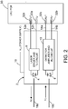
- the receiver has a high-bandwidth detector connected to an amplifier and a receiver (Rx) integrated circuit.
- FIG. 2 is a diagram identifying some features of one example of an SFP transceiver 2 that has been packaged in accordance with the industrial multi-source-agreement (MSA) standard and more specifically is configured to comply with SFP specifications.
- the SFP transceiver 2 is a single-wavelength dual-fiber transceiver that transmits and receives light of the same wavelength ⁇ 1 .
- the term "wavelength" in the context of coherent laser light means the center wavelength of laser light having a narrow spectral width.
- the SFP transceiver 2 partly depicted in FIG. 2 may be ruggedized in accordance with the methodology disclosed in detail below.
- the SFP transceiver 2 includes a laser device 4 and a photodetector 8.
- the laser device 4 can be implemented with single-mode distributed feedback (DFB) lasers, multi-mode Fabry-Perot (FP) lasers or vertical cavity surface-emitting lasers (VCSEL) for high optical output power and low modal noise.
- the photodetector 8 can be implemented with a high-responsivity p-type intrinsic n-type (PIN) photodiode or an avalanche photodiode to provide high receiver sensitivity.
- the SFP transceiver 2 further includes a laser driver and transmit circuit 6 and a detector amplifier and receive circuit 10 which are surface mounted on a double-sided PCB (not shown in FIG. 2 , but see PCB 40 in FIG. 3 ).
- the laser device 4 is driven to emit light of a wavelength ⁇ 1 by the laser driver and transmit circuit 6 in response to receipt of differential transmit signals Tx + and Tx - from an interface PCB 30 of an associated LRU (not shown in FIG. 2 ) via transmit electrical signal lines 12a and 12b respectively.
- the terminals of transmit electrical signal lines 12a and 12b are soldered to respective contact pads 32a formed on the LRU interface PCB 30.
- the laser driver and transmit circuit 6 includes electrical circuitry that converts those differential signals to digital signals representing the data to be transmitted by the laser device 4.
- the photodetector 8 receives light of wavelength ⁇ 1 and converts that detected light into electrical digital signals which are provided to the detector amplifier and receive circuit 10.
- the detector amplifier and receive circuit 10 in turn includes electrical circuitry that converts those electrical digital signals to electrical differential receive signals Rx + and Rx - representing the data received.
- the electrical differential receive signals Rx + and Rx - are transmitted to the LRU interface PCB 30 via receive electrical signal lines 14a and 14b respectively.
- the terminals of receive electrical signal lines 14a and 14b are soldered to respective contact pads 32b formed on the LRU interface PCB 30.
- the laser device 4 is optically coupled to an optical fiber 18a, while the photodetector 8 is optically coupled to an optical fiber 18b.
- Both optical fibers 18a and 18b typically have cores made of the same material having an index of refraction selected to minimize the optical loss for any light of wavelength ⁇ 1 being transmitted along the length of the fiber.
- the SFP transceiver 2 partly depicted in FIG. 2 receives electrical power having a voltage V cc via transceiver power supply line 16.
- FIG. 3 is a block diagram identifying some components of an SFP transceiver 2 that includes a bidirectional optical sub-assembly mounted to a PCB 40.
- the optical sub-assembly includes the laser device 4 and the photodetector 8.
- the laser device 4 may be implemented with a single-mode distributed feedback laser, a multi-mode Fabry-Perot lasers or a vertical cavity surface-emitting laser for high optical output power and low modal noise.
- the photodetector 8 may be implemented with a high-responsivity p-type intrinsic n-type (PIN) photodiode or an avalanche photodiode to provide high receiver sensitivity.
- PIN p-type intrinsic n-type
- the laser device 4 is driven to emit light by a laser driver 42 (surface mounted to PCB 40) in response to receipt at data input terminals 56 of differential transmit signals from an associated line replaceable unit (not shown) via transmit electrical signal lines (not shown in FIG. 3 ).
- the laser driver 42 includes electrical circuitry that converts those electrical differential signals to electrical digital signals representing the data to be transmitted by the laser device 4.
- the photodetector 8 receives light and converts that detected light into electrical signals which are provided to a detector amplifier and receive circuit that includes a transimpedance amplifier 50 that amplifies the detector signal and a limiting amplifier 52 that performs the digitization of the output signal.
- the limiting amplifier 52 converts electrical signals to digital electrical differential receive signals representing the data received.
- the electrical differential receive signals are transmitted to the LRU interface PCB 30 via data output terminals 54 and receive electrical signal lines not shown in FIG. 3 .
- the SFP transceiver 2 depicted in FIG. 3 further includes a pair of LC receptacles 44 and 46 which are sized and configured to receive the termination of a respective optical fiber (not shown in FIG. 3 , but see optical fiber 18 in FIG. 5 ).
- the LC receptacle 44 is positioned so that the termination of an optical fiber inserted therein confronts and is aligned with the laser device 4.
- the optical fiber inside LC receptacle 44 is optically coupled to receive laser pulses from the laser device 4.
- the LC receptacle 46 is positioned so that the termination of an optical fiber inserted therein confronts and is aligned with the photodetector 8.
- the optical fiber inside LC receptacle 44 is optically coupled to emit laser pulses that will impinge on the surface of the photodetector 8 that converts photons into electrons.
- the optical sub-assembly includes two housings (hereinafter "OSA housings").
- OSA housings consists of two integrally formed receptacles, including an LC receptacle that receives a terminated optical fiber and a second receptacle that contains the optical component to be optically coupled to the terminated optical fiber.
- a transmit OSA housing 70 includes the LC receptacle 46 with a first circular cylindrical passageway 96 sized to receive a first end section 92 of a terminus 28 and a transmitter receptacle 74 with a second circular cylindrical passageway 98 (having a diameter greater than the diameter of the first circular cylindrical passageway 96).
- the transmitter receptacle 74 is sized to receive a transistor outline (TO) can 72 that houses the laser device 4.
- the LC receptacle 46 and the transmitter receptacle 74 may be integrally formed or rigidly affixed to each other.
- a detector OSA housing (not shown in FIG. 4 ) includes the LC receptacle 44 integrally formed with a detector receptacle that receives a TO can that houses the photodetector 8.
- the terminus 28 further comprises a main body 90 and a second end section 94.
- the second end section 94 of the terminus 28 has a circular cylindrical cable passageway 76 that receives a jacketed portion of the optical fiber cable 20 depicted in FIG. 5 .
- the main body 90 and first end section 92 of the terminus 28 have a common circular cylindrical fiber passageway 78 that receives an unjacketed portion of the optical fiber 18 of the optical fiber cable 20.
- the OSA housing 70 is made of metallic material (e.g., stainless steel). Terminus 28 may be made of semi-rigid thermoplastic material or metallic material (e.g., stainless steel).
- One commercially available optical fiber cable 20 includes an optical fiber 18 comprising a polymer core and fluorinated polymer cladding and a jacket 86 made of polyethylene. The optical coupling between the photodetector 8 and the associated optical fiber is enabled by an OSA housing and a terminus similar to the sub-assembly depicted in FIG. 4 .
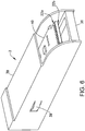
- FIG. 6 is a diagram representing a three-dimensional view of an SFP transceiver 2 that has not been ruggedized.
- the SFP transceiver 2 includes a metal base 36, a PCB 40, various optical and electrical components mounted to the surface of PCB 40 (such as the components identified in FIG. 3 ), and a cover 38.
- the SFP transceiver 2 has two rows 22a and 22b of electrical contact pads 24 on the PCB 40 for making electrical contacts. Each of rows 22a and 22b includes ten contact pads 24. The two rows 22a and 22b of contact pads 24 are located at the back end of the PCB 40.
- the row 22a of contact pads 24 is disposed on a top surface of PCB 40; the row 22b of contact pads 24 is disposed on a bottom surface of PCB 40.
- the non-ruggedized SFP package having 20 contact pads is converted to a 20-pin dual-in-line transceiver package with a pair of alignment pins on the bottom of the package.
- These added features enable the SFP transceiver 2 to be soldered onto an avionics PCB permanently. Additional steps for sealing the SFP transceiver's contact pads, mounting an EMI protection cover on top and installing a pair of alignment metal pins at the bottom of the SFP package are implemented for ruggedizing the SFP transceiver's attachment to the LRU's PCB.
- FIGS. 7-13 are diagrams representing respective three-dimensional views of an SFP transceiver or components thereof at respective stages of a ruggedization process in accordance with one embodiment.
- FIG. 14 is a diagram showing a three-dimensional view of the ruggedized SFP transceiver 1 after completion of the modification process in accordance with one embodiment.
- the reassembled ruggedized SFP transceiver 1 is ready for permanent soldering on a PCB of an avionics LRU, with moisture seal protection (non-conductive moisture sealant 64), metal alignment pins 48a and 48b for vibration protection and a metal cover 80 for EMI protection.
- FIG. 15 is a diagram representing a side view of a ruggedized SFP transceiver 1 soldered to an LRU interface PCB 30 in accordance with one embodiment.
- the distal ends of the two metal alignment pins 48a and 48b and the twenty metal pins 60a and 60b are soldered to the metal LRU interface PCB 30 (the solder is not shown in FIG. 15 ).
- These two metal alignment pins 48a and 40b provide the SFP package alignment for the electrical metal pins 60a and 60b to the printed through holes on the LRU interface PCB 30 and also provide high retention of the SFP package to the LRU interface PCB 30. Therefore, the overall mechanical design of the SFP package has better endurance to high vibration and high humidity.
- the SFP transceiver modification process proposed herein converts the SFP transceiver from a pluggable package to a dual-in-line package which can be reliably soldered onto the PCB of an avionics LRU, with moisture protection seal on the electrical contacts, an EMI protection top cover, and two alignment pins providing mechanical protection for high vibration and extreme temperature cycling.
- the conversion process is very low cost and meets the stringent performance and environmental requirements of avionics systems.
Landscapes
- Physics & Mathematics (AREA)
- General Physics & Mathematics (AREA)
- Optics & Photonics (AREA)
- Engineering & Computer Science (AREA)
- Electromagnetism (AREA)
- Microelectronics & Electronic Packaging (AREA)
- Computer Networks & Wireless Communication (AREA)
- Signal Processing (AREA)
- Manufacturing & Machinery (AREA)
- Optical Couplings Of Light Guides (AREA)
- Insertion, Bundling And Securing Of Wires For Electric Apparatuses (AREA)
- Shielding Devices Or Components To Electric Or Magnetic Fields (AREA)
- Optical Communication System (AREA)
- Small-Scale Networks (AREA)
- Bidirectional Digital Transmission (AREA)
- Communication Control (AREA)
Abstract
Description
- The technology disclosed herein generally relates to optical fiber networks that enable communication between electrical components. In particular, the technology disclosed herein relates to electrical avionics systems interconnected by an optical avionics data bus.
- The use of optical fiber cables instead of electrical wiring for a high-speed avionics data network may result in significant reduction of weight, cost, electromagnetic effects, and complexity of electrical wiring integration. In modern aircraft, line replaceable units (LRUs) (such as avionics computers and sensor units) typically include a housing containing a transceiver to enable optical fiber communication with other LRUs. An optical connector on the LRU housing enables an external optical fiber cable to be connected to the LRU.
- More specifically, each LRU connected to an optical avionics data bus typically includes an optical-electrical media converter) having an electro-optical transmitter and an opto-electrical receiver (hereinafter collectively referred to as an "optical-electrical bidirectional transceiver") to enable optical fiber communication with other LRUs. The electro-optical transmitter converts electrical signals into optical signals; the opto-electrical receiver converts optical signals into electrical signals. An optical connector on a housing of the LRU enables an optical fiber cable to be connected to the LRU.
- In legacy avionics fiber optic systems, non-pluggable small form factor optical-electrical bidirectional transceivers (hereinafter "SFF transceivers") are used inside the LRU of the legacy avionics systems. But the current trend in the optical fiber industry is to gradually discontinue use of non-pluggable SFF transceivers and replace them with small form factor pluggable optical-electrical bidirectional transceivers (hereinafter "SFP transceivers"). As used herein, the term "pluggable", when used as an adjective to characterize a capability of a first component, means that the component may be coupled to and later uncoupled from a second component by inserting male portions (e.g., pins or plugs) of one of the first and second components into respective female portions (e.g., receptacles or sockets) of the other of the first and second components.
- Many modern fiber optic communication system upgrades, new technology and new design features are no longer implemented using SFF transceivers in the industry. Commercially available SFP transceivers have advanced features built-in for modern fiber optic communication systems, including digital diagnostic monitoring and built-in testing. Also because the SFP transceiver is a widely accepted package format in the fiber optic industry, the cost of the SFP transceiver is very low due to the economy of scale. This industrial trend in the development of transceivers creates a problem when deploying new optical fiber systems in avionics platforms. For example, SFP transceivers need to be deployed in many LRUs of these new avionics optical fiber systems.
- Some legacy avionic optical fiber systems use SFF transceivers which have a 10-pin (2 x 5) dual-in-line package format that allows the SFF package to be soldered permanently on the LRU printed circuit board (PCB) without concern for detachment due to vibration. But the currently popular SFP transceiver package has no solder pins and is designed to be pluggable into a 20-pin socket mounted on a PCB. Therefore, the transceiver is not permanently attached to the PCB. While this SFP design is acceptable for use in non-avionics environment, this design is not acceptable for avionics platforms due to concern over detachment of the SFP transceiver under vibration and also corrosion of the SFP transceiver's contact pads due to exposure to moisture and humidity.
- One possible response to the above-described challenge is to fabricate customized SFP transceivers for different avionics platforms using hermetic transceiver packages. This course of action would be expensive. Also finding suppliers capable of making hermetic SFP packages may be challenging because hermetic package format is not part of the multi-source agreement for SFP transceivers in the fiber optic industry. One prior solution for partially ruggedizing an SFP transceiver involved simply depositing a conformal coating on the PCB of the SFP transceiver, but did not include soldering the SFP transceiver to the PCB of an LRU.
- The subject matter disclosed in some detail below includes a method for modifying a low-cost small form factor pluggable optical-electrical bidirectional transceiver (hereinafter "SFP transceiver") to enable ruggedized installation in an avionics system. As used here, the term "ruggedize" means to strengthen a device for better resistance to the effects of vibration or humidity. More specifically, the disclosed subject matter is directed to a method for ruggedizing that converts the SFP transceiver into a dual-in-line package. Such conversion enables the SFP transceiver to be soldered directly on a printed circuit board (PCB) of a line replaceable unit (LRU) of an avionics system, thereby eliminating the concern that the SFP transceiver may become detached due to vibration during aircraft operation. The method also includes a sealing process to protect the contact pads on the SFP transceiver, thereby eliminating any concern that the contact pads could corrode due to long-term moisture and humidity exposure. The method of modification proposed herein converts a pluggable transceiver package to a dual-in-line transceiver package. The product of the method is a ruggedized installation of a SFP transceiver capable of withstanding the rigors of operating in a harsh avionics environment.
- In accordance with some embodiments, the pluggable transceiver package is converted to a dual-in-line transceiver package by soldering a pin header to the contact pads on the PCB of an SFP transceiver and forming a hole in the base of the SFP transceiver for the attached pins to pass through. In one proposed implementation, an SFP transceiver having 20 contact pads is converted to a 20-pin dual-in-line package, which conversion enables the SFP transceiver to be soldered directly on the PCB (e.g., an interface PCB) of an LRU of the avionics system. The method proposed herein also includes a process for sealing the contact pads of the SFP transceiver. In addition, a pair of alignment pins are provided on the SFP package for mechanical support to aid in withstanding the high-vibration avionics environment. A further enhancement is placement of a metal cover on top of the SFP package to protect the SFP transceiver against electromagnetic interference (EMI).
- As used herein, the term "dual-in-line" means that two sets of spaced-apart elements (e.g., metal pins) are arranged along respective lines. Typically the two lines are straight and mutually parallel, although straightness and parallelism are not a requirement provided that the metal pins properly align with contact pads on the LRU PCB.
- The benefits of the methodology proposed herein are manifold: (1) the cost of the rugged SFP transceivers that are needed in advanced avionics fiber optic systems is reduced; (2) the use of expensive hermetic packages for the SFP transceivers is eliminated by sealing the metal contact pads of the SFP transceiver's PCB; (3) the reliability of SFP transceivers used in advanced avionics platforms is enhanced; and (4) EMI protection of the SFP transceivers used in avionics systems is provided.
- Although various embodiments of a method for modifying an SFP transceiver to increase resistance to adverse environmental effects (such as vibration and humidity) will be described in some detail below, one or more of those embodiments may be characterized by one or more of the following aspects.
- One aspect of the subject matter disclosed in detail below is a method for modifying a small form factor pluggable (SFP) transceiver. The method comprises: removing a cover from the SFP transceiver; separating a printed circuit board (PCB) of the SFP transceiver from a metal base of the SFP transceiver; soldering a multiplicity of metal pins to a multiplicity of contact pads on the PCB, the metal pins being held in spaced-apart relationship by a pin holder; forming a feed-through hole in a bottom of the metal base; seating the PCB on the metal base while also seating the pin holder in the feed-through hole; placing a different cover over the PCB; and attaching the different cover to the metal base.
- In accordance with one embodiment of the method described in the immediately preceding paragraph, the different cover is made of a material that provides protection to the PCB against electromagnetic interference. The method in accordance with this embodiment further comprises: depositing non-conductive moisture sealant on the contact pads after soldering; and attaching first and second metal alignment pins to the bottom of the metal base.
- Another aspect of the subject matter disclosed in detail below is a modified small form factor pluggable (SFP) transceiver comprising: a metal base having a bottom with a feed-through hole; a printed circuit board supported by the metal base and having an end with a multiplicity of contact pads; a pin holder comprising a pin holder made of non-electrically conductive material and a multiplicity of metal pins held in spaced-apart relationship by the pin holder; and a cover attached to the metal base, wherein the pin holder is seated in the feed-through hole and the multiplicity of metal pins each have a first portion soldered to a respective contact pad of the multiplicity of contact pads and a second portion that passes through the feed-through hole. The cover is made of a material that provides protection to the PCB against electromagnetic interference.
- In accordance with one embodiment, the modified SFP transceiver described in the immediately preceding paragraph further comprises non-conductive moisture sealant that covers the multiplicity of contact pads and first and second metal alignment pins attached to the bottom of the metal base. In one proposed implementation, the multiplicity of metal pins comprises first and second rows of metal pins, and the multiplicity of contact pads comprises first and second rows of contact pads, the first row of metal pins being soldered to the first row of contact pads, and the second row of metal pins being soldered to the second row of contact pads.
- A further aspect of the subject matter disclosed in detail below is a data transmission system comprising: a fiber optical network; a modified small form factor pluggable (SFP) transceiver optically coupled to the fiber optical network and comprising a multiplicity of contact pads; and an electronic device comprising a first printed circuit board (PCB) having a multiplicity of printed through holes respectively electrically coupled to the multiplicity of contact pads of the modified SFP transceiver. The modified SFP transceiver further comprises: a metal base having a bottom with a feed-through hole; a second printed circuit board (PCB) supported by the metal base and having an end with the multiplicity of contact pads; a pin holder comprising a pin holder made of non-electrically conductive material and a multiplicity of metal pins held in spaced-apart relationship by the pin holder; and a cover attached to the metal base. The pin holder is seated in the feed-through hole and the multiplicity of metal pins each have a first portion soldered to a respective contact pad of the multiplicity of contact pads, a second portion that passes through the feed-through hole and a third portion soldered to a respective printed through hole of the multiplicity of printed through holes.
- In accordance with one embodiment of the data transmission system described in the immediately preceding paragraph, the modified SFP transceiver further comprises non-conductive moisture sealant that covers the multiplicity of contact pads soldered with the multiplicity of metal pins. The modified SFP transceiver also comprises first and second metal alignment pins attached to the bottom of the metal base. The first and second metal alignment pins are soldered to the first PCB of the electronic device. In accordance with one proposed application, the electronic device is a line replaceable unit installed on an aircraft.
- Other aspects of methods for modifying an SFP transceiver to increase resistance to adverse environmental effects are disclosed below.
- The features, functions and advantages discussed in the preceding section may be achieved independently in various embodiments or may be combined in yet other embodiments. Various embodiments will be hereinafter described with reference to drawings for the purpose of illustrating the above-described and other aspects. None of the diagrams briefly described in this section are drawn to scale.
-
FIG. 1 is a diagram representing a three-dimensional cutaway view of a data processing system onboard an aircraft, the data processing system including an optical data communication network. -
FIG. 2 is a block diagram identifying some features of a dual-fiber bidirectional SFP transceiver design in which the transceiver transmits and receives light of the same wavelength. -
FIG. 3 is a block diagram identifying some components of a typical dual-fiber bidirectional SFP transceiver used in some legacy avionics systems. -
FIG. 4 is a diagram representing a sectional view of a terminus/receptacle assembly. -
FIG. 5 is a diagram representing a side view of a portion of an optical fiber cable that may be inserted into the terminus depicted inFIG. 4 for the purpose of optically coupling an optical fiber to an optoelectronic device. -
FIG. 6 is a diagram representing a three-dimensional view of an SFP transceiver that has not been modified in accordance with the method disclosed herein. -
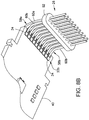
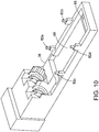
FIGS. 7-13 are diagrams representing respective three-dimensional views of an SFP transceiver or components thereof at respective stages of a modification process in accordance with one embodiment. -
FIG. 14 is a diagram representing a three-dimensional view of a ruggedized SFP transceiver in accordance with one embodiment. -
FIG. 15 is a diagram representing a side view of a ruggedized SFP transceiver soldered to an LRU PCB in accordance with one embodiment. - Reference will hereinafter be made to the drawings in which similar elements in different drawings bear the same reference numerals.
- Illustrative embodiments of methods for modifying an SFP transceiver to increase resistance to adverse environmental effects are described in some detail below. However, not all features of an actual implementation are described in this specification. A person skilled in the art will appreciate that in the development of any such actual embodiment, numerous implementation-specific decisions must be made to achieve the developer's specific goals, such as compliance with system-related and business-related constraints, which will vary from one implementation to another. Moreover, it will be appreciated that such a development effort might be complex and time-consuming, but would nevertheless be a routine undertaking for those of ordinary skill in the art having the benefit of this disclosure.
- Various embodiments of a fiber optical network for enabling optical communication between line replaceable units on an aircraft will be described in detail below for the purpose of illustration. However, implementation of the fiber optical networks disclosed herein is not limited solely to the environment of an aircraft, but rather may be utilized in fiber optical networks onboard other types of vehicles or other types of fiber optical networks (e.g., long-distance terrestrial, data center and fiber-to-the-home/office applications).
- Fiber optical networks have the advantages of higher speed, lower weight and electromagnetic interference immunity over copper wire networks. Many models of commercial aircrafts have fiber optical networks for size, weight and power reduction. It is common practice to connect a number of line replaceable units (LRUs) to each other to achieve communication within an avionics system. For example, a number of LRUs in the forward section of a vehicle (e.g., an aircraft) have been connected to a number of LRUs in the aft section of the vehicle via an avionics data bus.
-
FIG. 1 illustrates anetwork environment 100 comprising anaircraft 102. Anaircraft 102 is an example of a platform in which the connectors disclosed herein may be used. In the example depicted inFIG. 1 , theaircraft 102 hasright wing 104 and aleft wing 106 attached to afuselage 108.Aircraft 102 also includes anengine 110 attached to theright wing 104 and anengine 112 attached to theleft wing 106.Aircraft 102 also has anose section 114 and atail section 116. Thetail section 116 includes a righthorizontal stabilizer 118, a lefthorizontal stabilizer 120, and avertical stabilizer 122. - The
aircraft 102 depicted inFIG. 1 further includes an onboard data communication andprocessing system 124 comprising a fiberoptical network 126 and a plurality ofdevices 127, such as flight deck displays 128,flight control computers 130, and other components, which are connected (and optically coupled) to the fiberoptical network 126. Other types ofdevices 127 may take the form ofLRUs devices 127 use electrical signals internally, so the optical signals transmitted over fiberoptical network 126 are typically converted into electrical signals through the use of optical-electrical media converters (not shown inFIG. 1 ). These optical-electrical media converters (hereinafter "optical-electrical bidirectional transceivers") may be internal or external to the LRU. - In the case of an LRU having one or more optical-electrical transceivers incorporated inside the LRU housing (hereinafter "optical-electrical LRU"), the optical-electrical LRU may be mounted to a rack onboard an aircraft by means of a mechanical assembly that provides support and self-indexing for the LRU. Each optical-electrical LRU contains an internal optical-electrical bidirectional transceiver that is optically coupled to an optical avionics data bus of the fiber
optical network 126 by means of a mating connector that is mechanically coupled to the LRU housing. The mating connector provides the optical connection to aircraft systems and structural support for the LRU. - One type of high-speed (over 1 Gbits/sec) single-wavelength transceiver has one fiber for the transmit (Tx) output optical signal and another fiber for the receive (Rx) input optical signal. The transmitter has a high-speed laser diode connected to a laser driver and transmitter (Tx) integrated circuit. The receiver has a high-bandwidth detector connected to an amplifier and a receiver (Rx) integrated circuit.
-
FIG. 2 is a diagram identifying some features of one example of anSFP transceiver 2 that has been packaged in accordance with the industrial multi-source-agreement (MSA) standard and more specifically is configured to comply with SFP specifications. In this example, theSFP transceiver 2 is a single-wavelength dual-fiber transceiver that transmits and receives light of the same wavelength λ 1. [As used herein, the term "wavelength" in the context of coherent laser light means the center wavelength of laser light having a narrow spectral width.] TheSFP transceiver 2 partly depicted inFIG. 2 may be ruggedized in accordance with the methodology disclosed in detail below. - As seen in
FIG. 2 , theSFP transceiver 2 includes alaser device 4 and aphotodetector 8. Thelaser device 4 can be implemented with single-mode distributed feedback (DFB) lasers, multi-mode Fabry-Perot (FP) lasers or vertical cavity surface-emitting lasers (VCSEL) for high optical output power and low modal noise. Thephotodetector 8 can be implemented with a high-responsivity p-type intrinsic n-type (PIN) photodiode or an avalanche photodiode to provide high receiver sensitivity. TheSFP transceiver 2 further includes a laser driver and transmitcircuit 6 and a detector amplifier and receivecircuit 10 which are surface mounted on a double-sided PCB (not shown inFIG. 2 , but seePCB 40 inFIG. 3 ). - The
laser device 4 is driven to emit light of a wavelength λ 1 by the laser driver and transmitcircuit 6 in response to receipt of differential transmit signals Tx+ and Tx- from aninterface PCB 30 of an associated LRU (not shown inFIG. 2 ) via transmitelectrical signal lines electrical signal lines respective contact pads 32a formed on theLRU interface PCB 30. The laser driver and transmitcircuit 6 includes electrical circuitry that converts those differential signals to digital signals representing the data to be transmitted by thelaser device 4. - Conversely, the
photodetector 8 receives light of wavelength λ 1 and converts that detected light into electrical digital signals which are provided to the detector amplifier and receivecircuit 10. The detector amplifier and receivecircuit 10 in turn includes electrical circuitry that converts those electrical digital signals to electrical differential receive signals Rx+ and Rx- representing the data received. The electrical differential receive signals Rx+ and Rx- are transmitted to theLRU interface PCB 30 via receiveelectrical signal lines electrical signal lines respective contact pads 32b formed on theLRU interface PCB 30. - The
laser device 4 is optically coupled to anoptical fiber 18a, while thephotodetector 8 is optically coupled to anoptical fiber 18b. Bothoptical fibers SFP transceiver 2 partly depicted inFIG. 2 receives electrical power having a voltage Vcc via transceiverpower supply line 16. -
FIG. 3 is a block diagram identifying some components of anSFP transceiver 2 that includes a bidirectional optical sub-assembly mounted to aPCB 40. The optical sub-assembly includes thelaser device 4 and thephotodetector 8. Thelaser device 4 may be implemented with a single-mode distributed feedback laser, a multi-mode Fabry-Perot lasers or a vertical cavity surface-emitting laser for high optical output power and low modal noise. Thephotodetector 8 may be implemented with a high-responsivity p-type intrinsic n-type (PIN) photodiode or an avalanche photodiode to provide high receiver sensitivity. - As depicted in
FIG. 3 , thelaser device 4 is driven to emit light by a laser driver 42 (surface mounted to PCB 40) in response to receipt atdata input terminals 56 of differential transmit signals from an associated line replaceable unit (not shown) via transmit electrical signal lines (not shown inFIG. 3 ). Thelaser driver 42 includes electrical circuitry that converts those electrical differential signals to electrical digital signals representing the data to be transmitted by thelaser device 4. Conversely, thephotodetector 8 receives light and converts that detected light into electrical signals which are provided to a detector amplifier and receive circuit that includes atransimpedance amplifier 50 that amplifies the detector signal and a limitingamplifier 52 that performs the digitization of the output signal. The limitingamplifier 52 converts electrical signals to digital electrical differential receive signals representing the data received. The electrical differential receive signals are transmitted to theLRU interface PCB 30 viadata output terminals 54 and receive electrical signal lines not shown inFIG. 3 . - The
SFP transceiver 2 depicted inFIG. 3 further includes a pair ofLC receptacles FIG. 3 , but seeoptical fiber 18 inFIG. 5 ). TheLC receptacle 44 is positioned so that the termination of an optical fiber inserted therein confronts and is aligned with thelaser device 4. In other words, the optical fiber insideLC receptacle 44 is optically coupled to receive laser pulses from thelaser device 4. Similarly, theLC receptacle 46 is positioned so that the termination of an optical fiber inserted therein confronts and is aligned with thephotodetector 8. In other words, the optical fiber insideLC receptacle 44 is optically coupled to emit laser pulses that will impinge on the surface of thephotodetector 8 that converts photons into electrons. - In addition to the
laser device 4 and photodetector, the optical sub-assembly includes two housings (hereinafter "OSA housings"). Each OSA housing consists of two integrally formed receptacles, including an LC receptacle that receives a terminated optical fiber and a second receptacle that contains the optical component to be optically coupled to the terminated optical fiber. - As seen in the example depicted in
FIG. 4 , a transmitOSA housing 70 includes theLC receptacle 46 with a first circularcylindrical passageway 96 sized to receive afirst end section 92 of aterminus 28 and atransmitter receptacle 74 with a second circular cylindrical passageway 98 (having a diameter greater than the diameter of the first circular cylindrical passageway 96). Thetransmitter receptacle 74 is sized to receive a transistor outline (TO) can 72 that houses thelaser device 4. TheLC receptacle 46 and thetransmitter receptacle 74 may be integrally formed or rigidly affixed to each other. Similarly, a detector OSA housing (not shown inFIG. 4 ) includes theLC receptacle 44 integrally formed with a detector receptacle that receives a TO can that houses thephotodetector 8. - Still referring to
FIG. 4 , theterminus 28 further comprises amain body 90 and asecond end section 94. Thesecond end section 94 of theterminus 28 has a circularcylindrical cable passageway 76 that receives a jacketed portion of theoptical fiber cable 20 depicted inFIG. 5 . Themain body 90 andfirst end section 92 of theterminus 28 have a common circularcylindrical fiber passageway 78 that receives an unjacketed portion of theoptical fiber 18 of theoptical fiber cable 20. Thus, if the portions of theoptical fiber cable 20 shown inFIG. 5 were inserted into theterminus 28 shown in cross section inFIG. 4 , the end face of theoptical fiber 18 would be aligned with and confronting a lens installed in a window (not shown inFIG. 4 ) formed in the TO can 72. This physical arrangement optically couples the laser device 4 (seeFIG. 3 ) to the optical fiber 18 (seeFIG. 5 ). TheOSA housing 70 is made of metallic material (e.g., stainless steel).Terminus 28 may be made of semi-rigid thermoplastic material or metallic material (e.g., stainless steel). One commercially availableoptical fiber cable 20 includes anoptical fiber 18 comprising a polymer core and fluorinated polymer cladding and ajacket 86 made of polyethylene. The optical coupling between thephotodetector 8 and the associated optical fiber is enabled by an OSA housing and a terminus similar to the sub-assembly depicted inFIG. 4 . -
FIG. 6 is a diagram representing a three-dimensional view of anSFP transceiver 2 that has not been ruggedized. TheSFP transceiver 2 includes ametal base 36, aPCB 40, various optical and electrical components mounted to the surface of PCB 40 (such as the components identified inFIG. 3 ), and acover 38. TheSFP transceiver 2 has tworows electrical contact pads 24 on thePCB 40 for making electrical contacts. Each ofrows contact pads 24. The tworows contact pads 24 are located at the back end of thePCB 40. Therow 22a ofcontact pads 24 is disposed on a top surface ofPCB 40; therow 22b ofcontact pads 24 is disposed on a bottom surface ofPCB 40. When theSFP transceiver 2 is plugged into a socket mounted on the PCB of some other device (such as a media converter), electrical contacts are made, thereby communicatively coupling the other device to theSFP transceiver 2. This pluggable feature is good for non-avionic system applications where high vibration and high humidity are not concerns. - In accordance with the ruggedization process disclosed herein, the non-ruggedized SFP package having 20 contact pads is converted to a 20-pin dual-in-line transceiver package with a pair of alignment pins on the bottom of the package. These added features enable the
SFP transceiver 2 to be soldered onto an avionics PCB permanently. Additional steps for sealing the SFP transceiver's contact pads, mounting an EMI protection cover on top and installing a pair of alignment metal pins at the bottom of the SFP package are implemented for ruggedizing the SFP transceiver's attachment to the LRU's PCB. These processes enable low-cost SFP transceivers to be used in harsh avionics environments. -
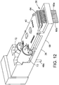
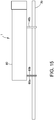
FIGS. 7-13 are diagrams representing respective three-dimensional views of an SFP transceiver or components thereof at respective stages of a ruggedization process in accordance with one embodiment. - (1)
FIG. 6 shows a standard commercial-off-the-shelf (COTS)SFP transceiver 2 before it is disassembled. - (2) To disassemble the
non-ruggedized SFP transceiver 2, two clips 39 (only one of which is visible inFIG. 6 ) on the sides of the transceiver'scover 38 are released and thecover 38 is removed (i.e., separated from the metal base 36). - (3) Following removal of the
cover 38, thePCB 40 ofSFP transceiver 2 is separated from themetal base 36. At the back end of thePCB 40 are tworows electrical contact pads 24, as previously described. The thickness of thePCB 40 is typically around 0.04 inch (40 mils). The size of eachcontact pad 24 is about 0.6 mm by 3.8 mm. - (4)
FIG. 7 is a diagram showing a three-dimensional view of apin header 26 placed near thecontact pads 24 of thePCB 40. Thepin header 26 includes afirst row 58a of ten 90-degree metal pins 60a (hereinafter "metal pins 60a") and asecond row 58b of ten 90-degree metal pins 60b (hereinafter "metal pins 60b"). Thepin header 26 further includes apin holder 62 made of non-conductive material (e.g., plastic). Thepin header 62 has two rows of holes, with ten holes in each row, which receive and hold the vertically disposed portions ofmetal pins metal pins 60a ofrow 58a have a length greater than the length ofmetal pins 60b ofrow 58b by an amount approximately equal to the thickness of thePCB 40. As a result, the horizontally disposed portions ofmetal pins 60a are separated from the horizontally disposed portions ofmetal pins 60b by a gap which is approximately equal to the thickness ofPCB 40, which in this example is 40 mils. The diameter and lateral spacing of the metal pins 60a and 60b match the width and lateral spacing of thecontact pads 24 on thePCB 40. The proximal ends ofmetal pins metal pins metal base 36 is disposed horizontally inFIG. 7 ). - (5) The
pin header 26 is moved from the location depicted inFIG. 7 to a location (shown inFIGS. 8A and8B ) where metal pins 60a ofrow 58a respectively contact (abut)contact pads 24 ofrow 22a andmetal pins 60b ofrow 58a respectively contact (abut)contact pads 24 ofrow 22b. This is accomplished by sliding the horizontally disposed portions of the metal pins 60a and 60b onto the back end of thePCB 40. Then the metal pins 60a ofrow 58a are respectively soldered to contactpads 24 ofrow 22a andmetal pins 60b ofrow 58b are respectively soldered to contactpads 24 ofrow 22b.FIGS. 8A and8B are diagrams showing respective three-dimensional views of thepin header 26 after the metal pins 60a and 60b have been soldered to thecontact pads 24 of thePCB 40. In accordance with one proposed implementation, the metal pins are soldered using an avionics-grade solder alloy (not shown inFIGS. 8A and8B ), such as a gold-tin (AuSn) alloy or a tin-silver (AgSn) alloy which have excellent durability for temperature cycling and vibration. - (6) After soldering the
pin header 26 to thePCB 40, the next step in the transceiver modification process is to deposit a layer ofnon-conductive moisture sealant 64 on the top and bottom surfaces of thecontact pads 24 and abutting portions ofmetal pins FIG. 9 is a diagram showing a three-dimensional view of the pin header/PCB assembly after the deposition ofnon-conductive moisture sealant 64. Thenon-conductive moisture sealant 64 protect themetal contact pads 24 and solder from corrosion in an avionics environment. This sealant can be an epoxy glob top material used in in a standard PCB chip-on-board electronic packaging process, such as the process disclosed by Chan et al. in "High performance, low-cost chip-on-board (COB) FDDI transmitter and receiver for avionics applications," IEEE 1998 Proceedings, 48th Electronic Components and Technology Conference, Seattle, WA, USA, May 25-28, 1998, p. 410. - (7) In addition to the above-described modification of the
PCB 40 of theSFP transceiver 2, themetal base 36 of theSFP transceiver 2 is modified by forming an opening for passage of the vertically disposed portions of the metal pins 60a and 60b.FIG. 10 is a diagram showing a three-dimensional view of themetal base 36 after the formation of a feed-throughhole 66 in the bottom 68 of themetal base 36. The size and shape of the feed-throughhole 66 are designed to match the size and shape of thepin holder 62. Thepin holder 62 is seated in the feed-throughhole 66 when the modifiedPCB 40 and modifiedmetal base 36 are reassembled. Themetal base 36 has foursupport posts 82a-82d which are designed to support thePCB 40 when thePCB 40 andmetal base 36 are assembled. The PCB support posts 82a-82d have specially designed recess slots where thePCB 40 will be seated to enable the PCB's "plugging-in and removal" operation. - (8) After or before the feed-through
hole 66 is formed, two metal alignment pins 48a and 48b are inserted in respective holes formed in the bottom 68 of themetal base 36 by press fitting (or other mechanical process).FIG. 11 is a diagram showing a three-dimensional view of themetal base 36 after the formation of feed-throughhole 66 and after attachment of metal alignment pins 48a and 48b. The two metal alignment pins 48a and 48b aid the alignment of the distal terminations of the metal pins 60a and 60b onto the printed through holes (PTH) of the LRU PCB (not shown inFIG. 11 , but seeLRU interface PCB 30 inFIG. 15 ) during the soldering process. For example, the distal ends of the two metal alignment pins 48a and 48b may be inserted in respective printed through holes formed in the LRU PCB. The two metal alignment pins 48a and 48b are also soldered on two printed through holes on the LRU PCB to prevent detachment of the modified SFP transceiver from the LRU PCB in a high-vibration and shock environment. - (9) After the above-described modifications to the
PCB 40 andmetal base 36, thePCB 40 is reattached to themetal base 36 in a well-known manner. First, thepin header 26 is fed through the feed-throughhole 66 until theplastic pin holder 62 is press fit into the opening. During this movement, thePCB 40 is seated in the PCB support posts 82a-82d. Space grade non-conductive epoxy (not shown in the drawings) is used to securely mount thePCB 40 onto the support posts 82a-82d on themetal base 36.FIG. 12 is a diagram showing a three-dimensional view of themetal base 36 andPCB 40 after reassembly with the metal alignment pins 48a and 48b (two in number) andmetal pins metal base 36. - (10) After the
metal base 36 andPCB 40 have been reassembled, ametal cover 80 placed overPCB 40 and attached tometal base 36, as shown inFIG. 13 . Themetal cover 80 is held on top of the package by means of retaining clips and non-conductive space grade epoxy on the side of metal base 36 (not shown inFIG. 13 ). The result of the above-described modification process is a ruggedized SFP transceiver 1 having dual-in-line metal pins which enable the ruggedized SFP transceiver 1 to be permanently soldered on the PCB of the LRU in an avionics system. Themetal cover 80 provides EMI shielding of the SFP transceiver'sPCB 40. -
FIG. 14 is a diagram showing a three-dimensional view of the ruggedized SFP transceiver 1 after completion of the modification process in accordance with one embodiment. The reassembled ruggedized SFP transceiver 1 is ready for permanent soldering on a PCB of an avionics LRU, with moisture seal protection (non-conductive moisture sealant 64), metal alignment pins 48a and 48b for vibration protection and ametal cover 80 for EMI protection. -
FIG. 15 is a diagram representing a side view of a ruggedized SFP transceiver 1 soldered to anLRU interface PCB 30 in accordance with one embodiment. The distal ends of the two metal alignment pins 48a and 48b and the twentymetal pins FIG. 15 ). These two metal alignment pins 48a and 40b provide the SFP package alignment for theelectrical metal pins LRU interface PCB 30 and also provide high retention of the SFP package to theLRU interface PCB 30. Therefore, the overall mechanical design of the SFP package has better endurance to high vibration and high humidity. - In summary, the SFP transceiver modification process proposed herein converts the SFP transceiver from a pluggable package to a dual-in-line package which can be reliably soldered onto the PCB of an avionics LRU, with moisture protection seal on the electrical contacts, an EMI protection top cover, and two alignment pins providing mechanical protection for high vibration and extreme temperature cycling. The conversion process is very low cost and meets the stringent performance and environmental requirements of avionics systems.
- While methods for modifying an SFP transceiver to increase resistance to adverse environmental effects have been described with reference to various embodiments, it will be understood by those skilled in the art that various changes may be made and equivalents may be substituted for elements thereof without departing from the teachings herein. In addition, many modifications may be made to adapt the concepts and reductions to practice disclosed herein to a particular situation. Accordingly, it is intended that the subject matter covered by the claims not be limited to the disclosed embodiments.
- Further, the disclosure comprises examples according to the following clauses:
- Clause 1. A method for modifying a small form factor pluggable (SFP) transceiver, the method comprising: removing a cover from the SFP transceiver; separating a printed circuit board (PCB) of the SFP transceiver from a metal base of the SFP transceiver; soldering a multiplicity of metal pins to a multiplicity of contact pads on the PCB, the metal pins being held in spaced-apart relationship by a pin holder; forming a feed-through hole in a bottom of the metal base; seating the PCB on the metal base while also seating the pin holder in the feed-through hole; placing a different cover over the PCB; and attaching the different cover to the metal base.
-
Clause 2. The method as recited in Clause 1, wherein the different cover is made of a material that provides protection to the PCB against electromagnetic interference. - Clause 3. The method as recited in
Clause 1 or 2, further comprising depositing non-conductive moisture sealant on the contact pads after soldering. -
Clause 4. The method as recited in any one of Clauses 1 to 3, wherein the multiplicity of metal pins comprises first and second rows of metal pins, and the multiplicity of contact pads comprises first and second rows of contact pads, the first row of metal pins being soldered to the first row of contact pads, and the second row of metal pins being soldered to the second row of contact pads. - Clause 5. The method as recited in
Clause 4, wherein the first row of contact pads is disposed on a top surface of the PCB and the second row of contact pads is disposed on a bottom surface of the PCB. -
Clause 6. The method as recited inClause 4 or 5, wherein distal terminations of the multiplicity of metal pins are coplanar. - Clause 7. The method as recited in
Clause 6, further comprising soldering the distal terminations of the multiplicity of metal pins to a PCB of a line replaceable unit onboard an aircraft. -
Clause 8. The method as recited in any one of Clauses 1 to 7, further comprising attaching first and second metal alignment pins to the bottom of the metal base. - Clause 9. The method as recited in
Clause 8, further comprising soldering distal terminations of the multiplicity of metal pins and distal ends of the first and second metal alignment pins to a PCB of a line replaceable unit onboard an aircraft. -
Clause 10. A modified small form factor pluggable (SFP) transceiver comprising: a metal base having a bottom with a feed-through hole; a printed circuit board (PCB) supported by the metal base and having an end with a multiplicity of contact pads; a pin header comprising a pin holder made of non-electrically conductive material and a multiplicity of metal pins held in spaced-apart relationship by the pin holder; and a cover attached to the metal base, wherein the pin holder is seated in the feed-through hole and the multiplicity of metal pins each have a first portion soldered to a respective contact pad of the multiplicity of contact pads and a second portion that passes through the feed-through hole. - Clause 11. The modified SFP transceiver as recited in
Clause 10, wherein the cover is made of a material that provides protection to the PCB against electromagnetic interference. - Clause 12. The modified SFP transceiver as recited in
Clause 10 or 11, further comprising non-conductive moisture sealant that covers the multiplicity of contact pads. - Clause 13. The modified SFP transceiver as recited in any one of
Clauses 10 to 12, wherein the multiplicity of metal pins comprises first and second rows of metal pins, and the multiplicity of contact pads comprises first and second rows of contact pads, the first row of metal pins being soldered to the first row of contact pads, and the second row of metal pins being soldered to the second row of contact pads. - Clause 14. The modified SFP transceiver as recited in Clause 13, wherein the first row of contact pads is disposed on a top surface of the PCB and the second row of contact pads is disposed on a bottom surface of the PCB.
- Clause 15. The modified SFP transceiver as recited in Clause 13 or 14, wherein distal terminations of the multiplicity of metal pins are coplanar.
-
Clause 16. The modified SFP transceiver as recited in any one ofClauses 10 to 15, further comprising first and second metal alignment pins attached to the bottom of the metal base. - Clause 17. A data transmission system comprising: a fiber optical network; the modified SFP transceiver of any one of
Clauses 10 to 16 optically coupled to the fiber optical network and comprising a multiplicity of contact pads, wherein the PCB of the modified SFP transceiver is a second printed circuit board (PCB) supported by the metal base and having an end with the multiplicity of contact pads; and an electronic device comprising a first printed circuit board (PCB) having a multiplicity of printed through holes respectively electrically coupled to the multiplicity of contact pads of the modified SFP transceiver. -
Clause 18. A data transmission system comprising: a fiber optical network; a modified small form factor pluggable (SFP) transceiver optically coupled to the fiber optical network and comprising a multiplicity of contact pads; and an electronic device comprising a first printed circuit board (PCB) having a multiplicity of printed through holes respectively electrically coupled to the multiplicity of contact pads of the modified SFP transceiver, wherein the modified SFP transceiver further comprises: a metal base having a bottom with a feed-through hole; a second printed circuit board (PCB) supported by the metal base and having an end with the multiplicity of contact pads; a pin header comprising a pin holder made of non-electrically conductive material and a multiplicity of metal pins held in spaced-apart relationship by the pin holder; and a cover attached to the metal base, wherein the pin holder is seated in the feed-through hole and the multiplicity of metal pins each have a first portion soldered to a respective contact pad of the multiplicity of contact pads, a second portion that passes through the feed-through hole and a third portion soldered to a respective printed through hole of the multiplicity of printed through holes. - Clause 19. The data transmission system as recited in
Clause 17 or 18, wherein the modified SFP transceiver further comprises non-conductive moisture sealant that covers the multiplicity of contact pads soldered with the multiplicity of metal pins. -
Clause 20. The data transmission system as recited in any one of Clauses 17 to 19, wherein the modified SFP transceiver further comprises first and second metal alignment pins attached to the bottom of the metal base, wherein the first and second metal alignment pins are soldered to the first PCB of the electronic device. - Clause 21. The data transmission system as recited in any one of Clauses 17 to 20, wherein the electronic device is a line replaceable unit installed on an aircraft.
- The method claims set forth hereinafter should not be construed to require that the steps recited therein be performed in alphabetical order (any alphabetical ordering in the claims is used solely for the purpose of referencing previously recited steps) or in the order in which they are recited unless the claim language explicitly specifies or states conditions indicating a particular order in which some or all of those steps are performed. Nor should the method claims be construed to exclude any portions of two or more steps being performed concurrently or alternatingly unless the claim language explicitly states a condition that precludes such an interpretation.
Claims (15)
- A method for modifying a small form factor pluggable (SFP) transceiver (2), the method comprising:removing a cover (38) from the SFP transceiver (2);separating a printed circuit board (PCB) (40) of the SFP transceiver (2) from a metal base (36) of the SFP transceiver (2);soldering a multiplicity of metal pins (60a, 60b) to a multiplicity of contact pads (24) on the PCB (40), the metal pins (60a, 60b) being held in spaced-apart relationship by a pin holder (62);forming a feed-through hole (66) in a bottom (68) of the metal base (36);seating the PCB (40) on the metal base (36) while also seating the pin holder (62) in the feed-through hole (66);placing a different cover (80) over the PCB (40), preferably wherein the different cover (80) is made of a material that provides protection to the PCB (40) against electromagnetic interference; andattaching the different cover (80) to the metal base (36).
- The method as recited in claim 1, further comprising depositing non-conductive moisture sealant (64) on the contact pads (24) after soldering.
- The method as recited in claim 1 or 2, wherein the multiplicity of metal pins (60a, 60b) comprises first and second rows (58a, 58b) of metal pins, and the multiplicity of contact pads (24) comprises first and second rows (22a, 22b) of contact pads, the first row (58a) of metal pins being soldered to the first row (22a) of contact pads, and the second row (58b) of metal pins being soldered to the second row (22b) of contact pads,
preferably wherein the first row (22a) of contact pads is disposed on a top surface of the PCB (40) and the second row (22b) of contact pads is disposed on a bottom surface of the PCB (40). - The method as recited in claim 3, further comprising soldering the distal terminations of the multiplicity of metal pins (60a, 60b) to a PCB (30) of a line replaceable unit onboard an aircraft (102).
- The method as recited in any one of claims 1 to 4, further comprising attaching first and second metal alignment pins (48a, 48b) to the bottom (68) of the metal base (36).
- The method as recited in claim 5, further comprising soldering distal terminations of the multiplicity of metal pins (60a, 60b) and distal ends of the first and second metal alignment pins (48a, 48b) to a PCB (30) of a line replaceable unit onboard an aircraft (102).
- A modified small form factor pluggable (SFP) transceiver (2) comprising:a metal base (36) having a bottom (68) with a feed-through hole (66);a printed circuit board (PCB) (40) supported by the metal base (36) and having an end with a multiplicity of contact pads (24);a pin header (26) comprising a pin holder (62) made of non-electrically conductive material and a multiplicity of metal pins (60a, 60b) held in spaced-apart relationship by the pin holder (62); anda cover (80) attached to the metal base (36),wherein the pin holder (62) is seated in the feed-through hole (66) and the multiplicity of metal pins (60a, 60b) each have a first portion soldered to a respective contact pad of the multiplicity of contact pads (24) and a second portion that passes through the feed-through hole (66).
- The modified SFP transceiver (2) as recited in claim 7, wherein the cover (80) is made of a material that provides protection to the PCB (40) against electromagnetic interference.
- The modified SFP transceiver (2) as recited in claim 7 or 8, further comprising non-conductive moisture sealant (64) that covers the multiplicity of contact pads (24).
- The modified SFP transceiver (2) as recited in any one of claims 7 to 9, wherein the multiplicity of metal pins (60a, 60b) comprises first and second rows (58a, 58b) of metal pins, and the multiplicity of contact pads (24) comprises first and second rows (22a, 22b) of contact pads, the first row (58s) of metal pins being soldered to the first row (22a) of contact pads, and the second row (58b) of metal pins being soldered to the second row (22b) of contact pads,
preferably wherein distal terminations of the multiplicity of metal pins (60a, 60b) are coplanar. - The modified SFP transceiver (2) as recited in any one of claims 7 to 10, further comprising first and second metal alignment pins (48a, 48b) attached to the bottom (68) of the metal base (36).
- A data transmission system (124) comprising:a fiber optical network (126);the modified SFP transceiver (2) of any one claims 7 to 11 optically coupled to the fiber optical network (126); andan electronic device (132) comprising a first printed circuit board (PCB) (30) having a multiplicity of printed through holes respectively electrically coupled to the multiplicity of contact pads (24) of the modified SFP transceiver (2),wherein the PCB (40) of the modified SFP transceiver (2) is a second printed circuit board (PCB) supported by the metal base (36) and having an end with the multiplicity of contact pads (24).
- The data transmission system (124) as recited in claim 12, wherein the modified SFP transceiver (2) further comprises non-conductive moisture sealant (64) that covers the multiplicity of contact pads (24) soldered with the multiplicity of metal pins (60a, 60b).
- The data transmission system (124) as recited in claim 12 or 13, wherein the modified SFP transceiver (2) further comprises first and second metal alignment pins (48a, 48b) attached to the bottom (68) of the metal base (36), wherein the first and second metal alignment pins (48a, 48b) are soldered to the first PCB (30) of the electronic device (132).
- The data transmission system (124) as recited in any one of claims 12 to 14, wherein the electronic device (132) is a line replaceable unit installed on an aircraft (102).
Applications Claiming Priority (1)
| Application Number | Priority Date | Filing Date | Title |
|---|---|---|---|
| US16/391,136 US10754111B1 (en) | 2019-04-22 | 2019-04-22 | Method for modifying small form factor pluggable transceiver for avionics applications |
Publications (2)
| Publication Number | Publication Date |
|---|---|
| EP3731608A1 true EP3731608A1 (en) | 2020-10-28 |
| EP3731608B1 EP3731608B1 (en) | 2023-08-16 |
Family
ID=69374156
Family Applications (1)
| Application Number | Title | Priority Date | Filing Date |
|---|---|---|---|
| EP20153964.0A Active EP3731608B1 (en) | 2019-04-22 | 2020-01-28 | Method for modifying small form factor pluggable transceiver for avionics applications and small factor pluggable transceiver for avionics applications |
Country Status (5)
| Country | Link |
|---|---|
| US (1) | US10754111B1 (en) |
| EP (1) | EP3731608B1 (en) |
| JP (1) | JP7534117B2 (en) |
| CN (1) | CN111830643B (en) |
| TW (1) | TWI824105B (en) |
Families Citing this family (3)
| Publication number | Priority date | Publication date | Assignee | Title |
|---|---|---|---|---|
| US11039202B2 (en) * | 2019-05-08 | 2021-06-15 | Artilux, Inc. | HDMI apparatus using optical communication |
| WO2022148183A1 (en) * | 2021-01-08 | 2022-07-14 | 青岛海信宽带多媒体技术有限公司 | Optical module |
| CN115395256A (en) * | 2022-09-22 | 2022-11-25 | 宁波志伦电子有限公司 | Photoelectric female seat with power connector |
Citations (5)
| Publication number | Priority date | Publication date | Assignee | Title |
|---|---|---|---|---|
| US5666721A (en) * | 1994-01-18 | 1997-09-16 | Matsushita Electric Industrial Co., Ltd. | Method of soldering an electronic connector on a printed circuit board |
| US5713126A (en) * | 1993-12-24 | 1998-02-03 | Matsushita Electric Industrial Co., Ltd. | Method of mounting electronic connector on an end of printed circuit board |
| US6790051B1 (en) * | 2003-12-20 | 2004-09-14 | Lear Corporation | Connector for printed circuit board |
| DE102007039064A1 (en) * | 2007-08-17 | 2009-02-19 | Robert Buck | Electronic device for use as control device for pump, has plug connector with two connector pins and contact holder holding connector pins and connector pin is arranged above and below printed circuit board |
| CN102377077A (en) * | 2010-08-16 | 2012-03-14 | 富士康(昆山)电脑接插件有限公司 | Connector and component thereof |
Family Cites Families (41)
| Publication number | Priority date | Publication date | Assignee | Title |
|---|---|---|---|---|
| US5317440A (en) * | 1990-05-21 | 1994-05-31 | Hughes Aircraft Company | Single wavelength bidirectional optical fiber communication link |
| CA2161915A1 (en) * | 1994-11-02 | 1996-05-03 | Sosaku Sawada | Optical module circuit board having flexible structure |
| US20040069997A1 (en) * | 1999-05-27 | 2004-04-15 | Edwin Dair | Method and apparatus for multiboard fiber optic modules and fiber optic module arrays |
| US20010030789A1 (en) * | 1999-05-27 | 2001-10-18 | Wenbin Jiang | Method and apparatus for fiber optic modules |
| AU2573401A (en) * | 1999-11-01 | 2001-05-14 | Cielo Communications, Inc. | Optical device using chip-on-board technology |
| US6416238B1 (en) * | 2000-08-07 | 2002-07-09 | Stratos Lightwave, Inc. | Modular high density multiple optical transmitter/receiver array |
| US7079775B2 (en) * | 2001-02-05 | 2006-07-18 | Finisar Corporation | Integrated memory mapped controller circuit for fiber optics transceiver |
| US6659655B2 (en) * | 2001-02-12 | 2003-12-09 | E20 Communications, Inc. | Fiber-optic modules with housing/shielding |
| US6607308B2 (en) * | 2001-02-12 | 2003-08-19 | E20 Communications, Inc. | Fiber-optic modules with shielded housing/covers having mixed finger types |
| JP3803264B2 (en) | 2001-05-29 | 2006-08-02 | 株式会社フジクラ | Optical transceiver and method for manufacturing optical transceiver |
| TW504596B (en) * | 2001-06-28 | 2002-10-01 | Sampo Corp | Transceiver module with a clip used in an optical fiber communications system |
| JP4019674B2 (en) * | 2001-09-28 | 2007-12-12 | 住友電気工業株式会社 | Optical module |
| US6869231B2 (en) * | 2002-05-01 | 2005-03-22 | Jds Uniphase Corporation | Transmitters, receivers, and transceivers including an optical bench |
| US7130194B2 (en) | 2002-10-31 | 2006-10-31 | Finisar Corporation | Multi-board optical transceiver |
| US7717627B2 (en) * | 2003-12-29 | 2010-05-18 | Finisar Corporation | Electrical component connector with misalignment compensation |
| US7350979B2 (en) * | 2004-02-13 | 2008-04-01 | Sumitomo Electric Industries, Ltd. | Optical transceiver having an optical receptacle optionally fixed to a frame |
| JP2005311363A (en) * | 2004-04-20 | 2005-11-04 | Sumitomo Electric Ind Ltd | Optical assembly with increased electrostatic breakdown voltage |
| JP2005316475A (en) * | 2004-04-29 | 2005-11-10 | Sumitomo Electric Ind Ltd | Optical transceiver |
| US7280724B2 (en) * | 2004-06-16 | 2007-10-09 | Sumitomo Electric Industries, Ltd. | Optical subassembly and optical transceiver installing the same |
| US7125261B2 (en) * | 2004-10-05 | 2006-10-24 | Sumitomo Electric Industries, Ltd. | Optical transceiver with a pluggable function |
| US7406230B2 (en) * | 2004-10-05 | 2008-07-29 | Sumitomo Electric Industries, Ltd. | Optical transceiver with a pluggable function |
| US7603097B2 (en) * | 2004-12-30 | 2009-10-13 | Valeo Radar Systems, Inc. | Vehicle radar sensor assembly |
| US7367720B2 (en) * | 2005-03-15 | 2008-05-06 | Sumitomo Electric Industries, Ltd. | Optical transceiver with optical subassemblies optionally fixed to housing |
| US7563035B2 (en) * | 2005-04-29 | 2009-07-21 | Finisar Corporation | Connector for box optical subassembly |
| FR2890275B1 (en) | 2005-08-31 | 2008-12-19 | Airbus France Sas | OPTICAL COMMUNICATION BUS NETWORK FOR AVIONICS EQUIPMENT |
| US7359592B2 (en) * | 2006-03-21 | 2008-04-15 | The Boeing Company | Single fiber links for full duplex aircraft data network |
| US20080056647A1 (en) * | 2006-08-31 | 2008-03-06 | Mark Margolin | Active modular optoelectronic components |
| US7785020B2 (en) * | 2007-07-06 | 2010-08-31 | Finisar Corporation | Optical component and transceiver packaging |
| US7965913B2 (en) * | 2008-04-11 | 2011-06-21 | The Boeing Company | Optical star coupler |
| US8721193B2 (en) | 2010-08-13 | 2014-05-13 | Finisar Corporation | Electronic module having multiple flex circuit connectors |
| US8611755B2 (en) * | 2011-01-27 | 2013-12-17 | Avago Technologies General Ip (Singapore) Pte. Ltd. | Optical transmitter with hybridly integrated driver |
| US8554032B2 (en) * | 2011-12-12 | 2013-10-08 | The Boeing Company | Optical star coupler for plastic optical fibers |
| US20140049292A1 (en) * | 2012-08-17 | 2014-02-20 | Ati Technologies Ulc | Integrated circuit package having medium-independent signaling interface coupled to connector assembly |
| US20160085027A1 (en) * | 2013-07-30 | 2016-03-24 | The Boeing Company | Tapered optical mixing rods |
| US10564357B2 (en) * | 2013-07-30 | 2020-02-18 | The Boeing Company | Plastic optical fiber bus network using tapered mixing rods |
| US9791644B2 (en) * | 2014-11-05 | 2017-10-17 | The Boeing Company | Data bus-in-a-box (BiB) system design and implementation |
| US9438338B1 (en) * | 2015-04-13 | 2016-09-06 | The Boeing Company | System for bidirectional free-space laser communication of gigabit Ethernet telemetry data |
| CN106468809B (en) * | 2015-08-19 | 2020-01-03 | 乾坤科技股份有限公司 | Optoelectronic module and method for manufacturing the same |
| US9869837B2 (en) * | 2015-12-08 | 2018-01-16 | Te Connectivity Corporation | Heat dissipating communication system |
| US9778419B1 (en) * | 2016-06-23 | 2017-10-03 | The Boeing Company | Fiber optical system with fiber end face area relationships |
| TWI647501B (en) * | 2016-12-13 | 2019-01-11 | 峰川光電股份有限公司 | Method for manufacturing active optical cable |
-
2019
- 2019-04-22 US US16/391,136 patent/US10754111B1/en active Active
-
2020
- 2020-01-28 EP EP20153964.0A patent/EP3731608B1/en active Active
- 2020-01-30 TW TW109102890A patent/TWI824105B/en active
- 2020-03-09 CN CN202010155852.3A patent/CN111830643B/en active Active
- 2020-04-09 JP JP2020070477A patent/JP7534117B2/en active Active
Patent Citations (5)
| Publication number | Priority date | Publication date | Assignee | Title |
|---|---|---|---|---|
| US5713126A (en) * | 1993-12-24 | 1998-02-03 | Matsushita Electric Industrial Co., Ltd. | Method of mounting electronic connector on an end of printed circuit board |
| US5666721A (en) * | 1994-01-18 | 1997-09-16 | Matsushita Electric Industrial Co., Ltd. | Method of soldering an electronic connector on a printed circuit board |
| US6790051B1 (en) * | 2003-12-20 | 2004-09-14 | Lear Corporation | Connector for printed circuit board |
| DE102007039064A1 (en) * | 2007-08-17 | 2009-02-19 | Robert Buck | Electronic device for use as control device for pump, has plug connector with two connector pins and contact holder holding connector pins and connector pin is arranged above and below printed circuit board |
| CN102377077A (en) * | 2010-08-16 | 2012-03-14 | 富士康(昆山)电脑接插件有限公司 | Connector and component thereof |
Non-Patent Citations (1)
| Title |
|---|
| CHAN ET AL.: "High performance, low-cost chip-on-board (COB) FDDI transmitter and receiver for avionics applications", IEEE 1998 PROCEEDINGS, 48TH ELECTRONIC COMPONENTS AND TECHNOLOGY CONFERENCE, 25 May 1998 (1998-05-25), pages 410, XP010283734, DOI: 10.1109/ECTC.1998.678726 |
Also Published As
| Publication number | Publication date |
|---|---|
| TW202045969A (en) | 2020-12-16 |
| JP2020194958A (en) | 2020-12-03 |
| EP3731608B1 (en) | 2023-08-16 |
| US10754111B1 (en) | 2020-08-25 |
| JP7534117B2 (en) | 2024-08-14 |
| CN111830643B (en) | 2023-06-06 |
| CN111830643A (en) | 2020-10-27 |
| TWI824105B (en) | 2023-12-01 |
Similar Documents
| Publication | Publication Date | Title |
|---|---|---|
| TWI830793B (en) | Avionics pluggable active optical connector | |
| CN110582712B (en) | Fiber Optic Modules with Integrated Lenses | |
| US8195017B2 (en) | Consumer input/output (CIO) optical transceiver module for use in an active optical cable, an active optical cable that incorporates the CIO optical transceiver module, and a method | |
| CN103293607B (en) | Pluggable optical transceiver | |
| US7690849B2 (en) | Fiber optic connector, active contact inserts therefor, and associated methods | |
| US8740476B2 (en) | Connectored cable and method for manufacturing connectored cable | |
| US10574359B2 (en) | Single-wavelength bidirectional transceiver with integrated optical fiber coupler | |
| EP3731608B1 (en) | Method for modifying small form factor pluggable transceiver for avionics applications and small factor pluggable transceiver for avionics applications | |
| EP3229053A1 (en) | Optical module | |
| US20190346637A1 (en) | Optoelectronic optical-link module, integrating a device for removably mounting an optical contact element, associated method for toolessly demounting/demounting | |
| US10101537B2 (en) | High-speed data connector | |
| US8636426B2 (en) | Photoelectric conversion system with optical transceive module | |
| US10310200B1 (en) | Optical transmission module and optical transmission apparatus |
Legal Events
| Date | Code | Title | Description |
|---|---|---|---|
| PUAI | Public reference made under article 153(3) epc to a published international application that has entered the european phase |
Free format text: ORIGINAL CODE: 0009012 |
|
| STAA | Information on the status of an ep patent application or granted ep patent |
Free format text: STATUS: THE APPLICATION HAS BEEN PUBLISHED |
|
| AK | Designated contracting states |
Kind code of ref document: A1 Designated state(s): AL AT BE BG CH CY CZ DE DK EE ES FI FR GB GR HR HU IE IS IT LI LT LU LV MC MK MT NL NO PL PT RO RS SE SI SK SM TR |
|
| AX | Request for extension of the european patent |
Extension state: BA ME |
|
| STAA | Information on the status of an ep patent application or granted ep patent |
Free format text: STATUS: REQUEST FOR EXAMINATION WAS MADE |
|
| 17P | Request for examination filed |
Effective date: 20210423 |
|
| RBV | Designated contracting states (corrected) |
Designated state(s): AL AT BE BG CH CY CZ DE DK EE ES FI FR GB GR HR HU IE IS IT LI LT LU LV MC MK MT NL NO PL PT RO RS SE SI SK SM TR |
|
| RIN1 | Information on inventor provided before grant (corrected) |
Inventor name: CHAN, ERIC YUEN-JUN Inventor name: KOSHINZ, DENNIS G. |
|
| STAA | Information on the status of an ep patent application or granted ep patent |
Free format text: STATUS: EXAMINATION IS IN PROGRESS |
|
| 17Q | First examination report despatched |
Effective date: 20221214 |
|
| REG | Reference to a national code |
Ref country code: DE Ref legal event code: R079 Free format text: PREVIOUS MAIN CLASS: H05K0005020000 Ipc: G02B0006420000 Ref country code: DE Ref legal event code: R079 Ref document number: 602020015654 Country of ref document: DE Free format text: PREVIOUS MAIN CLASS: H05K0005020000 Ipc: G02B0006420000 |
|
| GRAP | Despatch of communication of intention to grant a patent |
Free format text: ORIGINAL CODE: EPIDOSNIGR1 |
|
| STAA | Information on the status of an ep patent application or granted ep patent |
Free format text: STATUS: GRANT OF PATENT IS INTENDED |
|
| RIC1 | Information provided on ipc code assigned before grant |
Ipc: H04B 10/40 20130101ALI20230209BHEP Ipc: H05K 1/11 20060101ALI20230209BHEP Ipc: H05K 3/34 20060101ALI20230209BHEP Ipc: H01R 12/57 20110101ALI20230209BHEP Ipc: H01R 4/02 20060101ALI20230209BHEP Ipc: G02B 6/42 20060101AFI20230209BHEP |
|
| RAP3 | Party data changed (applicant data changed or rights of an application transferred) |
Owner name: THE BOEING COMPANY |
|
| INTG | Intention to grant announced |
Effective date: 20230228 |
|
| GRAS | Grant fee paid |
Free format text: ORIGINAL CODE: EPIDOSNIGR3 |
|
| GRAA | (expected) grant |
Free format text: ORIGINAL CODE: 0009210 |
|
| STAA | Information on the status of an ep patent application or granted ep patent |
Free format text: STATUS: THE PATENT HAS BEEN GRANTED |
|
| AK | Designated contracting states |
Kind code of ref document: B1 Designated state(s): AL AT BE BG CH CY CZ DE DK EE ES FI FR GB GR HR HU IE IS IT LI LT LU LV MC MK MT NL NO PL PT RO RS SE SI SK SM TR |
|
| REG | Reference to a national code |
Ref country code: CH Ref legal event code: EP Ref country code: DE Ref legal event code: R096 Ref document number: 602020015654 Country of ref document: DE |
|
| P01 | Opt-out of the competence of the unified patent court (upc) registered |
Effective date: 20230728 |
|
| REG | Reference to a national code |
Ref country code: IE Ref legal event code: FG4D |
|
| REG | Reference to a national code |
Ref country code: LT Ref legal event code: MG9D |
|
| REG | Reference to a national code |
Ref country code: NL Ref legal event code: MP Effective date: 20230816 |
|
| REG | Reference to a national code |
Ref country code: AT Ref legal event code: MK05 Ref document number: 1600605 Country of ref document: AT Kind code of ref document: T Effective date: 20230816 |
|
| PG25 | Lapsed in a contracting state [announced via postgrant information from national office to epo] |
Ref country code: GR Free format text: LAPSE BECAUSE OF FAILURE TO SUBMIT A TRANSLATION OF THE DESCRIPTION OR TO PAY THE FEE WITHIN THE PRESCRIBED TIME-LIMIT Effective date: 20231117 |
|
| PG25 | Lapsed in a contracting state [announced via postgrant information from national office to epo] |
Ref country code: IS Free format text: LAPSE BECAUSE OF FAILURE TO SUBMIT A TRANSLATION OF THE DESCRIPTION OR TO PAY THE FEE WITHIN THE PRESCRIBED TIME-LIMIT Effective date: 20231216 |
|
| PG25 | Lapsed in a contracting state [announced via postgrant information from national office to epo] |
Ref country code: SE Free format text: LAPSE BECAUSE OF FAILURE TO SUBMIT A TRANSLATION OF THE DESCRIPTION OR TO PAY THE FEE WITHIN THE PRESCRIBED TIME-LIMIT Effective date: 20230816 Ref country code: RS Free format text: LAPSE BECAUSE OF FAILURE TO SUBMIT A TRANSLATION OF THE DESCRIPTION OR TO PAY THE FEE WITHIN THE PRESCRIBED TIME-LIMIT Effective date: 20230816 Ref country code: PT Free format text: LAPSE BECAUSE OF FAILURE TO SUBMIT A TRANSLATION OF THE DESCRIPTION OR TO PAY THE FEE WITHIN THE PRESCRIBED TIME-LIMIT Effective date: 20231218 Ref country code: NO Free format text: LAPSE BECAUSE OF FAILURE TO SUBMIT A TRANSLATION OF THE DESCRIPTION OR TO PAY THE FEE WITHIN THE PRESCRIBED TIME-LIMIT Effective date: 20231116 Ref country code: NL Free format text: LAPSE BECAUSE OF FAILURE TO SUBMIT A TRANSLATION OF THE DESCRIPTION OR TO PAY THE FEE WITHIN THE PRESCRIBED TIME-LIMIT Effective date: 20230816 Ref country code: LV Free format text: LAPSE BECAUSE OF FAILURE TO SUBMIT A TRANSLATION OF THE DESCRIPTION OR TO PAY THE FEE WITHIN THE PRESCRIBED TIME-LIMIT Effective date: 20230816 Ref country code: LT Free format text: LAPSE BECAUSE OF FAILURE TO SUBMIT A TRANSLATION OF THE DESCRIPTION OR TO PAY THE FEE WITHIN THE PRESCRIBED TIME-LIMIT Effective date: 20230816 Ref country code: IS Free format text: LAPSE BECAUSE OF FAILURE TO SUBMIT A TRANSLATION OF THE DESCRIPTION OR TO PAY THE FEE WITHIN THE PRESCRIBED TIME-LIMIT Effective date: 20231216 Ref country code: HR Free format text: LAPSE BECAUSE OF FAILURE TO SUBMIT A TRANSLATION OF THE DESCRIPTION OR TO PAY THE FEE WITHIN THE PRESCRIBED TIME-LIMIT Effective date: 20230816 Ref country code: GR Free format text: LAPSE BECAUSE OF FAILURE TO SUBMIT A TRANSLATION OF THE DESCRIPTION OR TO PAY THE FEE WITHIN THE PRESCRIBED TIME-LIMIT Effective date: 20231117 Ref country code: FI Free format text: LAPSE BECAUSE OF FAILURE TO SUBMIT A TRANSLATION OF THE DESCRIPTION OR TO PAY THE FEE WITHIN THE PRESCRIBED TIME-LIMIT Effective date: 20230816 Ref country code: AT Free format text: LAPSE BECAUSE OF FAILURE TO SUBMIT A TRANSLATION OF THE DESCRIPTION OR TO PAY THE FEE WITHIN THE PRESCRIBED TIME-LIMIT Effective date: 20230816 |
|
| PG25 | Lapsed in a contracting state [announced via postgrant information from national office to epo] |
Ref country code: PL Free format text: LAPSE BECAUSE OF FAILURE TO SUBMIT A TRANSLATION OF THE DESCRIPTION OR TO PAY THE FEE WITHIN THE PRESCRIBED TIME-LIMIT Effective date: 20230816 |
|
| PG25 | Lapsed in a contracting state [announced via postgrant information from national office to epo] |
Ref country code: ES Free format text: LAPSE BECAUSE OF FAILURE TO SUBMIT A TRANSLATION OF THE DESCRIPTION OR TO PAY THE FEE WITHIN THE PRESCRIBED TIME-LIMIT Effective date: 20230816 |
|
| PG25 | Lapsed in a contracting state [announced via postgrant information from national office to epo] |
Ref country code: SM Free format text: LAPSE BECAUSE OF FAILURE TO SUBMIT A TRANSLATION OF THE DESCRIPTION OR TO PAY THE FEE WITHIN THE PRESCRIBED TIME-LIMIT Effective date: 20230816 Ref country code: RO Free format text: LAPSE BECAUSE OF FAILURE TO SUBMIT A TRANSLATION OF THE DESCRIPTION OR TO PAY THE FEE WITHIN THE PRESCRIBED TIME-LIMIT Effective date: 20230816 Ref country code: ES Free format text: LAPSE BECAUSE OF FAILURE TO SUBMIT A TRANSLATION OF THE DESCRIPTION OR TO PAY THE FEE WITHIN THE PRESCRIBED TIME-LIMIT Effective date: 20230816 Ref country code: EE Free format text: LAPSE BECAUSE OF FAILURE TO SUBMIT A TRANSLATION OF THE DESCRIPTION OR TO PAY THE FEE WITHIN THE PRESCRIBED TIME-LIMIT Effective date: 20230816 Ref country code: DK Free format text: LAPSE BECAUSE OF FAILURE TO SUBMIT A TRANSLATION OF THE DESCRIPTION OR TO PAY THE FEE WITHIN THE PRESCRIBED TIME-LIMIT Effective date: 20230816 Ref country code: CZ Free format text: LAPSE BECAUSE OF FAILURE TO SUBMIT A TRANSLATION OF THE DESCRIPTION OR TO PAY THE FEE WITHIN THE PRESCRIBED TIME-LIMIT Effective date: 20230816 Ref country code: SK Free format text: LAPSE BECAUSE OF FAILURE TO SUBMIT A TRANSLATION OF THE DESCRIPTION OR TO PAY THE FEE WITHIN THE PRESCRIBED TIME-LIMIT Effective date: 20230816 |
|
| REG | Reference to a national code |
Ref country code: DE Ref legal event code: R097 Ref document number: 602020015654 Country of ref document: DE |
|
| PLBE | No opposition filed within time limit |
Free format text: ORIGINAL CODE: 0009261 |
|
| STAA | Information on the status of an ep patent application or granted ep patent |
Free format text: STATUS: NO OPPOSITION FILED WITHIN TIME LIMIT |
|
| 26N | No opposition filed |
Effective date: 20240517 |
|
| PG25 | Lapsed in a contracting state [announced via postgrant information from national office to epo] |
Ref country code: IT Free format text: LAPSE BECAUSE OF FAILURE TO SUBMIT A TRANSLATION OF THE DESCRIPTION OR TO PAY THE FEE WITHIN THE PRESCRIBED TIME-LIMIT Effective date: 20230816 Ref country code: SI Free format text: LAPSE BECAUSE OF FAILURE TO SUBMIT A TRANSLATION OF THE DESCRIPTION OR TO PAY THE FEE WITHIN THE PRESCRIBED TIME-LIMIT Effective date: 20230816 |
|
| PG25 | Lapsed in a contracting state [announced via postgrant information from national office to epo] |
Ref country code: MC Free format text: LAPSE BECAUSE OF FAILURE TO SUBMIT A TRANSLATION OF THE DESCRIPTION OR TO PAY THE FEE WITHIN THE PRESCRIBED TIME-LIMIT Effective date: 20230816 |
|
| PG25 | Lapsed in a contracting state [announced via postgrant information from national office to epo] |
Ref country code: MC Free format text: LAPSE BECAUSE OF FAILURE TO SUBMIT A TRANSLATION OF THE DESCRIPTION OR TO PAY THE FEE WITHIN THE PRESCRIBED TIME-LIMIT Effective date: 20230816 |
|
| REG | Reference to a national code |
Ref country code: CH Ref legal event code: PL |
|
| PG25 | Lapsed in a contracting state [announced via postgrant information from national office to epo] |
Ref country code: LU Free format text: LAPSE BECAUSE OF NON-PAYMENT OF DUE FEES Effective date: 20240128 |
|
| PG25 | Lapsed in a contracting state [announced via postgrant information from national office to epo] |
Ref country code: LU Free format text: LAPSE BECAUSE OF NON-PAYMENT OF DUE FEES Effective date: 20240128 |
|
| PG25 | Lapsed in a contracting state [announced via postgrant information from national office to epo] |
Ref country code: BE Free format text: LAPSE BECAUSE OF NON-PAYMENT OF DUE FEES Effective date: 20240131 |
|
| PG25 | Lapsed in a contracting state [announced via postgrant information from national office to epo] |
Ref country code: CH Free format text: LAPSE BECAUSE OF NON-PAYMENT OF DUE FEES Effective date: 20240131 |
|
| PG25 | Lapsed in a contracting state [announced via postgrant information from national office to epo] |
Ref country code: CH Free format text: LAPSE BECAUSE OF NON-PAYMENT OF DUE FEES Effective date: 20240131 Ref country code: BE Free format text: LAPSE BECAUSE OF NON-PAYMENT OF DUE FEES Effective date: 20240131 |
|
| REG | Reference to a national code |
Ref country code: BE Ref legal event code: MM Effective date: 20240131 |
|
| PG25 | Lapsed in a contracting state [announced via postgrant information from national office to epo] |
Ref country code: BG Free format text: LAPSE BECAUSE OF FAILURE TO SUBMIT A TRANSLATION OF THE DESCRIPTION OR TO PAY THE FEE WITHIN THE PRESCRIBED TIME-LIMIT Effective date: 20230816 |
|
| PG25 | Lapsed in a contracting state [announced via postgrant information from national office to epo] |
Ref country code: BG Free format text: LAPSE BECAUSE OF FAILURE TO SUBMIT A TRANSLATION OF THE DESCRIPTION OR TO PAY THE FEE WITHIN THE PRESCRIBED TIME-LIMIT Effective date: 20230816 |
|
| PG25 | Lapsed in a contracting state [announced via postgrant information from national office to epo] |
Ref country code: IE Free format text: LAPSE BECAUSE OF NON-PAYMENT OF DUE FEES Effective date: 20240128 |
|
| PG25 | Lapsed in a contracting state [announced via postgrant information from national office to epo] |
Ref country code: IE Free format text: LAPSE BECAUSE OF NON-PAYMENT OF DUE FEES Effective date: 20240128 |
|
| PG25 | Lapsed in a contracting state [announced via postgrant information from national office to epo] |
Ref country code: CY Free format text: LAPSE BECAUSE OF FAILURE TO SUBMIT A TRANSLATION OF THE DESCRIPTION OR TO PAY THE FEE WITHIN THE PRESCRIBED TIME-LIMIT; INVALID AB INITIO Effective date: 20200128 |
|
| PG25 | Lapsed in a contracting state [announced via postgrant information from national office to epo] |
Ref country code: HU Free format text: LAPSE BECAUSE OF FAILURE TO SUBMIT A TRANSLATION OF THE DESCRIPTION OR TO PAY THE FEE WITHIN THE PRESCRIBED TIME-LIMIT; INVALID AB INITIO Effective date: 20200128 |
|
| PG25 | Lapsed in a contracting state [announced via postgrant information from national office to epo] |
Ref country code: TR Free format text: LAPSE BECAUSE OF FAILURE TO SUBMIT A TRANSLATION OF THE DESCRIPTION OR TO PAY THE FEE WITHIN THE PRESCRIBED TIME-LIMIT Effective date: 20230816 |
|
| PGFP | Annual fee paid to national office [announced via postgrant information from national office to epo] |
Ref country code: GB Payment date: 20260127 Year of fee payment: 7 |
|
| PGFP | Annual fee paid to national office [announced via postgrant information from national office to epo] |
Ref country code: DE Payment date: 20260128 Year of fee payment: 7 |
|
| PGFP | Annual fee paid to national office [announced via postgrant information from national office to epo] |
Ref country code: FR Payment date: 20260126 Year of fee payment: 7 |