EP3731399A1 - Regenerative cascaded h bridge power supply - Google Patents
Regenerative cascaded h bridge power supply Download PDFInfo
- Publication number
- EP3731399A1 EP3731399A1 EP20169844.6A EP20169844A EP3731399A1 EP 3731399 A1 EP3731399 A1 EP 3731399A1 EP 20169844 A EP20169844 A EP 20169844A EP 3731399 A1 EP3731399 A1 EP 3731399A1
- Authority
- EP
- European Patent Office
- Prior art keywords
- phase
- power
- power supply
- secondary winding
- rectifier
- Prior art date
- Legal status (The legal status is an assumption and is not a legal conclusion. Google has not performed a legal analysis and makes no representation as to the accuracy of the status listed.)
- Withdrawn
Links
- 230000001172 regenerating effect Effects 0.000 title description 3
- 238000004804 winding Methods 0.000 claims abstract description 213
- 239000003990 capacitor Substances 0.000 claims abstract description 72
- 230000010363 phase shift Effects 0.000 claims description 21
- 238000009499 grossing Methods 0.000 claims 2
- 239000004065 semiconductor Substances 0.000 abstract description 64
- 238000010586 diagram Methods 0.000 description 59
- 238000001228 spectrum Methods 0.000 description 22
- 238000000034 method Methods 0.000 description 12
- 230000007935 neutral effect Effects 0.000 description 9
- 230000008929 regeneration Effects 0.000 description 7
- 238000011069 regeneration method Methods 0.000 description 7
- 239000013598 vector Substances 0.000 description 7
- 238000002347 injection Methods 0.000 description 5
- 239000007924 injection Substances 0.000 description 5
- 230000005669 field effect Effects 0.000 description 2
- 230000006870 function Effects 0.000 description 2
- 238000000819 phase cycle Methods 0.000 description 2
- XUIMIQQOPSSXEZ-UHFFFAOYSA-N Silicon Chemical compound [Si] XUIMIQQOPSSXEZ-UHFFFAOYSA-N 0.000 description 1
- 229910044991 metal oxide Inorganic materials 0.000 description 1
- 150000004706 metal oxides Chemical class 0.000 description 1
- 229910052710 silicon Inorganic materials 0.000 description 1
- 239000010703 silicon Substances 0.000 description 1
- 239000000243 solution Substances 0.000 description 1
Images



















Classifications
-
- H—ELECTRICITY
- H02—GENERATION; CONVERSION OR DISTRIBUTION OF ELECTRIC POWER
- H02M—APPARATUS FOR CONVERSION BETWEEN AC AND AC, BETWEEN AC AND DC, OR BETWEEN DC AND DC, AND FOR USE WITH MAINS OR SIMILAR POWER SUPPLY SYSTEMS; CONVERSION OF DC OR AC INPUT POWER INTO SURGE OUTPUT POWER; CONTROL OR REGULATION THEREOF
- H02M5/00—Conversion of AC power input into AC power output, e.g. for change of voltage, for change of frequency, for change of number of phases
- H02M5/02—Conversion of AC power input into AC power output, e.g. for change of voltage, for change of frequency, for change of number of phases without intermediate conversion into DC
- H02M5/04—Conversion of AC power input into AC power output, e.g. for change of voltage, for change of frequency, for change of number of phases without intermediate conversion into DC by static converters
- H02M5/10—Conversion of AC power input into AC power output, e.g. for change of voltage, for change of frequency, for change of number of phases without intermediate conversion into DC by static converters using transformers
-
- H—ELECTRICITY
- H02—GENERATION; CONVERSION OR DISTRIBUTION OF ELECTRIC POWER
- H02M—APPARATUS FOR CONVERSION BETWEEN AC AND AC, BETWEEN AC AND DC, OR BETWEEN DC AND DC, AND FOR USE WITH MAINS OR SIMILAR POWER SUPPLY SYSTEMS; CONVERSION OF DC OR AC INPUT POWER INTO SURGE OUTPUT POWER; CONTROL OR REGULATION THEREOF
- H02M7/00—Conversion of AC power input into DC power output; Conversion of DC power input into AC power output
- H02M7/42—Conversion of DC power input into AC power output without possibility of reversal
- H02M7/44—Conversion of DC power input into AC power output without possibility of reversal by static converters
- H02M7/48—Conversion of DC power input into AC power output without possibility of reversal by static converters using discharge tubes with control electrode or semiconductor devices with control electrode
- H02M7/483—Converters with outputs that each can have more than two voltages levels
- H02M7/49—Combination of the output voltage waveforms of a plurality of converters
-
- H—ELECTRICITY
- H02—GENERATION; CONVERSION OR DISTRIBUTION OF ELECTRIC POWER
- H02M—APPARATUS FOR CONVERSION BETWEEN AC AND AC, BETWEEN AC AND DC, OR BETWEEN DC AND DC, AND FOR USE WITH MAINS OR SIMILAR POWER SUPPLY SYSTEMS; CONVERSION OF DC OR AC INPUT POWER INTO SURGE OUTPUT POWER; CONTROL OR REGULATION THEREOF
- H02M1/00—Details of apparatus for conversion
- H02M1/12—Arrangements for reducing harmonics from AC input or output
-
- H—ELECTRICITY
- H02—GENERATION; CONVERSION OR DISTRIBUTION OF ELECTRIC POWER
- H02M—APPARATUS FOR CONVERSION BETWEEN AC AND AC, BETWEEN AC AND DC, OR BETWEEN DC AND DC, AND FOR USE WITH MAINS OR SIMILAR POWER SUPPLY SYSTEMS; CONVERSION OF DC OR AC INPUT POWER INTO SURGE OUTPUT POWER; CONTROL OR REGULATION THEREOF
- H02M5/00—Conversion of AC power input into AC power output, e.g. for change of voltage, for change of frequency, for change of number of phases
- H02M5/40—Conversion of AC power input into AC power output, e.g. for change of voltage, for change of frequency, for change of number of phases with intermediate conversion into DC
- H02M5/42—Conversion of AC power input into AC power output, e.g. for change of voltage, for change of frequency, for change of number of phases with intermediate conversion into DC by static converters
- H02M5/44—Conversion of AC power input into AC power output, e.g. for change of voltage, for change of frequency, for change of number of phases with intermediate conversion into DC by static converters using discharge tubes or semiconductor devices to convert the intermediate DC into AC
- H02M5/453—Conversion of AC power input into AC power output, e.g. for change of voltage, for change of frequency, for change of number of phases with intermediate conversion into DC by static converters using discharge tubes or semiconductor devices to convert the intermediate DC into AC using devices of a triode or transistor type requiring continuous application of a control signal
- H02M5/458—Conversion of AC power input into AC power output, e.g. for change of voltage, for change of frequency, for change of number of phases with intermediate conversion into DC by static converters using discharge tubes or semiconductor devices to convert the intermediate DC into AC using devices of a triode or transistor type requiring continuous application of a control signal using semiconductor devices only
-
- H—ELECTRICITY
- H02—GENERATION; CONVERSION OR DISTRIBUTION OF ELECTRIC POWER
- H02M—APPARATUS FOR CONVERSION BETWEEN AC AND AC, BETWEEN AC AND DC, OR BETWEEN DC AND DC, AND FOR USE WITH MAINS OR SIMILAR POWER SUPPLY SYSTEMS; CONVERSION OF DC OR AC INPUT POWER INTO SURGE OUTPUT POWER; CONTROL OR REGULATION THEREOF
- H02M5/00—Conversion of AC power input into AC power output, e.g. for change of voltage, for change of frequency, for change of number of phases
- H02M5/40—Conversion of AC power input into AC power output, e.g. for change of voltage, for change of frequency, for change of number of phases with intermediate conversion into DC
- H02M5/42—Conversion of AC power input into AC power output, e.g. for change of voltage, for change of frequency, for change of number of phases with intermediate conversion into DC by static converters
- H02M5/44—Conversion of AC power input into AC power output, e.g. for change of voltage, for change of frequency, for change of number of phases with intermediate conversion into DC by static converters using discharge tubes or semiconductor devices to convert the intermediate DC into AC
- H02M5/453—Conversion of AC power input into AC power output, e.g. for change of voltage, for change of frequency, for change of number of phases with intermediate conversion into DC by static converters using discharge tubes or semiconductor devices to convert the intermediate DC into AC using devices of a triode or transistor type requiring continuous application of a control signal
- H02M5/458—Conversion of AC power input into AC power output, e.g. for change of voltage, for change of frequency, for change of number of phases with intermediate conversion into DC by static converters using discharge tubes or semiconductor devices to convert the intermediate DC into AC using devices of a triode or transistor type requiring continuous application of a control signal using semiconductor devices only
- H02M5/4585—Conversion of AC power input into AC power output, e.g. for change of voltage, for change of frequency, for change of number of phases with intermediate conversion into DC by static converters using discharge tubes or semiconductor devices to convert the intermediate DC into AC using devices of a triode or transistor type requiring continuous application of a control signal using semiconductor devices only having a rectifier with controlled elements
-
- H—ELECTRICITY
- H02—GENERATION; CONVERSION OR DISTRIBUTION OF ELECTRIC POWER
- H02M—APPARATUS FOR CONVERSION BETWEEN AC AND AC, BETWEEN AC AND DC, OR BETWEEN DC AND DC, AND FOR USE WITH MAINS OR SIMILAR POWER SUPPLY SYSTEMS; CONVERSION OF DC OR AC INPUT POWER INTO SURGE OUTPUT POWER; CONTROL OR REGULATION THEREOF
- H02M7/00—Conversion of AC power input into DC power output; Conversion of DC power input into AC power output
- H02M7/02—Conversion of AC power input into DC power output without possibility of reversal
- H02M7/04—Conversion of AC power input into DC power output without possibility of reversal by static converters
- H02M7/12—Conversion of AC power input into DC power output without possibility of reversal by static converters using discharge tubes with control electrode or semiconductor devices with control electrode
- H02M7/21—Conversion of AC power input into DC power output without possibility of reversal by static converters using discharge tubes with control electrode or semiconductor devices with control electrode using devices of a triode or transistor type requiring continuous application of a control signal
- H02M7/217—Conversion of AC power input into DC power output without possibility of reversal by static converters using discharge tubes with control electrode or semiconductor devices with control electrode using devices of a triode or transistor type requiring continuous application of a control signal using semiconductor devices only
- H02M7/219—Conversion of AC power input into DC power output without possibility of reversal by static converters using discharge tubes with control electrode or semiconductor devices with control electrode using devices of a triode or transistor type requiring continuous application of a control signal using semiconductor devices only in a bridge configuration
-
- H—ELECTRICITY
- H01—ELECTRIC ELEMENTS
- H01F—MAGNETS; INDUCTANCES; TRANSFORMERS; SELECTION OF MATERIALS FOR THEIR MAGNETIC PROPERTIES
- H01F30/00—Fixed transformers not covered by group H01F19/00
- H01F30/06—Fixed transformers not covered by group H01F19/00 characterised by the structure
- H01F30/12—Two-phase, three-phase or polyphase transformers
- H01F30/14—Two-phase, three-phase or polyphase transformers for changing the number of phases
-
- H—ELECTRICITY
- H02—GENERATION; CONVERSION OR DISTRIBUTION OF ELECTRIC POWER
- H02M—APPARATUS FOR CONVERSION BETWEEN AC AND AC, BETWEEN AC AND DC, OR BETWEEN DC AND DC, AND FOR USE WITH MAINS OR SIMILAR POWER SUPPLY SYSTEMS; CONVERSION OF DC OR AC INPUT POWER INTO SURGE OUTPUT POWER; CONTROL OR REGULATION THEREOF
- H02M1/00—Details of apparatus for conversion
- H02M1/0048—Circuits or arrangements for reducing losses
-
- H—ELECTRICITY
- H02—GENERATION; CONVERSION OR DISTRIBUTION OF ELECTRIC POWER
- H02M—APPARATUS FOR CONVERSION BETWEEN AC AND AC, BETWEEN AC AND DC, OR BETWEEN DC AND DC, AND FOR USE WITH MAINS OR SIMILAR POWER SUPPLY SYSTEMS; CONVERSION OF DC OR AC INPUT POWER INTO SURGE OUTPUT POWER; CONTROL OR REGULATION THEREOF
- H02M1/00—Details of apparatus for conversion
- H02M1/0067—Converter structures employing plural converter units, other than for parallel operation of the units on a single load
- H02M1/007—Plural converter units in cascade
-
- H—ELECTRICITY
- H02—GENERATION; CONVERSION OR DISTRIBUTION OF ELECTRIC POWER
- H02M—APPARATUS FOR CONVERSION BETWEEN AC AND AC, BETWEEN AC AND DC, OR BETWEEN DC AND DC, AND FOR USE WITH MAINS OR SIMILAR POWER SUPPLY SYSTEMS; CONVERSION OF DC OR AC INPUT POWER INTO SURGE OUTPUT POWER; CONTROL OR REGULATION THEREOF
- H02M1/00—Details of apparatus for conversion
- H02M1/0067—Converter structures employing plural converter units, other than for parallel operation of the units on a single load
- H02M1/0077—Plural converter units whose outputs are connected in series
-
- H—ELECTRICITY
- H02—GENERATION; CONVERSION OR DISTRIBUTION OF ELECTRIC POWER
- H02M—APPARATUS FOR CONVERSION BETWEEN AC AND AC, BETWEEN AC AND DC, OR BETWEEN DC AND DC, AND FOR USE WITH MAINS OR SIMILAR POWER SUPPLY SYSTEMS; CONVERSION OF DC OR AC INPUT POWER INTO SURGE OUTPUT POWER; CONTROL OR REGULATION THEREOF
- H02M5/00—Conversion of AC power input into AC power output, e.g. for change of voltage, for change of frequency, for change of number of phases
- H02M5/40—Conversion of AC power input into AC power output, e.g. for change of voltage, for change of frequency, for change of number of phases with intermediate conversion into DC
- H02M5/42—Conversion of AC power input into AC power output, e.g. for change of voltage, for change of frequency, for change of number of phases with intermediate conversion into DC by static converters
- H02M5/44—Conversion of AC power input into AC power output, e.g. for change of voltage, for change of frequency, for change of number of phases with intermediate conversion into DC by static converters using discharge tubes or semiconductor devices to convert the intermediate DC into AC
- H02M5/443—Conversion of AC power input into AC power output, e.g. for change of voltage, for change of frequency, for change of number of phases with intermediate conversion into DC by static converters using discharge tubes or semiconductor devices to convert the intermediate DC into AC using devices of a thyratron or thyristor type requiring extinguishing means
- H02M5/45—Conversion of AC power input into AC power output, e.g. for change of voltage, for change of frequency, for change of number of phases with intermediate conversion into DC by static converters using discharge tubes or semiconductor devices to convert the intermediate DC into AC using devices of a thyratron or thyristor type requiring extinguishing means using semiconductor devices only
- H02M5/4505—Conversion of AC power input into AC power output, e.g. for change of voltage, for change of frequency, for change of number of phases with intermediate conversion into DC by static converters using discharge tubes or semiconductor devices to convert the intermediate DC into AC using devices of a thyratron or thyristor type requiring extinguishing means using semiconductor devices only having a rectifier with controlled elements
-
- H—ELECTRICITY
- H02—GENERATION; CONVERSION OR DISTRIBUTION OF ELECTRIC POWER
- H02M—APPARATUS FOR CONVERSION BETWEEN AC AND AC, BETWEEN AC AND DC, OR BETWEEN DC AND DC, AND FOR USE WITH MAINS OR SIMILAR POWER SUPPLY SYSTEMS; CONVERSION OF DC OR AC INPUT POWER INTO SURGE OUTPUT POWER; CONTROL OR REGULATION THEREOF
- H02M7/00—Conversion of AC power input into DC power output; Conversion of DC power input into AC power output
- H02M7/02—Conversion of AC power input into DC power output without possibility of reversal
- H02M7/04—Conversion of AC power input into DC power output without possibility of reversal by static converters
- H02M7/06—Conversion of AC power input into DC power output without possibility of reversal by static converters using discharge tubes without control electrode or semiconductor devices without control electrode
-
- Y—GENERAL TAGGING OF NEW TECHNOLOGICAL DEVELOPMENTS; GENERAL TAGGING OF CROSS-SECTIONAL TECHNOLOGIES SPANNING OVER SEVERAL SECTIONS OF THE IPC; TECHNICAL SUBJECTS COVERED BY FORMER USPC CROSS-REFERENCE ART COLLECTIONS [XRACs] AND DIGESTS
- Y02—TECHNOLOGIES OR APPLICATIONS FOR MITIGATION OR ADAPTATION AGAINST CLIMATE CHANGE
- Y02B—CLIMATE CHANGE MITIGATION TECHNOLOGIES RELATED TO BUILDINGS, e.g. HOUSING, HOUSE APPLIANCES OR RELATED END-USER APPLICATIONS
- Y02B70/00—Technologies for an efficient end-user side electric power management and consumption
- Y02B70/10—Technologies improving the efficiency by using switched-mode power supplies [SMPS], i.e. efficient power electronics conversion e.g. power factor correction or reduction of losses in power supplies or efficient standby modes
Definitions
- subject matter disclosed herein relates to power supplies and more particularly to regenerative cascaded H bridge power supplies.
- a power supply based on cascaded power cells with a reduced number of semiconductor devices includes a transformer and a plurality of power cell sets.
- the transformer receives a three-phase primary voltage and steps the three-phase primary voltage up or down to a secondary voltage with a plurality of secondary winding sets to a plurality of first phase voltages, a plurality of second phase voltages, and a plurality of third phase voltages.
- the plurality of power cell sets each comprise a plurality of power cells cascaded connected.
- Each power cell comprises a rectifier and an inverter.
- the rectifier comprises two first active switches that are serially connected and receive a phase voltage at a first switch midpoint, two second active switches that are serially connected and receive another phase voltage at a second switch midpoint, and two capacitors that are serially connected and receive another phase voltage at a capacitor midpoint between the capacitors.
- the two first active switches, the second two first active switches, and the two capacitors of each power cell are connected in parallel.
- An apparatus and a drive also perform the functions of the power supply.
- Figure 1A is a schematic diagram of a power supply 100a.
- the power supply 100a supplies a three-phase AC output with variable voltage and frequency to the load.
- the AC output may drive one or more motors as the load.
- the power supply 100a includes a phase shifting transformer 105 and a plurality of power cell sets 115.
- the phase shifting transformer 105 includes primary winding 135, a core 140, and a plurality of secondary winding sets 130.
- the primary winding 135 of the phase shifting transformer 105 receives the three-phase primary voltage.
- the plurality of secondary winding sets 130 are magnetically coupled with the primary winding 135 and step the three-phase primary voltage up or down to a secondary voltage. In one embodiment, there is phase shifting between the different secondary winding sets 130.
- the transformer 105 is shown with Delta ( ⁇ ) connected primary winding 135 and zigzag connected secondary winding sets 130. It can also be Wye (Y) connected primary winding 135 and extended-Delta ( ⁇ ) secondary winding set 130, or polygon connected secondary winding set 130.
- the phase shifting transformer 105 comprises 9 secondary winding sets 130 with 20 degree phase shifts among the voltage provided by the top three secondary winding sets 130a, the middle three secondary winding sets 130b, and the bottom three secondary winding sets 130c as indicated in Figure 1A .
- each secondary winding set 130 provide the secondary voltage with the specified phase to the power cell sets 115.
- an exemplary 9 power cells circuit is shown.
- the number of power cells 110 may change depending on the requirement of the output voltage, thus the number of secondary winding sets 130 for each power cell set 115 will change accordingly.
- the same circuit topology can be used for any number n of power cells 110 in series in each power cell set 115, and there will be the same amount of secondary winding sets 130 feeding each of the power cells 110.
- the plurality of power cell sets 115 each comprise a plurality of power cells 110 that are cascaded connected. Each power cell 110 receives one of a single phase and a three-phase voltage of a distinct secondary winding set 130 of the phase shifting transformer 105. Each power cell set 115 generates one phase 160A-C of a three-phase AC output.
- the power cells 110 include a plurality of semiconductor devices to rectify and invert the voltage received from a secondary winding set 130 into a phase 160A-C of the three-phase AC output. As more semiconductor devices are used in the power cells 110, the cost and size of the power cells 110 and the power supply 100a are increased. The embodiments reduce the number of semiconductor devices in the power cells 110 and/or power supply 100 to reduce the cost and size of the power supply 100. In one embodiment, each power cell 110 comprises no more than eight power semiconductor devices. The power supply 100 is organized to provide the AC output with the reduced number of power semiconductor devices, resulting in significant cost savings.
- Figure 1B is an exemplary schematic diagram of a power supply 100b.
- the phase shifting transformer 105 comprises 3 secondary winding sets 130 with 20-degree phase shifts among the voltage provided each secondary winding set 130. It differs from Figure 1A in that the three phase secondary winding sets are terminated in such way that single phase power can be provided to the power cells, thus the number of three-phase secondary windings is 1/3 comparing to Figure 1A .
- an exemplary 9 power cells circuit is shown.
- the number of power cells may change depending on the requirement of the output voltage, thus the number of secondary windings 130 for each power cell set 115 will change accordingly.
- the same circuit topology can be used for any number n of power cells 110 in series in each power cell set 115, and there will be the same amount of secondary windings 130 feeding each of the power cells 110.
- the phase shift angle within each power cell set 115 is 60°/ n .
- n 3 power cells per set are used to demonstrate the circuit topology.
- n can be any natural number.
- FIG. 1C is a schematic diagram of power semiconductor devices 125.
- a power semiconductor device 125 is one of a diode 125a and an active switch 125b.
- the diode 125a may also be a thyristor, or other active semiconductor switches.
- the active switch 125b may be an Insulated Gate Bipolar Transistor (IGBT) 125b.
- the active switch 125b is field effect transistor (FET) 125b.
- FET field effect transistor
- the active switch 125b may be a metal-oxide semiconductor field-effect transistor (MOSFET) 125b or integrated gate commuted thyristor (IGCT).
- the active switch 125b may be other semiconductor switching devices such as silicon controlled rectifiers (SCR).
- a power cell 110 may have no more than eight power semiconductor devices 125. In one embodiment, the no more than eight power semiconductor devices 125 are organized as a rectifier 150 and an inverter 155 within the power cell 110. The rectifier 150 may selectively modify the direction of an input current. The inverter 155 may form the required AC output. In one embodiment, a power cell 110 includes additional non-power semiconductor devices such as capacitors, connectors, connections, and the like. The numbers of non-power semiconductor devices may not be reduced.
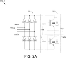
- FIG. 2A is a schematic diagram of a power cell 110-1 with a six-power semiconductor device rectifier 150 and a two-power semiconductor device inverter 155.
- the power cell 110-1 comprises a rectifier 150 and an inverter 155.
- the rectifier 150 comprises six diodes 125a.
- the rectifier 150 is connected to one secondary winding set 130ac1-3.
- the inverter 155 comprises two IGBTs 125b that output a phase of the three-phase AC output and a neutral 145N.
- Two non-power semiconductor device capacitors 195 are also shown.
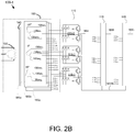
- FIG 2B is a schematic diagram of a power supply 100a of Figure 1A with power cells 110-1 of Figure 2A with a six-power semiconductor device rectifier 150 and a two-power semiconductor device inverter 155.
- each phase of the three-phases of the secondary winding sets 130 comprises three multiphase sections 185.
- the rectifier 150 of each power cell 110-1 comprises six diodes 125a.
- the inverter 155 of each power cell 110-1 comprises two IGBTs 125b. For clarity, one power cell set 115 is fully displayed and the two other power cell sets 115 are schematically displayed.
- FIG 3A is a schematic diagram of a power cell 110-2 with a six-power semiconductor device rectifier 150 and a two-power semiconductor device inverter 155.
- the power cell 110-2 comprises a rectifier 150 and an inverter 155.
- the rectifier 150 comprises six IGBTs 125b.
- the rectifier 150 is connected to one secondary winding set 130ac1-3.
- the inverter 155 comprises two IGBTs 125b that output a phase 160A-C of the three-phase AC output and a neutral 145N.
- Two non-power semiconductor device capacitors 195 are also shown.
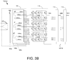
- FIG 3B is a schematic diagram of a power supply 100a of Figure 1A with power cells 110-2 of Figure 3A with a six-semiconductor power device rectifier 150 and a two-semiconductor power device inverter 155.
- Each phase of the three-phases of the secondary winding sets 130 comprises three multiphase sections 185.
- the rectifier 150 of each power cell 110-2 comprises six IGBTs 125b.
- the inverter 155 of each power cell 110-2 comprises two IGBTs 125b. For clarity, one power cell set 115 is fully displayed and the two other power cell sets 115 are schematically displayed.
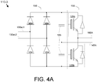
- FIG 4A is a schematic diagram of a power cell 110-3 with a four-semiconductor power device rectifier 150 and a two-semiconductor power device inverter 155.
- the power cell 110-3 comprises a rectifier 150 and an inverter 155.
- the rectifier 150 comprises four diodes 125a.
- the rectifier 150 is connected to one secondary winding set 130ac1-2.
- the inverter 155 comprises two IGBTs 125b that output a phase 160A-C of the three-phase AC output and a neutral 145N.
- Two non-power semiconductor device capacitors 195 are also shown.
- Figure 4B is a schematic diagram of a power supply 110b of Figure 1B with power cells 110-3 of Figure 4A with a four- semiconductor power device rectifier 150 and a two- semiconductor power device inverter 155.
- the phase shifting transformer 105 comprises 3 secondary winding sets 130 with 20-degree phase shifts among the voltage provided each secondary winding set 130.
- the rectifier 150 of each power cell 110-3 comprises four diodes 125a.
- the inverter 155 of each power cell 110-3 comprises two IGBTs 125b. For clarity, one power cell set 115 is fully displayed and the two other power cell sets 115 are schematically displayed.
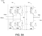
- FIG. 5A is a schematic diagram of a power cell 110-4 with a four-semiconductor power device rectifier 150 and a two-semiconductor power device inverter 155.
- the power cell 110-4 comprises a rectifier 150 and an inverter 155.
- the rectifier 150 comprises four IGBTs 125b.
- the rectifier 150 is connected to one secondary winding set 130ac1-2.
- the inverter 155 comprises two IGBTs 125b that output a phase 160A-C of the three-phase AC output and a neutral 145N.
- Two non-power semiconductor device capacitors 195 are also shown.
- FIG. 5B is a schematic diagram of a power supply 100b of Figure 1B with power cells 110-4 of Figure 5A with a four-semiconductor power device rectifier 150 and a two-semiconductor power device inverter 155.
- the rectifier 150 of each power cell 110-4 comprises four IGBTs.
- the inverter 155 of each power cell 110-4 comprises two IGBTs 125b.
- each power cell 110-4 comprises an LCL filter 15 that filters the current from the secondary winding set 130. For clarity, one power cell set 115 is fully displayed and the two other power cell sets 115 are schematically displayed.
- FIG 6A is a schematic diagram of a power cell 110-5 with a two-semiconductor power device rectifier 150 and a four-semiconductor power device inverter 155.
- the power cell 110 comprises a rectifier 150 and an inverter 155.
- the rectifier 150 comprises two diodes 125a.
- the rectifier 150 is connected to one secondary winding set 130ac1-2.
- the inverter 155 comprises four IGBTs 125b that output a phase 160A-C of the three-phase AC output and a neutral 145N.
- Two non-power semiconductor device capacitors 195 are also shown.
- Figure 6B is a schematic diagram of a power supply 100b of Figure 1B with power cells 110-5 with a two-semiconductor power device rectifier 150 and a four-semiconductor power device inverter 155.
- the rectifier 150 of each power cell 110-5 comprises two diodes 125a.
- the inverter 155 of each power cell 110-5 comprises four IGBTs 125b. For clarity, one power cell set 115 is fully displayed and the two other power cell sets 115 are schematically displayed.
- FIG. 7A is a schematic diagram of a power cell 110-6 with a two-semiconductor power device rectifier 150 and a four-semiconductor power device inverter 155.
- the power cell 110-6 comprises a rectifier 150 and an inverter 155.
- the rectifier 150 comprises two IGBTs 125b.
- the rectifier 150 is connected to one secondary winding set 130ac1-2.
- the inverter 155 comprises four IGBTs 125b that output a phase 160A-C of the three-phase AC output and a neutral 145N.
- Two non-power semiconductor device capacitors 195 are also shown.
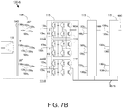
- FIG 7B is a schematic diagram of a power supply 100b of Figure 1B with power cells 110-6 of Figure 7A with a two-semiconductor power device rectifier 150 and a four-semiconductor power device inverter 155.
- the rectifier 150 of each power cell 110-6 comprises two IGBTs 125b.
- the inverter 155 of each power cell 110-6 comprises four IGBTs 125b.
- each power cell 110-6 comprises an LCL filter 15. For clarity, one power cell set 115 is fully displayed and the two other power cell sets 115 are schematically displayed.
- FIG 8A is a schematic diagram of a power cell 110-7 with a two-semiconductor power device rectifier 150 and a two-semiconductor power device inverter 155.
- the power cell 110-7 comprises a rectifier 150 and an inverter 155.
- the rectifier 150 comprises two diodes 125a.
- the rectifier 150 is connected to one secondary winding set 130ac1-2.
- the inverter 155 comprises two IGBTs 125b that output a phase 160A-C of the three-phase AC output and a neutral 145N.
- Two non-power semiconductor device capacitors 195 are also shown.
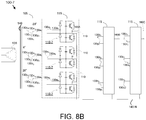
- Figure 8B is a schematic diagram of a power supply 100b of Figure 1B with power cells 110-7 of Figure 8A with a two-semiconductor power device rectifier 150 and a two-semiconductor power device inverter 155.
- the rectifier 150 of each power cell 110-7 comprises two diodes 125a.
- the inverter 155 of each power cell 110-7 comprises two IGBTs 125b.
- one power cell set 115 is fully displayed and the two other power cell sets 115 are schematically displayed.
- FIG 9A is a schematic diagram of a power cell 110-8 with a two-semiconductor power device rectifier 150 and a two-semiconductor power device inverter 155.
- the power cell 110-8 comprises a rectifier 150 and an inverter 155.
- the rectifier 150 comprises two IGBTs 125b.
- the rectifier 150 is connected to one secondary winding set 130ac1-2.
- the inverter 155 comprises two IGBTs 125b that output a phase 160A-C of the three-phase AC output and a neutral 145N.
- Two non-power semiconductor device capacitors 195 are also shown.
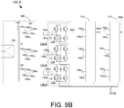
- FIG. 9B is a schematic diagram of a power supply 100b of Figure 1B with power cells 110-8 of Figure 9A with a two-semiconductor power device rectifier 150 and a two-semiconductor power device inverter 155.
- the rectifier 150 of each power cell 110-8 comprises two IGBTs 125b
- the inverter 155 of each power cell 110 comprises two IGBTs 125b.
- each power cell 110-8 comprises an LCL filter 15.
- one power cell set 115 is fully displayed and the two other power cell sets 115 are schematically displayed.
- Figure 10 is a flow chart diagram of a power supply method 500.
- the method 500 may be performed by the power supply 100.
- the method 500 may provide 501 a phase shifting transformer 105 that receives the three-phase primary voltage and steps the three-phase primary voltage down to the secondary voltage with a plurality of secondary winding sets 130a-c. In one embodiment, there is phase shifting between different secondary winding sets 130.
- the method may further provide 503 a plurality of power cell sets 115 that each comprise a plurality of power cells 110 cascaded connected.
- Each power cell 110 may receive one of a single phase and a three-phase voltage of a distinct secondary winding set 130 of the phase shifting transformer 105.
- Each power cell 110 may comprise no more than eight power semiconductor devices 125 organized as a rectifier 150 and an inverter 155.
- Each power semiconductor device 125 may be one of a diode 125a and an IGBT 125b.
- Each IGBT may comprise an anti-parallel diode 143.
- Each power cell set 115 may generate one phase of a three-phase AC output.
- Figure 11 is graphs of power supply outputs that compares the line-to-line output voltage 201, the line-to-line harmonics 203, the line-to-neutral output voltage 205, and the line-to-neutral current 207 for the output of a prior art power cell, the power cell 110-1 of Figure 2A , the power cell 110-3 of Figure 4A , the power cell 110-5 of Figure 6A , and the power cell 110-7 of Figure 8A .
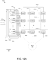
- FIG 12A is a schematic diagram of a power supply 100c.
- the power supply 100c may be a cascade H bridge power supply 100 that supports regeneration.
- the power supply 100c supplies a three-phase AC output 160 with variable voltage and frequency to a load such as the motor 123.
- the power supply 100c includes a phase shifting transformer 105 and a plurality of power cell sets 115.
- the phase shifting transformer 105 includes primary winding 135, a core 140, and a plurality of 3k secondary winding sets 130, where k is an integer.
- the primary winding 135 of the phase shifting transformer 105 receives the three-phase primary voltage.
- the plurality of secondary winding sets 130 are magnetically coupled with the primary winding 135 and step the three-phase primary voltage up or down to a secondary voltage with the plurality of first phase voltages, the plurality of second phase voltages, and the plurality of third phase voltages.
- the first, second, and third phase voltages are shown hereafter in Figures 13B-D .
- the transformer 105 employs a Wye (Y) connected primary winding 135 and zigzag connected secondary winding sets 130.
- the transformer 105 may also employ a Delta ( ⁇ ) connected primary winding 135, an extended-Delta ( ⁇ ) secondary winding set 130, and/or polygon connected secondary winding sets 130.
- the plurality of three power cell sets 115 each comprise a plurality of power cells 110 cascaded connected. Each power cell set 115 comprises k power cells 110. Each power cell set 115 generates one phase of a three-phase AC output 160A-C.
- the phase shifting transformer 105 comprises 3k secondary winding sets 130 and three power cell rows 113-1-k.
- the power cells 110 may be controlled by the controller 127 with sinusoidal pulse width modulation control signals.
- the power cells 110 are controlled with modulation control signals selected from the group consisting of sinusoidal pulse width modulation control signals, modified pulse width modulation control signals, random pulse width modulation control signals, third harmonic injection pulse width modulation control signals, and space vector modulation control signals.
- the carrier phase shifting angles of the rectifiers 150 in the power cell sets 115 may be shifted by 120 degrees from each other.
- the switching frequency for the modulation control signals is 1980 Hz.
- FIG 12B is a schematic diagram of a power supply 100d.
- the power supply 100d may be a cascade H bridge power supply 100 that supports regeneration.
- the power supply 100d supplies a three-phase AC output 160 with variable voltage and frequency to a load.
- the load is a motor 123.
- the AC output 160 may drive one or more motors 123 as the load.
- the power supply 100d includes a phase shifting transformer 105 and a plurality of power cell sets 115.
- the phase shifting transformer 105 includes primary winding 135, a core 140, and a plurality of secondary winding sets 130.
- the primary winding 135 of the phase shifting transformer 105 receives the three-phase primary voltage.
- the plurality of secondary winding sets 130 are magnetically coupled with the primary winding 135 and step the three-phase primary voltage up or down to a secondary voltage with a plurality of first phase voltages, a plurality of second phase voltages, and a plurality of third phase voltages.
- the transformer 105 employs a Wye (Y) connected primary winding 135 and zigzag connected secondary winding sets 130.
- the transformer 105 may also employ a Delta ( ⁇ ) connected primary winding 135, an extended-Delta ( ⁇ ) secondary winding set 130, and/or polygon connected secondary winding sets 130.
- the plurality of power cell sets 115 each comprise a plurality of power cells 110 cascaded connected. Each power cell set 115 generates one phase of a three-phase AC output 160A-C.
- the phase shifting transformer 105 comprises 9 secondary winding sets 130 and three power cell rows 113-1-3. In one embodiment, there is secondary phase shifting between the different secondary winding sets 130.
- the power cells 110 may be controlled by a controller 127 with sinusoidal pulse width modulation control signals.
- the power cells 110 are controlled with modulation control signals selected from the group consisting of sinusoidal pulse width modulation control signals, modified pulse width modulation control signals, random pulse width modulation control signals, third harmonic injection pulse width modulation control signals, and space vector modulation control signals.
- the carrier angles ⁇ 1 , ⁇ 2 , and ⁇ 3 for rectifier 150 in the power cells 110-1, 110-2, and 110-3 may be phase shifted by 120 degrees.
- the switching frequency for the modulation control signals is 1980 Hz.
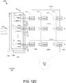
- FIG 12C is a schematic diagram of a power supply 100e.
- the power supply 100e may be a cascade H bridge power supply 100 that supports regeneration.
- the power supply 100e supplies a three-phase AC output 160 with variable voltage and frequency to a load such as the motor 123.
- the power supply 100e includes a phase shifting transformer 105 and a plurality of power cell sets 115.
- the phase shifting transformer 105 includes primary winding 135, a core 140, and a plurality of 3k secondary winding sets 130, where k is an integer.
- the primary winding 135 of the phase shifting transformer 105 receives the three-phase primary voltage.
- the plurality of secondary winding sets 130 are magnetically coupled with the primary winding 135 and step the three-phase primary voltage up or down to a secondary voltage with the plurality of first phase voltages, the plurality of second phase voltages, and the plurality of third phase voltages.
- the transformer 105 employs a Wye (Y) connected primary winding 135 and zigzag connected secondary winding sets 130.
- the transformer 105 may also employ a Delta ( ⁇ ) connected primary winding 135 and/or and extended-Delta ( ⁇ ) secondary winding set 130, and/or polygon connected secondary winding sets 130.
- the plurality of three power cell sets 115 each comprise a plurality of power cells 110 cascaded connected. Each power cell set 115 comprises k power cells 110. Each power cell set 115 generates one phase of a three-phase AC output 160A-C.
- the power cells 110 may be controlled by the controller 127 with sinusoidal pulse width modulation control signals.
- the power cells 110 are controlled with modulation control signals selected from the group consisting of sinusoidal pulse width modulation control signals, modified pulse width modulation control signals, random pulse width modulation control signals, third harmonic injection pulse width modulation control signals, and space vector modulation control signals.
- the carrier angles ⁇ for the rectifiers 150 in each power cell row 113-n may be the same.
- the carrier angles a first row 113-1 may be ⁇ 1 degrees.
- the carrier phase shifting angles ⁇ 1 , ⁇ 2 , ..., ⁇ k of rectifiers 150 in different power cell rows 113 may be shifted by 360 k degrees from each other.
- the switching frequency for the modulation control signals is 1980 Hz.
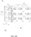
- FIG 12D is a schematic diagram of a power supply 100f.
- the power supply 100f may be a cascade H bridge power supply 100 that supports regeneration.
- the power supply 100f supplies a three-phase AC output 160 with variable voltage and frequency to a load such as the motor 123.
- the power supply 100f includes a phase shifting transformer 105 and a plurality of power cell sets 115.
- the phase shifting transformer 105 includes primary winding 135, a core 140, and a plurality of secondary winding sets 130.
- the primary winding 135 of the phase shifting transformer 105 receives the three-phase primary voltage.
- the plurality of secondary winding sets 130 are magnetically coupled with the primary winding 135 and step the three-phase primary voltage up or down to a secondary voltage with the plurality of first phase voltages, the plurality of second phase voltages, and the plurality of third phase voltages.
- the transformer 105 employs a Wye (Y) connected primary winding 135 and zigzag connected secondary winding sets 130.
- the transformer 105 may also employ a Delta ( ⁇ ) connected primary winding 135, an extended-Delta ( ⁇ ) secondary winding set 130, and/or polygon connected secondary winding sets 130.
- the plurality of power cell sets 115 each comprise a plurality of power cells 110 cascaded connected. Each power cell set 115 generates one phase of a three-phase AC output 160A-C.
- the power cells 110 may be controlled by the controller 127 with sinusoidal pulse width modulation control signals.
- the power cells 110 are controlled with modulation control signals selected from the group consisting of sinusoidal pulse width modulation control signals, modified pulse width modulation control signals, random pulse width modulation control signals, third harmonic injection pulse width modulation control signals, and space vector modulation control signals.
- Figure 13A is a schematic diagram of an active switch 125b.
- the active switch 125b includes an anti-parallel diode 143.
- the active switch 125b is controlled by a modulation control signal 129 from the controller 127.
- FIGS 13B-D are schematic diagram of a power cell 110.
- Each power cell 110 comprises a rectifier 150 and an inverter 155.
- the inverter 155 is an H-bridge of four active switches 125b.
- the inverter 155 outputs a phase of the AC output 160 and connects to the neutral 145.
- the rectifier 150 comprising two first active switches 125b-1 that are serially connected and receive a phase voltage 131 at a first switch midpoint 133-1, two second active switches 125b-2 that are serially connected and receive another phase voltage 131 at a second switch midpoint 133-2, and two capacitors 195 that are serially connected and receive another phase voltage 131 at a capacitor midpoint 133-3 between the capacitors 195, wherein the two first active switches 125b-1, the second two first active switches 125b-2, and the two capacitors 195 of each power cell 110 are connected in parallel.
- the distribution of phase voltages 131 at the first switch midpoint 133-1, the second switch midpoint 133-2, and the capacitor midpoint 133-3 reduces harmonics of a primary current harmonic spectrum as is shown hereafter.
- a first power cell 110-1 is shown.
- a second phase voltage 131-2 is connected to the first switch midpoint 133-1, a third phase voltage 131-3 is connected to the second switch midpoint 133-2, and a first phase voltage 131-1 is connected to the capacitor midpoint 133-3.
- the third phase voltage 131-3 is connected to the first switch midpoint 133-1, the first phase voltage 131-1 is connected to the second switch midpoint 133-2, and the second phase voltage 131-2 is connected to the capacitor midpoint 133-3 for a second power cell 110-2.
- the first phase voltage 131-1 is connected to the first switch midpoint 133-1
- the second phase voltage 131-2 is connected to the second switch midpoint 133-2
- the third phase voltage 131-3 is connected to the capacitor midpoint 133-3 for a third power cell 110-3.
- the connections are employed for the power supplies 100e/100f of Figures 12C-D and for some embodiments for the power supplies 100c/100d of Figures 12 A-B .
- the power cells 110 in the power supplies 100c/100d of Figure 12 A and 12B may be connected to the secondary winding sets as follows: For the first power cells 110-1, the first switch midpoint 133-1 receives the second phase voltage 131-2 from an av secondary winding set 130-av, the second switch midpoint 133-2 receives the third phase voltage 131-3 from an aw secondary winding set 130-aw, and the capacitor midpoint 133-3 receives the first phase voltage 131-1 from an au secondary winding set 130-au.
- the first switch midpoint 133-1 receives the third phase voltage 131-3 from a bw secondary winding set 130-bw
- the second switch midpoint 133-2 receives the first phase voltage 131-1 from a bu secondary winding set 130-bu
- the capacitor midpoint 133-3 receives the second phase voltage 131-2 from a bv secondary winding set 130-bv.
- the first switch midpoint 133-1 receives the first phase voltage 131-1 from a cu secondary winding set 130-cu
- the second switch midpoint 133-2 receives the second phase voltage 131-2 from a cv secondary winding set 130-cv
- the capacitor midpoint 133-3 receives the third phase voltage 131-3 from a cw secondary winding set 130-cw.
- the embodiments include electrical equivalents.
- the first switch midpoint 133-1, the second switch midpoint 133-2, and the third switch midpoint 133-3 are connected in a same phase sequence.
- the embodiments include electrical equivalents.
- the power cells 110 in the power supplies 100c/100d of Figure 12A and 12B are connected to the secondary winding sets as follows:
- the first switch midpoint 133-1 receives the same phase voltage 131-1 from a u secondary winding set 130-un
- the second switch midpoint 133-2 receives the second phase voltage 131-2 from a v secondary winding set 130-vn
- the capacitor midpoint 133-3 receives the third phase voltage 131-3 from a w secondary winding set 130-wn.
- the first switch midpoint 133-1 receives the third phase voltage 131-3 from a bw secondary winding set 130-bw
- the second switch midpoint 133-2 receives the first phase voltage 131-1 from a bu secondary winding set 130-bu
- the capacitor midpoint 133-3 receives the second phase voltage 131-2 from a bv secondary winding set 130-bv, and for a power cell row 113-z.
- the first switch midpoint 133-1 receives the first phase voltage 131-1 from a cu secondary winding set 130-cu
- the second switch midpoint 133-2 receives the second phase voltage 131-2 from a cv secondary winding set 130-cv
- the capacitor midpoint 133-3 receives the third phase voltage 131-3 from a cw secondary winding set 130-cw.
- the embodiments include electrical equivalents.
- the first switch midpoint 133-1 receives the second phase voltage 131-2 from an av secondary winding set 130-av
- the second switch midpoint 133-2 receives the third phase voltage 131-3 from an aw secondary winding set 130-aw
- the capacitor midpoint 133-3 receives the first phase voltage 131-1 from an au secondary winding set 130-au
- the first switch midpoint 133-1 receives the third phase voltage 131-3 from a bw secondary winding set 130-bw
- the second switch midpoint 133-2 receives the first phase voltage 131-1 from a bu secondary winding set 130-bu
- the capacitor midpoint 133-3 receives the second phase voltage 131-2 from a bv secondary winding set 130-bv
- the first switch midpoint 133-1 receives the first phase voltage 131-1 from a
- Table 3 Secondary Winding Output 130 Power Cell 110 Phase Voltage 131 130-av 113-1 133-1 130-aw 113-1 133-2 130-au 113-1 133-3 130-bw 113-2 133-1 130-bu 113-2 133-2 130-bv 113-2 133-3 130-cu 113-3 133-1 130-cv 113-3 133-2 130-cw 113-3 133-3
- the power cells 110 in the power supply 100e/100fof Figure 12C and 12D may be connected to the secondary winding sets as follows.
- the first switch midpoint 133-1 receives the second phase voltage 131-2 from an av secondary winding set 130-av
- the second switch midpoint 133-2 receives the third phase voltage 131-3 from an aw secondary winding set 130-aw
- the capacitor midpoint 133-3 receives the first phase voltage 131-1 from an au secondary winding set 130-au.
- the first switch midpoint 133-1 receives the third phase voltage 131-3 from a bw secondary winding set 130-bw
- the second switch midpoint 133-2 receives the first phase voltage 131-1 from a bu secondary winding set 130-bu
- the capacitor midpoint 133-3 receives the second phase voltage 131-2 from a bv secondary winding set 130-bv.
- the first switch midpoint 133-1 receives the first phase voltage 131-1 from a cu secondary winding set 130-cu
- the second switch midpoint 133-2 receives the second phase voltage 131-2 from a cv secondary winding set 130-cv
- the capacitor midpoint 133-3 receives the third phase voltage 131-3 from a cw secondary winding set 130-cw.
- Table 4 Secondary Winding Output 130 Power Cell 110 Phase Voltage 131 130-av 110-1 133-1 130-aw 110-1 133-2 130-au 110-1 133-3 130-bw 110-2 133-1 130-bu 110-2 133-2 130-bv 110-2 133-3 130-cu 110-3 133-1 130-cv 110-3 133-2 130-cw 110-3 133-3
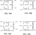
- Figures 14A-D are schematic diagrams of power cell switching.
- the controller 127 controls the modulation control signals 129 so that the active switches 125 are switched.
- Figure 14A shows a first position with active switch 125-11 and active switch 125-22 on and active switch 125-12 and active switch 125-21 off.
- Figure 14B shows a second position with active switch 125-11 and active switch 125-21 on and active switch 125-12 and active switch 125-22 off.
- Figure 14C shows a third position with active switch 125-12 and active switch 125-21 on and active switch 125-11 and active switch 125-22 off.
- Figure 14D shows a fourth position with active switch 125-12 and active switch 125-22 on and active switch 125-11 and active switch 125-21 off.
- Figure 15 is a graph of power cell phase voltages 121 for the power cell switching of Figures 14A-D .
- the switching results in two opposite direct/quadrature vectors 121 that are equal in magnitude and 180 degrees out of phase.
- Phase voltage 121-1 is for the power cell switching of Figure 14A
- phase voltage 121-2 is for the power cell switching of Figure 14B
- phase voltage 121-3 is for the power cell switching of Figure 14C
- phase voltage 121-4 is for the power cell switching of Figure 14D .
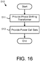
- Figure 16 is a flow chart diagram of a power supply method 510.
- the method 510 provides power to a load such as the motor 123 and may be performed by the power supply 100.
- the method 410 may provide 511 a transformer 105 that receives a three-phase primary voltage and steps the three-phase primary voltage up or down to a secondary voltage with a plurality of secondary winding sets 130 to a plurality of first phase voltages 131-1, a plurality of second phase voltages 131-2, and a plurality of third phase voltages 131-3.
- the method 510 further provides 513 a plurality of power cell sets 115 that each comprise a plurality of power cells 110 cascaded connected.
- Each power cell 110 comprises a rectifier 150 and an inverter 155.
- the rectifier 150 comprises two first active switches 125b-1 that are serially connected and receive a phase voltage 131 at a first switch midpoint 133-1, two second active switches 125b-2 that are serially connected and receive another phase voltage 131 at a second switch midpoint 133-2, and two capacitors 195 that are serially connected and receive another phase voltage 131 at a capacitor midpoint 133-3 between the capacitors 195.
- the two first active switches 125b-1, the second two first active switches 125b-2, and the two capacitors 195 of each power cell 110 are connected in parallel.
- Figure 17A is a graph of power supply harmonic spectrums for the power supply 100 of Figure 12B .
- the switching frequency is 4020 Hz with the connections of Table 1.
- the carrier angles are the same for the rectifiers 150 in all power cells 110.
- the secondary currents harmonic spectrum for the secondary winding sets 130 and the primary currents harmonic spectrum for the primary winding 135 are shown as magnitudes 601 expressed as a percentage to the fundamental harmonic.
- the total harmonic distortion (THD) is also specified.
- Figure 17B is graphs of power supply output currents la, Ib, and Ic for the AC outputs 160 of the power supply 100 of Figure 12B .
- the currents 603 are measured per unit.
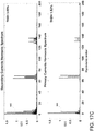
- Figure 17C is graphs of power supply harmonic spectrums for the power supply 100 of Figure 12B .
- the switching frequency is 4020 Hz with the connections of Table 2.
- the carrier angles are the same for the rectifiers 150 in all power cells 110.
- the secondary currents harmonic spectrum for the secondary winding sets 130 and the primary currents harmonic spectrum for the primary winding 135 are shown as magnitudes 601 expressed as a percentage to the fundamental harmonic.
- the THD is also specified.
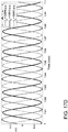
- Figure 17D is a graph of power supply output currents la, Ib, and Ic for the AC outputs 160 of the power supply 100 of Figure 12B .
- the currents 603 are measured per unit.
- Figure 17E are graphs of a motor speed profile and motor torque for the motor 123 of Figure 12B .
- the speed 607 measured in per unit and torque 609 measured in per unit are shown while motoring and during regeneration over a time interval
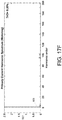
- Figure 17F is a graph of a power supply harmonic spectrum for the power supply 100 of Figure 12D during motoring.
- the switching frequency is 1980 Hz
- the connection of table 4 is used, and the carrier angles for the rectifiers 150 in the power cell rows 113-1/2/3 are shifted by 120 degrees.
- the primary current harmonic spectrum for the primary winding 135 is shown as magnitudes 601 expressed as a percentage to the fundamental harmonic.
- the THD is also specified.
- Figure 17G is a graph of a power supply harmonic spectrum for the power supply 100 of Figure 12D during regeneration.
- the switching frequency is 1980 Hz
- the connection of table 4 is used, and the carrier angles for the rectifiers 150 in the power cell rows 113-1/2/3 are shifted by 120 degrees.
- the primary current harmonic spectrum for the primary winding 135 is shown as magnitudes 601 expressed as a percentage to the fundamental harmonic.
- the THD is also specified.
- Figure 17H is a graph of a power supply harmonic spectrum for the power supply 100 of Figure 12B during motoring.
- the switching frequency is 1980 Hz
- the connections of Table 3 are used, and the carrier angles for the rectifiers 150 in the power cells 110-1/2/3 are shifted by 120 degrees.
- the primary current harmonic spectrum for the primary winding 135 is shown as magnitudes 601 expressed as a percentage to the fundamental harmonic.
- the THD is also specified.
- Figure 17I is a graph of a power supply harmonic spectrum for the power supply 100 of Figure 12B during regeneration.
- the switching frequency is 1980 Hz
- the connections of Table 3 are used, and the carrier angles for the rectifiers 150 in the power cells 110-1/2/3 are shifted by 120 degrees.
- the primary current harmonic spectrum for the primary winding 135 is shown as magnitudes 601 expressed as a percentage to the fundamental harmonic.
- the THD is also specified.
- a cascaded H bridge power supply 100 may typically have at least six active switches 125b in the rectifier 150. Reducing the power semiconductor devices 125 significantly reduces the cost of the power supply 100.
- the embodiments employ power cells 110 with reduced active switches 125b in the rectifier 150. As a result, the embodiments enable regenerative power supplies 100 with significantly reduced cost.
Landscapes
- Engineering & Computer Science (AREA)
- Power Engineering (AREA)
- Inverter Devices (AREA)
Abstract
Description
- This is a continuation-in-part application of and claims priority to United States Patent Application Number
16/393,613 - subject matter disclosed herein relates to power supplies and more particularly to regenerative cascaded H bridge power supplies.
- A power supply based on cascaded power cells with a reduced number of semiconductor devices is disclosed. The power supply includes a transformer and a plurality of power cell sets. The transformer receives a three-phase primary voltage and steps the three-phase primary voltage up or down to a secondary voltage with a plurality of secondary winding sets to a plurality of first phase voltages, a plurality of second phase voltages, and a plurality of third phase voltages. The plurality of power cell sets each comprise a plurality of power cells cascaded connected. Each power cell comprises a rectifier and an inverter. The rectifier comprises two first active switches that are serially connected and receive a phase voltage at a first switch midpoint, two second active switches that are serially connected and receive another phase voltage at a second switch midpoint, and two capacitors that are serially connected and receive another phase voltage at a capacitor midpoint between the capacitors. The two first active switches, the second two first active switches, and the two capacitors of each power cell are connected in parallel. An apparatus and a drive also perform the functions of the power supply.
- In order that the advantages of the embodiments of the invention will be readily understood, a more particular description of the embodiments briefly described above will be rendered by reference to specific embodiments that are illustrated in the appended drawings. Understanding that these drawings depict only some embodiments and are not therefore to be considered to be limiting of scope, the embodiments will be described and explained with additional specificity and detail through the use of the accompanying drawings, in which:
-
Figure 1A is a schematic diagram of a power supply according to an embodiment; -
Figure 1B is a schematic diagram of a power supply according to an alternate embodiment; -
Figure 1C is a schematic diagram of power semiconductor devices according to an embodiment. -
Figure 2A is a schematic diagram of a power cell with a six-device rectifier and a two-device inverter according to an embodiment; -
Figure 2B is a schematic diagram of a power supply with power cells with a six-device rectifier and a two-device inverter according to an embodiment; -
Figure 3A is a schematic diagram of a power cell with a six-device rectifier and a two-device inverter according to an alternate embodiment; -
Figure 3B is a schematic diagram of a power supply with power cells with a six-device rectifier and a two-device inverter according to an alternate embodiment; -
Figure 4A is a schematic diagram of a power cell with a four-device rectifier and a two-device inverter according to an embodiment; -
Figure 4B is a schematic diagram of a power supply with power cells with a four-device rectifier and a two-device inverter according to an embodiment; -
Figure 5A is a schematic diagram of a power cell with a four-device rectifier and a two-device inverter according to an alternate embodiment; -
Figure 5B is a schematic diagram of a power supply with power cells with a four-device rectifier and a two-device inverter according to an alternate embodiment; -
Figure 6A is a schematic diagram of a power cell with a two-device rectifier and a four-device inverter according to an embodiment; -
Figure 6B is a schematic diagram of a power supply with power cells with a two-device rectifier and a four-device inverter according to an embodiment; -
Figure 7A is a schematic diagram of a power cell with a two-device rectifier and a four-device inverter according to an alternate embodiment; -
Figure 7B is a schematic diagram of a power supply with power cells with a two-device rectifier and a four-device inverter according to an alternate embodiment; -
Figure 8A is a schematic diagram of a power cell with a two-device rectifier and a two-device inverter according to an embodiment; -
Figure 8B is a schematic diagram of a power supply with power cells with a two-device rectifier and a two-device inverter according to an embodiment; -
Figure 9A is a schematic diagram of a power cell with a two-device rectifier and a two-device inverter according to an alternate embodiment; -
Figure 9B is a schematic diagram of a power supply with power cells with a two-device rectifier and a two-device inverter according to an alternate embodiment; -
Figure 10 is a flow chart diagram of a power supply method according to an embodiment; -
Figure 11 is graphs of power supply outputs according to an embodiment; -
Figure 12A is a schematic diagram of a power supply according to an embodiment; -
Figure 12B is a schematic diagram of an alternate power supply according to an embodiment; -
Figure 12C is a schematic diagram of an alternate power supply according to an embodiment; -
Figure 12D is a schematic diagram of an alternate power supply according to an embodiment; -
Figure 13A is a schematic diagram of an active switch according to an embodiment; -
Figures 13B-D are schematic diagram of a power cell according to an embodiment; -
Figures 14A-D are schematic diagrams of power cell switching according to an embodiment; -
Figure 15 is a graph of power cell phase voltages according to an embodiment; -
Figure 16 is a flow chart diagram of a power supply method according to an alternate embodiment; -
Figure 17A is graphs of power supply harmonic spectrums according to an embodiment; -
Figure 17B is a graph of power supply output currents according to an embodiment; -
Figure 17C is graphs of power supply harmonic spectrums according to an alternate embodiment; -
Figure 17D is a graph of power supply output currents according to an alternate embodiment; -
Figure 17E are graphs of a motor speed profile and motor torque according to an embodiment; -
Figure 17F is a graph of a power supply harmonic spectrum according to an embodiment; -
Figure 17G is a graph of a power supply harmonic spectrum according to an embodiment; -
Figure 17H is a graph of a power supply harmonic spectrum according to an alternate embodiment; and -
Figure 17I is a graph of a power supply harmonic spectrum according to an alternate embodiment. - Reference throughout this specification to "one embodiment," "an embodiment," or similar language means that a particular feature, structure, or characteristic described in connection with the embodiment is included in at least one embodiment. Thus, appearances of the phrases "in one embodiment," "in an embodiment," and similar language throughout this specification may, but do not necessarily, all refer to the same embodiment, but mean "one or more but not all embodiments" unless expressly specified otherwise. The terms "including," "comprising," "having," and variations thereof mean "including but not limited to" unless expressly specified otherwise. An enumerated listing of items does not imply that any or all of the items are mutually exclusive and/or mutually inclusive, unless expressly specified otherwise. The terms "a," "an," and "the" also refer to "one or more" unless expressly specified otherwise.
- The schematic flowchart diagrams and/or schematic block diagrams in the Figures illustrate the architecture, functionality, and operation of possible implementations. It should also be noted that, in some alternative implementations, the functions noted in the block may occur out of the order noted in the Figures. For example, two blocks shown in succession may, in fact, be executed substantially concurrently, or the blocks may sometimes be executed in the reverse order, depending upon the functionality involved. Although various arrow types and line types may be employed in the flowchart and/or block diagrams, they are understood not to limit the scope of the corresponding embodiments. Indeed, some arrows or other connectors may be used to indicate only an exemplary logical flow of the depicted embodiment.
- The description of elements in each figure may refer to elements of proceeding figures. Like numbers refer to like elements in all figures, including alternate embodiments of like elements.
-
Figure 1A is a schematic diagram of apower supply 100a. Thepower supply 100a supplies a three-phase AC output with variable voltage and frequency to the load. The AC output may drive one or more motors as the load. Thepower supply 100a includes aphase shifting transformer 105 and a plurality of power cell sets 115. - In the depicted embodiment, the
phase shifting transformer 105 includes primary winding 135, acore 140, and a plurality of secondary winding sets 130. The primary winding 135 of thephase shifting transformer 105 receives the three-phase primary voltage. The plurality of secondary windingsets 130 are magnetically coupled with the primary winding 135 and step the three-phase primary voltage up or down to a secondary voltage. In one embodiment, there is phase shifting between the different secondary winding sets 130. Thetransformer 105 is shown with Delta (Δ) connected primary winding 135 and zigzag connected secondary winding sets 130. It can also be Wye (Y) connected primary winding 135 and extended-Delta (Δ) secondary winding set 130, or polygon connected secondary windingset 130. - In the depicted embodiment, the
phase shifting transformer 105 comprises 9 secondary windingsets 130 with 20 degree phase shifts among the voltage provided by the top three secondary windingsets 130a, the middle three secondary winding sets 130b, and the bottom three secondary winding sets 130c as indicated inFigure 1A . each secondary winding set 130 provide the secondary voltage with the specified phase to the power cell sets 115. - In this embodiment, an exemplary 9 power cells circuit is shown. The number of
power cells 110 may change depending on the requirement of the output voltage, thus the number of secondary windingsets 130 for each power cell set 115 will change accordingly. Generally speaking, the same circuit topology can be used for any number n ofpower cells 110 in series in each power cell set 115, and there will be the same amount of secondary windingsets 130 feeding each of thepower cells 110. The phase shifting angles shown inFig. 1A is also exemplary for n=3. These angles can be changed. In general, for n secondary windingsets 130 feedingn power cells 110 of each three-phase power cell set 115A-C, the phase shift angle within each set is 60°/n, or 20°/n. For example, if n = 4, the phase shift angle of the transformersecondary windings 130 for each power cell set 115 is 60°/4=15°, or 20°/4=5°. If n=5, the phase shift angle will be 60°/5=12°, or 20°/5=4°, and so on. - The plurality of power cell sets 115 each comprise a plurality of
power cells 110 that are cascaded connected. Eachpower cell 110 receives one of a single phase and a three-phase voltage of a distinct secondary winding set 130 of thephase shifting transformer 105. Each power cell set 115 generates onephase 160A-C of a three-phase AC output. - The
power cells 110 include a plurality of semiconductor devices to rectify and invert the voltage received from a secondary winding set 130 into aphase 160A-C of the three-phase AC output. As more semiconductor devices are used in thepower cells 110, the cost and size of thepower cells 110 and thepower supply 100a are increased. The embodiments reduce the number of semiconductor devices in thepower cells 110 and/orpower supply 100 to reduce the cost and size of thepower supply 100. In one embodiment, eachpower cell 110 comprises no more than eight power semiconductor devices. Thepower supply 100 is organized to provide the AC output with the reduced number of power semiconductor devices, resulting in significant cost savings. -
Figure 1B is an exemplary schematic diagram of apower supply 100b. In the depicted embodiment, thephase shifting transformer 105 comprises 3 secondary windingsets 130 with 20-degree phase shifts among the voltage provided each secondary windingset 130. It differs fromFigure 1A in that the three phase secondary winding sets are terminated in such way that single phase power can be provided to the power cells, thus the number of three-phase secondary windings is 1/3 comparing toFigure 1A . - In this embodiment, an exemplary 9 power cells circuit is shown. The number of power cells may change depending on the requirement of the output voltage, thus the number of
secondary windings 130 for each power cell set 115 will change accordingly. Generally speaking, the same circuit topology can be used for any number n ofpower cells 110 in series in each power cell set 115, and there will be the same amount ofsecondary windings 130 feeding each of thepower cells 110. The phase shifting angles shown inFig.1A is also exemplary for n=3. These angles may be changed. In general, for nsecondary windings 130 feedingn power cells 110 of each three-phase power cell set 115A-C, the phase shift angle within each power cell set 115 is 60°/n. For example, if n = 4, the phase shift angle of the transformersecondary windings 130 for each power cell set 115 is 60°/4=15°. If n=5, the phase shift angle will be 60°/5=12°, and so on. - The topologies shown in
Figure 1A andFigure 1B will be applied to the power cells depicted later. Exemplary n = 3 power cells per set are used to demonstrate the circuit topology. In real implementation n can be any natural number. -
Figure 1C is a schematic diagram ofpower semiconductor devices 125. As used herein, apower semiconductor device 125 is one of adiode 125a and anactive switch 125b. Thediode 125a may also be a thyristor, or other active semiconductor switches. Theactive switch 125b may be an Insulated Gate Bipolar Transistor (IGBT) 125b. In one embodiment, theactive switch 125b is field effect transistor (FET) 125b. Theactive switch 125b may be a metal-oxide semiconductor field-effect transistor (MOSFET) 125b or integrated gate commuted thyristor (IGCT). Theactive switch 125b may be other semiconductor switching devices such as silicon controlled rectifiers (SCR). The quantity of semiconductor switches is counted from circuit principle point of view. Semiconductor devices connected in parallel or series are count as single functional device. Eachactive switch 125b may comprise ananti-parallel diode 143. Apower cell 110 may have no more than eightpower semiconductor devices 125. In one embodiment, the no more than eightpower semiconductor devices 125 are organized as arectifier 150 and aninverter 155 within thepower cell 110. Therectifier 150 may selectively modify the direction of an input current. Theinverter 155 may form the required AC output. In one embodiment, apower cell 110 includes additional non-power semiconductor devices such as capacitors, connectors, connections, and the like. The numbers of non-power semiconductor devices may not be reduced. -
Figure 2A is a schematic diagram of a power cell 110-1 with a six-powersemiconductor device rectifier 150 and a two-powersemiconductor device inverter 155. In the depicted embodiment, the power cell 110-1 comprises arectifier 150 and aninverter 155. Therectifier 150 comprises sixdiodes 125a. Therectifier 150 is connected to one secondary winding set 130ac1-3. Theinverter 155 comprises twoIGBTs 125b that output a phase of the three-phase AC output and a neutral 145N. Two non-powersemiconductor device capacitors 195 are also shown. -
Figure 2B is a schematic diagram of apower supply 100a ofFigure 1A with power cells 110-1 ofFigure 2A with a six-powersemiconductor device rectifier 150 and a two-powersemiconductor device inverter 155. In the depicted embodiment, each phase of the three-phases of the secondary windingsets 130 comprises three multiphase sections 185. Therectifier 150 of each power cell 110-1 comprises sixdiodes 125a. Theinverter 155 of each power cell 110-1 comprises twoIGBTs 125b. For clarity, one power cell set 115 is fully displayed and the two other power cell sets 115 are schematically displayed. -
Figure 3A is a schematic diagram of a power cell 110-2 with a six-powersemiconductor device rectifier 150 and a two-powersemiconductor device inverter 155. In the depicted embodiment, the power cell 110-2 comprises arectifier 150 and aninverter 155. Therectifier 150 comprises six IGBTs 125b. Therectifier 150 is connected to one secondary winding set 130ac1-3. Theinverter 155 comprises twoIGBTs 125b that output aphase 160A-C of the three-phase AC output and a neutral 145N. Two non-powersemiconductor device capacitors 195 are also shown. -
Figure 3B is a schematic diagram of apower supply 100a ofFigure 1A with power cells 110-2 ofFigure 3A with a six-semiconductorpower device rectifier 150 and a two-semiconductorpower device inverter 155. Each phase of the three-phases of the secondary windingsets 130 comprises three multiphase sections 185. Therectifier 150 of each power cell 110-2 comprises six IGBTs 125b. Theinverter 155 of each power cell 110-2 comprises twoIGBTs 125b. For clarity, one power cell set 115 is fully displayed and the two other power cell sets 115 are schematically displayed. -
Figure 4A is a schematic diagram of a power cell 110-3 with a four-semiconductorpower device rectifier 150 and a two-semiconductorpower device inverter 155. In the depicted embodiment, the power cell 110-3 comprises arectifier 150 and aninverter 155. Therectifier 150 comprises fourdiodes 125a. Therectifier 150 is connected to one secondary winding set 130ac1-2. Theinverter 155 comprises twoIGBTs 125b that output aphase 160A-C of the three-phase AC output and a neutral 145N. Two non-powersemiconductor device capacitors 195 are also shown. -
Figure 4B is a schematic diagram of a power supply 110b ofFigure 1B with power cells 110-3 ofFigure 4A with a four- semiconductorpower device rectifier 150 and a two- semiconductorpower device inverter 155. Thephase shifting transformer 105 comprises 3 secondary windingsets 130 with 20-degree phase shifts among the voltage provided each secondary windingset 130. Therectifier 150 of each power cell 110-3 comprises fourdiodes 125a. Theinverter 155 of each power cell 110-3 comprises twoIGBTs 125b. For clarity, one power cell set 115 is fully displayed and the two other power cell sets 115 are schematically displayed. -
Figure 5A is a schematic diagram of a power cell 110-4 with a four-semiconductorpower device rectifier 150 and a two-semiconductorpower device inverter 155. In the depicted embodiment, the power cell 110-4 comprises arectifier 150 and aninverter 155. Therectifier 150 comprises fourIGBTs 125b. Therectifier 150 is connected to one secondary winding set 130ac1-2. Theinverter 155 comprises twoIGBTs 125b that output aphase 160A-C of the three-phase AC output and a neutral 145N. Two non-powersemiconductor device capacitors 195 are also shown. -
Figure 5B is a schematic diagram of apower supply 100b ofFigure 1B with power cells 110-4 ofFigure 5A with a four-semiconductorpower device rectifier 150 and a two-semiconductorpower device inverter 155. In the depicted embodiment, therectifier 150 of each power cell 110-4 comprises four IGBTs. Theinverter 155 of each power cell 110-4 comprises twoIGBTs 125b. In addition, each power cell 110-4 comprises anLCL filter 15 that filters the current from the secondary windingset 130. For clarity, one power cell set 115 is fully displayed and the two other power cell sets 115 are schematically displayed. -
Figure 6A is a schematic diagram of a power cell 110-5 with a two-semiconductorpower device rectifier 150 and a four-semiconductorpower device inverter 155. In the depicted embodiment, thepower cell 110 comprises arectifier 150 and aninverter 155. Therectifier 150 comprises twodiodes 125a. Therectifier 150 is connected to one secondary winding set 130ac1-2. Theinverter 155 comprises four IGBTs 125b that output aphase 160A-C of the three-phase AC output and a neutral 145N. Two non-powersemiconductor device capacitors 195 are also shown. -
Figure 6B is a schematic diagram of apower supply 100b ofFigure 1B with power cells 110-5 with a two-semiconductorpower device rectifier 150 and a four-semiconductorpower device inverter 155. Therectifier 150 of each power cell 110-5 comprises twodiodes 125a. Theinverter 155 of each power cell 110-5 comprises fourIGBTs 125b. For clarity, one power cell set 115 is fully displayed and the two other power cell sets 115 are schematically displayed. -
Figure 7A is a schematic diagram of a power cell 110-6 with a two-semiconductorpower device rectifier 150 and a four-semiconductorpower device inverter 155. In the depicted embodiment, the power cell 110-6 comprises arectifier 150 and aninverter 155. Therectifier 150 comprises twoIGBTs 125b. Therectifier 150 is connected to one secondary winding set 130ac1-2. Theinverter 155 comprises four IGBTs 125b that output aphase 160A-C of the three-phase AC output and a neutral 145N. Two non-powersemiconductor device capacitors 195 are also shown. -
Figure 7B is a schematic diagram of apower supply 100b ofFigure 1B with power cells 110-6 ofFigure 7A with a two-semiconductorpower device rectifier 150 and a four-semiconductorpower device inverter 155. In the depicted embodiment, therectifier 150 of each power cell 110-6 comprises twoIGBTs 125b. Theinverter 155 of each power cell 110-6 comprises fourIGBTs 125b. In addition, each power cell 110-6 comprises anLCL filter 15. For clarity, one power cell set 115 is fully displayed and the two other power cell sets 115 are schematically displayed. -
Figure 8A is a schematic diagram of a power cell 110-7 with a two-semiconductorpower device rectifier 150 and a two-semiconductorpower device inverter 155. In the depicted embodiment, the power cell 110-7 comprises arectifier 150 and aninverter 155. Therectifier 150 comprises twodiodes 125a. Therectifier 150 is connected to one secondary winding set 130ac1-2. Theinverter 155 comprises twoIGBTs 125b that output aphase 160A-C of the three-phase AC output and a neutral 145N. Two non-powersemiconductor device capacitors 195 are also shown. -
Figure 8B is a schematic diagram of apower supply 100b ofFigure 1B with power cells 110-7 ofFigure 8A with a two-semiconductorpower device rectifier 150 and a two-semiconductorpower device inverter 155. In the depicted embodiment, therectifier 150 of each power cell 110-7 comprises twodiodes 125a. Theinverter 155 of each power cell 110-7 comprises twoIGBTs 125b. For clarity, one power cell set 115 is fully displayed and the two other power cell sets 115 are schematically displayed. -
Figure 9A is a schematic diagram of a power cell 110-8 with a two-semiconductorpower device rectifier 150 and a two-semiconductorpower device inverter 155. In the depicted embodiment, the power cell 110-8 comprises arectifier 150 and aninverter 155. Therectifier 150 comprises twoIGBTs 125b. Therectifier 150 is connected to one secondary winding set 130ac1-2. Theinverter 155 comprises twoIGBTs 125b that output aphase 160A-C of the three-phase AC output and a neutral 145N. Two non-powersemiconductor device capacitors 195 are also shown. -
Figure 9B is a schematic diagram of apower supply 100b ofFigure 1B with power cells 110-8 ofFigure 9A with a two-semiconductorpower device rectifier 150 and a two-semiconductorpower device inverter 155. In the depicted embodiment, therectifier 150 of each power cell 110-8 comprises twoIGBTs 125b, and theinverter 155 of eachpower cell 110 comprises twoIGBTs 125b. In addition, each power cell 110-8 comprises anLCL filter 15. For clarity, one power cell set 115 is fully displayed and the two other power cell sets 115 are schematically displayed. -
Figure 10 is a flow chart diagram of apower supply method 500. Themethod 500 may be performed by thepower supply 100. Themethod 500 may provide 501 aphase shifting transformer 105 that receives the three-phase primary voltage and steps the three-phase primary voltage down to the secondary voltage with a plurality of secondary windingsets 130a-c. In one embodiment, there is phase shifting between different secondary winding sets 130. - The method may further provide 503 a plurality of power cell sets 115 that each comprise a plurality of
power cells 110 cascaded connected. Eachpower cell 110 may receive one of a single phase and a three-phase voltage of a distinct secondary winding set 130 of thephase shifting transformer 105. Eachpower cell 110 may comprise no more than eightpower semiconductor devices 125 organized as arectifier 150 and aninverter 155. Eachpower semiconductor device 125 may be one of adiode 125a and anIGBT 125b. Each IGBT may comprise ananti-parallel diode 143. Each power cell set 115 may generate one phase of a three-phase AC output. -
Figure 11 is graphs of power supply outputs that compares the line-to-line output voltage 201, the line-to-line harmonics 203, the line-to-neutral output voltage 205, and the line-to-neutral current 207 for the output of a prior art power cell, the power cell 110-1 ofFigure 2A , the power cell 110-3 ofFigure 4A , the power cell 110-5 ofFigure 6A , and the power cell 110-7 ofFigure 8A . -
Figure 12A is a schematic diagram of apower supply 100c. Thepower supply 100c may be a cascade Hbridge power supply 100 that supports regeneration. Thepower supply 100c supplies a three-phase AC output 160 with variable voltage and frequency to a load such as themotor 123. Thepower supply 100c includes aphase shifting transformer 105 and a plurality of power cell sets 115. - In the depicted embodiment, the
phase shifting transformer 105 includes primary winding 135, acore 140, and a plurality of 3k secondary windingsets 130, where k is an integer. The primary winding 135 of thephase shifting transformer 105 receives the three-phase primary voltage. The plurality of secondary windingsets 130 are magnetically coupled with the primary winding 135 and step the three-phase primary voltage up or down to a secondary voltage with the plurality of first phase voltages, the plurality of second phase voltages, and the plurality of third phase voltages. The first, second, and third phase voltages are shown hereafter inFigures 13B-D . - In the depicted embodiment, the
transformer 105 employs a Wye (Y) connected primary winding 135 and zigzag connected secondary winding sets 130. Thetransformer 105 may also employ a Delta (Δ) connected primary winding 135, an extended-Delta (Δ) secondary winding set 130, and/or polygon connected secondary winding sets 130. - The plurality of three power cell sets 115 each comprise a plurality of
power cells 110 cascaded connected. Each power cell set 115 comprisesk power cells 110. Each power cell set 115 generates one phase of a three-phase AC output 160A-C. In the depicted embodiment, thephase shifting transformer 105 comprises 3k secondary windingsets 130 and three power cell rows 113-1-k. In one embodiment, the secondary phase shift δ is
sets 130 for each power cell set 115. For example, for k=5, δ1 = +24 degrees, δ2 = +12 degrees, δ3 = 0 degrees, δ4 = -12 degrees, δ5 = -24 degrees. - The
power cells 110 may be controlled by thecontroller 127 with sinusoidal pulse width modulation control signals. In one embodiment, thepower cells 110 are controlled with modulation control signals selected from the group consisting of sinusoidal pulse width modulation control signals, modified pulse width modulation control signals, random pulse width modulation control signals, third harmonic injection pulse width modulation control signals, and space vector modulation control signals. The carrier angle phase shifts θ may be the same for therectifier 150 in allpower cells 110, θ1 = θ2 = θ3 and the switching frequency for the modulation control signals is 4020 Hz. Alternatively, the carrier phase shifting angles of therectifiers 150 in the power cell sets 115 may be shifted by 120 degrees from each other. For example, the carrier angles may be θ1, θ 2 = θ 1 ± 120°, and θ 3 = θ 1 ± 240°. In a certain embodiment, the switching frequency for the modulation control signals is 1980 Hz. -
Figure 12B is a schematic diagram of apower supply 100d. Thepower supply 100d may be a cascade Hbridge power supply 100 that supports regeneration. Thepower supply 100d supplies a three-phase AC output 160 with variable voltage and frequency to a load. In the depicted embodiment, the load is amotor 123. TheAC output 160 may drive one ormore motors 123 as the load. Thepower supply 100d includes aphase shifting transformer 105 and a plurality of power cell sets 115. - In the depicted embodiment, the
phase shifting transformer 105 includes primary winding 135, acore 140, and a plurality of secondary winding sets 130. The primary winding 135 of thephase shifting transformer 105 receives the three-phase primary voltage. The plurality of secondary windingsets 130 are magnetically coupled with the primary winding 135 and step the three-phase primary voltage up or down to a secondary voltage with a plurality of first phase voltages, a plurality of second phase voltages, and a plurality of third phase voltages. - In the depicted embodiment, the
transformer 105 employs a Wye (Y) connected primary winding 135 and zigzag connected secondary winding sets 130. Thetransformer 105 may also employ a Delta (Δ) connected primary winding 135, an extended-Delta (Δ) secondary winding set 130, and/or polygon connected secondary winding sets 130. - The plurality of power cell sets 115 each comprise a plurality of
power cells 110 cascaded connected. Each power cell set 115 generates one phase of a three-phase AC output 160A-C. In the depicted embodiment, thephase shifting transformer 105 comprises 9 secondary windingsets 130 and three power cell rows 113-1-3. In one embodiment, there is secondary phase shifting between the different secondary winding sets 130. The secondary phase δ shifting may be 20 degrees. For example, δ1 = +20 degrees, δ2 = 0 degrees, δ3 = -20 degrees. - The
power cells 110 may be controlled by acontroller 127 with sinusoidal pulse width modulation control signals. In one embodiment, thepower cells 110 are controlled with modulation control signals selected from the group consisting of sinusoidal pulse width modulation control signals, modified pulse width modulation control signals, random pulse width modulation control signals, third harmonic injection pulse width modulation control signals, and space vector modulation control signals. The carrier angle phase shifts θ may be the same for therectifier 150 in allpower cells 110, θ1 = θ2 = θ3 and the switching frequency for the modulation control signals is 4020 Hz. Alternatively, the carrier angles θ1, θ2, and θ3 forrectifier 150 in the power cells 110-1, 110-2, and 110-3 may be phase shifted by 120 degrees. For example, the carrier angles may be θ1, θ2 = θ1 + 120 degrees, and θ3 = θ1 + 240 degrees. In a certain embodiment, the switching frequency for the modulation control signals is 1980 Hz. -
Figure 12C is a schematic diagram of apower supply 100e. Thepower supply 100e may be a cascade Hbridge power supply 100 that supports regeneration. Thepower supply 100e supplies a three-phase AC output 160 with variable voltage and frequency to a load such as themotor 123. Thepower supply 100e includes aphase shifting transformer 105 and a plurality of power cell sets 115. - In the depicted embodiment, the
phase shifting transformer 105 includes primary winding 135, acore 140, and a plurality of 3k secondary windingsets 130, where k is an integer. The primary winding 135 of thephase shifting transformer 105 receives the three-phase primary voltage. The plurality of secondary windingsets 130 are magnetically coupled with the primary winding 135 and step the three-phase primary voltage up or down to a secondary voltage with the plurality of first phase voltages, the plurality of second phase voltages, and the plurality of third phase voltages. - In the depicted embodiment, the
transformer 105 employs a Wye (Y) connected primary winding 135 and zigzag connected secondary winding sets 130. Thetransformer 105 may also employ a Delta (Δ) connected primary winding 135 and/or and extended-Delta (Δ) secondary winding set 130, and/or polygon connected secondary winding sets 130. - The plurality of three power cell sets 115 each comprise a plurality of
power cells 110 cascaded connected. Each power cell set 115 comprisesk power cells 110. Each power cell set 115 generates one phase of a three-phase AC output 160A-C. In the depicted embodiment, thephase shifting transformer 105 comprises 3k secondary windingsets 130 and k power cell rows 113-1-k. In one embodiment, there is no secondary phase shifting δ between the secondary windingsets 130, and δ1 = δ2 = ... = δk. - The
power cells 110 may be controlled by thecontroller 127 with sinusoidal pulse width modulation control signals. In one embodiment, thepower cells 110 are controlled with modulation control signals selected from the group consisting of sinusoidal pulse width modulation control signals, modified pulse width modulation control signals, random pulse width modulation control signals, third harmonic injection pulse width modulation control signals, and space vector modulation control signals. The carrier angles θ for therectifiers 150 in each power cell row 113-n may be the same. For example, the carrier angles a first row 113-1 may be θ1 degrees. The carrier phase shifting angles θ1, θ2, ..., θk ofrectifiers 150 in differentpower cell rows 113 may be shifted by
-
Figure 12D is a schematic diagram of apower supply 100f. Thepower supply 100f may be a cascade Hbridge power supply 100 that supports regeneration. Thepower supply 100f supplies a three-phase AC output 160 with variable voltage and frequency to a load such as themotor 123. Thepower supply 100f includes aphase shifting transformer 105 and a plurality of power cell sets 115. - In the depicted embodiment, the
phase shifting transformer 105 includes primary winding 135, acore 140, and a plurality of secondary winding sets 130. The primary winding 135 of thephase shifting transformer 105 receives the three-phase primary voltage. The plurality of secondary windingsets 130 are magnetically coupled with the primary winding 135 and step the three-phase primary voltage up or down to a secondary voltage with the plurality of first phase voltages, the plurality of second phase voltages, and the plurality of third phase voltages. - In the depicted embodiment, the
transformer 105 employs a Wye (Y) connected primary winding 135 and zigzag connected secondary winding sets 130. Thetransformer 105 may also employ a Delta (Δ) connected primary winding 135, an extended-Delta (Δ) secondary winding set 130, and/or polygon connected secondary winding sets 130. - The plurality of power cell sets 115 each comprise a plurality of
power cells 110 cascaded connected. Each power cell set 115 generates one phase of a three-phase AC output 160A-C. In the depicted embodiment, thephase shifting transformer 105 comprises 9 secondary windingsets 130 and three power cell rows 113-1-3. In one embodiment, there is no secondary phase shifting δ between the top, middle, and bottom secondary windingsets 130, and δ1 = δ2 = δ3. - The
power cells 110 may be controlled by thecontroller 127 with sinusoidal pulse width modulation control signals. In one embodiment, thepower cells 110 are controlled with modulation control signals selected from the group consisting of sinusoidal pulse width modulation control signals, modified pulse width modulation control signals, random pulse width modulation control signals, third harmonic injection pulse width modulation control signals, and space vector modulation control signals. The carrier angles for therectifiers 150 inpower cell rows 113 may be θ1 for the first power cell row 113-1, θ 2 = θ 1 ± 120° for the second power cell row 113-2, and θ 3 = θ 1 ± 240° for the third power cell row 113-3 and the switching frequency for the modulation control signals is 1980 Hz. -
Figure 13A is a schematic diagram of anactive switch 125b. In the depicted embodiment, theactive switch 125b includes ananti-parallel diode 143. Theactive switch 125b is controlled by a modulation control signal 129 from thecontroller 127. -
Figures 13B-D are schematic diagram of apower cell 110. Eachpower cell 110 comprises arectifier 150 and aninverter 155. In the depicted embodiment, theinverter 155 is an H-bridge of fouractive switches 125b. Theinverter 155 outputs a phase of theAC output 160 and connects to the neutral 145. - The
rectifier 150 comprising two firstactive switches 125b-1 that are serially connected and receive a phase voltage 131 at a first switch midpoint 133-1, two secondactive switches 125b-2 that are serially connected and receive another phase voltage 131 at a second switch midpoint 133-2, and twocapacitors 195 that are serially connected and receive another phase voltage 131 at a capacitor midpoint 133-3 between thecapacitors 195, wherein the two firstactive switches 125b-1, the second two firstactive switches 125b-2, and the twocapacitors 195 of eachpower cell 110 are connected in parallel. The distribution of phase voltages 131 at the first switch midpoint 133-1, the second switch midpoint 133-2, and the capacitor midpoint 133-3 reduces harmonics of a primary current harmonic spectrum as is shown hereafter. - In
Figure 13B , a first power cell 110-1 is shown. A second phase voltage 131-2 is connected to the first switch midpoint 133-1, a third phase voltage 131-3 is connected to the second switch midpoint 133-2, and a first phase voltage 131-1 is connected to the capacitor midpoint 133-3. InFigure 13C , the third phase voltage 131-3 is connected to the first switch midpoint 133-1, the first phase voltage 131-1 is connected to the second switch midpoint 133-2, and the second phase voltage 131-2 is connected to the capacitor midpoint 133-3 for a second power cell 110-2. InFigure 13D , the first phase voltage 131-1 is connected to the first switch midpoint 133-1, the second phase voltage 131-2 is connected to the second switch midpoint 133-2, and the third phase voltage 131-3 is connected to the capacitor midpoint 133-3 for a third power cell 110-3. In one embodiment, the connections are employed for thepower supplies 100e/100f ofFigures 12C-D and for some embodiments for the power supplies 100c/100d ofFigures 12 A-B . - The
power cells 110 in the power supplies 100c/100d ofFigure 12 A and12B may be connected to the secondary winding sets as follows: For the first power cells 110-1, the first switch midpoint 133-1 receives the second phase voltage 131-2 from an av secondary winding set 130-av, the second switch midpoint 133-2 receives the third phase voltage 131-3 from an aw secondary winding set 130-aw, and the capacitor midpoint 133-3 receives the first phase voltage 131-1 from an au secondary winding set 130-au. For the second power cells 110-2, the first switch midpoint 133-1 receives the third phase voltage 131-3 from a bw secondary winding set 130-bw, the second switch midpoint 133-2 receives the first phase voltage 131-1 from a bu secondary winding set 130-bu, and the capacitor midpoint 133-3 receives the second phase voltage 131-2 from a bv secondary winding set 130-bv. For the third power cells 110-3, the first switch midpoint 133-1 receives the first phase voltage 131-1 from a cu secondary winding set 130-cu, the second switch midpoint 133-2 receives the second phase voltage 131-2 from a cv secondary winding set 130-cv, and the capacitor midpoint 133-3 receives the third phase voltage 131-3 from a cw secondary winding set 130-cw. The embodiments include electrical equivalents. Thepower cells 110 may be connected to the secondary windingsets 130 as shown in Table 1 forFigure 12B andFigure 12A for k=3.Table 1 Secondary Winding Output 130Power Cell 110Phase Voltage 131 130-av 110-1 133-1 130-aw 110-1 133-2 130-au 110-1 133-3 130-bw 110-2 133-1 130-bu 110-2 133-2 130-bv 110-2 133-3 130-cu 110-3 133-1 130-cv 110-3 133-2 130-cw 110-3 133-3 - In one embodiment, for the
power supplies Figures 12A and12B , for allpower cells 110, the first switch midpoint 133-1, the second switch midpoint 133-2, and the third switch midpoint 133-3 are connected in a same phase sequence. The embodiments include electrical equivalents. - In one embodiment, the
power cells 110 in the power supplies 100c/100d ofFigure 12A and12B are connected to the secondary winding sets as follows: The first switch midpoint 133-1 receives the same phase voltage 131-1 from a u secondary winding set 130-un, the second switch midpoint 133-2 receives the second phase voltage 131-2 from a v secondary winding set 130-vn, and the capacitor midpoint 133-3 receives the third phase voltage 131-3 from a w secondary winding set 130-wn. Thepower cells 110 may be connected to the secondary windingsets 130 as shown in Table 2 for thepower supply 100 ofFigure 12B and forFigure 12A for k=3.Table 2 Secondary Winding Output 130Power Cell 110Phase Voltage 131 130-au 110-1 133-1 130-av 110-1 133-2 130-aw 110-1 133-3 130-bu 110-2 133-1 130-bv 110-2 133-2 130-bw 110-2 133-3 130-cu 110-3 133-1 130-cv 110-3 133-2 130-cw 110-3 133-3 - The
power cells 110 in thepower supply 100 ofFigure 12A may be connected to the secondary winding sets as follows: For a power cell row 113-x, where x = 3L-2 for L is integer and L=1 to the upper integer limit of
- In one embodiment, for a power cell row 113-1 in the power supplies 100c/100d in
Figure 12A (for k=3) andFigure 12B , the first switch midpoint 133-1 receives the second phase voltage 131-2 from an av secondary winding set 130-av, the second switch midpoint 133-2 receives the third phase voltage 131-3 from an aw secondary winding set 130-aw, and the capacitor midpoint 133-3 receives the first phase voltage 131-1 from an au secondary winding set 130-au, for a power cell row 113-2, the first switch midpoint 133-1 receives the third phase voltage 131-3 from a bw secondary winding set 130-bw, the second switch midpoint 133-2 receives the first phase voltage 131-1 from a bu secondary winding set 130-bu, and the capacitor midpoint 133-3 receives the second phase voltage 131-2 from a bv secondary winding set 130-bv, and for a power cell row 113-3, the first switch midpoint 133-1 receives the first phase voltage 131-1 from a cu secondary winding set 130-cu, the second switch midpoint 133-2 receives the second phase voltage 131-2 from a cv secondary winding set 130-cv, and the capacitor midpoint 133-3 receives the third phase voltage 131-3 from a cw secondary winding set 130-cw. Thepower cells 110 may be connected to the secondary windingsets 130 as shown in Table 3 for thepower supply 100 ofFigure 12B and forFigure 12A for k=3.Table 3 Secondary Winding Output 130Power Cell 110Phase Voltage 131 130-av 113-1 133-1 130-aw 113-1 133-2 130-au 113-1 133-3 130-bw 113-2 133-1 130-bu 113-2 133-2 130-bv 113-2 133-3 130-cu 113-3 133-1 130-cv 113-3 133-2 130-cw 113-3 133-3 - The
power cells 110 in thepower supply 100e/100fofFigure 12C and12D may be connected to the secondary winding sets as follows. For first power cells 110-1, the first switch midpoint 133-1 receives the second phase voltage 131-2 from an av secondary winding set 130-av, the second switch midpoint 133-2 receives the third phase voltage 131-3 from an aw secondary winding set 130-aw, and the capacitor midpoint 133-3 receives the first phase voltage 131-1 from an au secondary winding set 130-au. For second power cells 110-2, the first switch midpoint 133-1 receives the third phase voltage 131-3 from a bw secondary winding set 130-bw, the second switch midpoint 133-2 receives the first phase voltage 131-1 from a bu secondary winding set 130-bu, and the capacitor midpoint 133-3 receives the second phase voltage 131-2 from a bv secondary winding set 130-bv. For third power cells 110-3, the first switch midpoint 133-1 receives the first phase voltage 131-1 from a cu secondary winding set 130-cu, the second switch midpoint 133-2 receives the second phase voltage 131-2 from a cv secondary winding set 130-cv, and the capacitor midpoint 133-3 receives the third phase voltage 131-3 from a cw secondary winding set 130-cw. - The
power cells 110 may be connected to the secondary windingsets 130 as shown in Table 4 for thepower supply 100e ofFigure 12C (for k =3) and thepower supply 100f ofFigure 12D .Table 4 Secondary Winding Output 130Power Cell 110Phase Voltage 131 130-av 110-1 133-1 130-aw 110-1 133-2 130-au 110-1 133-3 130-bw 110-2 133-1 130-bu 110-2 133-2 130-bv 110-2 133-3 130-cu 110-3 133-1 130-cv 110-3 133-2 130-cw 110-3 133-3 -
Figures 14A-D are schematic diagrams of power cell switching. Thecontroller 127 controls the modulation control signals 129 so that theactive switches 125 are switched.Figure 14A shows a first position with active switch 125-11 and active switch 125-22 on and active switch 125-12 and active switch 125-21 off.Figure 14B shows a second position with active switch 125-11 and active switch 125-21 on and active switch 125-12 and active switch 125-22 off.Figure 14C shows a third position with active switch 125-12 and active switch 125-21 on and active switch 125-11 and active switch 125-22 off.Figure 14D shows a fourth position with active switch 125-12 and active switch 125-22 on and active switch 125-11 and active switch 125-21 off. -
Figure 15 is a graph of power cell phase voltages 121 for the power cell switching ofFigures 14A-D . The switching results in two opposite direct/quadrature vectors 121 that are equal in magnitude and 180 degrees out of phase. Phase voltage 121-1 is for the power cell switching ofFigure 14A , phase voltage 121-2 is for the power cell switching ofFigure 14B , phase voltage 121-3 is for the power cell switching ofFigure 14C , and phase voltage 121-4 is for the power cell switching ofFigure 14D . In one embodiment, there is no zero phase voltage vector. -
Figure 16 is a flow chart diagram of apower supply method 510. Themethod 510 provides power to a load such as themotor 123 and may be performed by thepower supply 100. The method 410 may provide 511 atransformer 105 that receives a three-phase primary voltage and steps the three-phase primary voltage up or down to a secondary voltage with a plurality of secondary windingsets 130 to a plurality of first phase voltages 131-1, a plurality of second phase voltages 131-2, and a plurality of third phase voltages 131-3. - The
method 510 further provides 513 a plurality of power cell sets 115 that each comprise a plurality ofpower cells 110 cascaded connected. Eachpower cell 110 comprises arectifier 150 and aninverter 155. Therectifier 150 comprises two firstactive switches 125b-1 that are serially connected and receive a phase voltage 131 at a first switch midpoint 133-1, two secondactive switches 125b-2 that are serially connected and receive another phase voltage 131 at a second switch midpoint 133-2, and twocapacitors 195 that are serially connected and receive another phase voltage 131 at a capacitor midpoint 133-3 between thecapacitors 195. The two firstactive switches 125b-1, the second two firstactive switches 125b-2, and the twocapacitors 195 of eachpower cell 110 are connected in parallel. -
Figure 17A is a graph of power supply harmonic spectrums for thepower supply 100 ofFigure 12B . The switching frequency is 4020 Hz with the connections of Table 1. The carrier angles are the same for therectifiers 150 in allpower cells 110. The secondary currents harmonic spectrum for the secondary windingsets 130 and the primary currents harmonic spectrum for the primary winding 135 are shown asmagnitudes 601 expressed as a percentage to the fundamental harmonic. The total harmonic distortion (THD) is also specified. -
Figure 17B is graphs of power supply output currents la, Ib, and Ic for the AC outputs 160 of thepower supply 100 ofFigure 12B . Thecurrents 603 are measured per unit. -
Figure 17C is graphs of power supply harmonic spectrums for thepower supply 100 ofFigure 12B . The switching frequency is 4020 Hz with the connections of Table 2. The carrier angles are the same for therectifiers 150 in allpower cells 110. The secondary currents harmonic spectrum for the secondary windingsets 130 and the primary currents harmonic spectrum for the primary winding 135 are shown asmagnitudes 601 expressed as a percentage to the fundamental harmonic. The THD is also specified. -
Figure 17D is a graph of power supply output currents la, Ib, and Ic for the AC outputs 160 of thepower supply 100 ofFigure 12B . Thecurrents 603 are measured per unit. -
Figure 17E are graphs of a motor speed profile and motor torque for themotor 123 ofFigure 12B . Thespeed 607 measured in per unit andtorque 609 measured in per unit are shown while motoring and during regeneration over a time interval -
Figure 17F is a graph of a power supply harmonic spectrum for thepower supply 100 ofFigure 12D during motoring. In the depicted embodiment, the switching frequency is 1980 Hz, the connection of table 4 is used, and the carrier angles for therectifiers 150 in the power cell rows 113-1/2/3 are shifted by 120 degrees. The primary current harmonic spectrum for the primary winding 135 is shown asmagnitudes 601 expressed as a percentage to the fundamental harmonic. The THD is also specified. -
Figure 17G is a graph of a power supply harmonic spectrum for thepower supply 100 ofFigure 12D during regeneration. In the depicted embodiment, the switching frequency is 1980 Hz, the connection of table 4 is used, and the carrier angles for therectifiers 150 in the power cell rows 113-1/2/3 are shifted by 120 degrees. The primary current harmonic spectrum for the primary winding 135 is shown asmagnitudes 601 expressed as a percentage to the fundamental harmonic. The THD is also specified. -
Figure 17H is a graph of a power supply harmonic spectrum for thepower supply 100 ofFigure 12B during motoring. The switching frequency is 1980 Hz, the connections of Table 3 are used, and the carrier angles for therectifiers 150 in the power cells 110-1/2/3 are shifted by 120 degrees. The primary current harmonic spectrum for the primary winding 135 is shown asmagnitudes 601 expressed as a percentage to the fundamental harmonic. The THD is also specified. -
Figure 17I is a graph of a power supply harmonic spectrum for thepower supply 100 ofFigure 12B during regeneration. The switching frequency is 1980 Hz, the connections of Table 3 are used, and the carrier angles for therectifiers 150 in the power cells 110-1/2/3 are shifted by 120 degrees. The primary current harmonic spectrum for the primary winding 135 is shown asmagnitudes 601 expressed as a percentage to the fundamental harmonic. The THD is also specified. - The cost of a cascaded H
bridge power supply 100 is significantly impacted by the number ofpower semiconductor devices 125 such asactive switches 125b in eachpower cell 110. A cascaded Hbridge power supply 100 may typically have at least sixactive switches 125b in therectifier 150. Reducing thepower semiconductor devices 125 significantly reduces the cost of thepower supply 100. The embodiments employpower cells 110 with reducedactive switches 125b in therectifier 150. As a result, the embodiments enableregenerative power supplies 100 with significantly reduced cost. - This description uses examples to disclose the invention and also to enable any person skilled in the art to practice the invention, including making and using any devices or systems and performing any incorporated methods. The patentable scope of the invention is defined by the claims and may include other examples that occur to those skilled in the art. Such other examples are intended to be within the scope of the claims if they have structural elements that do not differ from the literal language of the claims, or if they include equivalent structural elements with insubstantial differences from the literal language of the claims.
- The following is a list of further preferred embodiments of the invention:
- 1. A power supply comprising:
- a transformer that receives a three-phase primary voltage and steps the three-phase primary voltage up or down to a secondary voltage with a plurality of secondary winding sets to a plurality of first phase voltages, a plurality of second phase voltages, and a plurality of third phase voltages; and
- a plurality of power cell sets that each comprise a plurality of power cells cascaded connected, wherein each power cell comprises a rectifier and an inverter, the rectifier comprising two first active switches that are serially connected and receive a phase voltage at a first switch midpoint, two second active switches that are serially connected and receive another phase voltage at a second switch midpoint, and two capacitors that are serially connected and receive another phase voltage at a capacitor midpoint between the capacitors, wherein the two first active switches, the second two first active switches, and the two capacitors of each power cell are connected in parallel.
- 2. The power supply of
embodiment 1, wherein the active switches are switched as a first position with a first top active switch and second bottom active switch on, a second position with first top active switch and a second top active switch on, a third position with a second bottom active switch and second top active switch on, and a first bottom fourth position with active switch and second bottom active switch on. - 3. The power supply of
embodiment 1, wherein the inverter is an H-bridge of four active switches. - 4. The power supply of
embodiment 1, wherein the transformer comprises a primary winding, three power cell sets, and 3k secondary winding sets, a secondary phase shift is
- 5. The power supply of embodiment 4, wherein for first power cells, the first switch midpoint receives the second phase voltage from an av secondary winding set, the second switch midpoint receives the third phase voltage from an aw secondary winding set, and the capacitor midpoint receives the first phase voltage from an au secondary winding set, for second power cells, the first switch midpoint receives the third phase voltage from a bw secondary winding set, the second switch midpoint receives the first phase voltage from a bu secondary winding set, and the capacitor midpoint receives the second phase voltage from a bv secondary winding set, and for third power cells, the first switch midpoint receives the first phase voltage from a cu secondary winding set, the second switch midpoint receives the second phase voltage from a cv secondary winding set, and the capacitor midpoint receives the third phase voltage from a cw secondary winding set.
- 6. The power supply of embodiment 5, wherein k = 3, the switching frequency is 4020 Hertz (Hz), the power cells are controlled with sinusoidal pulse width modulation control signals, and the carrier angle phase shifts are the same for the rectifiers in all power cells.
- 7. The power supply of embodiment 4, wherein for all power cells, the first switch midpoint, the second switch midpoint, and the third switch midpoint are connected in a same phase sequence.
- 8. The power supply of
embodiment 7, wherein k=3, the switching frequency is 4020 Hz., and in all power cells the power cells, the first switch midpoint receives the same phase voltage from a u secondary winding set, the second switch midpoint receives the second phase voltage from a v secondary winding set, and the capacitor midpoint receives the third phase voltage from a w secondary winding set, the power cells are controlled with sinusoidal pulse width modulation control signals, and carrier angle phase shifts are the same for the rectifiers. - 9. The power supply of embodiment 4, wherein there are k power cell rows, for a power cell row x, where x = 3L-2 for L is integer and L=1 to the upper integer limit of

- 10. The power supply of embodiment 9, wherein the power cells are controlled with sinusoidal pulse width modulation control signals, and carrier angles θ1, θ2, and θ3 for the rectifier in the power cells are phase shifted by 120 degrees.
- 11. The power supply of
embodiment 10, wherein k=3 and the switching frequency is 1980 Hz. - 12. The power supply of
embodiment 1, wherein the transformer comprises a primary winding, three power cell sets, 3k secondary winding sets with no secondary phase shifts between the secondary winding sets, each power cell set comprises k power cells, and k is in integer. - 13. The power supply of
embodiment 12, wherein for first power cells, the first switch midpoint receives the second phase voltage from an av secondary winding set, the second switch midpoint receives the third phase voltage from an aw secondary winding set, and the capacitor midpoint receives the first phase voltage from an au secondary winding set, for second power cells, the first switch midpoint receives the third phase voltage from a bw secondary winding set, the second switch midpoint receives the first phase voltage from a bu secondary winding set, and the capacitor midpoint receives the second phase voltage from a bv secondary winding set, and for third power cells, the first switch midpoint receives the first phase voltage from a cu secondary winding set, the second switch midpoint receives the second phase voltage from a cv secondary winding set, and the capacitor midpoint receives the third phase voltage from a cw secondary winding set. - 14. The power supply of embodiment 13, wherein the power cells are controlled with sinusoidal pulse width modulation control signals, carrier angles θn for the rectifiers for each power cell row are the same, the carrier phase shifting angles θ1, θ2, ...., θk of the rectifiers in different power cell rows are shifted by

- 15. The power supply of
embodiment 14, wherein k = 3, switching frequency is 1980 Hz, and the carrier angles are θ1 for the first power cell row, θ 2 = θ 1 ± 120° for the second power cell row, and θ 3 = θ 1 ± 240° for the third power cell row. - 16. The power supply of
embodiment 1, wherein a distribution of phase voltages at the first switch midpoint, the second switch midpoint, and the capacitor midpoint reduces harmonics of a primary current harmonic spectrum. - 17. The power supply of
embodiment 1, wherein the power cells are controlled with modulation control signals selected from the group consisting of sinusoidal pulse width modulation control signals, modified pulse width modulation control signals, random pulse width modulation control signals, third harmonic injection pulse width modulation control signals, and space vector modulation control signals. - 18. An apparatus comprising:
- a transformer generating a plurality of first phase voltages, a plurality of second phase voltages, and a plurality of third phase voltages; and
- a plurality of power cell sets that each comprise a plurality of power cells cascaded connected, wherein each power cell comprises a rectifier and an inverter, the rectifier comprising two first active switches that are serially connected and receive a phase voltage at a first switch midpoint, two second active switches that are serially connected and receive another phase voltage at a second switch midpoint, and two capacitors that are serially connected and receive another phase voltage at a capacitor midpoint between the capacitors, wherein the two first active switches, the second two first active switches, and the two capacitors of each power cell are connected in parallel.
- 19. A method comprising:
- providing a transformer that receives a three-phase primary voltage and steps the three-phase primary voltage up or down to a secondary voltage with a plurality of secondary winding sets to a plurality of first phase voltages, a plurality of second phase voltages, and a plurality of third phase voltages; and
- providing a plurality of power cell sets that each comprise a plurality of power cells cascaded connected, wherein each power cell comprises a rectifier and an inverter, the rectifier comprising two first active switches that are serially connected and receive a phase voltage at a first switch midpoint, two second active switches that are serially connected and receive another phase voltage at a second switch midpoint, and two capacitors that are serially connected and receive another phase voltage at a capacitor midpoint between the capacitors, wherein the two first active switches, the second two first active switches, and the two capacitors of each power cell are connected in parallel.
- 20. The drive comprising:
- a motor;
- a power supply driving the motor, the power supply comprising:
- a transformer that receives a three-phase primary voltage and steps the three-phase primary voltage up or down to a secondary voltage with a plurality of secondary winding sets to a plurality of first phase voltages, a plurality of second phase voltages, and a plurality of third phase voltages; and
- a plurality of power cell sets that each comprise a plurality of power cells cascaded connected, wherein each power cell comprises a rectifier and an inverter, the rectifier comprising two first active switches that are serially connected and receive a phase voltage at a first switch midpoint, two second active switches that are serially connected and receive another phase voltage at a second switch midpoint, and two capacitors that are serially connected and receive another phase voltage at a capacitor midpoint between the capacitors, wherein the two first active switches, the second two first active switches, and the two capacitors of each power cell are connected in parallel.
Claims (11)
- A power supply for use with a multi-phase AC load, the power supply comprising:a phase shifting transformer comprising a primary winding and a plurality of secondary windings magnetically coupled with the primary winding; anda plurality of power cells, each power cell receiving an input from a respective secondary winding of the plurality of secondary windings and each outputting power to one phase of the multi-phase AC load, wherein power cells outputting power to the same phase of the multi-phase AC load are connected in series;wherein each power cell comprising:a rectifier comprising two switches connected in series;two capacitors connected in series as DC link for smoothing a DC output of the rectifier; andan inverter comprising two legs of switches, each leg comprising two switches connected in series across the DC link;wherein a midpoint between the two capacitors and a midpoint between the two switches of the rectifier are configured to receive a single-phase input from the respective secondary winding, and midpoints between the two switches of each leg of the inverter are configured to output power to one phase of the multi-phase AC load.
- The power supply of claim 1, wherein the switches of the rectifier are diodes and the switches of inverter are Insulated Gate Bipolar Transistors (IGBTs).
- The power supply of claim 1 or 2, wherein the switches of the rectifier and the switches of the inverter are Insulated Gate Bipolar Transistors (IGBTs).
- The power supply of one of claims 1 to 3, wherein the multi-phase AC load has three phases, three power cells are connected in series to output power to each phase, and for the three secondary windings corresponding to the three power cells, there is 20-degree phase shift from each other.
- The power supply of one of claims 1 to 4, wherein the multi-phase AC load has three phases, k power cells are connected in series to output power to each phase, and for the k secondary windings corresponding to the k power cells, there is a phase shift

- A power supply for use with a multi-phase AC load, the power supply comprising:a phase shifting transformer comprising a primary winding and a plurality of secondary windings magnetically coupled with the primary winding; anda plurality of power cells, each power cell receiving an input from a respective secondary winding of the plurality of secondary windings and each outputting power to one phase of the multi-phase AC load, wherein power cells outputting power to the same phase of the multi-phase AC load are connected in series;wherein each power cell comprising:a rectifier comprising two legs of switches, each leg comprising two switches connected in series;two capacitors connected in series for smoothing a DC output of the rectifier; andan inverter comprising two legs of switches, each leg comprising two switches connected in series;wherein a midpoint between the two capacitors and midpoints between the two switches of each leg of the rectifier are configured to receive a three-phase input from the respective secondary winding, and midpoints between the two switches of each leg of the inverter are configured to output power to one phase of the multi-phase AC load.
- The power supply of claim 6, wherein the switches of the rectifier are diodes and the switches of inverter are Insulated Gate Bipolar Transistors (IGBTs).
- The power supply of claim 6 or 7, wherein the switches of the rectifier and the switches of the inverter are Insulated Gate Bipolar Transistors (IGBTs).
- The power supply of one of claims 6 to 8, wherein the multi-phase AC load has three phases, three power cells are connected in series to output power to each phase, and for the three secondary windings corresponding to the three power cells, there is 20-degree phase shift from each other.
- The power supply of one of claims 6 to 9, wherein the multi-phase AC load has three phases, k power cells are connected in series to output power to each phase, and for the k secondary windings corresponding to the k power cells, there is a phase shift

- The power supply of claim 10, wherein harmonics in current of the primary winding is reduced by the phase shifts among the secondary windings.
Applications Claiming Priority (2)
| Application Number | Priority Date | Filing Date | Title |
|---|---|---|---|
| US16/393,613 US10651760B1 (en) | 2019-04-24 | 2019-04-24 | Reduced semiconductor device power cell voltage drive |
| US16/698,392 US10924025B2 (en) | 2019-04-24 | 2019-11-27 | Regenerative cascaded H bridge power supply |
Publications (1)
| Publication Number | Publication Date |
|---|---|
| EP3731399A1 true EP3731399A1 (en) | 2020-10-28 |
Family
ID=70292870
Family Applications (1)
| Application Number | Title | Priority Date | Filing Date |
|---|---|---|---|
| EP20169844.6A Withdrawn EP3731399A1 (en) | 2019-04-24 | 2020-04-16 | Regenerative cascaded h bridge power supply |
Country Status (3)
| Country | Link |
|---|---|
| US (2) | US10924025B2 (en) |
| EP (1) | EP3731399A1 (en) |
| CN (1) | CN111865098A (en) |
Families Citing this family (1)
| Publication number | Priority date | Publication date | Assignee | Title |
|---|---|---|---|---|
| CN113037331B (en) * | 2021-03-04 | 2022-10-18 | 电子科技大学成都学院 | A method for enhancing carrier information between interactive devices in distribution network |
Citations (2)
| Publication number | Priority date | Publication date | Assignee | Title |
|---|---|---|---|---|
| US20070058405A1 (en) * | 2005-09-09 | 2007-03-15 | Bousfield John C Iii | System and method for reducing harmonic effects on a power delivery system |
| EP3300241A1 (en) * | 2016-09-27 | 2018-03-28 | Rockwell Automation Technologies, Inc. | Multiphase multilevel power converter, control apparatus and methods to control harmonics during bypass operation |
Family Cites Families (10)
| Publication number | Priority date | Publication date | Assignee | Title |
|---|---|---|---|---|
| WO2006000111A1 (en) * | 2004-06-23 | 2006-01-05 | Abb Schweiz Ag | Low harmonic multiphase converter circuit |
| US8279640B2 (en) * | 2008-09-24 | 2012-10-02 | Teco-Westinghouse Motor Company | Modular multi-pulse transformer rectifier for use in symmetric multi-level power converter |
| DE202011102068U1 (en) | 2011-06-07 | 2012-09-10 | Voltwerk Electronics Gmbh | Boost converter |
| CN102223090B (en) * | 2011-06-17 | 2012-12-19 | 湖南大学 | High-power simplified electrolytic and electroplating high-frequency switch power supply and control method thereof |
| KR20130039612A (en) | 2011-10-12 | 2013-04-22 | 엘에스산전 주식회사 | Regenerative medium voltage inverter |
| KR101769176B1 (en) * | 2013-04-10 | 2017-08-17 | 엘에스산전 주식회사 | Multi-level inverter system |
| EP3389174A1 (en) * | 2013-06-04 | 2018-10-17 | Toshiba Mitsubishi-Electric Industrial Systems Corporation | Power conversion device |
| CN103427700B (en) * | 2013-09-02 | 2015-07-01 | 湖南大学 | Imbalance compensating control method for three-phase four-switch power converter |
| CN106159992B (en) * | 2015-04-28 | 2019-02-12 | 台达电子企业管理(上海)有限公司 | Electric power supply system and power-converting device |
| US10218285B2 (en) | 2015-10-19 | 2019-02-26 | Siemens Aktiengesellschaft | Medium voltage hybrid multilevel converter and method for controlling a medium voltage hybrid multilevel converter |
-
2019
- 2019-11-27 US US16/698,392 patent/US10924025B2/en active Active
-
2020
- 2020-04-01 US US16/837,037 patent/US10924026B2/en active Active
- 2020-04-16 EP EP20169844.6A patent/EP3731399A1/en not_active Withdrawn
- 2020-04-23 CN CN202010326886.4A patent/CN111865098A/en active Pending
Patent Citations (2)
| Publication number | Priority date | Publication date | Assignee | Title |
|---|---|---|---|---|
| US20070058405A1 (en) * | 2005-09-09 | 2007-03-15 | Bousfield John C Iii | System and method for reducing harmonic effects on a power delivery system |
| EP3300241A1 (en) * | 2016-09-27 | 2018-03-28 | Rockwell Automation Technologies, Inc. | Multiphase multilevel power converter, control apparatus and methods to control harmonics during bypass operation |
Non-Patent Citations (9)
| Title |
|---|
| LEZANA P ET AL: "Novel cell based on reduced single-phase active front end for multicell converters", INDUSTRIAL ELECTRONICS SOCIETY, 2005. IECON 2005. 31ST ANNUAL CONFERENCE OF IEEE, IEEE, PISCATAWAY, NJ, USA, 6 November 2005 (2005-11-06), pages 733 - 738, XP010875964, ISBN: 978-0-7803-9252-6, DOI: 10.1109/IECON.2005.1568995 * |
| LIU YONG-CHAO ET AL: "Model predictive current control for four-switch three-phase rectifiers in balanced grids", ELECTRONICS LETTERS, THE INSTITUTION OF ENGINEERING AND TECHNOLOGY, GB, vol. 53, no. 1, 5 January 2017 (2017-01-05), pages 44 - 46, XP006074077, ISSN: 0013-5194, DOI: 10.1049/EL.2016.3694 * |
| MARIUSZ MALINOWSKI ET AL: "A Survey on Cascaded Multilevel Inverters", IEEE TRANSACTIONS ON INDUSTRIAL ELECTRONICS, IEEE SERVICE CENTER, PISCATAWAY, NJ, USA, vol. 57, no. 7, 1 July 2010 (2010-07-01), pages 2197 - 2206, XP011295451, ISSN: 0278-0046 * |
| MONFARED M ET AL: "Design and experimental verification of a dead beat power control strategy for low cost three phase PWM converters", INTERNATIONAL JOURNAL OF ELECTRICAL POWER & ENERGY SYSTEMS, JORDAN HILL, OXFORD, GB, vol. 42, no. 1, 23 April 2012 (2012-04-23), pages 418 - 425, XP028405314, ISSN: 0142-0615, [retrieved on 20120512], DOI: 10.1016/J.IJEPES.2012.04.044 * |
| RODRIGUEZ J ET AL: "Topologies for regenerative cascaded multilevel inverters", PESC'03. 2003 IEEE 34TH. ANNUAL POWER ELECTRONICS SPECIALISTS CONFERENCE. CONFERENCE PROCEEDINGS. ACAPULCO, MEXICO, JUNE 15 - 19, 2003; [ANNUAL POWER ELECTRONICS SPECIALISTS CONFERENCE], NEW YORK, NY :; IEEE, US, vol. 2, 15 June 2003 (2003-06-15), pages 519 - 524, XP010648798, ISBN: 978-0-7803-7754-7, DOI: 10.1109/PESC.2003.1218109 * |
| RODRIGUEZ J R ET AL: "High Power Synchronous Machine fed by a Cascaded Regenerative Inverter", INDUSTRY APPLICATIONS SOCIETY ANNUAL MEETING, 2008. IAS '08. IEEE, IEEE, PISCATAWAY, NJ, USA, 5 October 2008 (2008-10-05), pages 1 - 7, XP031354063, ISBN: 978-1-4244-2278-4 * |
| SAEED OUNI ET AL: "Modeling, control and voltage unbalance compensation in a four-switch rectifier with input power factor correction", POWER ELECTRONICS, DRIVE SYSTEMS AND TECHNOLOGIES CONFERENCE (PEDSTC), 2013 4TH, IEEE, 13 February 2013 (2013-02-13), pages 148 - 152, XP032376365, ISBN: 978-1-4673-4481-4, DOI: 10.1109/PEDSTC.2013.6506693 * |
| ZENG ZHIYONG ET AL: "Modeling, Modulation, and Control of the Three-Phase Four-Switch PWM Rectifier Under Balanced Voltage", IEEE TRANSACTIONS ON POWER ELECTRONICS, INSTITUTE OF ELECTRICAL AND ELECTRONICS ENGINEERS, USA, vol. 31, no. 7, 1 July 2016 (2016-07-01), pages 4892 - 4905, XP011597361, ISSN: 0885-8993, [retrieved on 20160128], DOI: 10.1109/TPEL.2015.2480539 * |
| ZHONGYUAN CHENG ET AL: "Dual 18-pulse rectifier for high-power multilevel inverters", INDUSTRIAL ELECTRONICS SOCIETY, 2005. IECON 2005. 31ST ANNUAL CONFERENCE OF IEEE, IEEE, PISCATAWAY, NJ, USA, 6 November 2005 (2005-11-06), pages 525 - 530, XP010875930, ISBN: 978-0-7803-9252-6, DOI: 10.1109/IECON.2005.1568960 * |
Also Published As
| Publication number | Publication date |
|---|---|
| US10924026B2 (en) | 2021-02-16 |
| US20200343821A1 (en) | 2020-10-29 |
| US20200343820A1 (en) | 2020-10-29 |
| CN111865098A (en) | 2020-10-30 |
| US10924025B2 (en) | 2021-02-16 |
Similar Documents
| Publication | Publication Date | Title |
|---|---|---|
| US9712070B2 (en) | Power conversion device | |
| Kim et al. | VSI-PWM rectifier/inverter system with a reduced switch count | |
| JP5508780B2 (en) | A method for supplying an output power signal to a load | |
| US6995992B2 (en) | Dual bridge matrix converter | |
| US6259616B1 (en) | VSC-converter | |
| US7499297B2 (en) | Low-harmonics, polyphase converter circuit | |
| US10539629B2 (en) | Programmable alternating current (AC) load having regenerative and dissipative modes | |
| US20010022736A1 (en) | PWM Controlled power conversion device | |
| US12136887B2 (en) | Multi-active bridge (MAB) converter and control method thereof and power conversion device | |
| EP3171504A1 (en) | Discontinuous pwm for three-level npc converter | |
| JP2004266884A (en) | Switching power supply type power supply equipment and nuclear magnetic resonance imaging apparatus using the same | |
| Pan et al. | Capacitor voltage balancing and stabilization for 4-level hybrid-clamped converter using selected switching states | |
| Seifi et al. | Design and simulation of a new symmetric/asymmetric structure of multilevel inverter based on switch-diode-source cells | |
| GB2511358A (en) | Drive circuit for electrical load | |
| US10924025B2 (en) | Regenerative cascaded H bridge power supply | |
| RU2537963C2 (en) | Method for direct converter control and device for realisation of this method | |
| Tadros et al. | Three level IGBT inverter | |
| CN1488188B (en) | A kind of waveform transformation method and its device | |
| US10651760B1 (en) | Reduced semiconductor device power cell voltage drive | |
| JPH07111784A (en) | Power converter | |
| JPH11127540A (en) | Method of supplying reactive power to AC grid system and inverter used in this method | |
| Foti et al. | Reduced switch count asymmetric 13-Level voltage source inverter | |
| Yamini et al. | Design of Multilevel Inverter for Hybrid Electric Vehicle System | |
| EP2725696A1 (en) | Power conversion device and device for controlling same | |
| RU2516450C2 (en) | Resonance switch |
Legal Events
| Date | Code | Title | Description |
|---|---|---|---|
| PUAI | Public reference made under article 153(3) epc to a published international application that has entered the european phase |
Free format text: ORIGINAL CODE: 0009012 |
|
| STAA | Information on the status of an ep patent application or granted ep patent |
Free format text: STATUS: THE APPLICATION HAS BEEN PUBLISHED |
|
| AK | Designated contracting states |
Kind code of ref document: A1 Designated state(s): AL AT BE BG CH CY CZ DE DK EE ES FI FR GB GR HR HU IE IS IT LI LT LU LV MC MK MT NL NO PL PT RO RS SE SI SK SM TR |
|
| AX | Request for extension of the european patent |
Extension state: BA ME |
|
| STAA | Information on the status of an ep patent application or granted ep patent |
Free format text: STATUS: REQUEST FOR EXAMINATION WAS MADE |
|
| 17P | Request for examination filed |
Effective date: 20210419 |
|
| RBV | Designated contracting states (corrected) |
Designated state(s): AL AT BE BG CH CY CZ DE DK EE ES FI FR GB GR HR HU IE IS IT LI LT LU LV MC MK MT NL NO PL PT RO RS SE SI SK SM TR |
|
| STAA | Information on the status of an ep patent application or granted ep patent |
Free format text: STATUS: EXAMINATION IS IN PROGRESS |
|
| 17Q | First examination report despatched |
Effective date: 20210609 |
|
| GRAP | Despatch of communication of intention to grant a patent |
Free format text: ORIGINAL CODE: EPIDOSNIGR1 |
|
| STAA | Information on the status of an ep patent application or granted ep patent |
Free format text: STATUS: GRANT OF PATENT IS INTENDED |
|
| RIC1 | Information provided on ipc code assigned before grant |
Ipc: H02M 1/00 20060101ALN20240313BHEP Ipc: H02M 5/458 20060101ALN20240313BHEP Ipc: H02M 7/06 20060101ALN20240313BHEP Ipc: H02M 7/219 20060101ALI20240313BHEP Ipc: H02M 7/49 20070101AFI20240313BHEP |
|
| INTG | Intention to grant announced |
Effective date: 20240328 |
|
| RAP3 | Party data changed (applicant data changed or rights of an application transferred) |
Owner name: ROCKWELL AUTOMATION TECHNOLOGIES, INC. |
|
| RIC1 | Information provided on ipc code assigned before grant |
Ipc: H02M 1/00 20060101ALN20240315BHEP Ipc: H02M 5/458 20060101ALN20240315BHEP Ipc: H02M 7/06 20060101ALN20240315BHEP Ipc: H02M 7/219 20060101ALI20240315BHEP Ipc: H02M 7/49 20070101AFI20240315BHEP |
|
| STAA | Information on the status of an ep patent application or granted ep patent |
Free format text: STATUS: THE APPLICATION IS DEEMED TO BE WITHDRAWN |
|
| 18D | Application deemed to be withdrawn |
Effective date: 20240730 |