EP3731367A1 - Management device and power supply system - Google Patents
Management device and power supply system Download PDFInfo
- Publication number
- EP3731367A1 EP3731367A1 EP18889980.1A EP18889980A EP3731367A1 EP 3731367 A1 EP3731367 A1 EP 3731367A1 EP 18889980 A EP18889980 A EP 18889980A EP 3731367 A1 EP3731367 A1 EP 3731367A1
- Authority
- EP
- European Patent Office
- Prior art keywords
- cells
- cell groups
- series
- power storage
- voltage
- Prior art date
- Legal status (The legal status is an assumption and is not a legal conclusion. Google has not performed a legal analysis and makes no representation as to the accuracy of the status listed.)
- Withdrawn
Links
Images


Classifications
-
- H—ELECTRICITY
- H01—ELECTRIC ELEMENTS
- H01M—PROCESSES OR MEANS, e.g. BATTERIES, FOR THE DIRECT CONVERSION OF CHEMICAL ENERGY INTO ELECTRICAL ENERGY
- H01M10/00—Secondary cells; Manufacture thereof
- H01M10/42—Methods or arrangements for servicing or maintenance of secondary cells or secondary half-cells
- H01M10/4207—Methods or arrangements for servicing or maintenance of secondary cells or secondary half-cells for several batteries or cells simultaneously or sequentially
-
- H—ELECTRICITY
- H01—ELECTRIC ELEMENTS
- H01M—PROCESSES OR MEANS, e.g. BATTERIES, FOR THE DIRECT CONVERSION OF CHEMICAL ENERGY INTO ELECTRICAL ENERGY
- H01M10/00—Secondary cells; Manufacture thereof
- H01M10/42—Methods or arrangements for servicing or maintenance of secondary cells or secondary half-cells
- H01M10/425—Structural combination with electronic components, e.g. electronic circuits integrated to the outside of the casing
- H01M10/4257—Smart batteries, e.g. electronic circuits inside the housing of the cells or batteries
-
- H—ELECTRICITY
- H02—GENERATION; CONVERSION OR DISTRIBUTION OF ELECTRIC POWER
- H02J—ELECTRIC POWER NETWORKS; CIRCUIT ARRANGEMENTS OR SYSTEMS FOR SUPPLYING OR DISTRIBUTING ELECTRIC POWER; SYSTEMS FOR STORING ELECTRIC ENERGY
- H02J7/00—Circuit arrangements for charging or discharging batteries or for supplying loads from batteries
- H02J7/50—Circuit arrangements for charging or discharging batteries or for supplying loads from batteries acting upon multiple batteries simultaneously or sequentially
- H02J7/52—Circuit arrangements for charging or discharging batteries or for supplying loads from batteries acting upon multiple batteries simultaneously or sequentially for charge balancing, e.g. equalisation of charge between batteries
- H02J7/54—Passive balancing, e.g. using resistors or parallel MOSFETs
-
- H—ELECTRICITY
- H02—GENERATION; CONVERSION OR DISTRIBUTION OF ELECTRIC POWER
- H02J—ELECTRIC POWER NETWORKS; CIRCUIT ARRANGEMENTS OR SYSTEMS FOR SUPPLYING OR DISTRIBUTING ELECTRIC POWER; SYSTEMS FOR STORING ELECTRIC ENERGY
- H02J7/00—Circuit arrangements for charging or discharging batteries or for supplying loads from batteries
- H02J7/50—Circuit arrangements for charging or discharging batteries or for supplying loads from batteries acting upon multiple batteries simultaneously or sequentially
- H02J7/52—Circuit arrangements for charging or discharging batteries or for supplying loads from batteries acting upon multiple batteries simultaneously or sequentially for charge balancing, e.g. equalisation of charge between batteries
- H02J7/56—Active balancing, e.g. using capacitor-based, inductor-based or DC-DC converters
-
- H—ELECTRICITY
- H01—ELECTRIC ELEMENTS
- H01M—PROCESSES OR MEANS, e.g. BATTERIES, FOR THE DIRECT CONVERSION OF CHEMICAL ENERGY INTO ELECTRICAL ENERGY
- H01M10/00—Secondary cells; Manufacture thereof
- H01M10/42—Methods or arrangements for servicing or maintenance of secondary cells or secondary half-cells
- H01M10/425—Structural combination with electronic components, e.g. electronic circuits integrated to the outside of the casing
- H01M2010/4271—Battery management systems including electronic circuits, e.g. control of current or voltage to keep battery in healthy state, cell balancing
-
- Y—GENERAL TAGGING OF NEW TECHNOLOGICAL DEVELOPMENTS; GENERAL TAGGING OF CROSS-SECTIONAL TECHNOLOGIES SPANNING OVER SEVERAL SECTIONS OF THE IPC; TECHNICAL SUBJECTS COVERED BY FORMER USPC CROSS-REFERENCE ART COLLECTIONS [XRACs] AND DIGESTS
- Y02—TECHNOLOGIES OR APPLICATIONS FOR MITIGATION OR ADAPTATION AGAINST CLIMATE CHANGE
- Y02E—REDUCTION OF GREENHOUSE GAS [GHG] EMISSIONS, RELATED TO ENERGY GENERATION, TRANSMISSION OR DISTRIBUTION
- Y02E60/00—Enabling technologies; Technologies with a potential or indirect contribution to GHG emissions mitigation
- Y02E60/10—Energy storage using batteries
Definitions
- the present invention relates to a management device that manages the state of a power storage unit and a power supply system.
- HV hybrid vehicles
- PSV plug-in hybrid vehicles
- EV electric vehicles
- Lithium-ion batteries require stricter voltage control than other types of batteries because the normal range is close to the no-use range.
- an equalizing process for equalizing voltages among a plurality of cells connected in series is performed from the viewpoint of maintaining power efficiency and ensuring safety (e.g., see PTL 1).
- a passive method is a mainstream for the equalizing process.
- discharge resistors are connected to a plurality of cells connected in serial, respectively, and the cells other than the lowest-voltage cell are discharged so as to match the voltages of the other cells with the voltage of the lowest-voltage cell.
- an active method As another method of the equalizing process, there is an active method.
- a charging circuit is provided, and among a plurality of cells connected in series, the cells other than the highest-voltage cell are charged so as to match the voltages of the other cells with the voltage of the highest-voltage cell.
- the present invention is made in view of the above situation, and an object of the present invention is to provide a technique for improving power efficiency while preventing the complication of a component configuration in a process of equalization among a plurality of cells connected in series.
- a management device is a management device provided with: a plurality of power source circuits connected respectively to a plurality of series cell groups each including a plurality of cells connected in series, the plurality of power source circuits each being configured to be able to selectively charge any one of the plurality of cells included in each of the series cell groups by using a voltage across each of the plurality of series cell groups; a plurality of discharge circuits connected respectively to the plurality of series cell groups, the plurality of discharge circuits each being configured to be able to discharge a capacity stored in each of the plurality of series cell groups; a voltage detection circuit that detects each of voltages of the plurality of cells included in each of the plurality of series cell groups; and a controlling circuit that acquires a voltage value of each of the plurality of cells from the voltage detection circuit and controls the plurality of power source circuits and the plurality of discharge circuits.
- the controlling circuit equalizes the states of the plurality of cells included in each of the plurality of the pluralit
- the present invention in the process of equalization among a plurality of cells connected in series, it is possible to improve the power efficiency while preventing the complication of the component configuration.
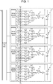
- FIG. 1 is a diagram illustrating a configuration of power supply system 1 according to an embodiment of the present invention.
- Power supply system 1 includes a plurality of power storage stacks (in FIG. 1 , first power storage stack 10 to fourth power storage stack 40) and controlling circuit 50.
- First power storage stack 10 includes first power storage module M1, first voltage detection circuit 11, first power source circuit 12, a plurality of switches S10 to S19, and first discharge circuit 13.
- First power storage module M1 is formed by connecting a plurality of cells E1 to E5) in series.
- a lithium-ion battery cell a nickel-metal hydride battery cell, a lead battery cell, an electric double layer capacitor cell, a lithium-ion capacitor cell, or the like can be used.
- a lithium-ion battery cell nominal voltage: 3.6V to 3.7V
- First voltage detection circuit 11 is connected to the respective nodes of the plurality of cells E1 to E5 connected in series by a plurality of voltage lines. First voltage detection circuit 11 then detects a voltage between two adjacent voltage lines to detect the voltage of each of the cells E1 to E5.
- First voltage detection circuit 11 is constituted by, for example, an application specific integrated circuit (ASIC).
- First voltage detection circuit 11 includes a multiplexer and an analog-to-digital (A/D) converter (not illustrated).
- the multiplexer outputs the respective voltage values of the plurality of cells E1 to E5 to the A/D converter in a predetermined order.
- the A/D converter converts an analog signal, input from the multiplexer, into a digital signal.
- First power source circuit 12 steps down the voltage across first power storage module M1 to charge one of the plurality of cells E1 to E5.
- FIG. 1 illustrates an example in which first power source circuit 12 is constituted by an insulated flyback DC-to-DC (DC/DC) converter.
- the insulated flyback DC/DC converter includes first transformer T1, first switch S1, and first diode D1.
- first transformer T1 In the insulated flyback DC/DC converter, a primary winding and a secondary winding of first transformer T1 are connected in opposite polarities.
- first power source circuit 12 is not limited to the insulated flyback DC/DC converter, but may have any configuration so long as being an insulated power source circuit capable of stepping down a voltage across first power storage module M1 and outputting the reduced voltage.
- an insulated forward DC/DC converter and the like are known in addition to the insulated flyback DC/DC converter described above.
- Both ends of the primary winding of first transformer T1 are connected to both ends of first power storage module M1.
- First switch S1 is inserted between one end of the primary winding and one end of first power storage module M1.
- First diode D1 for rectification is connected to one end of the secondary winding of first transformer T1.
- the secondary winding of first transformer T1 and both ends of any of the plurality of cells E1 to E5 are connected via each of the plurality of switches S10 to S19.
- a voltage line is connected to the respective nodes of the plurality of cells E1 to E5.
- a first voltage line, a third voltage line, and a fifth voltage line are coupled by first positive electrode wiring Lp1
- a second voltage line, a fourth voltage line, and a sixth voltage line are coupled by first negative electrode wiring Lp1.
- Tenth switch S10 to sixteenth switch S16 are inserted into the first voltage line to the sixth voltage line, respectively.
- the terminal on the current output side of the secondary winding of first transformer T1 and first positive electrode wiring Lp1 are connected via sixteenth switch S16, and the terminal on the current output side of the secondary winding and first negative electrode wiring Lm1 are connected seventeenth switch S17.
- the terminal on the current input side of the secondary winding of first transformer T1 and first positive electrode wiring Lp1 are connected via nineteenth switch S19, and the terminal on the current input side of the secondary winding and first negative electrode wiring Lm1 are connected via eighteenth switch S18.
- First discharge circuit 13 includes fifth switch S5 and first resistor R1 connected in series. Fifth switch S5 and first resistor R1 connected in series are connected between both ends of first power storage module M1.
- First power storage module M1 to fourth power storage module M4 are connected in series to form one power storage unit.
- each of power storage modules M1 to M4 includes five cells connected in series, so that a series circuit with a total of 20 cells is formed.
- a number of cells in series is increased.
- a series circuit with a total of 100 cells may be formed, for example, in a case where a motor requiring a high voltage (e.g., about 400V) is used.
- Typical power storage modules each including five to twenty cells connected in series are connected in series to form one power storage unit.
- the present exemplary embodiment illustrates an example of the power storage module including five cells connected in series, the number of cells included in the power storage module is preferably designed in accordance with a withstand voltage of an ASIC or a power source circuit.
- a configuration in which the power storage unit is excluded from power supply system 1 is collectively referred to as a management device.
- Controlling circuit 50 controls the whole of power supply system 1.
- Controlling circuit 50 is constituted by a microprocessor, for example.
- Controlling circuit 50 is connected to a plurality of voltage detection circuits 11 to 41 through communication lines. More specifically, controlling circuit 50 and the plurality of voltage detection circuits 11 to 41 are connected by digital communication via insulation circuits such as photocouplers. Due to the need for voltage detection circuits 11 to 41 to detect the voltages of the plurality of cells connected in series, it is necessary to increase the voltage.
- controlling circuit 50 is normally operated by being supplied with power from a lead battery of 12V. In order to absorb this voltage difference, voltage detection circuits 11 to 41 and control circuit 50 must be insulated.
- Controlling circuit 50 estimates a state of charge (SOC) and a state of health (SOH) of each of the plurality of cells E1 to E20.
- the SOC can be estimated by, for example, an open circuit voltage (OCV) method or a current integration method.
- OCV open circuit voltage
- the SOH is defined as the ratio of the current full charge capacity to the initial full charge capacity, and a lower value (closer to 0%) indicates that more degradation progresses.
- the SOH can be estimated on the basis of the correlation with internal resistance.
- the internal resistance can be estimated by dividing a voltage drop, generated when a predetermined current is allowed to pass through the battery for a predetermined time, by the current.
- the degradation of the battery progresses as a number of times of charge and discharge increases.
- the degradation of the battery also depends on the individual difference and use environment. Therefore, as the use period becomes longer, basically, variations in the capacities of the plurality of cells E1 to E20 increase.
- Controlling circuit 50 acquires the voltage values of respective cells E1 to E20 from the plurality of voltage detection circuits 11 to 44 and performs an equalizing process. Controlling circuit 50 equalizes voltages among the plurality of cells forming one power storage module by using power source circuit 12 to 42 (active balancing). Control circuit 50 equalizes voltages among the plurality of power storage modules M1 to M4 by using discharge circuits 13 to 43 (passive balancing).
- the active balancing of first power storage module M1 will be described below.
- the capacity of the least capacity cell among the plurality of cells E1 to E5 is charged to the capacity of the most capacity cell.
- the capacity of the cell with the smallest capacity reaches the capacity of the cell with the largest capacity, the same control is repeated until the capacities of all the cells match substantially.
- Controlling circuit 50 acquires/estimates the OCV/SOC of the plurality of cells E1 to E5, and specifies the cell having the lowest OCV/SOC.
- Controlling circuit 50 controls two switches, sixteenth switch S 16/seventeenth switch S17 and eighteenth switch S18/nineteenth switch S19 each inserted into two voltage lines connected to nodes at both ends of the cell, to be turned on. For example, in a case where first cell E1 is charged, tenth switch S10, eleventh switch S11, sixteenth switch S16, and eighteenth switch S18 are controlled to be turned on. In a case where second cell E2 is charged, eleventh switch S11, twelfth switch S12, seventeenth switch S17, and nineteenth switch S19 are controlled to be turned on.
- Controlling circuit 50 may be configured to perform pulse width modulation (PWM) control on first switch S1.
- First power source circuit 12 receives the voltage across first power storage module M1, steps down the received voltage across first power storage module M1, and outputs an output voltage.
- PWM pulse width modulation
- First power source circuit 12 receives the voltage across first power storage module M1, steps down the received voltage across first power storage module M1, and outputs an output voltage.
- a charging current flows in accordance the voltage of the cell, and the amount of the charging current can be adjusted by performing the PWM control on first switch S1.
- the output of first power source circuit 12 can be adjusted by the winding ratio of the primary winding and the secondary winding of first transformer T1 and the duty ratio of first switch S1.
- the charging control various methods can be employed.
- CC-CV constant-current constant-voltage system
- any configuration may be adopted so long as the method can charge a target cell by using the voltage across first power storage module M1.
- controlling circuit 50 can substantially match the OCV/SOC among the plurality of cells E1 to E5.
- a rechargeable amount/dischargeable amount may be used instead of OCV/SOC among the plurality of cells E1 to E5.
- the above active balancing is also performed in second power storage module M2 to fourth power storage module M4.
- controlling circuit 50 can perform the active balancing and the passive balancing described below simultaneously in parallel.
- Controlling circuit 50 estimates the OCV/SOC of each of the plurality of power storage modules M1 to M4, and specifies the power storage module having the lowest OCV/SOC. Controlling circuit 50 determines the respective discharge times for the other plurality of power storage modules in order to match the OCVs/SOCs of the other plurality of power storage modules to the power storage module having the lowest OCV/SOC. Controlling circuit 50 determines each discharge time on the basis of the discharge capacity based on the difference between the current OCV/SOC and the target OCV/SOC for equalization in each power storage module and the resistance value of each of the resistors R1-R4 for discharge. Note that the resistance values of the plurality of resistors R1 to R4 are assumed to be the same.
- Controlling circuit 50 controls the on/off of discharge switches S5 to S8 in the other plurality of power storage modules on the basis of the respective determined discharge times. In the power storage stack with the discharge switch in the on-state, a current flows from the power storage module to the discharge resistor, thereby lowering the OCV/SOC of the power storage module.
- Controlling circuit 50 transmits a control signal for instructing the on/off of first switch S1, fifth switch S5, and tenth switch S10 to nineteenth switch S19, to first voltage detection circuit 11, transmits a control signal for instructing the on/off of second switch S2, sixth switch S6, and twentieth switch S20 to twenty-ninth switch S29, to second voltage detection circuit 21, transmits a control signal for instructing the on/off of third switch S3, seventh switch S7, and thirtieth switch S30 to thirty-ninth switch S39, to third voltage detection circuit 31, and transmits a control signal for instructing the on/off of fourth switch S4, eighth switch S8 and fortieth switch S40 to forty-ninth switch S49, to fourth voltage detection circuit 41.
- First voltage detection circuit 11 to fourth voltage detection circuit 41 control the on/off of switches S1 to S49 on the basis of the control signals received from controlling circuit 50.
- FIG. 2 is a diagram illustrating a configuration of power supply system 1 according to Comparative Example 1.
- Comparative Example 1 is an example of performing the equalizing process only by the active balancing.
- discharge circuits 13 to 43 are not provided.
- one power source circuit 12 is provided for the plurality of power storage modules M1 to M4. Odd-numbered voltage lines are connected to positive electrode wiring Lp1, and even-numbered voltage lines are connected to negative electrode wiring Lm1.
- FIG. 3 is a diagram illustrating a configuration of power supply system 1 according to Comparative Example 2.
- Comparative Example 2 is an example of performing the equalizing process only by the passive balancing.
- first power source circuit 12 to fourth power source circuit 42 and tenth switch S10 to forty-ninth switch S49 are not provided.
- one discharge circuit is provided for each cell. Specifically, first discharge switch S51 and first discharge resistor R51 are connected in series to both ends of first cell E1, second discharge switch S52 and second discharge resistor R52 are connected in series to both ends of second cell E2,..., and twentieth discharge switch S85 and twentieth resistor R85 are connected to both ends of twentieth cell E20.
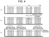
- FIGS. 4(a) to 4(c) are diagrams illustrating an example of the equalizing process in power supply system 1 according to the exemplary embodiment of the present invention.
- FIG. 4(a) is a diagram illustrating the states of capacities of cells E1 to E20 before the equalizing process.
- the capacity of thirteenth cell E13 has been reduced. Due to aging degradation, individual variation, or the like, a cell with a large self-discharge amount may be generated.
- Thirteenth cell E13 is a cell having a larger self-discharge amount than other cells E1 to E12 and E14 to E20.
- Controlling circuit 50 performs the active balancing in third power storage stack 30. Specifically, controlling circuit 50 instructs third voltage detection circuit 31 to charge thirteenth cell E13 by using third power source circuit 32. Third voltage detection circuit 31 performs the PWM control on third switch S3 by controlling thirty-second switch S32, thirty-third switch S33, thirty-sixth switch S36, and thirty-eighth switch S38 to be turned on.
- FIG. 4(b) is a diagram illustrating the states of the capacities of cells E1 to E20 after completion of active cell balancing in third power storage stack 30. Since the active cell balancing has been completed in third power storage module M3, the capacities of other cells E10 to E12 and E13 to E15 in third power storage module M3 decrease with the charging of thirteenth cell E13.
- Controlling circuit 50 performs the passive balancing among first power storage stack 10 and fourth power storage stack 40. Specifically, controlling circuit 50 instructs first voltage detection circuit 11, second voltage detection circuit 21, and fourth voltage detection circuit 41 to discharge the capacities of first power storage module M1, second power storage module M2, and fourth power storage module M4 to the capacity of third power storage module M3. First voltage detection circuit 11, second voltage detection circuit 21, and fourth voltage detection circuit 41 control fifth switch S5, sixth switch S6, and eighth switch S8 to be turned on, respectively, to discharge the capacities of first power storage module M1, second power storage module M2, and fourth power storage module M4.
- FIG. 4(c) is a diagram illustrating the states of the capacities of cells E1 to E20 after completion of the passive balancing among first power storage stack 10 and fourth power storage stack 40.
- the capacities of all cells E1 to E20 are substantially the same.
- it is necessary to discharge the capacities of other cells E1 to E12 and E14 to E20 to the capacity of thirteenth cell E13 illustrated in FIG. 4(a) which is inefficient as compared to the equalizing process according to the present exemplary embodiment.
- the active balancing is performed among the plurality of cells in each power storage stack, and the passive balancing is performed among the plurality of power storage modules among the plurality of power storage stacks. It is thereby possible to improve the power efficiency while preventing the complication of the component configuration.
- the wiring is complicated.
- the active balancing is completed in one power storage stack, it is possible to mount the power source circuit and wiring between the power source circuit and the plurality of cells on a substrate in the power storage stack. Therefore, the configuration can be simplified.
- the wiring between the power source circuit and the plurality of cells needs to be placed outside the power storage stack, which complicates the wiring and increases the length of the wiring.
- one voltage detection circuit is mounted on one power storage stack.
- a configuration in which a plurality of voltage detection circuits are mounted on one power storage stack is also possible.
- two voltage detection circuits may be mounted on a power storage stack including 20 cells connected in series, and each voltage detection circuit may detect a voltage corresponding to 10 cells.
- the active cell balancing is performed for each of a plurality of cells (ten in this example) managed by one voltage detection circuit.
- two independent active balancing operations are performed in one power storage stack.
- a management device provided with: a plurality of power source circuits (12, 22, 32, 42) connected respectively to a plurality of series cell groups (M1, M2, M3, M4) each including a plurality of cells (E1 to E5, E6 to E10, E11 to E5, E16 to E20) connected in series, the plurality of power source circuits (12, 22, 32, 42) each being configured to be able to selectively charge any one of the plurality of cells (E1 to E5, E6 to E10, E11 to E5, E16 to E20) included in each of the plurality of series cell groups (M1, M2, M3, M4) by using a voltage across each of the plurality of series cell groups (M1, M2, M3, M4); a plurality of discharge circuits (13, 23, 33, 43) connected respectively to the plurality of series cell groups (M1, M2, M3, M4), the plurality of discharge circuits (13, 23, 33, 43) each being configured to be able to discharge a capacity stored in each of the plurality of series cell groups (
- Controlling circuit (50) equalizes states of the plurality of cells (E1 to E5, E6 to E10, E11 to E5, E16 to E20) included in series cell group (M1, M2, M3, M4) by using the plurality of power source circuits (12, 22, 32, 42), and equalizes states of the plurality of series cell groups (M1, M2, M3, M4) by using the plurality of discharge circuits (13, 23, 33, 43).
- discharge circuit (13, 23, 33, 43) includes: one resistor (R1, R2, R3, R4) that discharges the capacity stored in series cell group (M1, M2, M3, M4); and a switch (S5, S6, S7, S8) connected between series cell group (M1, M2, M3, M4) and one resistor (R1, R2, R3, R4).
- controlling circuit (50) performs a process of equalization among the plurality of cells (E1 to E5, E6 to E10, E11 to E15, E16 to E20) forming series cell group (M1, M2, M3, M4) and a process of equalization among the plurality of series cell groups (M1, M2, M3, M4) in parallel.
- the time required for the equalizing process can be shortened.
- a power supply system (1) provided with: a power storage unit in which the plurality of series cell groups (M1, M2, M3, M4) are connected in series; and the management device according to any one of items 1 to 3 that manages the power storage unit.
Landscapes
- Engineering & Computer Science (AREA)
- Power Engineering (AREA)
- Manufacturing & Machinery (AREA)
- Chemical & Material Sciences (AREA)
- Chemical Kinetics & Catalysis (AREA)
- Electrochemistry (AREA)
- General Chemical & Material Sciences (AREA)
- Microelectronics & Electronic Packaging (AREA)
- Charge And Discharge Circuits For Batteries Or The Like (AREA)
- Secondary Cells (AREA)
Abstract
Description
- The present invention relates to a management device that manages the state of a power storage unit and a power supply system.
- In recent years, hybrid vehicles (HV), plug-in hybrid vehicles (PHV), and electric vehicles (EV) have become popular. These cars are equipped with secondary batteries as key devices. Nickel-metal hydride batteries and lithium-ion batteries are widely used as automotive secondary batteries. Lithium-ion batteries with a high energy density are expected to become more widely used in the future.
- Lithium-ion batteries require stricter voltage control than other types of batteries because the normal range is close to the no-use range. Generally, in a lithium-ion battery, an equalizing process for equalizing voltages among a plurality of cells connected in series is performed from the viewpoint of maintaining power efficiency and ensuring safety (e.g., see PTL 1).
- A passive method is a mainstream for the equalizing process. In the passive method, discharge resistors are connected to a plurality of cells connected in serial, respectively, and the cells other than the lowest-voltage cell are discharged so as to match the voltages of the other cells with the voltage of the lowest-voltage cell.
- As another method of the equalizing process, there is an active method. In the active method, a charging circuit is provided, and among a plurality of cells connected in series, the cells other than the highest-voltage cell are charged so as to match the voltages of the other cells with the voltage of the highest-voltage cell.
- PTL 1: Unexamined Japanese Patent Publication No.
2013-223378 - In the passive method, a part of the energy stored in the cell needs to be discarded for equalization, and the power efficiency is lowered. Heat is generated when a current flows through the discharge resistor. On the other hand, in the active method, since a charging circuit for charging each cell is required, the component configuration is complicated and the cost is increased.
- The present invention is made in view of the above situation, and an object of the present invention is to provide a technique for improving power efficiency while preventing the complication of a component configuration in a process of equalization among a plurality of cells connected in series.
- In order to solve the above problems, a management device according to an aspect of the present invention is a management device provided with: a plurality of power source circuits connected respectively to a plurality of series cell groups each including a plurality of cells connected in series, the plurality of power source circuits each being configured to be able to selectively charge any one of the plurality of cells included in each of the series cell groups by using a voltage across each of the plurality of series cell groups; a plurality of discharge circuits connected respectively to the plurality of series cell groups, the plurality of discharge circuits each being configured to be able to discharge a capacity stored in each of the plurality of series cell groups; a voltage detection circuit that detects each of voltages of the plurality of cells included in each of the plurality of series cell groups; and a controlling circuit that acquires a voltage value of each of the plurality of cells from the voltage detection circuit and controls the plurality of power source circuits and the plurality of discharge circuits. The controlling circuit equalizes the states of the plurality of cells included in each of the plurality of series cell groups by using the plurality of power source circuits, and equalizes the states of the plurality of series cell groups by using the plurality of discharge circuits.
- Note that any combination of the above configuration elements and the expression of the present invention converted among methods, apparatuses, systems, and the like are also effective as aspects of the present invention.
- According to the present invention, in the process of equalization among a plurality of cells connected in series, it is possible to improve the power efficiency while preventing the complication of the component configuration.
-
-
FIG. 1 is a diagram illustrating a configuration of a power supply system according to an embodiment of the present invention. -
FIG. 2 is a diagram illustrating a configuration of a power supply system according to Comparative Example 1. -
FIG. 3 is a diagram illustrating a configuration of a power supply system according to Comparative Example 2. -
FIGS. 4(a) to 4(c) are diagrams illustrating an example of an equalizing process in the power supply system according to the embodiment of the present invention. -
FIG. 1 is a diagram illustrating a configuration ofpower supply system 1 according to an embodiment of the present invention.Power supply system 1 includes a plurality of power storage stacks (inFIG. 1 , firstpower storage stack 10 to fourth power storage stack 40) and controllingcircuit 50. Firstpower storage stack 10 includes first power storage module M1, firstvoltage detection circuit 11, firstpower source circuit 12, a plurality of switches S10 to S19, andfirst discharge circuit 13. - First power storage module M1 is formed by connecting a plurality of cells E1 to E5) in series. As the cell, a lithium-ion battery cell, a nickel-metal hydride battery cell, a lead battery cell, an electric double layer capacitor cell, a lithium-ion capacitor cell, or the like can be used. Hereinafter, in the present specification, an example of using a lithium-ion battery cell (nominal voltage: 3.6V to 3.7V) is assumed.
- First
voltage detection circuit 11 is connected to the respective nodes of the plurality of cells E1 to E5 connected in series by a plurality of voltage lines. Firstvoltage detection circuit 11 then detects a voltage between two adjacent voltage lines to detect the voltage of each of the cells E1 to E5. Firstvoltage detection circuit 11 is constituted by, for example, an application specific integrated circuit (ASIC). Firstvoltage detection circuit 11 includes a multiplexer and an analog-to-digital (A/D) converter (not illustrated). The multiplexer outputs the respective voltage values of the plurality of cells E1 to E5 to the A/D converter in a predetermined order. The A/D converter converts an analog signal, input from the multiplexer, into a digital signal. - First
power source circuit 12 steps down the voltage across first power storage module M1 to charge one of the plurality of cells E1 to E5.FIG. 1 illustrates an example in which firstpower source circuit 12 is constituted by an insulated flyback DC-to-DC (DC/DC) converter. The insulated flyback DC/DC converter includes first transformer T1, first switch S1, and first diode D1. In the insulated flyback DC/DC converter, a primary winding and a secondary winding of first transformer T1 are connected in opposite polarities. Note that firstpower source circuit 12 is not limited to the insulated flyback DC/DC converter, but may have any configuration so long as being an insulated power source circuit capable of stepping down a voltage across first power storage module M1 and outputting the reduced voltage. As this type of power source circuit, an insulated forward DC/DC converter and the like are known in addition to the insulated flyback DC/DC converter described above. - Both ends of the primary winding of first transformer T1 are connected to both ends of first power storage module M1. First switch S1 is inserted between one end of the primary winding and one end of first power storage module M1. First diode D1 for rectification is connected to one end of the secondary winding of first transformer T1.
- The secondary winding of first transformer T1 and both ends of any of the plurality of cells E1 to E5 are connected via each of the plurality of switches S10 to S19. A voltage line is connected to the respective nodes of the plurality of cells E1 to E5. A first voltage line, a third voltage line, and a fifth voltage line are coupled by first positive electrode wiring Lp1, and a second voltage line, a fourth voltage line, and a sixth voltage line are coupled by first negative electrode wiring Lp1. Tenth switch S10 to sixteenth switch S16 are inserted into the first voltage line to the sixth voltage line, respectively.
- The terminal on the current output side of the secondary winding of first transformer T1 and first positive electrode wiring Lp1 are connected via sixteenth switch S16, and the terminal on the current output side of the secondary winding and first negative electrode wiring Lm1 are connected seventeenth switch S17. The terminal on the current input side of the secondary winding of first transformer T1 and first positive electrode wiring Lp1 are connected via nineteenth switch S19, and the terminal on the current input side of the secondary winding and first negative electrode wiring Lm1 are connected via eighteenth switch S18.
-
First discharge circuit 13 includes fifth switch S5 and first resistor R1 connected in series. Fifth switch S5 and first resistor R1 connected in series are connected between both ends of first power storage module M1. - Configurations of second
power storage stack 20, thirdpower storage stack 30, and fourthpower storage stack 40 are the same as that of the firstpower storage stack 10, and hence descriptions thereof will be omitted. First power storage module M1 to fourth power storage module M4 are connected in series to form one power storage unit. In the example illustrated inFIG. 1 , each of power storage modules M1 to M4 includes five cells connected in series, so that a series circuit with a total of 20 cells is formed. In a case where a high voltage motor is used, a number of cells in series is increased. A series circuit with a total of 100 cells may be formed, for example, in a case where a motor requiring a high voltage (e.g., about 400V) is used. Typically, eight or more power storage modules each including five to twenty cells connected in series are connected in series to form one power storage unit. Although the present exemplary embodiment illustrates an example of the power storage module including five cells connected in series, the number of cells included in the power storage module is preferably designed in accordance with a withstand voltage of an ASIC or a power source circuit. In the present exemplary embodiment, a configuration in which the power storage unit is excluded frompower supply system 1 is collectively referred to as a management device. - Controlling
circuit 50 controls the whole ofpower supply system 1. Controllingcircuit 50 is constituted by a microprocessor, for example. Controllingcircuit 50 is connected to a plurality ofvoltage detection circuits 11 to 41 through communication lines. More specifically, controllingcircuit 50 and the plurality ofvoltage detection circuits 11 to 41 are connected by digital communication via insulation circuits such as photocouplers. Due to the need forvoltage detection circuits 11 to 41 to detect the voltages of the plurality of cells connected in series, it is necessary to increase the voltage. On the other hand, controllingcircuit 50 is normally operated by being supplied with power from a lead battery of 12V. In order to absorb this voltage difference,voltage detection circuits 11 to 41 andcontrol circuit 50 must be insulated. - Controlling
circuit 50 estimates a state of charge (SOC) and a state of health (SOH) of each of the plurality of cells E1 to E20. The SOC can be estimated by, for example, an open circuit voltage (OCV) method or a current integration method. The SOH is defined as the ratio of the current full charge capacity to the initial full charge capacity, and a lower value (closer to 0%) indicates that more degradation progresses. The SOH can be estimated on the basis of the correlation with internal resistance. The internal resistance can be estimated by dividing a voltage drop, generated when a predetermined current is allowed to pass through the battery for a predetermined time, by the current. There is a relationship in which the internal resistance decreases as the temperature increases, and there is a relationship in which the internal resistance increases as the degradation of the battery progresses. The degradation of the battery progresses as a number of times of charge and discharge increases. The degradation of the battery also depends on the individual difference and use environment. Therefore, as the use period becomes longer, basically, variations in the capacities of the plurality of cells E1 to E20 increase. - Controlling
circuit 50 acquires the voltage values of respective cells E1 to E20 from the plurality ofvoltage detection circuits 11 to 44 and performs an equalizing process. Controllingcircuit 50 equalizes voltages among the plurality of cells forming one power storage module by usingpower source circuit 12 to 42 (active balancing).Control circuit 50 equalizes voltages among the plurality of power storage modules M1 to M4 by usingdischarge circuits 13 to 43 (passive balancing). - The active balancing of first power storage module M1 will be described below. In the active balancing, the capacity of the least capacity cell among the plurality of cells E1 to E5 is charged to the capacity of the most capacity cell. When the capacity of the cell with the smallest capacity reaches the capacity of the cell with the largest capacity, the same control is repeated until the capacities of all the cells match substantially.
- Controlling
circuit 50 acquires/estimates the OCV/SOC of the plurality of cells E1 to E5, and specifies the cell having the lowest OCV/SOC. Controllingcircuit 50 controls two switches,sixteenth switch S 16/seventeenth switch S17 and eighteenth switch S18/nineteenth switch S19 each inserted into two voltage lines connected to nodes at both ends of the cell, to be turned on. For example, in a case where first cell E1 is charged, tenth switch S10, eleventh switch S11, sixteenth switch S16, and eighteenth switch S18 are controlled to be turned on. In a case where second cell E2 is charged, eleventh switch S11, twelfth switch S12, seventeenth switch S17, and nineteenth switch S19 are controlled to be turned on. - Controlling
circuit 50 may be configured to perform pulse width modulation (PWM) control on first switch S1. Firstpower source circuit 12 receives the voltage across first power storage module M1, steps down the received voltage across first power storage module M1, and outputs an output voltage. When the cell is connected to the output side of firstpower source circuit 12, a charging current flows in accordance the voltage of the cell, and the amount of the charging current can be adjusted by performing the PWM control on first switch S1. In this way, the output of firstpower source circuit 12 can be adjusted by the winding ratio of the primary winding and the secondary winding of first transformer T1 and the duty ratio of first switch S1. As the charging control, various methods can be employed. As the charging control, for example, a constant-current constant-voltage system (CC-CV) is typically known, but any configuration may be adopted so long as the method can charge a target cell by using the voltage across first power storage module M1. - As described above, by repeating the control of charging the cell having the lowest OCV/SOC to the OCV/SOC of the cell with the highest OCV/SOC, controlling
circuit 50 can substantially match the OCV/SOC among the plurality of cells E1 to E5. As a target value for equalization, a rechargeable amount/dischargeable amount may be used instead of OCV/SOC among the plurality of cells E1 to E5. The above active balancing is also performed in second power storage module M2 to fourth power storage module M4. - Since the active balancing described above is an energy transfer among the cells in each power storage module, the voltage across each power storage module is essentially unchanged during the active balancing. Thus, controlling
circuit 50 can perform the active balancing and the passive balancing described below simultaneously in parallel. - Controlling
circuit 50 estimates the OCV/SOC of each of the plurality of power storage modules M1 to M4, and specifies the power storage module having the lowest OCV/SOC. Controllingcircuit 50 determines the respective discharge times for the other plurality of power storage modules in order to match the OCVs/SOCs of the other plurality of power storage modules to the power storage module having the lowest OCV/SOC. Controllingcircuit 50 determines each discharge time on the basis of the discharge capacity based on the difference between the current OCV/SOC and the target OCV/SOC for equalization in each power storage module and the resistance value of each of the resistors R1-R4 for discharge. Note that the resistance values of the plurality of resistors R1 to R4 are assumed to be the same. Controllingcircuit 50 controls the on/off of discharge switches S5 to S8 in the other plurality of power storage modules on the basis of the respective determined discharge times. In the power storage stack with the discharge switch in the on-state, a current flows from the power storage module to the discharge resistor, thereby lowering the OCV/SOC of the power storage module. - Controlling
circuit 50 transmits a control signal for instructing the on/off of first switch S1, fifth switch S5, and tenth switch S10 to nineteenth switch S19, to firstvoltage detection circuit 11, transmits a control signal for instructing the on/off of second switch S2, sixth switch S6, and twentieth switch S20 to twenty-ninth switch S29, to secondvoltage detection circuit 21, transmits a control signal for instructing the on/off of third switch S3, seventh switch S7, and thirtieth switch S30 to thirty-ninth switch S39, to thirdvoltage detection circuit 31, and transmits a control signal for instructing the on/off of fourth switch S4, eighth switch S8 and fortieth switch S40 to forty-ninth switch S49, to fourthvoltage detection circuit 41. Firstvoltage detection circuit 11 to fourthvoltage detection circuit 41 control the on/off of switches S1 to S49 on the basis of the control signals received from controllingcircuit 50. -
FIG. 2 is a diagram illustrating a configuration ofpower supply system 1 according to Comparative Example 1. Comparative Example 1 is an example of performing the equalizing process only by the active balancing. In Comparative Example 1, dischargecircuits 13 to 43 are not provided. In Comparative Example 1, onepower source circuit 12 is provided for the plurality of power storage modules M1 to M4. Odd-numbered voltage lines are connected to positive electrode wiring Lp1, and even-numbered voltage lines are connected to negative electrode wiring Lm1. -
FIG. 3 is a diagram illustrating a configuration ofpower supply system 1 according to Comparative Example 2. Comparative Example 2 is an example of performing the equalizing process only by the passive balancing. In Comparative Example 2, firstpower source circuit 12 to fourthpower source circuit 42 and tenth switch S10 to forty-ninth switch S49 are not provided. In Comparative Example 2, one discharge circuit is provided for each cell. Specifically, first discharge switch S51 and first discharge resistor R51 are connected in series to both ends of first cell E1, second discharge switch S52 and second discharge resistor R52 are connected in series to both ends of second cell E2,..., and twentieth discharge switch S85 and twentieth resistor R85 are connected to both ends of twentieth cell E20. -
FIGS. 4(a) to 4(c) are diagrams illustrating an example of the equalizing process inpower supply system 1 according to the exemplary embodiment of the present invention.FIG. 4(a) is a diagram illustrating the states of capacities of cells E1 to E20 before the equalizing process. InFIG. 4(a) , the capacity of thirteenth cell E13 has been reduced. Due to aging degradation, individual variation, or the like, a cell with a large self-discharge amount may be generated. Thirteenth cell E13 is a cell having a larger self-discharge amount than other cells E1 to E12 and E14 to E20. - Controlling
circuit 50 performs the active balancing in thirdpower storage stack 30. Specifically, controllingcircuit 50 instructs thirdvoltage detection circuit 31 to charge thirteenth cell E13 by using thirdpower source circuit 32. Thirdvoltage detection circuit 31 performs the PWM control on third switch S3 by controlling thirty-second switch S32, thirty-third switch S33, thirty-sixth switch S36, and thirty-eighth switch S38 to be turned on. -
FIG. 4(b) is a diagram illustrating the states of the capacities of cells E1 to E20 after completion of active cell balancing in thirdpower storage stack 30. Since the active cell balancing has been completed in third power storage module M3, the capacities of other cells E10 to E12 and E13 to E15 in third power storage module M3 decrease with the charging of thirteenth cell E13. - Controlling
circuit 50 performs the passive balancing among firstpower storage stack 10 and fourthpower storage stack 40. Specifically, controllingcircuit 50 instructs firstvoltage detection circuit 11, secondvoltage detection circuit 21, and fourthvoltage detection circuit 41 to discharge the capacities of first power storage module M1, second power storage module M2, and fourth power storage module M4 to the capacity of third power storage module M3. Firstvoltage detection circuit 11, secondvoltage detection circuit 21, and fourthvoltage detection circuit 41 control fifth switch S5, sixth switch S6, and eighth switch S8 to be turned on, respectively, to discharge the capacities of first power storage module M1, second power storage module M2, and fourth power storage module M4. -
FIG. 4(c) is a diagram illustrating the states of the capacities of cells E1 to E20 after completion of the passive balancing among firstpower storage stack 10 and fourthpower storage stack 40. InFIG. 4(c) , the capacities of all cells E1 to E20 are substantially the same. When the equalizing process using only the passive balancing illustrated in Comparative Example 2 is performed, it is necessary to discharge the capacities of other cells E1 to E12 and E14 to E20 to the capacity of thirteenth cell E13 illustrated inFIG. 4(a) , which is inefficient as compared to the equalizing process according to the present exemplary embodiment. - As described above, according to the present exemplary embodiment, the active balancing is performed among the plurality of cells in each power storage stack, and the passive balancing is performed among the plurality of power storage modules among the plurality of power storage stacks. It is thereby possible to improve the power efficiency while preventing the complication of the component configuration.
- In the method of performing the equalization only by the passive balancing as illustrated in Comparative Example 2, it is necessary to add the discharge resistor for each cell, and a number of components increases. Further, heat is generated when the capacity is discharged to the discharge resistor. In applications where a high voltage is required, the number of cells increases, and hence a loss due to equalizing discharge increases. In contrast, in the present exemplary embodiment, a loss due to the equalizing discharge can be reduced greatly.
- On the other hand, in the method of performing the equalization only by the active balancing as illustrated in Comparative Example 1, it is necessary to generate a voltage (e.g., about 5V) for charging one cell from the total voltage (e.g., about 400V) of the power storage unit, and
power source circuit 12 with a high withstand voltage is required. The use of components with the high withstand voltage increases the overall size of the circuit. - Further, due to the need for connecting all cells E1 to E20 to one
power source circuit 12, the wiring is complicated. Inpower supply system 1 according to the present exemplary embodiment, since the active balancing is completed in one power storage stack, it is possible to mount the power source circuit and wiring between the power source circuit and the plurality of cells on a substrate in the power storage stack. Therefore, the configuration can be simplified. On the other hand, in the method of performing the equalization only by the active balancing according to Comparative Example 1, the wiring between the power source circuit and the plurality of cells needs to be placed outside the power storage stack, which complicates the wiring and increases the length of the wiring. - The present invention has been described above on the basis of the exemplary embodiment. It will be understood by the persons of ordinary skill in the art that the exemplary embodiment is illustrative, that variations can be made on a combination of each configuration element and each processing process of the exemplary embodiment, and that such variations are within the scope of the present invention.
- In the above exemplary embodiment, an example in which one voltage detection circuit is mounted on one power storage stack has been described. In this regard, a configuration in which a plurality of voltage detection circuits are mounted on one power storage stack is also possible. For example, two voltage detection circuits may be mounted on a power storage stack including 20 cells connected in series, and each voltage detection circuit may detect a voltage corresponding to 10 cells. In this case, the active cell balancing is performed for each of a plurality of cells (ten in this example) managed by one voltage detection circuit. In this example, two independent active balancing operations are performed in one power storage stack.
- In the above exemplary embodiment, an example in which one discharge resistor is provided for each power storage stack has been described. In this regard, a number of discharge resistors is not limited to one, and the configuration in which a discharge resistor is added for each cell is not excluded.
- Note that the exemplary embodiment may be specified by the following items.
- A management device provided with: a plurality of power source circuits (12, 22, 32, 42) connected respectively to a plurality of series cell groups (M1, M2, M3, M4) each including a plurality of cells (E1 to E5, E6 to E10, E11 to E5, E16 to E20) connected in series, the plurality of power source circuits (12, 22, 32, 42) each being configured to be able to selectively charge any one of the plurality of cells (E1 to E5, E6 to E10, E11 to E5, E16 to E20) included in each of the plurality of series cell groups (M1, M2, M3, M4) by using a voltage across each of the plurality of series cell groups (M1, M2, M3, M4); a plurality of discharge circuits (13, 23, 33, 43) connected respectively to the plurality of series cell groups (M1, M2, M3, M4), the plurality of discharge circuits (13, 23, 33, 43) each being configured to be able to discharge a capacity stored in each of the plurality of series cell groups (M1, M2, M3, M4); voltage detection circuit (11, 21, 31, 41) that detects each of voltages of the plurality of cells (E1 to E5, E6 to E10, E11 to E5, E16 to E20) included in each of the plurality of series cell groups (M1, M2, M3, M4); and controlling circuit (50) that acquires a voltage value of each of the plurality of cells (E1 to E5, E6 to E10, E11 to E5, E16 to E20) from voltage detection circuit (11, 21, 31, 41) and controls the plurality of power source circuits (12, 22, 32, 42) and the plurality of discharge circuits (13, 23, 33, 43). Controlling circuit (50) equalizes states of the plurality of cells (E1 to E5, E6 to E10, E11 to E5, E16 to E20) included in series cell group (M1, M2, M3, M4) by using the plurality of power source circuits (12, 22, 32, 42), and equalizes states of the plurality of series cell groups (M1, M2, M3, M4) by using the plurality of discharge circuits (13, 23, 33, 43).
- According to the above, it is possible to achieve the equalizing process that improves the power efficiency while preventing the complication of the component configuration.
- The management device according to
item 1, in which discharge circuit (13, 23, 33, 43) includes: one resistor (R1, R2, R3, R4) that discharges the capacity stored in series cell group (M1, M2, M3, M4); and a switch (S5, S6, S7, S8) connected between series cell group (M1, M2, M3, M4) and one resistor (R1, R2, R3, R4). - According to the above, numbers of resistors for discharge and switches can be reduced.
- The management device according to
item 1 or 2, in which controlling circuit (50) performs a process of equalization among the plurality of cells (E1 to E5, E6 to E10, E11 to E15, E16 to E20) forming series cell group (M1, M2, M3, M4) and a process of equalization among the plurality of series cell groups (M1, M2, M3, M4) in parallel. - According to the above, the time required for the equalizing process can be shortened.
- A power supply system (1) provided with: a power storage unit in which the plurality of series cell groups (M1, M2, M3, M4) are connected in series; and the management device according to any one of
items 1 to 3 that manages the power storage unit. - According to the above, it is possible to achieve the equalizing process that improves the power efficiency while preventing the complication of the component configuration.
-
- 1:
- power supply system
- 10-40:
- power storage stack
- M1-M4:
- power storage module
- 11-41:
- voltage detection circuit
- 12-42:
- power source circuit
- 13-43:
- discharge circuit
- T1-T4:
- transformer
- D1-D4:
- diode
- Lp1-Lp4:
- positive electrode wiring
- Lm1-Lm4:
- negative electrode wiring
- S1-S49:
- switch
- R1-R85:
- resistor
- 50:
- controlling circuit
- E1-E20:
- cell
Claims (4)
- A management device comprising:a plurality of power source circuits connected respectively to a plurality of series cell groups each including a plurality of cells connected in series, the plurality of power source circuits each being configured to be able to selectively charge any one of the plurality of cells included in each of the plurality of series cell groups by using a voltage across each of the plurality of series cell groups;a plurality of discharge circuits connected respectively to the plurality of series cell groups, the plurality of discharge circuits each being configured to be able to discharge a capacity stored in each of the plurality of series cell groups;a voltage detection circuit that detects each of voltages of the plurality of cells included in each of the plurality of series cell groups; anda controlling circuit that acquires a voltage value of each of the plurality of cells from the voltage detection circuit and controls the plurality of power source circuits and the plurality of discharge circuits,wherein the controlling circuit equalizes states of the plurality of cells included in each of the plurality of series cell groups by using the plurality of power source circuits, and equalizes states of the plurality of series cell groups by using the plurality of discharge circuits.
- The management device according to claim 1, wherein each of the plurality of discharge circuits includes one resistor that discharges a capacity stored in each of the plurality of series cell groups, and a switch connected between each of the plurality of series cell groups and the one resistor.
- The management device according to claim 1 or 2, wherein the controlling circuit performs, a process of equalization among the plurality of cells forming the plurality of series cell groups, and a process of equalization among the plurality of series cell groups, in parallel.
- A power supply system comprising:a power storage unit in which the plurality of series cell groups are connected in series; andthe management device according to any one of claims 1 to 3 that manages the power storage unit.
Applications Claiming Priority (2)
| Application Number | Priority Date | Filing Date | Title |
|---|---|---|---|
| JP2017243128 | 2017-12-19 | ||
| PCT/JP2018/042205 WO2019123906A1 (en) | 2017-12-19 | 2018-11-15 | Management device and power supply system |
Publications (2)
| Publication Number | Publication Date |
|---|---|
| EP3731367A1 true EP3731367A1 (en) | 2020-10-28 |
| EP3731367A4 EP3731367A4 (en) | 2020-12-02 |
Family
ID=66992766
Family Applications (1)
| Application Number | Title | Priority Date | Filing Date |
|---|---|---|---|
| EP18889980.1A Withdrawn EP3731367A4 (en) | 2017-12-19 | 2018-11-15 | MANAGEMENT DEVICE AND POWER SUPPLY SYSTEM |
Country Status (5)
| Country | Link |
|---|---|
| US (1) | US11588185B2 (en) |
| EP (1) | EP3731367A4 (en) |
| JP (1) | JP7127064B2 (en) |
| CN (1) | CN111492557A (en) |
| WO (1) | WO2019123906A1 (en) |
Families Citing this family (9)
| Publication number | Priority date | Publication date | Assignee | Title |
|---|---|---|---|---|
| US12308673B2 (en) * | 2019-03-21 | 2025-05-20 | Hefei Gotion High-Tech Power Energy Co., Ltd. | Active equalizer circuit, battery management system, and power supply system |
| JP7260433B2 (en) * | 2019-07-24 | 2023-04-18 | 三洋電機株式会社 | Management device, power supply system |
| JP2021027706A (en) * | 2019-08-06 | 2021-02-22 | ダイハツ工業株式会社 | Battery system |
| EP4131707B1 (en) * | 2020-03-27 | 2025-07-30 | LG Innotek Co., Ltd. | Cell balancing module |
| JP7497466B2 (en) * | 2021-01-27 | 2024-06-10 | 武蔵精密工業株式会社 | Battery management device and battery device management method |
| FR3120277B1 (en) * | 2021-02-26 | 2023-05-12 | Otonohm | Device for storage and concomitant generation of at least one electrical voltage, and associated management method |
| WO2023021267A1 (en) * | 2021-08-20 | 2023-02-23 | Cirrus Logic International Semiconductor Limited | Cell balancing |
| GB2609998B (en) * | 2021-08-20 | 2024-01-17 | Cirrus Logic Int Semiconductor Ltd | Cell balancing |
| GB2615610B (en) * | 2022-02-15 | 2026-03-11 | Cirrus Logic Int Semiconductor Ltd | Cell balancing |
Family Cites Families (13)
| Publication number | Priority date | Publication date | Assignee | Title |
|---|---|---|---|---|
| SE527537C2 (en) * | 2004-04-26 | 2006-04-04 | X2 Technology I Vaexjoe Ab | Telescopic device |
| JP4130186B2 (en) * | 2004-11-12 | 2008-08-06 | 三洋電機株式会社 | Pack battery |
| JP2007300701A (en) | 2006-04-27 | 2007-11-15 | Sanyo Electric Co Ltd | Power supply device for vehicle |
| JP2010142039A (en) | 2008-12-12 | 2010-06-24 | Macnica Inc | Electrical energy storage device |
| JP5562617B2 (en) * | 2009-11-30 | 2014-07-30 | 三洋電機株式会社 | Equalizing device, battery system and electric vehicle |
| JP2011200095A (en) * | 2010-02-26 | 2011-10-06 | Sanyo Electric Co Ltd | Battery system |
| JP5484985B2 (en) * | 2010-03-29 | 2014-05-07 | 三洋電機株式会社 | Power supply device and vehicle equipped with this power supply device |
| US20120274283A1 (en) * | 2011-04-28 | 2012-11-01 | Van Lammeren Johannes | Battery cell-balancing method and apparatus |
| JP2013223378A (en) | 2012-04-18 | 2013-10-28 | Toyota Industries Corp | Battery equalization system and method |
| JP2015015777A (en) | 2013-07-03 | 2015-01-22 | ソニー株式会社 | Power storage device and method for controlling power storage device |
| CN104426175A (en) * | 2013-08-27 | 2015-03-18 | 通用电气公司 | System and method for battery management |
| KR102237034B1 (en) | 2014-02-18 | 2021-04-06 | 주식회사 실리콘웍스 | Balancing apparatus and the method supporting various balancing operation modes |
| DK179053B1 (en) | 2016-04-16 | 2017-09-18 | Lithium Balance As | Cell balancing method and system |
-
2018
- 2018-11-15 JP JP2019560874A patent/JP7127064B2/en active Active
- 2018-11-15 CN CN201880082038.4A patent/CN111492557A/en active Pending
- 2018-11-15 EP EP18889980.1A patent/EP3731367A4/en not_active Withdrawn
- 2018-11-15 US US16/954,389 patent/US11588185B2/en active Active
- 2018-11-15 WO PCT/JP2018/042205 patent/WO2019123906A1/en not_active Ceased
Also Published As
| Publication number | Publication date |
|---|---|
| JP7127064B2 (en) | 2022-08-29 |
| WO2019123906A1 (en) | 2019-06-27 |
| EP3731367A4 (en) | 2020-12-02 |
| JPWO2019123906A1 (en) | 2020-12-10 |
| CN111492557A (en) | 2020-08-04 |
| US20210083331A1 (en) | 2021-03-18 |
| US11588185B2 (en) | 2023-02-21 |
Similar Documents
| Publication | Publication Date | Title |
|---|---|---|
| EP3731367A1 (en) | Management device and power supply system | |
| KR101076786B1 (en) | Charge Equalization Apparatus for Series-Connected Battery String and Charge Equalization Method Thereof | |
| US11626741B2 (en) | Management device and power supply system | |
| EP3829023B1 (en) | Power supply system for balancing a plurality of cells connected in series | |
| CN101467328B (en) | Charge equalization equipment | |
| CN101606300B (en) | Balance charging equipment | |
| US9209630B2 (en) | Active battery cell balancing methods with variable duration discharge | |
| CN101849340B (en) | Battery management system with integrated voltage sensor and charge equalizer | |
| JP5175937B2 (en) | Uniform charging method and apparatus for series connected battery strings | |
| US9160179B2 (en) | Charging apparatus and charging method | |
| US20190176636A1 (en) | Battery management and balance circuit, battery system and method of charging the battery system | |
| CN106536261A (en) | Battery system and method for operating same | |
| JP7578686B2 (en) | Method for charging and/or discharging a rechargeable energy storage device - Patents.com | |
| JP2011188700A (en) | Power supply system, discharge control method, and discharge control program | |
| US9166431B2 (en) | Battery charge circuit | |
| JP7046750B2 (en) | Power supply system and management equipment | |
| US20200412134A1 (en) | Management device and electricity storage system | |
| US11095133B2 (en) | Simple battery and charger system | |
| WO2018038024A1 (en) | Power storage system | |
| KR20240145349A (en) | Battery pack |
Legal Events
| Date | Code | Title | Description |
|---|---|---|---|
| STAA | Information on the status of an ep patent application or granted ep patent |
Free format text: STATUS: THE INTERNATIONAL PUBLICATION HAS BEEN MADE |
|
| PUAI | Public reference made under article 153(3) epc to a published international application that has entered the european phase |
Free format text: ORIGINAL CODE: 0009012 |
|
| STAA | Information on the status of an ep patent application or granted ep patent |
Free format text: STATUS: REQUEST FOR EXAMINATION WAS MADE |
|
| 17P | Request for examination filed |
Effective date: 20200629 |
|
| AK | Designated contracting states |
Kind code of ref document: A1 Designated state(s): AL AT BE BG CH CY CZ DE DK EE ES FI FR GB GR HR HU IE IS IT LI LT LU LV MC MK MT NL NO PL PT RO RS SE SI SK SM TR |
|
| AX | Request for extension of the european patent |
Extension state: BA ME |
|
| A4 | Supplementary search report drawn up and despatched |
Effective date: 20201104 |
|
| RIC1 | Information provided on ipc code assigned before grant |
Ipc: H02J 7/00 20060101AFI20201029BHEP |
|
| DAV | Request for validation of the european patent (deleted) | ||
| DAX | Request for extension of the european patent (deleted) | ||
| STAA | Information on the status of an ep patent application or granted ep patent |
Free format text: STATUS: THE APPLICATION IS DEEMED TO BE WITHDRAWN |
|
| 18D | Application deemed to be withdrawn |
Effective date: 20210605 |