EP3729629B1 - A method for operating a plurality of chopper circuits - Google Patents
A method for operating a plurality of chopper circuits Download PDFInfo
- Publication number
- EP3729629B1 EP3729629B1 EP18815512.1A EP18815512A EP3729629B1 EP 3729629 B1 EP3729629 B1 EP 3729629B1 EP 18815512 A EP18815512 A EP 18815512A EP 3729629 B1 EP3729629 B1 EP 3729629B1
- Authority
- EP
- European Patent Office
- Prior art keywords
- time period
- switching
- chopper
- chopper circuit
- controllable
- Prior art date
- Legal status (The legal status is an assumption and is not a legal conclusion. Google has not performed a legal analysis and makes no representation as to the accuracy of the status listed.)
- Active
Links
Images






Classifications
-
- H—ELECTRICITY
- H02—GENERATION; CONVERSION OR DISTRIBUTION OF ELECTRIC POWER
- H02M—APPARATUS FOR CONVERSION BETWEEN AC AND AC, BETWEEN AC AND DC, OR BETWEEN DC AND DC, AND FOR USE WITH MAINS OR SIMILAR POWER SUPPLY SYSTEMS; CONVERSION OF DC OR AC INPUT POWER INTO SURGE OUTPUT POWER; CONTROL OR REGULATION THEREOF
- H02M5/00—Conversion of AC power input into AC power output, e.g. for change of voltage, for change of frequency, for change of number of phases
- H02M5/40—Conversion of AC power input into AC power output, e.g. for change of voltage, for change of frequency, for change of number of phases with intermediate conversion into DC
- H02M5/42—Conversion of AC power input into AC power output, e.g. for change of voltage, for change of frequency, for change of number of phases with intermediate conversion into DC by static converters
- H02M5/44—Conversion of AC power input into AC power output, e.g. for change of voltage, for change of frequency, for change of number of phases with intermediate conversion into DC by static converters using discharge tubes or semiconductor devices to convert the intermediate DC into AC
-
- H—ELECTRICITY
- H02—GENERATION; CONVERSION OR DISTRIBUTION OF ELECTRIC POWER
- H02J—ELECTRIC POWER NETWORKS; CIRCUIT ARRANGEMENTS OR SYSTEMS FOR SUPPLYING OR DISTRIBUTING ELECTRIC POWER; SYSTEMS FOR STORING ELECTRIC ENERGY
- H02J3/00—Circuit arrangements for AC mains or AC distribution networks
- H02J3/38—Arrangements for feeding a single network from two or more generators or sources in parallel; Arrangements for feeding already energised networks from additional generators or sources in parallel
- H02J3/381—Dispersed generators
-
- H—ELECTRICITY
- H02—GENERATION; CONVERSION OR DISTRIBUTION OF ELECTRIC POWER
- H02M—APPARATUS FOR CONVERSION BETWEEN AC AND AC, BETWEEN AC AND DC, OR BETWEEN DC AND DC, AND FOR USE WITH MAINS OR SIMILAR POWER SUPPLY SYSTEMS; CONVERSION OF DC OR AC INPUT POWER INTO SURGE OUTPUT POWER; CONTROL OR REGULATION THEREOF
- H02M1/00—Details of apparatus for conversion
- H02M1/32—Means for protecting converters other than automatic disconnection
-
- H—ELECTRICITY
- H02—GENERATION; CONVERSION OR DISTRIBUTION OF ELECTRIC POWER
- H02M—APPARATUS FOR CONVERSION BETWEEN AC AND AC, BETWEEN AC AND DC, OR BETWEEN DC AND DC, AND FOR USE WITH MAINS OR SIMILAR POWER SUPPLY SYSTEMS; CONVERSION OF DC OR AC INPUT POWER INTO SURGE OUTPUT POWER; CONTROL OR REGULATION THEREOF
- H02M5/00—Conversion of AC power input into AC power output, e.g. for change of voltage, for change of frequency, for change of number of phases
- H02M5/40—Conversion of AC power input into AC power output, e.g. for change of voltage, for change of frequency, for change of number of phases with intermediate conversion into DC
- H02M5/42—Conversion of AC power input into AC power output, e.g. for change of voltage, for change of frequency, for change of number of phases with intermediate conversion into DC by static converters
- H02M5/44—Conversion of AC power input into AC power output, e.g. for change of voltage, for change of frequency, for change of number of phases with intermediate conversion into DC by static converters using discharge tubes or semiconductor devices to convert the intermediate DC into AC
- H02M5/453—Conversion of AC power input into AC power output, e.g. for change of voltage, for change of frequency, for change of number of phases with intermediate conversion into DC by static converters using discharge tubes or semiconductor devices to convert the intermediate DC into AC using devices of a triode or transistor type requiring continuous application of a control signal
- H02M5/458—Conversion of AC power input into AC power output, e.g. for change of voltage, for change of frequency, for change of number of phases with intermediate conversion into DC by static converters using discharge tubes or semiconductor devices to convert the intermediate DC into AC using devices of a triode or transistor type requiring continuous application of a control signal using semiconductor devices only
-
- H—ELECTRICITY
- H02—GENERATION; CONVERSION OR DISTRIBUTION OF ELECTRIC POWER
- H02P—CONTROL OR REGULATION OF ELECTRIC MOTORS, ELECTRIC GENERATORS OR DYNAMO-ELECTRIC CONVERTERS; CONTROLLING TRANSFORMERS, REACTORS OR CHOKE COILS
- H02P3/00—Arrangements for stopping or slowing electric motors, generators, or dynamo-electric converters
- H02P3/06—Arrangements for stopping or slowing electric motors, generators, or dynamo-electric converters for stopping or slowing an individual dynamo-electric motor or dynamo-electric converter
- H02P3/18—Arrangements for stopping or slowing electric motors, generators, or dynamo-electric converters for stopping or slowing an individual dynamo-electric motor or dynamo-electric converter for stopping or slowing an AC motor
- H02P3/22—Arrangements for stopping or slowing electric motors, generators, or dynamo-electric converters for stopping or slowing an individual dynamo-electric motor or dynamo-electric converter for stopping or slowing an AC motor by short-circuit or resistive braking
-
- H—ELECTRICITY
- H02—GENERATION; CONVERSION OR DISTRIBUTION OF ELECTRIC POWER
- H02J—ELECTRIC POWER NETWORKS; CIRCUIT ARRANGEMENTS OR SYSTEMS FOR SUPPLYING OR DISTRIBUTING ELECTRIC POWER; SYSTEMS FOR STORING ELECTRIC ENERGY
- H02J2101/00—Supply or distribution of decentralised, dispersed or local electric power generation
- H02J2101/20—Dispersed power generation using renewable energy sources
- H02J2101/28—Wind energy
-
- H—ELECTRICITY
- H02—GENERATION; CONVERSION OR DISTRIBUTION OF ELECTRIC POWER
- H02M—APPARATUS FOR CONVERSION BETWEEN AC AND AC, BETWEEN AC AND DC, OR BETWEEN DC AND DC, AND FOR USE WITH MAINS OR SIMILAR POWER SUPPLY SYSTEMS; CONVERSION OF DC OR AC INPUT POWER INTO SURGE OUTPUT POWER; CONTROL OR REGULATION THEREOF
- H02M1/00—Details of apparatus for conversion
- H02M1/0048—Circuits or arrangements for reducing losses
- H02M1/0054—Transistor switching losses
-
- H—ELECTRICITY
- H02—GENERATION; CONVERSION OR DISTRIBUTION OF ELECTRIC POWER
- H02M—APPARATUS FOR CONVERSION BETWEEN AC AND AC, BETWEEN AC AND DC, OR BETWEEN DC AND DC, AND FOR USE WITH MAINS OR SIMILAR POWER SUPPLY SYSTEMS; CONVERSION OF DC OR AC INPUT POWER INTO SURGE OUTPUT POWER; CONTROL OR REGULATION THEREOF
- H02M1/00—Details of apparatus for conversion
- H02M1/0096—Means for increasing hold-up time, i.e. the duration of time that a converter's output will remain within regulated limits following a loss of input power
-
- H—ELECTRICITY
- H02—GENERATION; CONVERSION OR DISTRIBUTION OF ELECTRIC POWER
- H02M—APPARATUS FOR CONVERSION BETWEEN AC AND AC, BETWEEN AC AND DC, OR BETWEEN DC AND DC, AND FOR USE WITH MAINS OR SIMILAR POWER SUPPLY SYSTEMS; CONVERSION OF DC OR AC INPUT POWER INTO SURGE OUTPUT POWER; CONTROL OR REGULATION THEREOF
- H02M1/00—Details of apparatus for conversion
- H02M1/32—Means for protecting converters other than automatic disconnection
- H02M1/322—Means for rapidly discharging a capacitor of the converter for protecting electrical components or for preventing electrical shock
-
- H—ELECTRICITY
- H02—GENERATION; CONVERSION OR DISTRIBUTION OF ELECTRIC POWER
- H02M—APPARATUS FOR CONVERSION BETWEEN AC AND AC, BETWEEN AC AND DC, OR BETWEEN DC AND DC, AND FOR USE WITH MAINS OR SIMILAR POWER SUPPLY SYSTEMS; CONVERSION OF DC OR AC INPUT POWER INTO SURGE OUTPUT POWER; CONTROL OR REGULATION THEREOF
- H02M1/00—Details of apparatus for conversion
- H02M1/32—Means for protecting converters other than automatic disconnection
- H02M1/327—Means for protecting converters other than automatic disconnection against abnormal temperatures
-
- H—ELECTRICITY
- H02—GENERATION; CONVERSION OR DISTRIBUTION OF ELECTRIC POWER
- H02M—APPARATUS FOR CONVERSION BETWEEN AC AND AC, BETWEEN AC AND DC, OR BETWEEN DC AND DC, AND FOR USE WITH MAINS OR SIMILAR POWER SUPPLY SYSTEMS; CONVERSION OF DC OR AC INPUT POWER INTO SURGE OUTPUT POWER; CONTROL OR REGULATION THEREOF
- H02M5/00—Conversion of AC power input into AC power output, e.g. for change of voltage, for change of frequency, for change of number of phases
- H02M5/40—Conversion of AC power input into AC power output, e.g. for change of voltage, for change of frequency, for change of number of phases with intermediate conversion into DC
- H02M5/42—Conversion of AC power input into AC power output, e.g. for change of voltage, for change of frequency, for change of number of phases with intermediate conversion into DC by static converters
- H02M5/44—Conversion of AC power input into AC power output, e.g. for change of voltage, for change of frequency, for change of number of phases with intermediate conversion into DC by static converters using discharge tubes or semiconductor devices to convert the intermediate DC into AC
- H02M5/453—Conversion of AC power input into AC power output, e.g. for change of voltage, for change of frequency, for change of number of phases with intermediate conversion into DC by static converters using discharge tubes or semiconductor devices to convert the intermediate DC into AC using devices of a triode or transistor type requiring continuous application of a control signal
- H02M5/458—Conversion of AC power input into AC power output, e.g. for change of voltage, for change of frequency, for change of number of phases with intermediate conversion into DC by static converters using discharge tubes or semiconductor devices to convert the intermediate DC into AC using devices of a triode or transistor type requiring continuous application of a control signal using semiconductor devices only
- H02M5/4585—Conversion of AC power input into AC power output, e.g. for change of voltage, for change of frequency, for change of number of phases with intermediate conversion into DC by static converters using discharge tubes or semiconductor devices to convert the intermediate DC into AC using devices of a triode or transistor type requiring continuous application of a control signal using semiconductor devices only having a rectifier with controlled elements
-
- H—ELECTRICITY
- H02—GENERATION; CONVERSION OR DISTRIBUTION OF ELECTRIC POWER
- H02P—CONTROL OR REGULATION OF ELECTRIC MOTORS, ELECTRIC GENERATORS OR DYNAMO-ELECTRIC CONVERTERS; CONTROLLING TRANSFORMERS, REACTORS OR CHOKE COILS
- H02P2101/00—Special adaptation of control arrangements for generators
- H02P2101/15—Special adaptation of control arrangements for generators for wind-driven turbines
-
- H—ELECTRICITY
- H02—GENERATION; CONVERSION OR DISTRIBUTION OF ELECTRIC POWER
- H02P—CONTROL OR REGULATION OF ELECTRIC MOTORS, ELECTRIC GENERATORS OR DYNAMO-ELECTRIC CONVERTERS; CONTROLLING TRANSFORMERS, REACTORS OR CHOKE COILS
- H02P2201/00—Indexing scheme relating to controlling arrangements characterised by the converter used
- H02P2201/03—AC-DC converter stage controlled to provide a defined DC link voltage
-
- Y—GENERAL TAGGING OF NEW TECHNOLOGICAL DEVELOPMENTS; GENERAL TAGGING OF CROSS-SECTIONAL TECHNOLOGIES SPANNING OVER SEVERAL SECTIONS OF THE IPC; TECHNICAL SUBJECTS COVERED BY FORMER USPC CROSS-REFERENCE ART COLLECTIONS [XRACs] AND DIGESTS
- Y02—TECHNOLOGIES OR APPLICATIONS FOR MITIGATION OR ADAPTATION AGAINST CLIMATE CHANGE
- Y02B—CLIMATE CHANGE MITIGATION TECHNOLOGIES RELATED TO BUILDINGS, e.g. HOUSING, HOUSE APPLIANCES OR RELATED END-USER APPLICATIONS
- Y02B70/00—Technologies for an efficient end-user side electric power management and consumption
- Y02B70/10—Technologies improving the efficiency by using switched-mode power supplies [SMPS], i.e. efficient power electronics conversion e.g. power factor correction or reduction of losses in power supplies or efficient standby modes
-
- Y—GENERAL TAGGING OF NEW TECHNOLOGICAL DEVELOPMENTS; GENERAL TAGGING OF CROSS-SECTIONAL TECHNOLOGIES SPANNING OVER SEVERAL SECTIONS OF THE IPC; TECHNICAL SUBJECTS COVERED BY FORMER USPC CROSS-REFERENCE ART COLLECTIONS [XRACs] AND DIGESTS
- Y02—TECHNOLOGIES OR APPLICATIONS FOR MITIGATION OR ADAPTATION AGAINST CLIMATE CHANGE
- Y02E—REDUCTION OF GREENHOUSE GAS [GHG] EMISSIONS, RELATED TO ENERGY GENERATION, TRANSMISSION OR DISTRIBUTION
- Y02E10/00—Energy generation through renewable energy sources
- Y02E10/70—Wind energy
- Y02E10/72—Wind turbines with rotation axis in wind direction
-
- Y—GENERAL TAGGING OF NEW TECHNOLOGICAL DEVELOPMENTS; GENERAL TAGGING OF CROSS-SECTIONAL TECHNOLOGIES SPANNING OVER SEVERAL SECTIONS OF THE IPC; TECHNICAL SUBJECTS COVERED BY FORMER USPC CROSS-REFERENCE ART COLLECTIONS [XRACs] AND DIGESTS
- Y02—TECHNOLOGIES OR APPLICATIONS FOR MITIGATION OR ADAPTATION AGAINST CLIMATE CHANGE
- Y02E—REDUCTION OF GREENHOUSE GAS [GHG] EMISSIONS, RELATED TO ENERGY GENERATION, TRANSMISSION OR DISTRIBUTION
- Y02E10/00—Energy generation through renewable energy sources
- Y02E10/70—Wind energy
- Y02E10/76—Power conversion electric or electronic aspects
Definitions
- the present invention relates to a method for increasing the power dissipation capability of a DC-chopper of a wind turbine power converter.
- the present invention relates in particular to a method for lowering the switching losses of the controllable switches of a plurality of chopper circuits forming the DC-chopper.
- the present invention further relates to a DC-chopper being operated in accordance with the method of the present invention.
- the power dissipation is provided using a dump load resistor connected to a DC-link of a power converter.
- the amount of power to be dissipated is controlled through a chopper transistor.
- a plurality of chopper circuits each comprising a dump load resistor and a transistor may be connected in parallel.
- the transistor may be an insulated-gate bipolar transistor (IGBT), an integrated gate-commutated thyristor (IGCT), a gate turn-off thyristor (GTO) or another relevant power semiconductor switch.
- IGBT insulated-gate bipolar transistor
- IGCT integrated gate-commutated thyristor
- GTO gate turn-off thyristor
- IGBT will be used as the general term for a transistor.
- the typical way of controlling the chopper IGBTs would be to measure the DC-link voltage and compare the measured voltage with a reference voltage.
- An error (error signal) between reference voltage and the measured voltage may be used to adjust the duty cycle (turn-on time) of the chopper IGBTs.
- the error signal could be fed through any type of controller, e.g. a proportional controller (P) and/or a proportional-integral controller (PI), which would then adjust the duty cycle in order to stabilize the DC-link voltage at (or close to) its reference value.
- chopper IGBTs The operation of chopper IGBTs is associated with power losses which consist of conducting losses and switching losses (turn-on loss and turn-off loss). Typically, the distribution of conducting losses and switching losses would be around 50%-50% depending on the chosen switching frequency.
- the principle underlying the present invention is applicable in all chopper applications having a plurality of chopper circuits arranged in parallel.
- Prior art US2014/0070751 discloses s motor control apparatus includes a rectifier for rectifying AC power to output DC power; an inverter for performing power interconversion of DC power of a DC link and AC power being driving power or regenerative power of a motor by being connected to the DC link being a DC output side of the rectifier; and at least two resistance discharge units each for performing resistance discharge of DC power ofthe DC link, the resistance discharge units each being connected to the DC link, in which each resistance discharge unit starts a resistance discharge operation for performing resistance discharge of DC power of the DC link at a DC voltage value in the DC link exceeding a first threshold value and stops the resistance discharge operation at a DC voltage value in the DC link smaller than a second threshold value below the first threshold value.
- Prior art WO2017/108046 discloses a power dissipation system for a power converter of a wind turbine generator.
- the power dissipation system comprises at least a first dissipation module and a second dissipation module, each of the dissipation modules including a switch unit coupled to a respective dissipating element, a controller configured to provide a respective switch control signal to each of the switch units, and wherein the switch control signal of the first switch unit is different to the switch control signal of the second switch unit.
- the switch control signals may be phase shifted with respect to one another which reduces voltage fluctuations on the DC- link and achieves lower switching losses.
- the above-mentioned objects are complied with by providing, in a first aspect, a method for simultaneous operation of a plurality of chopper circuits of a wind turbine power converter, in accordance with claim 1 .
- the first switching pattern involves that the controllable switching member of the first chopper circuit is clamped during the first time period. Clamping of the controllable switching member of the first chopper circuit involves that this controllable switching member is constantly on during the first time period.
- Clamping a controllable switching member is generally advantageous in that in particular the switching losses of the clamped switching member decreases significantly as long as the switching member is clamped, i.e. during the first time period.
- the second switching pattern involves that a modulation pattern having a given switching frequency is applied to the controllable switching member of the second chopper circuit during the first time period.
- the first time period may be significantly longer than the switching period of the switching frequency applied to the controllable switching member of the second chopper circuit.
- the switching frequency applied to the controllable switching member of the second chopper circuit may have a switching period being at least 10 times shorter than the first time period, such as 15 times shorter than the first time period, such as 20 times shorter than the first time period.
- the scenario is reversed so that during a second time period immediately following the first time period, the second switching pattern involves that the controllable switching member of the second chopper circuit is clamped.
- clamping of the controllable switching member of the second chopper circuit involves that this controllable switching member is constantly on during the second time period. In this way the switching losses associated with the controllable switching member of the second chopper circuit may be reduced.
- the first switching pattern involves that a modulation pattern having a given switching frequency is applied to the controllable switching member of the first chopper circuit during the second time period.
- the switching frequency applied to the controllable switching member of the first chopper circuit may have a switching period being at least 10 times shorter than the second time period, such as 15 times shorter than the second time period, such as 20 times shorter than the second time period.
- controllable switching member of the first chopper circuit is clamped during the first time period, whereas the controllable switching member of the second chopper circuit is clamped during the second time period.
- clamping of a controllable switching member reduces the switching losses of the switching member being clamped.
- the method according to the present invention is also applicable to arrangements having additional controllable switching members of additional chopper circuits, such as third, fourth, fifth, sixth and even more chopper circuits.
- the first, second and additional chopper circuits may be coupled in parallel.
- more than one switching member may be clamped at the same time.
- the second time period may be triggered in response to a measured temperature of the controllable switching member of the second chopper circuit.
- the controllable switching member of the first chopper circuit may be clamped in order to reduce switching losses, the temperature of the controllable switching member of the second chopper circuit is monitored. Then the temperature has reached a predefined value, the second time period may be initiated and as a consequence controllable switching member of the second chopper circuit may be clamped.
- the present invention relates to a power dissipation chopper assembly for a wind turbine power converter, in accordance with claim 6.
- switching patterns also apply in relation to the second aspect.
- additional controllable switching members of additional chopper circuits such as third, fourth, fifth, sixth and even more chopper circuits, may be provided.
- the first, second and additional chopper circuits may be coupled in parallel.
- the first switching pattern involves that the controllable switching member of the first chopper circuit is constantly on during the first time period.
- the second switching pattern involves that a modulation pattern having a given switching frequency is applied to the controllable switching member of the second chopper circuit during the first time period.
- the first time period may be significantly longer than the switching period of the switching frequency applied to the controllable switching member of the second chopper circuit.
- the switching frequency applied to the controllable switching member of the second chopper circuit may have a switching period being at least 10 times shorter than the first time period, such as 15 times shorter than the first time period, such as 20 times shorter than the first time period.
- the second switching pattern involves that the controllable switching member of the second chopper circuit is constantly on during a second time period that immediately follows the first time period.
- the first switching pattern involves that a modulation pattern having a given switching frequency is applied to the controllable switching member of the first chopper circuit.
- the second time period may be significantly longer than the switching period of the switching frequency applied to the controllable switching member of the first chopper circuit.
- the switching frequency applied to the controllable switching member of the first chopper circuit may have a switching period being at least 10 times shorter than the second time period, such as 15 times shorter than the second time period, such as 20 times shorter than the second time period.
- the second time period is triggered in response to a measured temperature of the controllable switching member of the second chopper circuit.
- the present invention relates to a wind turbine power converter comprising a power dissipation chopper assembly according to the second aspect, said chopper assembly being connected to a DC-link between a rectifier and an inverter of the wind turbine power converter.
- the present invention relates to a method for increasing the power dissipation capability of a DC-chopper of a power converter by lowering the switching losses of a plurality of controllable switches of a plurality of chopper circuits.
- the controllable switches would normally be transistors, such as IGBTs.
- the method according to the present invention finds its primary use in relation to power converters, such as power converters used in relation to wind power plants or wind turbine generators.
- Fig. 1 illustrates a variable speed wind turbine generator 100 comprising a doubly fed induction generator (DFIG) 101 and a power/frequency converter 102 connected to the rotor of the generator 101.
- the generator 101 comprises a stator 103 connected to the utility grid 104 through disconnection switches 105 and the three-phase transformer 106.
- the generator 101 may supply active stator power, Pst, reactive stator power, Qst, directly to the utility grid 104, or alternative receive power from the utility grid 104.
- the rotor of the generator 101 is mechanically driven by a wind turbine rotor (not shown) through a low speed shaft, gearing means and s high speed shaft (not shown).
- the rotor is electrically connected to the power/frequency converter 102.
- the power/frequency converter 102 may convert a variable AC voltage to an intermediate DC voltage and subsequently to a fixed AC voltage having a fixed frequency.
- the power/frequency converter 102 includes a rotor-side converter circuit 107 to rectify the AC voltage of the generator 101 to a DC voltage at the DC-link 108 or to invert the DC voltage to an AC voltage to be supplied to the rotor of the generator 101.
- the DC-link 108 smoothen the DC voltage over a DC-link capacitor 110.
- the grid-side converter circuit 109 inverts the DC voltage to an AC voltage with a preferred frequency or vice versa.
- the active rotor power, P R , and reactive rotor power, Q R are coupled to or from the utility grid 104 via the transformer 106 and the disconnection switches 111.
- wind turbine generator may be controlled to supply electric power from the generator to the utility grid with a constant voltage and frequency regardless of changing wind and wind turbine rotor speeds.
- the DC-link 108 further comprises at least two chopper circuits 112, 113 connected between the two bus bars of the DC-link.
- Each chopper circuit 112, 113 is connected in parallel with the DC-link capacitor 110 and comprises at least a resistor and a controllable power switch connected in series.
- each chopper circuit also comprises an anti-parallel diode for the resistor and an anti-parallel diode for the controllable power switch.
- the controllable power switch may be turned on and off in order to direct a current through the resistor and hereby dissipating power in the resistor.
- the DC-link voltage U DC may be lowered as charges are removed from the DC-link capacitor 110 by directing current through a resistor of one of the chopper circuits. Consequently, power generated by the generator 101 may be dissipated by activating one or more chopper circuits 112, 113 in time periods where it not possible to direct some or all the generated power to the utility grid 104.
- the disconnection switches 105, 111 of the stator and the rotor facilitate that the generator 101 may be disconnected from the utility grid 104 in connection with for example maintenance work on the wind turbine generator or an islanding situation in the utility grid 104. Furthermore, the wind turbine generator may be disconnected the utility grid 104 if a grid failure involving a significant voltage drop persists over a longer time period.
- Fig. 2 shows a branch/phase of the rotor-side converter 201 and the DC-link 202.
- the branch corresponds to one of the phases in a three-phase Pulse Width Modulation (PWM) frequency converter and includes two power switches, such as IGBTs 203, 204 with associated anti-parallel diodes 205, 206.
- the DC-link capacitor 207 and the two chopper circuits 208, 209 are connected to the positive and negative bus bars of the DC-link. It should be noted that additional chopper circuits may be provided so that the total number of chopper circuits exceeds two.
- Fig. 2 shows a branch/phase of the rotor-side converter 201 and the DC-link 202.
- the branch corresponds to one of the phases in a three-phase Pulse Width Modulation (PWM) frequency converter and includes two power switches, such as IGBTs 203, 204 with associated anti-parallel diodes 205, 206.
- FIG. 2 schematically illustrates how power may be dissipated in the resistors of the chopper circuits 208, 209 and hereby lower the DC-link voltage.
- the controllable switches of the chopper circuits 208, 209 are controlled in such a way that power may be dissipated in the resistors in accordance with the switching pattern of the present invention as it will be explained further below.
- a power loss which consists of conducting losses and switching losses (turn-on loss and turn-off loss).
- Typical distribution of conducting losses and switching losses is around 50%-50% depending on the chosen switching frequency.
- the switching losses may in particular play a crucial role as the turn-on losses depend on the current flowing due to the inductive part of the chopper resistor.
- the duty cycle applied to the IGBT is close to 1 which means that the IGBT turn on immediately after turn-off.
- the chopper resistor current may typically not have reached zero, and hence the transistor turns on with a freewheeling diode current still flowing which thereby commutates to the IGBT. This is associated with turn-on switching losses.
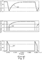
- Fig. 3 illustrates the typical current transitions in a chopper circuit, i.e. the freewheeling diode current 301, the IGBT current 302 and the resistor current 303.
- very small duty cycles are not desirable either because the turn-on times and the rise times are difficult to compensate for.
- Fig. 4 illustrates the temperature of an IGBT during typical operation thereof. As seen in Fig. 4 the IGBT temperature curve 401 reaches a temperature above 160 °C in less than 500 ms. Thus, the temperature increase of the IGBT is thus around 120 °C.
- new switching patterns are proposed in order to lower in particular the switching losses in applications where a plurality of chopper circuits are operated in parallel. More specifically, it is proposed to clamp the IGBT of at least one chopper circuit to be constantly either on or off for a certain time period, said certain time period being significantly longer than the switching period.
- the IGBT of the remaining chopper circuit or circuits may be operated with a given duty cycle which may be either lowered or increased in order to give the same equivalent duty cycle and thereby the same overall power dissipation compared to the scenario where none of the IGBTs is/are clamped. After the certain period, the IGBT of one or more other chopper circuits may be clamped.
- FIG. 5a An example involving two chopper circuits and thereby two IGBTs is depicted in Fig. 5a , where the upper graph shows the gate signal, T1, applied to the first IGBT, while the lower graph shows the gate signal, T2, applied to the second IGBT.
- the first IGBT is clamped to 1 during the clamping time period 501, while the second IGBT is operated with a certain switching period and a certain duty cycle.
- the switching pattern is reversed in that the second IGBT is clamped to 1 during the clamping time period 502, while the first IGBT is operated with a certain switching period and a certain duty cycle.
- Fig. 5a An example involving two chopper circuits and thereby two IGBTs is depicted in Fig. 5a , where the upper graph shows the gate signal, T1, applied to the first IGBT, while the lower graph shows the gate signal, T2, applied to the second IGBT.
- the first IGBT is clamped to 1 during
- the applied switching period is significantly shorter than the respective time periods 501, 502.
- the switching pattern is also altered at 350 ms, 450 ms and 500 ms.
- the clamping time periods 501, 502 depicted in Fig. 5a are around 50 ms.
- the switching period is around 2 ms and the duty cycle is around 66%, cf. Fig. 5b .
- the switching period 503, 504 is around 2 ms and the duty cycle is around 66%. It should be noted that both the clamping time periods 501, 502 and the switching periods 503, 504 could deviate from these values. Also, the clamping time period 501, 502 may not necessarily have the same length. The duty cycle may obviously vary over time and may thus differ from 66%.
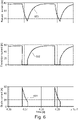
- Fig. 6 illustrates the current transitions in the chopper circuit when the new switching pattern is applied, i.e. the freewheeling diode current 601, the IGBT current 602 and the resistor current 603.
- an IGBT could be clamped to zero instead of being operated with a very low duty cycle while the duty cycle of another IGBT is increased in order to compensate for the clamped (to zero) IGBT.
- the clamping time period of an IGBT can be adjusted to be below the thermal time constant of the semi-conductor module to which the IGBT is thermally connected to ensure a smooth and controllable temperature profile over time.
- the appearances of temperature peaks and high temperature gradients are significantly reduced.
- the IGBT having the highest temperature could be clamped for a period being longer compared to other IGBTs.
- a more generic scheme could involve that clamping of IGBTs is only applied for very low and/or very high duty cycles. This would also imply that in case a duty cycle changes very rapidly, the state of a clamped IGBT should be changed accordingly and preferably immediately.
- Fig. 8 depicts one possible time-based control approach where a plurality of IGBTs (IGBT 1 - IGBT N ) are clamped in accordance with a predefined time table.
- IGBT 1 is clamped until a predefined time, t 1 , at which time the IGBT 1 is unclamped and IGBT 2 is clamped instead.
- IGBT 2 remains clamped until a predefined time, t 2 , at which time IGBT 2 is unclamped and IGBT N is clamped instead.
- This sequence of clamping/unclamping of IGBTs continuous as long as it is required.
- IGBT 1 may remain clamped until IGBT 2 reaches a predefined temperature, T 2 , at which temperature IGBT 2 is clamped and IGBT 1 is unclamped.
- T 2 a predefined temperature
- IGBT 1 a predefined temperature
- IGBT 1 is clamped and IGBT 2 is unclamped.
- Additional IGBTs may be involved in the temperature-based sequence of clamping/unclamping.
Landscapes
- Engineering & Computer Science (AREA)
- Power Engineering (AREA)
- Dc-Dc Converters (AREA)
- Life Sciences & Earth Sciences (AREA)
- Sustainable Development (AREA)
- Sustainable Energy (AREA)
- Chemical & Material Sciences (AREA)
- Combustion & Propulsion (AREA)
- Mechanical Engineering (AREA)
- General Engineering & Computer Science (AREA)
- Control Of Eletrric Generators (AREA)
Description
- The present invention relates to a method for increasing the power dissipation capability of a DC-chopper of a wind turbine power converter. The present invention relates in particular to a method for lowering the switching losses of the controllable switches of a plurality of chopper circuits forming the DC-chopper. The present invention further relates to a DC-chopper being operated in accordance with the method of the present invention.
- In the event of failures on power transmission or distribution grids, where the grid voltage drops to voltage levels which may be only a fraction of the nominal operating voltage, the power transfer from for example wind turbine generators to the power grid cannot be maintained. Furthermore, in order to support the power grid when the grid voltage recovers, wind turbine generators are expected to ramp up the active power very fast.
- One theoretical solution to the above requirement could be to pitch wind turbine generators out and in very fast during low-voltage ride through (LVRT) events. However, in order to avoid mechanical stress and in order to be able to recover power production immediately after voltage recovery, matching the power input and the power output by dissipating the deficit is the preferred solution from a practical point of view. The power dissipation is provided using a dump load resistor connected to a DC-link of a power converter. The amount of power to be dissipated is controlled through a chopper transistor. Depending on the required dump load capacity a plurality of chopper circuits each comprising a dump load resistor and a transistor may be connected in parallel. The transistor may be an insulated-gate bipolar transistor (IGBT), an integrated gate-commutated thyristor (IGCT), a gate turn-off thyristor (GTO) or another relevant power semiconductor switch. In following the term IGBT will be used as the general term for a transistor.
- The typical way of controlling the chopper IGBTs would be to measure the DC-link voltage and compare the measured voltage with a reference voltage. An error (error signal) between reference voltage and the measured voltage (the DC-link voltage or the square of the DC-link voltage) may be used to adjust the duty cycle (turn-on time) of the chopper IGBTs. The error signal could be fed through any type of controller, e.g. a proportional controller (P) and/or a proportional-integral controller (PI), which would then adjust the duty cycle in order to stabilize the DC-link voltage at (or close to) its reference value.
- The operation of chopper IGBTs is associated with power losses which consist of conducting losses and switching losses (turn-on loss and turn-off loss). Typically, the distribution of conducting losses and switching losses would be around 50%-50% depending on the chosen switching frequency.
- As it will be demonstrated in relation to
Fig. 4 conducting losses and in particular switching losses heat up an IGBT during operation. This heating may be the limiting factor in terms of the amount of power, and thereby energy, that can be dissipated in a chopper circuit. In fact, the temperature of an IGBT may increase up to 160-170 °C using conventional switching patterns. As a result, the power dissipation capability of a chopper circuit is significantly reduced. - It may be seen as an object of embodiments of the present invention to increase the power dissipation capability of a DC-chopper of a power converter.
- It may be seen as a further object of embodiments of the present invention to increase the power dissipation capability of a DC-chopper of a power converter by lowering the switching losses of a plurality of controllable switches.
- The principle underlying the present invention is applicable in all chopper applications having a plurality of chopper circuits arranged in parallel.
- Prior art
US2014/0070751 discloses s motor control apparatus includes a rectifier for rectifying AC power to output DC power; an inverter for performing power interconversion of DC power of a DC link and AC power being driving power or regenerative power of a motor by being connected to the DC link being a DC output side of the rectifier; and at least two resistance discharge units each for performing resistance discharge of DC power ofthe DC link, the resistance discharge units each being connected to the DC link, in which each resistance discharge unit starts a resistance discharge operation for performing resistance discharge of DC power of the DC link at a DC voltage value in the DC link exceeding a first threshold value and stops the resistance discharge operation at a DC voltage value in the DC link smaller than a second threshold value below the first threshold value. - Prior art
WO2017/108046 discloses a power dissipation system for a power converter of a wind turbine generator. The power dissipation system comprises at least a first dissipation module and a second dissipation module, each of the dissipation modules including a switch unit coupled to a respective dissipating element, a controller configured to provide a respective switch control signal to each of the switch units, and wherein the switch control signal of the first switch unit is different to the switch control signal of the second switch unit. The switch control signals may be phase shifted with respect to one another which reduces voltage fluctuations on the DC- link and achieves lower switching losses. - The above-mentioned objects are complied with by providing, in a first aspect, a method for simultaneous operation of a plurality of chopper circuits of a wind turbine power converter, in accordance with claim 1.
- In the present invention the first switching pattern involves that the controllable switching member of the first chopper circuit is clamped during the first time period. Clamping of the controllable switching member of the first chopper circuit involves that this controllable switching member is constantly on during the first time period.
- Clamping a controllable switching member is generally advantageous in that in particular the switching losses of the clamped switching member decreases significantly as long as the switching member is clamped, i.e. during the first time period.
- While the first switching pattern involves clamping of the controllable switching member of the first chopper circuit, the second switching pattern involves that a modulation pattern having a given switching frequency is applied to the controllable switching member of the second chopper circuit during the first time period.
- Generally, the first time period may be significantly longer than the switching period of the switching frequency applied to the controllable switching member of the second chopper circuit. Thus, the switching frequency applied to the controllable switching member of the second chopper circuit may have a switching period being at least 10 times shorter than the first time period, such as 15 times shorter than the first time period, such as 20 times shorter than the first time period.
- After the first time period the scenario is reversed so that during a second time period immediately following the first time period, the second switching pattern involves that the controllable switching member of the second chopper circuit is clamped. Again, clamping of the controllable switching member of the second chopper circuit involves that this controllable switching member is constantly on during the second time period. In this way the switching losses associated with the controllable switching member of the second chopper circuit may be reduced.
- While the second switching pattern involves clamping of the controllable switching member of the second chopper circuit, the first switching pattern involves that a modulation pattern having a given switching frequency is applied to the controllable switching member of the first chopper circuit during the second time period. Similar to the situation during the first time period the switching frequency applied to the controllable switching member of the first chopper circuit may have a switching period being at least 10 times shorter than the second time period, such as 15 times shorter than the second time period, such as 20 times shorter than the second time period.
- To summarize the above the controllable switching member of the first chopper circuit is clamped during the first time period, whereas the controllable switching member of the second chopper circuit is clamped during the second time period. As addressed above clamping of a controllable switching member reduces the switching losses of the switching member being clamped.
- It should be noted that the method according to the present invention is also applicable to arrangements having additional controllable switching members of additional chopper circuits, such as third, fourth, fifth, sixth and even more chopper circuits. The first, second and additional chopper circuits may be coupled in parallel. It should also be noted that more than one switching member may be clamped at the same time. Returning to the situation involving a first and a second chopper circuit the second time period may be triggered in response to a measured temperature of the controllable switching member of the second chopper circuit. Thus, while the controllable switching member of the first chopper circuit may be clamped in order to reduce switching losses, the temperature of the controllable switching member of the second chopper circuit is monitored. Then the temperature has reached a predefined value, the second time period may be initiated and as a consequence controllable switching member of the second chopper circuit may be clamped.
- In a second aspect, the present invention relates to a power dissipation chopper assembly for a wind turbine power converter, in accordance with claim 6.
- The above-mentioned definitions of for example switching patterns also apply in relation to the second aspect. It should also be noted that additional controllable switching members of additional chopper circuits, such as third, fourth, fifth, sixth and even more chopper circuits, may be provided. The first, second and additional chopper circuits may be coupled in parallel.
- The first switching pattern involves that the controllable switching member of the first chopper circuit is constantly on during the first time period. The second switching pattern involves that a modulation pattern having a given switching frequency is applied to the controllable switching member of the second chopper circuit during the first time period. The first time period may be significantly longer than the switching period of the switching frequency applied to the controllable switching member of the second chopper circuit. Thus, the switching frequency applied to the controllable switching member of the second chopper circuit may have a switching period being at least 10 times shorter than the first time period, such as 15 times shorter than the first time period, such as 20 times shorter than the first time period.
- The second switching pattern involves that the controllable switching member of the second chopper circuit is constantly on during a second time period that immediately follows the first time period. During this second time period the first switching pattern involves that a modulation pattern having a given switching frequency is applied to the controllable switching member of the first chopper circuit. Again, the second time period may be significantly longer than the switching period of the switching frequency applied to the controllable switching member of the first chopper circuit. Thus, the switching frequency applied to the controllable switching member of the first chopper circuit may have a switching period being at least 10 times shorter than the second time period, such as 15 times shorter than the second time period, such as 20 times shorter than the second time period. The second time period is triggered in response to a measured temperature of the controllable switching member of the second chopper circuit.
- In a third aspect the present invention relates to a wind turbine power converter comprising a power dissipation chopper assembly according to the second aspect, said chopper assembly being connected to a DC-link between a rectifier and an inverter of the wind turbine power converter.
- The present invention will now be described in further details with reference to the accompanying figures, wherein
-
Fig. 1 shows a DFIG wind turbine generator, -
Fig. 2 shows a converter branch and a converter DC-link including a plurality of parallel coupled chopper circuits, -
Fig. 3 shows diode, transistor and resistor currents of a typical prior art system, -
Fig. 4 show the transistor temperature of a typical prior art system, -
Fig. 5 shows the switching patterns of the present invention, -
Fig. 6 shows diode, transistor and resistor currents of a system using the switching patterns of the present invention, -
Fig. 7 show the transistor temperature of a system using the switching patterns of the present invention, and -
Fig. 8 shows a possible control strategy of the present invention. - While the invention is susceptible to various modifications and alternative forms specific embodiments have been shown by way of examples in the drawings and will be described in details herein. It should be understood, however, that the invention is not intended to be limited to the particular forms disclosed. Rather, the invention is to cover all modifications, equivalents, and alternatives falling within the scope of the invention as defined by the appended claims.
- In its broadest aspect the present invention relates to a method for increasing the power dissipation capability of a DC-chopper of a power converter by lowering the switching losses of a plurality of controllable switches of a plurality of chopper circuits. The controllable switches would normally be transistors, such as IGBTs. The method according to the present invention finds its primary use in relation to power converters, such as power converters used in relation to wind power plants or wind turbine generators.
-
Fig. 1 illustrates a variable speedwind turbine generator 100 comprising a doubly fed induction generator (DFIG) 101 and a power/frequency converter 102 connected to the rotor of thegenerator 101. Thegenerator 101 comprises a stator 103 connected to theutility grid 104 throughdisconnection switches 105 and the three-phase transformer 106. Thegenerator 101 may supply active stator power, Pst, reactive stator power, Qst, directly to theutility grid 104, or alternative receive power from theutility grid 104. The rotor of thegenerator 101 is mechanically driven by a wind turbine rotor (not shown) through a low speed shaft, gearing means and s high speed shaft (not shown). Furthermore, the rotor is electrically connected to the power/frequency converter 102. The power/frequency converter 102 may convert a variable AC voltage to an intermediate DC voltage and subsequently to a fixed AC voltage having a fixed frequency. - The power/
frequency converter 102 includes a rotor-side converter circuit 107 to rectify the AC voltage of thegenerator 101 to a DC voltage at the DC-link 108 or to invert the DC voltage to an AC voltage to be supplied to the rotor of thegenerator 101. The DC-link 108 smoothen the DC voltage over a DC-link capacitor 110. The grid-side converter circuit 109 inverts the DC voltage to an AC voltage with a preferred frequency or vice versa. - The active rotor power, PR, and reactive rotor power, QR, are coupled to or from the
utility grid 104 via thetransformer 106 and the disconnection switches 111. Thus, wind turbine generator may be controlled to supply electric power from the generator to the utility grid with a constant voltage and frequency regardless of changing wind and wind turbine rotor speeds. - The DC-link 108 further comprises at least two
chopper circuits chopper circuit link capacitor 110 and comprises at least a resistor and a controllable power switch connected in series. Moreover, each chopper circuit also comprises an anti-parallel diode for the resistor and an anti-parallel diode for the controllable power switch. The controllable power switch may be turned on and off in order to direct a current through the resistor and hereby dissipating power in the resistor. The DC-link voltage UDC may be lowered as charges are removed from the DC-link capacitor 110 by directing current through a resistor of one of the chopper circuits. Consequently, power generated by thegenerator 101 may be dissipated by activating one ormore chopper circuits utility grid 104. - The disconnection switches 105, 111 of the stator and the rotor facilitate that the
generator 101 may be disconnected from theutility grid 104 in connection with for example maintenance work on the wind turbine generator or an islanding situation in theutility grid 104. Furthermore, the wind turbine generator may be disconnected theutility grid 104 if a grid failure involving a significant voltage drop persists over a longer time period. - Although the above description relates to a DFIG configuration it should be noted that the present invention is also applicable to other wind turbine generator configurations, such as for example full scale configurations where all the generated power is delivered to the utility grid through a power converter connected to the stator of the generator.
-
Fig. 2 shows a branch/phase of the rotor-side converter 201 and the DC-link 202. The branch corresponds to one of the phases in a three-phase Pulse Width Modulation (PWM) frequency converter and includes two power switches, such asIGBTs anti-parallel diodes link capacitor 207 and the twochopper circuits Fig. 2 schematically illustrates how power may be dissipated in the resistors of thechopper circuits chopper circuits - As addressed above operating the controllable switch, such as an IGBT, of a chopper circuit of the type shown in
Figs. 1 and2 is associated with a power loss which consists of conducting losses and switching losses (turn-on loss and turn-off loss). Typical distribution of conducting losses and switching losses is around 50%-50% depending on the chosen switching frequency. The switching losses may in particular play a crucial role as the turn-on losses depend on the current flowing due to the inductive part of the chopper resistor. When turning off the IGBT, the current through the transistor drops to zero, but due to the inductive part of the chopper resistor, the current through the resistor cannot abruptly go to zero. Instead it commutates to the freewheeling diode and decline according to the time constant of the R/L circuit. - For high chopper loads, the duty cycle applied to the IGBT is close to 1 which means that the IGBT turn on immediately after turn-off. In this case the chopper resistor current may typically not have reached zero, and hence the transistor turns on with a freewheeling diode current still flowing which thereby commutates to the IGBT. This is associated with turn-on switching losses.
Fig. 3 illustrates the typical current transitions in a chopper circuit, i.e. the freewheeling diode current 301, the IGBT current 302 and theresistor current 303. Moreover, in order provide an accurate control very small duty cycles are not desirable either because the turn-on times and the rise times are difficult to compensate for. - The conducting losses and switching losses heat up the IGBT during operation. This heating may be the limiting factor in terms of the amount of power, and thereby energy, what can be dissipated in a chopper circuit.
Fig. 4 illustrates the temperature of an IGBT during typical operation thereof. As seen inFig. 4 theIGBT temperature curve 401 reaches a temperature above 160 °C in less than 500 ms. Thus, the temperature increase of the IGBT is thus around 120 °C. - According to the present invention new switching patterns are proposed in order to lower in particular the switching losses in applications where a plurality of chopper circuits are operated in parallel. More specifically, it is proposed to clamp the IGBT of at least one chopper circuit to be constantly either on or off for a certain time period, said certain time period being significantly longer than the switching period. The IGBT of the remaining chopper circuit or circuits may be operated with a given duty cycle which may be either lowered or increased in order to give the same equivalent duty cycle and thereby the same overall power dissipation compared to the scenario where none of the IGBTs is/are clamped. After the certain period, the IGBT of one or more other chopper circuits may be clamped.
- An example involving two chopper circuits and thereby two IGBTs is depicted in
Fig. 5a , where the upper graph shows the gate signal, T1, applied to the first IGBT, while the lower graph shows the gate signal, T2, applied to the second IGBT. As seenFig. 1 the first IGBT is clamped to 1 during theclamping time period 501, while the second IGBT is operated with a certain switching period and a certain duty cycle. When the time reaches 400 ms the switching pattern is reversed in that the second IGBT is clamped to 1 during theclamping time period 502, while the first IGBT is operated with a certain switching period and a certain duty cycle. As depicted inFig. 5 the applied switching period is significantly shorter than therespective time periods clamping time periods Fig. 5a are around 50 ms. The switching period is around 2 ms and the duty cycle is around 66%, cf.Fig. 5b . -
Fig. 5b is a close-up ofFig. 5a around T=0.35 s where the upper graph shows the gate signal, T1, applied to the first IGBT, while the lower graph shows the gate signal, T2, applied to the second IGBT. The dashedline 505 at T=0.35 is the point in time where the second IGBT becomes unclamped and the first IGBT becomes clamped. As addressed above theswitching period clamping time periods periods clamping time period - The lack of switching of one IGBT around half of the time reduces the IGBT-related losses with around 25% assuming the before-mentioned 50%-50% split between conduction losses and switching losses. Moreover, since the duty cycle of the IBGT being switched is reduced, the duration between turn-off and turn-on is increased compared to a traditional switching strategy. As a result, the inductive current running in the diode in the off time will have more time to decline whereby the current level in the diode at turn-on is lower. This lower current level in the diode at turn-on further reduces the switching losses.
-
Fig. 6 illustrates the current transitions in the chopper circuit when the new switching pattern is applied, i.e. the freewheeling diode current 601, the IGBT current 602 and theresistor current 603. - Applying the new switching pattern in the same chopper circuits and under the same conditions as describe in relation to
Figs. 3 and4 the temperature of the IGBT will be as shown inFig. 7 . Compared toFig. 4 the temperature increase of the IGBT has been lowered from around 120 °C to 85 °C as a result of the new switching pattern. - The underlying principle of the present invention may be applied in various scenarios. As an example an IGBT could be clamped to zero instead of being operated with a very low duty cycle while the duty cycle of another IGBT is increased in order to compensate for the clamped (to zero) IGBT.
- Even further, the clamping time period of an IGBT can be adjusted to be below the thermal time constant of the semi-conductor module to which the IGBT is thermally connected to ensure a smooth and controllable temperature profile over time. Thus, with this approach the appearances of temperature peaks and high temperature gradients are significantly reduced. In relation to temperature the IGBT having the highest temperature could be clamped for a period being longer compared to other IGBTs.
- A more generic scheme could involve that clamping of IGBTs is only applied for very low and/or very high duty cycles. This would also imply that in case a duty cycle changes very rapidly, the state of a clamped IGBT should be changed accordingly and preferably immediately.
-
Fig. 8 depicts one possible time-based control approach where a plurality of IGBTs (IGBT1 - IGBTN) are clamped in accordance with a predefined time table. Thus, according to the control approach depicted inFig. 8 IGBT1 is clamped until a predefined time, t1, at which time the IGBT1 is unclamped and IGBT2 is clamped instead. IGBT2 remains clamped until a predefined time, t2, at which time IGBT2 is unclamped and IGBTN is clamped instead. This sequence of clamping/unclamping of IGBTs continuous as long as it is required. As addressed above the sequence of clamping/unclamping of IGBTs could also rely on measured IGBT temperatures in that IGBT1 may remain clamped until IGBT2 reaches a predefined temperature, T2, at which temperature IGBT2 is clamped and IGBT1 is unclamped. When IGBT1 reaches a predefined temperature, T1, IGBT1 is clamped and IGBT2 is unclamped. Additional IGBTs may be involved in the temperature-based sequence of clamping/unclamping.
Claims (8)
- A method for simultaneous operation of a plurality of chopper circuits of a wind turbine power converter, wherein each chopper circuit comprises a power dissipation member, the method comprising the steps of- operating a controllable switching member of a first chopper circuit in accordance with a first switching pattern, and- operating a controllable switching member of a second chopper circuit in accordance with a second switching pattern,wherein the first switching pattern is different from the second switching pattern during a first time period (501), and wherein the first switching pattern involves that the controllable switching member of the first chopper circuit is clamped during the first time period, wherein clamping of the controllable switching member of the first chopper circuit involves that this controllable switching member is constantly on during the first time period,wherein the second switching pattern involves that a modulation pattern having a given switching frequency is applied to the controllable switching member of the second chopper circuit during the first time period (501), andwherein the first switching pattern involves that a modulation pattern having a given switching frequency is applied to the controllable switching member of the first chopper circuit during a second time period (502) immediately following the first time period (501),wherein the second switching pattern involves that the controllable switching member of the second chopper circuit is clamped during the second time period (502), andwherein clamping of the controllable switching member of the second chopper circuit involves that this controllable switching member is constantly on during the second time period.
- A method according to claim 1, wherein the switching frequency applied to the controllable switching member of the second chopper circuit has a switching period being at least 10 times shorter than the first time period, such as 15 times shorter than the first time period, such as 20 times shorter than the first time period.
- A method according to claim 1, wherein the switching frequency applied to the controllable switching member of the first chopper circuit has a switching period being at least 10 times shorter than the second time period, such as 15 times shorter than the second time period, such as 20 times shorter than the second time period.
- A method according to any of claims 1-3, wherein the second time period is triggered in response to a measured temperature of the controllable switching member of the second chopper circuit.
- A method according to any of the preceding claims, wherein additional chopper circuits are provided, and wherein the first, second and additional chopper circuits are coupled in parallel.
- A power dissipation chopper assembly for a wind turbine power converter, the power dissipation chopper assembly comprising- a first chopper circuit (112) comprising a power dissipation member and controllable switching member configured to be operated in accordance with a first switching pattern,- a second chopper circuit (113) comprising a power dissipation member and controllable switching member configured to be operated in accordance with a second switching pattern, and- a control unit configured for simultaneous operation of the controllable switching members in accordance with the first and second switching patterns, wherein the first switching pattern is different from the second switching pattern during a first time period (501), and wherein the first switching pattern involves that the controllable switching member of the first chopper circuit is clamped during the first time period,- wherein clamping the controllable switching member of the first chopper circuit involves that the controllable switching member of the first chopper circuit is constantly on during the first time period (501), and wherein the second switching pattern involves that a modulation pattern having a given switching frequency is applied to the controllable switching member of the second chopper circuit during the first time period (501), and- wherein, during a second time period (502) immediately following the first time period (501), the second switching pattern involves that the controllable switching member of the second chopper circuit is constantly on during the second time period (502), and wherein the first switching pattern involves that a modulation pattern having a given switching frequency is applied to the controllable switching member of the first chopper circuit during the second time period (502), and wherein the second time period (502) is triggered in response to a measured temperature of the controllable switching member of the second chopper circuit.
- A power dissipation chopper assembly according to claim 6, wherein additional chopper circuits are provided, and wherein the first, second and additional chopper circuits are coupled in parallel.
- A wind turbine power converter comprising a power dissipation chopper assembly according to any of claims 6-7, said chopper assembly being connected to a DC-link between a rectifier and an inverter of the wind turbine power converter.
Applications Claiming Priority (2)
| Application Number | Priority Date | Filing Date | Title |
|---|---|---|---|
| DKPA201770960 | 2017-12-19 | ||
| PCT/DK2018/050316 WO2019120402A1 (en) | 2017-12-19 | 2018-11-30 | A method for operating a plurality of chopper circuits |
Publications (2)
| Publication Number | Publication Date |
|---|---|
| EP3729629A1 EP3729629A1 (en) | 2020-10-28 |
| EP3729629B1 true EP3729629B1 (en) | 2022-10-19 |
Family
ID=66993144
Family Applications (1)
| Application Number | Title | Priority Date | Filing Date |
|---|---|---|---|
| EP18815512.1A Active EP3729629B1 (en) | 2017-12-19 | 2018-11-30 | A method for operating a plurality of chopper circuits |
Country Status (5)
| Country | Link |
|---|---|
| US (1) | US11258345B2 (en) |
| EP (1) | EP3729629B1 (en) |
| CN (1) | CN111466073B (en) |
| ES (1) | ES2928907T3 (en) |
| WO (1) | WO2019120402A1 (en) |
Families Citing this family (5)
| Publication number | Priority date | Publication date | Assignee | Title |
|---|---|---|---|---|
| ES3048485T3 (en) * | 2019-08-13 | 2025-12-10 | Vestas Wind Sys As | Intelligent discharge control for modular multilevel converter |
| EP3780366A1 (en) * | 2019-08-13 | 2021-02-17 | Vestas Wind Systems A/S | Dc chopper for mmc cell with integrated chopper resistor |
| CN114725974A (en) * | 2021-01-06 | 2022-07-08 | 许继集团有限公司 | Energy consumption valve bank branch time-sharing input device and method |
| US12107507B2 (en) * | 2021-09-02 | 2024-10-01 | Rivian Ip Holdings, Llc | Dual active bridge converter control with switching loss distribution |
| US12407253B2 (en) * | 2021-12-17 | 2025-09-02 | Rivian Ip Holdings, Llc | Dual active bridge converter control with select inactive states for loss distribution |
Family Cites Families (20)
| Publication number | Priority date | Publication date | Assignee | Title |
|---|---|---|---|---|
| GB2118742B (en) | 1982-04-20 | 1985-06-05 | Northern Eng Ind | Electrical generator control system |
| US7385372B2 (en) | 2004-05-27 | 2008-06-10 | Siemens Energy & Automation, Inc. | Auxiliary bus system |
| JP2008526179A (en) | 2004-12-28 | 2008-07-17 | ヴェスタス,ウィンド,システムズ エー/エス | Control method for wind turbines connected to the electricity distribution network |
| JP2009027886A (en) * | 2007-07-23 | 2009-02-05 | Sanken Electric Co Ltd | Ac-dc converter |
| CN100561839C (en) * | 2007-10-11 | 2009-11-18 | 天津大学 | Wind power generation power conversion device of direct-driving type permanent magnet synchronous motor |
| US8198742B2 (en) * | 2007-12-28 | 2012-06-12 | Vestas Wind Systems A/S | Variable speed wind turbine with a doubly-fed induction generator and rotor and grid inverters that use scalar controls |
| JP4911733B2 (en) * | 2009-03-13 | 2012-04-04 | オムロン株式会社 | Power converter, power conditioner, and power generation system |
| US8400085B2 (en) * | 2009-09-04 | 2013-03-19 | Rockwell Automation Technologies, Inc. | Dynamic braking for current source converter based drive |
| CN101697458A (en) * | 2009-10-26 | 2010-04-21 | 株洲南车时代电气股份有限公司 | Three-phase auxiliary inverter |
| CN102226638A (en) * | 2011-03-30 | 2011-10-26 | 合肥市顺昌不锈钢设备制造有限公司 | Induction-type tank welding seam drying and heating device |
| CN102185329A (en) * | 2011-05-04 | 2011-09-14 | 华北电力大学 | Super-capacitor-based DC voltage sag suppression device and suppression method thereof |
| EP2621070A1 (en) | 2012-01-26 | 2013-07-31 | Siemens Aktiengesellschaft | Method and arrangement for operating a wind turbine converter |
| JP5670398B2 (en) * | 2012-09-10 | 2015-02-18 | ファナック株式会社 | Motor control device having at least two resistance discharge means |
| WO2015097815A1 (en) * | 2013-12-26 | 2015-07-02 | 三菱電機株式会社 | Power conversion device |
| CN104917199B (en) * | 2014-03-14 | 2019-11-19 | 长沙理工大学 | Grid-connected flexible series-parallel multifunctional energy controller for AC/DC microgrid |
| CN105391081A (en) * | 2014-09-09 | 2016-03-09 | 艾默生网络能源有限公司 | DC bus chopper circuit, control method and device therefor, and wind power system |
| CN104836257A (en) * | 2015-06-02 | 2015-08-12 | 中国农业大学 | Integrated low-voltage ride through regulation and control device of wind power generation |
| WO2017108046A1 (en) * | 2015-12-22 | 2017-06-29 | Vestas Wind Systems A/S | Power dissipation system and control method for a wind turbine power converter |
| CN105835703B (en) * | 2016-03-29 | 2018-10-23 | 中车永济电机有限公司 | A kind of subway traction convertor main circuit |
| US10103663B1 (en) * | 2017-04-18 | 2018-10-16 | General Electric Company | Control method for protecting switching devices in power converters in doubly fed induction generator power systems |
-
2018
- 2018-11-30 ES ES18815512T patent/ES2928907T3/en active Active
- 2018-11-30 CN CN201880079956.1A patent/CN111466073B/en active Active
- 2018-11-30 EP EP18815512.1A patent/EP3729629B1/en active Active
- 2018-11-30 US US16/956,462 patent/US11258345B2/en active Active
- 2018-11-30 WO PCT/DK2018/050316 patent/WO2019120402A1/en not_active Ceased
Also Published As
| Publication number | Publication date |
|---|---|
| US11258345B2 (en) | 2022-02-22 |
| CN111466073A (en) | 2020-07-28 |
| US20200362823A1 (en) | 2020-11-19 |
| CN111466073B (en) | 2023-08-15 |
| WO2019120402A1 (en) | 2019-06-27 |
| EP3729629A1 (en) | 2020-10-28 |
| ES2928907T3 (en) | 2022-11-23 |
Similar Documents
| Publication | Publication Date | Title |
|---|---|---|
| EP3729629B1 (en) | A method for operating a plurality of chopper circuits | |
| US10367407B2 (en) | Method and device for controlling a voltage-controlled power semiconductor switch that can be switched off again | |
| CN104011987B (en) | Systems and methods for low speed control of polyphase AC motors | |
| Ma et al. | Thermal optimised modulation methods of three-level neutral-point-clamped inverter for 10 MW wind turbines under low-voltage ride through | |
| US9479075B2 (en) | Multilevel converter system | |
| EP3657661A1 (en) | Conversion circuit, control method, and power supply device | |
| US7928592B2 (en) | Wind turbine with parallel converters utilizing a plurality of isolated generator windings | |
| US9252681B2 (en) | Power converter with a first string having controllable semiconductor switches and a second string having switching modules | |
| US8923016B2 (en) | Solar module for generating a D.C. voltage and method for its operation | |
| US20170310234A1 (en) | Power converter topology for use in an energy storage system | |
| CA2655023C (en) | Load power supply device comprising integrated energy storage | |
| US9325273B2 (en) | Method and system for driving electric machines | |
| Hristov | An Application of Three-Phase PWM AC-DC-AC Rectifiter | |
| EP3487066B1 (en) | System and method for operating a doubly fed induction generator system to reduce harmonics | |
| EP2783108B1 (en) | Wind power station | |
| Junchen et al. | Variable frequency AC input BLDC low loss control technology for aviation pump | |
| Kaur et al. | Switching loss reduction for efficacy of interleaved parallel inverters fed induction motor drives | |
| Chattopadhyay et al. | Non-isolated high-frequency-link to feed auxiliary bridges of asymmetrical cascaded multilevel inverter | |
| AU2012358950B9 (en) | System and method for low speed control of polyphase AC machine | |
| Ouni et al. | A variable switching frequency control method for active front end multilevel rectifier | |
| Li et al. | High power snubberless IGBT converter for direct-drive wind power generation system | |
| Soni et al. | A Current Source Inverter with Advanced External Circuit and Control Method | |
| KR20170112059A (en) | Apparatus and method for controlling switching module | |
| HK1197114B (en) | System and method for low speed control of polyphase ac machine |
Legal Events
| Date | Code | Title | Description |
|---|---|---|---|
| STAA | Information on the status of an ep patent application or granted ep patent |
Free format text: STATUS: UNKNOWN |
|
| STAA | Information on the status of an ep patent application or granted ep patent |
Free format text: STATUS: THE INTERNATIONAL PUBLICATION HAS BEEN MADE |
|
| PUAI | Public reference made under article 153(3) epc to a published international application that has entered the european phase |
Free format text: ORIGINAL CODE: 0009012 |
|
| STAA | Information on the status of an ep patent application or granted ep patent |
Free format text: STATUS: REQUEST FOR EXAMINATION WAS MADE |
|
| 17P | Request for examination filed |
Effective date: 20200616 |
|
| AK | Designated contracting states |
Kind code of ref document: A1 Designated state(s): AL AT BE BG CH CY CZ DE DK EE ES FI FR GB GR HR HU IE IS IT LI LT LU LV MC MK MT NL NO PL PT RO RS SE SI SK SM TR |
|
| AX | Request for extension of the european patent |
Extension state: BA ME |
|
| DAV | Request for validation of the european patent (deleted) | ||
| DAX | Request for extension of the european patent (deleted) | ||
| STAA | Information on the status of an ep patent application or granted ep patent |
Free format text: STATUS: EXAMINATION IS IN PROGRESS |
|
| 17Q | First examination report despatched |
Effective date: 20210409 |
|
| RIC1 | Information provided on ipc code assigned before grant |
Ipc: H02P 3/22 20060101ALI20220420BHEP Ipc: H02J 3/38 20060101ALI20220420BHEP Ipc: H02M 1/32 20070101ALI20220420BHEP Ipc: H02M 5/44 20060101AFI20220420BHEP |
|
| GRAP | Despatch of communication of intention to grant a patent |
Free format text: ORIGINAL CODE: EPIDOSNIGR1 |
|
| STAA | Information on the status of an ep patent application or granted ep patent |
Free format text: STATUS: GRANT OF PATENT IS INTENDED |
|
| INTG | Intention to grant announced |
Effective date: 20220602 |
|
| GRAS | Grant fee paid |
Free format text: ORIGINAL CODE: EPIDOSNIGR3 |
|
| GRAA | (expected) grant |
Free format text: ORIGINAL CODE: 0009210 |
|
| STAA | Information on the status of an ep patent application or granted ep patent |
Free format text: STATUS: THE PATENT HAS BEEN GRANTED |
|
| AK | Designated contracting states |
Kind code of ref document: B1 Designated state(s): AL AT BE BG CH CY CZ DE DK EE ES FI FR GB GR HR HU IE IS IT LI LT LU LV MC MK MT NL NO PL PT RO RS SE SI SK SM TR |
|
| REG | Reference to a national code |
Ref country code: GB Ref legal event code: FG4D |
|
| REG | Reference to a national code |
Ref country code: CH Ref legal event code: EP |
|
| REG | Reference to a national code |
Ref country code: DE Ref legal event code: R096 Ref document number: 602018042039 Country of ref document: DE |
|
| REG | Reference to a national code |
Ref country code: IE Ref legal event code: FG4D |
|
| REG | Reference to a national code |
Ref country code: AT Ref legal event code: REF Ref document number: 1526198 Country of ref document: AT Kind code of ref document: T Effective date: 20221115 |
|
| REG | Reference to a national code |
Ref country code: ES Ref legal event code: FG2A Ref document number: 2928907 Country of ref document: ES Kind code of ref document: T3 Effective date: 20221123 |
|
| REG | Reference to a national code |
Ref country code: LT Ref legal event code: MG9D |
|
| REG | Reference to a national code |
Ref country code: NL Ref legal event code: MP Effective date: 20221019 |
|
| REG | Reference to a national code |
Ref country code: AT Ref legal event code: MK05 Ref document number: 1526198 Country of ref document: AT Kind code of ref document: T Effective date: 20221019 |
|
| PG25 | Lapsed in a contracting state [announced via postgrant information from national office to epo] |
Ref country code: NL Free format text: LAPSE BECAUSE OF FAILURE TO SUBMIT A TRANSLATION OF THE DESCRIPTION OR TO PAY THE FEE WITHIN THE PRESCRIBED TIME-LIMIT Effective date: 20221019 |
|
| PG25 | Lapsed in a contracting state [announced via postgrant information from national office to epo] |
Ref country code: SE Free format text: LAPSE BECAUSE OF FAILURE TO SUBMIT A TRANSLATION OF THE DESCRIPTION OR TO PAY THE FEE WITHIN THE PRESCRIBED TIME-LIMIT Effective date: 20221019 Ref country code: PT Free format text: LAPSE BECAUSE OF FAILURE TO SUBMIT A TRANSLATION OF THE DESCRIPTION OR TO PAY THE FEE WITHIN THE PRESCRIBED TIME-LIMIT Effective date: 20230220 Ref country code: NO Free format text: LAPSE BECAUSE OF FAILURE TO SUBMIT A TRANSLATION OF THE DESCRIPTION OR TO PAY THE FEE WITHIN THE PRESCRIBED TIME-LIMIT Effective date: 20230119 Ref country code: LT Free format text: LAPSE BECAUSE OF FAILURE TO SUBMIT A TRANSLATION OF THE DESCRIPTION OR TO PAY THE FEE WITHIN THE PRESCRIBED TIME-LIMIT Effective date: 20221019 Ref country code: FI Free format text: LAPSE BECAUSE OF FAILURE TO SUBMIT A TRANSLATION OF THE DESCRIPTION OR TO PAY THE FEE WITHIN THE PRESCRIBED TIME-LIMIT Effective date: 20221019 Ref country code: AT Free format text: LAPSE BECAUSE OF FAILURE TO SUBMIT A TRANSLATION OF THE DESCRIPTION OR TO PAY THE FEE WITHIN THE PRESCRIBED TIME-LIMIT Effective date: 20221019 |
|
| PG25 | Lapsed in a contracting state [announced via postgrant information from national office to epo] |
Ref country code: RS Free format text: LAPSE BECAUSE OF FAILURE TO SUBMIT A TRANSLATION OF THE DESCRIPTION OR TO PAY THE FEE WITHIN THE PRESCRIBED TIME-LIMIT Effective date: 20221019 Ref country code: PL Free format text: LAPSE BECAUSE OF FAILURE TO SUBMIT A TRANSLATION OF THE DESCRIPTION OR TO PAY THE FEE WITHIN THE PRESCRIBED TIME-LIMIT Effective date: 20221019 Ref country code: LV Free format text: LAPSE BECAUSE OF FAILURE TO SUBMIT A TRANSLATION OF THE DESCRIPTION OR TO PAY THE FEE WITHIN THE PRESCRIBED TIME-LIMIT Effective date: 20221019 Ref country code: IS Free format text: LAPSE BECAUSE OF FAILURE TO SUBMIT A TRANSLATION OF THE DESCRIPTION OR TO PAY THE FEE WITHIN THE PRESCRIBED TIME-LIMIT Effective date: 20230219 Ref country code: HR Free format text: LAPSE BECAUSE OF FAILURE TO SUBMIT A TRANSLATION OF THE DESCRIPTION OR TO PAY THE FEE WITHIN THE PRESCRIBED TIME-LIMIT Effective date: 20221019 Ref country code: GR Free format text: LAPSE BECAUSE OF FAILURE TO SUBMIT A TRANSLATION OF THE DESCRIPTION OR TO PAY THE FEE WITHIN THE PRESCRIBED TIME-LIMIT Effective date: 20230120 |
|
| P01 | Opt-out of the competence of the unified patent court (upc) registered |
Effective date: 20230521 |
|
| REG | Reference to a national code |
Ref country code: CH Ref legal event code: PL |
|
| REG | Reference to a national code |
Ref country code: DE Ref legal event code: R097 Ref document number: 602018042039 Country of ref document: DE |
|
| REG | Reference to a national code |
Ref country code: BE Ref legal event code: MM Effective date: 20221130 |
|
| PG25 | Lapsed in a contracting state [announced via postgrant information from national office to epo] |
Ref country code: SM Free format text: LAPSE BECAUSE OF FAILURE TO SUBMIT A TRANSLATION OF THE DESCRIPTION OR TO PAY THE FEE WITHIN THE PRESCRIBED TIME-LIMIT Effective date: 20221019 Ref country code: RO Free format text: LAPSE BECAUSE OF FAILURE TO SUBMIT A TRANSLATION OF THE DESCRIPTION OR TO PAY THE FEE WITHIN THE PRESCRIBED TIME-LIMIT Effective date: 20221019 Ref country code: MC Free format text: LAPSE BECAUSE OF FAILURE TO SUBMIT A TRANSLATION OF THE DESCRIPTION OR TO PAY THE FEE WITHIN THE PRESCRIBED TIME-LIMIT Effective date: 20221019 Ref country code: LI Free format text: LAPSE BECAUSE OF NON-PAYMENT OF DUE FEES Effective date: 20221130 Ref country code: EE Free format text: LAPSE BECAUSE OF FAILURE TO SUBMIT A TRANSLATION OF THE DESCRIPTION OR TO PAY THE FEE WITHIN THE PRESCRIBED TIME-LIMIT Effective date: 20221019 Ref country code: DK Free format text: LAPSE BECAUSE OF FAILURE TO SUBMIT A TRANSLATION OF THE DESCRIPTION OR TO PAY THE FEE WITHIN THE PRESCRIBED TIME-LIMIT Effective date: 20221019 Ref country code: CZ Free format text: LAPSE BECAUSE OF FAILURE TO SUBMIT A TRANSLATION OF THE DESCRIPTION OR TO PAY THE FEE WITHIN THE PRESCRIBED TIME-LIMIT Effective date: 20221019 Ref country code: CH Free format text: LAPSE BECAUSE OF NON-PAYMENT OF DUE FEES Effective date: 20221130 |
|
| PLBE | No opposition filed within time limit |
Free format text: ORIGINAL CODE: 0009261 |
|
| STAA | Information on the status of an ep patent application or granted ep patent |
Free format text: STATUS: NO OPPOSITION FILED WITHIN TIME LIMIT |
|
| PG25 | Lapsed in a contracting state [announced via postgrant information from national office to epo] |
Ref country code: SK Free format text: LAPSE BECAUSE OF FAILURE TO SUBMIT A TRANSLATION OF THE DESCRIPTION OR TO PAY THE FEE WITHIN THE PRESCRIBED TIME-LIMIT Effective date: 20221019 Ref country code: LU Free format text: LAPSE BECAUSE OF NON-PAYMENT OF DUE FEES Effective date: 20221130 Ref country code: AL Free format text: LAPSE BECAUSE OF FAILURE TO SUBMIT A TRANSLATION OF THE DESCRIPTION OR TO PAY THE FEE WITHIN THE PRESCRIBED TIME-LIMIT Effective date: 20221019 |
|
| 26N | No opposition filed |
Effective date: 20230720 |
|
| PG25 | Lapsed in a contracting state [announced via postgrant information from national office to epo] |
Ref country code: IE Free format text: LAPSE BECAUSE OF NON-PAYMENT OF DUE FEES Effective date: 20221130 |
|
| PG25 | Lapsed in a contracting state [announced via postgrant information from national office to epo] |
Ref country code: SI Free format text: LAPSE BECAUSE OF FAILURE TO SUBMIT A TRANSLATION OF THE DESCRIPTION OR TO PAY THE FEE WITHIN THE PRESCRIBED TIME-LIMIT Effective date: 20221019 Ref country code: BE Free format text: LAPSE BECAUSE OF NON-PAYMENT OF DUE FEES Effective date: 20221130 |
|
| PG25 | Lapsed in a contracting state [announced via postgrant information from national office to epo] |
Ref country code: CY Free format text: LAPSE BECAUSE OF FAILURE TO SUBMIT A TRANSLATION OF THE DESCRIPTION OR TO PAY THE FEE WITHIN THE PRESCRIBED TIME-LIMIT Effective date: 20221019 |
|
| PG25 | Lapsed in a contracting state [announced via postgrant information from national office to epo] |
Ref country code: MK Free format text: LAPSE BECAUSE OF FAILURE TO SUBMIT A TRANSLATION OF THE DESCRIPTION OR TO PAY THE FEE WITHIN THE PRESCRIBED TIME-LIMIT Effective date: 20221019 Ref country code: IT Free format text: LAPSE BECAUSE OF FAILURE TO SUBMIT A TRANSLATION OF THE DESCRIPTION OR TO PAY THE FEE WITHIN THE PRESCRIBED TIME-LIMIT Effective date: 20221019 Ref country code: HU Free format text: LAPSE BECAUSE OF FAILURE TO SUBMIT A TRANSLATION OF THE DESCRIPTION OR TO PAY THE FEE WITHIN THE PRESCRIBED TIME-LIMIT; INVALID AB INITIO Effective date: 20181130 |
|
| PG25 | Lapsed in a contracting state [announced via postgrant information from national office to epo] |
Ref country code: TR Free format text: LAPSE BECAUSE OF FAILURE TO SUBMIT A TRANSLATION OF THE DESCRIPTION OR TO PAY THE FEE WITHIN THE PRESCRIBED TIME-LIMIT Effective date: 20221019 |
|
| PG25 | Lapsed in a contracting state [announced via postgrant information from national office to epo] |
Ref country code: BG Free format text: LAPSE BECAUSE OF FAILURE TO SUBMIT A TRANSLATION OF THE DESCRIPTION OR TO PAY THE FEE WITHIN THE PRESCRIBED TIME-LIMIT Effective date: 20221019 |
|
| PG25 | Lapsed in a contracting state [announced via postgrant information from national office to epo] |
Ref country code: MT Free format text: LAPSE BECAUSE OF FAILURE TO SUBMIT A TRANSLATION OF THE DESCRIPTION OR TO PAY THE FEE WITHIN THE PRESCRIBED TIME-LIMIT Effective date: 20221019 |
|
| PGFP | Annual fee paid to national office [announced via postgrant information from national office to epo] |
Ref country code: DE Payment date: 20251126 Year of fee payment: 8 |
|
| PGFP | Annual fee paid to national office [announced via postgrant information from national office to epo] |
Ref country code: GB Payment date: 20251125 Year of fee payment: 8 |
|
| PGFP | Annual fee paid to national office [announced via postgrant information from national office to epo] |
Ref country code: FR Payment date: 20251124 Year of fee payment: 8 |
|
| PGFP | Annual fee paid to national office [announced via postgrant information from national office to epo] |
Ref country code: ES Payment date: 20251209 Year of fee payment: 8 |