EP3726674A1 - Semiconductor laser - Google Patents
Semiconductor laser Download PDFInfo
- Publication number
- EP3726674A1 EP3726674A1 EP18888008.2A EP18888008A EP3726674A1 EP 3726674 A1 EP3726674 A1 EP 3726674A1 EP 18888008 A EP18888008 A EP 18888008A EP 3726674 A1 EP3726674 A1 EP 3726674A1
- Authority
- EP
- European Patent Office
- Prior art keywords
- layer
- semiconductor laser
- temperature
- temperature control
- flat layer
- Prior art date
- Legal status (The legal status is an assumption and is not a legal conclusion. Google has not performed a legal analysis and makes no representation as to the accuracy of the status listed.)
- Granted
Links
Images



Classifications
-
- H—ELECTRICITY
- H01—ELECTRIC ELEMENTS
- H01S—DEVICES USING THE PROCESS OF LIGHT AMPLIFICATION BY STIMULATED EMISSION OF RADIATION [LASER] TO AMPLIFY OR GENERATE LIGHT; DEVICES USING STIMULATED EMISSION OF ELECTROMAGNETIC RADIATION IN WAVE RANGES OTHER THAN OPTICAL
- H01S5/00—Semiconductor lasers
- H01S5/02—Structural details or components not essential to laser action
- H01S5/026—Monolithically integrated components, e.g. waveguides, monitoring photo-detectors, drivers
- H01S5/0261—Non-optical elements, e.g. laser driver components, heaters
-
- H—ELECTRICITY
- H01—ELECTRIC ELEMENTS
- H01S—DEVICES USING THE PROCESS OF LIGHT AMPLIFICATION BY STIMULATED EMISSION OF RADIATION [LASER] TO AMPLIFY OR GENERATE LIGHT; DEVICES USING STIMULATED EMISSION OF ELECTROMAGNETIC RADIATION IN WAVE RANGES OTHER THAN OPTICAL
- H01S5/00—Semiconductor lasers
- H01S5/06—Arrangements for controlling the laser output parameters, e.g. by operating on the active medium
- H01S5/0607—Arrangements for controlling the laser output parameters, e.g. by operating on the active medium by varying physical parameters other than the potential of the electrodes, e.g. by an electric or magnetic field, mechanical deformation, pressure, light, temperature
- H01S5/0612—Arrangements for controlling the laser output parameters, e.g. by operating on the active medium by varying physical parameters other than the potential of the electrodes, e.g. by an electric or magnetic field, mechanical deformation, pressure, light, temperature controlled by temperature
-
- H—ELECTRICITY
- H01—ELECTRIC ELEMENTS
- H01S—DEVICES USING THE PROCESS OF LIGHT AMPLIFICATION BY STIMULATED EMISSION OF RADIATION [LASER] TO AMPLIFY OR GENERATE LIGHT; DEVICES USING STIMULATED EMISSION OF ELECTROMAGNETIC RADIATION IN WAVE RANGES OTHER THAN OPTICAL
- H01S5/00—Semiconductor lasers
- H01S5/06—Arrangements for controlling the laser output parameters, e.g. by operating on the active medium
- H01S5/062—Arrangements for controlling the laser output parameters, e.g. by operating on the active medium by varying the potential of the electrodes
- H01S5/0625—Arrangements for controlling the laser output parameters, e.g. by operating on the active medium by varying the potential of the electrodes in multi-section lasers
- H01S5/06255—Controlling the frequency of the radiation
- H01S5/06258—Controlling the frequency of the radiation with DFB-structure
-
- H—ELECTRICITY
- H01—ELECTRIC ELEMENTS
- H01S—DEVICES USING THE PROCESS OF LIGHT AMPLIFICATION BY STIMULATED EMISSION OF RADIATION [LASER] TO AMPLIFY OR GENERATE LIGHT; DEVICES USING STIMULATED EMISSION OF ELECTROMAGNETIC RADIATION IN WAVE RANGES OTHER THAN OPTICAL
- H01S5/00—Semiconductor lasers
- H01S5/10—Construction or shape of the optical resonator, e.g. extended or external cavity, coupled cavities, bent-guide, varying width, thickness or composition of the active region
- H01S5/12—Construction or shape of the optical resonator, e.g. extended or external cavity, coupled cavities, bent-guide, varying width, thickness or composition of the active region the resonator having a periodic structure, e.g. in distributed feedback [DFB] lasers
-
- H—ELECTRICITY
- H01—ELECTRIC ELEMENTS
- H01S—DEVICES USING THE PROCESS OF LIGHT AMPLIFICATION BY STIMULATED EMISSION OF RADIATION [LASER] TO AMPLIFY OR GENERATE LIGHT; DEVICES USING STIMULATED EMISSION OF ELECTROMAGNETIC RADIATION IN WAVE RANGES OTHER THAN OPTICAL
- H01S5/00—Semiconductor lasers
- H01S5/10—Construction or shape of the optical resonator, e.g. extended or external cavity, coupled cavities, bent-guide, varying width, thickness or composition of the active region
- H01S5/12—Construction or shape of the optical resonator, e.g. extended or external cavity, coupled cavities, bent-guide, varying width, thickness or composition of the active region the resonator having a periodic structure, e.g. in distributed feedback [DFB] lasers
- H01S5/1203—Construction or shape of the optical resonator, e.g. extended or external cavity, coupled cavities, bent-guide, varying width, thickness or composition of the active region the resonator having a periodic structure, e.g. in distributed feedback [DFB] lasers over only a part of the length of the active region
-
- H—ELECTRICITY
- H01—ELECTRIC ELEMENTS
- H01S—DEVICES USING THE PROCESS OF LIGHT AMPLIFICATION BY STIMULATED EMISSION OF RADIATION [LASER] TO AMPLIFY OR GENERATE LIGHT; DEVICES USING STIMULATED EMISSION OF ELECTROMAGNETIC RADIATION IN WAVE RANGES OTHER THAN OPTICAL
- H01S5/00—Semiconductor lasers
- H01S5/30—Structure or shape of the active region; Materials used for the active region
- H01S5/34—Structure or shape of the active region; Materials used for the active region comprising quantum well or superlattice structures, e.g. single quantum well [SQW] lasers, multiple quantum well [MQW] lasers or graded index separate confinement heterostructure [GRINSCH] lasers
- H01S5/3401—Structure or shape of the active region; Materials used for the active region comprising quantum well or superlattice structures, e.g. single quantum well [SQW] lasers, multiple quantum well [MQW] lasers or graded index separate confinement heterostructure [GRINSCH] lasers having no PN junction, e.g. unipolar lasers, intersubband lasers, quantum cascade lasers
- H01S5/3402—Structure or shape of the active region; Materials used for the active region comprising quantum well or superlattice structures, e.g. single quantum well [SQW] lasers, multiple quantum well [MQW] lasers or graded index separate confinement heterostructure [GRINSCH] lasers having no PN junction, e.g. unipolar lasers, intersubband lasers, quantum cascade lasers intersubband lasers, e.g. transitions within the conduction or valence bands
-
- H—ELECTRICITY
- H01—ELECTRIC ELEMENTS
- H01S—DEVICES USING THE PROCESS OF LIGHT AMPLIFICATION BY STIMULATED EMISSION OF RADIATION [LASER] TO AMPLIFY OR GENERATE LIGHT; DEVICES USING STIMULATED EMISSION OF ELECTROMAGNETIC RADIATION IN WAVE RANGES OTHER THAN OPTICAL
- H01S5/00—Semiconductor lasers
- H01S5/02—Structural details or components not essential to laser action
- H01S5/028—Coatings ; Treatment of the laser facets, e.g. etching, passivation layers or reflecting layers
- H01S5/0287—Facet reflectivity
-
- H—ELECTRICITY
- H01—ELECTRIC ELEMENTS
- H01S—DEVICES USING THE PROCESS OF LIGHT AMPLIFICATION BY STIMULATED EMISSION OF RADIATION [LASER] TO AMPLIFY OR GENERATE LIGHT; DEVICES USING STIMULATED EMISSION OF ELECTROMAGNETIC RADIATION IN WAVE RANGES OTHER THAN OPTICAL
- H01S5/00—Semiconductor lasers
- H01S5/06—Arrangements for controlling the laser output parameters, e.g. by operating on the active medium
- H01S5/062—Arrangements for controlling the laser output parameters, e.g. by operating on the active medium by varying the potential of the electrodes
- H01S5/06233—Controlling other output parameters than intensity or frequency
- H01S5/06246—Controlling other output parameters than intensity or frequency controlling the phase
-
- H—ELECTRICITY
- H01—ELECTRIC ELEMENTS
- H01S—DEVICES USING THE PROCESS OF LIGHT AMPLIFICATION BY STIMULATED EMISSION OF RADIATION [LASER] TO AMPLIFY OR GENERATE LIGHT; DEVICES USING STIMULATED EMISSION OF ELECTROMAGNETIC RADIATION IN WAVE RANGES OTHER THAN OPTICAL
- H01S5/00—Semiconductor lasers
- H01S5/06—Arrangements for controlling the laser output parameters, e.g. by operating on the active medium
- H01S5/068—Stabilisation of laser output parameters
- H01S5/06804—Stabilisation of laser output parameters by monitoring an external parameter, e.g. temperature
-
- H—ELECTRICITY
- H01—ELECTRIC ELEMENTS
- H01S—DEVICES USING THE PROCESS OF LIGHT AMPLIFICATION BY STIMULATED EMISSION OF RADIATION [LASER] TO AMPLIFY OR GENERATE LIGHT; DEVICES USING STIMULATED EMISSION OF ELECTROMAGNETIC RADIATION IN WAVE RANGES OTHER THAN OPTICAL
- H01S5/00—Semiconductor lasers
- H01S5/06—Arrangements for controlling the laser output parameters, e.g. by operating on the active medium
- H01S5/068—Stabilisation of laser output parameters
- H01S5/0683—Stabilisation of laser output parameters by monitoring the optical output parameters
- H01S5/06837—Stabilising otherwise than by an applied electric field or current, e.g. by controlling the temperature
-
- H—ELECTRICITY
- H01—ELECTRIC ELEMENTS
- H01S—DEVICES USING THE PROCESS OF LIGHT AMPLIFICATION BY STIMULATED EMISSION OF RADIATION [LASER] TO AMPLIFY OR GENERATE LIGHT; DEVICES USING STIMULATED EMISSION OF ELECTROMAGNETIC RADIATION IN WAVE RANGES OTHER THAN OPTICAL
- H01S5/00—Semiconductor lasers
- H01S5/06—Arrangements for controlling the laser output parameters, e.g. by operating on the active medium
- H01S5/068—Stabilisation of laser output parameters
- H01S5/0683—Stabilisation of laser output parameters by monitoring the optical output parameters
- H01S5/0687—Stabilising the frequency of the laser
-
- H—ELECTRICITY
- H01—ELECTRIC ELEMENTS
- H01S—DEVICES USING THE PROCESS OF LIGHT AMPLIFICATION BY STIMULATED EMISSION OF RADIATION [LASER] TO AMPLIFY OR GENERATE LIGHT; DEVICES USING STIMULATED EMISSION OF ELECTROMAGNETIC RADIATION IN WAVE RANGES OTHER THAN OPTICAL
- H01S5/00—Semiconductor lasers
- H01S5/20—Structure or shape of the semiconductor body to guide the optical wave ; Confining structures perpendicular to the optical axis, e.g. index or gain guiding, stripe geometry, broad area lasers, gain tailoring, transverse or lateral reflectors, special cladding structures, MQW barrier reflection layers
- H01S5/22—Structure or shape of the semiconductor body to guide the optical wave ; Confining structures perpendicular to the optical axis, e.g. index or gain guiding, stripe geometry, broad area lasers, gain tailoring, transverse or lateral reflectors, special cladding structures, MQW barrier reflection layers having a ridge or stripe structure
- H01S5/2205—Structure or shape of the semiconductor body to guide the optical wave ; Confining structures perpendicular to the optical axis, e.g. index or gain guiding, stripe geometry, broad area lasers, gain tailoring, transverse or lateral reflectors, special cladding structures, MQW barrier reflection layers having a ridge or stripe structure comprising special burying or current confinement layers
Definitions
- the present invention relates to a semiconductor laser used for, for example, exhaust gas component analysis or the like, and in particular, to a quantum cascade laser or the like.
- QCL quantum cascade laser
- a sharp resonance phenomenon occurs by positionally accurately forming the reflective end surface of a diffraction grating so as to obtain a predetermined light phase ( ⁇ /4); however, the reflective end surface is formed by cleavage, and therefore a phase shift as illustrated in Fig. 6 is likely to occur to cause a wavelength jump. For this reason, there is also a problem that a non-defective yield is very low (e.g., around approximately 30 %).
- the present invention has been made in order to solve the problems described above, and a main intended object thereof is to make it possible to tune a wavelength while suppressing a variation in the intensity of laser light in a semiconductor laser such as a QCL.
- an intended object is also an improvement in non-defective yield, or the like.
- the semiconductor laser according to the present invention is one including: a core layer having an active layer and a diffraction grating layer optically coupled to the active layer; and paired clad layers arranged sandwiching the core layer, and formed with a waveguide along the core layer.
- the semiconductor laser includes: a flat layer provided continuously with the diffraction grating layer along the waveguide; and a temperature control mechanism for controlling the temperature of the flat layer to a temperature different from the diffraction grating layer.
- Such a configuration makes it possible to, while suppressing a variation in the intensity of laser light outputted by injecting a constant current into the active layer, tune a laser oscillation wavelength by controlling the temperature of the flat layer to thereby change the refractive index of it.
- tune a laser oscillation wavelength by controlling the temperature of the flat layer to thereby change the refractive index of it.
- one end and the other end of the waveguide are respectively provided with a reflective surface and a light lead-out surface, and an end surface of the flat layer serves as the reflective surface.
- the adjustment of the refractive index of the flat layer by the temperature control makes it possible to adjust the phase of light reflected at the reflective surface ex post facto so as to be shifted to, for example, ⁇ /4, and therefore non-defective products in which a wavelength jump hardly occurs can be manufactured in a high yield.
- the temperature control mechanism includes a temperature control electrode provided in a site corresponding to the flat layer and the temperature of the flat layer can be controlled by applying current to the flat layer via the temperature control electrode can be cited.
- the active layer is formed of a multiple quantum well structure in which multiple well layers are connected in a multistep manner, and light is generated by an optical transition between subbands formed in the quantum wells.
- the multiple well layers may be ones having different thicknesses.
- a drive controller that controls driving of the semiconductor laser, one including: a temperature control part that controls the temperature control mechanism to control the temperature of the flat layer; and a laser drive part that injects current into the core layer to generate laser oscillation can be cited.
- an oscillation wavelength can be tuned while suppressing a variation in the intensity of laser light, for example, in the case of use for the component analysis of exhaust gas or the like, it is possible to improve the accuracy of the analysis.
- the flat layer is provided continuously with a terminal of the diffraction grating layer, for example, a phase shift at the reflective surface due to cleavage can be cancelled by the temperature control, and therefore defective products conventionally produced due to the phase shift can be suppressed from being produced, making it possible to dramatically improve a non-defective yield.
- a laser device 100 in this embodiment is one provided with a semiconductor laser 1 and a drive controller 2 that controls driving of the semiconductor laser 1.
- This semiconductor laser 1 is a distributed feedback quantum well cascade laser (hereinafter also referred to as a QCL), and as illustrated in Fig. 1 and Fig. 2 , for example, one in which on a substrate 3 made of n-InP, a buffer layer 4 and a core layer 5 made of InP, an upper clad layer 6 made of InP, and a cap layer 7 made of InGaAs are stacked in this order by crystal growth based on an MOCVD method, an MBE method, or the like.
- the buffer layer 4 and/or the substrate 3 function as a lower clad layer.
- a lower electrode T2 and an upper electrode T1 are respectively provided, and by applying voltage between these electrodes T1 and T2 to inject current having a threshold value or more into the core layer 5, the core layer 5 emits light and the semiconductor laser 1 generates laser oscillation.
- the core layer 5 consists of: an active layer 51; and guide layers 52 and 53 provided above and below the active layer 51, and is one of a unipolar type in which semiconductor layers of the same type (n-type or p-type) are stacked.
- the active layer 51 is one structured to connect multiple well layers having different thicknesses in a multistep manner, and in this embodiment, adapted to emit light having a mid-infrared or longer wavelength by the optical transitions between levels (subbands) present in the conduction band.
- the active layer 51 is configured by alternately stacking a semiconductor layer serving as a light emitting region and a semiconductor layer serving as an injection region by a predetermined number.
- the semiconductor layer serving as a light emitting region is configured by alternately stacking InGaAs and InAlAs and the semiconductor layer serving as an injection region is configured by alternately stacking InGaAs and InAlAs.
- the guide layers 52 and 53 are ones made of InGaAs, and carry a function as a waveguide for propagating the light generated in the active layer 52.
- a diffraction grating layer 8 in which diffraction grating s 8a are arrayed with a constant period ⁇ is formed by microgrooving the upper surface of the upper guide layer 52 of these guide layers 52 and 53 to form a one-dimensional stripe structure.
- the diffraction grating layer 8 is optically coupled to the active layer 52, and the light generated in the active layer 52 travels in a direction (hereinafter also referred to as a waveguide direction) orthogonal to a groove direction while reflecting by the respective diffraction grating s 8a.
- a direction hereinafter also referred to as a waveguide direction
- only light having a constant wavelength determined by the period ⁇ of the diffraction gratings 8a is constantly acted on by the diffraction gratings 8a to remain long in the active layer 52, and is amplified to thereby generate the laser oscillation.
- one end surface of the core layer 5 (the terminal surface in the waveguide direction) is a reflective surface 5a formed by cleavage, and the other end surface is subjected to non-reflection treatment to serve as a light lead-out surface 5b from which the laser light is led out.
- a flat layer 9 is formed continuously with the diffraction grating layer 8 in the core layer 5.
- the flat layer 9 is one formed by not microgrooving a certain area of the upper guide layer 52 on the reflective surface 5a side, and accordingly, one end surface of the flat layer 9 is continuous with the diffraction grating layer 8, whereas the other end surface serves as the reflective surface 5a.
- the flat layer 9 can also be said to be a part of the diffraction grating layer 8 and a part whose diffraction grating period is different from the other part.
- a temperature control mechanism S for independently controlling the temperature of the flat layer 9 to a temperature different from that of the diffraction grating layer 8 is provided.
- the temperature control mechanism S in this embodiment is one including a temperature control electrode S1 provided above the flat layer 9.
- the temperature control electrode S1 is one provided above the flat layer and on the upper surface of the cap layer 7, and disposed separated from the upper electrode T1 in the waveguide direction in an electrically unconnected state.
- the flat layer 9 is configured so that the temperature thereof can be controlled by applying voltage to the temperature control electrode S1 to apply current to the flat layer 9 and thereby generating resistance heat.
- the resulting temperature change changes the refractive index of the flat layer 9; however, in the semiconductor laser 100 of this embodiment, the core layer 5 is one of a unipolar type as described above, and therefore the influence of the voltage on the refractive index of the flat layer 9 (the influence of the quantum confined Stark effect on the refractive index) does not occur.
- the drive controller 2 is one consisting of: a digital electric circuit including a CPU, a memory, an I/O port, and the like; an analog electric circuit including an amplifier, a buffer, and the like; and an A/D converter, a D/A converter, and the like interposed between them, and the CPU and its peripheral devices cooperate in accordance with a predetermined program stored in the memory, thereby functioning as an operation mode setting part 21 that sets the operation mode of the semiconductor laser 1, a laser drive part 22 that supplies laser drive current I 1 to the upper electrode T1 to generate the light in the active layer 51, and a temperature control part 23 that supplies temperature control current I 2 to the temperature control electrode S1 to control the temperature of the flat layer 9 as illustrated in Fig. 1 .
- the operation mode setting part 21 receives it, and in accordance with the selected operation mode, the laser drive part 22 and the temperature control part 23 operate.
- a first operation mode of the two types of operation modes is a mode that controls the temperature of the flat layer 9 to thereby change the refractive index thereof, and fixedly controls a phase at the end surface of the flat layer 9 to ⁇ /4 to generate laser oscillation at a Bragg wavelength determined by the optical path length of the diffraction gratings 8a.
- the temperature control part 23 applies voltage to the temperature control electrode of the QCL to apply the temperature control current I 2 toward the lower electrode T2.
- the value of the temperature control current I 2 may be larger or smaller than threshold current I th for laser oscillation.
- the resulting resistance heat changes the temperature of the flat layer 9 located between the temperature control electrode S1 and the lower electrode T2, and the refractive index is changed.
- the current causing the phase at the end surface of the flat layer 9 to be ⁇ /4 is preliminarily measured, and as illustrated in Fig. 3 , the temperature control part 23 applies the voltage causing the current to the temperature control electrode S1.
- the laser drive part 22 applies the voltage to the upper electrode T1 with the phase at the end surface of the flat layer 9 controlled to ⁇ /4 by the temperature control part 23, and injects the laser drive current, which is equal to or more than the threshold value I th and constant, into the active layer 51.
- the laser drive current which is equal to or more than the threshold value I th and constant, into the active layer 51.
- Fig. 3 an example of pulse oscillation is illustrated, but continuous oscillation is also possible.
- a second operation mode is a mode that adjusts the wavelength of the laser light to a desired value while preventing a variation in the intensity of the laser light as much as possible.
- the laser drive part 22 first applies the voltage to the upper electrode T1 to continuously inject the constant laser drive current equal to or more than the threshold value I th into the active layer 51. In doing so, the laser light is continuously oscillated, and a variation in the intensity of it is suppressed.
- the temperature control part 23 changes the temperature control current I 2 with time as illustrated in Fig. 4 . This allows the temperature of the flat layer 9 to be changed with time, and correspondingly, the refractive index of the flat layer 9 is also temporally changed.
- the phase at the end surface of the flat layer 9 is temporally changed, and a laser oscillation wavelength is temporally changed, i.e., swept.
- the wavelength of the laser light is adapted to be swept within a stop bandwidth around ⁇ /4 by controlling the phase at the end surface of the flat layer 9.
- the laser drive part 22 may allow laser oscillation to be generated using repetitive pulses. This is pseudo continuous oscillation of laser light.
- the light phase at the reflective surface 5a is controlled to ⁇ /4 regardless of a shift in cleavage, the most effective feedback can be obtained to enable laser oscillation in a single wavelength mode without a wavelength jump.
- the oscillation wavelength of the laser light can be changed while continuing to prevent a variation in the intensity of the laser light as much as possible, for example, when quantifying concentration at respective wavelengths for gas analysis or the like, the intensity of the laser light is not significantly varies among the respective wavelengths, and therefore an S/N ratio can be stabilized to contribute to improving analysis accuracy.
- the flat layer 9 may be provided in the diffraction grating layer 8.
- the temperature control electrode S1 and the upper electrode T1 are provided above the flat layer 9 and above the diffraction grating layer 8 respectively separately.
- an oscillation wavelength can be controlled by changing the temperature of the flat layer 9 and therefore changing the refractive index thereof.
- the phase at the reflective surface 5a is controlled in a feedforward-like manner that applies a predetermined constant current to the temperature control electrode S1; however, for example, the temperature control part 23 may be adapted to perform the feedback control of current (or voltage) to be applied to the temperature control electrode S1 so that with an oscillation wavelength monitored, the oscillation wavelength becomes equal to a Bragg wavelength, or alternatively the temperature control part 23 may be adapted to perform the feedback control or the like of voltage (current) so that with a temperature sensor for directly or indirectly measuring the temperature of the flat layer 9 provided, the temperature by the temperature sensor becomes equal to a desired temperature.
- the temperature control mechanism is not one based on current but may be one using a Peltier element or a refrigerant.
- the present invention is applicable not only to a quantum cascade laser but also to another type of semiconductor laser as long as it has a DFB structure and also to a semiconductor laser having a DBR structure.
- an oscillation wavelength can be tuned while suppressing a variation in the intensity of laser light, for example, in the case of use for the component analysis of exhaust gas or the like, it is possible to improve the accuracy of the analysis.
Landscapes
- Physics & Mathematics (AREA)
- Condensed Matter Physics & Semiconductors (AREA)
- General Physics & Mathematics (AREA)
- Electromagnetism (AREA)
- Optics & Photonics (AREA)
- Semiconductor Lasers (AREA)
- Geometry (AREA)
Abstract
Description
- The present invention relates to a semiconductor laser used for, for example, exhaust gas component analysis or the like, and in particular, to a quantum cascade laser or the like.
- Recently, there has been proposed a quantum cascade laser (hereinafter also referred to as a QCL) that oscillates laser light in a mid-infrared range as a light source used for the component analysis of sample gas such as exhaust gas. This sort of QCL can output very sharp single wavelength laser light, and can therefore improve analysis accuracy.
- Meanwhile, analysis sometimes requires measurement using light beams having multiple wavelengths by wavelength sweeping or the like. Therefore, in conventional QCLs, a wavelength is tuned by changing injection current.
- However, in such a case, a large difference may occur between the intensity of laser light at some wavelength and the intensity of laser light at another wavelength, and for example, when quantifying concentration at such respective wavelengths, there may occur a problem of an unstable S/N ratio because of the difference in laser light intensity.
- Also, for example, in the case of a distributed feedback QCL having a DFB structure, a sharp resonance phenomenon occurs by positionally accurately forming the reflective end surface of a diffraction grating so as to obtain a predetermined light phase (λ/4); however, the reflective end surface is formed by cleavage, and therefore a phase shift as illustrated in
Fig. 6 is likely to occur to cause a wavelength jump. For this reason, there is also a problem that a non-defective yield is very low (e.g., around approximately 30 %). - Japanese Unexamined Patent Publication
JP-A2017-123445 - The present invention has been made in order to solve the problems described above, and a main intended object thereof is to make it possible to tune a wavelength while suppressing a variation in the intensity of laser light in a semiconductor laser such as a QCL. In addition, secondarily, an intended object is also an improvement in non-defective yield, or the like.
- That is, the semiconductor laser according to the present invention is one including: a core layer having an active layer and a diffraction grating layer optically coupled to the active layer; and paired clad layers arranged sandwiching the core layer, and formed with a waveguide along the core layer. Further, the semiconductor laser includes: a flat layer provided continuously with the diffraction grating layer along the waveguide; and a temperature control mechanism for controlling the temperature of the flat layer to a temperature different from the diffraction grating layer.
- Such a configuration makes it possible to, while suppressing a variation in the intensity of laser light outputted by injecting a constant current into the active layer, tune a laser oscillation wavelength by controlling the temperature of the flat layer to thereby change the refractive index of it. As a result, for example, when qualifying concentration at respective wavelengths for gas analysis or the like, the variation in the intensity of the laser light is suppressed, and therefore an S/N ratio can be stabilized to contribute to improving analysis accuracy.
- It is preferable that one end and the other end of the waveguide are respectively provided with a reflective surface and a light lead-out surface, and an end surface of the flat layer serves as the reflective surface.
- In such a configuration, even when the location of the reflective surface is displaced from a predetermined location by causes such as formation by cleavage, the adjustment of the refractive index of the flat layer by the temperature control makes it possible to adjust the phase of light reflected at the reflective surface ex post facto so as to be shifted to, for example, λ/4, and therefore non-defective products in which a wavelength jump hardly occurs can be manufactured in a high yield.
- As a specific embodiment of the temperature control mechanism, one configured so that the temperature control mechanism includes a temperature control electrode provided in a site corresponding to the flat layer and the temperature of the flat layer can be controlled by applying current to the flat layer via the temperature control electrode can be cited.
- It is preferable that the active layer is formed of a multiple quantum well structure in which multiple well layers are connected in a multistep manner, and light is generated by an optical transition between subbands formed in the quantum wells. In addition, the multiple well layers may be ones having different thicknesses.
- As a semiconductor laser making the effects of the present invention more remarkable, a quantum cascade laser can be cited.
- As a drive controller that controls driving of the semiconductor laser, one including: a temperature control part that controls the temperature control mechanism to control the temperature of the flat layer; and a laser drive part that injects current into the core layer to generate laser oscillation can be cited.
- According to the present invention configured as described, since an oscillation wavelength can be tuned while suppressing a variation in the intensity of laser light, for example, in the case of use for the component analysis of exhaust gas or the like, it is possible to improve the accuracy of the analysis.
- Also, in the semiconductor laser in which an end surface of the flat layer is made to serve as the reflective surface, i.e., the flat layer is provided continuously with a terminal of the diffraction grating layer, for example, a phase shift at the reflective surface due to cleavage can be cancelled by the temperature control, and therefore defective products conventionally produced due to the phase shift can be suppressed from being produced, making it possible to dramatically improve a non-defective yield.
-
- [
Fig. 1 ]
Fig. 1 is a schematic diagram illustrating the whole of a semiconductor laser device in one embodiment of the present invention. - [
Fig. 2 ]
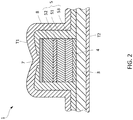
Fig. 2 is a cross-sectional view illustrating a semiconductor laser in the same embodiment. - [
Fig. 3 ]
Fig. 3 is a diagram for explaining a method for driving the semiconductor laser in the same embodiment. - [
Fig. 4 ]
Fig. 4 is a diagram for explaining a method for driving the semiconductor laser in the same embodiment. - [
Fig. 5 ]
Fig. 5 is a schematic diagram illustrating the whole of a semiconductor laser device in another embodiment of the present invention. - [
Fig. 6 ]
Fig. 6 is a diagram for explaining a wavelength jump that has occurred in a conventional distributed feedback QCL. -
- 100 Semiconductor laser device
- 1 Distributed feedback semiconductor laser
- 2 Drive controller
- 3, 4, 6 Clad layer
- 5 Core layer
- 51 Active layer
- 5a Reflective surface
- 5b Light lead-out surface
- 8 diffraction grating layer
- 9 Flat layer
- S Temperature control mechanism
- S1 Temperature control electrode
- In the following, one embodiment of a
laser device 100 according to the present invention will be described with reference to drawings. - As illustrated in
Fig. 1 , alaser device 100 in this embodiment is one provided with asemiconductor laser 1 and adrive controller 2 that controls driving of thesemiconductor laser 1. - First, the
semiconductor laser 1 will be described. - This
semiconductor laser 1 is a distributed feedback quantum well cascade laser (hereinafter also referred to as a QCL), and as illustrated inFig. 1 andFig. 2 , for example, one in which on asubstrate 3 made of n-InP, abuffer layer 4 and acore layer 5 made of InP, anupper clad layer 6 made of InP, and a cap layer 7 made of InGaAs are stacked in this order by crystal growth based on an MOCVD method, an MBE method, or the like. In addition, thebuffer layer 4 and/or thesubstrate 3 function as a lower clad layer. - Also, on the lower surface of the
substrate 3 and on the upper surface of the cap layer 7, a lower electrode T2 and an upper electrode T1 are respectively provided, and by applying voltage between these electrodes T1 and T2 to inject current having a threshold value or more into thecore layer 5, thecore layer 5 emits light and thesemiconductor laser 1 generates laser oscillation. - The
core layer 5 consists of: anactive layer 51; andguide layers active layer 51, and is one of a unipolar type in which semiconductor layers of the same type (n-type or p-type) are stacked. - The
active layer 51 is one structured to connect multiple well layers having different thicknesses in a multistep manner, and in this embodiment, adapted to emit light having a mid-infrared or longer wavelength by the optical transitions between levels (subbands) present in the conduction band. Describing more specifically, theactive layer 51 is configured by alternately stacking a semiconductor layer serving as a light emitting region and a semiconductor layer serving as an injection region by a predetermined number. In this embodiment, the semiconductor layer serving as a light emitting region is configured by alternately stacking InGaAs and InAlAs and the semiconductor layer serving as an injection region is configured by alternately stacking InGaAs and InAlAs. - The guide layers 52 and 53 are ones made of InGaAs, and carry a function as a waveguide for propagating the light generated in the
active layer 52. - Further, in this embodiment, a
diffraction grating layer 8 in which diffraction grating s 8a are arrayed with a constant period Λ is formed by microgrooving the upper surface of theupper guide layer 52 of these guide layers 52 and 53 to form a one-dimensional stripe structure. - The
diffraction grating layer 8 is optically coupled to theactive layer 52, and the light generated in theactive layer 52 travels in a direction (hereinafter also referred to as a waveguide direction) orthogonal to a groove direction while reflecting by the respective diffraction grating s 8a. At this time, only light having a constant wavelength determined by the period Λ of thediffraction gratings 8a is constantly acted on by thediffraction gratings 8a to remain long in theactive layer 52, and is amplified to thereby generate the laser oscillation. - In addition, in the
semiconductor laser 1, one end surface of the core layer 5 (the terminal surface in the waveguide direction) is areflective surface 5a formed by cleavage, and the other end surface is subjected to non-reflection treatment to serve as a light lead-outsurface 5b from which the laser light is led out. - Further, in this embodiment, a
flat layer 9 is formed continuously with thediffraction grating layer 8 in thecore layer 5. - The
flat layer 9 is one formed by not microgrooving a certain area of theupper guide layer 52 on thereflective surface 5a side, and accordingly, one end surface of theflat layer 9 is continuous with thediffraction grating layer 8, whereas the other end surface serves as thereflective surface 5a. In addition, when changing a point of view, theflat layer 9 can also be said to be a part of thediffraction grating layer 8 and a part whose diffraction grating period is different from the other part. - Further, in this embodiment, a temperature control mechanism S for independently controlling the temperature of the
flat layer 9 to a temperature different from that of thediffraction grating layer 8 is provided. The temperature control mechanism S in this embodiment is one including a temperature control electrode S1 provided above theflat layer 9. - The temperature control electrode S1 is one provided above the flat layer and on the upper surface of the cap layer 7, and disposed separated from the upper electrode T1 in the waveguide direction in an electrically unconnected state. Further, the
flat layer 9 is configured so that the temperature thereof can be controlled by applying voltage to the temperature control electrode S1 to apply current to theflat layer 9 and thereby generating resistance heat. In addition, the resulting temperature change changes the refractive index of theflat layer 9; however, in thesemiconductor laser 100 of this embodiment, thecore layer 5 is one of a unipolar type as described above, and therefore the influence of the voltage on the refractive index of the flat layer 9 (the influence of the quantum confined Stark effect on the refractive index) does not occur. - Next, the
drive controller 2 will be described. - Although not illustrated, the
drive controller 2 is one consisting of: a digital electric circuit including a CPU, a memory, an I/O port, and the like; an analog electric circuit including an amplifier, a buffer, and the like; and an A/D converter, a D/A converter, and the like interposed between them, and the CPU and its peripheral devices cooperate in accordance with a predetermined program stored in the memory, thereby functioning as an operationmode setting part 21 that sets the operation mode of thesemiconductor laser 1, alaser drive part 22 that supplies laser drive current I1 to the upper electrode T1 to generate the light in theactive layer 51, and atemperature control part 23 that supplies temperature control current I2 to the temperature control electrode S1 to control the temperature of theflat layer 9 as illustrated inFig. 1 . - Next, the operation of the
semiconductor laser device 100 configured as described will be described. - In this embodiment, roughly, two types of operation modes are prepared, and for example, when any of the operation modes is selected by a user's input, the operation
mode setting part 21 receives it, and in accordance with the selected operation mode, thelaser drive part 22 and thetemperature control part 23 operate. - A first operation mode of the two types of operation modes is a mode that controls the temperature of the
flat layer 9 to thereby change the refractive index thereof, and fixedly controls a phase at the end surface of theflat layer 9 to λ/4 to generate laser oscillation at a Bragg wavelength determined by the optical path length of thediffraction gratings 8a. - Describing more specifically, in the first operation mode, the
temperature control part 23 applies voltage to the temperature control electrode of the QCL to apply the temperature control current I2 toward the lower electrode T2. In addition, the value of the temperature control current I2 may be larger or smaller than threshold current Ith for laser oscillation. - In doing so, the resulting resistance heat changes the temperature of the
flat layer 9 located between the temperature control electrode S1 and the lower electrode T2, and the refractive index is changed. - In this embodiment, the current causing the phase at the end surface of the
flat layer 9 to be λ/4 is preliminarily measured, and as illustrated inFig. 3 , thetemperature control part 23 applies the voltage causing the current to the temperature control electrode S1. - Further, as described, the
laser drive part 22 applies the voltage to the upper electrode T1 with the phase at the end surface of theflat layer 9 controlled to λ/4 by thetemperature control part 23, and injects the laser drive current, which is equal to or more than the threshold value Ith and constant, into theactive layer 51. In addition, inFig. 3 , an example of pulse oscillation is illustrated, but continuous oscillation is also possible. - A second operation mode is a mode that adjusts the wavelength of the laser light to a desired value while preventing a variation in the intensity of the laser light as much as possible.
- In this second mode, the
laser drive part 22 first applies the voltage to the upper electrode T1 to continuously inject the constant laser drive current equal to or more than the threshold value Ith into theactive layer 51. In doing so, the laser light is continuously oscillated, and a variation in the intensity of it is suppressed. - In this state, by temporally changing the temperature of the
flat layer 9, the refractive index thereof is changed. - More specifically, the
temperature control part 23 changes the temperature control current I2 with time as illustrated inFig. 4 . This allows the temperature of theflat layer 9 to be changed with time, and correspondingly, the refractive index of theflat layer 9 is also temporally changed. - As a result, the phase at the end surface of the
flat layer 9 is temporally changed, and a laser oscillation wavelength is temporally changed, i.e., swept. Here, the wavelength of the laser light is adapted to be swept within a stop bandwidth around λ/4 by controlling the phase at the end surface of theflat layer 9. - In addition, as illustrated in the same diagram, the
laser drive part 22 may allow laser oscillation to be generated using repetitive pulses. This is pseudo continuous oscillation of laser light. - Further, according to the
semiconductor laser device 100 as described above, the following effects can be produced. - First, since a phase shift at the
reflective surface 5a due to cleavage can be cancelled by the temperature control, defective products in which a wavelength jump is caused by the phase shift can be suppressed from being produced, making it possible to dramatically improve a non-defective yield. - For example, since in the first operation mode, the light phase at the
reflective surface 5a is controlled to λ/4 regardless of a shift in cleavage, the most effective feedback can be obtained to enable laser oscillation in a single wavelength mode without a wavelength jump. - Also, since as in the second operation mode, the oscillation wavelength of the laser light can be changed while continuing to prevent a variation in the intensity of the laser light as much as possible, for example, when quantifying concentration at respective wavelengths for gas analysis or the like, the intensity of the laser light is not significantly varies among the respective wavelengths, and therefore an S/N ratio can be stabilized to contribute to improving analysis accuracy.
- In addition, the present invention is not limited to the above-described embodiment.
- For example, as illustrated in
Fig. 5 , theflat layer 9 may be provided in thediffraction grating layer 8. The temperature control electrode S1 and the upper electrode T1 are provided above theflat layer 9 and above thediffraction grating layer 8 respectively separately. - Since such a
semiconductor laser 100 is not provided with a reflective surface, laser light is outputted from both end surfaces; however, as in the above-described embodiment, an oscillation wavelength can be controlled by changing the temperature of theflat layer 9 and therefore changing the refractive index thereof. - Also, in the above-described embodiment, the phase at the
reflective surface 5a is controlled in a feedforward-like manner that applies a predetermined constant current to the temperature control electrode S1; however, for example, thetemperature control part 23 may be adapted to perform the feedback control of current (or voltage) to be applied to the temperature control electrode S1 so that with an oscillation wavelength monitored, the oscillation wavelength becomes equal to a Bragg wavelength, or alternatively thetemperature control part 23 may be adapted to perform the feedback control or the like of voltage (current) so that with a temperature sensor for directly or indirectly measuring the temperature of theflat layer 9 provided, the temperature by the temperature sensor becomes equal to a desired temperature. - The temperature control mechanism is not one based on current but may be one using a Peltier element or a refrigerant.
- Further, the present invention is applicable not only to a quantum cascade laser but also to another type of semiconductor laser as long as it has a DFB structure and also to a semiconductor laser having a DBR structure.
- Besides, the present invention is not limited to the above-described embodiments, but can be variously modified without departing from the scope thereof.
- According to the present invention, since an oscillation wavelength can be tuned while suppressing a variation in the intensity of laser light, for example, in the case of use for the component analysis of exhaust gas or the like, it is possible to improve the accuracy of the analysis.
Claims (10)
- A semiconductor laser comprising: a core layer having an active layer and a diffraction grating layer optically coupled to the active layer; and paired clad layers arranged sandwiching the core layer, and formed with a waveguide along the core layer, the semiconductor laser comprising:a flat layer provided continuously with the diffraction grating layer along the waveguide; anda temperature control mechanism for controlling temperature of the flat layer to a temperature different from the diffraction grating layer.
- The semiconductor laser according to claim 1, wherein
one end and the other end of the waveguide are respectively provided with a reflective surface and a light lead-out surface, and
an end surface of the flat layer serves as the reflective surface. - The semiconductor laser according to claim 2, wherein
the temperature is controlled by the temperature control mechanism so that a phase of light reflected at the end surface of the flat layer is shifted to λ/4. - The semiconductor laser according to any of claims 1 to 3, configured so that
the temperature control mechanism is one including a temperature control electrode provided in a site corresponding to the flat layer, and the temperature of the flat layer can be controlled by applying current to the flat layer via the temperature control electrode. - The semiconductor laser according to any of claims 1 to 3, wherein
the active layer is formed of a multiple quantum well structure in which multiple well layers are connected in a multistep manner, and light is generated by an optical transition between subbands formed in the quantum wells. - The semiconductor laser according to any of claims 1 to 5, being a quantum cascade laser.
- A drive controller that controls driving of the semiconductor laser according to any of claims 1 to 6, the drive controller comprising:
a temperature control part that controls the temperature control mechanism to control the temperature of the flat layer; and a laser drive part that injects current into the core layer to generate laser oscillation. - A method for controlling the semiconductor laser according to any of claims 1 to 6, wherein
while injecting current into the core layer to generate laser oscillation at a constant output, a wavelength of laser light to be outputted is changed by changing the temperature of the flat layer with use of the temperature control mechanism. - A method for controlling the semiconductor laser according to claim 2, the method
controlling the temperature of the flat layer to a predetermined constant temperature with use of the temperature control mechanism, and controlling a phase at the reflective surface to a predetermined constant phase. - The method according to claim 9 for controlling a semiconductor laser, wherein
the predetermined constant phase is λ/4.
Applications Claiming Priority (2)
| Application Number | Priority Date | Filing Date | Title |
|---|---|---|---|
| JP2017240869 | 2017-12-15 | ||
| PCT/JP2018/034153 WO2019116657A1 (en) | 2017-12-15 | 2018-09-14 | Semiconductor laser |
Publications (3)
| Publication Number | Publication Date |
|---|---|
| EP3726674A1 true EP3726674A1 (en) | 2020-10-21 |
| EP3726674A4 EP3726674A4 (en) | 2021-09-15 |
| EP3726674B1 EP3726674B1 (en) | 2024-04-24 |
Family
ID=66819441
Family Applications (1)
| Application Number | Title | Priority Date | Filing Date |
|---|---|---|---|
| EP18888008.2A Active EP3726674B1 (en) | 2017-12-15 | 2018-09-14 | Semiconductor laser |
Country Status (5)
| Country | Link |
|---|---|
| US (1) | US11374380B2 (en) |
| EP (1) | EP3726674B1 (en) |
| JP (1) | JP7145877B2 (en) |
| CN (1) | CN111344917B (en) |
| WO (1) | WO2019116657A1 (en) |
Cited By (1)
| Publication number | Priority date | Publication date | Assignee | Title |
|---|---|---|---|---|
| EP4645613A1 (en) * | 2024-04-30 | 2025-11-05 | Almae Technologies | Distributed feedback lasers and systems comprising such lasers |
Families Citing this family (4)
| Publication number | Priority date | Publication date | Assignee | Title |
|---|---|---|---|---|
| JP7819115B2 (en) * | 2020-12-09 | 2026-02-24 | 株式会社堀場製作所 | Semiconductor laser element, semiconductor laser device, manufacturing method for semiconductor laser device, and gas analyzer |
| CN120226219A (en) * | 2022-12-23 | 2025-06-27 | 华为技术有限公司 | Laser, optical module and device |
| CN116316067B (en) * | 2023-02-09 | 2025-11-18 | 泉州市三安光通讯科技有限公司 | A wide-tuning-range, narrow-linewidth electrically heated DFB laser and its fabrication method |
| CN116231448B (en) * | 2023-02-09 | 2025-11-14 | 泉州市三安光通讯科技有限公司 | An electrically heated hybrid cavity DFB laser and its fabrication method |
Family Cites Families (51)
| Publication number | Priority date | Publication date | Assignee | Title |
|---|---|---|---|---|
| JPS5844785A (en) * | 1981-08-27 | 1983-03-15 | Kokusai Denshin Denwa Co Ltd <Kdd> | Semiconductor laser |
| JPS60192378A (en) * | 1984-03-13 | 1985-09-30 | Res Dev Corp Of Japan | Distribution feedback type laser |
| US4751710A (en) * | 1984-07-26 | 1988-06-14 | Nec Corporation | Semiconductor laser device |
| JPS6134988A (en) * | 1984-07-26 | 1986-02-19 | Nec Corp | Semiconductor laser |
| JPH0656905B2 (en) | 1984-09-25 | 1994-07-27 | 日本電気株式会社 | Optical heterodyne receiver |
| JPS6155981A (en) * | 1984-08-27 | 1986-03-20 | Kokusai Denshin Denwa Co Ltd <Kdd> | Semiconductor light-emitting element |
| JPS62245692A (en) * | 1986-04-17 | 1987-10-26 | Nec Corp | Distributed feedback semiconductor laser with external resonator |
| JPS62245915A (en) | 1986-04-18 | 1987-10-27 | Tamagawa Seiki Co Ltd | Rising detecting device for vertical gyro |
| JP2692913B2 (en) * | 1987-12-19 | 1997-12-17 | 株式会社東芝 | Grating coupled surface emitting laser device and modulation method thereof |
| US4905253A (en) * | 1989-01-27 | 1990-02-27 | American Telephone And Telegraph Company | Distributed Bragg reflector laser for frequency modulated communication systems |
| DE69033405T2 (en) * | 1989-07-15 | 2000-07-20 | Fujitsu Ltd., Kawasaki | Tunable laser diode with distributed feedback |
| JPH03235915A (en) | 1990-02-13 | 1991-10-21 | Fujitsu Ltd | Optical function element |
| US5642371A (en) * | 1993-03-12 | 1997-06-24 | Kabushiki Kaisha Toshiba | Optical transmission apparatus |
| FR2738678B1 (en) | 1995-09-08 | 1997-10-17 | France Telecom | SEMICONDUCTOR EMISSION DEVICE WITH FAST WAVELENGTH MODULATION |
| US5777773A (en) * | 1996-10-31 | 1998-07-07 | Northern Telecom Limited | Optical frequency control system and method |
| US5901168A (en) | 1997-05-07 | 1999-05-04 | Lucent Technologies Inc. | Article comprising an improved QC laser |
| US6108362A (en) * | 1997-10-17 | 2000-08-22 | Lucent Technologies Inc. | Broadband tunable semiconductor laser source |
| US5991061A (en) * | 1997-10-20 | 1999-11-23 | Lucent Technologies Inc. | Laser transmitter for reduced SBS |
| JP3630977B2 (en) * | 1998-03-19 | 2005-03-23 | キヤノン株式会社 | Laser having phase adjustment region and use thereof |
| US6185232B1 (en) * | 1998-06-30 | 2001-02-06 | Scientific-Atlanta, Inc. | Wavelength modulated laser for minimizing effects of Rayleigh backscattering |
| JP2004023029A (en) * | 2002-06-20 | 2004-01-22 | Matsushita Electric Ind Co Ltd | Tunable semiconductor laser |
| US7065123B2 (en) * | 2002-06-27 | 2006-06-20 | Anritsu Corporation | Distributed feedback semiconductor laser for outputting beam of single wavelength |
| JP4104925B2 (en) * | 2002-07-10 | 2008-06-18 | 三菱電機株式会社 | Wavelength control device for wavelength tunable semiconductor laser |
| US6810067B2 (en) * | 2002-09-26 | 2004-10-26 | Photodigm, Inc. | Single mode grating-outcoupled surface emitting laser with broadband and narrow-band DBR reflectors |
| JP4630128B2 (en) * | 2005-05-26 | 2011-02-09 | 日本電信電話株式会社 | Semiconductor laser device and wavelength control method |
| GB2433644A (en) * | 2005-12-22 | 2007-06-27 | Bookham Technology Plc | A method of controlling a laser |
| JP2008294124A (en) * | 2007-05-23 | 2008-12-04 | Fujitsu Ltd | Optical semiconductor device |
| JP5372349B2 (en) | 2007-08-23 | 2013-12-18 | 浜松ホトニクス株式会社 | Quantum cascade laser device |
| JP2009188262A (en) * | 2008-02-07 | 2009-08-20 | Sumitomo Electric Ind Ltd | Semiconductor laser device and semiconductor optical integrated device |
| WO2009101892A1 (en) * | 2008-02-13 | 2009-08-20 | Eudyna Devices Inc. | Method for manufacturing semiconductor device |
| JP2010245387A (en) * | 2009-04-08 | 2010-10-28 | Sumitomo Electric Ind Ltd | Wavelength tunable laser, wavelength tunable laser apparatus, and wavelength tunable laser control method |
| JP5556137B2 (en) * | 2009-11-18 | 2014-07-23 | 住友電気工業株式会社 | Semiconductor laser device |
| US8514902B2 (en) | 2011-03-17 | 2013-08-20 | Corning Incorporated | P-type isolation between QCL regions |
| JP5621706B2 (en) * | 2011-05-13 | 2014-11-12 | 富士通株式会社 | Optical semiconductor device |
| CN102244368B (en) * | 2011-06-03 | 2013-02-13 | 苏辉 | Directly modulated semiconductor DFB laser with wide temperature and super speed and preparation method thereof |
| JP2013093414A (en) * | 2011-10-25 | 2013-05-16 | Nippon Telegr & Teleph Corp <Ntt> | Variable wavelength semiconductor laser |
| JP6186864B2 (en) * | 2012-05-18 | 2017-08-30 | 住友電気工業株式会社 | Semiconductor laser |
| US8861556B2 (en) * | 2012-07-05 | 2014-10-14 | Jds Uniphase Corporation | Tunable Bragg grating and a tunable laser diode using same |
| WO2014085562A1 (en) | 2012-11-30 | 2014-06-05 | Corning Incorporated | Multiwavelength quantum cascade laser via growth of different active and passive cores |
| JP2014220388A (en) * | 2013-05-08 | 2014-11-20 | 住友電気工業株式会社 | Optical semiconductor element, optical semiconductor device, and control method for optical semiconductor element |
| EP2849294B1 (en) * | 2013-09-13 | 2019-07-31 | Alpes Lasers S.A. | A Tunable Laser |
| JP6241919B2 (en) * | 2013-09-30 | 2017-12-06 | 住友電工デバイス・イノベーション株式会社 | Optical semiconductor device |
| JP6308089B2 (en) * | 2013-09-30 | 2018-04-11 | 住友電気工業株式会社 | Control method of optical semiconductor device |
| DE112015001051B4 (en) * | 2014-02-28 | 2020-06-18 | Thorlabs Quantum Electronics, Inc. | Passive waveguide structure with alternating GaInAs / AlInAs layers for optoelectronic devices in the middle infrared |
| CN103956652B (en) * | 2014-04-25 | 2018-08-31 | 南京威宁锐克信息技术有限公司 | The tunable DFB semiconductor laser of low cost and preparation method of integrated modulator |
| WO2016038333A1 (en) * | 2014-09-08 | 2016-03-17 | Oclaro Technology Ltd | Monolithically integrated tunable semiconductor laser |
| WO2016144831A1 (en) * | 2015-03-06 | 2016-09-15 | Apple Inc. | Independent control of emission wavelength and output power of a semiconductor laser |
| KR102642580B1 (en) * | 2015-11-12 | 2024-02-29 | 한국전자통신연구원 | Tunable distributed feedback laser diode with thin film heater |
| JP6807643B2 (en) | 2016-01-08 | 2021-01-06 | 浜松ホトニクス株式会社 | Distribution feedback type semiconductor laser device |
| KR102078573B1 (en) * | 2017-01-19 | 2020-02-20 | 한국전자통신연구원 | distributed Bragg reflector(DBR)- tunable laser diode |
| US11018475B2 (en) * | 2018-12-27 | 2021-05-25 | Electronics And Telecommunications Research Institute | High-output power quarter-wavelength shifted distributed feedback laser diode |
-
2018
- 2018-09-14 US US16/767,707 patent/US11374380B2/en active Active
- 2018-09-14 EP EP18888008.2A patent/EP3726674B1/en active Active
- 2018-09-14 CN CN201880073493.8A patent/CN111344917B/en active Active
- 2018-09-14 JP JP2019558910A patent/JP7145877B2/en active Active
- 2018-09-14 WO PCT/JP2018/034153 patent/WO2019116657A1/en not_active Ceased
Cited By (2)
| Publication number | Priority date | Publication date | Assignee | Title |
|---|---|---|---|---|
| EP4645613A1 (en) * | 2024-04-30 | 2025-11-05 | Almae Technologies | Distributed feedback lasers and systems comprising such lasers |
| WO2025228924A1 (en) * | 2024-04-30 | 2025-11-06 | Almae Technologies | Distributed feedback lasers and systems comprising such lasers |
Also Published As
| Publication number | Publication date |
|---|---|
| JP7145877B2 (en) | 2022-10-03 |
| JPWO2019116657A1 (en) | 2020-10-22 |
| CN111344917B (en) | 2023-09-12 |
| US11374380B2 (en) | 2022-06-28 |
| CN111344917A (en) | 2020-06-26 |
| EP3726674B1 (en) | 2024-04-24 |
| EP3726674A4 (en) | 2021-09-15 |
| US20210006037A1 (en) | 2021-01-07 |
| WO2019116657A1 (en) | 2019-06-20 |
Similar Documents
| Publication | Publication Date | Title |
|---|---|---|
| EP3726674B1 (en) | Semiconductor laser | |
| US9917418B2 (en) | Monolithical widely tunable quantum cascade laser devices | |
| JP4850757B2 (en) | Wavelength tunable semiconductor laser device, control device and control method thereof | |
| US20170070032A1 (en) | Waveguide structure for mid-ir multiwavelength concatenated distributed-feedback laser with an active core made of cascaded stages | |
| US11437779B2 (en) | Vernier effect DBR lasers incorporating integrated tuning elements | |
| JP5737777B2 (en) | Method and apparatus for controlling wavelength tunable laser array element | |
| CN111033918B (en) | Semiconductor optical integrated element | |
| US8149889B2 (en) | Semiconductor laser device | |
| US20110116524A1 (en) | Semiconductor laser device and method for controlling semiconductor laser | |
| JPH0722211B2 (en) | Multi-cavity optical device and its application | |
| JP2019057539A (en) | Semiconductor optical integrated device | |
| JP2018060974A (en) | Semiconductor optical integrated element | |
| JP4630128B2 (en) | Semiconductor laser device and wavelength control method | |
| JP5899136B2 (en) | Tunable laser array element and control method thereof | |
| JP5457239B2 (en) | Wavelength control method and wavelength control apparatus for optical element | |
| JP2009123985A (en) | Tunable laser beam generator | |
| JP5638676B2 (en) | Wavelength control method and wavelength control apparatus for optical element | |
| JPH03248130A (en) | Semiconductor optical amplifying element, semiconductor optical element and method for using these elements | |
| JP4699137B2 (en) | Semiconductor laser device and wavelength control method | |
| CN204271446U (en) | A kind of quasi-continuous tuning system based on half-wave coupling semiconductor laser device | |
| EP4645613A1 (en) | Distributed feedback lasers and systems comprising such lasers | |
| JP2007227723A (en) | Wavelength variable light source device and wavelength variable light source control method | |
| US20210408764A1 (en) | Laser diode and method for producing laser radiation of at least two frequencies | |
| JP2010245387A (en) | Wavelength tunable laser, wavelength tunable laser apparatus, and wavelength tunable laser control method | |
| JP2010074028A (en) | External resonator-type wavelength-variable laser module |
Legal Events
| Date | Code | Title | Description |
|---|---|---|---|
| STAA | Information on the status of an ep patent application or granted ep patent |
Free format text: STATUS: THE INTERNATIONAL PUBLICATION HAS BEEN MADE |
|
| PUAI | Public reference made under article 153(3) epc to a published international application that has entered the european phase |
Free format text: ORIGINAL CODE: 0009012 |
|
| STAA | Information on the status of an ep patent application or granted ep patent |
Free format text: STATUS: REQUEST FOR EXAMINATION WAS MADE |
|
| 17P | Request for examination filed |
Effective date: 20200518 |
|
| AK | Designated contracting states |
Kind code of ref document: A1 Designated state(s): AL AT BE BG CH CY CZ DE DK EE ES FI FR GB GR HR HU IE IS IT LI LT LU LV MC MK MT NL NO PL PT RO RS SE SI SK SM TR |
|
| AX | Request for extension of the european patent |
Extension state: BA ME |
|
| DAV | Request for validation of the european patent (deleted) | ||
| DAX | Request for extension of the european patent (deleted) | ||
| A4 | Supplementary search report drawn up and despatched |
Effective date: 20210817 |
|
| RIC1 | Information provided on ipc code assigned before grant |
Ipc: H01S 5/22 20060101ALN20210811BHEP Ipc: H01S 5/0687 20060101ALN20210811BHEP Ipc: H01S 5/0683 20060101ALN20210811BHEP Ipc: H01S 5/068 20060101ALN20210811BHEP Ipc: H01S 5/028 20060101ALN20210811BHEP Ipc: H01S 5/0625 20060101ALI20210811BHEP Ipc: H01S 5/026 20060101ALI20210811BHEP Ipc: H01S 5/34 20060101ALI20210811BHEP Ipc: H01S 5/06 20060101ALI20210811BHEP Ipc: H01S 5/12 20210101ALI20210811BHEP Ipc: H01S 5/062 20060101AFI20210811BHEP |
|
| GRAP | Despatch of communication of intention to grant a patent |
Free format text: ORIGINAL CODE: EPIDOSNIGR1 |
|
| STAA | Information on the status of an ep patent application or granted ep patent |
Free format text: STATUS: GRANT OF PATENT IS INTENDED |
|
| P01 | Opt-out of the competence of the unified patent court (upc) registered |
Effective date: 20231108 |
|
| RIC1 | Information provided on ipc code assigned before grant |
Ipc: H01S 5/22 20060101ALN20231121BHEP Ipc: H01S 5/0687 20060101ALN20231121BHEP Ipc: H01S 5/0683 20060101ALN20231121BHEP Ipc: H01S 5/068 20060101ALN20231121BHEP Ipc: H01S 5/028 20060101ALN20231121BHEP Ipc: H01S 5/0625 20060101ALI20231121BHEP Ipc: H01S 5/026 20060101ALI20231121BHEP Ipc: H01S 5/34 20060101ALI20231121BHEP Ipc: H01S 5/06 20060101ALI20231121BHEP Ipc: H01S 5/12 20060101ALI20231121BHEP Ipc: H01S 5/062 20060101AFI20231121BHEP |
|
| INTG | Intention to grant announced |
Effective date: 20231208 |
|
| GRAS | Grant fee paid |
Free format text: ORIGINAL CODE: EPIDOSNIGR3 |
|
| GRAA | (expected) grant |
Free format text: ORIGINAL CODE: 0009210 |
|
| STAA | Information on the status of an ep patent application or granted ep patent |
Free format text: STATUS: THE PATENT HAS BEEN GRANTED |
|
| AK | Designated contracting states |
Kind code of ref document: B1 Designated state(s): AL AT BE BG CH CY CZ DE DK EE ES FI FR GB GR HR HU IE IS IT LI LT LU LV MC MK MT NL NO PL PT RO RS SE SI SK SM TR |
|
| REG | Reference to a national code |
Ref country code: GB Ref legal event code: FG4D |
|
| REG | Reference to a national code |
Ref country code: CH Ref legal event code: EP |
|
| REG | Reference to a national code |
Ref country code: DE Ref legal event code: R096 Ref document number: 602018068711 Country of ref document: DE |
|
| REG | Reference to a national code |
Ref country code: IE Ref legal event code: FG4D |
|
| REG | Reference to a national code |
Ref country code: LT Ref legal event code: MG9D |
|
| REG | Reference to a national code |
Ref country code: NL Ref legal event code: MP Effective date: 20240424 |
|
| REG | Reference to a national code |
Ref country code: AT Ref legal event code: MK05 Ref document number: 1680653 Country of ref document: AT Kind code of ref document: T Effective date: 20240424 |
|
| PG25 | Lapsed in a contracting state [announced via postgrant information from national office to epo] |
Ref country code: NL Free format text: LAPSE BECAUSE OF FAILURE TO SUBMIT A TRANSLATION OF THE DESCRIPTION OR TO PAY THE FEE WITHIN THE PRESCRIBED TIME-LIMIT Effective date: 20240424 |
|
| PG25 | Lapsed in a contracting state [announced via postgrant information from national office to epo] |
Ref country code: NL Free format text: LAPSE BECAUSE OF FAILURE TO SUBMIT A TRANSLATION OF THE DESCRIPTION OR TO PAY THE FEE WITHIN THE PRESCRIBED TIME-LIMIT Effective date: 20240424 |
|
| PG25 | Lapsed in a contracting state [announced via postgrant information from national office to epo] |
Ref country code: IS Free format text: LAPSE BECAUSE OF FAILURE TO SUBMIT A TRANSLATION OF THE DESCRIPTION OR TO PAY THE FEE WITHIN THE PRESCRIBED TIME-LIMIT Effective date: 20240824 |
|
| PG25 | Lapsed in a contracting state [announced via postgrant information from national office to epo] |
Ref country code: BG Free format text: LAPSE BECAUSE OF FAILURE TO SUBMIT A TRANSLATION OF THE DESCRIPTION OR TO PAY THE FEE WITHIN THE PRESCRIBED TIME-LIMIT Effective date: 20240424 |
|
| PG25 | Lapsed in a contracting state [announced via postgrant information from national office to epo] |
Ref country code: HR Free format text: LAPSE BECAUSE OF FAILURE TO SUBMIT A TRANSLATION OF THE DESCRIPTION OR TO PAY THE FEE WITHIN THE PRESCRIBED TIME-LIMIT Effective date: 20240424 Ref country code: FI Free format text: LAPSE BECAUSE OF FAILURE TO SUBMIT A TRANSLATION OF THE DESCRIPTION OR TO PAY THE FEE WITHIN THE PRESCRIBED TIME-LIMIT Effective date: 20240424 |
|
| PG25 | Lapsed in a contracting state [announced via postgrant information from national office to epo] |
Ref country code: GR Free format text: LAPSE BECAUSE OF FAILURE TO SUBMIT A TRANSLATION OF THE DESCRIPTION OR TO PAY THE FEE WITHIN THE PRESCRIBED TIME-LIMIT Effective date: 20240725 |
|
| PG25 | Lapsed in a contracting state [announced via postgrant information from national office to epo] |
Ref country code: PT Free format text: LAPSE BECAUSE OF FAILURE TO SUBMIT A TRANSLATION OF THE DESCRIPTION OR TO PAY THE FEE WITHIN THE PRESCRIBED TIME-LIMIT Effective date: 20240826 |
|
| PG25 | Lapsed in a contracting state [announced via postgrant information from national office to epo] |
Ref country code: ES Free format text: LAPSE BECAUSE OF FAILURE TO SUBMIT A TRANSLATION OF THE DESCRIPTION OR TO PAY THE FEE WITHIN THE PRESCRIBED TIME-LIMIT Effective date: 20240424 |
|
| PG25 | Lapsed in a contracting state [announced via postgrant information from national office to epo] |
Ref country code: AT Free format text: LAPSE BECAUSE OF FAILURE TO SUBMIT A TRANSLATION OF THE DESCRIPTION OR TO PAY THE FEE WITHIN THE PRESCRIBED TIME-LIMIT Effective date: 20240424 |
|
| PG25 | Lapsed in a contracting state [announced via postgrant information from national office to epo] |
Ref country code: PL Free format text: LAPSE BECAUSE OF FAILURE TO SUBMIT A TRANSLATION OF THE DESCRIPTION OR TO PAY THE FEE WITHIN THE PRESCRIBED TIME-LIMIT Effective date: 20240424 |
|
| PG25 | Lapsed in a contracting state [announced via postgrant information from national office to epo] |
Ref country code: LV Free format text: LAPSE BECAUSE OF FAILURE TO SUBMIT A TRANSLATION OF THE DESCRIPTION OR TO PAY THE FEE WITHIN THE PRESCRIBED TIME-LIMIT Effective date: 20240424 |
|
| PG25 | Lapsed in a contracting state [announced via postgrant information from national office to epo] |
Ref country code: PT Free format text: LAPSE BECAUSE OF FAILURE TO SUBMIT A TRANSLATION OF THE DESCRIPTION OR TO PAY THE FEE WITHIN THE PRESCRIBED TIME-LIMIT Effective date: 20240826 Ref country code: PL Free format text: LAPSE BECAUSE OF FAILURE TO SUBMIT A TRANSLATION OF THE DESCRIPTION OR TO PAY THE FEE WITHIN THE PRESCRIBED TIME-LIMIT Effective date: 20240424 Ref country code: NO Free format text: LAPSE BECAUSE OF FAILURE TO SUBMIT A TRANSLATION OF THE DESCRIPTION OR TO PAY THE FEE WITHIN THE PRESCRIBED TIME-LIMIT Effective date: 20240724 Ref country code: LV Free format text: LAPSE BECAUSE OF FAILURE TO SUBMIT A TRANSLATION OF THE DESCRIPTION OR TO PAY THE FEE WITHIN THE PRESCRIBED TIME-LIMIT Effective date: 20240424 Ref country code: IS Free format text: LAPSE BECAUSE OF FAILURE TO SUBMIT A TRANSLATION OF THE DESCRIPTION OR TO PAY THE FEE WITHIN THE PRESCRIBED TIME-LIMIT Effective date: 20240824 Ref country code: HR Free format text: LAPSE BECAUSE OF FAILURE TO SUBMIT A TRANSLATION OF THE DESCRIPTION OR TO PAY THE FEE WITHIN THE PRESCRIBED TIME-LIMIT Effective date: 20240424 Ref country code: GR Free format text: LAPSE BECAUSE OF FAILURE TO SUBMIT A TRANSLATION OF THE DESCRIPTION OR TO PAY THE FEE WITHIN THE PRESCRIBED TIME-LIMIT Effective date: 20240725 Ref country code: FI Free format text: LAPSE BECAUSE OF FAILURE TO SUBMIT A TRANSLATION OF THE DESCRIPTION OR TO PAY THE FEE WITHIN THE PRESCRIBED TIME-LIMIT Effective date: 20240424 Ref country code: ES Free format text: LAPSE BECAUSE OF FAILURE TO SUBMIT A TRANSLATION OF THE DESCRIPTION OR TO PAY THE FEE WITHIN THE PRESCRIBED TIME-LIMIT Effective date: 20240424 Ref country code: BG Free format text: LAPSE BECAUSE OF FAILURE TO SUBMIT A TRANSLATION OF THE DESCRIPTION OR TO PAY THE FEE WITHIN THE PRESCRIBED TIME-LIMIT Effective date: 20240424 Ref country code: AT Free format text: LAPSE BECAUSE OF FAILURE TO SUBMIT A TRANSLATION OF THE DESCRIPTION OR TO PAY THE FEE WITHIN THE PRESCRIBED TIME-LIMIT Effective date: 20240424 Ref country code: RS Free format text: LAPSE BECAUSE OF FAILURE TO SUBMIT A TRANSLATION OF THE DESCRIPTION OR TO PAY THE FEE WITHIN THE PRESCRIBED TIME-LIMIT Effective date: 20240724 |
|
| PG25 | Lapsed in a contracting state [announced via postgrant information from national office to epo] |
Ref country code: DK Free format text: LAPSE BECAUSE OF FAILURE TO SUBMIT A TRANSLATION OF THE DESCRIPTION OR TO PAY THE FEE WITHIN THE PRESCRIBED TIME-LIMIT Effective date: 20240424 |
|
| PG25 | Lapsed in a contracting state [announced via postgrant information from national office to epo] |
Ref country code: EE Free format text: LAPSE BECAUSE OF FAILURE TO SUBMIT A TRANSLATION OF THE DESCRIPTION OR TO PAY THE FEE WITHIN THE PRESCRIBED TIME-LIMIT Effective date: 20240424 |
|
| PG25 | Lapsed in a contracting state [announced via postgrant information from national office to epo] |
Ref country code: CZ Free format text: LAPSE BECAUSE OF FAILURE TO SUBMIT A TRANSLATION OF THE DESCRIPTION OR TO PAY THE FEE WITHIN THE PRESCRIBED TIME-LIMIT Effective date: 20240424 |
|
| PG25 | Lapsed in a contracting state [announced via postgrant information from national office to epo] |
Ref country code: SK Free format text: LAPSE BECAUSE OF FAILURE TO SUBMIT A TRANSLATION OF THE DESCRIPTION OR TO PAY THE FEE WITHIN THE PRESCRIBED TIME-LIMIT Effective date: 20240424 Ref country code: RO Free format text: LAPSE BECAUSE OF FAILURE TO SUBMIT A TRANSLATION OF THE DESCRIPTION OR TO PAY THE FEE WITHIN THE PRESCRIBED TIME-LIMIT Effective date: 20240424 |
|
| REG | Reference to a national code |
Ref country code: DE Ref legal event code: R097 Ref document number: 602018068711 Country of ref document: DE |
|
| PG25 | Lapsed in a contracting state [announced via postgrant information from national office to epo] |
Ref country code: SM Free format text: LAPSE BECAUSE OF FAILURE TO SUBMIT A TRANSLATION OF THE DESCRIPTION OR TO PAY THE FEE WITHIN THE PRESCRIBED TIME-LIMIT Effective date: 20240424 |
|
| PG25 | Lapsed in a contracting state [announced via postgrant information from national office to epo] |
Ref country code: SM Free format text: LAPSE BECAUSE OF FAILURE TO SUBMIT A TRANSLATION OF THE DESCRIPTION OR TO PAY THE FEE WITHIN THE PRESCRIBED TIME-LIMIT Effective date: 20240424 Ref country code: SK Free format text: LAPSE BECAUSE OF FAILURE TO SUBMIT A TRANSLATION OF THE DESCRIPTION OR TO PAY THE FEE WITHIN THE PRESCRIBED TIME-LIMIT Effective date: 20240424 Ref country code: RO Free format text: LAPSE BECAUSE OF FAILURE TO SUBMIT A TRANSLATION OF THE DESCRIPTION OR TO PAY THE FEE WITHIN THE PRESCRIBED TIME-LIMIT Effective date: 20240424 Ref country code: EE Free format text: LAPSE BECAUSE OF FAILURE TO SUBMIT A TRANSLATION OF THE DESCRIPTION OR TO PAY THE FEE WITHIN THE PRESCRIBED TIME-LIMIT Effective date: 20240424 Ref country code: DK Free format text: LAPSE BECAUSE OF FAILURE TO SUBMIT A TRANSLATION OF THE DESCRIPTION OR TO PAY THE FEE WITHIN THE PRESCRIBED TIME-LIMIT Effective date: 20240424 Ref country code: CZ Free format text: LAPSE BECAUSE OF FAILURE TO SUBMIT A TRANSLATION OF THE DESCRIPTION OR TO PAY THE FEE WITHIN THE PRESCRIBED TIME-LIMIT Effective date: 20240424 |
|
| PLBE | No opposition filed within time limit |
Free format text: ORIGINAL CODE: 0009261 |
|
| STAA | Information on the status of an ep patent application or granted ep patent |
Free format text: STATUS: NO OPPOSITION FILED WITHIN TIME LIMIT |
|
| 26N | No opposition filed |
Effective date: 20250127 |
|
| PG25 | Lapsed in a contracting state [announced via postgrant information from national office to epo] |
Ref country code: MC Free format text: LAPSE BECAUSE OF FAILURE TO SUBMIT A TRANSLATION OF THE DESCRIPTION OR TO PAY THE FEE WITHIN THE PRESCRIBED TIME-LIMIT Effective date: 20240424 Ref country code: SI Free format text: LAPSE BECAUSE OF FAILURE TO SUBMIT A TRANSLATION OF THE DESCRIPTION OR TO PAY THE FEE WITHIN THE PRESCRIBED TIME-LIMIT Effective date: 20240424 |
|
| REG | Reference to a national code |
Ref country code: CH Ref legal event code: PL |
|
| PG25 | Lapsed in a contracting state [announced via postgrant information from national office to epo] |
Ref country code: LU Free format text: LAPSE BECAUSE OF NON-PAYMENT OF DUE FEES Effective date: 20240914 |
|
| REG | Reference to a national code |
Ref country code: BE Ref legal event code: MM Effective date: 20240930 |
|
| PG25 | Lapsed in a contracting state [announced via postgrant information from national office to epo] |
Ref country code: BE Free format text: LAPSE BECAUSE OF NON-PAYMENT OF DUE FEES Effective date: 20240930 |
|
| PG25 | Lapsed in a contracting state [announced via postgrant information from national office to epo] |
Ref country code: CH Free format text: LAPSE BECAUSE OF NON-PAYMENT OF DUE FEES Effective date: 20240930 |
|
| PG25 | Lapsed in a contracting state [announced via postgrant information from national office to epo] |
Ref country code: IE Free format text: LAPSE BECAUSE OF NON-PAYMENT OF DUE FEES Effective date: 20240914 |
|
| PG25 | Lapsed in a contracting state [announced via postgrant information from national office to epo] |
Ref country code: SE Free format text: LAPSE BECAUSE OF FAILURE TO SUBMIT A TRANSLATION OF THE DESCRIPTION OR TO PAY THE FEE WITHIN THE PRESCRIBED TIME-LIMIT Effective date: 20240424 |
|
| PGFP | Annual fee paid to national office [announced via postgrant information from national office to epo] |
Ref country code: DE Payment date: 20250730 Year of fee payment: 8 |
|
| PGFP | Annual fee paid to national office [announced via postgrant information from national office to epo] |
Ref country code: GB Payment date: 20250731 Year of fee payment: 8 |
|
| PGFP | Annual fee paid to national office [announced via postgrant information from national office to epo] |
Ref country code: FR Payment date: 20250808 Year of fee payment: 8 |
|
| PG25 | Lapsed in a contracting state [announced via postgrant information from national office to epo] |
Ref country code: IT Free format text: LAPSE BECAUSE OF FAILURE TO SUBMIT A TRANSLATION OF THE DESCRIPTION OR TO PAY THE FEE WITHIN THE PRESCRIBED TIME-LIMIT Effective date: 20240424 Ref country code: CY Free format text: LAPSE BECAUSE OF FAILURE TO SUBMIT A TRANSLATION OF THE DESCRIPTION OR TO PAY THE FEE WITHIN THE PRESCRIBED TIME-LIMIT; INVALID AB INITIO Effective date: 20180914 |
|
| PG25 | Lapsed in a contracting state [announced via postgrant information from national office to epo] |
Ref country code: HU Free format text: LAPSE BECAUSE OF FAILURE TO SUBMIT A TRANSLATION OF THE DESCRIPTION OR TO PAY THE FEE WITHIN THE PRESCRIBED TIME-LIMIT; INVALID AB INITIO Effective date: 20180914 |