EP3726591A1 - Solar cell design for improved performance at low temperature - Google Patents
Solar cell design for improved performance at low temperature Download PDFInfo
- Publication number
- EP3726591A1 EP3726591A1 EP20158010.7A EP20158010A EP3726591A1 EP 3726591 A1 EP3726591 A1 EP 3726591A1 EP 20158010 A EP20158010 A EP 20158010A EP 3726591 A1 EP3726591 A1 EP 3726591A1
- Authority
- EP
- European Patent Office
- Prior art keywords
- back surface
- surface field
- comprised
- solar cell
- gallium arsenide
- Prior art date
- Legal status (The legal status is an assumption and is not a legal conclusion. Google has not performed a legal analysis and makes no representation as to the accuracy of the status listed.)
- Pending
Links
Images





Classifications
-
- H—ELECTRICITY
- H10—SEMICONDUCTOR DEVICES; ELECTRIC SOLID-STATE DEVICES NOT OTHERWISE PROVIDED FOR
- H10F—INORGANIC SEMICONDUCTOR DEVICES SENSITIVE TO INFRARED RADIATION, LIGHT, ELECTROMAGNETIC RADIATION OF SHORTER WAVELENGTH OR CORPUSCULAR RADIATION
- H10F10/00—Individual photovoltaic cells, e.g. solar cells
- H10F10/10—Individual photovoltaic cells, e.g. solar cells having potential barriers
- H10F10/16—Photovoltaic cells having only PN heterojunction potential barriers
- H10F10/161—Photovoltaic cells having only PN heterojunction potential barriers comprising multiple PN heterojunctions, e.g. tandem cells
-
- H—ELECTRICITY
- H10—SEMICONDUCTOR DEVICES; ELECTRIC SOLID-STATE DEVICES NOT OTHERWISE PROVIDED FOR
- H10F—INORGANIC SEMICONDUCTOR DEVICES SENSITIVE TO INFRARED RADIATION, LIGHT, ELECTROMAGNETIC RADIATION OF SHORTER WAVELENGTH OR CORPUSCULAR RADIATION
- H10F10/00—Individual photovoltaic cells, e.g. solar cells
- H10F10/10—Individual photovoltaic cells, e.g. solar cells having potential barriers
- H10F10/16—Photovoltaic cells having only PN heterojunction potential barriers
- H10F10/163—Photovoltaic cells having only PN heterojunction potential barriers comprising only Group III-V materials, e.g. GaAs/AlGaAs or InP/GaInAs photovoltaic cells
-
- H—ELECTRICITY
- H10—SEMICONDUCTOR DEVICES; ELECTRIC SOLID-STATE DEVICES NOT OTHERWISE PROVIDED FOR
- H10F—INORGANIC SEMICONDUCTOR DEVICES SENSITIVE TO INFRARED RADIATION, LIGHT, ELECTROMAGNETIC RADIATION OF SHORTER WAVELENGTH OR CORPUSCULAR RADIATION
- H10F10/00—Individual photovoltaic cells, e.g. solar cells
- H10F10/10—Individual photovoltaic cells, e.g. solar cells having potential barriers
- H10F10/19—Photovoltaic cells having multiple potential barriers of different types, e.g. tandem cells having both PN and PIN junctions
-
- H—ELECTRICITY
- H10—SEMICONDUCTOR DEVICES; ELECTRIC SOLID-STATE DEVICES NOT OTHERWISE PROVIDED FOR
- H10F—INORGANIC SEMICONDUCTOR DEVICES SENSITIVE TO INFRARED RADIATION, LIGHT, ELECTROMAGNETIC RADIATION OF SHORTER WAVELENGTH OR CORPUSCULAR RADIATION
- H10F19/00—Integrated devices, or assemblies of multiple devices, comprising at least one photovoltaic cell covered by group H10F10/00, e.g. photovoltaic modules
- H10F19/80—Encapsulations or containers for integrated devices, or assemblies of multiple devices, having photovoltaic cells
- H10F19/804—Materials of encapsulations
-
- H—ELECTRICITY
- H10—SEMICONDUCTOR DEVICES; ELECTRIC SOLID-STATE DEVICES NOT OTHERWISE PROVIDED FOR
- H10F—INORGANIC SEMICONDUCTOR DEVICES SENSITIVE TO INFRARED RADIATION, LIGHT, ELECTROMAGNETIC RADIATION OF SHORTER WAVELENGTH OR CORPUSCULAR RADIATION
- H10F71/00—Manufacture or treatment of devices covered by this subclass
- H10F71/127—The active layers comprising only Group III-V materials, e.g. GaAs or InP
- H10F71/1272—The active layers comprising only Group III-V materials, e.g. GaAs or InP comprising at least three elements, e.g. GaAlAs or InGaAsP
-
- H—ELECTRICITY
- H10—SEMICONDUCTOR DEVICES; ELECTRIC SOLID-STATE DEVICES NOT OTHERWISE PROVIDED FOR
- H10F—INORGANIC SEMICONDUCTOR DEVICES SENSITIVE TO INFRARED RADIATION, LIGHT, ELECTROMAGNETIC RADIATION OF SHORTER WAVELENGTH OR CORPUSCULAR RADIATION
- H10F77/00—Constructional details of devices covered by this subclass
- H10F77/10—Semiconductor bodies
- H10F77/12—Active materials
- H10F77/124—Active materials comprising only Group III-V materials, e.g. GaAs
- H10F77/1248—Active materials comprising only Group III-V materials, e.g. GaAs having three or more elements, e.g. GaAlAs, InGaAs or InGaAsP
-
- Y—GENERAL TAGGING OF NEW TECHNOLOGICAL DEVELOPMENTS; GENERAL TAGGING OF CROSS-SECTIONAL TECHNOLOGIES SPANNING OVER SEVERAL SECTIONS OF THE IPC; TECHNICAL SUBJECTS COVERED BY FORMER USPC CROSS-REFERENCE ART COLLECTIONS [XRACs] AND DIGESTS
- Y02—TECHNOLOGIES OR APPLICATIONS FOR MITIGATION OR ADAPTATION AGAINST CLIMATE CHANGE
- Y02E—REDUCTION OF GREENHOUSE GAS [GHG] EMISSIONS, RELATED TO ENERGY GENERATION, TRANSMISSION OR DISTRIBUTION
- Y02E10/00—Energy generation through renewable energy sources
- Y02E10/50—Photovoltaic [PV] energy
- Y02E10/544—Solar cells from Group III-V materials
Definitions
- the disclosure is related generally to a solar cell design for improved performance at low temperature.
- UAVs unmanned aerial vehicles
- UAVs can operate at altitudes greater than 50,000 feet where temperatures approach -70°C.
- deep space exploration to Jupiter and Saturn operates between -140 to -165°C.
- the present disclosure describes a device comprising: a panel including at least one solar cell having a cell comprised of gallium arsenide (GaAs) or indium gallium arsenide (InGaAs) with a back surface field (BSF) comprised of aluminum gallium arsenide (AlGaAs) or indium aluminum gallium arsenide (InAlGaAs) p-type doped for enhanced operation of the solar cell at temperatures less than about -50°C.
- GaAs gallium arsenide
- InGaAs indium gallium arsenide
- BSF back surface field
- AlGaAs aluminum gallium arsenide
- InAlGaAs indium aluminum gallium arsenide
- the back surface field may be p-type doped with zinc (Zn) or carbon (C).
- the back surface field may form a heterojunction with a middle cell (MC) base having a lower barrier height as compared to a middle cell back surface field comprised of gallium indium phosphide (GaInP).
- MC middle cell
- GaInP gallium indium phosphide
- the back surface field may form a heterojunction with a middle cell base having a barrier height of about 90 meV or less in a valance band.
- the barrier height allows for thermalization of majority carrier holes down to temperatures less than about -50°C, which eliminates resistive losses associated with the barrier.
- the barrier height eliminates resistive losses.
- the solar cell's efficiency increases monotonically with decreasing temperature for a temperature range between room temperature and a temperature of about -150°C.
- the present disclosure also describes a method comprising: fabricating a panel including at least one solar cell having a middle cell back surface field comprised of aluminum gallium arsenide doped with zinc for enhanced operation of the solar cell at temperatures less than about -50°C.
- the present disclosure describes a method comprising: generating a current using a panel including at least one solar cell having a cell comprised of gallium arsenide (GaAs) or indium gallium arsenide (InGaAs) with a back surface field comprised of aluminum gallium arsenide (AlGaAs) or indium aluminum gallium arsenide (InAlGaAs) p-type doped for enhanced operation of the solar cell at temperatures less than about -50°C.
- GaAs gallium arsenide
- InGaAs indium gallium arsenide
- AlGaAs aluminum gallium arsenide
- InAlGaAs indium aluminum gallium arsenide
- the present disclosure describes a device comprising: a panel including at least one solar cell having a middle cell base and a middle cell back surface field for enhanced operation of the solar cell at temperatures less than about -50°C; wherein the base is comprised of gallium arsenide (GaAs) or gallium indium arsenide (GaInAs), and the back surface field is comprised of a material, such that: the back surface field has a valence band offset of below about 100 meV relative to the base; the back surface field has either a type-I or type-II band alignment relative to the base; and the back surface field maintains a conduction band offset of greater than about 0 meV relative to the base, so that the back surface field acts as a hetero-step passivation layer and reflects minority carrier electrons back to a p-n junction to be collected.
- the back surface field acts as a hetero-step passivation layer and reflects minority carrier electrons back to a p-n junction to be collected.
- a lattice constant of the base surface field may be about the same as a lattice constant of the middle cell base.
- the back surface field may be comprised of Al x Ga 1-x As, where x is less than about 0.8.
- the back surface field may be comprised of aluminum gallium indium arsenide (Al x Ga 1-x-y In y As), where x is less than about 0.8 and y is chosen so that a lattice constant of the back surface field is about the same as a lattice constant of the base.
- Al x Ga 1-x-y In y As aluminum gallium indium arsenide
- the back surface field may be comprised of aluminum gallium arsenide antimony (Al x Ga 1-x As 1-y Sb y ), where x is less than about 0.8 and y is chosen to match the type-I or type-II band alignment relative to the base.
- Al x Ga 1-x As 1-y Sb y aluminum gallium arsenide antimony
- a space vehicle may include the panel.
- This disclosure describes a design rule for solar cells that improves their performance at low temperatures, for example, less than -50°C.
- the main constraint in low temperature performance is the presence of heterojunction resistance that increases exponentially with decreasing temperature.
- the main heterojunction resistance in a standard triple junction (3J) solar cell occurs between a middle cell base and BSF.
- the offset in materials in the valence band acts as a rectification diode.
- the barrier is easily surmounted by photogenerated holes to be collected in the circuit.
- the interrupt, or hetero-step, in the valence band energies acts as a rectification barrier.
- this disclosure reduces this heterojunction resistance by replacing the baseline BSF material to reduce, eliminate, or re-orient the heterojunction barrier.
- a new solar cell having a middle cell BSF comprised of AlGaAs or InAlGaAs for improving performance of the solar cell at temperatures less than about -50°C.
- FIGS. 1A and 1B are layer schematics, each showing a cross-section of a device comprising baseline and new III-V 3J solar cells 100a, 100b, respectively.
- FIG. 1A shows the baseline III-V 3J solar cell 100a as currently manufactured.
- the solar cell 100a includes a 5-15 m ⁇ p-doped germanium (p-Ge) substrate 102, upon which is deposited and/or fabricated a standard (std) nucleation layer 104, a buffer layer 106, a lower tunnel junction 108, a GaInP BSF 110a that is doped with Zn, a middle cell (MC) comprised of a GaInAs base 112 and an InGaAs emitter 114, an MC window 116, a top tunnel junction 118, a top cell (TC) BSF 120 that is comprised of GaInP, a TC comprised of GaInP 122, an aluminum indium phosphide (AlInP) window 124, and a GaInAs cap 126.
- p-Ge p-doped germanium
- FIG. 1B shows the new III-V 3J solar cell 100b according to this disclosure, which substitutes an AlGaAs BSF 110b that is p-type doped with Zn, for the GaInP BSF 110a in the middle cell of the baseline solar cell 100a.
- the BSF 110b may be p-type doped with carbon (C).
- the solar cells 100a, 100b may include other features not illustrated for the purposes of simplifying the drawings, such as an antireflection coating, front and back metal contacts, etc.
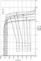
- FIG. 2 is a graph of current (A) vs. voltage (V) illustrating the consequences of using the GaInP BSF 110a in the middle cell of the baseline solar cell 100a.
- A current
- V voltage
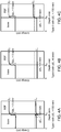
- FIGS. 3A and 3B are graphs providing a comparison of bandgap diagrams for the AlGaAs BSF 110b and the GaInP BSF 110a, both of which form a heterojunction with the GaInAs base 112.
- modeling indicates that the AlGaAs BSF 110b forms a heterojunction with the middle cell base 112 having a lower barrier height of about 90 meV or less in the valence band, as compared to the GaInP BSF 110a.
- the lower barrier height allows for thermalization of majority carrier holes down to much lower temperatures, i.e., temperatures less than about -50°C, which eliminates resistive losses associated with the barrier.
- the GaInP BSF 110a forms a significantly higher heterojunction barrier height of 300 meV in the valance band.
- the GaInP BSF 110a forms a significantly higher heterojunction barrier height of 300 meV in the valance band.
- temperatures above -50°C there is sufficient thermal energy for majority carrier holes to thermalize over this barrier.
- temperatures less than -50°C there is insufficient thermal energy, causing heterojunction resistance that manifests itself in the form a nonlinear behavior in the solar cell 100a LIV curve near Voc. Therefore, increasing doping does not eliminate the issue.
- FIGS. 4A, 4B and 4C are graphs showing possible band alignments for different material situations that improve low-temperature performance, e.g., below -50°C.
- FIG. 4A shows a similar case to that in FIG. 3A with a type-I offset where the valence band is near to that of the base material and a small offset of less than 100 meV is obtained. This limit is important as at temperatures below -50°C, the energy of the hole to surmount the barrier is approximately no more than five times the standard thermal energy of kT or 19.3 meV at -50°C.
- FIG. 4B shows a potential design where no offset occurs in the valence band between the base and BSF.
- FIG. 4C shows a potential design where the offset is type-II and there is a negative offset and the BSF valence band energy is higher than that of the base material.
- BSF materials for GaAs or GaInAs base subcells would be best chosen from materials that follow the main criteria: first, they must have a valence band offset of below 100 meV; second, they may be either type-I or type-II band alignment relative to the base; and third, they must maintain a band offset of greater than 0 meV for the conduction band so that they continue to act as a hetero-step passivation layer and reflect minority carrier electrons away from the interface and back to the p-n junction to be collected.
- the choice of material is superior if a lattice constant of the BSF is near or about the same as a lattice constant of the base. This criterion allows for the smallest number of defects to be created at the interface and the BSF reduces the interfacial recombination velocity of the minority carriers.
- the best choices for BSF materials could be selected from: Al x Ga 1-x As, where x is less than 0.8; Al x Ga 1-x-y In y As, where x is less than 0.8 and y is chosen to allow the alloy BSF to approximately match the base material lattice constant; Al x Ga 1-x As 1-y Sb y , where x is less than 0.8 and y is chosen to match the type-I or type-II alignment.
- Various other combinations may be chosen from multinary alloys of GaNAs, AlGaAs, AlGaAsSb, AlGaPAs, AlGaPAsSb, AlGaInAs, AlGaInPAs, AlGaInPAsSb, AlGaAsBi, AlGaInPAsBi, BGaAs, BAlGaAs, BAlGaInAs, etc., and further examples of material alloys of combinations above. Further combinations may be proposed for subcells of other base materials, such as GaInP, AlGaInP, AlGaInAs, GaInNAs, GaInNAsSb, InPGaInAs, and GaAsSb, so long as the criteria outlined above are followed.
- FIG. 5 is a graph of current (A) vs. voltage (V) illustrating the effect of the reduced heterojunction barrier on the new solar cell's 100b performance.
- A current
- V voltage
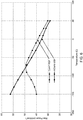
- FIG. 6 is a graph of maximum power (mW/cm 2 ) vs. temperature (C) that compares the baseline solar cell 100a with the GaInP BSF 110a to the new solar cell 100b with the AlGaAs BSF 110b.
- the efficiency increases due to the increasing voltage for the baseline solar cell 100a from room temperature to -50°C. From temperatures of -50°C to -150°C, the efficiency of the baseline solar cell 100a decreases with decreasing temperature due to the high heterojunction resistance and associated non-linearities near Voc.
- the efficiency of the new solar cell 100b increases monotonically with decreasing temperature for a temperature range between room temperature of about 20°C to 30°C and a temperature of about -150°C. This sharply contrasting behavior results in a divergence in low temperature cell performance starting at -50°C. At -150°C, the difference in new solar cell 100b efficiency is 25%, which is a significant improvement for solar cells 100a, 100b that operate in these conditions.
- AlGaAs and InAlGaAs are the materials studied most in depth thus far, multiple other potential materials could also be used.
- Compositions of AlGaAs other than Al 0.2 Ga 0.8 As and InAlGaAs other than In 0.01 Al 0.2 Ga 0.8 As may be used, as well as InGaAsP alloy lattice matched to Ge/GaAs substrates.
- this disclosure describes the widely adopted triple junction solar cell, it could be broadened to cover any instance of a single junction, double junction, or other multiple junction solar cell designed to include materials that lower heterojunction resistance for majority carriers. This would include any BSF-to-base transition or window-to-emitter transition for the valence or conduction bands, respectively.
- any component of the solar cell e.g. the cell, BSF and/or base, may consist of, or consist essentially of, these or other materials.
- this disclosure describes the new solar cell 100b generally, and BSF 110b specifically, as comprising certain materials, alternatives may describe the new solar cell 100b and BSF 110b as consisting of, or consisting essentially of, these or other materials.
- this disclosure describes a new solar cell, such as the new solar cell 100b performing in a desired manner at a temperature of about -50°C or less, alternatives may describe the new solar cell as performing at a temperature of about - 100°C or less, -150°C or less, or other lesser temperatures.
- Examples of the disclosure may be described in the context of a method 700 of fabricating a solar cell, solar cell panel and/or aerospace vehicle such as a satellite, comprising steps 702-714, as shown in FIG. 7A , wherein the resulting satellite 716 comprised of various systems 718 and a body 720, including a panel 722 comprised of an array 724 of one or more solar cells 100b is shown in FIG. 7B .
- exemplary method 700 may include specification and design 702 of the satellite 716, and material procurement 704 for same.
- component and subassembly manufacturing 706 and system integration 708 of the satellite 716 takes place, which include fabricating the satellite 716, panel 722, array 724 and solar cells 100b.
- the satellite 716 may go through certification and delivery 710 in order to be placed in service 712.
- the satellite 716 may also be scheduled for maintenance and service 714 (which includes modification, reconfiguration, refurbishment, and so on), before being launched.
- a system integrator may include without limitation any number of manufacturers and major-system subcontractors; a third party may include without limitation any number of venders, subcontractors, and suppliers; and an operator may be a satellite company, military entity, service organization, and so on.
- the satellite 716 fabricated by exemplary method 700 may include various systems 718 and a body 720.
- the systems 718 included with the satellite 716 include, but are not limited to, one or more of a propulsion system 726, an electrical system 728, a communications system 730, and a power system 732. Any number of other systems also may be included.
- FIG. 8 is an illustration of the panel 722 in the form of a functional block diagram, according to one example.
- the panel 722 is comprised of the array 724, which is comprised of one or more of the solar cells 100b individually attached to the panel 722.
- At least one of the solar cells 100b has an AlGaAs BSF 110b.
- Each of the solar cells 100b absorbs light 800 from a light source 802 and generates an electrical output 804 in response thereto.
Landscapes
- Photovoltaic Devices (AREA)
- Life Sciences & Earth Sciences (AREA)
- Engineering & Computer Science (AREA)
- Sustainable Energy (AREA)
Abstract
Description
- The disclosure is related generally to a solar cell design for improved performance at low temperature.
- While standard space-based solar cell are used on missions that operate near or above room temperature, a variety of new applications for solar cells now require operation at temperatures well below -50°C.
- For example, UAVs (unmanned aerial vehicles) can operate at altitudes greater than 50,000 feet where temperatures approach -70°C. In another example, deep space exploration to Jupiter and Saturn operates between -140 to -165°C.
- As such, solar cell performance at low temperatures is critical for these increasingly common applications. Unfortunately, many solar cells are optimized for near room temperature performance, with significant losses in performance at low temperatures.
- Thus, there is a need for solar cell designs for devices optimized for operation at temperatures less than about -50°C.
- The present disclosure describes a device comprising: a panel including at least one solar cell having a cell comprised of gallium arsenide (GaAs) or indium gallium arsenide (InGaAs) with a back surface field (BSF) comprised of aluminum gallium arsenide (AlGaAs) or indium aluminum gallium arsenide (InAlGaAs) p-type doped for enhanced operation of the solar cell at temperatures less than about -50°C.
- The back surface field may comprise AlxGa1-xAs or In0.01AlxGa1-xAs, wherein x is less than about 0.8, for example, wherein x = 0.2. The back surface field may be p-type doped with zinc (Zn) or carbon (C).
- The back surface field may form a heterojunction with a middle cell (MC) base having a lower barrier height as compared to a middle cell back surface field comprised of gallium indium phosphide (GaInP).
- The back surface field may form a heterojunction with a middle cell base having a barrier height of about 90 meV or less in a valance band. The barrier height allows for thermalization of majority carrier holes down to temperatures less than about -50°C, which eliminates resistive losses associated with the barrier. The barrier height eliminates resistive losses.
- The solar cell's efficiency increases monotonically with decreasing temperature for a temperature range between room temperature and a temperature of about -150°C.
- The present disclosure also describes a method comprising: fabricating a panel including at least one solar cell having a middle cell back surface field comprised of aluminum gallium arsenide doped with zinc for enhanced operation of the solar cell at temperatures less than about -50°C.
- In addition, the present disclosure describes a method comprising: generating a current using a panel including at least one solar cell having a cell comprised of gallium arsenide (GaAs) or indium gallium arsenide (InGaAs) with a back surface field comprised of aluminum gallium arsenide (AlGaAs) or indium aluminum gallium arsenide (InAlGaAs) p-type doped for enhanced operation of the solar cell at temperatures less than about -50°C.
- Finally, the present disclosure describes a device comprising: a panel including at least one solar cell having a middle cell base and a middle cell back surface field for enhanced operation of the solar cell at temperatures less than about -50°C; wherein the base is comprised of gallium arsenide (GaAs) or gallium indium arsenide (GaInAs), and the back surface field is comprised of a material, such that: the back surface field has a valence band offset of below about 100 meV relative to the base; the back surface field has either a type-I or type-II band alignment relative to the base; and the back surface field maintains a conduction band offset of greater than about 0 meV relative to the base, so that the back surface field acts as a hetero-step passivation layer and reflects minority carrier electrons back to a p-n junction to be collected.
- A lattice constant of the base surface field may be about the same as a lattice constant of the middle cell base.
- The back surface field may be comprised of AlxGa1-xAs, where x is less than about 0.8.
- The back surface field may be comprised of aluminum gallium indium arsenide (AlxGa1-x-yInyAs), where x is less than about 0.8 and y is chosen so that a lattice constant of the back surface field is about the same as a lattice constant of the base.
- The back surface field may be comprised of aluminum gallium arsenide antimony (AlxGa1-xAs1-ySby), where x is less than about 0.8 and y is chosen to match the type-I or type-II band alignment relative to the base.
- In each instance, a space vehicle may include the panel.
- Referring now to the drawings in which like reference numbers represent corresponding parts throughout:
-
FIGS. 1A and 1B are layer schematics of triple junction solar cells, illustrating a baseline solar cell inFIG. 1A and a new solar cell inFIG. 1B . -
FIG. 2 is a graph of LIV (light-current-voltage) curves measured from -150°C to 30°C for the baseline solar cell. -
FIGS. 3A and 3B are graphs providing a comparison of bandgap diagrams for the back surface fields of the new and baseline solar cells to a base heterojunction. -
FIGS. 4A, 4B and 4C are graphs showing possible band alignments for different material situations that improve low-temperature performance. -
FIG. 5 is a graph of LIV curves measured from -150°C to 30°C for the new solar cell. -
FIG. 6 is a graph of maximum power as a function of temperature for the back surface fields of the baseline and new solar cells. -
FIG. 7A illustrates a method of fabricating a solar cell, solar cell panel and/or satellite. -
FIG. 7B illustrates a resulting satellite having a solar cell panel comprised of solar cells. -
FIG. 8 is an illustration of the solar cell panel in the form of a functional block diagram. - In the following description, reference is made to the accompanying drawings which form a part hereof, and in which is shown by way of illustration a specific example in which the disclosure may be practiced. It is to be understood that other examples may be utilized and structural changes may be made without departing from the scope of the present disclosure.
- This disclosure describes a design rule for solar cells that improves their performance at low temperatures, for example, less than -50°C.
- Specifically, the main constraint in low temperature performance is the presence of heterojunction resistance that increases exponentially with decreasing temperature. The main heterojunction resistance in a standard triple junction (3J) solar cell occurs between a middle cell base and BSF. The offset in materials in the valence band acts as a rectification diode. At nominal operating temperatures, the barrier is easily surmounted by photogenerated holes to be collected in the circuit. At low temperatures, the interrupt, or hetero-step, in the valence band energies acts as a rectification barrier.
- There have been previous attempts to address this issue of 3J solar cell performance at low temperatures.
- One attempt was to use the standard 3J space solar cells in low temperatures and tolerate any low temperature performance degradations.
- Another attempt was to change the p-type doping in the middle cell base near an interface with the middle cell BSF. Changes in doping can narrow the width of the heterojunction barrier, allowing for increased tunneling transport across the heterojunction barrier and reduced heterojunction resistance. This mitigates the issue, but is tenuous at best depending on the temperature and exact doping level.
- This disclosure reduces this heterojunction resistance by replacing the baseline BSF material to reduce, eliminate, or re-orient the heterojunction barrier. Specifically, one example described in this disclosure describes a new solar cell having a middle cell BSF comprised of AlGaAs or InAlGaAs for improving performance of the solar cell at temperatures less than about -50°C. In one example, the new BSF comprises AlxGa1-xAs or In0.01AlxGa1-xAs, wherein x = 0.2.
- Experimental data demonstrates an increase in efficiency of 25% for the new BSF at -150°C relative to the baseline BSF. In fact, the new solar cell performance is 20-30% greater than the baseline solar cell.
-
FIGS. 1A and 1B are layer schematics, each showing a cross-section of a device comprising baseline and new III-V 3Jsolar cells -
FIG. 1A shows the baseline III-V 3Jsolar cell 100a as currently manufactured. Thesolar cell 100a includes a 5-15 mΩ p-doped germanium (p-Ge)substrate 102, upon which is deposited and/or fabricated a standard (std)nucleation layer 104, abuffer layer 106, alower tunnel junction 108, aGaInP BSF 110a that is doped with Zn, a middle cell (MC) comprised of aGaInAs base 112 and anInGaAs emitter 114, anMC window 116, atop tunnel junction 118, a top cell (TC)BSF 120 that is comprised of GaInP, a TC comprised ofGaInP 122, an aluminum indium phosphide (AlInP)window 124, and aGaInAs cap 126. -
FIG. 1B shows the new III-V 3Jsolar cell 100b according to this disclosure, which substitutes anAlGaAs BSF 110b that is p-type doped with Zn, for theGaInP BSF 110a in the middle cell of the baselinesolar cell 100a. In one example, theBSF 110b comprises AlxGa1-xAs, wherein x = 0.2. In an alternative example, theBSF 110b may comprise In0.01AlxGa1-xAs, wherein x = 0.2. In an alternative example, theBSF 110b may be p-type doped with carbon (C).Thesolar cells -
FIG. 2 is a graph of current (A) vs. voltage (V) illustrating the consequences of using theGaInP BSF 110a in the middle cell of the baselinesolar cell 100a. From room temperature down to -50°C, the LIV curves are well behaved, with linear behavior near Voc (open circuit voltage). The efficiency increases with decreasing temperature in this range due to the increasing Voc. However, for temperatures less than -50°C, the LIV show non-linearities near the Voc. These non-linearities result in losses in the fill factor and significant losses insolar cell 100a performance. This non-linearity is caused by a leaky diode rectification. -
FIGS. 3A and 3B are graphs providing a comparison of bandgap diagrams for theAlGaAs BSF 110b and theGaInP BSF 110a, both of which form a heterojunction with theGaInAs base 112. - As shown in
FIG. 3A , modeling indicates that theAlGaAs BSF 110b forms a heterojunction with themiddle cell base 112 having a lower barrier height of about 90 meV or less in the valence band, as compared to theGaInP BSF 110a. The lower barrier height allows for thermalization of majority carrier holes down to much lower temperatures, i.e., temperatures less than about -50°C, which eliminates resistive losses associated with the barrier. - As shown in
FIG. 3B , theGaInP BSF 110a forms a significantly higher heterojunction barrier height of 300 meV in the valance band. At temperatures above -50°C, there is sufficient thermal energy for majority carrier holes to thermalize over this barrier. At temperatures less than -50°C, there is insufficient thermal energy, causing heterojunction resistance that manifests itself in the form a nonlinear behavior in thesolar cell 100a LIV curve near Voc. Therefore, increasing doping does not eliminate the issue. -
FIGS. 4A, 4B and 4C are graphs showing possible band alignments for different material situations that improve low-temperature performance, e.g., below -50°C. -
FIG. 4A shows a similar case to that inFIG. 3A with a type-I offset where the valence band is near to that of the base material and a small offset of less than 100 meV is obtained. This limit is important as at temperatures below -50°C, the energy of the hole to surmount the barrier is approximately no more than five times the standard thermal energy of kT or 19.3 meV at -50°C. -
FIG. 4B shows a potential design where no offset occurs in the valence band between the base and BSF. -
FIG. 4C shows a potential design where the offset is type-II and there is a negative offset and the BSF valence band energy is higher than that of the base material. Again, a limitation of near 100 meV exists for a type-II band alignment material as the hetero-step offset will form a rectification barrier. - For material selection, the actual energy level of the BSF material varies and are well understood by those skilled in the art of III-V semiconductor devices. Selection of BSF materials for GaAs or GaInAs base subcells would be best chosen from materials that follow the main criteria: first, they must have a valence band offset of below 100 meV; second, they may be either type-I or type-II band alignment relative to the base; and third, they must maintain a band offset of greater than 0 meV for the conduction band so that they continue to act as a hetero-step passivation layer and reflect minority carrier electrons away from the interface and back to the p-n junction to be collected.
- Lastly, the choice of material is superior if a lattice constant of the BSF is near or about the same as a lattice constant of the base. This criterion allows for the smallest number of defects to be created at the interface and the BSF reduces the interfacial recombination velocity of the minority carriers.
- As an example for GaAs and GaInAs, the best choices for BSF materials could be selected from: AlxGa1-xAs, where x is less than 0.8; AlxGa1-x-yInyAs, where x is less than 0.8 and y is chosen to allow the alloy BSF to approximately match the base material lattice constant; AlxGa1-xAs1-ySby, where x is less than 0.8 and y is chosen to match the type-I or type-II alignment. Various other combinations may be chosen from multinary alloys of GaNAs, AlGaAs, AlGaAsSb, AlGaPAs, AlGaPAsSb, AlGaInAs, AlGaInPAs, AlGaInPAsSb, AlGaAsBi, AlGaInPAsBi, BGaAs, BAlGaAs, BAlGaInAs, etc., and further examples of material alloys of combinations above. Further combinations may be proposed for subcells of other base materials, such as GaInP, AlGaInP, AlGaInAs, GaInNAs, GaInNAsSb, InPGaInAs, and GaAsSb, so long as the criteria outlined above are followed.
-
FIG. 5 is a graph of current (A) vs. voltage (V) illustrating the effect of the reduced heterojunction barrier on the new solar cell's 100b performance. In contrast to the baselinesolar cell 100a with theGaInP BSF 110a illustrated inFIG. 2 , the newsolar cell 100b with theAlGaAs BSF 110b shows well behaved LIV curves, particularly near Voc, down to the lowest measured temperature of -150°C. The newsolar cell 100b with theAlGaAs BSF 110b still exhibits increasing Voc with decreasing temperature. -
FIG. 6 is a graph of maximum power (mW/cm2) vs. temperature (C) that compares the baselinesolar cell 100a with theGaInP BSF 110a to the newsolar cell 100b with theAlGaAs BSF 110b. - For the
GaInP BSF 110a case, the efficiency increases due to the increasing voltage for the baselinesolar cell 100a from room temperature to -50°C. From temperatures of -50°C to -150°C, the efficiency of the baselinesolar cell 100a decreases with decreasing temperature due to the high heterojunction resistance and associated non-linearities near Voc. - For the
AlGaAs BSF 110b case, the efficiency of the newsolar cell 100b increases monotonically with decreasing temperature for a temperature range between room temperature of about 20°C to 30°C and a temperature of about -150°C. This sharply contrasting behavior results in a divergence in low temperature cell performance starting at -50°C. At -150°C, the difference in newsolar cell 100b efficiency is 25%, which is a significant improvement forsolar cells - The description set forth above has been presented for purposes of illustration and description, and is not intended to be exhaustive or limited to the examples described. Many alternatives and modifications may be used in place of the specific description set forth above.
- For example, although AlGaAs and InAlGaAs are the materials studied most in depth thus far, multiple other potential materials could also be used. Compositions of AlGaAs other than Al0.2Ga0.8As and InAlGaAs other than In0.01Al0.2Ga0.8As may be used, as well as InGaAsP alloy lattice matched to Ge/GaAs substrates.
- In another example, although this disclosure describes the widely adopted triple junction solar cell, it could be broadened to cover any instance of a single junction, double junction, or other multiple junction solar cell designed to include materials that lower heterojunction resistance for majority carriers. This would include any BSF-to-base transition or window-to-emitter transition for the valence or conduction bands, respectively.
- Although this disclosure describes a solar cell having components comprised of certain materials, in other examples any component of the solar cell, e.g. the cell, BSF and/or base, may consist of, or consist essentially of, these or other materials. Accordingly, in yet another example, although this disclosure describes the new
solar cell 100b generally, andBSF 110b specifically, as comprising certain materials, alternatives may describe the newsolar cell 100b andBSF 110b as consisting of, or consisting essentially of, these or other materials. - Similarly, although this disclosure describes a new solar cell, such as the new
solar cell 100b performing in a desired manner at a temperature of about -50°C or less, alternatives may describe the new solar cell as performing at a temperature of about - 100°C or less, -150°C or less, or other lesser temperatures. - Examples of the disclosure may be described in the context of a
method 700 of fabricating a solar cell, solar cell panel and/or aerospace vehicle such as a satellite, comprising steps 702-714, as shown inFIG. 7A , wherein the resultingsatellite 716 comprised ofvarious systems 718 and abody 720, including apanel 722 comprised of anarray 724 of one or moresolar cells 100b is shown inFIG. 7B . - As illustrated in
FIG. 7A , during pre-production,exemplary method 700 may include specification anddesign 702 of thesatellite 716, andmaterial procurement 704 for same. During production, component andsubassembly manufacturing 706 andsystem integration 708 of thesatellite 716 takes place, which include fabricating thesatellite 716,panel 722,array 724 andsolar cells 100b. Thereafter, thesatellite 716 may go through certification anddelivery 710 in order to be placed inservice 712. Thesatellite 716 may also be scheduled for maintenance and service 714 (which includes modification, reconfiguration, refurbishment, and so on), before being launched. - Each of the processes of
method 700 may be performed or carried out by a system integrator, a third party, and/or an operator (e.g., a customer). For the purposes of this description, a system integrator may include without limitation any number of manufacturers and major-system subcontractors; a third party may include without limitation any number of venders, subcontractors, and suppliers; and an operator may be a satellite company, military entity, service organization, and so on. - As shown in
FIG. 7B , thesatellite 716 fabricated byexemplary method 700 may includevarious systems 718 and abody 720. Examples of thesystems 718 included with thesatellite 716 include, but are not limited to, one or more of apropulsion system 726, anelectrical system 728, acommunications system 730, and apower system 732. Any number of other systems also may be included. -
FIG. 8 is an illustration of thepanel 722 in the form of a functional block diagram, according to one example. Thepanel 722 is comprised of thearray 724, which is comprised of one or more of thesolar cells 100b individually attached to thepanel 722. At least one of thesolar cells 100b has anAlGaAs BSF 110b. Each of thesolar cells 100b absorbs light 800 from alight source 802 and generates anelectrical output 804 in response thereto. - Further, the disclosure comprises examples according to the following clauses:
-
Clause 1. A device, comprising: a panel including at least one solar cell having a cell comprised of gallium arsenide (GaAs) or indium gallium arsenide (InGaAs) with a back surface field (BSF) comprised of aluminum gallium arsenide (AlGaAs) or indium aluminum gallium arsenide (InAlGaAs) p-type doped for enhanced operation of the solar cell at temperatures less than about -50°C. -
Clause 2. The device ofClause 1, wherein the back surface field is comprised of AlxGal-xAs or In0.01AlxGa1-xAs. -
Clause 3. The device ofClause 2, wherein x is less than about 0.8. -
Clause 4. The device ofClause 3, wherein x = 0.2. - Clause 5. The device of any of Clauses 1-4, wherein the back surface field is p-type doped with zinc (Zn) or carbon (C).
- Clause 6. The device of any of Clauses 1-5, wherein the back surface field forms a heterojunction with a middle cell base having a lower barrier height as compared to a middle cell back surface field comprised of gallium indium phosphide (GaInP).
- Clause 7. The device of any of Clauses 1-6, wherein the back surface field forms a heterojunction with a middle cell base having a barrier height of about 90 meV or less in a valance band.
- Clause 8. The device of Clause 7, wherein the barrier height allows for thermalization of majority carrier holes down to temperatures less than about -50°C, which eliminates resistive losses associated with the barrier.
- Clause 9. The device of Clause 7 or 8, wherein the barrier height eliminates resistive losses.
- Clause 10. The device of any of Clauses 1-9, wherein the solar cell's efficiency increases monotonically with decreasing temperature for a temperature range between room temperature and a temperature of about -150°C.
- Clause 11. The device of any of Clauses 1-10, further comprising a space vehicle including the panel.
- Clause 12. A method, comprising: fabricating a panel including at least one solar cell having a cell comprised of gallium arsenide (GaAs) or indium gallium arsenide (InGaAs) with a back surface field comprised of aluminum gallium arsenide (AlGaAs) or indium aluminum gallium arsenide (InAlGaAs) p-type doped for enhanced operation of the solar cell at temperatures less than about -50°C.
- Clause 13. The method of Clause 12, wherein the back surface field is comprised of AlxGa1-xAs or In0.01AlxGa1-xAs, where x is less than about 0.8.
- Clause 14. The method of Clause 12 or 13, wherein the back surface field is p-type doped with zinc (Zn) or carbon (C).
- Clause 15. A method, comprising: generating a current using a panel including at least one solar cell having a cell comprised of gallium arsenide (GaAs) or indium gallium arsenide (InGaAs) with a back surface field comprised of aluminum gallium arsenide (AlGaAs) or indium aluminum gallium arsenide (InAlGaAs) p-type doped for enhanced operation of the solar cell at temperatures less than about -50°C.
- Clause 16. The device of Clause 15, wherein the back surface field is comprised of AlxGa1-xAs or In0.01AlxGa1-xAs, where x is less than about 0.8.
- Clause 17. A device, comprising: a panel including at least one solar cell having a middle cell (MC) base and a middle cell back surface field (BSF) for enhanced operation of the solar cell at temperatures less than about -50°C; wherein the base is comprised of gallium arsenide (GaAs) or gallium indium arsenide (GaInAs), and the back surface field is comprised of a material, such that: the back surface field has a valence band offset of below about 100 meV relative to the base; the back surface field has either a type-I or type-II band alignment relative to the base; and the back surface field maintains a conduction band offset of greater than about 0 meV relative to the base, so that the back surface field acts as a hetero-step passivation layer and reflects minority carrier electrons back to a p-n junction to be collected.
- Clause 18. The device of Clause 17, wherein a lattice constant of the base surface field is about the same as a lattice constant of the middle cell base.
- Clause 19. The device of Clause 17 or 18, wherein the back surface field is comprised of aluminum gallium arsenide (AlxGa1-xAs), where x is less than about 0.8.
- Clause 20. The device of any of Clauses 17-19, wherein the back surface field is comprised of aluminum gallium indium arsenide (AlxGa1-x-yInyAs), where x is less than about 0.8 and y is chosen so that a lattice constant of the back surface field is about the same as a lattice constant of the base.
- Clause 21. The device of any of Clauses 17-19, wherein the back surface field is comprised of aluminum gallium arsenide antimony (AlxGa1-xAs1-ySby), where x is less than about 0.8 and y is chosen to match the type-I or type-II band alignment relative to the base.
Claims (15)
- A device, comprising:
a panel including at least one solar cell having a cell comprised of gallium arsenide (GaAs) or indium gallium arsenide (InGaAs) with a back surface field (BSF) comprised of aluminum gallium arsenide (AlGaAs) or indium aluminum gallium arsenide (InAlGaAs) p-type doped for enhanced operation of the solar cell at temperatures less than about -50°C. - The device of claim 1, wherein the back surface field is comprised of AlxGa1-xAs or In0.01AlxGa1-xAs.
- The device of claim 2, wherein x is less than about 0.8, preferably wherein x = 0.2.
- The device of any of claims 1-3, wherein the back surface field is p-type doped with zinc (Zn) or carbon (C).
- The device of any of claims 1-4, wherein the back surface field forms a heterojunction with a middle cell base having a lower barrier height as compared to a middle cell back surface field comprised of gallium indium phosphide (GaInP).
- The device of any of claims 1-5, wherein the back surface field forms a heterojunction with a middle cell base having a barrier height of about 90 meV or less in a valance band.
- The device of claim 6, wherein the barrier height allows for thermalization of majority carrier holes down to temperatures less than about -50°C, which eliminates resistive losses associated with the barrier and/or wherein the barrier height eliminates resistive losses.
- The device of any of claims 1-7, wherein the solar cell's efficiency increases monotonically with decreasing temperature for a temperature range between room temperature and a temperature of about -150°C and/or wherein the device further comprises a space vehicle including the panel.
- A method, comprising:
fabricating a panel including at least one solar cell having a cell comprised of gallium arsenide (GaAs) or indium gallium arsenide (InGaAs) with a back surface field comprised of aluminum gallium arsenide (AlGaAs) or indium aluminum gallium arsenide (InAlGaAs) p-type doped for enhanced operation of the solar cell at temperatures less than about -50°C, wherein the back surface field is preferably comprised of AlxGa1-xAs or In0.01AlxGa1-xAs, where x is less than about 0.8. - The method of claim 9, wherein the back surface field is p-type doped with zinc (Zn) or carbon (C).
- A method, comprising:
generating a current using a panel including at least one solar cell having a cell comprised of gallium arsenide (GaAs) or indium gallium arsenide (InGaAs) with a back surface field comprised of aluminum gallium arsenide (AlGaAs) or indium aluminum gallium arsenide (InAlGaAs) p-type doped for enhanced operation of the solar cell at temperatures less than about -50°C, wherein the back surface field is preferably comprised of AlxGa1-xAs or In0.01AlxGa1-xAs, where x is less than about 0.8. - A device, comprising:a panel including at least one solar cell having a middle cell (MC) base and a middle cell back surface field (BSF) for enhanced operation of the solar cell at temperatures less than about -50°C;wherein the base is comprised of gallium arsenide (GaAs) or gallium indium arsenide (GaInAs), and the back surface field is comprised of a material, such that:the back surface field has a valence band offset of below about 100 meV relative to the base;the back surface field has either a type-I or type-II band alignment relative to the base; andthe back surface field maintains a conduction band offset of greater than about 0 meV relative to the base, so that the back surface field acts as a hetero-step passivation layer and reflects minority carrier electrons back to a p-n junction to be collected.
- The device of claim 12, wherein a lattice constant of the base surface field is about the same as a lattice constant of the middle cell base.
- The device of claim 12 or 13, wherein the back surface field is comprised of aluminum gallium arsenide (AlxGa1-xAs), where x is less than about 0.8.
- The device of claim 12 or 13, wherein the back surface field is comprised of aluminum gallium indium arsenide (AlxGa1-x-yInyAs), where x is less than about 0.8 and y is chosen so that a lattice constant of the back surface field is about the same as a lattice constant of the base, or wherein the back surface field is comprised of aluminum gallium arsenide antimony (AlxGa1-xAs1-ySby), where x is less than about 0.8 and y is chosen to match the type-I or type-II band alignment relative to the base.
Applications Claiming Priority (2)
| Application Number | Priority Date | Filing Date | Title |
|---|---|---|---|
| US201962836453P | 2019-04-19 | 2019-04-19 | |
| US16/786,841 US12593514B2 (en) | 2019-04-19 | 2020-02-10 | Solar cell design for improved performance at low temperature |
Publications (1)
| Publication Number | Publication Date |
|---|---|
| EP3726591A1 true EP3726591A1 (en) | 2020-10-21 |
Family
ID=69699796
Family Applications (1)
| Application Number | Title | Priority Date | Filing Date |
|---|---|---|---|
| EP20158010.7A Pending EP3726591A1 (en) | 2019-04-19 | 2020-02-18 | Solar cell design for improved performance at low temperature |
Country Status (4)
| Country | Link |
|---|---|
| US (1) | US12593514B2 (en) |
| EP (1) | EP3726591A1 (en) |
| JP (1) | JP2020178116A (en) |
| CN (1) | CN111834485A (en) |
Citations (4)
| Publication number | Priority date | Publication date | Assignee | Title |
|---|---|---|---|---|
| US20150104898A1 (en) * | 2013-10-11 | 2015-04-16 | Emcore Solar Power, Inc. | Method for manufacturing inverted metamorphic multijunction solar cells |
| CN104300015B (en) * | 2014-10-13 | 2017-01-18 | 北京工业大学 | AlGaAs/GaInAs/Ge continuous spectrum solar battery |
| US9842957B1 (en) * | 2016-05-04 | 2017-12-12 | The United States Of America, As Represented By The Secretary Of The Navy | AlGaAs/GaAs solar cell with back-surface alternating contacts (GaAs BAC solar cell) |
| CN106067493B (en) * | 2016-07-26 | 2018-05-22 | 中山德华芯片技术有限公司 | Micro-lattice mismatch quantum well solar cell and preparation method thereof |
Family Cites Families (10)
| Publication number | Priority date | Publication date | Assignee | Title |
|---|---|---|---|---|
| US4195305A (en) | 1978-09-25 | 1980-03-25 | Varian Associates, Inc. | Lattice constant grading in the Aly Ga1-y As1-x Sbx alloy system |
| US7122734B2 (en) * | 2002-10-23 | 2006-10-17 | The Boeing Company | Isoelectronic surfactant suppression of threading dislocations in metamorphic epitaxial layers |
| US20090229662A1 (en) * | 2008-03-13 | 2009-09-17 | Emcore Corporation | Off-Cut Substrates In Inverted Metamorphic Multijunction Solar Cells |
| KR20150006452A (en) * | 2012-04-23 | 2015-01-16 | 난양 테크놀러지컬 유니버시티 | A cell arrangement |
| WO2013192559A1 (en) * | 2012-06-22 | 2013-12-27 | Izar Solar Inc | Manufacturing semiconductor-based multi-junction photovoltaic devices |
| CN104300150A (en) | 2014-05-07 | 2015-01-21 | 河南中联高科新能源有限公司 | Asphalt-based nanoporous carbon material, negative material thereof, and lithium ion battery |
| DE102015009004A1 (en) * | 2015-06-05 | 2016-12-08 | Solaero Technologies Corp. | Automated arrangement and mounting of solar cells on panels for space applications |
| US10361330B2 (en) | 2015-10-19 | 2019-07-23 | Solaero Technologies Corp. | Multijunction solar cell assemblies for space applications |
| US10270000B2 (en) | 2015-10-19 | 2019-04-23 | Solaero Technologies Corp. | Multijunction metamorphic solar cell assembly for space applications |
| US20190181289A1 (en) * | 2017-12-11 | 2019-06-13 | Solaero Technologies Corp. | Multijunction solar cells |
-
2020
- 2020-02-10 US US16/786,841 patent/US12593514B2/en active Active
- 2020-02-18 EP EP20158010.7A patent/EP3726591A1/en active Pending
- 2020-02-18 CN CN202010098706.1A patent/CN111834485A/en active Pending
- 2020-02-18 JP JP2020024978A patent/JP2020178116A/en active Pending
Patent Citations (4)
| Publication number | Priority date | Publication date | Assignee | Title |
|---|---|---|---|---|
| US20150104898A1 (en) * | 2013-10-11 | 2015-04-16 | Emcore Solar Power, Inc. | Method for manufacturing inverted metamorphic multijunction solar cells |
| CN104300015B (en) * | 2014-10-13 | 2017-01-18 | 北京工业大学 | AlGaAs/GaInAs/Ge continuous spectrum solar battery |
| US9842957B1 (en) * | 2016-05-04 | 2017-12-12 | The United States Of America, As Represented By The Secretary Of The Navy | AlGaAs/GaAs solar cell with back-surface alternating contacts (GaAs BAC solar cell) |
| CN106067493B (en) * | 2016-07-26 | 2018-05-22 | 中山德华芯片技术有限公司 | Micro-lattice mismatch quantum well solar cell and preparation method thereof |
Non-Patent Citations (1)
| Title |
|---|
| WALKER ALEXANDRE W ET AL: "Impact of photon recycling and luminescence coupling on III-V single and dual junction photovoltaic devices", JOURNAL OF PHOTONICS FOR ENERGY, SOCIETY OF PHOTO-OPTICAL INSTRUMENTATION ENGINEERS, 1000 20TH ST. BELLINGHAM WA 98225-6705 USA, vol. 5, no. 1, 1 January 2015 (2015-01-01), pages 53087, XP060072785, DOI: 10.1117/1.JPE.5.053087 * |
Also Published As
| Publication number | Publication date |
|---|---|
| JP2020178116A (en) | 2020-10-29 |
| US20200335652A1 (en) | 2020-10-22 |
| US12593514B2 (en) | 2026-03-31 |
| CN111834485A (en) | 2020-10-27 |
Similar Documents
| Publication | Publication Date | Title |
|---|---|---|
| US6586669B2 (en) | Lattice-matched semiconductor materials for use in electronic or optoelectronic devices | |
| US8895342B2 (en) | Heterojunction subcells in inverted metamorphic multijunction solar cells | |
| US20210305448A1 (en) | Multijunction metamorphic solar cells | |
| US20100006143A1 (en) | Solar Cell Devices | |
| US11527667B2 (en) | Tunnel junctions for multijunction solar cells | |
| US20170054048A1 (en) | Four junction solar cell for space applications | |
| Choi et al. | High-performance GaInAsSb thermophotovoltaic devices with an AlGaAsSb window | |
| EP3167491B1 (en) | Compound-semiconductor photovoltaic cell and manufacturing method of compound-semiconductor photovoltaic cell | |
| US20120138130A1 (en) | Tunnel diodes comprising stress-compensated compound semiconductor layers | |
| CN102668133A (en) | Multijunction solar cells formed on n-doped substrates | |
| TWI775725B (en) | Antimonide-based high bandgap tunnel junction for semiconductor devices | |
| US12249667B2 (en) | Space vehicles including multijunction metamorphic solar cells | |
| US9722122B2 (en) | Boron, bismuth co-doping of gallium arsenide and other compounds for photonic and heterojunction bipolar transistor devices | |
| TW201907575A (en) | MOCVD/MBE hybrid epitaxial growth of highly efficient and lattice matched multi-junction solar cells | |
| CN102651419A (en) | Quadruple-junction cascading solar battery and fabrication method thereof | |
| Li et al. | > 35% 5-junction space solar cells based on the direct bonding technique | |
| EP3758072A1 (en) | Solar cell design optimized for performance at high radiation doses | |
| US20180182912A1 (en) | Compound semiconductor solar cell | |
| US20200335650A1 (en) | Multijunction metamorphic solar cell for space applications | |
| Kim et al. | Cryogenic GaAs laser power converters | |
| EP3726591A1 (en) | Solar cell design for improved performance at low temperature | |
| EP3726590A1 (en) | Solar cell design for improved performance at low temperature | |
| Chow et al. | Structural and transport properties of InAs/AlSb superlattices | |
| CN103337548A (en) | Structure of Bi containing thermophotovoltaic cell and preparation method of thermophotovoltaic cell | |
| CN114141901A (en) | A germanium-based gallium arsenide solar cell and preparation method thereof |
Legal Events
| Date | Code | Title | Description |
|---|---|---|---|
| PUAI | Public reference made under article 153(3) epc to a published international application that has entered the european phase |
Free format text: ORIGINAL CODE: 0009012 |
|
| STAA | Information on the status of an ep patent application or granted ep patent |
Free format text: STATUS: THE APPLICATION HAS BEEN PUBLISHED |
|
| AK | Designated contracting states |
Kind code of ref document: A1 Designated state(s): AL AT BE BG CH CY CZ DE DK EE ES FI FR GB GR HR HU IE IS IT LI LT LU LV MC MK MT NL NO PL PT RO RS SE SI SK SM TR |
|
| AX | Request for extension of the european patent |
Extension state: BA ME |
|
| STAA | Information on the status of an ep patent application or granted ep patent |
Free format text: STATUS: REQUEST FOR EXAMINATION WAS MADE |
|
| 17P | Request for examination filed |
Effective date: 20210421 |
|
| RBV | Designated contracting states (corrected) |
Designated state(s): AL AT BE BG CH CY CZ DE DK EE ES FI FR GB GR HR HU IE IS IT LI LT LU LV MC MK MT NL NO PL PT RO RS SE SI SK SM TR |
|
| STAA | Information on the status of an ep patent application or granted ep patent |
Free format text: STATUS: EXAMINATION IS IN PROGRESS |
|
| 17Q | First examination report despatched |
Effective date: 20221007 |
|
| RAP3 | Party data changed (applicant data changed or rights of an application transferred) |
Owner name: THE BOEING COMPANY |