EP3725531A1 - Fluid ejection device with reduced number of components, and method for manufacturing the fluid ejection device - Google Patents
Fluid ejection device with reduced number of components, and method for manufacturing the fluid ejection device Download PDFInfo
- Publication number
- EP3725531A1 EP3725531A1 EP20169708.3A EP20169708A EP3725531A1 EP 3725531 A1 EP3725531 A1 EP 3725531A1 EP 20169708 A EP20169708 A EP 20169708A EP 3725531 A1 EP3725531 A1 EP 3725531A1
- Authority
- EP
- European Patent Office
- Prior art keywords
- piezoelectric actuator
- fluid
- forming
- wafer
- ejection device
- Prior art date
- Legal status (The legal status is an assumption and is not a legal conclusion. Google has not performed a legal analysis and makes no representation as to the accuracy of the status listed.)
- Granted
Links
Images




Classifications
-
- B—PERFORMING OPERATIONS; TRANSPORTING
- B41—PRINTING; LINING MACHINES; TYPEWRITERS; STAMPS
- B41J—TYPEWRITERS; SELECTIVE PRINTING MECHANISMS, i.e. MECHANISMS PRINTING OTHERWISE THAN FROM A FORME; CORRECTION OF TYPOGRAPHICAL ERRORS
- B41J2/00—Typewriters or selective printing mechanisms characterised by the printing or marking process for which they are designed
- B41J2/005—Typewriters or selective printing mechanisms characterised by the printing or marking process for which they are designed characterised by bringing liquid or particles selectively into contact with a printing material
- B41J2/01—Ink jet
- B41J2/135—Nozzles
- B41J2/14—Structure thereof only for on-demand ink jet heads
- B41J2/14201—Structure of print heads with piezoelectric elements
-
- B—PERFORMING OPERATIONS; TRANSPORTING
- B41—PRINTING; LINING MACHINES; TYPEWRITERS; STAMPS
- B41J—TYPEWRITERS; SELECTIVE PRINTING MECHANISMS, i.e. MECHANISMS PRINTING OTHERWISE THAN FROM A FORME; CORRECTION OF TYPOGRAPHICAL ERRORS
- B41J2/00—Typewriters or selective printing mechanisms characterised by the printing or marking process for which they are designed
- B41J2/005—Typewriters or selective printing mechanisms characterised by the printing or marking process for which they are designed characterised by bringing liquid or particles selectively into contact with a printing material
- B41J2/01—Ink jet
- B41J2/135—Nozzles
- B41J2/16—Production of nozzles
- B41J2/1607—Production of print heads with piezoelectric elements
- B41J2/161—Production of print heads with piezoelectric elements of film type, deformed by bending and disposed on a diaphragm
-
- B—PERFORMING OPERATIONS; TRANSPORTING
- B41—PRINTING; LINING MACHINES; TYPEWRITERS; STAMPS
- B41J—TYPEWRITERS; SELECTIVE PRINTING MECHANISMS, i.e. MECHANISMS PRINTING OTHERWISE THAN FROM A FORME; CORRECTION OF TYPOGRAPHICAL ERRORS
- B41J2/00—Typewriters or selective printing mechanisms characterised by the printing or marking process for which they are designed
- B41J2/005—Typewriters or selective printing mechanisms characterised by the printing or marking process for which they are designed characterised by bringing liquid or particles selectively into contact with a printing material
- B41J2/01—Ink jet
- B41J2/135—Nozzles
- B41J2/16—Production of nozzles
- B41J2/1621—Manufacturing processes
- B41J2/1623—Manufacturing processes bonding and adhesion
-
- B—PERFORMING OPERATIONS; TRANSPORTING
- B41—PRINTING; LINING MACHINES; TYPEWRITERS; STAMPS
- B41J—TYPEWRITERS; SELECTIVE PRINTING MECHANISMS, i.e. MECHANISMS PRINTING OTHERWISE THAN FROM A FORME; CORRECTION OF TYPOGRAPHICAL ERRORS
- B41J2/00—Typewriters or selective printing mechanisms characterised by the printing or marking process for which they are designed
- B41J2/005—Typewriters or selective printing mechanisms characterised by the printing or marking process for which they are designed characterised by bringing liquid or particles selectively into contact with a printing material
- B41J2/01—Ink jet
-
- B—PERFORMING OPERATIONS; TRANSPORTING
- B41—PRINTING; LINING MACHINES; TYPEWRITERS; STAMPS
- B41J—TYPEWRITERS; SELECTIVE PRINTING MECHANISMS, i.e. MECHANISMS PRINTING OTHERWISE THAN FROM A FORME; CORRECTION OF TYPOGRAPHICAL ERRORS
- B41J2/00—Typewriters or selective printing mechanisms characterised by the printing or marking process for which they are designed
- B41J2/005—Typewriters or selective printing mechanisms characterised by the printing or marking process for which they are designed characterised by bringing liquid or particles selectively into contact with a printing material
- B41J2/01—Ink jet
- B41J2/135—Nozzles
- B41J2/14—Structure thereof only for on-demand ink jet heads
- B41J2/14201—Structure of print heads with piezoelectric elements
- B41J2/14233—Structure of print heads with piezoelectric elements of film type, deformed by bending and disposed on a diaphragm
-
- B—PERFORMING OPERATIONS; TRANSPORTING
- B41—PRINTING; LINING MACHINES; TYPEWRITERS; STAMPS
- B41J—TYPEWRITERS; SELECTIVE PRINTING MECHANISMS, i.e. MECHANISMS PRINTING OTHERWISE THAN FROM A FORME; CORRECTION OF TYPOGRAPHICAL ERRORS
- B41J2/00—Typewriters or selective printing mechanisms characterised by the printing or marking process for which they are designed
- B41J2/005—Typewriters or selective printing mechanisms characterised by the printing or marking process for which they are designed characterised by bringing liquid or particles selectively into contact with a printing material
- B41J2/01—Ink jet
- B41J2/135—Nozzles
- B41J2/14—Structure thereof only for on-demand ink jet heads
- B41J2/1433—Structure of nozzle plates
-
- B—PERFORMING OPERATIONS; TRANSPORTING
- B41—PRINTING; LINING MACHINES; TYPEWRITERS; STAMPS
- B41J—TYPEWRITERS; SELECTIVE PRINTING MECHANISMS, i.e. MECHANISMS PRINTING OTHERWISE THAN FROM A FORME; CORRECTION OF TYPOGRAPHICAL ERRORS
- B41J2/00—Typewriters or selective printing mechanisms characterised by the printing or marking process for which they are designed
- B41J2/005—Typewriters or selective printing mechanisms characterised by the printing or marking process for which they are designed characterised by bringing liquid or particles selectively into contact with a printing material
- B41J2/01—Ink jet
- B41J2/135—Nozzles
- B41J2/16—Production of nozzles
- B41J2/162—Manufacturing of the nozzle plates
-
- B—PERFORMING OPERATIONS; TRANSPORTING
- B41—PRINTING; LINING MACHINES; TYPEWRITERS; STAMPS
- B41J—TYPEWRITERS; SELECTIVE PRINTING MECHANISMS, i.e. MECHANISMS PRINTING OTHERWISE THAN FROM A FORME; CORRECTION OF TYPOGRAPHICAL ERRORS
- B41J2/00—Typewriters or selective printing mechanisms characterised by the printing or marking process for which they are designed
- B41J2/005—Typewriters or selective printing mechanisms characterised by the printing or marking process for which they are designed characterised by bringing liquid or particles selectively into contact with a printing material
- B41J2/01—Ink jet
- B41J2/135—Nozzles
- B41J2/16—Production of nozzles
- B41J2/1621—Manufacturing processes
-
- B—PERFORMING OPERATIONS; TRANSPORTING
- B41—PRINTING; LINING MACHINES; TYPEWRITERS; STAMPS
- B41J—TYPEWRITERS; SELECTIVE PRINTING MECHANISMS, i.e. MECHANISMS PRINTING OTHERWISE THAN FROM A FORME; CORRECTION OF TYPOGRAPHICAL ERRORS
- B41J2/00—Typewriters or selective printing mechanisms characterised by the printing or marking process for which they are designed
- B41J2/005—Typewriters or selective printing mechanisms characterised by the printing or marking process for which they are designed characterised by bringing liquid or particles selectively into contact with a printing material
- B41J2/01—Ink jet
- B41J2/135—Nozzles
- B41J2/16—Production of nozzles
- B41J2/1621—Manufacturing processes
- B41J2/1626—Manufacturing processes etching
-
- B—PERFORMING OPERATIONS; TRANSPORTING
- B41—PRINTING; LINING MACHINES; TYPEWRITERS; STAMPS
- B41J—TYPEWRITERS; SELECTIVE PRINTING MECHANISMS, i.e. MECHANISMS PRINTING OTHERWISE THAN FROM A FORME; CORRECTION OF TYPOGRAPHICAL ERRORS
- B41J2/00—Typewriters or selective printing mechanisms characterised by the printing or marking process for which they are designed
- B41J2/005—Typewriters or selective printing mechanisms characterised by the printing or marking process for which they are designed characterised by bringing liquid or particles selectively into contact with a printing material
- B41J2/01—Ink jet
- B41J2/135—Nozzles
- B41J2/16—Production of nozzles
- B41J2/1621—Manufacturing processes
- B41J2/1626—Manufacturing processes etching
- B41J2/1628—Manufacturing processes etching dry etching
-
- B—PERFORMING OPERATIONS; TRANSPORTING
- B41—PRINTING; LINING MACHINES; TYPEWRITERS; STAMPS
- B41J—TYPEWRITERS; SELECTIVE PRINTING MECHANISMS, i.e. MECHANISMS PRINTING OTHERWISE THAN FROM A FORME; CORRECTION OF TYPOGRAPHICAL ERRORS
- B41J2/00—Typewriters or selective printing mechanisms characterised by the printing or marking process for which they are designed
- B41J2/005—Typewriters or selective printing mechanisms characterised by the printing or marking process for which they are designed characterised by bringing liquid or particles selectively into contact with a printing material
- B41J2/01—Ink jet
- B41J2/135—Nozzles
- B41J2/16—Production of nozzles
- B41J2/1621—Manufacturing processes
- B41J2/1626—Manufacturing processes etching
- B41J2/1629—Manufacturing processes etching wet etching
-
- B—PERFORMING OPERATIONS; TRANSPORTING
- B41—PRINTING; LINING MACHINES; TYPEWRITERS; STAMPS
- B41J—TYPEWRITERS; SELECTIVE PRINTING MECHANISMS, i.e. MECHANISMS PRINTING OTHERWISE THAN FROM A FORME; CORRECTION OF TYPOGRAPHICAL ERRORS
- B41J2/00—Typewriters or selective printing mechanisms characterised by the printing or marking process for which they are designed
- B41J2/005—Typewriters or selective printing mechanisms characterised by the printing or marking process for which they are designed characterised by bringing liquid or particles selectively into contact with a printing material
- B41J2/01—Ink jet
- B41J2/135—Nozzles
- B41J2/16—Production of nozzles
- B41J2/1621—Manufacturing processes
- B41J2/1631—Manufacturing processes photolithography
-
- B—PERFORMING OPERATIONS; TRANSPORTING
- B41—PRINTING; LINING MACHINES; TYPEWRITERS; STAMPS
- B41J—TYPEWRITERS; SELECTIVE PRINTING MECHANISMS, i.e. MECHANISMS PRINTING OTHERWISE THAN FROM A FORME; CORRECTION OF TYPOGRAPHICAL ERRORS
- B41J2/00—Typewriters or selective printing mechanisms characterised by the printing or marking process for which they are designed
- B41J2/005—Typewriters or selective printing mechanisms characterised by the printing or marking process for which they are designed characterised by bringing liquid or particles selectively into contact with a printing material
- B41J2/01—Ink jet
- B41J2/135—Nozzles
- B41J2/16—Production of nozzles
- B41J2/1621—Manufacturing processes
- B41J2/1632—Manufacturing processes machining
-
- B—PERFORMING OPERATIONS; TRANSPORTING
- B41—PRINTING; LINING MACHINES; TYPEWRITERS; STAMPS
- B41J—TYPEWRITERS; SELECTIVE PRINTING MECHANISMS, i.e. MECHANISMS PRINTING OTHERWISE THAN FROM A FORME; CORRECTION OF TYPOGRAPHICAL ERRORS
- B41J2/00—Typewriters or selective printing mechanisms characterised by the printing or marking process for which they are designed
- B41J2/005—Typewriters or selective printing mechanisms characterised by the printing or marking process for which they are designed characterised by bringing liquid or particles selectively into contact with a printing material
- B41J2/01—Ink jet
- B41J2/135—Nozzles
- B41J2/165—Prevention or detection of nozzle clogging, e.g. cleaning, capping or moistening for nozzles
- B41J2/16517—Cleaning of print head nozzles
- B41J2/1652—Cleaning of print head nozzles by driving a fluid through the nozzles to the outside thereof, e.g. by applying pressure to the inside or vacuum at the outside of the print head
-
- B—PERFORMING OPERATIONS; TRANSPORTING
- B41—PRINTING; LINING MACHINES; TYPEWRITERS; STAMPS
- B41J—TYPEWRITERS; SELECTIVE PRINTING MECHANISMS, i.e. MECHANISMS PRINTING OTHERWISE THAN FROM A FORME; CORRECTION OF TYPOGRAPHICAL ERRORS
- B41J2/00—Typewriters or selective printing mechanisms characterised by the printing or marking process for which they are designed
- B41J2/005—Typewriters or selective printing mechanisms characterised by the printing or marking process for which they are designed characterised by bringing liquid or particles selectively into contact with a printing material
- B41J2/01—Ink jet
- B41J2/135—Nozzles
- B41J2/14—Structure thereof only for on-demand ink jet heads
- B41J2/14201—Structure of print heads with piezoelectric elements
- B41J2/14233—Structure of print heads with piezoelectric elements of film type, deformed by bending and disposed on a diaphragm
- B41J2002/14258—Multi layer thin film type piezoelectric element
-
- B—PERFORMING OPERATIONS; TRANSPORTING
- B41—PRINTING; LINING MACHINES; TYPEWRITERS; STAMPS
- B41J—TYPEWRITERS; SELECTIVE PRINTING MECHANISMS, i.e. MECHANISMS PRINTING OTHERWISE THAN FROM A FORME; CORRECTION OF TYPOGRAPHICAL ERRORS
- B41J2/00—Typewriters or selective printing mechanisms characterised by the printing or marking process for which they are designed
- B41J2/005—Typewriters or selective printing mechanisms characterised by the printing or marking process for which they are designed characterised by bringing liquid or particles selectively into contact with a printing material
- B41J2/01—Ink jet
- B41J2/135—Nozzles
- B41J2/14—Structure thereof only for on-demand ink jet heads
- B41J2002/1437—Back shooter
Definitions
- the present invention relates to a method for manufacturing a fluid ejection device and to a fluid ejection device.
- the present invention relates a fluid ejection device, based upon piezoelectric technology, including just two wafers of semiconductor material machined and coupled together.
- Printheads of this sort can likewise be used for ejecting fluids other than ink, for example for applications in the biological or biomedical field, for local application of biological material (e.g., DNA) in the manufacture of sensors for biological analyses, for the decoration of fabrics or ceramics, and in applications of 3D printing and additive production.
- biological material e.g., DNA
- a printhead is typically formed by a large number of fluid ejection devices (of the order of hundreds or thousands), each of which includes a nozzle, a chamber for containing the fluid coupled to the nozzle, and an actuator coupled to the chamber, for causing outlet of the fluid through the respective nozzle. It is desirable for each of the fluid ejection devices belonging to a printhead to be as identical as possible to the other fluid ejection devices belonging to the same printhead, to guarantee uniformity of performance, above all in terms of volume of the fluid ejected and ejection rates.
- the patent document No. US 2017/182778 discloses a method for manufacturing a fluid ejection device that envisages coupling of three wafers at least in part pre-machined.
- the method described envisages coupling steps (e.g., using bonding techniques) that require a high degree of accuracy in order to obtain a good alignment between the wafers and between the functional elements obtained therein.
- formation of the actuation membrane of the ejection device envisages an etching step via which the area of the suspended portion of the membrane is defined. It is evident that devices manufactured at different times and/or with different machinery may be subject to undesired variations of the size of the aforesaid suspended area, with the risk of jeopardising reproducibility of the ejection device.
- the aim of the present invention is to provide a method for manufacturing a fluid ejection device, and a fluid ejection device, that will overcome the drawbacks of the prior art.
- a method for manufacturing a fluid ejection device and a fluid ejection device are provided, as defined in the annexed claims.
- Figure 1 is a side cross-section view, taken along a plane XZ of a triaxial cartesian system X, Y, Z.
- a first wafer 2 including a structural layer 11 of semiconductor material, is machined so as to form thereon one or more piezoelectric actuators 3, adapted to be controlled to generate a deflection of a membrane 7.
- Deflection of the membrane 7 causes a variation in the internal volume of one or more respective chambers 10 adapted to define respective reservoirs for containing a fluid 6 to be expelled during use through an outlet channel 33.
- Figure 1 shows by way of example an individual chamber 10 coupled to an individual actuator 3.
- a second wafer 4 is machined so as to define the volume of the chamber 10 and so as to form one or more inlet holes 9 for the fluid 6, in fluidic connection with the chambers 10.
- Figure 1 illustrates two inlet holes 9 (one of which can be used as recirculation channel). However, there may be present just one inlet hole 9.
- the second wafer 4 includes a substrate 4a of semiconductor material, and a structural layer 4b of semiconductor material coupled to the substrate 4a.
- the inlet holes 9 are formed through the substrate 4a, in particular throughout the thickness of the substrate 4a, whereas the structural layer 4b is shaped so as to define the size and shape of the chamber 10.
- One or more expulsion holes (nozzles) 13 for the fluid 6 are formed in a nozzle plate 8 separate from the first and the second wafers 2, 4, in particular a dry layer (dry-film) coupled to the first wafer 2 at one side of the latter opposite to the side directly facing the second wafer 4.
- the nozzle 13 is at least partially aligned, in the direction Z, to the outlet channel 33, and, via the latter, is in fluidic connection with the chamber 10.
- the nozzle plate 8 is not a further wafer of semiconductor material, but a layer chosen from the following: a permanent epoxy-based dry-film photoresist, such as TMMF, or a dry-film based upon benzocyclobutene (BCB), or a dry-film of polydimethylsiloxane (PDMS).
- a permanent epoxy-based dry-film photoresist such as TMMF
- BCB benzocyclobutene
- PDMS polydimethylsiloxane
- the nozzle plate 8 is chosen from a material such as to guarantee chemical stability to acid or alkaline solutions, organic solvents and other compounds that could be present in the fluid 6 to be ejected.
- TMMF is adapted to various microfluidic applications.
- the nozzle plate 8 has a thickness, measured along Z, of between 5 ⁇ m and 100 ⁇ m, for example 50 ⁇ m.
- the first and the second wafers 2, 4 are coupled together by means of interface soldering regions, and/or bonding regions, and/or gluing regions, and/or adhesive regions, for example, of polymeric material, generically designated by the references 35, 37 (see also Figure 9 ).
- the first and the second wafers 2, 4 are coupled so that the piezoelectric actuator 3 extends towards the chamber 10.
- the piezoelectric actuator 3 comprises a piezoelectric region 16 arranged between a top electrode 18 and a bottom electrode 19, adapted to supply an electrical signal to the piezoelectric region 16 for generating, in use, a deflection of the piezoelectric region 16, which, consequently, causes a deflection of the membrane 7, in a way in itself known.
- Metal paths extend from the top electrode 18 and from the bottom electrode 19 towards an electrical contact region, provided with contact pads (also not illustrated) adapted to be biased during use, to activate the actuator 3.
- the insulation and protection layers comprise: a first passivation layer 21a (made, for example, of undoped silica glass (USG), or SiO 2 , or SiN, or some other dielectric material), which extends over the piezoelectric region 16 and over the top electrode 18 and bottom electrode 19, to cover the region 16 completely; a second passivation layer 21b (made, for example, of silicon nitride), which extends over the first passivation layer 21a to completely cover the latter; and a protection layer 21c, which extends over the second passivation layer 21b to completely cover the latter.
- a first passivation layer 21a made, for example, of undoped silica glass (USG), or SiO 2 , or SiN, or some other dielectric material
- a second passivation layer 21b made, for example, of silicon nitride
- the protection layer 21c is, for example, a dry-epoxy layer (epoxy-based dry-film), of commercially available type, such as TMMR or BCB.
- the protection layer 21c has the function of protecting the piezoelectric actuator and the underlying passivation layers 21a, 21b from potentially corrosive agents present in the fluid 6 that, in use, is present in the chamber 10.
- the first passivation layer 21a has a thickness ranging between 0.1 ⁇ m and 0.5 ⁇ m and has the function of intermetal insulating dielectric.
- the second passivation layer 21b has a thickness ranging between 2 ⁇ m and 10 ⁇ m and has the function of passivation.
- the protection layer 21c has a thickness ranging between 2 ⁇ m and 10 ⁇ m and has the function of chemical barrier against the fluid to be ejected.
- Figures 2-6 describe steps for micromachining the first wafer 2
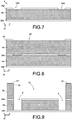
- Figures 7-12 describe steps for micromachining the second wafer 4.
- the first wafer 2 is arranged, including a substrate 31 of semiconductor material (e.g., silicon) having a front side 31a opposite to a back side 31b.
- a mask layer 17 is formed, made, for example, of TEOS oxide and having a thickness ranging between 0.5 ⁇ m and 2 ⁇ m, in particular 1 ⁇ m.
- the mask layer 17 is etched and partially removed so as to expose a surface portion of the substrate 31 of the wafer 2 where, in subsequent steps, the cavity 23 described with reference to Figure 1 will be formed.
- the structural layer 11 is, for example, grown epitaxially.
- the thickness of the structural layer 11 ranges between 2 ⁇ m and 50 ⁇ m.
- An insulation layer 25, Figure 4 is then formed, for example made of TEOS oxide and having a thickness ranging between 0.5 ⁇ m and 2 ⁇ m, in particular 1 ⁇ m, on the structural layer 11.
- the insulation layer 25 has the function of electrically insulating the wafer 2 from the piezoelectric actuator 3, manufactured in subsequent steps.
- Formation of the piezoelectric actuator 3 includes a step of formation, on the insulation layer 25, of the bottom electrode 19 (which is formed, for example, by a layer of TiO 2 having a thickness of between 5 nm and 50 nm on which a layer of Pt having a thickness ranging between 30 nm and 300 nm is deposited). This is then followed by deposition of a piezoelectric layer on the bottom electrode 19, via deposition of a layer of PZT (Pb, Zr, TiO 3 ), having a thickness ranging between 0.5 ⁇ m and 3.0 ⁇ m, more typically 1 ⁇ m or 2 ⁇ m (that will form, after subsequent definition steps, the piezoelectric region 16).
- deposited on the piezoelectric layer is a second layer of conductive material, for example Pt or Ir or IrO 2 or TiW or Ru, having a thickness ranging between 30 nm and 300 nm, to form the top electrode 18.
- the electrode and piezoelectric layers are subjected to lithographic and etching steps so as to pattern them according to a desired pattern, thus forming the bottom electrode 19, the piezoelectric region 16, and the top electrode 18.
- insulation and protection layers are then deposited on the bottom electrode 19, on the piezoelectric region 16, and on the top electrode 18.
- the insulation and protection layers include dielectric materials used for electrical insulation/passivation of the electrodes, for example, layers of USG, SiO 2 , or SiN, or Al 2 O 3 , either single or stacked, having a thickness ranging between 10 nm and 1000 nm.
- the embodiment illustrated includes sequential formation of a USG layer 21a, a SiN layer 21b and a dry-epoxy layer 21c, such as TMMR.
- the passivation layers are etched and selectively removed for creating trenches for access to the bottom electrode 19 and to the top electrode 18. This is followed by a step of deposition of conductive material within the trenches thus created, and a subsequent patterning step enables formation of conductive paths for selectively accessing the top electrode 18 and the bottom electrode 19 so as to electrically bias them during use. It is moreover possible to form further passivation layers to protect the conductive paths. Conductive pads are likewise formed alongside the piezoelectric actuator, electrically coupled to the conductive paths.
- the steps for manufacturing it envisage, Figure 7 , arranging the substrate 4a of semiconductor material (e.g., silicon) having a thickness ranging, for example, 400 ⁇ m, provided with mask layers 29a, 29b (made, for example, of TEOS, or SiO 2 , or SiN having a thickness of 1 ⁇ m) on both sides.
- the mask layer 29a is etched with masked etching so as to form openings 29a' that define regions of the second wafer 4, formed in which are the inlet holes 9, adapted to supply the fluid 6 to the chamber 10.
- the structural layer 4b formed on a top face of the second wafer 4, i.e., on the mask layer 29a, is the structural layer 4b, having a thickness ranging between 1 and 20 ⁇ m, for example, 4 ⁇ m.
- the structural layer 4b is, for example, formed by epitaxial growth.
- a step is carried out of formation of a further mask layer 35 (made, for example, of TEOS, or SiO 2 , or SiN having a thickness of 1 ⁇ m) on the structural layer 4b.
- the mask layer 35 is etched with masked etching so as to form an opening 35' that defines a region of the second wafer 4 in which, in subsequent steps, the chamber 10 will be formed.
- the opening 35' has an extension, in top plan view in the plane XY, such as to internally contain the openings 29a'. Moreover, as may be noted from Figure 10 , the opening 35' likewise has an extension, in top plan view in the plane XY, such as to internally contain both the piezoelectric actuator 3 and the outlet channel 33 of the first wafer 1, when the first and the second wafers 2, 4 are coupled together.
- FIG. 9 This is followed, Figure 9 , by a step of etching of the wafer 4 using the layers 29a, 29b, and 35 as etching masks. Selective portions of the substrate 4a and of the non-protected structural layer 4b are thus removed, to simultaneously form the inlet holes 9 and the chamber 10.
- a coupling layer 37 for example, of glue, is deposited on the mask layer 35.
- Machining steps are then carried out at the back side 31b of the substrate 31 of the first wafer 2.
- the substrate 31 is subjected to a step of chemical mechanical polishing (CMP) for reducing the thickness thereof. More in particular, the substrate 31 is completely removed.
- CMP chemical mechanical polishing
- the mask layer 17 is used for carrying out etching of the structural layer 11, which is removed throughout the entire thickness, where it is not protected by the mask layer 17, until the insulation layer 25 is reached and the cavity 23 is formed.
- the membrane 7, suspended over the cavity 23, is simultaneously formed.
- a step of coupling the nozzle plate 8 to the mask layer 17 is carried out, in particular by laminating a film of TMMF, which seals the cavity 23.
- the nozzle 13 is obtained by making a through-hole through the nozzle plate 8 in a region thereof such that, when coupled to the mask layer 17, it is vertically aligned (in the direction Z) with the outlet channel 33.
- a further step of selective etching of the portion of the mask layer 17 exposed through the nozzle 13 makes it possible to set the nozzle 13 in fluidic connection with the outlet channel 33.
- Figures 13-15 show the fluid ejection device 1 in operating steps, during use.
- the piezoelectric actuator 3 is controlled through the top electrode 18 and the bottom electrode 19 (appropriately biased) so as to generate a deflection of the membrane 7 towards the inside of the chamber 10. This deflection causes a movement of the fluid 6 through the channel 33, towards the nozzle 13, and generates controlled expulsion of a drop of fluid 6 towards the outside of the fluid ejection device 1.
- the piezoelectric actuator 3 is controlled through the top electrode 18 and the bottom electrode 19 so as to generate a deflection of the membrane 7 in a direction opposite to what is illustrated in Figure 14 , so as to increase the volume of the chamber 10, recalling further fluid 6 towards the chamber 10 through the inlet channels 9.
- the chamber 10 is hence recharged with fluid 6. It is thus possible to proceed cyclically by driving the piezoelectric actuator 3 for expulsion of further drops of fluid.
- the steps of Figures 14 and 15 are repeated throughout the entire printing process.
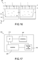
- Figure 16 is a schematic illustration of a printhead 100 comprising a plurality of ejection devices 1 formed as described previously and illustrated in Figure 16 only schematically and not in detail.
- the printhead 100 may be used not only for ink-jet printing, but also for applications such as high-precision deposition of liquid solutions containing, for example, organic material, or generally in the field of deposition techniques of an inkjet-printing type, for selective deposition of materials in the liquid phase.
- the printhead 100 further comprises a reservoir 101, arranged underneath the ejection devices 1, adapted to contain in an internal housing 102 of its own the fluid 6 (for example ink).
- a reservoir 101 arranged underneath the ejection devices 1, adapted to contain in an internal housing 102 of its own the fluid 6 (for example ink).
- FIG. 101 Further interfaces (e.g., a manifold) between the reservoir 101 and the ejection devices 1 may be present for fluidically coupling the reservoir 101 to the one or more inlet holes 9 of each ejection device 1.
- a manifold e.g., a manifold
- the printhead 100 may be incorporated in any printer of a known type, for example, of the type illustrated schematically in Figure 17 .
- the printer 200 of Figure 17 comprises a microprocessor 210, a memory 220 connected to the microprocessor 210, a printhead 100 including a plurality of ejection devices 1 according to the present invention (e.g., of the type shown in Figure 16 ), and a motor 230 for moving the printhead 100.
- the microprocessor 210 is connected to the printhead 100 and to the motor 230, and is configured to co-ordinate movement of the printhead 100 (obtained by running the motor 230) and ejection of the liquid (for example, ink) from the printhead 100.
- the operation of ejection of liquid is obtained by controlling operation of the piezoelectric actuator 3 of each ejection device 1, as illustrated in Figures 13-15 .
- the steps for manufacturing the fluid ejection device according to the present invention entail coupling of just two wafers, thus reducing the risks of misalignment, limiting the manufacturing costs, and rendering the final device structurally more solid.
Landscapes
- Engineering & Computer Science (AREA)
- Manufacturing & Machinery (AREA)
- Particle Formation And Scattering Control In Inkjet Printers (AREA)
- Reciprocating Pumps (AREA)
Abstract
Description
- The present invention relates to a method for manufacturing a fluid ejection device and to a fluid ejection device. In particular, the present invention relates a fluid ejection device, based upon piezoelectric technology, including just two wafers of semiconductor material machined and coupled together.
- Multiple types of fluid ejection devices are known in the prior art, in particular ink-jet heads for printing applications. Printheads of this sort, with appropriate modifications, can likewise be used for ejecting fluids other than ink, for example for applications in the biological or biomedical field, for local application of biological material (e.g., DNA) in the manufacture of sensors for biological analyses, for the decoration of fabrics or ceramics, and in applications of 3D printing and additive production.
- Known manufacturing methods envisage coupling via gluing or bonding of a large number of pre-machined components; typically, the various components are manufactured separately and assembled in a final production step. A printhead is typically formed by a large number of fluid ejection devices (of the order of hundreds or thousands), each of which includes a nozzle, a chamber for containing the fluid coupled to the nozzle, and an actuator coupled to the chamber, for causing outlet of the fluid through the respective nozzle. It is desirable for each of the fluid ejection devices belonging to a printhead to be as identical as possible to the other fluid ejection devices belonging to the same printhead, to guarantee uniformity of performance, above all in terms of volume of the fluid ejected and ejection rates.
- The method of assembly of the aforementioned pre-machined components proves costly and requires high precision; the resulting device moreover presents a large thickness.
- For instance, the patent document No.
US 2017/182778 discloses a method for manufacturing a fluid ejection device that envisages coupling of three wafers at least in part pre-machined. The method described envisages coupling steps (e.g., using bonding techniques) that require a high degree of accuracy in order to obtain a good alignment between the wafers and between the functional elements obtained therein. Moreover, formation of the actuation membrane of the ejection device (to which the piezoelectric actuator is coupled) envisages an etching step via which the area of the suspended portion of the membrane is defined. It is evident that devices manufactured at different times and/or with different machinery may be subject to undesired variations of the size of the aforesaid suspended area, with the risk of jeopardising reproducibility of the ejection device. - The aim of the present invention is to provide a method for manufacturing a fluid ejection device, and a fluid ejection device, that will overcome the drawbacks of the prior art.
- According to the present invention a method for manufacturing a fluid ejection device and a fluid ejection device are provided, as defined in the annexed claims.
- For a better understanding of the present invention, preferred embodiments thereof are now described, purely by way of non-limiting example, with reference to the attached drawings, wherein:
-
Figure 1 shows, in side cross-section view, a fluid ejection device obtained according to a method forming the subject of the present disclosure; -
Figures 2-12 show steps for manufacturing the fluid ejection device ofFigure 1 , according to an embodiment of the present invention; -
Figures 13-15 show the fluid ejection device manufactured according to the steps ofFigures 2-12 during respective operating steps; -
Figure 16 shows a printhead comprising the ejection device ofFigure 1 ; and -
Figure 17 shows a block diagram of a printer comprising the printhead ofFigure 16 . - With reference to
Figure 1 , afluid ejection device 1 is illustrated according to an aspect of the present disclosure.Figure 1 is a side cross-section view, taken along a plane XZ of a triaxial cartesian system X, Y, Z. - With reference to
Figure 1 , afirst wafer 2, including astructural layer 11 of semiconductor material, is machined so as to form thereon one or morepiezoelectric actuators 3, adapted to be controlled to generate a deflection of amembrane 7. Deflection of themembrane 7 causes a variation in the internal volume of one or morerespective chambers 10 adapted to define respective reservoirs for containing afluid 6 to be expelled during use through anoutlet channel 33.Figure 1 shows by way of example anindividual chamber 10 coupled to anindividual actuator 3. - A
second wafer 4 is machined so as to define the volume of thechamber 10 and so as to form one ormore inlet holes 9 for thefluid 6, in fluidic connection with thechambers 10.Figure 1 illustrates two inlet holes 9 (one of which can be used as recirculation channel). However, there may be present just oneinlet hole 9. - In the embodiment illustrated, the
second wafer 4 includes asubstrate 4a of semiconductor material, and astructural layer 4b of semiconductor material coupled to thesubstrate 4a. Theinlet holes 9 are formed through thesubstrate 4a, in particular throughout the thickness of thesubstrate 4a, whereas thestructural layer 4b is shaped so as to define the size and shape of thechamber 10. - One or more expulsion holes (nozzles) 13 for the
fluid 6 are formed in anozzle plate 8 separate from the first and thesecond wafers first wafer 2 at one side of the latter opposite to the side directly facing thesecond wafer 4. Thenozzle 13 is at least partially aligned, in the direction Z, to theoutlet channel 33, and, via the latter, is in fluidic connection with thechamber 10. - It may be noted that the
nozzle plate 8 is not a further wafer of semiconductor material, but a layer chosen from the following: a permanent epoxy-based dry-film photoresist, such as TMMF, or a dry-film based upon benzocyclobutene (BCB), or a dry-film of polydimethylsiloxane (PDMS). - In general, the
nozzle plate 8 is chosen from a material such as to guarantee chemical stability to acid or alkaline solutions, organic solvents and other compounds that could be present in thefluid 6 to be ejected. The present applicant has found that TMMF is adapted to various microfluidic applications. - The
nozzle plate 8 has a thickness, measured along Z, of between 5 µm and 100 µm, for example 50 µm. - The first and the
second wafers references 35, 37 (see alsoFigure 9 ). In particular, the first and thesecond wafers piezoelectric actuator 3 extends towards thechamber 10. - Extending between the
nozzle plate 8 and thefirst wafer 2, in particular between thenozzle plate 8 and themembrane 7, is acavity 23 having a shape and dimensions such as to enable deflection of themembrane 7 towards thenozzle plate 8. - The
piezoelectric actuator 3 comprises apiezoelectric region 16 arranged between atop electrode 18 and abottom electrode 19, adapted to supply an electrical signal to thepiezoelectric region 16 for generating, in use, a deflection of thepiezoelectric region 16, which, consequently, causes a deflection of themembrane 7, in a way in itself known. Metal paths (not illustrated inFigure 1 ) extend from thetop electrode 18 and from thebottom electrode 19 towards an electrical contact region, provided with contact pads (also not illustrated) adapted to be biased during use, to activate theactuator 3. - Since the
piezoelectric actuator 3 faces thechamber 10, one or more insulation and protection layers cover thepiezoelectric actuator 3. In the embodiment illustrated, the insulation and protection layers comprise: afirst passivation layer 21a (made, for example, of undoped silica glass (USG), or SiO2, or SiN, or some other dielectric material), which extends over thepiezoelectric region 16 and over thetop electrode 18 andbottom electrode 19, to cover theregion 16 completely; asecond passivation layer 21b (made, for example, of silicon nitride), which extends over thefirst passivation layer 21a to completely cover the latter; and aprotection layer 21c, which extends over thesecond passivation layer 21b to completely cover the latter. - The
protection layer 21c is, for example, a dry-epoxy layer (epoxy-based dry-film), of commercially available type, such as TMMR or BCB. Theprotection layer 21c has the function of protecting the piezoelectric actuator and theunderlying passivation layers fluid 6 that, in use, is present in thechamber 10. - The
first passivation layer 21a has a thickness ranging between 0.1 µm and 0.5 µm and has the function of intermetal insulating dielectric. Thesecond passivation layer 21b has a thickness ranging between 2 µm and 10 µm and has the function of passivation. Theprotection layer 21c has a thickness ranging between 2 µm and 10 µm and has the function of chemical barrier against the fluid to be ejected. - With reference to
Figures 2-12 , a method is now described for manufacturing thefluid ejection device 1 according to an embodiment of the present invention. - In particular,
Figures 2-6 describe steps for micromachining thefirst wafer 2, andFigures 7-12 describe steps for micromachining thesecond wafer 4. - With reference to
Figure 2 , thefirst wafer 2 is arranged, including asubstrate 31 of semiconductor material (e.g., silicon) having afront side 31a opposite to aback side 31b. Next, on thefront side 31a of the aforesaid substrate amask layer 17 is formed, made, for example, of TEOS oxide and having a thickness ranging between 0.5 µm and 2 µm, in particular 1 µm. Themask layer 17 is etched and partially removed so as to expose a surface portion of thesubstrate 31 of thewafer 2 where, in subsequent steps, thecavity 23 described with reference toFigure 1 will be formed. - This is followed,
Figure 2 , by a step of formation of thestructural layer 11 on thefront side 31a of thesubstrate 31 and of the portions of themask layer 17 not removed during the previous etching step. Thestructural layer 11 is, for example, grown epitaxially. The thickness of thestructural layer 11 ranges between 2 µm and 50 µm. - An
insulation layer 25,Figure 4 , is then formed, for example made of TEOS oxide and having a thickness ranging between 0.5 µm and 2 µm, in particular 1 µm, on thestructural layer 11. Theinsulation layer 25 has the function of electrically insulating thewafer 2 from thepiezoelectric actuator 3, manufactured in subsequent steps. - Formation of the
piezoelectric actuator 3 includes a step of formation, on theinsulation layer 25, of the bottom electrode 19 (which is formed, for example, by a layer of TiO2 having a thickness of between 5 nm and 50 nm on which a layer of Pt having a thickness ranging between 30 nm and 300 nm is deposited). This is then followed by deposition of a piezoelectric layer on thebottom electrode 19, via deposition of a layer of PZT (Pb, Zr, TiO3), having a thickness ranging between 0.5 µm and 3.0 µm, more typically 1 µm or 2 µm (that will form, after subsequent definition steps, the piezoelectric region 16). Next, deposited on the piezoelectric layer is a second layer of conductive material, for example Pt or Ir or IrO2 or TiW or Ru, having a thickness ranging between 30 nm and 300 nm, to form thetop electrode 18. - The electrode and piezoelectric layers are subjected to lithographic and etching steps so as to pattern them according to a desired pattern, thus forming the
bottom electrode 19, thepiezoelectric region 16, and thetop electrode 18. - One or more insulation and protection layers are then deposited on the
bottom electrode 19, on thepiezoelectric region 16, and on thetop electrode 18. The insulation and protection layers include dielectric materials used for electrical insulation/passivation of the electrodes, for example, layers of USG, SiO2, or SiN, or Al2O3, either single or stacked, having a thickness ranging between 10 nm and 1000 nm. - As described previously, the embodiment illustrated includes sequential formation of a
USG layer 21a, aSiN layer 21b and a dry-epoxy layer 21c, such as TMMR. - In a way not illustrated in the figures, in so far as it does not form part of the present disclosure, and is in itself known, for example, from
US 2017/182778 , the passivation layers are etched and selectively removed for creating trenches for access to thebottom electrode 19 and to thetop electrode 18. This is followed by a step of deposition of conductive material within the trenches thus created, and a subsequent patterning step enables formation of conductive paths for selectively accessing thetop electrode 18 and thebottom electrode 19 so as to electrically bias them during use. It is moreover possible to form further passivation layers to protect the conductive paths. Conductive pads are likewise formed alongside the piezoelectric actuator, electrically coupled to the conductive paths. - This is followed,
Figure 6 , by steps of masked etching of the insulation andprotection layers 21a-21c, of theinsulation layer 25, and of thestructural layer 11, until themask layer 17 is reached. This etch is carried out alongside thepiezoelectric actuator 3, using a mask shaped so as to expose a region having, in top plan view in the plane XY, a substantially circular shape with a diameter ranging between 10 µm and 200 µm. There is thus formed anoutlet channel 33 through part of thefirst wafer 2; as illustrated in subsequent steps, theoutlet channel 33 forms part of a fluidic connection between thechamber 10 and thenozzle 13, for passage of thefluid 6 to be ejected through thenozzle 13. - With reference to the
second wafer 4, the steps for manufacturing it envisage,Figure 7 , arranging thesubstrate 4a of semiconductor material (e.g., silicon) having a thickness ranging, for example, 400 µm, provided withmask layers mask layer 29a is etched with masked etching so as to formopenings 29a' that define regions of thesecond wafer 4, formed in which are the inlet holes 9, adapted to supply thefluid 6 to thechamber 10. - With reference to
Figure 8 , formed on a top face of thesecond wafer 4, i.e., on themask layer 29a, is thestructural layer 4b, having a thickness ranging between 1 and 20 µm, for example, 4 µm. Thestructural layer 4b is, for example, formed by epitaxial growth. Then a step is carried out of formation of a further mask layer 35 (made, for example, of TEOS, or SiO2, or SiN having a thickness of 1 µm) on thestructural layer 4b. Themask layer 35 is etched with masked etching so as to form an opening 35' that defines a region of thesecond wafer 4 in which, in subsequent steps, thechamber 10 will be formed. For this purpose, the opening 35' has an extension, in top plan view in the plane XY, such as to internally contain theopenings 29a'. Moreover, as may be noted fromFigure 10 , the opening 35' likewise has an extension, in top plan view in the plane XY, such as to internally contain both thepiezoelectric actuator 3 and theoutlet channel 33 of thefirst wafer 1, when the first and thesecond wafers - This is followed,
Figure 9 , by a step of etching of thewafer 4 using thelayers substrate 4a and of the non-protectedstructural layer 4b are thus removed, to simultaneously form the inlet holes 9 and thechamber 10. Acoupling layer 37, for example, of glue, is deposited on themask layer 35. - This is then followed,
Figure 10 , by a step of coupling between the first and thesecond wafers mask layer 35 to theprotection layer 21c of thefirst wafer 2, via thecoupling layer 37. More in particular, coupling between thewafers chamber 10 completely houses thepiezoelectric actuator 3 and so that theoutlet channel 33 is in fluidic connection with theinlet hole 9 via thechamber 10. There is thus obtained a stack of the twowafers - Machining steps are then carried out at the
back side 31b of thesubstrate 31 of thefirst wafer 2. In particular,Figure 11 , thesubstrate 31 is subjected to a step of chemical mechanical polishing (CMP) for reducing the thickness thereof. More in particular, thesubstrate 31 is completely removed. - Then,
Figure 12 , themask layer 17 is used for carrying out etching of thestructural layer 11, which is removed throughout the entire thickness, where it is not protected by themask layer 17, until theinsulation layer 25 is reached and thecavity 23 is formed. Themembrane 7, suspended over thecavity 23, is simultaneously formed. - Finally, a step of coupling the
nozzle plate 8 to themask layer 17 is carried out, in particular by laminating a film of TMMF, which seals thecavity 23. In a step prior or subsequent to coupling of thenozzle plate 8 to themask layer 17, thenozzle 13 is obtained by making a through-hole through thenozzle plate 8 in a region thereof such that, when coupled to themask layer 17, it is vertically aligned (in the direction Z) with theoutlet channel 33. A further step of selective etching of the portion of themask layer 17 exposed through thenozzle 13 makes it possible to set thenozzle 13 in fluidic connection with theoutlet channel 33. - Alternatively to what has been described above, it is likewise possible, using a mask obtained for this purpose, to etch the portion of the
mask layer 17 at thechannel 33 prior to the step of coupling thenozzle plate 8 to themask layer 17. - The
ejection device 1 ofFigure 1 is thus obtained. -
Figures 13-15 show thefluid ejection device 1 in operating steps, during use. - In a first step,
Figure 13 , thechamber 10 is filled with thefluid 6 is to be ejected. This step of loading of thefluid 6 is carried out through theinlet channels 9. - Then,
Figure 14 , thepiezoelectric actuator 3 is controlled through thetop electrode 18 and the bottom electrode 19 (appropriately biased) so as to generate a deflection of themembrane 7 towards the inside of thechamber 10. This deflection causes a movement of thefluid 6 through thechannel 33, towards thenozzle 13, and generates controlled expulsion of a drop offluid 6 towards the outside of thefluid ejection device 1. - Next,
Figure 15 , thepiezoelectric actuator 3 is controlled through thetop electrode 18 and thebottom electrode 19 so as to generate a deflection of themembrane 7 in a direction opposite to what is illustrated inFigure 14 , so as to increase the volume of thechamber 10, recallingfurther fluid 6 towards thechamber 10 through theinlet channels 9. Thechamber 10 is hence recharged withfluid 6. It is thus possible to proceed cyclically by driving thepiezoelectric actuator 3 for expulsion of further drops of fluid. The steps ofFigures 14 and 15 are repeated throughout the entire printing process. - Driving of the piezoelectric element by biasing of the top and
bottom electrodes -
Figure 16 is a schematic illustration of aprinthead 100 comprising a plurality ofejection devices 1 formed as described previously and illustrated inFigure 16 only schematically and not in detail. - The
printhead 100 may be used not only for ink-jet printing, but also for applications such as high-precision deposition of liquid solutions containing, for example, organic material, or generally in the field of deposition techniques of an inkjet-printing type, for selective deposition of materials in the liquid phase. - The
printhead 100 further comprises areservoir 101, arranged underneath theejection devices 1, adapted to contain in aninternal housing 102 of its own the fluid 6 (for example ink). - Further interfaces (e.g., a manifold) between the
reservoir 101 and theejection devices 1 may be present for fluidically coupling thereservoir 101 to the one ormore inlet holes 9 of eachejection device 1. - The
printhead 100 may be incorporated in any printer of a known type, for example, of the type illustrated schematically inFigure 17 . - The
printer 200 ofFigure 17 comprises amicroprocessor 210, a memory 220 connected to themicroprocessor 210, aprinthead 100 including a plurality ofejection devices 1 according to the present invention (e.g., of the type shown inFigure 16 ), and amotor 230 for moving theprinthead 100. Themicroprocessor 210 is connected to theprinthead 100 and to themotor 230, and is configured to co-ordinate movement of the printhead 100 (obtained by running the motor 230) and ejection of the liquid (for example, ink) from theprinthead 100. The operation of ejection of liquid is obtained by controlling operation of thepiezoelectric actuator 3 of eachejection device 1, as illustrated inFigures 13-15 . - From an examination of the characteristics of the present invention, according to the present disclosure, the advantages that it affords are evident.
- In particular, it may be noted that the steps for manufacturing the fluid ejection device according to the present invention entail coupling of just two wafers, thus reducing the risks of misalignment, limiting the manufacturing costs, and rendering the final device structurally more solid.
- In fact, an error committed during the steps of gluing of a number of wafers is difficult to recover, and there may be noted an effect of error accumulation in the formation of a stack of wafers, which rapidly leads to a final device does not function properly. Moreover, it may be noted that mechanical bonding, normally used for coupling wafers, enables a precision of alignment of some micrometres to be achieved, typically more than 5 µm; instead, machining steps that envisage photolithographic steps enable a level of precision of below 0.5 µm to be achieved and are consequently advantageous.
- Finally, it is clear that modifications and variations may be made to what has been described and illustrated herein, without thereby departing from the scope of the present invention, as defined in the annexed claims.
Claims (11)
- A method for manufacturing a device (1) for ejecting a fluid (6), comprising the steps of:forming, at a first side of a first wafer (2) of semiconductor material, a piezoelectric actuator (3) and an outlet channel (33) for said fluid (6) laterally to the piezoelectric actuator (3);forming, at a first side of a second wafer (4) of semiconductor material, a recess (10) and forming, at a second side of the second wafer (4) opposite to the first side of the second wafer (4), at least one inlet channel (9) for said fluid (6) fluidically coupled to the recess (10);coupling the first and the second wafers (2, 4) together so that the piezoelectric actuator (3) and the outlet channel (33) directly face, and are completely contained in, the recess (10), said recess (10) forming a reservoir of said fluid (6) within the fluid ejection device (1);coupling a dry-film (8) at a second side, opposite to the first side, of the first wafer (2); andforming an ejection nozzle (13), at least partially aligned to the outlet channel (33), through said dry-film (8), so that the ejection nozzle (13) is in fluidic connection with said reservoir (10) through said outlet channel (33).
- The method according to Claim 1, further comprising the step of forming a multilayer stack (21a-21c) on the piezoelectric actuator (3) and laterally to the piezoelectric actuator (3), for insulating and protecting the piezoelectric actuator from a contact with said fluid (6),
wherein the step of coupling the first and the second wafers (2, 4) together includes gluing the second wafer at portions of the multilayer stack (21a-21c), that extend laterally to the piezoelectric actuator (3). - The method according to Claim 2, wherein the step of forming the outlet channel (33) comprises removing selective portions of the multilayer stack (21a-21c) laterally to the piezoelectric actuator (3).
- The method according to any one of the preceding claims, further comprising the steps of:providing the first wafer (2) including a semiconductor multilayer (31);forming on the substrate (31), on the second side of the first wafer (2), a hard mask (17) shaped so as to have an opening, through which said substrate (31) is exposed;forming, on the hard mask (17) and in said opening of the hard mask (17), a structural layer (11);forming, on the structural layer (11), an electrical-insulation layer (25);forming, on the electrical-insulation layer (25), at said opening of the hard mask (17), said piezoelectric actuator (3);removing said substrate (31) until said hard mask (17) is reached;removing selective portions of the structural layer (11) exposed through the opening of the hard mask (17) until said insulating layer (25) is reached, thus forming a membrane (17) that can be controlled in deflection by means of said piezoelectric actuator.
- The method according to any one of the preceding claims, wherein the step of coupling said dry-film comprises laminating a permanent epoxy-based dry-film photoresist.
- An ejection device (1) for a fluid (6), comprising:a first solid body (2), housing, on a first side thereof, a piezoelectric actuator (3) and an outlet channel (33) for said fluid (6) alongside the piezoelectric actuator (3) ;a second solid body (4) having, on a first side thereof, a recess (10) and, on a second side thereof opposite to the first side, at least one inlet channel (9) for inlet of said fluid (6) fluidically coupled to the recess (10); anda dry-film (8) coupled to a second side, opposite to the first side, of the first solid body (2),wherein the first and the second solid bodies (2, 4) are coupled together so that the piezoelectric actuator (3) and the outlet channel (33) are directly facing, and completely contained in, the recess (10), said recess (10) forming a reservoir of said fluid (6) within the fluid ejection device (1);and wherein the dry-film (8) has a through hole forming an ejection nozzle (13) of said ejection device (1), which extends at least partially aligned to the outlet channel (33) so that the ejection nozzle (13) is in fluidic connection with said reservoir (10) through said outlet channel (33).
- The ejection device according to Claim 1, further comprising a multilayer stack (21a-21c), which extends over the piezoelectric actuator (3) and alongside the piezoelectric actuator (3), to cover the piezoelectric actuator (3) completely in order to insulate and protect the piezoelectric actuator from a contact with said fluid (6),
wherein the second solid body (4) is glued to the first solid body (2) at portions of the multilayer stack (21a-21c) that extend alongside the piezoelectric actuator (3). - The ejection device according to Claim 6 or 7, wherein the first solid body (2) further comprises a membrane (7),
said piezoelectric actuator (3) being mechanically coupled to said membrane (7) to cause a deflection thereof, when it is activated. - The ejection device according to any one of the Claims 6 to 8, wherein said dry-film (8) is a permanent epoxy-based dry-film photoresist.
- A printhead (100) comprising a plurality of fluid ejection devices according to any one of the Claims 6 to 9.
- A printer (200) comprising at least one printhead (100) according to Claim 10.
Applications Claiming Priority (1)
| Application Number | Priority Date | Filing Date | Title |
|---|---|---|---|
| IT102019000005794A IT201900005794A1 (en) | 2019-04-15 | 2019-04-15 | FLUID EJECTION DEVICE WITH REDUCED NUMBER OF COMPONENTS AND MANUFACTURING METHOD OF THE FLUID EJECTION DEVICE |
Publications (2)
| Publication Number | Publication Date |
|---|---|
| EP3725531A1 true EP3725531A1 (en) | 2020-10-21 |
| EP3725531B1 EP3725531B1 (en) | 2023-05-31 |
Family
ID=67185671
Family Applications (1)
| Application Number | Title | Priority Date | Filing Date |
|---|---|---|---|
| EP20169708.3A Active EP3725531B1 (en) | 2019-04-15 | 2020-04-15 | Fluid ejection device with reduced number of components, and method for manufacturing the fluid ejection device |
Country Status (4)
| Country | Link |
|---|---|
| US (2) | US11260659B2 (en) |
| EP (1) | EP3725531B1 (en) |
| CN (2) | CN111823717B (en) |
| IT (1) | IT201900005794A1 (en) |
Families Citing this family (3)
| Publication number | Priority date | Publication date | Assignee | Title |
|---|---|---|---|---|
| IT201900005794A1 (en) * | 2019-04-15 | 2020-10-15 | St Microelectronics Srl | FLUID EJECTION DEVICE WITH REDUCED NUMBER OF COMPONENTS AND MANUFACTURING METHOD OF THE FLUID EJECTION DEVICE |
| JP7725911B2 (en) * | 2021-07-26 | 2025-08-20 | 株式会社リコー | Actuator, liquid ejection head, liquid ejection unit, and liquid ejection device |
| US20230110175A1 (en) | 2021-09-29 | 2023-04-13 | Stmicroelectronics S.R.L. | Microfluidic mems device comprising a buried chamber and manufacturing process thereof |
Citations (4)
| Publication number | Priority date | Publication date | Assignee | Title |
|---|---|---|---|---|
| EP1089360A1 (en) * | 1999-04-06 | 2001-04-04 | Matsushita Electric Industrial Co., Ltd. | Piezoelectric thin film device, inkjet recording head using the device and manufacturing methods of the device and the head |
| US20170182778A1 (en) | 2015-12-29 | 2017-06-29 | Stmicroelectronics S.R.L. | Manufacturing method for a fluid-ejection device, and fluid-ejection device |
| US20180154635A1 (en) * | 2016-12-06 | 2018-06-07 | Canon Kabushiki Kaisha | Liquid ejection head |
| EP3431295A1 (en) * | 2017-07-20 | 2019-01-23 | STMicroelectronics S.r.l. | Microfluidic mems device for inkjet printing with piezoelectric actuation and manufacturing process thereof |
Family Cites Families (7)
| Publication number | Priority date | Publication date | Assignee | Title |
|---|---|---|---|---|
| JP4984018B2 (en) | 2005-03-30 | 2012-07-25 | セイコーエプソン株式会社 | Piezoelectric element, liquid ejecting head, and liquid ejecting apparatus |
| JP5453960B2 (en) | 2008-09-19 | 2014-03-26 | セイコーエプソン株式会社 | Liquid ejecting head, liquid ejecting apparatus, and actuator device |
| EP2726294B1 (en) | 2011-06-29 | 2018-10-17 | Hewlett-Packard Development Company, L.P. | Piezoelectric inkjet die stack |
| JP6201584B2 (en) | 2013-09-30 | 2017-09-27 | ブラザー工業株式会社 | Droplet ejector and method for manufacturing droplet ejector |
| US10022957B2 (en) * | 2015-04-24 | 2018-07-17 | Fujifilm Dimatrix, Inc. | Fluid ejection devices with reduced crosstalk |
| IT201700034134A1 (en) * | 2017-03-28 | 2018-09-28 | St Microelectronics Srl | FLUID-RELEASE DEVICE WITH CROSSTALK REDUCTION ELEMENT, PRINT HEAD INCLUDING THE EJECTION DEVICE, PRINTER INCLUDING THE PRINT HEAD AND PROCESS OF MANUFACTURING THE EJECTION DEVICE |
| IT201900005794A1 (en) | 2019-04-15 | 2020-10-15 | St Microelectronics Srl | FLUID EJECTION DEVICE WITH REDUCED NUMBER OF COMPONENTS AND MANUFACTURING METHOD OF THE FLUID EJECTION DEVICE |
-
2019
- 2019-04-15 IT IT102019000005794A patent/IT201900005794A1/en unknown
-
2020
- 2020-04-14 CN CN202010289274.2A patent/CN111823717B/en active Active
- 2020-04-14 CN CN202020542341.2U patent/CN212499504U/en active Active
- 2020-04-14 US US16/848,549 patent/US11260659B2/en active Active
- 2020-04-15 EP EP20169708.3A patent/EP3725531B1/en active Active
-
2022
- 2022-01-10 US US17/572,374 patent/US11884071B2/en active Active
Patent Citations (4)
| Publication number | Priority date | Publication date | Assignee | Title |
|---|---|---|---|---|
| EP1089360A1 (en) * | 1999-04-06 | 2001-04-04 | Matsushita Electric Industrial Co., Ltd. | Piezoelectric thin film device, inkjet recording head using the device and manufacturing methods of the device and the head |
| US20170182778A1 (en) | 2015-12-29 | 2017-06-29 | Stmicroelectronics S.R.L. | Manufacturing method for a fluid-ejection device, and fluid-ejection device |
| US20180154635A1 (en) * | 2016-12-06 | 2018-06-07 | Canon Kabushiki Kaisha | Liquid ejection head |
| EP3431295A1 (en) * | 2017-07-20 | 2019-01-23 | STMicroelectronics S.r.l. | Microfluidic mems device for inkjet printing with piezoelectric actuation and manufacturing process thereof |
Also Published As
| Publication number | Publication date |
|---|---|
| CN111823717B (en) | 2023-08-29 |
| US11884071B2 (en) | 2024-01-30 |
| EP3725531B1 (en) | 2023-05-31 |
| US20220126580A1 (en) | 2022-04-28 |
| CN212499504U (en) | 2021-02-09 |
| US20200324545A1 (en) | 2020-10-15 |
| IT201900005794A1 (en) | 2020-10-15 |
| CN111823717A (en) | 2020-10-27 |
| US11260659B2 (en) | 2022-03-01 |
Similar Documents
| Publication | Publication Date | Title |
|---|---|---|
| EP3173235B1 (en) | Fluid ejection device with restriction channel, and manufacturing method thereof | |
| US10245834B2 (en) | Manufacturing method for a fluid-ejection device, and fluid-ejection device | |
| US8998388B2 (en) | Method for manufacturing a fluid ejection device and fluid ejection device | |
| US11214061B2 (en) | Microfluidic MEMS device with piezoelectric actuation and manufacturing process thereof | |
| CN108656747B (en) | Fluid ejection device, printhead, printer, and method for making an ejection device | |
| US11884071B2 (en) | Fluid ejection device with reduced number of components, and method for manufacturing the fluid ejection device | |
| US11498335B2 (en) | Method for manufacturing a fluid-ejection device with improved resonance frequency and fluid ejection velocity, and fluid-ejection device | |
| US20060181581A1 (en) | Piezoelectric inkjet printhead and method of manufacturing the same | |
| US20090212008A1 (en) | Liquid ejection head and manufacturing method thereof | |
| US20130083126A1 (en) | Liquid ejection device with planarized nozzle plate | |
| EP1681169B1 (en) | Piezoelectric inkjet printhead and method of manufacturing the same | |
| US8037605B2 (en) | Piezoelectric inkjet printhead and method of manufacturing the same | |
| US20070220723A1 (en) | Method for manufacturing inkjet head | |
| EP4108462B1 (en) | Improved microfluidic device for spraying very small drops of liquids | |
| US20130082028A1 (en) | Forming a planar film over microfluidic device openings | |
| KR20040073120A (en) | Manufacturing method of piezoelectric ink-jet printhead |
Legal Events
| Date | Code | Title | Description |
|---|---|---|---|
| PUAI | Public reference made under article 153(3) epc to a published international application that has entered the european phase |
Free format text: ORIGINAL CODE: 0009012 |
|
| STAA | Information on the status of an ep patent application or granted ep patent |
Free format text: STATUS: THE APPLICATION HAS BEEN PUBLISHED |
|
| AK | Designated contracting states |
Kind code of ref document: A1 Designated state(s): AL AT BE BG CH CY CZ DE DK EE ES FI FR GB GR HR HU IE IS IT LI LT LU LV MC MK MT NL NO PL PT RO RS SE SI SK SM TR |
|
| AX | Request for extension of the european patent |
Extension state: BA ME |
|
| STAA | Information on the status of an ep patent application or granted ep patent |
Free format text: STATUS: REQUEST FOR EXAMINATION WAS MADE |
|
| 17P | Request for examination filed |
Effective date: 20210225 |
|
| RBV | Designated contracting states (corrected) |
Designated state(s): AL AT BE BG CH CY CZ DE DK EE ES FI FR GB GR HR HU IE IS IT LI LT LU LV MC MK MT NL NO PL PT RO RS SE SI SK SM TR |
|
| GRAP | Despatch of communication of intention to grant a patent |
Free format text: ORIGINAL CODE: EPIDOSNIGR1 |
|
| STAA | Information on the status of an ep patent application or granted ep patent |
Free format text: STATUS: GRANT OF PATENT IS INTENDED |
|
| RIC1 | Information provided on ipc code assigned before grant |
Ipc: B41J 2/16 20060101ALI20221018BHEP Ipc: B41J 2/14 20060101AFI20221018BHEP |
|
| INTG | Intention to grant announced |
Effective date: 20221111 |
|
| GRAS | Grant fee paid |
Free format text: ORIGINAL CODE: EPIDOSNIGR3 |
|
| GRAA | (expected) grant |
Free format text: ORIGINAL CODE: 0009210 |
|
| STAA | Information on the status of an ep patent application or granted ep patent |
Free format text: STATUS: THE PATENT HAS BEEN GRANTED |
|
| AK | Designated contracting states |
Kind code of ref document: B1 Designated state(s): AL AT BE BG CH CY CZ DE DK EE ES FI FR GB GR HR HU IE IS IT LI LT LU LV MC MK MT NL NO PL PT RO RS SE SI SK SM TR |
|
| REG | Reference to a national code |
Ref country code: GB Ref legal event code: FG4D Ref country code: CH Ref legal event code: EP |
|
| REG | Reference to a national code |
Ref country code: AT Ref legal event code: REF Ref document number: 1570719 Country of ref document: AT Kind code of ref document: T Effective date: 20230615 Ref country code: DE Ref legal event code: R096 Ref document number: 602020011239 Country of ref document: DE |
|
| REG | Reference to a national code |
Ref country code: IE Ref legal event code: FG4D |
|
| REG | Reference to a national code |
Ref country code: LT Ref legal event code: MG9D |
|
| REG | Reference to a national code |
Ref country code: NL Ref legal event code: MP Effective date: 20230531 |
|
| REG | Reference to a national code |
Ref country code: AT Ref legal event code: MK05 Ref document number: 1570719 Country of ref document: AT Kind code of ref document: T Effective date: 20230531 |
|
| PG25 | Lapsed in a contracting state [announced via postgrant information from national office to epo] |
Ref country code: SE Free format text: LAPSE BECAUSE OF FAILURE TO SUBMIT A TRANSLATION OF THE DESCRIPTION OR TO PAY THE FEE WITHIN THE PRESCRIBED TIME-LIMIT Effective date: 20230531 Ref country code: NO Free format text: LAPSE BECAUSE OF FAILURE TO SUBMIT A TRANSLATION OF THE DESCRIPTION OR TO PAY THE FEE WITHIN THE PRESCRIBED TIME-LIMIT Effective date: 20230831 Ref country code: ES Free format text: LAPSE BECAUSE OF FAILURE TO SUBMIT A TRANSLATION OF THE DESCRIPTION OR TO PAY THE FEE WITHIN THE PRESCRIBED TIME-LIMIT Effective date: 20230531 Ref country code: AT Free format text: LAPSE BECAUSE OF FAILURE TO SUBMIT A TRANSLATION OF THE DESCRIPTION OR TO PAY THE FEE WITHIN THE PRESCRIBED TIME-LIMIT Effective date: 20230531 |
|
| PG25 | Lapsed in a contracting state [announced via postgrant information from national office to epo] |
Ref country code: RS Free format text: LAPSE BECAUSE OF FAILURE TO SUBMIT A TRANSLATION OF THE DESCRIPTION OR TO PAY THE FEE WITHIN THE PRESCRIBED TIME-LIMIT Effective date: 20230531 Ref country code: PL Free format text: LAPSE BECAUSE OF FAILURE TO SUBMIT A TRANSLATION OF THE DESCRIPTION OR TO PAY THE FEE WITHIN THE PRESCRIBED TIME-LIMIT Effective date: 20230531 Ref country code: NL Free format text: LAPSE BECAUSE OF FAILURE TO SUBMIT A TRANSLATION OF THE DESCRIPTION OR TO PAY THE FEE WITHIN THE PRESCRIBED TIME-LIMIT Effective date: 20230531 Ref country code: LV Free format text: LAPSE BECAUSE OF FAILURE TO SUBMIT A TRANSLATION OF THE DESCRIPTION OR TO PAY THE FEE WITHIN THE PRESCRIBED TIME-LIMIT Effective date: 20230531 Ref country code: LT Free format text: LAPSE BECAUSE OF FAILURE TO SUBMIT A TRANSLATION OF THE DESCRIPTION OR TO PAY THE FEE WITHIN THE PRESCRIBED TIME-LIMIT Effective date: 20230531 Ref country code: IS Free format text: LAPSE BECAUSE OF FAILURE TO SUBMIT A TRANSLATION OF THE DESCRIPTION OR TO PAY THE FEE WITHIN THE PRESCRIBED TIME-LIMIT Effective date: 20230930 Ref country code: HR Free format text: LAPSE BECAUSE OF FAILURE TO SUBMIT A TRANSLATION OF THE DESCRIPTION OR TO PAY THE FEE WITHIN THE PRESCRIBED TIME-LIMIT Effective date: 20230531 Ref country code: GR Free format text: LAPSE BECAUSE OF FAILURE TO SUBMIT A TRANSLATION OF THE DESCRIPTION OR TO PAY THE FEE WITHIN THE PRESCRIBED TIME-LIMIT Effective date: 20230901 |
|
| PG25 | Lapsed in a contracting state [announced via postgrant information from national office to epo] |
Ref country code: FI Free format text: LAPSE BECAUSE OF FAILURE TO SUBMIT A TRANSLATION OF THE DESCRIPTION OR TO PAY THE FEE WITHIN THE PRESCRIBED TIME-LIMIT Effective date: 20230531 |
|
| PG25 | Lapsed in a contracting state [announced via postgrant information from national office to epo] |
Ref country code: SK Free format text: LAPSE BECAUSE OF FAILURE TO SUBMIT A TRANSLATION OF THE DESCRIPTION OR TO PAY THE FEE WITHIN THE PRESCRIBED TIME-LIMIT Effective date: 20230531 |
|
| PG25 | Lapsed in a contracting state [announced via postgrant information from national office to epo] |
Ref country code: SM Free format text: LAPSE BECAUSE OF FAILURE TO SUBMIT A TRANSLATION OF THE DESCRIPTION OR TO PAY THE FEE WITHIN THE PRESCRIBED TIME-LIMIT Effective date: 20230531 Ref country code: SK Free format text: LAPSE BECAUSE OF FAILURE TO SUBMIT A TRANSLATION OF THE DESCRIPTION OR TO PAY THE FEE WITHIN THE PRESCRIBED TIME-LIMIT Effective date: 20230531 Ref country code: RO Free format text: LAPSE BECAUSE OF FAILURE TO SUBMIT A TRANSLATION OF THE DESCRIPTION OR TO PAY THE FEE WITHIN THE PRESCRIBED TIME-LIMIT Effective date: 20230531 Ref country code: PT Free format text: LAPSE BECAUSE OF FAILURE TO SUBMIT A TRANSLATION OF THE DESCRIPTION OR TO PAY THE FEE WITHIN THE PRESCRIBED TIME-LIMIT Effective date: 20231002 Ref country code: EE Free format text: LAPSE BECAUSE OF FAILURE TO SUBMIT A TRANSLATION OF THE DESCRIPTION OR TO PAY THE FEE WITHIN THE PRESCRIBED TIME-LIMIT Effective date: 20230531 Ref country code: DK Free format text: LAPSE BECAUSE OF FAILURE TO SUBMIT A TRANSLATION OF THE DESCRIPTION OR TO PAY THE FEE WITHIN THE PRESCRIBED TIME-LIMIT Effective date: 20230531 Ref country code: CZ Free format text: LAPSE BECAUSE OF FAILURE TO SUBMIT A TRANSLATION OF THE DESCRIPTION OR TO PAY THE FEE WITHIN THE PRESCRIBED TIME-LIMIT Effective date: 20230531 |
|
| REG | Reference to a national code |
Ref country code: DE Ref legal event code: R097 Ref document number: 602020011239 Country of ref document: DE |
|
| PLBE | No opposition filed within time limit |
Free format text: ORIGINAL CODE: 0009261 |
|
| STAA | Information on the status of an ep patent application or granted ep patent |
Free format text: STATUS: NO OPPOSITION FILED WITHIN TIME LIMIT |
|
| PG25 | Lapsed in a contracting state [announced via postgrant information from national office to epo] |
Ref country code: SI Free format text: LAPSE BECAUSE OF FAILURE TO SUBMIT A TRANSLATION OF THE DESCRIPTION OR TO PAY THE FEE WITHIN THE PRESCRIBED TIME-LIMIT Effective date: 20230531 |
|
| 26N | No opposition filed |
Effective date: 20240301 |
|
| PG25 | Lapsed in a contracting state [announced via postgrant information from national office to epo] |
Ref country code: SI Free format text: LAPSE BECAUSE OF FAILURE TO SUBMIT A TRANSLATION OF THE DESCRIPTION OR TO PAY THE FEE WITHIN THE PRESCRIBED TIME-LIMIT Effective date: 20230531 Ref country code: IT Free format text: LAPSE BECAUSE OF FAILURE TO SUBMIT A TRANSLATION OF THE DESCRIPTION OR TO PAY THE FEE WITHIN THE PRESCRIBED TIME-LIMIT Effective date: 20230531 |
|
| PG25 | Lapsed in a contracting state [announced via postgrant information from national office to epo] |
Ref country code: BG Free format text: LAPSE BECAUSE OF FAILURE TO SUBMIT A TRANSLATION OF THE DESCRIPTION OR TO PAY THE FEE WITHIN THE PRESCRIBED TIME-LIMIT Effective date: 20230531 |
|
| PG25 | Lapsed in a contracting state [announced via postgrant information from national office to epo] |
Ref country code: MC Free format text: LAPSE BECAUSE OF FAILURE TO SUBMIT A TRANSLATION OF THE DESCRIPTION OR TO PAY THE FEE WITHIN THE PRESCRIBED TIME-LIMIT Effective date: 20230531 |
|
| PG25 | Lapsed in a contracting state [announced via postgrant information from national office to epo] |
Ref country code: MC Free format text: LAPSE BECAUSE OF FAILURE TO SUBMIT A TRANSLATION OF THE DESCRIPTION OR TO PAY THE FEE WITHIN THE PRESCRIBED TIME-LIMIT Effective date: 20230531 Ref country code: BG Free format text: LAPSE BECAUSE OF FAILURE TO SUBMIT A TRANSLATION OF THE DESCRIPTION OR TO PAY THE FEE WITHIN THE PRESCRIBED TIME-LIMIT Effective date: 20230531 |
|
| REG | Reference to a national code |
Ref country code: CH Ref legal event code: PL |
|
| PG25 | Lapsed in a contracting state [announced via postgrant information from national office to epo] |
Ref country code: LU Free format text: LAPSE BECAUSE OF NON-PAYMENT OF DUE FEES Effective date: 20240415 |
|
| GBPC | Gb: european patent ceased through non-payment of renewal fee |
Effective date: 20240415 |
|
| REG | Reference to a national code |
Ref country code: BE Ref legal event code: MM Effective date: 20240430 |
|
| PG25 | Lapsed in a contracting state [announced via postgrant information from national office to epo] |
Ref country code: LU Free format text: LAPSE BECAUSE OF NON-PAYMENT OF DUE FEES Effective date: 20240415 |
|
| PG25 | Lapsed in a contracting state [announced via postgrant information from national office to epo] |
Ref country code: BE Free format text: LAPSE BECAUSE OF NON-PAYMENT OF DUE FEES Effective date: 20240430 |
|
| PG25 | Lapsed in a contracting state [announced via postgrant information from national office to epo] |
Ref country code: GB Free format text: LAPSE BECAUSE OF NON-PAYMENT OF DUE FEES Effective date: 20240415 |
|
| PG25 | Lapsed in a contracting state [announced via postgrant information from national office to epo] |
Ref country code: FR Free format text: LAPSE BECAUSE OF NON-PAYMENT OF DUE FEES Effective date: 20240430 |
|
| PG25 | Lapsed in a contracting state [announced via postgrant information from national office to epo] |
Ref country code: GB Free format text: LAPSE BECAUSE OF NON-PAYMENT OF DUE FEES Effective date: 20240415 Ref country code: FR Free format text: LAPSE BECAUSE OF NON-PAYMENT OF DUE FEES Effective date: 20240430 Ref country code: BE Free format text: LAPSE BECAUSE OF NON-PAYMENT OF DUE FEES Effective date: 20240430 Ref country code: CH Free format text: LAPSE BECAUSE OF NON-PAYMENT OF DUE FEES Effective date: 20240430 |
|
| PG25 | Lapsed in a contracting state [announced via postgrant information from national office to epo] |
Ref country code: IE Free format text: LAPSE BECAUSE OF NON-PAYMENT OF DUE FEES Effective date: 20240415 |
|
| PGFP | Annual fee paid to national office [announced via postgrant information from national office to epo] |
Ref country code: DE Payment date: 20250319 Year of fee payment: 6 |
|
| PG25 | Lapsed in a contracting state [announced via postgrant information from national office to epo] |
Ref country code: CY Free format text: LAPSE BECAUSE OF FAILURE TO SUBMIT A TRANSLATION OF THE DESCRIPTION OR TO PAY THE FEE WITHIN THE PRESCRIBED TIME-LIMIT; INVALID AB INITIO Effective date: 20200415 |
|
| PG25 | Lapsed in a contracting state [announced via postgrant information from national office to epo] |
Ref country code: HU Free format text: LAPSE BECAUSE OF FAILURE TO SUBMIT A TRANSLATION OF THE DESCRIPTION OR TO PAY THE FEE WITHIN THE PRESCRIBED TIME-LIMIT; INVALID AB INITIO Effective date: 20200415 |