EP3723283A1 - Negative impedance circuit for reducing amplifier noise - Google Patents
Negative impedance circuit for reducing amplifier noise Download PDFInfo
- Publication number
- EP3723283A1 EP3723283A1 EP20168573.2A EP20168573A EP3723283A1 EP 3723283 A1 EP3723283 A1 EP 3723283A1 EP 20168573 A EP20168573 A EP 20168573A EP 3723283 A1 EP3723283 A1 EP 3723283A1
- Authority
- EP
- European Patent Office
- Prior art keywords
- transistor
- circuit
- operational amplifier
- drain
- inverting input
- Prior art date
- Legal status (The legal status is an assumption and is not a legal conclusion. Google has not performed a legal analysis and makes no representation as to the accuracy of the status listed.)
- Granted
Links
Images


Classifications
-
- H—ELECTRICITY
- H03—ELECTRONIC CIRCUITRY
- H03F—AMPLIFIERS
- H03F1/00—Details of amplifiers with only discharge tubes, only semiconductor devices or only unspecified devices as amplifying elements
- H03F1/26—Modifications of amplifiers to reduce influence of noise generated by amplifying elements
-
- H—ELECTRICITY
- H03—ELECTRONIC CIRCUITRY
- H03F—AMPLIFIERS
- H03F1/00—Details of amplifiers with only discharge tubes, only semiconductor devices or only unspecified devices as amplifying elements
- H03F1/30—Modifications of amplifiers to reduce influence of variations of temperature or supply voltage or other physical parameters
- H03F1/301—Modifications of amplifiers to reduce influence of variations of temperature or supply voltage or other physical parameters in MOSFET amplifiers
-
- H—ELECTRICITY
- H03—ELECTRONIC CIRCUITRY
- H03F—AMPLIFIERS
- H03F1/00—Details of amplifiers with only discharge tubes, only semiconductor devices or only unspecified devices as amplifying elements
- H03F1/56—Modifications of input or output impedances, not otherwise provided for
-
- H—ELECTRICITY
- H03—ELECTRONIC CIRCUITRY
- H03F—AMPLIFIERS
- H03F3/00—Amplifiers with only discharge tubes or only semiconductor devices as amplifying elements
- H03F3/45—Differential amplifiers
- H03F3/45071—Differential amplifiers with semiconductor devices only
- H03F3/45076—Differential amplifiers with semiconductor devices only characterised by the way of implementation of the active amplifying circuit in the differential amplifier
- H03F3/45179—Differential amplifiers with semiconductor devices only characterised by the way of implementation of the active amplifying circuit in the differential amplifier using MOSFET transistors as the active amplifying circuit
- H03F3/45183—Long tailed pairs
-
- H—ELECTRICITY
- H03—ELECTRONIC CIRCUITRY
- H03H—IMPEDANCE NETWORKS, e.g. RESONANT CIRCUITS; RESONATORS
- H03H11/00—Networks using active elements
- H03H11/46—One-port networks
- H03H11/52—One-port networks simulating negative resistances
-
- H—ELECTRICITY
- H03—ELECTRONIC CIRCUITRY
- H03F—AMPLIFIERS
- H03F2200/00—Indexing scheme relating to amplifiers
- H03F2200/369—A negative impedance circuit being added to an amplifier circuit
-
- H—ELECTRICITY
- H03—ELECTRONIC CIRCUITRY
- H03F—AMPLIFIERS
- H03F2200/00—Indexing scheme relating to amplifiers
- H03F2200/372—Noise reduction and elimination in amplifier
-
- H—ELECTRICITY
- H03—ELECTRONIC CIRCUITRY
- H03F—AMPLIFIERS
- H03F2200/00—Indexing scheme relating to amplifiers
- H03F2200/456—A scaled replica of a transistor being present in an amplifier
-
- H—ELECTRICITY
- H03—ELECTRONIC CIRCUITRY
- H03F—AMPLIFIERS
- H03F2203/00—Indexing scheme relating to amplifiers with only discharge tubes or only semiconductor devices as amplifying elements covered by H03F3/00
- H03F2203/45—Indexing scheme relating to differential amplifiers
- H03F2203/45276—An op amp as stage being coupled to the output of a dif amp
Definitions
- the techniques described herein relate generally to negative resistance circuits for reducing noise in operational amplifiers, including in audio applications, for example.
- An operational amplifier or "op-amp” is a widely used amplifier circuit.
- An operational amplifier has an "inverting input” denoted by the symbol "-” and a non-inverting input denoted by the symbol "+”.
- the inputs of an operational amplifier have a high input impedance.
- the output of the operational amplifier has a low output impedance.
- One or more components may be connect between the input(s) and the output.
- An operational amplifier uses feedback to drive the inverting and non-inverting inputs to the same voltage, also termed a virtual short.
- a circuit includes a first operational amplifier having an inverting input and a non-inverting input; a negative resistance circuit connected to the inverting input of the first operational amplifier, the negative resistance circuit comprising: a second operational amplifier; a current source controlled by the second operational amplifier; and a cross-coupled transistor circuit having at least one transistor biased by a current produced by the current source.
- the at least one transistor may have a source connected to a non-inverting input of the second operational amplifier.
- the cross-coupled transistor circuit may comprise a first transistor; and a second transistor.
- a gate of the first transistor may be connected to a drain of the second transistor and a gate of the second transistor may be connected to a drain of the first transistor.
- a source of the first transistor and a source of the second transistor may be connected to a non-inverting input of the second operational amplifier.
- the first transistor may have a drain connected to the inverting input of the first operational amplifier and the second transistor may have a drain connected to a ground terminal or a differential input.
- the circuit may further comprise a second cross-coupled transistor circuit having at least one transistor biased by a current produced by a second current source, the second current source being controlled by the second operational amplifier.
- the second cross-coupled transistor circuit may comprise a third transistor; and a fourth transistor, wherein a gate of the third transistor is connected to a drain of the fourth transistor and a gate of the fourth transistor is connected to a drain of the third transistor.
- a source of the third transistor and a source of the fourth transistor may be connected to a non-inverting input of the second operational amplifier.
- the circuit may further comprise a first impedance coupled between the third transistor and ground, and a second impedance coupled between the fourth transistor and ground.
- the circuit may further comprise a first transistor having its source connected to an inverting input of the second operational amplifier; and a second transistor having its source connected to a non-inverting input of the second operational amplifier.
- the first and second transistors each may have their gate connected to their drain.
- the circuit may further comprise a third current source controlled by the second operational amplifier and biasing the first transistor; and a fourth current source controlled by the second operational amplifier and biasing the second transistor.
- the circuit may further comprise an impedance coupled between the first transistor and a ground terminal.
- the second transistor may have its drain connected to a ground terminal.
- the circuit may have an impedance connected between the sources of the first and second transistors.
- a negative resistance circuit may include an operational amplifier; a current source controlled by the operational amplifier; and a cross-coupled transistor circuit having at least one transistor biased by a current produced by the current source.
- the at least one transistor may have a source connected to a non-inverting input of the operational amplifier.
- the cross-coupled transistor circuit may comprise a first transistor; and a second transistor.
- a gate of the first transistor may be connected to a drain of the second transistor and a gate of the second transistor may be connected to a drain of the first transistor.
- a source of the first transistor and a source of the second transistor may be connected to a non-inverting input of the operational amplifier.
- the negative resistance circuit may further comprise a first transistor having its source connected to an inverting input of the operational amplifier; and a second transistor having its source connected to a non-inverting input of the operational amplifier.
- the first and second transistors may each have their gate connected to their drain.
- the negative resistance circuit may further comprise a third current source controlled by the operational amplifier and biasing the first transistor; and a fourth current source controlled by the operational amplifier and biasing the second transistor.
- Op-amps have internal noise that may appear in the output signal. Although an op-amp may be designed to have reduced internal noise, doing so may increase power dissipation. Accordingly, it is desirable to use a different technique to reduce the internal noise appearing in the output signal.
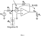
- FIG. 1 illustrates that the internal noise may be modeled as a voltage source V NI in series with the non-inverting input.
- the shunt negative resistance (-R3) produces a current of suitable polarity that flows through resistor R2 to the output, and at least partially cancels the external noise.
- FIG. 2 illustrates that the optimized normalized value of
- 0.5. Therefore, it is desirable to have the negative resistance value be close to but not equal to the optimal value for canceling the internal noise.
- One challenge with setting the negative resistance value close to the value that causes the circuit to go unstable is that variations in the component values due to process voltage or temperature (PVT variations) can result in the negative resistance value drifting to the value at which the circuit goes unstable. Accordingly, would be desirable for the negative resistance circuit to be insensitive to PVT variations.
- circuits described herein produce a small signal negative resistance value and are insensitive to PVT variations.
- cross-coupled transistors may be included that are constant-G m biased in strong inversion or weak inversion.
- FIG. 3 shows an example of a negative resistance circuit 100, according to some embodiments.
- Negative resistance circuit 100 includes a first cross-coupled transistor circuit 110, a second cross-coupled transistor circuit 120, an op-amp 130 and a current source circuit 140.
- the first cross-coupled transistor circuit 110 may be connected to the inverting input of the op-amp of FIG. 1 , also referred to as the summing node Vs.
- the first cross-coupled transistor circuit 110 may be connected to the non-inverting input of op-amp 130 at terminal V X0 .
- the first cross-coupled transistor circuit 110 includes a transistor 111 having its source connected to terminal V X0 and its drain connected to the summing node Vs.
- the first cross-coupled transistor circuit 110 also includes a transistor 112 having its source connected to terminal V X0 and its drain connected to a ground terminal.
- Transistors 111 and 112 have a channel width W and a length L, with a ratio W/L. As illustrated in FIG.
- transistors 111 and 112 are cross-coupled, with the gate of one transistor being connected to the drain of the other transistor. More specifically, transistor 111 has its gate connected to the drain of transistor 112 and transistor 112 has its gate connected to the drain of transistor 111.
- a biasing current is provided to the first cross-coupled transistor circuit 110 by current source 141, which is controlled by the output of op-amp 130.
- the first cross-coupled transistor circuit 110 may be biased using constant-G m biasing.
- the first-cross coupled transistor circuit 110 may be biased in strong inversion or in weak inversion.
- the second cross-coupled transistor circuit 120 may be connected to the inverting input of op-amp 130 at terminal V X1 .
- the second cross-coupled transistor circuit 120 includes a transistor 121 having its source connected to terminal V X1 and its drain connected to the impedance 123.
- the second cross-coupled transistor circuit 120 also includes a transistor 122 having its source connected to terminal V X1 and its drain connected to the impedance 124.
- Transistors 121 and 122 have a channel width to length ratio of M times W/L. As illustrated in FIG. 3 , transistors 121 and 122 are cross-coupled, with the gate of one transistor being connected to the drain of the other transistor.
- transistor 121 has its gate connected to the drain of transistor 122 and transistor 122 has its gate connected to the drain of transistor 121.
- a biasing current is provided to the first cross-coupled transistor circuit 120 by current source 142, which is controlled by the output of op-amp 130.
- the second cross-coupled transistor circuit 120 may be biased using constant-G m biasing.
- the second cross-coupled transistor circuit 120 may be biased in strong inversion or in weak inversion.
- Op-amp 130 maintains V X1 and V X0 at the same voltage.
- the output of op-amp 130 controls the current sources 142 and 141. Accordingly, the negative resistance circuit 100 maintains its (small signal) resistance and is sensitive to PVT variations.
- FIG. 3 shows a single ended version of a negative resistance circuit 100
- a differential version of the negative resistance circuit may be used. For example, instead of connecting the drain of transistor 112 to a ground terminal, a differential signal may be provided across the drains of transistors 111 and 112.
- FIG. 4 shows another example of a negative resistance circuit 200, according to some embodiments.
- An op-amp 230 has its inverting input connected to the source of transistor 221 and its non-inverting input connected to the source of transistor 222.
- Transistors 221 and 222 are each diode connected: their gate is connected to their drain.
- Transistor 222 has a width to length ratio of W/L.
- Transistor 221 has a width to length ratio of M times W/L.
- the op-amp 230 holds the sources of transistors 221 and 222 at the same voltage.
- Transistor 221 is biased by a current source 241, which is controlled by the output of the op-amp 230.
- Transistor 222 is biased by a current source 242, which is controlled by the output of the op-amp 230.
- Transistor 221 is in series with an impedance 225.
- Impedance 225 may be connected between the drain of transistor 225 and ground.
- the drain of transistor 222 may be coupled to ground.
- the transistors 221 and 222 may form a diode-connected replica bias circuit that provides constant constant-G m biasing. Such a replica bias circuit may have the advantage of low power consumption.
- Another advance is that the feedback loop for the constant-G m biasing can be isolated from the main feedback loop.
- a cross-coupled transistor circuit 210 may be connected to the inverting input of the op-amp of FIG. 1 , also referred to as the summing node Vs.
- the cross-coupled transistor circuit 210 includes a transistor 211 having its source connected to current source 243 and its drain connected to the summing node Vs.
- the first cross-coupled transistor circuit 210 also includes a transistor 212 having its source connected to current source 243 and its drain connected to a ground terminal.
- Transistors 211 and 212 each has a channel width to length ratio of K times W/L. As illustrated in FIG. 4 , transistors 211 and 212 are cross-coupled, with the gate of one transistor being connected to the drain of the other transistor.
- transistor 211 has its gate connected to the drain of transistor 212 and transistor 212 has its gate connected to the drain of transistor 211.
- a biasing current is provided to the cross-coupled transistor circuit 210 by current source 243, which is controlled by the output of op-amp 230.
- the cross-coupled transistor circuit 210 may be biased using constant-G m biasing.
- the cross-coupled transistor circuit 210 may be biased in strong inversion or in weak inversion.
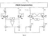
- An optional PMOS complementary circuit 250 may be included. Circuit 250 may enhance the overall Gm of the cross-coupled transistors 211 and 212. NMOS transistors can sink current and PMOS transsitors can push current. Gm will be double for the same current if a PMOS device is also included.
- FIG. 6 illustrates that optionally, an explicit impedance Z may be connected between the sources of transistors 211 and 212 and/or between the sources of transistors 221 and 222. If the sources of transistors 211 and 212 are separated by an impedance Z the current source 243 may be split into two separate current sources 243a and 243b for biasing transistors 211 and 212, respectively.
Landscapes
- Engineering & Computer Science (AREA)
- Power Engineering (AREA)
- Amplifiers (AREA)
Abstract
Description
- The techniques described herein relate generally to negative resistance circuits for reducing noise in operational amplifiers, including in audio applications, for example.
- An operational amplifier or "op-amp" is a widely used amplifier circuit. An operational amplifier has an "inverting input" denoted by the symbol "-" and a non-inverting input denoted by the symbol "+". The inputs of an operational amplifier have a high input impedance. The output of the operational amplifier has a low output impedance. One or more components may be connect between the input(s) and the output. An operational amplifier uses feedback to drive the inverting and non-inverting inputs to the same voltage, also termed a virtual short.
- A circuit includes a first operational amplifier having an inverting input and a non-inverting input; a negative resistance circuit connected to the inverting input of the first operational amplifier, the negative resistance circuit comprising: a second operational amplifier; a current source controlled by the second operational amplifier; and a cross-coupled transistor circuit having at least one transistor biased by a current produced by the current source.
- The at least one transistor may have a source connected to a non-inverting input of the second operational amplifier.
- The cross-coupled transistor circuit may comprise a first transistor; and a second transistor. A gate of the first transistor may be connected to a drain of the second transistor and a gate of the second transistor may be connected to a drain of the first transistor.
- A source of the first transistor and a source of the second transistor may be connected to a non-inverting input of the second operational amplifier.
- The first transistor may have a drain connected to the inverting input of the first operational amplifier and the second transistor may have a drain connected to a ground terminal or a differential input.
- The circuit may further comprise a second cross-coupled transistor circuit having at least one transistor biased by a current produced by a second current source, the second current source being controlled by the second operational amplifier.
- The second cross-coupled transistor circuit may comprise a third transistor; and a fourth transistor, wherein a gate of the third transistor is connected to a drain of the fourth transistor and a gate of the fourth transistor is connected to a drain of the third transistor.
- A source of the third transistor and a source of the fourth transistor may be connected to a non-inverting input of the second operational amplifier.
- The circuit may further comprise a first impedance coupled between the third transistor and ground, and a second impedance coupled between the fourth transistor and ground.
- The circuit may further comprise a first transistor having its source connected to an inverting input of the second operational amplifier; and a second transistor having its source connected to a non-inverting input of the second operational amplifier. The first and second transistors each may have their gate connected to their drain.
- The circuit may further comprise a third current source controlled by the second operational amplifier and biasing the first transistor; and a fourth current source controlled by the second operational amplifier and biasing the second transistor.
- The circuit may further comprise an impedance coupled between the first transistor and a ground terminal.
- The second transistor may have its drain connected to a ground terminal.
- The circuit may have an impedance connected between the sources of the first and second transistors.
- A negative resistance circuit may include an operational amplifier; a current source controlled by the operational amplifier; and a cross-coupled transistor circuit having at least one transistor biased by a current produced by the current source.
- The at least one transistor may have a source connected to a non-inverting input of the operational amplifier.
- The cross-coupled transistor circuit may comprise a first transistor; and a second transistor. A gate of the first transistor may be connected to a drain of the second transistor and a gate of the second transistor may be connected to a drain of the first transistor.
- A source of the first transistor and a source of the second transistor may be connected to a non-inverting input of the operational amplifier.
- The negative resistance circuit may further comprise a first transistor having its source connected to an inverting input of the operational amplifier; and a second transistor having its source connected to a non-inverting input of the operational amplifier. The first and second transistors may each have their gate connected to their drain.
- The negative resistance circuit may further comprise a third current source controlled by the operational amplifier and biasing the first transistor; and a fourth current source controlled by the operational amplifier and biasing the second transistor.
- The foregoing summary is provided by way of illustration and is not intended to be limiting.
- In the drawings, each identical or nearly identical component that is illustrated in various figures is represented by a like reference character. For purposes of clarity, not every component may be labeled in every drawing. The drawings are not necessarily drawn to scale, with emphasis instead being placed on illustrating various aspects of the techniques and devices described herein.
-
FIG. 1 illustrates that the internal noise of an operational amplifier may be modeled as a voltage source in series with the non-inverting input. -
FIG. 2 illustrates the feedback factor beta over a range of values of normalized absolute value of R3. -
FIG. 3 shows an example of a negative resistance circuit, according to some embodiments. -
FIG. 4 shows an example of a negative resistance circuit using diode-connected transistors, according to some embodiments. -
FIG. 5 shows an example of a complementary PMOS circuit, according to some embodiments. -
FIG. 6 shows an example of a negative resistance circuit using diode-connected transistors and explicit impedances Z, according to some embodiments. - Op-amps have internal noise that may appear in the output signal. Although an op-amp may be designed to have reduced internal noise, doing so may increase power dissipation. Accordingly, it is desirable to use a different technique to reduce the internal noise appearing in the output signal.
- It has been appreciated that a shunt negative resistance value between the non-inverting input and ground can at least partially cancel the internal noise of the op-amp.
FIG. 1 illustrates that the internal noise may be modeled as a voltage source VNI in series with the non-inverting input. The shunt negative resistance (-R3) produces a current of suitable polarity that flows through resistor R2 to the output, and at least partially cancels the external noise. - One challenge with such an approach is the optimum value of negative resistance to cancel the internal noise of the operational amplifier can cause the circuit to become unstable.
FIG. 2 illustrates that the optimized normalized value of |R3| is 0.5, with the feedback factor (β) going to infinity or negative infinity on either side of 0.5, which indicates the circuit is unstable at |R3| = 0.5. Therefore, it is desirable to have the negative resistance value be close to but not equal to the optimal value for canceling the internal noise. One challenge with setting the negative resistance value close to the value that causes the circuit to go unstable is that variations in the component values due to process voltage or temperature (PVT variations) can result in the negative resistance value drifting to the value at which the circuit goes unstable. Accordingly, would be desirable for the negative resistance circuit to be insensitive to PVT variations. - The circuits described herein produce a small signal negative resistance value and are insensitive to PVT variations. In some embodiments, cross-coupled transistors may be included that are constant-Gm biased in strong inversion or weak inversion.
-
FIG. 3 shows an example of anegative resistance circuit 100, according to some embodiments.Negative resistance circuit 100 includes a firstcross-coupled transistor circuit 110, a secondcross-coupled transistor circuit 120, an op-amp 130 and acurrent source circuit 140. - The first
cross-coupled transistor circuit 110 may be connected to the inverting input of the op-amp ofFIG. 1 , also referred to as the summing node Vs. The firstcross-coupled transistor circuit 110 may be connected to the non-inverting input of op-amp 130 at terminal VX0. The firstcross-coupled transistor circuit 110 includes atransistor 111 having its source connected to terminal VX0 and its drain connected to the summing node Vs. The firstcross-coupled transistor circuit 110 also includes atransistor 112 having its source connected to terminal VX0 and its drain connected to a ground terminal.Transistors FIG. 3 ,transistors transistor 111 has its gate connected to the drain oftransistor 112 andtransistor 112 has its gate connected to the drain oftransistor 111. A biasing current is provided to the firstcross-coupled transistor circuit 110 bycurrent source 141, which is controlled by the output of op-amp 130. In some embodiments, the firstcross-coupled transistor circuit 110 may be biased using constant-Gm biasing. The first-cross coupledtransistor circuit 110 may be biased in strong inversion or in weak inversion. - The second
cross-coupled transistor circuit 120 may be connected to the inverting input of op-amp 130 at terminal VX1. The secondcross-coupled transistor circuit 120 includes atransistor 121 having its source connected to terminal VX1 and its drain connected to theimpedance 123. The secondcross-coupled transistor circuit 120 also includes atransistor 122 having its source connected to terminal VX1 and its drain connected to theimpedance 124.Transistors FIG. 3 ,transistors transistor 121 has its gate connected to the drain oftransistor 122 andtransistor 122 has its gate connected to the drain oftransistor 121. A biasing current is provided to the firstcross-coupled transistor circuit 120 bycurrent source 142, which is controlled by the output of op-amp 130. In some embodiments, the secondcross-coupled transistor circuit 120 may be biased using constant-Gm biasing. The secondcross-coupled transistor circuit 120 may be biased in strong inversion or in weak inversion. - Op-
amp 130 maintains VX1 and VX0 at the same voltage. The output of op-amp 130 controls thecurrent sources negative resistance circuit 100 maintains its (small signal) resistance and is sensitive to PVT variations. - Although
FIG. 3 shows a single ended version of anegative resistance circuit 100, a differential version of the negative resistance circuit may be used. For example, instead of connecting the drain oftransistor 112 to a ground terminal, a differential signal may be provided across the drains oftransistors -
FIG. 4 shows another example of anegative resistance circuit 200, according to some embodiments. An op-amp 230 has its inverting input connected to the source oftransistor 221 and its non-inverting input connected to the source oftransistor 222.Transistors Transistor 222 has a width to length ratio of W/L. Transistor 221 has a width to length ratio of M times W/L. The op-amp 230 holds the sources oftransistors Transistor 221 is biased by acurrent source 241, which is controlled by the output of the op-amp 230.Transistor 222 is biased by acurrent source 242, which is controlled by the output of the op-amp 230.Transistor 221 is in series with animpedance 225.Impedance 225 may be connected between the drain oftransistor 225 and ground. The drain oftransistor 222 may be coupled to ground. Thetransistors - A
cross-coupled transistor circuit 210 may be connected to the inverting input of the op-amp ofFIG. 1 , also referred to as the summing node Vs. Thecross-coupled transistor circuit 210 includes atransistor 211 having its source connected tocurrent source 243 and its drain connected to the summing node Vs. The firstcross-coupled transistor circuit 210 also includes atransistor 212 having its source connected tocurrent source 243 and its drain connected to a ground terminal.Transistors FIG. 4 ,transistors transistor 211 has its gate connected to the drain oftransistor 212 andtransistor 212 has its gate connected to the drain oftransistor 211. A biasing current is provided to thecross-coupled transistor circuit 210 bycurrent source 243, which is controlled by the output of op-amp 230. In some embodiments, thecross-coupled transistor circuit 210 may be biased using constant-Gm biasing. Thecross-coupled transistor circuit 210 may be biased in strong inversion or in weak inversion. - An optional PMOS
complementary circuit 250 may be included.Circuit 250 may enhance the overall Gm of thecross-coupled transistors FIG. 5 shows an example of a PMOScomplementary circuit 250. If INN is connected to ground, INP sees an input impedance of -1/Gm assuming Gmp=Gmn=Gm. Points A, B, C and D inFIG. 5 may connected to the corresponding points inFIGS. 4 and6 . -
FIG. 6 illustrates that optionally, an explicit impedance Z may be connected between the sources oftransistors transistors transistors current source 243 may be split into two separatecurrent sources transistors - Various aspects of the apparatus and techniques described herein may be used alone, in combination, or in a variety of arrangements not specifically discussed in the embodiments described in the foregoing description and is therefore not limited in its application to the details and arrangement of components set forth in the foregoing description or illustrated in the drawings. For example, aspects described in one embodiment may be combined in any manner with aspects described in other embodiments.
- Use of ordinal terms such as "first," "second," "third," etc., in the claims to modify a claim element does not by itself connote any priority, precedence, or order of one claim element over another or the temporal order in which acts of a method are performed, but are used merely as labels to distinguish one claim element having a certain name from another element having a same name (but for use of the ordinal term) to distinguish the claim elements.
- Also, the phraseology and terminology used herein is for the purpose of description and should not be regarded as limiting. The use of "including," "comprising," or "having," "containing," "involving," and variations thereof herein, is meant to encompass the items listed thereafter and equivalents thereof as well as additional items.
Claims (14)
- A circuit, comprising:a first operational amplifier having an inverting input and a non-inverting input;a negative resistance circuit connected to the inverting input of the first operational amplifier, the negative resistance circuit comprising:a second operational amplifier;a current source controlled by the second operational amplifier; anda cross-coupled transistor circuit having at least one transistor biased by a current produced by the current source.
- The circuit of claim 1, wherein the at least one transistor has a source connected to a non-inverting input of the second operational amplifier.
- The circuit of any preceding claim, wherein the cross-coupled transistor circuit comprises:a first transistor; anda second transistor,wherein a gate of the first transistor is connected to a drain of the second transistor and a gate of the second transistor is connected to a drain of the first transistor.
- The circuit of claim 3, wherein a source of the first transistor and a source of the second transistor are connected to a non-inverting input of the second operational amplifier.
- The circuit of claim 4, wherein the first transistor has a drain connected to the inverting input of the first operational amplifier and the second transistor has a drain connected to a ground terminal or a differential input.
- The circuit of any preceding claim, further comprising a second cross-coupled transistor circuit having at least one transistor biased by a current produced by a second current source, the second current source being controlled by the second operational amplifier.
- The circuit of claim 6, wherein the second cross-coupled transistor circuit comprises:a third transistor; anda fourth transistor,wherein a gate of the third transistor is connected to a drain of the fourth transistor and a gate of the fourth transistor is connected to a drain of the third transistor.
- The circuit of claim 7, wherein a source of the third transistor and a source of the fourth transistor are connected to a non-inverting input of the second operational amplifier.
- The circuit of claim 8, further comprising a first impedance coupled between the third transistor and ground, and a second impedance coupled between the fourth transistor and ground.
- The circuit of claim 1, further comprising:a first transistor having its source connected to an inverting input of the second operational amplifier; anda second transistor having its source connected to a non-inverting input of the second operational amplifier,wherein the first and second transistors each have their gate connected to their drain.
- The circuit of claim 10, further comprising:a third current source controlled by the second operational amplifier and biasing the first transistor; anda fourth current source controlled by the second operational amplifier and biasing the second transistor.
- The circuit of claim 11, further comprising an impedance coupled between the first transistor and a ground terminal.
- The circuit of claim 12, wherein the second transistor has its drain connected to a ground terminal.
- The circuit of claim 13, having an impedance connected between the sources of the first and second transistors.
Applications Claiming Priority (2)
| Application Number | Priority Date | Filing Date | Title |
|---|---|---|---|
| US201962830639P | 2019-04-08 | 2019-04-08 | |
| US16/840,537 US11228283B2 (en) | 2019-04-08 | 2020-04-06 | Negative impedance circuit for reducing amplifier noise |
Publications (2)
| Publication Number | Publication Date |
|---|---|
| EP3723283A1 true EP3723283A1 (en) | 2020-10-14 |
| EP3723283B1 EP3723283B1 (en) | 2022-12-21 |
Family
ID=70227911
Family Applications (1)
| Application Number | Title | Priority Date | Filing Date |
|---|---|---|---|
| EP20168573.2A Active EP3723283B1 (en) | 2019-04-08 | 2020-04-07 | Negative impedance circuit for reducing amplifier noise |
Country Status (2)
| Country | Link |
|---|---|
| US (1) | US11228283B2 (en) |
| EP (1) | EP3723283B1 (en) |
Families Citing this family (1)
| Publication number | Priority date | Publication date | Assignee | Title |
|---|---|---|---|---|
| CN116232234B (en) * | 2022-09-06 | 2025-08-15 | 苏州大学 | High-gain operational amplifier circuit based on negative resistance technology |
Citations (2)
| Publication number | Priority date | Publication date | Assignee | Title |
|---|---|---|---|---|
| US8963641B1 (en) * | 2013-03-15 | 2015-02-24 | Maxim Integrated Products, Inc. | Source-series terminated differential line driver circuit |
| US9621136B1 (en) * | 2015-11-12 | 2017-04-11 | Nxp Usa, Inc. | Data sampler circuit with equalization function and method for sampling data |
Family Cites Families (14)
| Publication number | Priority date | Publication date | Assignee | Title |
|---|---|---|---|---|
| US4001735A (en) | 1975-11-20 | 1977-01-04 | Northern Electric Company Limited | Single amplifier immittance network |
| FR2739936B1 (en) | 1995-10-11 | 1997-11-14 | Snecma | DIFFERENTIAL CHARGE AMPLIFIER FOR PIEZOELECTRIC SENSOR |
| WO2003017487A1 (en) | 2001-08-16 | 2003-02-27 | Koninklijke Philips Electronics N.V. | Ring oscillator stage |
| TW544995B (en) | 2002-08-09 | 2003-08-01 | Advanic Technologies Inc | Flash A/D converter with new autozeroing and interpolation possessing negative impedance compensation |
| KR100558571B1 (en) * | 2004-03-03 | 2006-03-13 | 삼성전자주식회사 | Current Sense Amplifier Circuit of Semiconductor Memory Device |
| US7126431B2 (en) * | 2004-11-30 | 2006-10-24 | Stmicroelectronics, Inc. | Differential delay cell having controllable amplitude output |
| TWI305976B (en) | 2005-12-30 | 2009-02-01 | Ind Tech Res Inst | Transimpedance amplifier using negative impedance compensation |
| KR100866705B1 (en) | 2007-07-04 | 2008-11-03 | 주식회사 하이닉스반도체 | Semiconductor memory device using ferroelectric element |
| US8421433B2 (en) * | 2010-03-31 | 2013-04-16 | Maxim Integrated Products, Inc. | Low noise bandgap references |
| US8548410B2 (en) * | 2011-11-30 | 2013-10-01 | St-Ericsson Sa | RF front-end for intra-band carrier aggregation |
| US9263997B2 (en) | 2013-03-14 | 2016-02-16 | Quantance, Inc. | Self setting power supply using negative output impedance |
| WO2018076173A1 (en) | 2016-10-25 | 2018-05-03 | 深圳市汇顶科技股份有限公司 | Amplitude-limit oscillation circuit |
| US10003374B1 (en) * | 2017-11-29 | 2018-06-19 | National Cheng Kung University | Wireless radio frequency transceiver system for internet of things |
| US11048990B2 (en) * | 2019-02-12 | 2021-06-29 | The Board Of Trustees Of The Leland Stanford Junior University | Resonance-based inductive communication via frequency sweeping |
-
2020
- 2020-04-06 US US16/840,537 patent/US11228283B2/en active Active
- 2020-04-07 EP EP20168573.2A patent/EP3723283B1/en active Active
Patent Citations (2)
| Publication number | Priority date | Publication date | Assignee | Title |
|---|---|---|---|---|
| US8963641B1 (en) * | 2013-03-15 | 2015-02-24 | Maxim Integrated Products, Inc. | Source-series terminated differential line driver circuit |
| US9621136B1 (en) * | 2015-11-12 | 2017-04-11 | Nxp Usa, Inc. | Data sampler circuit with equalization function and method for sampling data |
Also Published As
| Publication number | Publication date |
|---|---|
| US20200321919A1 (en) | 2020-10-08 |
| EP3723283B1 (en) | 2022-12-21 |
| US11228283B2 (en) | 2022-01-18 |
Similar Documents
| Publication | Publication Date | Title |
|---|---|---|
| US6407623B1 (en) | Bias circuit for maintaining a constant value of transconductance divided by load capacitance | |
| US4554515A (en) | CMOS Operational amplifier | |
| US4333058A (en) | Operational amplifier employing complementary field-effect transistors | |
| US6469579B2 (en) | Boosted high gain, very wide common mode range, self-biased operational amplifier | |
| KR950004709A (en) | MOS Differential Voltage-to-Current Conversion Circuit | |
| CA2233527C (en) | Pulse amplifier with low-duty cycle errors | |
| US20020171486A1 (en) | High gain, high bandwidth, fully differential amplifier | |
| US5043652A (en) | Differential voltage to differential current conversion circuit having linear output | |
| US4533877A (en) | Telecommunication operational amplifier | |
| US11228283B2 (en) | Negative impedance circuit for reducing amplifier noise | |
| JPH0235485B2 (en) | ||
| EP0632582B1 (en) | Operational amplifier and method | |
| US20040239426A1 (en) | Operational amplifier generating desired feedback reference voltage allowing improved output characteristic | |
| IE59331B1 (en) | Field-effect transistor amplifier circuits | |
| US6798292B1 (en) | Highly linear low voltage rail-to-rail input/output operational amplifier | |
| US6815997B2 (en) | Field effect transistor square multiplier | |
| US7259626B2 (en) | Apparatus and method for biasing cascode devices in a differential pair using the input, output, or other nodes in the circuit | |
| US6496066B2 (en) | Fully differential operational amplifier of the folded cascode type | |
| TWI758155B (en) | Circuit for reducing amplifier noise and negative impedance | |
| US6831501B1 (en) | Common-mode controlled differential gain boosting | |
| US20100295619A1 (en) | Low Noise Amplifier | |
| US7005921B2 (en) | Common-mode feedback circuit | |
| US20010035776A1 (en) | Fixed transconductance bias apparatus | |
| Eldeeb et al. | A 0.4 V 90nm CMOS subthreshold current conveyor | |
| US6069532A (en) | Technique for designing a bias circuit for an amplifier in an integrated circuit device |
Legal Events
| Date | Code | Title | Description |
|---|---|---|---|
| PUAI | Public reference made under article 153(3) epc to a published international application that has entered the european phase |
Free format text: ORIGINAL CODE: 0009012 |
|
| STAA | Information on the status of an ep patent application or granted ep patent |
Free format text: STATUS: THE APPLICATION HAS BEEN PUBLISHED |
|
| AK | Designated contracting states |
Kind code of ref document: A1 Designated state(s): AL AT BE BG CH CY CZ DE DK EE ES FI FR GB GR HR HU IE IS IT LI LT LU LV MC MK MT NL NO PL PT RO RS SE SI SK SM TR |
|
| AX | Request for extension of the european patent |
Extension state: BA ME |
|
| STAA | Information on the status of an ep patent application or granted ep patent |
Free format text: STATUS: REQUEST FOR EXAMINATION WAS MADE |
|
| 17P | Request for examination filed |
Effective date: 20210413 |
|
| RBV | Designated contracting states (corrected) |
Designated state(s): AL AT BE BG CH CY CZ DE DK EE ES FI FR GB GR HR HU IE IS IT LI LT LU LV MC MK MT NL NO PL PT RO RS SE SI SK SM TR |
|
| STAA | Information on the status of an ep patent application or granted ep patent |
Free format text: STATUS: EXAMINATION IS IN PROGRESS |
|
| 17Q | First examination report despatched |
Effective date: 20220517 |
|
| GRAP | Despatch of communication of intention to grant a patent |
Free format text: ORIGINAL CODE: EPIDOSNIGR1 |
|
| STAA | Information on the status of an ep patent application or granted ep patent |
Free format text: STATUS: GRANT OF PATENT IS INTENDED |
|
| INTG | Intention to grant announced |
Effective date: 20220916 |
|
| GRAS | Grant fee paid |
Free format text: ORIGINAL CODE: EPIDOSNIGR3 |
|
| GRAA | (expected) grant |
Free format text: ORIGINAL CODE: 0009210 |
|
| STAA | Information on the status of an ep patent application or granted ep patent |
Free format text: STATUS: THE PATENT HAS BEEN GRANTED |
|
| AK | Designated contracting states |
Kind code of ref document: B1 Designated state(s): AL AT BE BG CH CY CZ DE DK EE ES FI FR GB GR HR HU IE IS IT LI LT LU LV MC MK MT NL NO PL PT RO RS SE SI SK SM TR |
|
| RAP3 | Party data changed (applicant data changed or rights of an application transferred) |
Owner name: MEDIATEK SINGAPORE PTE. LTD. |
|
| REG | Reference to a national code |
Ref country code: GB Ref legal event code: FG4D |
|
| REG | Reference to a national code |
Ref country code: CH Ref legal event code: EP |
|
| REG | Reference to a national code |
Ref country code: DE Ref legal event code: R096 Ref document number: 602020007004 Country of ref document: DE |
|
| REG | Reference to a national code |
Ref country code: AT Ref legal event code: REF Ref document number: 1539647 Country of ref document: AT Kind code of ref document: T Effective date: 20230115 |
|
| REG | Reference to a national code |
Ref country code: IE Ref legal event code: FG4D |
|
| REG | Reference to a national code |
Ref country code: LT Ref legal event code: MG9D |
|
| REG | Reference to a national code |
Ref country code: NL Ref legal event code: MP Effective date: 20221221 |
|
| PG25 | Lapsed in a contracting state [announced via postgrant information from national office to epo] |
Ref country code: SE Free format text: LAPSE BECAUSE OF FAILURE TO SUBMIT A TRANSLATION OF THE DESCRIPTION OR TO PAY THE FEE WITHIN THE PRESCRIBED TIME-LIMIT Effective date: 20221221 Ref country code: NO Free format text: LAPSE BECAUSE OF FAILURE TO SUBMIT A TRANSLATION OF THE DESCRIPTION OR TO PAY THE FEE WITHIN THE PRESCRIBED TIME-LIMIT Effective date: 20230321 Ref country code: LT Free format text: LAPSE BECAUSE OF FAILURE TO SUBMIT A TRANSLATION OF THE DESCRIPTION OR TO PAY THE FEE WITHIN THE PRESCRIBED TIME-LIMIT Effective date: 20221221 Ref country code: FI Free format text: LAPSE BECAUSE OF FAILURE TO SUBMIT A TRANSLATION OF THE DESCRIPTION OR TO PAY THE FEE WITHIN THE PRESCRIBED TIME-LIMIT Effective date: 20221221 |
|
| REG | Reference to a national code |
Ref country code: AT Ref legal event code: MK05 Ref document number: 1539647 Country of ref document: AT Kind code of ref document: T Effective date: 20221221 |
|
| PG25 | Lapsed in a contracting state [announced via postgrant information from national office to epo] |
Ref country code: RS Free format text: LAPSE BECAUSE OF FAILURE TO SUBMIT A TRANSLATION OF THE DESCRIPTION OR TO PAY THE FEE WITHIN THE PRESCRIBED TIME-LIMIT Effective date: 20221221 Ref country code: LV Free format text: LAPSE BECAUSE OF FAILURE TO SUBMIT A TRANSLATION OF THE DESCRIPTION OR TO PAY THE FEE WITHIN THE PRESCRIBED TIME-LIMIT Effective date: 20221221 Ref country code: HR Free format text: LAPSE BECAUSE OF FAILURE TO SUBMIT A TRANSLATION OF THE DESCRIPTION OR TO PAY THE FEE WITHIN THE PRESCRIBED TIME-LIMIT Effective date: 20221221 Ref country code: GR Free format text: LAPSE BECAUSE OF FAILURE TO SUBMIT A TRANSLATION OF THE DESCRIPTION OR TO PAY THE FEE WITHIN THE PRESCRIBED TIME-LIMIT Effective date: 20230322 |
|
| PG25 | Lapsed in a contracting state [announced via postgrant information from national office to epo] |
Ref country code: NL Free format text: LAPSE BECAUSE OF FAILURE TO SUBMIT A TRANSLATION OF THE DESCRIPTION OR TO PAY THE FEE WITHIN THE PRESCRIBED TIME-LIMIT Effective date: 20221221 |
|
| PG25 | Lapsed in a contracting state [announced via postgrant information from national office to epo] |
Ref country code: SM Free format text: LAPSE BECAUSE OF FAILURE TO SUBMIT A TRANSLATION OF THE DESCRIPTION OR TO PAY THE FEE WITHIN THE PRESCRIBED TIME-LIMIT Effective date: 20221221 Ref country code: RO Free format text: LAPSE BECAUSE OF FAILURE TO SUBMIT A TRANSLATION OF THE DESCRIPTION OR TO PAY THE FEE WITHIN THE PRESCRIBED TIME-LIMIT Effective date: 20221221 Ref country code: PT Free format text: LAPSE BECAUSE OF FAILURE TO SUBMIT A TRANSLATION OF THE DESCRIPTION OR TO PAY THE FEE WITHIN THE PRESCRIBED TIME-LIMIT Effective date: 20230421 Ref country code: ES Free format text: LAPSE BECAUSE OF FAILURE TO SUBMIT A TRANSLATION OF THE DESCRIPTION OR TO PAY THE FEE WITHIN THE PRESCRIBED TIME-LIMIT Effective date: 20221221 Ref country code: EE Free format text: LAPSE BECAUSE OF FAILURE TO SUBMIT A TRANSLATION OF THE DESCRIPTION OR TO PAY THE FEE WITHIN THE PRESCRIBED TIME-LIMIT Effective date: 20221221 Ref country code: CZ Free format text: LAPSE BECAUSE OF FAILURE TO SUBMIT A TRANSLATION OF THE DESCRIPTION OR TO PAY THE FEE WITHIN THE PRESCRIBED TIME-LIMIT Effective date: 20221221 Ref country code: AT Free format text: LAPSE BECAUSE OF FAILURE TO SUBMIT A TRANSLATION OF THE DESCRIPTION OR TO PAY THE FEE WITHIN THE PRESCRIBED TIME-LIMIT Effective date: 20221221 |
|
| P01 | Opt-out of the competence of the unified patent court (upc) registered |
Effective date: 20230627 |
|
| PG25 | Lapsed in a contracting state [announced via postgrant information from national office to epo] |
Ref country code: SK Free format text: LAPSE BECAUSE OF FAILURE TO SUBMIT A TRANSLATION OF THE DESCRIPTION OR TO PAY THE FEE WITHIN THE PRESCRIBED TIME-LIMIT Effective date: 20221221 Ref country code: PL Free format text: LAPSE BECAUSE OF FAILURE TO SUBMIT A TRANSLATION OF THE DESCRIPTION OR TO PAY THE FEE WITHIN THE PRESCRIBED TIME-LIMIT Effective date: 20221221 Ref country code: IS Free format text: LAPSE BECAUSE OF FAILURE TO SUBMIT A TRANSLATION OF THE DESCRIPTION OR TO PAY THE FEE WITHIN THE PRESCRIBED TIME-LIMIT Effective date: 20230421 Ref country code: AL Free format text: LAPSE BECAUSE OF FAILURE TO SUBMIT A TRANSLATION OF THE DESCRIPTION OR TO PAY THE FEE WITHIN THE PRESCRIBED TIME-LIMIT Effective date: 20221221 |
|
| REG | Reference to a national code |
Ref country code: DE Ref legal event code: R097 Ref document number: 602020007004 Country of ref document: DE |
|
| PLBE | No opposition filed within time limit |
Free format text: ORIGINAL CODE: 0009261 |
|
| STAA | Information on the status of an ep patent application or granted ep patent |
Free format text: STATUS: NO OPPOSITION FILED WITHIN TIME LIMIT |
|
| PG25 | Lapsed in a contracting state [announced via postgrant information from national office to epo] |
Ref country code: DK Free format text: LAPSE BECAUSE OF FAILURE TO SUBMIT A TRANSLATION OF THE DESCRIPTION OR TO PAY THE FEE WITHIN THE PRESCRIBED TIME-LIMIT Effective date: 20221221 |
|
| 26N | No opposition filed |
Effective date: 20230922 |
|
| REG | Reference to a national code |
Ref country code: CH Ref legal event code: PL |
|
| PG25 | Lapsed in a contracting state [announced via postgrant information from national office to epo] |
Ref country code: LU Free format text: LAPSE BECAUSE OF NON-PAYMENT OF DUE FEES Effective date: 20230407 |
|
| REG | Reference to a national code |
Ref country code: BE Ref legal event code: MM Effective date: 20230430 |
|
| PG25 | Lapsed in a contracting state [announced via postgrant information from national office to epo] |
Ref country code: MC Free format text: LAPSE BECAUSE OF FAILURE TO SUBMIT A TRANSLATION OF THE DESCRIPTION OR TO PAY THE FEE WITHIN THE PRESCRIBED TIME-LIMIT Effective date: 20221221 |
|
| PG25 | Lapsed in a contracting state [announced via postgrant information from national office to epo] |
Ref country code: SI Free format text: LAPSE BECAUSE OF FAILURE TO SUBMIT A TRANSLATION OF THE DESCRIPTION OR TO PAY THE FEE WITHIN THE PRESCRIBED TIME-LIMIT Effective date: 20221221 Ref country code: MC Free format text: LAPSE BECAUSE OF FAILURE TO SUBMIT A TRANSLATION OF THE DESCRIPTION OR TO PAY THE FEE WITHIN THE PRESCRIBED TIME-LIMIT Effective date: 20221221 Ref country code: LI Free format text: LAPSE BECAUSE OF NON-PAYMENT OF DUE FEES Effective date: 20230430 Ref country code: CH Free format text: LAPSE BECAUSE OF NON-PAYMENT OF DUE FEES Effective date: 20230430 |
|
| REG | Reference to a national code |
Ref country code: IE Ref legal event code: MM4A |
|
| PG25 | Lapsed in a contracting state [announced via postgrant information from national office to epo] |
Ref country code: BE Free format text: LAPSE BECAUSE OF NON-PAYMENT OF DUE FEES Effective date: 20230430 |
|
| PG25 | Lapsed in a contracting state [announced via postgrant information from national office to epo] |
Ref country code: IE Free format text: LAPSE BECAUSE OF NON-PAYMENT OF DUE FEES Effective date: 20230407 |
|
| PG25 | Lapsed in a contracting state [announced via postgrant information from national office to epo] |
Ref country code: IE Free format text: LAPSE BECAUSE OF NON-PAYMENT OF DUE FEES Effective date: 20230407 |
|
| PG25 | Lapsed in a contracting state [announced via postgrant information from national office to epo] |
Ref country code: IT Free format text: LAPSE BECAUSE OF FAILURE TO SUBMIT A TRANSLATION OF THE DESCRIPTION OR TO PAY THE FEE WITHIN THE PRESCRIBED TIME-LIMIT Effective date: 20221221 |
|
| PG25 | Lapsed in a contracting state [announced via postgrant information from national office to epo] |
Ref country code: BG Free format text: LAPSE BECAUSE OF FAILURE TO SUBMIT A TRANSLATION OF THE DESCRIPTION OR TO PAY THE FEE WITHIN THE PRESCRIBED TIME-LIMIT Effective date: 20221221 |
|
| PG25 | Lapsed in a contracting state [announced via postgrant information from national office to epo] |
Ref country code: BG Free format text: LAPSE BECAUSE OF FAILURE TO SUBMIT A TRANSLATION OF THE DESCRIPTION OR TO PAY THE FEE WITHIN THE PRESCRIBED TIME-LIMIT Effective date: 20221221 |
|
| PGFP | Annual fee paid to national office [announced via postgrant information from national office to epo] |
Ref country code: DE Payment date: 20250311 Year of fee payment: 6 |
|
| PG25 | Lapsed in a contracting state [announced via postgrant information from national office to epo] |
Ref country code: CY Free format text: LAPSE BECAUSE OF FAILURE TO SUBMIT A TRANSLATION OF THE DESCRIPTION OR TO PAY THE FEE WITHIN THE PRESCRIBED TIME-LIMIT; INVALID AB INITIO Effective date: 20200407 |
|
| PG25 | Lapsed in a contracting state [announced via postgrant information from national office to epo] |
Ref country code: HU Free format text: LAPSE BECAUSE OF FAILURE TO SUBMIT A TRANSLATION OF THE DESCRIPTION OR TO PAY THE FEE WITHIN THE PRESCRIBED TIME-LIMIT; INVALID AB INITIO Effective date: 20200407 |
|
| PG25 | Lapsed in a contracting state [announced via postgrant information from national office to epo] |
Ref country code: TR Free format text: LAPSE BECAUSE OF FAILURE TO SUBMIT A TRANSLATION OF THE DESCRIPTION OR TO PAY THE FEE WITHIN THE PRESCRIBED TIME-LIMIT Effective date: 20221221 |
|
| PGFP | Annual fee paid to national office [announced via postgrant information from national office to epo] |
Ref country code: GB Payment date: 20260216 Year of fee payment: 7 |
|
| PGFP | Annual fee paid to national office [announced via postgrant information from national office to epo] |
Ref country code: FR Payment date: 20260209 Year of fee payment: 7 |